towards asynchronous ad conversion
TRANSCRIPT

Towards Asynchronous A-D Conversion �D.J.Kinniment, B.Gao A.V.Yakovlev, F.XiaDept. of Electrical and Electronic Eng. Dept. of Computing ScienceUniversity of Newcastle upon TyneNewcastle upon Tyne NE1 7RU, UKAbstractAnalogue to digital (A-D) converters with a �xed conversion time are subject to errors due tometastability. These errors will occur in all converter designs with a bounded time for decisions,and are potentially severe. We estimate the frequency of these errors in a successive approximationconverter, and compare the results with asynchronous designs using both a fully speed-independent,and a bundled data approach. It is shown that an asynchronous converter is more reliable thanits synchronous counterpart, and that the bundled data design is also faster, on average, than thesynchronous design. We also demonstrate tradeo�s involved in asynchronous converter designs,such as speed, robustness to delay variations, circuit size and design scalability.Keywords: analogue to digital conversion, arbitration, asynchronous circuits, metastability,signal transition graphs, synchronisers.1 IntroductionN-bit analogue to digital (A-D) converters are usually speci�ed to have a �xed conversion time, butconversion cannot be done in bounded time with complete reliability, since it requires the resolution ofa continuous variable into 2n discrete states. Because the analogue input can be in�nitely close to therequired boundary between two states, metastability can always be caused in the state determininghardware, and such behaviour has been reported [1]. The problem is closely related to that of arbitra-tion between two or more asynchronous requests since in that case the time between requests [2, 3] isin�nitely variable, and must be resolved into one of two or more discrete outcomes. At its root, theproblem arises from the fact that there are in�nitely more real numbers than there are integers [4],and that the physical mechanism used to determine the state has a limited gain-bandwidth product.We can therefore have a decision with a �nite probability of error in a �xed time, or a decision with aguaranteed accuracy which may require in�nite time, and proofs of this fact have been published [5, 6].Analysis of the behaviour of metastability [3, 7] has shown that the probability of the outputremaining in a metastable region decreases exponentially with time, and that therefore the probabilityof error resulting from a bounded decision time also decreases exponentially. If these errors werecon�ned to the least signi�cant bit, the consequent problems would not be serious, but it can beshown that metastability in the most signi�cant bit can result in an error of a quarter of full scale or�This work is supported by EPSRC, GR/K70175 (Project HADES)1

more, and it is important that such problems are understood. An asynchronous comparator based onpreviously reported arbiters [3, 7], can be built which allows su�cient time for a decision to be made,and asynchronous converters based on this component have an exponentially decreasing probabilityof conversion times longer than a minimum time. Such a converter can be both more reliable, and,on average, faster than the conventional, bounded time converter. The latter is clocked on a bitwisebasis and hence is prone to errors due to metastability in high-signi�cance bits. The asynchronousone, even if working within bounds on the overall conversion time is likely to be a�ected only in itslow-signi�cance bits.In this paper we use the SPICE simulator to model a simple successive approximation A-D con-verter, then show that quite signi�cant errors can arise. The probability of error as a function of clockperiod is then given and compared with theory. Two types of self-timed converters are then modelledand their performance measured, showing that data errors due to metastability can be eliminated, andthat the self-timed systems can be both more reliable and have a better performance. The �rst type ofdesign is based on a bundled data (BD) approach. Although it employs an asynchronous metastabilityresolver, it uses fairly tight assumptions about delays in the parts of the logic circuit which are meantto work in parallel. The second type is based on speed-independent (SI) logic, using explicit comple-tion detection logic and individual gate acknowledgement. It is designed from a formal behaviouralspeci�cation, a Signal Transition Graph, using appropriate synthesis techniques and software tool pet-rify [8]. The SI design (three options have been studied, di�erent in their logic complexity and designscalability) loses to the BD one in speed but gains in robustness of the implementation if the physicaldelay parameters of logic gates are variable.2 Synchronous A-D Converter2.1 Basic algorithm and converter modelWe have designed a simple CMOS 4 bit successive approximation A-D converter based on the diagramof Figure 1. The comparator is designed to respond to a voltage di�erence of half the least signi�cantbit within 4 nS, and the remaining loop delays are less than 4 nS. This has been simulated usingthe MIETEC 2� CMOS SPICE model, and the analogue input carefully adjusted until metastabilityoccurred in the most signi�cant bit of the output.The internal state and output registers are based on a master-slave in which a positive edge onthe clock causes the master to latch, and the slave to become transparent. If there is a con ict,or indeterminate levels at the master set and reset inputs when the clock goes high, this may causemetastability, which could result in a change at the slave output at a timemuch later than the followingpositive clock edge. The 4-bit converter follows the steps of the algorithm shown in Table 1; it goesthrough 5 states in order to complete and output a digital sample.2.2 Synchronous converter resultsThe converter is clocked every 10 nS as shown in the HSPICE waveforms of Figure 2. The converterenters state 1 at 6 nS following the positive going clock edge at 5.5 nS. The output, CB3 { CB0 thengoes to 1000 and the D-A converter responds at 7.5 nS producing an output close to the analogue2

��������������������������������������������������������������������������������������������������������������������������������������������������������������������������������������������������������������������������������������������������������������������������������������������������������������������������������������������������������������������������������������������������������������������������������������������������������������������������������������������������������������������
Figure 1: Synchronous Analogue to Digital ConverterReady State MSB CB2 CB1 LSB(CB3) (CB0)1 0 X X X X0 1 1 0 0 00 2 Comp 1 0 00 3 X Comp 1 00 4 X X Comp 11 0 X X X CompTable 1: Control of Converter (`X' stands for any value, `Comp' denotes the value produced by com-parator)input. At about 13 nS the comparator output goes high, and the master CB3 output (waveformXX3.Q) moves to low at 14 nS, because the clock is low. At 15.5 nS the clock goes high again, andCB3 is trapped in metastability. If the output of CB3 were to go to either a high or a low state before20 nS, the subsequent conversion would end at 1000 or 0111, but the half level output from the master,allows CB3 slave output to stay high, and when the master �nally goes low at 21 nS CB3 outputchanges state too late to prevent CB2, which has been responding to the high output of CB3, beingreset low. The result is a value of 0011. If the metastability were to last for the full conversion timebefore going to zero, which is less likely but still possible, the result could be 0000. These outputsrepresent potentially disastrous errors of a quarter and a half full scale respectively.2.3 Metastability timeThe time required by the output of a bistable to come out of the metastable state is dependent onthe voltage di�erence between the true and inverse outputs at time t = 0. The time involved canbe calculated from a small signal model of its constituent gates provided that the trajectories of theoutputs remain in the region where the small signal model applies for most of the time. The time3

��������������������������������������������������������������������������������������������������������������������������������������������������������������������������������������������������������������������������������������������������������������������������������������������������������������������������������������������������������������������������������������������������������������������������������������������������������������������������������������������������������������������
Figure 2: Synchronous converter simulation ��������������������������������������������������������������������������������������������������������������������������������������������������������������������������������������������������������������������������������������������������������������������������������������������������������������������������������������������������������������������������������������������������������������������������������������������������������������������������������������������������������������������
(a) ��������������������������������������������������������������������������������������������������������������������������������������������������������������������������������������������������������������������������������������������������������������������������������������������������������������������������������������������������������������������������������������������������������������������������������������������������������������������������������������������������������������������
(b)Figure 3: Metastable response: (a) SPICE simulation and (b) small signal modeldomain response is given [9, 10] by:Q1 = K1e t� +K2e�t� and Q2 = �K1e t� +K2e�t� ,where Q1 and Q2 are the two outputs, and 1=� is the gain bandwidth product of the small signal modelof the gates used. A comparison between a SPICE simulation and this model is shown in Figure 3.Typical values for � in the MIETEC 2� CMOS SPICE model we are using are in the range 0.25{ 0.4 nS. If the initial di�erence between the two outputs Vm is known, the metastability time tm canbe calculated from: tm = � ln �Vhigh � VlowVm � :4

Thus if both bistable outputs are initially within a band of 1�V either side of metastability, andthe swing Vhigh � Vlow is 5V, the bistable will require approximately 5 nS to reach either high or low.The e�ect of increasing the value of Vm by a factor A, is to reduce the metastability time tm by � ln[A].In an A-D converter the comparison between the input analogue voltage and the output of the D-Aconverter is normally done by an amplifying comparator, before being fed through a number of gatesto the output register. If we use a comparator made from the same CMOS technology as the gatesforming the bistable, they will normally have similar gain-bandwidth characteristics. Hence, we canexpect that a comparator will delay the input signal by at least � ln[A] for every factor A increase inthe input signal. At the same time, the comparator ampli�es the value of Vm by the factor of A, whichhelps reduce the bistable metastability time tm by � ln[A]. The net e�ect of a comparator made fromthe same technology as the bistable on time taken to make the decision is therefore negligible.We can compute the probability of failure due to metastability from the probability of a particularanalogue input being within Vm of any reference line. The reference lines are separated from eachother by the value of LSB , which is the change in analog voltage required to give a change of digitaloutput of the least signi�cant bit. If the di�erence in voltage is Vm, and the e�ect of comparator canbe ignored, then the probability of an analogue input being within Vm of any reference line is given byP = 2VmLSB . The probability, P , of metastability occurring for longer than tm is then:P = 2(Vhigh � Vlow)LSB e�tm� :We have measured the metastability times in our model for di�erent values of analogue inputvoltage. We then compute the probability of each input being within a given margin of the decisionbetween two discrete outcomes, and hence the probability of metastability lasting longer than a partic-ular time. Figure 4 compares the results obtained by this method with the function given above where� = 0.36 nS, and shows that as the clock cycle time (i.e., the value of tm) increases, the probabilityof error reduces exponentially. With a cycle time of 10 nS, there is approximately one in every 1011samples.3 Asynchronous convertersThe comparator used for our simple model has been replaced by a bistable circuit, Figure 5, based onpreviously reported arbiters [3, 7], in order to produce two asynchronous designs. In this comparatorOUT0 and OUT 1 are both low when the CLAMP waveform is high, and only one goes high whenthere is su�cient di�erence between the bistable nodes NET0 and NET1. A timing waveform cantherefore be derived from OUT0 and OUT1 which indicates when the comparison is complete, and thepossibility of error is eliminated and replaced by a variable decision time.In a successive approximation converter only one of the n comparisons involves a long metastabilitytime, the other n � 1 are comparisons between voltages greater than the least signi�cant bit (LSB),and are therefore relatively fast. For the worst case comparison, the average metastability time is givenby taking the average of all times resulting from a voltage di�erence of between 0 and LSB=2 [10]:tave = 2�LSB R LSB20 ln�Vhigh�VlowV � dV ,tave = � h1 + ln 2(Vhigh�Vlow )LSB i.5

��������������������������������������������������������������������������������������������������������������������������������������������������������������������������������������������������������������������������������������������������������������������������������������������������������������������������������������������������������������������������������������������������������������������������������������������������������������������������������������������������������������������
Figure 4: Converter failure rate ��������������������������������������������������������������������������������������������������������������������������������������������������������������������������������������������������������������������������������������������������������������������������������������������������������������������������������������������������������������������������������������������������������������������������������������������������������������������������������������������������������������������
Figure 5: Asynchronous comparatorUsing a value of � = 0:3 nS obtained from measurements of the simulated comparator we canpredict 1.34 nS additional time would be needed on average to accommodate the metastability of theworst case decision.The successive approximation algorithm leads to one comparison with a comparator input (i.e.,di�erence between the analogue and reference voltages) between 0 and LSB=2 , one between LSB=2and 3 LSB=2 , one between 3 LSB=2 and 7 LSB=2 etc. With other delays in the loop timing equal to7.35 nS, Table 2 gives the predicted time for the 4 bit converter to complete each bit comparison3.1 Bundled data designWe have constructed an HSPICE model of such an asynchronous converter in which the clock edge ofthe synchronous design is replaced by a timing signal (C) derived from the comparator output. It is6

Time, nS 0 - LSB=2 LSB=2 - 3 LSB=2 3 LSB=2 and 7 LSB=2 7 LSB=2 and 15 LSB=2Average case 8.69 8.22 7.93 7.69Worst case 8.39 8.06 7.81Best case 8.06 7.81 7.58Table 2: Asynchronous converter: predicted bit times ��������������������������������������������������������������������������������������������������������������������������������������������������������������������������������������������������������������������������������������������������������������������������������������������������������������������������������������������������������������������������������������������������������������������������������������������������������������������������������������������������������������������
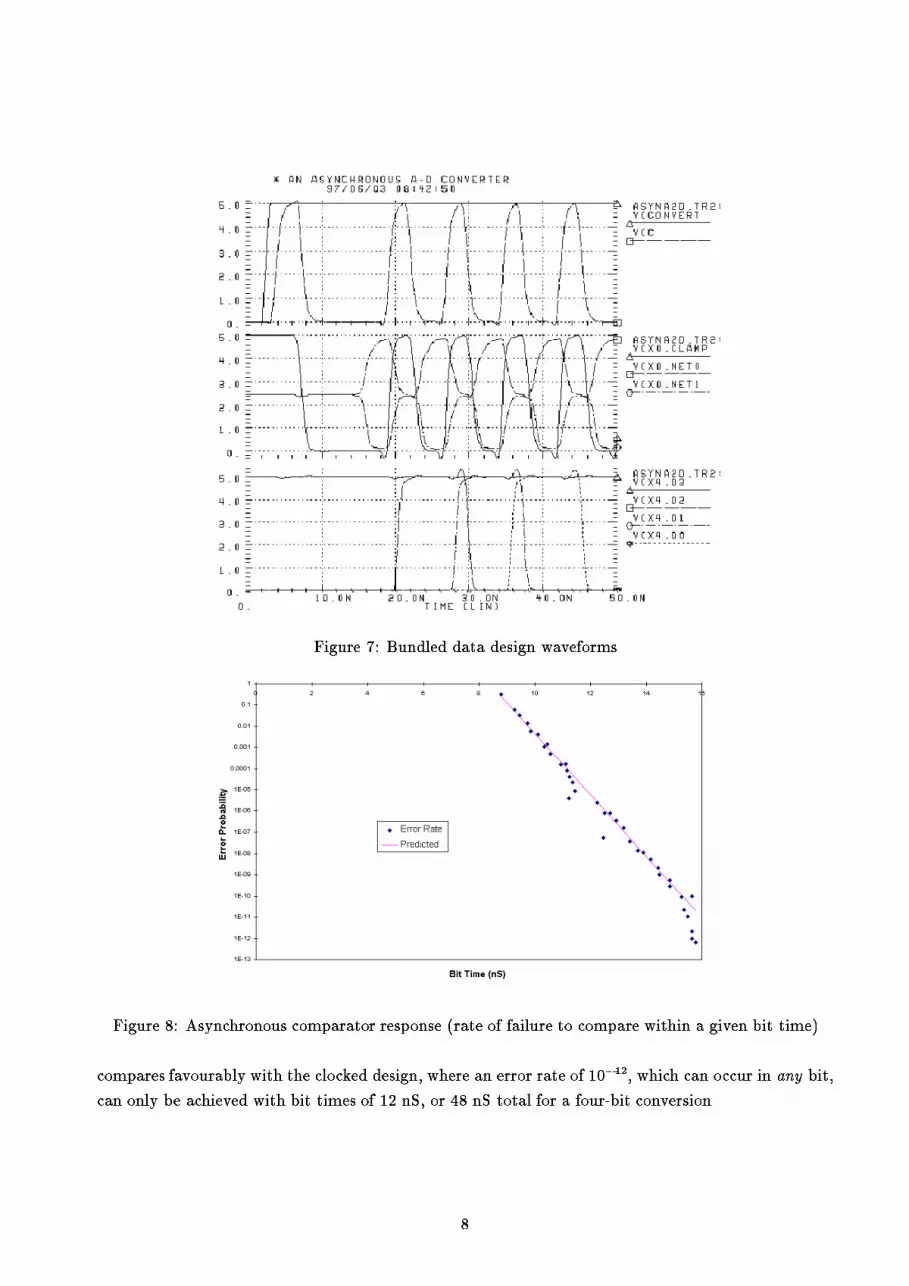
Figure 6: Asynchronous `bundled data' convertershown in Figure 5. The CLAMP is driven from the delayed timing signal edge. This delay is �xed at3.5 nS, allowing for the D-A converter and the �rst stage of the comparator to complete. The overall`bundled data' overheads were 7.35 nS, where the additional delay is needed to compensate for thetime from comparator output to the resetting of the register bit.The system operates essentially in a `bundled data' mode with all state changes linked to the timingsignal. Typical waveforms are shown in Figure 7, which clearly shows the increased time of about 15nS between the �rst and second rising edge of C, resulting from an analog input very close to the D-Aconverter's output given by 1000.Measurements on the time required by the comparator as the di�erence between the analogue inputvoltage and the D-A converter output is varied show that the critical bit time follows fairly closely thefunction: tm = � ln �Vhigh � VlowVm �+ tf ;where �= 0.3 nS, tf = 7.35 nS (the `bundled data' overheads), and Vhigh � Vlow = 5 V.This is shown in Figure 8, where the probability of error is assumed to be determined, as before,by: P = 2(Vhigh � Vlow)LSB e�tm� :The HSPICE modelling of this system gives an average of 32.5 nS for the four bits of a conversion,excluding initialisation of the control loop and outputting the result. The only inaccuracies are now inthe quantisation of the input signal and are con�ned to the least signi�cant bit. The conversion time7
��������������������������������������������������������������������������������������������������������������������������������������������������������������������������������������������������������������������������������������������������������������������������������������������������������������������������������������������������������������������������������������������������������������������������������������������������������������������������������������������������������������������
Figure 7: Bundled data design waveforms ��������������������������������������������������������������������������������������������������������������������������������������������������������������������������������������������������������������������������������������������������������������������������������������������������������������������������������������������������������������������������������������������������������������������������������������������������������������������������������������������������������������������
Figure 8: Asynchronous comparator response (rate of failure to compare within a given bit time)compares favourably with the clocked design, where an error rate of 10�12, which can occur in any bit,can only be achieved with bit times of 12 nS, or 48 nS total for a four-bit conversion.8

3.2 Speed-independent designAn alternative design has been obtained using formal techniques and software [8] available for synthesisof speed-independent circuits. This design uses a more conservative approach to gate delays than the`bundled data' design. Every logic gate in the circuit that implements the successive approximationalgorithmis assumed to have an arbitrary �nite delay. Delay independence guarantees greater reliabilityof the circuit as it: (a) becomes more robust to the parameter variations in the CMOS technology, and(b) allows a design to be implemented without a change on a range of di�erent CMOS technologies.The overall structure for our speed-independent design is shown in Figure 9. It consists of anasynchronous comparator and D-A converter, identical to those used in the `bundled data' design, andfour parts of the speed-independent control logic. The latter include:� A bu�er for intermediate storage of the (one-bit) result of comparison D; D̂; both the inputsD; D̂ and outputs e0; e1 of the bu�er are represented in a dual-rail code with spacer 00. Thecompletion logic of the bu�er produces a CLAMP signal and a signal ea used by the schedulerin determining when to \shift" to the next step in successive approximation.� A register for accumulating the four-bit digital code of the conversion result. The input of theregister consists of the two-rail encoded and bu�ered (e0; e1) value of the comparison result aswell as �ve control signals Li; i = 4; :::; 0, which, respectively, encode (one-hot) the following �vecommands: \Store the initial code 1000", \Store Comparator result in Bit 3, and set Bit 2 tohigh", \Store Comparator result in Bit 2, and set Bit 1 to high", \Store Comparator result inBit 1, and set Bit 0 to high", \Store Comparator result in Bit 0". Thus, the register's data inputis multiplexed. The output of the register consists of the four-bit (dual-rail) digital result (yi; �yi)and a set of four bitwise pre-completion signals (bi).� Completion logic, to produce the global completion signal b from the pre-completion ones andthe command signals.� A scheduler, which controls the execution of the successive approximation algorithm. In doingso, it produces the appropriate controls to the register and signals to the environment with theREADY signal going low (meaning that the converter is initialised with the code 1000) and high(for the completion of the conversion). Those signals are produced at appropriate times from theevents on signals START (from the environment) and ea (from the bu�er).The speed-independent circuit synthesis method we use here is based on the initial speci�cation ofthe control logic behaviour in terms of a Signal Transition Graph (STG) [1]. The latter is a specialisedform of a Petri net [11] whose event nodes are labelled with edges of signals in the speci�ed behaviour.The STG is therefore essentially a formal capture of a timing digram that is used traditionally indigital design. Figure 10 shows an STG that is more condensed (abstract) than the actual model usedfor synthesis of the above-mentioned elements of the converter. It is possible to see in this model theidea of pipelined action. For example, the Compare action (D:=Comp) is done in parallel with theresetting of the register (only, b+, the completion action is shown); the storing in the register (e.g.,Reg:=D3.D2.1.0) is in parallel with the actual clamping of the comparator into spacer (D:=00).9

clamp
VDA
VDA
b
b
y , yi i�
ea
e1
e0
LiLi
�D
D-
Vin+
D/A
ready start
Buffer
Scheduler
Register(with pre-completionlogic)
biCompletionlogic
Figure 9: Speed-independent design (overall system structure)b-
start+
D:=00 D:=Comp
Initialise clamp-
D:=Comp
Bit 3 Compare
b+
clamp+
D:=00
Bit 3 Store
Reg:=D3.1.0.0
clamp-
D:=Comp
Bit 2 Compare
b+
clamp+
clamp+
D:=00
clamp-
D:=Comp
b-b+
Reg:=D3.D2.D1.D0
clamp+
D:=00 D:=Comp
Bit 0 Store
Conversion Completeb+
Bit 0 Compare clamp-
b- Reg:=D3.D2.D1.1
Bit 1 Store clamp+
b+
Bit 1 Compare clamp-
D:=00
Reg:=D3.D2.1.0
b-
Bit 2 Store
b-Reg:=1.0.0.0 start-
ready+
ready-Figure 10: A condensed STG model for speed-independent designThe STG model of the complete circuit would be too large to show in this paper. Furthermore,to obtain logic using petrify, we built separate STGs for the register and the rest of the structure. Inthose STGs we hid the events of the missing part, and thus avoid excessive complexity. One of suchSTGs and the output from petrify are presented in the appendix. The various elements of the circuitare shown in Figures 11 (a) and (b), 12 (a) and (b), and and 13.This design does not completely avoid delay dependence since both the D-A converter and the inputlayer of the comparator are not speed-independent. We believe (after extensive HSPICE experiments)that the delay in the completion logic block and in the bu�er is su�ciently large (at least 10 nS) toallow those delay-dependent parts to complete in coherence with the corresponding change of CLAMP.HSPICE modelling results for the speed-independent design are shown in Figures 14 and 15. The�rst �gure illustrates two examples of comparator response to the falling edge of CLAMP, one withmetastability (lasting nearly 4 nS), when the input analogue voltage is near to the nearest LSB line,and the other without. The second waveform shows how the most critical groups of signals behaveduring conversion. Similar to the bundled data design, we used the same example { converting thevalue whose code is close to the mid-range point (between 0111 and 1000). A one-bit conversion cycleis about 45 nS, which is about �ve times that of the bundled data design. The critical cycle is obviouslyvia the following components: bu�er, scheduler, register and completion logic. Note that the circuitoperates with a four-phase self-timed protocol. There is a slight di�erence between the phases, wherethe phases during which the value is stored in the register (when both the register latches and the10

C
eaclamp
e0
e1
b
D
C�D (a) e1
e0
Li+1
Li
start
yi
bi
�yi
(b)Figure 11: Speed-independent design: (a) bu�er circuit, and (b) register and pre-completion logic (i-thbit, i=1,2)start
ea
ready
x0x3 x4
x4
L0 (a) ea
Li
xi−1 xixi+1
xi
Li+1 (b)Figure 12: Speed-independent design: scheduler; (a) initialisation control element (producing L4 =READY), and (b) i-th bit control element (for Li; i = 0; 1; 2; 3)completion logic are working) are 3-5 nS longer than the phases when only the completion logic isin action. Thus, the time 20 nS (for one of those phase pairs) is approximately divided between theelements of the circuit in the following way: bu�er 3 nS, scheduler 6 nS, pre-completion logic 5 nS andcompletion logic 6 nS.3.3 Exploring other speed-independent design optionsIn addition to the above-mentioned design (SI-1) we also produced two other speed-independent designswith slightly di�erent approach to synthesis of control logic. One of them (SI-2) used a more canonicaltype of register consisting of a row of four self-timed master-slave ip- ops that was designed usingthe idea from [12], Fig.4.11 (b)). The SI-2 design also included a completion circuit, a commandscheduler (similar to the one above) and an additional synchronisation logic. The use of a master-slaveregister allowed us to avoid putting an additional bu�er between the comparator and register, but atthe cost of extra size (the full row of masters). The synchronisation logic we used also provided a moreconventional handshaking with the environment { the READY signal would only go high after theentire conversion cycle (with the initialisation phase being part thereof). As a result, the SI-2 design11

L0L1L2b2L3b2b2 b1b1b1 b0b0b0 b3b3
bC
b2 b1 b0b3Figure 13: Speed-independent design: completion logicFigure 14: Comparator response with and without metastabilityFigure 15: Speed-independent design: conversion waveforms12

was more modular, and the parts of logic that had to be synthesised with petrify were simpler. Thepayment for these bene�ts was overall slower operation, with the one-bit conversion cycle being about60 nS.The third design (SI-3) was on the other hand a more specialised than SI-1. For example, bit-selection was part of the functionality of the register, thus eliminating the need for a separate scheduler.The advantages of this approach, where the register acted as a multiplexing state machine, were lesscircuit size and overall faster operation. The one-bit cycle could be reduced down to 30 nS (reducing itfurther to the level of that of the \bundled data" design would require eliminating completion logic andputting more stringent conditions on relative delays). The main shortcomings of such a less structureddesign were: (i) that synthesis with petrify was at its complexity limit (total number of signals in theSTGs up to 40); (ii) that the design of the register logic was no longer scalable (from four bit to n-bitconverter).We thus believe that among those three speed-independent options the SI-1 design would be optimalin modularity, speed and e�ciency. It should also be relatively easy to test due to its modularity andself-checking properties of speed-independent circuits.4 Comparison of synchronous and asynchronous A-D convertersFigure 4 shows that the synchronous converter can be clocked with a bit time as low as 5 nS if errorrates of 10�4 are acceptable. The design of the bundled data converter is similar, with the exceptionof the comparator circuit, and the timing signal generation, yet it requires at least 8 nS to make acomparison. This is because the bistable circuit used is not active until the clamp signal goes low,and this delay is �xed at 3.5 nS after the register change. Additionally, a time of 3.85 nS is requiredfrom the time metastability is resolved in the bistable to generate the next clock. In the synchronoussystem, the only timing signal is the clock, and therefore register changes are communicated to the D-Aconverter, and hence the comparator, immediately. Similarly, the next clock edge is not determinedby the comparator output.If the converter is used in a real-time application, where a control loop or some other system iscritically dependent on the receipt of accurate data within a given time, the unbounded conversiontime of the asynchronous system may cause errors even though the data is accurate. We have simplyexchanged uncertainty in data for uncertainty in time.An advantageous compromise can be achieved by terminating the conversion process at a �xedtime, and accepting the current value of the output register whether metastability exists or not. Thusif 42 nS is allowed for the four-bit comparisons, a worst case time for the fastest three bits is 24.26 nS,leaving 17.74 nS for the worst bit. This would give a probability of error of less than 10�12, which canonly be matched by a synchronous converter with a time of 48 nS for the four comparisons. Over therange 42 { 47 nS, the bounded asynchronous design is both faster and more reliable than a synchronousconverter because the clock rate does not need to be �xed at the time for the slowest comparison. Inconverters with 8 or 12 bits, the improvements will be greater.Another advantage of bounded asynchronous timing is that errors are less likely to be severe. Theprobability of error in a particular bit, and no higher bit, in a successive approximation synchronousconverter, is the same as the probability of the comparison at that time being longer than tb and not13

earlier. This depends on the probability of the analog input being closer than Vm to the D-A output,where Vm = (Vhigh�Vlow )e�tb� as before. For the least signi�cant bit, that probability is P = VmLSB , andfor bit n it is P = 2�nVmLSB 1.The probability of the n-th bit comparison taking longer than tb is therefore:P = 2�n(Vhigh � Vlow)LSB e�tb� :If we assume that only one bit comparison in an asynchronous converter can cause metastability,and that the others take a time tb, the most signi�cant bit can take the full conversion time, say, 4tb,before being terminated, the second 3tb, so that the probability of error in the high order bits where nis large is much less than later bits. In general the probability of error in a particular bit will now be:P = 2�n(Vhigh � Vlow)LSB e�(n+1)tb� :this gives a probability of error in the most signi�cant bit of less than 10�47 for the four bit boundedtime asynchronous converter compared with a �gure of about 10�20 for the asynchronous converter.Obviously, comparison of a speed-independent converter, which is signi�cantly slower than thebundled data one, would be more di�cult to perform in numerical terms. On the other hand, speed-independent designs should not be considered only out of theoretical interest if one had to take intoaccount other risk factors besides metastability, such as delay variations of CMOS submicron technologyand the need to maintain portability of the design. This however takes us beyond the scope of thepaper.5 ConclusionsWe have shown that analogue to digital converters with a �xed conversion time are subject to errors dueto metastability. These errors will occur in all converter designs with a bounded time for decisions,and are potentially severe. It is also clear that an asynchronous design can be more reliable, andfaster, on average, than a synchronous design but its completion time may be in�nite. Two types ofasynchronous converters have been described, the design of the �rst follows a 'bundled data' approachin which there is a single timing path whose delays are matched with the data path delays, and thesecond is a totally self-timed (only the D-A converter part is assumed to have bounded delay, quitesu�cient in practice) system, which is insensitive to variations in individual component delays. It isclear from the �rst design that a reliable asynchronous conversion could be completed in under the 10nS per bit required by the synchronous design with an error rate of 10�11. The fully self-timed designcan be more portable and robust because it does not assume that gate delays on the same chip will havesimilar delays, but has at least twice as many transistors and typically takes three-four times longerperiod for a conversion than the bundled data one. Such a signi�cant slow-down is caused mainlyby the requirement of explicit acknowledgement of signal tranistions for speed-independent operation,and as a result, use of additional hardware (completion logic). It is interesting to note that while theasynchronous designs will not produce an error of more than one bit in the result, the conversion time1The integral value of this probability through all bits can be estimated as the sum of the series of P = 2�iVmLSB ; i =0; :::;n, which tends to P = 2VmLSB as n goes to in�nity. This last formula was used in Section 2.3.14

is not predictable, and this may cause di�culties in a real time system. This problem is linked tothe process of conversion between reals and integers, and the limited gain - bandwidth of all physicaldevices used as comparators.References[1] T.-A. CHU and L.A. GLASSER, \Synthesis of Self-Timed Control Circuits from Graphs: AnExample", IEEE International Conference on Computer Design (ICCD86), 1986, pp.565 { 571.[2] T.J.CHANEY and C.E.MOLNAR, \Anomalous behavior of synchronizer and arbiter circuits",IEEE Transactions on Computers , C-22(4), pp. 412{422, April 1973.[3] D.J.KINNIMENT and J.V.WOODS, \Synchronisation and arbitration circuits in digital systems",Proceedings IEE , vol 123, No. 10, pp. 961{966, October 1976.[4] B. RUSSELL, Introduction to Mathematical Philosophy , London, G.Allen and Unwin, 1920 (pp.84 { 86).[5] M. MENDLER and T. STROUP, \Newtonian arbiters cannot be proven correct", Formal Methodsin System Design, 3(3), pp. 233-257, December 1993.[6] I. M. MITCHELL and M.R. GREENSTREET, \Proving Newtonian Arbiters Correct, almostsurely", Proc. of Conf. on Designing Correct Circuits (DCC'96), 1996 (see also: IAN M.MITCHELL, \Proving Newtonian Arbiters Correct, Almost Surely", MSc Thesis, University ofBritish Columbia, October 1996).[7] C. L. SEITZ, \System Timing"; In C. Mead and L. Conway, Introduction to VLSI Systems ,Chapter 7, pp.218{262, Addison Wesley 1979.[8] J. CORTADELLA, A. KONDRATYEV, M. KISHINEVSKY, L. LAVAGNO and A. YAKOVLEV,Petrify: a tool for manipulating concurrent speci�cations and synthesis of asynchronous con-trollers, Proc. 11th Conference on Design of Integrated Circuits and Systems (DCIS'96),Barcelona, Nov. 1996, pp.205-210.[9] H.J.M. VEENDRICK, \The behaviour of ip- ops used as synchronizers and prediction of theirfailure rate", IEEE Journal of Solid-State Circuits , vol. SC-15(2), pp. 169{176, April 1980.[10] D.J. KINNIMENT, A.V. YAKOVLEV, and B. GAO, \Metastable Behaviour in Arbiter Circuits",Technical Report Number: 604, Dept. of Computing Science, University of Newcastle upon Tyne1997.[11] T. MURATA, \Petri nets: properties, analysis and applications",Proceedings of IEEE , vol. 77(4),pp. 541{580, April 1989.[12] V. VARSHAVSKY, M. KISHINEVSKY, V. MARAKHOVSKY, V. PESCHANSKY, L. ROSEN-BLUM, A. TAUBIN, and B. TSIRLIN, Self-Timed Control of Concurrent Processes , Kluwer Aca-demic Publishers, Dordrecht, 1990 (Russian Edition: Nauka, Moscow, 1986).15

ready+
b-
x3+
er-
ready-
b+
x4-
ea-
x0-
clamp-
er+
l3+
d+ ea+
d-
clamp+
clamp+
d-
ea+
b-
x2+
ea-
d+
er+
er-
l3-
b+l0-
clamp-
x4+
clamp-
d+
ea-
b+
x3-
ea+
d-
er-
er+
l2+
b-l0+
clamp+
x1-
clamp+
d-
ea+
b-
x1+
ea-
d+
er+
er-l2-
b+l1-
clamp-
x0+
clamp-
d+
ea-
b+
x2-
ea+
d-
er-
er+
l1+b-
clamp+Figure 16: STG speci�cation for schedulerAppendix: Signal Transition Graphs and synthesis results from Petrify 2The STG used to synthesise the schedule logic is shown in Figure 16. It was built automatically (bytool draw.astg) from the designer's textual speci�cation. This STG hides the details of the bu�er,register and completion logic { one can observe that only the completion signals b, from the register,and ea, from the bu�er, are used. Signals xi are used to resolve coding con icts and act as internalmemory of the scheduler. Their transitions are organised in parallel with the main events in order tominimise the critical cycle delay.The output from petrify is shown below:# EQN file for model AD_control_buffer_top1# Generated by petrify 3.3 (compiled 6-Sep-97 at 9:33 AM)# Outputs between brackets "[out]" indicate a feedback to input "out"# Estimated area = 68.00INORDER = ready l3 l2 l1 l0 b clamp er ea d x1 x2 x3 x4 x0;OUTORDER = [ready] [l3] [l2] [l1] [l0] [b] [clamp] [er] [ea][d] [x1] [x2] [x3] [x4] [x0];[ready] = x3' (clamp x4 x0' + ready) + ready clamp;[l3] = x2' (clamp x3 x4' + l3) + l3 clamp;[l2] = x1' (clamp x3' x2 + l2) + l2 clamp;[l1] = clamp x1 x2' x0' + l1 (x0' + clamp);[l0] = clamp x1' x4' x0 + l0 (x4' + clamp);[b] = l3' ready' l0' l1' l2';[clamp] = ea;[er] = b;[ea] = er (ea + d) + ea d;[d] = clamp';[x1] = x0' x1 + l2 + l1;[x2] = x2 x1' + l2 + l3;[x3] = x3 x2' + ready + l3;[x4] = x3' x4 + l0 + ready;[x0] = x4' x0 + l1 + l0;Another example is the STG, shown in Fig 17, specifying the register together with its pre-completion logic.The details of the surrounding logic, such as scheduler, are again hidden inside the handshakes between thecompletion signals b, outputs of the bu�er (e0; e1) and controls ready; l3 ; :::; l0 .The output from petrify is shown below:2 included to help reviewing; can be omited in the �nal version.16

ready+ y30^0
y21^0
y11^0
y01^0
y31^1
y20^1
y10^1
y00^1
b3+
b2+
b1+
b0+
b- e0-
e1-
ready-
e0+
b3-
b2-
b1-
b0-
e1+
b+e0+
e1+
b+
y31^0
e0-
y30^0
e1-
l3+
b0-
y20^0
l0-
y21^1
y30^1
y31^1
b2+
e0-
e1-
b-
b3+
b- b0+ y00^1
y01^1
y01^0
y00^0
l3-b3-
b2-
l0+
b+
e0+
e1+
e0+
e1+
y21^0
e0-
y20^0
e1-
b+
l2+
b1-
b0-
y10^0
l1-
y11^1
y20^1
y21^1
b1+
e0-
e1-
b-
b2+
b-b1+
b0+ y01^1 y00^0
y10^1
y11^1
y11^0
y10^0
l2-
b2-
b1-
l1+
b+
e0+
e1+Figure 17: STG speci�cation for register# EQN file for model AD_control_buffer_latch1# Generated by petrify 3.3 (compiled 6-Sep-97 at 9:33 AM)# Outputs between brackets "[out]" indicate a feedback to input "out"# Estimated area = 68.00INORDER = e0 e1 ready l3 l2 l1 l0 b0 b1 b2 b3 b y30 y31 y20 y21 y10 y11 y00 y01;OUTORDER = [b0] [b1] [b2] [b3] [b] [y30] [y31] [y20] [y21] [y10] [y11] [y00][y01];[b0] = l0 (e1 + y00 + b0) + l1 y01 + ready y00;[b1] = l1 (b1 + y10 + e1) + l2 y11 + ready y10;[b2] = l2 (y20 + b2 + e1) + l3 y21 + ready y20;[b3] = l3 (e1 + b3 + y30) + ready y31;[b] = l0' b (l1' b2' + l3' b1') + b3' (l3 + ready) + b0' (b3' b2' b1' +ready + l1);[y30] = y31' ready';[y31] = y30' (l3' + e0');[y20] = y21' l3';[y21] = ready' y20' (e0' + l2');[y10] = l2' y11';[y11] = ready' y10' (l1' + e0');[y00] = y01' l1';[y01] = ready' y00' (l0' + e0');17