the promise of halide double perovskites - stanford university
TRANSCRIPT
Double Perovskites
Doubling the Stakes: The Promise of Halide DoublePerovskitesNathan R. Wolf+, Bridget A. Connor+, Adam H. Slavney, andHemamala I. Karunadasa*
AngewandteChemie
Keywords:band structure ·double perovskites ·perovskites ·photovoltaics ·semiconductors
Dedicated to Prof. Harry B. Gray onthe occasion of his 85th birthday
AngewandteChemieMinireviews
How to cite:International Edition: doi.org/10.1002/anie.202016185German Edition: doi.org/10.1002/ange.202016185
2 � 2021 Wiley-VCH GmbH Angew. Chem. Int. Ed. 2021, 60, 2 – 17� �
These are not the final page numbers!
1. Introduction
Halide perovskites, which date back to the 1800s,[1] arecrystalline semiconductors formed in solution-state or mildsolid-state reactions. These ionic solids consist of anionicmetal-halide octahedra connected in 0, 1, 2, or 3 dimensionsthrough shared corners, with inorganic or organic cationsproviding charge compensation. Research efforts on three-dimensional (3D) lead-halide perovskites have recently beeninvigorated due to the remarkable rise in the efficiencies ofsolar cells employing these materials as absorbers, specifically,(MA)PbI3 (MA = CH3NH3
+)[2] and its derivatives.[3] How-ever, lead perovskites constitute only a small section of thevast and diverse family of halide perovskites. Thus, morerecently, researchers have sought to cast a wider net in searchof new compositions that mimic the optoelectronic propertiesof the lead perovskites.[4] These efforts seek to both under-stand the origin of the remarkable optoelectronic propertiesof lead perovskites through fundamental studies and toidentify functional analogues with improved stability as wellas reduced toxicity and environmental impact.[4a] Of all thealternatives that have been explored, the A2BB’X6 (A =
monocation, X = halide) double perovskites have emergedas the most abundant and promising family.[5] Doubleperovskites maintain a similar structural framework to thatfound in single perovskites while permitting a wider variety ofcations to be incorporated into the octahedrally coordinatedB/B’ site. This enables access to an expansive range ofalternative compositions and electronic structures, whichresearchers are only beginning to explore.
Herein, we discuss select structural and optoelectronictopics relevant to contemporary research on halide doubleperovskites. This Minireview will not address nanostructur-ing[6] nor detail device applications,[7] except for a briefdiscussion of the latter in the concluding section. In Section 1,we define double perovskites and briefly survey their history.Section 2 discusses different subclasses of double perovskites,including their two-dimensional (2D) variants and the localstructural distortions that occur in these materials. Section 3gives an overview of double perovskite electronic structures
and highlights simple rules that predictthe electronic structures of undiscov-ered compounds. In Section 4, we de-tail strategies for modifying the elec-tronic structure. We conclude in Sec-tion 5 by emphasizing commonalitiesbetween double perovskites and otherwell-known materials families, whichwe hope will provide direction forfuture studies.
1.1. Definition of 3D Double Perovskites
As a materials family with a long,rich history, double perovskites haveacquired various definitions, which arethe subject of continuing discussion.[8]
For the purposes of this Minireview,we follow a relatively restrictive definition of 3D halidedouble perovskites by including only materials that meet thefollowing criteria:1. The structure contains cations or vacancies surrounded by
six halides ([BX6]n� ; B = cation or vacancy; X = halide).
2. The [BX6]n� units are exclusively corner-sharing in a 3D
pattern (B = cation or vacancy; X = halide).3. There are exactly two structurally distinguishable [BX6]
n�
motifs in the unit cell, such that the chemical formula mustbe A2BB’X6 (B = cation or vacancy; X = halide).
The third criterion, requiring exactly two distinct [BX6]n�
units, distinguishes double perovskites from single perov-skites (Figure 1). The ordering of these distinct [BX6]
n� unitssignificantly impacts the material�s electronic structure (seeSection 3).[9] Fully disordered alloys with only one distinct Bsite, such as A(Pb1�xSnx)X3 (which were investigated as earlyas the 1970s[10] and recently used in solar cells[11]) are thusclassified as single perovskites. In the oxide literature,materials with two distinct, ordered A sites (AA’B2X6) arecommonly considered double perovskites.[12] We exclude suchcompositions from our definition because examples of A-siteordered halide perovskites are extremely rare[13] and becausesuch materials are expected to exhibit optoelectronic proper-ties more similar to those of single perovskites (see Sec-tion 3.1).
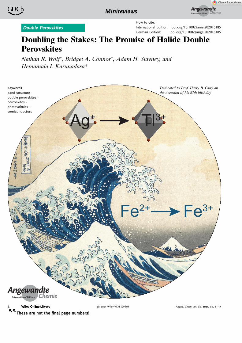
When the stakes are doubled in a wager, a player must correctly placetwo consecutive bets to win, but the payout is larger. Similarly, two Bsites in combination dictate the properties of A2BB’X6 (A = mono-cation, X = halide) double perovskites. Correctly picking two B sites ismore challenging than picking just one, as in the AIBIIX3 singleperovskites, but the options are greater and, we believe, the rewards arehigher when the stakes are doubled. In this Minireview, we emphasizefundamental aspects of halide double perovskites to provide a foun-dation for interested readers to explore this extraordinary class ofmaterials. In particular, we highlight the differences and similaritiesbetween double and single perovskites and describe how the doubleperovskite structure potentially offers greater control over photo-physical properties.
[*] N. R. Wolf,[+] Dr. B. A. Connor,[+] Dr. A. H. Slavney,Prof. H. I. KarunadasaDepartment of Chemistry, Stanford UniversityStanford, California 94305 (USA)
Prof. H. I. KarunadasaStanford Institute for Materials and Energy SciencesSLAC National Accelerator LaboratoryMenlo Park, California 94025 (USA)E-mail: [email protected]
[+] These authors contributed equally to this work.
The ORCID identification numbers for the authors of this article canbe found under: https://doi.org/10.1002/anie.202016185.
AngewandteChemieMinireviews
3Angew. Chem. Int. Ed. 2021, 60, 2 – 17 � 2021 Wiley-VCH GmbH www.angewandte.org
These are not the final page numbers! � �
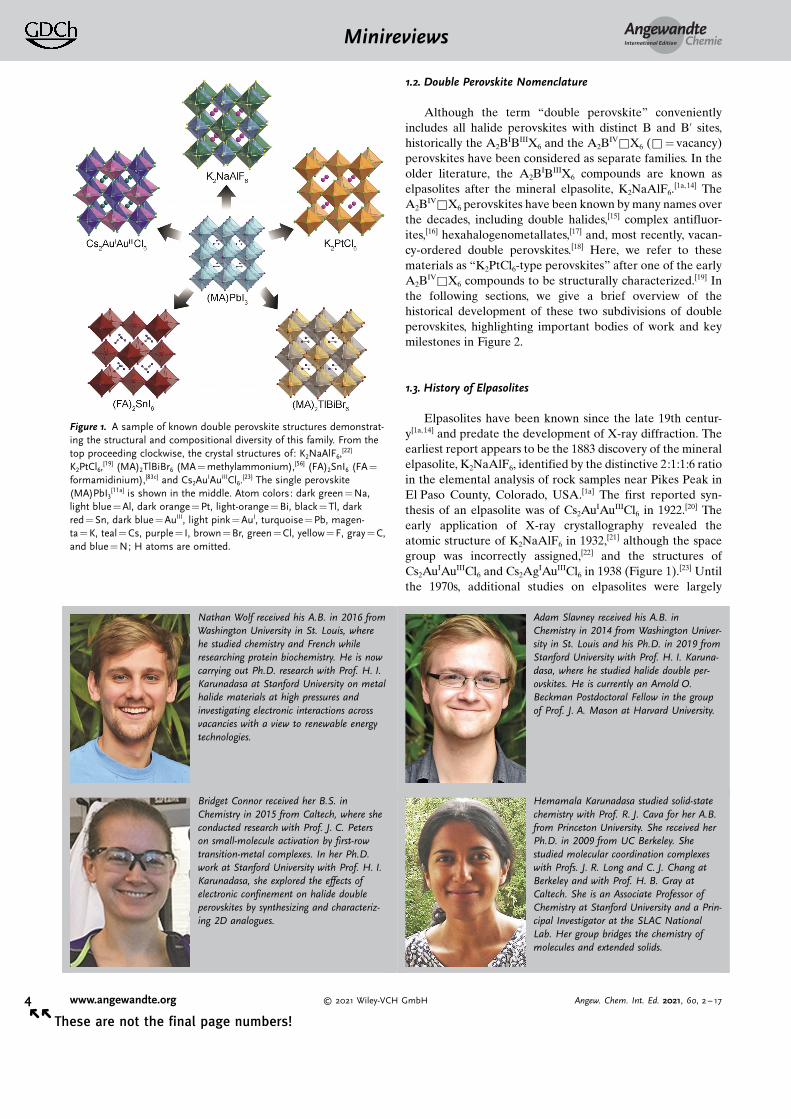
1.2. Double Perovskite Nomenclature
Although the term “double perovskite” convenientlyincludes all halide perovskites with distinct B and B’ sites,historically the A2B
IBIIIX6 and the A2BIV&X6 (&= vacancy)
perovskites have been considered as separate families. In theolder literature, the A2B
IBIIIX6 compounds are known aselpasolites after the mineral elpasolite, K2NaAlF6.
[1a,14] TheA2B
IV&X6 perovskites have been known by many names overthe decades, including double halides,[15] complex antifluor-ites,[16] hexahalogenometallates,[17] and, most recently, vacan-cy-ordered double perovskites.[18] Here, we refer to thesematerials as “K2PtCl6-type perovskites” after one of the earlyA2B
IV&X6 compounds to be structurally characterized.[19] Inthe following sections, we give a brief overview of thehistorical development of these two subdivisions of doubleperovskites, highlighting important bodies of work and keymilestones in Figure 2.
1.3. History of Elpasolites
Elpasolites have been known since the late 19th centur-y[1a, 14] and predate the development of X-ray diffraction. Theearliest report appears to be the 1883 discovery of the mineralelpasolite, K2NaAlF6, identified by the distinctive 2:1:1:6 ratioin the elemental analysis of rock samples near Pikes Peak inEl Paso County, Colorado, USA.[1a] The first reported syn-thesis of an elpasolite was of Cs2AuIAuIIICl6 in 1922.[20] Theearly application of X-ray crystallography revealed theatomic structure of K2NaAlF6 in 1932,[21] although the spacegroup was incorrectly assigned,[22] and the structures ofCs2AuIAuIIICl6 and Cs2AgIAuIIICl6 in 1938 (Figure 1).[23] Untilthe 1970s, additional studies on elpasolites were largely
Nathan Wolf received his A.B. in 2016 fromWashington University in St. Louis, wherehe studied chemistry and French whileresearching protein biochemistry. He is nowcarrying out Ph.D. research with Prof. H. I.Karunadasa at Stanford University on metalhalide materials at high pressures andinvestigating electronic interactions acrossvacancies with a view to renewable energytechnologies.
Bridget Connor received her B.S. inChemistry in 2015 from Caltech, where sheconducted research with Prof. J. C. Peterson small-molecule activation by first-rowtransition-metal complexes. In her Ph.D.work at Stanford University with Prof. H. I.Karunadasa, she explored the effects ofelectronic confinement on halide doubleperovskites by synthesizing and characteriz-ing 2D analogues.
Adam Slavney received his A.B. inChemistry in 2014 from Washington Univer-sity in St. Louis and his Ph.D. in 2019 fromStanford University with Prof. H. I. Karuna-dasa, where he studied halide double per-ovskites. He is currently an Arnold O.Beckman Postdoctoral Fellow in the groupof Prof. J. A. Mason at Harvard University.
Hemamala Karunadasa studied solid-statechemistry with Prof. R. J. Cava for her A.B.from Princeton University. She received herPh.D. in 2009 from UC Berkeley. Shestudied molecular coordination complexeswith Profs. J. R. Long and C. J. Chang atBerkeley and with Prof. H. B. Gray atCaltech. She is an Associate Professor ofChemistry at Stanford University and a Prin-cipal Investigator at the SLAC NationalLab. Her group bridges the chemistry ofmolecules and extended solids.
Figure 1. A sample of known double perovskite structures demonstrat-ing the structural and compositional diversity of this family. From thetop proceeding clockwise, the crystal structures of: K2NaAlF6,
[22]
K2PtCl6,[19] (MA)2TlBiBr6 (MA = methylammonium),[56] (FA)2SnI6 (FA =
formamidinium),[83c] and Cs2AuIAuIIICl6.[23] The single perovskite
(MA)PbI3[11a] is shown in the middle. Atom colors: dark green = Na,
light blue= Al, dark orange=Pt, light-orange=Bi, black =Tl, darkred = Sn, dark blue = AuIII, light pink = AuI, turquoise=Pb, magen-ta = K, teal = Cs, purple= I, brown=Br, green =Cl, yellow=F, gray= C,and blue = N; H atoms are omitted.
AngewandteChemieMinireviews
4 www.angewandte.org � 2021 Wiley-VCH GmbH Angew. Chem. Int. Ed. 2021, 60, 2 – 17� �
These are not the final page numbers!
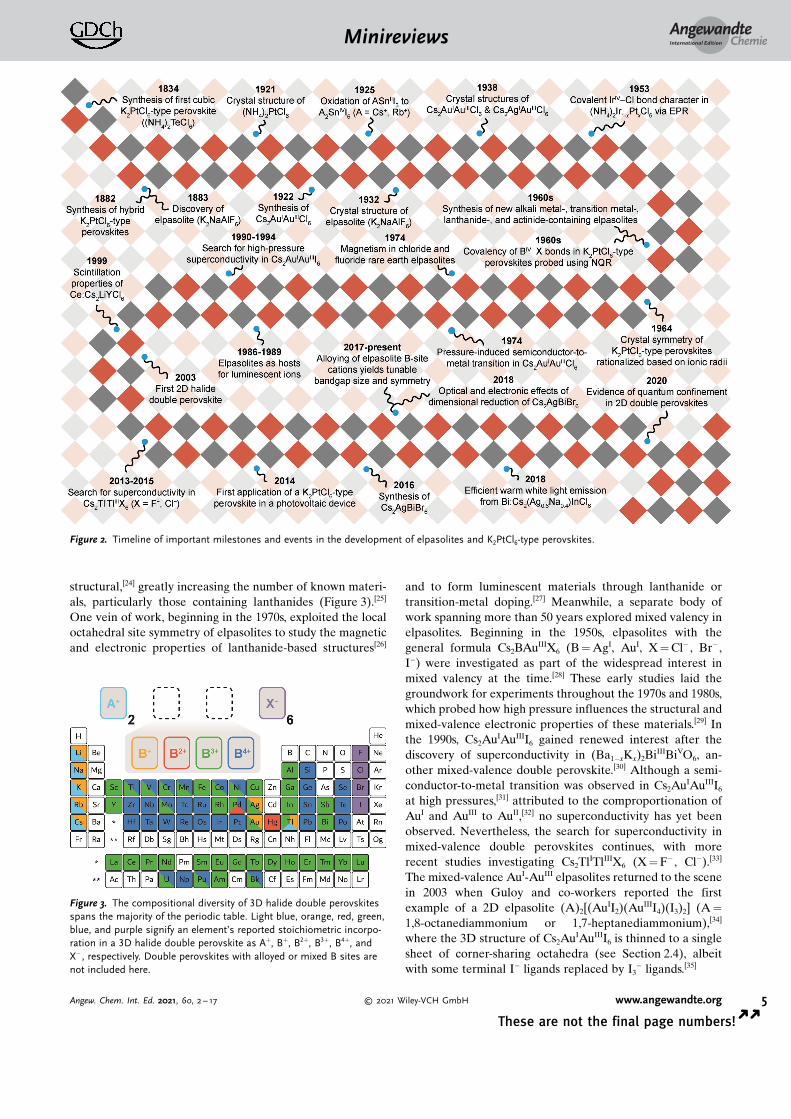
structural,[24] greatly increasing the number of known materi-als, particularly those containing lanthanides (Figure 3).[25]
One vein of work, beginning in the 1970s, exploited the localoctahedral site symmetry of elpasolites to study the magneticand electronic properties of lanthanide-based structures[26]
and to form luminescent materials through lanthanide ortransition-metal doping.[27] Meanwhile, a separate body ofwork spanning more than 50 years explored mixed valency inelpasolites. Beginning in the 1950s, elpasolites with thegeneral formula Cs2BAuIIIX6 (B = AgI, AuI, X = Cl� , Br� ,I�) were investigated as part of the widespread interest inmixed valency at the time.[28] These early studies laid thegroundwork for experiments throughout the 1970s and 1980s,which probed how high pressure influences the structural andmixed-valence electronic properties of these materials.[29] Inthe 1990s, Cs2AuIAuIIII6 gained renewed interest after thediscovery of superconductivity in (Ba1�xKx)2BiIIIBiVO6, an-other mixed-valence double perovskite.[30] Although a semi-conductor-to-metal transition was observed in Cs2AuIAuIIII6
at high pressures,[31] attributed to the comproportionation ofAuI and AuIII to AuII,[32] no superconductivity has yet beenobserved. Nevertheless, the search for superconductivity inmixed-valence double perovskites continues, with morerecent studies investigating Cs2TlITlIIIX6 (X = F� , Cl�).[33]
The mixed-valence AuI-AuIII elpasolites returned to the scenein 2003 when Guloy and co-workers reported the firstexample of a 2D elpasolite (A)2[(AuII2)(AuIIII4)(I3)2] (A =
1,8-octanediammonium or 1,7-heptanediammonium),[34]
where the 3D structure of Cs2AuIAuIIII6 is thinned to a singlesheet of corner-sharing octahedra (see Section 2.4), albeitwith some terminal I� ligands replaced by I3
� ligands.[35]
Figure 2. Timeline of important milestones and events in the development of elpasolites and K2PtCl6-type perovskites.
Figure 3. The compositional diversity of 3D halide double perovskitesspans the majority of the periodic table. Light blue, orange, red, green,blue, and purple signify an element’s reported stoichiometric incorpo-ration in a 3D halide double perovskite as A+, B+, B2+, B3+, B4+, andX� , respectively. Double perovskites with alloyed or mixed B sites arenot included here.
AngewandteChemieMinireviews
5Angew. Chem. Int. Ed. 2021, 60, 2 – 17 � 2021 Wiley-VCH GmbH www.angewandte.org
These are not the final page numbers! � �
1.4. History of K2PtCl6-Type Perovskites
The origin of K2PtCl6-type perovskites dates back to thesynthesis of A2TeX6 (A = K+, Na+, NH4
+ and X = Cl� , Br� ,I�) in 1834.[36] Before the 1920s, studies focused on synthesis,elemental analysis, and crystal morphology.[15, 37] Large organ-ic cations were commonly employed as A-site cations, thusdemonstrating the close association of K2PtCl6-type perov-skites with molecular salts.[37b,d,38] A series of X-ray crystallo-graphic studies in the 1920s showed that these materialsconsist of isolated octahedra (Figure 1).[19, 39] The authorsimmediately recognized the similarity to the CaF2 fluoritestructure, where PtCl6
2� replaces Ca2+ and K+ replaces F�
(Figure 4A,B), thereby leading to their classification asantifluorites. Many more K2PtCl6-type perovskites weresubsequently characterized,[40] and at least 30 elements havebeen incorporated at the B site to date (Figure 3).[41] Anumber of these materials exhibit symmetry-lowering octa-hedral rotations as a result of over- or undersized A-sitecations (see Section 2.5.2).[42] A structural analysis, similar tothe Goldschmidt tolerance factor,[43] was first developed in1964 by Brown, which enabled prediction of cubic K2PtCl6-type perovskites and rationalized their temperature-depen-dent phase-change behavior.[42, 44] The rapid diversification ofthe K2PtCl6-type perovskites led to a growing interest in theirfundamental properties. Throughout the 1960s, these materi-als were used to investigate the covalency of the metal-halidebond of [BX6]
2� octahedral complexes (particularly for B =
third-row transition metal) using pure quadrupole resonancespectroscopy.[45] Additionally, much like elpasolites, K2PtCl6-type perovskites were found to be excellent host structures formetal alloying, facilitating the discovery of covalent p-bonding in IrCl6
2� by electron paramagnetic resonancespectroscopy,[46] charge transfer between mixed-valence SbIII
and SbV ions by optical spectroscopy,[47] and photon upcon-version from Re4+ ions doped into a Cs2ZrCl6 host struc-ture.[27d, 48]
1.5. Recent Work
The recent revival of interest in halide double perovskitesoriginates from the search for nontoxic alternatives toAPbIIX3 in perovskite photovoltaics.[4a] The first commentson the K2PtCl6-type perovskites in recent perovskite litera-ture arose from the known[49] undesired oxidation of ASnIII3
to A2SnIVI6,[11a,50] followed by a 2014 investigation of Cs2SnI6
for photovoltaic applications.[7b] The following year, a compu-tational paper proposed the hypothetical elpasolite(MA)2TlBiI6 as a potential photovoltaic absorber.[51] Thisearly work did not refer to the subject materials as doubleperovskites. Recognition of the potential of the halide doubleperovskite family as a whole arrived in 2016, when threegroups independently reported the synthesis and optoelec-tronic properties of the elpasolites Cs2AgBiX6 (X = Cl� and/or Br�).[52] Since then, many new elpasolites have beensynthesized, including Cs2AgInCl6,
[53] Cs2AgTlX6 (X = Cl� ,Br�),[54] Cs2AgSbCl6,
[55] (MA)2TlBiBr6,[56] and various al-
loys.[55,57] This recent growth of novel elpasolite compositionshas sparked an interest in many K2PtCl6-type perovskiteswell-known in the early literature, such as Cs2TeI6,
[15]
Cs2PdBr6,[37c] Cs2SnI6,
[58] Cs2PtI6,[59] and Cs2TiI6,
[60] as research-ers reinvestigate these materials in the context of photo-voltaics.[18, 61] The recent interest in halide double perovskitesas photovoltaic absorbers has led to new applications forthese materials[7] while also serving as a platform for morefundamental studies, such as investigations into the conse-quences of dimensional reduction.[62] In particular, a recentflurry of reports has increased the phase space of 2Delpasolites, starting with Ag-Bi in 2018[62a] and then expandingto Ag-Tl,[62b] Ag-In,[62c] and Cu-Bi.[62d] The young, but rapidlygrowing, field of lower-dimensional double perovskites islikely to greatly expand the structural and functional diversityof the double perovskite family in the coming years, aswitnessed previously for the halide single perovskites.[63]
2. A Structural Survey
In the following sections, we discuss some of the mostimportant aspects of the double perovskite structure, includ-ing B-site ordering, dimensional reduction, and structuraldistortion.
2.1. Thermodynamics of B-Site Ordering
B-site ordering distinguishes double perovskites fromsingle perovskites. In halide double perovskites, this orderingis thermodynamically favored. For example, the completedisordering of the Ag+ and Bi3+ cations in Cs2AgBiBr6 iscalculated to occur only above 3000 K.[64] At room temper-ature, entropically driven B-site disordering is likely presentbut only at such low levels that it is better discussed asa propensity for the formation of anti-site defects.[65] Similarto the case of the oxide perovskites, B-site ordering is likelydriven by electrostatics, as having adjacent 3 + or 4 + cationsis unfavorable.[8a,b] Indeed, isovalent B and B’ cations most
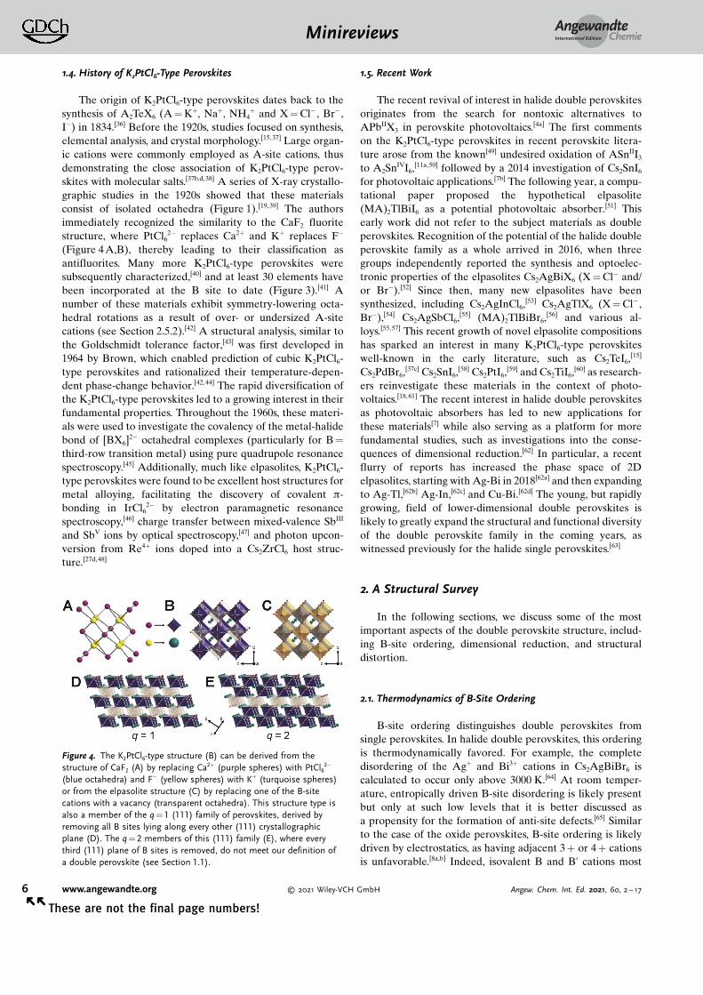
Figure 4. The K2PtCl6-type structure (B) can be derived from thestructure of CaF2 (A) by replacing Ca2+ (purple spheres) with PtCl6
2�
(blue octahedra) and F� (yellow spheres) with K+ (turquoise spheres)or from the elpasolite structure (C) by replacing one of the B-sitecations with a vacancy (transparent octahedra). This structure type isalso a member of the q = 1 (111) family of perovskites, derived byremoving all B sites lying along every other (111) crystallographicplane (D). The q = 2 members of this (111) family (E), where everythird (111) plane of B sites is removed, do not meet our definition ofa double perovskite (see Section 1.1).
AngewandteChemieMinireviews
6 www.angewandte.org � 2021 Wiley-VCH GmbH Angew. Chem. Int. Ed. 2021, 60, 2 – 17� �
These are not the final page numbers!
commonly form disordered single perovskites (e.g.A(Sn1�xPbx)X3).[10] One notable exception is Cs2HgIIPdIICl6,where octahedral distortions drive B-site ordering.[66] Like-wise, in alloying studies, the speciation of the impurity cationin the host double perovskite depends strongly on its charge,generally resulting in isovalent substitution (see Section4.1).[7a,18, 55, 57a,b]
2.2. B-Site Ordering Motifs
All known halide double perovskites display rock-saltordering. Here, each [BX6]
n� unit is surrounded by six[B’X6]
m� units and vice versa, thereby forming a 3D checker-board pattern reminiscent of the ordering of Na+ and Cl� ionsin the NaCl rock-salt structure. Intriguingly, octahedraldistortions stabilize several more exotic forms of B-siteordering in the oxide perovskites,[67] including layered[68] andcolumnar arrangements.[8a,b, 67] Such orderings may also bepossible in the halides, although, to date, all halide doubleperovskites with highly distorted [BX6]
n� units display rock-salt ordering.[23, 66]
2.3. Stoichiometric Vacancies
The K2PtCl6-type perovskite structure is equivalent to theelpasolite structure where one of the B sites is a vacancy(Figure 4B,C). Alternatively, the K2PtCl6-type perovskitestructure can be viewed according to the definition of (111)perovskites set forth by Mitzi.[69] This perovskite family isderived from the single perovskite structure by slicing alonga series of evenly spaced (111) crystallographic planes,effectively generating planes of B-site vacancies (Figure 4D).The index q refers to the number of metal halide layers lyingbetween planes of vacancies. Although halide perovskiteswith q = 1, 2, and 3 have been reported,[63a,69, 70] those with q =
2 (Figure 4E) and 3 do not fit our definition of doubleperovskites (see Section 1.1) or dimensionally reduced doubleperovskites (see Section 2.4). Only the q = 1 structure, wherehalf of the B sites are replaced by vacancies, qualifies asa double perovskite.
2.4. Dimensional Reduction
Despite the extensive history of halide double perovskites,their lower-dimensional derivatives remained completelyunexplored until relatively recently.[34, 62a] We define lower-dimensional halide double perovskites as materials whoseinorganic framework can be derived through dimensionalreduction[71] of a 3D double perovskite (which, according toour definition in Section 1.1, requires an ordered arrangementof two distinct [BX6]
n� units). Whereas a structurally diversearray of lower-dimensional halide single perovskites exists,[69]
such variety has not yet been achieved for halide doubleperovskites. In the following sections, we highlight the knownstructure types of layered double perovskites and identifymissing topologies to motivate continued exploration.
2.4.1. The (001) Perovskites
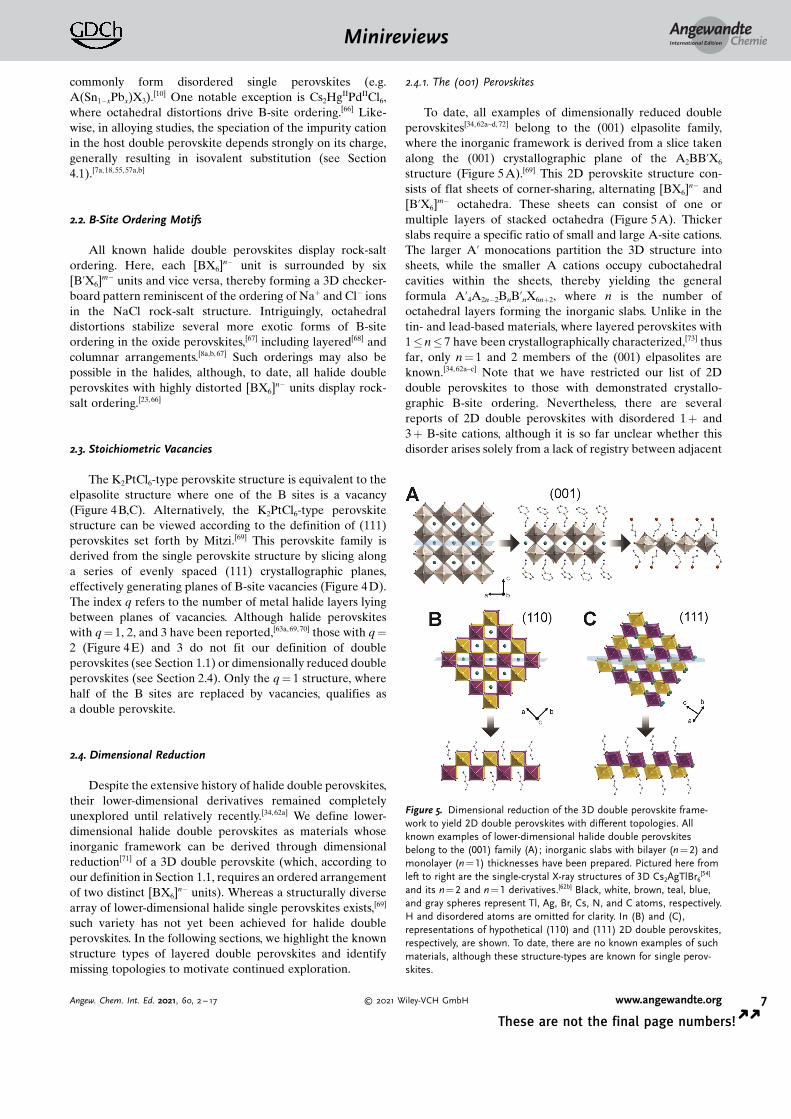
To date, all examples of dimensionally reduced doubleperovskites[34, 62a–d, 72] belong to the (001) elpasolite family,where the inorganic framework is derived from a slice takenalong the (001) crystallographic plane of the A2BB’X6
structure (Figure 5 A).[69] This 2D perovskite structure con-sists of flat sheets of corner-sharing, alternating [BX6]
n� and[B’X6]
m� octahedra. These sheets can consist of one ormultiple layers of stacked octahedra (Figure 5A). Thickerslabs require a specific ratio of small and large A-site cations.The larger A’ monocations partition the 3D structure intosheets, while the smaller A cations occupy cuboctahedralcavities within the sheets, thereby yielding the generalformula A’4A2n�2BnB’nX6n+2, where n is the number ofoctahedral layers forming the inorganic slabs. Unlike in thetin- and lead-based materials, where layered perovskites with1� n� 7 have been crystallographically characterized,[73] thusfar, only n = 1 and 2 members of the (001) elpasolites areknown.[34,62a–c] Note that we have restricted our list of 2Ddouble perovskites to those with demonstrated crystallo-graphic B-site ordering. Nevertheless, there are severalreports of 2D double perovskites with disordered 1 + and3 + B-site cations, although it is so far unclear whether thisdisorder arises solely from a lack of registry between adjacent
Figure 5. Dimensional reduction of the 3D double perovskite frame-work to yield 2D double perovskites with different topologies. Allknown examples of lower-dimensional halide double perovskitesbelong to the (001) family (A); inorganic slabs with bilayer (n = 2) andmonolayer (n = 1) thicknesses have been prepared. Pictured here fromleft to right are the single-crystal X-ray structures of 3D Cs2AgTlBr6
[54]
and its n= 2 and n = 1 derivatives.[62b] Black, white, brown, teal, blue,and gray spheres represent Tl, Ag, Br, Cs, N, and C atoms, respectively.H and disordered atoms are omitted for clarity. In (B) and (C),representations of hypothetical (110) and (111) 2D double perovskites,respectively, are shown. To date, there are no known examples of suchmaterials, although these structure-types are known for single perov-skites.
AngewandteChemieMinireviews
7Angew. Chem. Int. Ed. 2021, 60, 2 – 17 � 2021 Wiley-VCH GmbH www.angewandte.org
These are not the final page numbers! � �
perovskite sheets or also from a random distribution of the B-site cations within the same sheet.[62e, 74]
2.4.2. The (110) and (111) Perovskites
Lower-dimensional perovskites with inorganic slabs de-rived from the (110) and (111) crystallographic planes of the3D single perovskite structure are well-known.[69] However, todate, there are no examples of (110) double perovskites.Likewise, while the K2PtCl6-type perovskites belong to the(111) family (see Section 2.3, Figure 4D),[69] these materialsdo not qualify as dimensionally reduced double perovskitesbecause we consider relatively undistorted vacancies tobe distinct [BX6]
6� motifs that should be included whenevaluating the structural connectivity. The perovskiteCs4CuIISbIII
2Cl12, which consists of (111) layers of threechemically different ordered [BX6]
n� motifs ([CuCl6]4�,
[SbCl6]3�, and [&Cl6]
6�)[70] also does not fit our definition ofa dimensionally reduced double perovskite. The unreported(110) and (111) families of dimensionally reduced halidedouble perovskites (Figure 5B,C) present intriguing synthetictargets, which may exhibit properties quite different fromtheir (001) counterparts, as shown for the lead-halide singleperovskites.[75]
2.5. Structural Distortions
Structural distortions of the perovskite framework arewell-known to have important consequences for a material�soptical and electronic properties.[76] In the following sections,we discuss structural distortions found in halide doubleperovskites.
2.5.1. Structural Distortions of Elpasolites
Theoretically, double perovskites can undergo manydifferent tilting distortions, as studied in detail by Woodwardand co-workers.[77] However, nearly all elpasolites with X =
Cl� , Br� , I� belong to the cubic space group Fm3̄m at roomtemperature and, thus, exhibit perfect octahedral coordina-tion of the B-site cations and no octahedral rotation. Notableexceptions include tetragonal Cs2AuIAuIIIX6 (X = Cl� , Br� ,I�)[23] and Cs2HgPdCl6
[66] (in which the B and B’ centers adoptlinear and square-planar geometries, respectively), rhombo-hedral (MA)2KBiCl6 (with room-temperature B-X-B’ bondangles differing from 1808),[78] and several halide cryolites (asubset of the elpasolites with the general formula AI
2AIBIIIX6)
including Na2NaGdBr6.[79] Indeed, both octahedral distortions
and tilting are observed in the halide cryolite family, whichconsists mostly of fluorides.[80]
2.5.2. Octahedral Rotations in K2PtCl6-Type Perovskites
The B-site vacancy in K2PtCl6-type perovskites decreasesthe rigidity of the 3D framework, enabling greater rotationalfreedom of the [BX6]
2� octahedra and a larger diversity of A-site cations. Undistorted octahedral coordination of the B4+
cation is maintained in lower-symmetry K2PtCl6-type perov-
skite structures, where either oversized[81] or undersized A-site cations (see list compiled by Brown[42]) induce octahedraltilting. We consider these non-cubic materials to be doubleperovskites only if the vacancy coordination resembles anoctahedron (see Section 1.1). This definition is subjective; weexpect that future experimental work will elucidate themaximum possible degree of distortion at the vacancies thatstill maintains the properties of a double perovskite. Besidesthese static distortions, anharmonic lattice dynamics, similarto those studied in single perovskites,[82] are widely reported inK2PtCl6-type perovskites[83] and are discussed elsewhere inmore detail.[61b] As one example, the coupling of cesiumdisplacements with octahedral rotations breaks the harmonicbehavior of vibrations in both CsSnIII3
[82a] and Cs2SnIVI6,[84]
thus illustrating the generality of structural phenomena insingle and double perovskites.
2.5.3. Distortions in 2D Double Perovskites
All 2D halide double perovskites reported to date exhibitsignificant local structural distortions,[34, 62a–d, 72] likely enabledby the enhanced structural flexibility afforded by the 2Dframework relative to the 3D framework. The strict geo-metrical constraints imposed by the 3D perovskite structureare much less important in 2D structures, enabling the [BX6]
n�
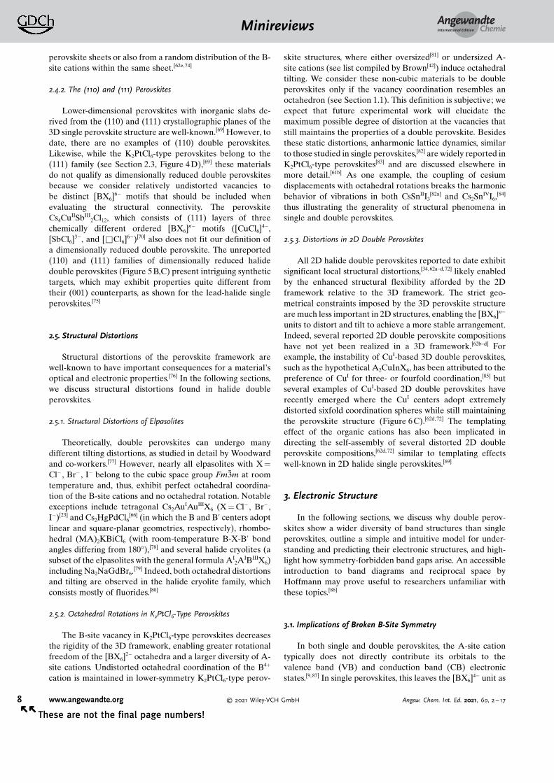
units to distort and tilt to achieve a more stable arrangement.Indeed, several reported 2D double perovskite compositionshave not yet been realized in a 3D framework.[62b–d] Forexample, the instability of CuI-based 3D double perovskites,such as the hypothetical A2CuInX6, has been attributed to thepreference of CuI for three- or fourfold coordination,[85] butseveral examples of CuI-based 2D double perovskites haverecently emerged where the CuI centers adopt extremelydistorted sixfold coordination spheres while still maintainingthe perovskite structure (Figure 6C).[62d, 72] The templatingeffect of the organic cations has also been implicated indirecting the self-assembly of several distorted 2D doubleperovskite compositions,[62d, 72] similar to templating effectswell-known in 2D halide single perovskites.[69]
3. Electronic Structure
In the following sections, we discuss why double perov-skites show a wider diversity of band structures than singleperovskites, outline a simple and intuitive model for under-standing and predicting their electronic structures, and high-light how symmetry-forbidden band gaps arise. An accessibleintroduction to band diagrams and reciprocal space byHoffmann may prove useful to researchers unfamiliar withthese topics.[86]
3.1. Implications of Broken B-Site Symmetry
In both single and double perovskites, the A-site cationtypically does not directly contribute its orbitals to thevalence band (VB) and conduction band (CB) electronicstates.[9,87] In single perovskites, this leaves the [BX6]
4� unit as
AngewandteChemieMinireviews
8 www.angewandte.org � 2021 Wiley-VCH GmbH Angew. Chem. Int. Ed. 2021, 60, 2 – 17� �
These are not the final page numbers!
the fundamental building block of the material�s electronicstates,[87] whereas the electronic structure in double perov-skites is constructed from the combination of [BX6]
n� and[B’X6]
m� units.[9] This broken B-site symmetry leads tosignificantly more possible electronic structures for doubleperovskites compared to single perovskites.
In addition to creating a larger variety of electronicstructures, the broken B-site symmetry can also fundamen-tally change the nature of the band-edge optical transition indouble perovskites. In the well-studied lead-halide perov-skites, the band gap can be viewed as a ligand-to-metalcharge-transfer (LMCT) transition between halide p-orbital-dominated states in the VB (albeit with Pb s-orbital charac-ter) to Pb p-orbital-dominated states in the CB.[88] SimilarLMCT band gaps occur in some double perovskites, partic-ularly the K2PtCl6-type perovskites.[7b, 9,61a,c,89] However, formany elpasolites, the band-edge transition has significantmetal-to-metal charge-transfer (MMCT) character.[9] In theearly literature, the jet black color and polarization-depen-dent absorption spectra of mixed-valence gold double per-ovskites were attributed to a AuI!AuIII intervalence chargetransfer (IVCT).[28c] More recently, our work on the doubleperovskites Cs2AgTlX6 (X = Cl� , Br�) showed that the VBstates have a large degree of Ag+ d character and the CBstates have significant Tl3+ s character. As a consequence ofthe relatively small difference in energy between the [AgX6]
5�
HOMO and [TlX6]3� LUMO, the MMCT nature of the band
gap results in an abnormally small band gap of 0.95 eV forX = Br� (2.0 eV for X = Cl�).[54] Tuning this MMCT transitionin elpasolites through proper selection of B/B’ combinationsoffers a powerful way to control the band gap.[54]
3.2. Predictions of the Electronic Structure from OrbitalSymmetry
Seeking a chemically intuitive interpretation of doubleperovskite band structures, our group developed a qualitativelinear combination of atomic orbitals (LCAO) framework.[9]
Using this approach, a qualitatively accurate band structure ofnearly every known halide double perovskite can be deter-mined by considering only the bonding and antibondinginteractions between nearest neighbors (B-X interactions)and next-nearest neighbors (interactions between halides atright angles from one another within the same octahedron).The positions of the valence band maximum (VBM) andconduction band minimum (CBM) depend strongly on thematch or mismatch in symmetry between the B and B’frontier atomic orbitals. Isoelectronic combinations of B andB’ cations give rise to direct band gaps, whereas other B andB’ combinations can produce either indirect or direct bandgaps. Overall, this LCAO model allows prediction of theVBM and CBM of a double perovskite, often from itschemical formula alone (Table 1).
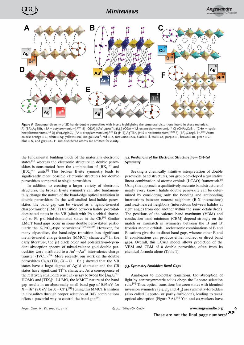
3.3. Symmetry-Forbidden Band Gaps
Analogous to molecular transitions, the absorption oflight by centrosymmetric solids obeys the Laporte selectionrule.[90] Thus, optical transitions between states with identicalinversion symmetry (e.g. Eg and A1g) are symmetry-forbidden(also called Laporte- or parity-forbidden), leading to weakoptical absorption (Figure 7A).[90] Yan and co-workers have
Figure 6. Structural diversity of 2D halide double perovskites with insets highlighting the structural distortions found in these materials.A) (BA)4AgBiBr8 (BA= butylammonium),[62a] B) (ODA)2[(AuII2)(AuIIII4)(I3)2] (ODA = 1,8-octanediammonium),[34] C) (CHA)4CuBiI8 (CHA = cyclo-heptylammonium),[72] D) (PA)4AgInCl8 (PA =propylammonium),[62c] E) (HIS)2AgTlBr8 (HIS = histammonium),[62b] F) (BA)2CsAgBiBr7.
[62a] Atomcolors: orange= Bi, white =Ag, yellow=AuI, indigo= AuIII, red = In, turquoise= Cu, black = Tl, teal = Cs, purple= I, brown = Br, green = Cl,blue = N, and gray= C. H and disordered atoms are omitted for clarity.
AngewandteChemieMinireviews
9Angew. Chem. Int. Ed. 2021, 60, 2 – 17 � 2021 Wiley-VCH GmbH www.angewandte.org
These are not the final page numbers! � �
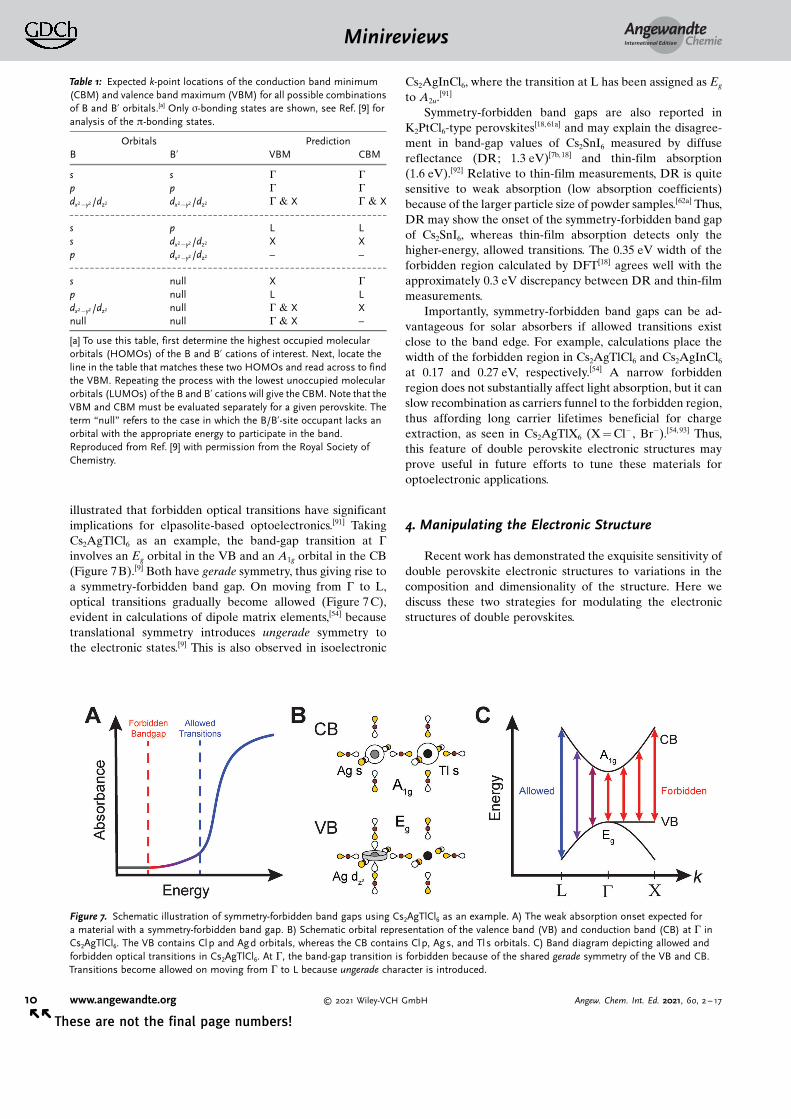
illustrated that forbidden optical transitions have significantimplications for elpasolite-based optoelectronics.[91] TakingCs2AgTlCl6 as an example, the band-gap transition at G
involves an Eg orbital in the VB and an A1g orbital in the CB(Figure 7B).[9] Both have gerade symmetry, thus giving rise toa symmetry-forbidden band gap. On moving from G to L,optical transitions gradually become allowed (Figure 7C),evident in calculations of dipole matrix elements,[54] becausetranslational symmetry introduces ungerade symmetry tothe electronic states.[9] This is also observed in isoelectronic
Cs2AgInCl6, where the transition at L has been assigned as Eg
to A2u.[91]
Symmetry-forbidden band gaps are also reported inK2PtCl6-type perovskites[18, 61a] and may explain the disagree-ment in band-gap values of Cs2SnI6 measured by diffusereflectance (DR; 1.3 eV)[7b,18] and thin-film absorption(1.6 eV).[92] Relative to thin-film measurements, DR is quitesensitive to weak absorption (low absorption coefficients)because of the larger particle size of powder samples.[62a] Thus,DR may show the onset of the symmetry-forbidden band gapof Cs2SnI6, whereas thin-film absorption detects only thehigher-energy, allowed transitions. The 0.35 eV width of theforbidden region calculated by DFT[18] agrees well with theapproximately 0.3 eV discrepancy between DR and thin-filmmeasurements.
Importantly, symmetry-forbidden band gaps can be ad-vantageous for solar absorbers if allowed transitions existclose to the band edge. For example, calculations place thewidth of the forbidden region in Cs2AgTlCl6 and Cs2AgInCl6
at 0.17 and 0.27 eV, respectively.[54] A narrow forbiddenregion does not substantially affect light absorption, but it canslow recombination as carriers funnel to the forbidden region,thus affording long carrier lifetimes beneficial for chargeextraction, as seen in Cs2AgTlX6 (X = Cl� , Br�).[54, 93] Thus,this feature of double perovskite electronic structures mayprove useful in future efforts to tune these materials foroptoelectronic applications.
4. Manipulating the Electronic Structure
Recent work has demonstrated the exquisite sensitivity ofdouble perovskite electronic structures to variations in thecomposition and dimensionality of the structure. Here wediscuss these two strategies for modulating the electronicstructures of double perovskites.
Figure 7. Schematic illustration of symmetry-forbidden band gaps using Cs2AgTlCl6 as an example. A) The weak absorption onset expected fora material with a symmetry-forbidden band gap. B) Schematic orbital representation of the valence band (VB) and conduction band (CB) at G inCs2AgTlCl6. The VB contains Clp and Agd orbitals, whereas the CB contains Clp, Ags, and Tls orbitals. C) Band diagram depicting allowed andforbidden optical transitions in Cs2AgTlCl6. At G, the band-gap transition is forbidden because of the shared gerade symmetry of the VB and CB.Transitions become allowed on moving from G to L because ungerade character is introduced.
Table 1: Expected k-point locations of the conduction band minimum(CBM) and valence band maximum (VBM) for all possible combinationsof B and B’ orbitals.[a] Only s-bonding states are shown, see Ref. [9] foranalysis of the p-bonding states.
Orbitals PredictionB B’ VBM CBM
s s G G
p p G G
dx2�y2 /dz2 dx2�y2 /dz2 G & X G & X
s p L Ls dx2�y2 /dz2 X Xp dx2�y2 /dz2 – –
s null X G
p null L Ldx2�y2 /dz2 null G & X Xnull null G & X –
[a] To use this table, first determine the highest occupied molecularorbitals (HOMOs) of the B and B’ cations of interest. Next, locate theline in the table that matches these two HOMOs and read across to findthe VBM. Repeating the process with the lowest unoccupied molecularorbitals (LUMOs) of the B and B’ cations will give the CBM. Note that theVBM and CBM must be evaluated separately for a given perovskite. Theterm “null” refers to the case in which the B/B’-site occupant lacks anorbital with the appropriate energy to participate in the band.Reproduced from Ref. [9] with permission from the Royal Society ofChemistry.
AngewandteChemieMinireviews
10 www.angewandte.org � 2021 Wiley-VCH GmbH Angew. Chem. Int. Ed. 2021, 60, 2 – 17� �
These are not the final page numbers!
4.1. Alloying
Double perovskites are very tolerant hosts forimpurity alloying, and the effects of substoichiometric sub-stitution of a range of different B-site cations have beenexplored.[7a,18, 27a, 55, 57,94] In isovalent alloys, in which theimpurity cation replaces a cation of the same charge, stablesolid solutions generally form across most or all of thecomposition range. In aliovalent alloys, introducing dopantsoften generates cation vacancies (such as Ag+ vacancies[57c])because of the charge mismatch between the impurity cationand the cation it replaces. This limits the range of achievablecompositions to low dopant concentrations (typically< 1 atom%).[57c,94a] However, substitution of Sn4+ cations inCs2SnCl6 by equal amounts of Sb3+ and Sb5+ demonstratesthat, in some cases, formation of charge-compensatingvacancies can be avoided in aliovalent alloys, thus affordinggreater compositional flexibility.[47] Nevertheless, even atimpurity concentrations as low as 1 atom%, both iso- andaliovalent alloying can dramatically modify the size andsymmetry of the host material�s band gap.[57b, c]
Isoelectronic alloys involve substitution of a cation in thehost structure by an impurity cation that has the sameelectronic configuration. Thus, a change in the symmetry ofthe band gap is not expected (see Section 3.2), only a modi-fication of its size. For example, in Cs2Ag(Bi1�xSbx)Br6 theband gap drops gradually with increasing Sb3+ substitution,but remains indirect throughout.[57a] This decrease in the bandgap is almost entirely caused by an increase in the energy ofthe s-orbital-based VBM and can be understood by notingthat the Sb3+ 5s orbital is higher in energy than the Bi3+ 6sorbital due to relativistic effects.
In non-isoelectronic alloys, the impurity does not have thesame electronic configuration as the cation it replaces, so boththe symmetry and size of the band gap should change atsufficiently high levels of alloying. In the two closely relatedalloys Cs2Ag(Bi1�xInx)Br6
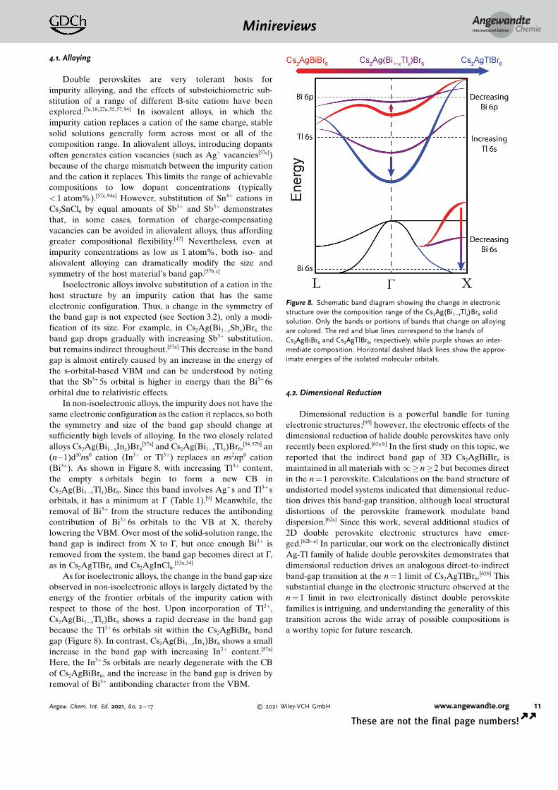
[57a] and Cs2Ag(Bi1�xTlx)Br6,[54, 57b] an
(n�1)d10ns0 cation (In3+ or Tl3+) replaces an ns2np0 cation(Bi3+). As shown in Figure 8, with increasing Tl3+ content,the empty s orbitals begin to form a new CB inCs2Ag(Bi1�xTlx)Br6. Since this band involves Ag+ s and Tl3+ sorbitals, it has a minimum at G (Table 1).[9] Meanwhile, theremoval of Bi3+ from the structure reduces the antibondingcontribution of Bi3+ 6s orbitals to the VB at X, therebylowering the VBM. Over most of the solid-solution range, theband gap is indirect from X to G, but once enough Bi3+ isremoved from the system, the band gap becomes direct at G,as in Cs2AgTlBr6 and Cs2AgInCl6.
[53a, 54]
As for isoelectronic alloys, the change in the band gap sizeobserved in non-isoelectronic alloys is largely dictated by theenergy of the frontier orbitals of the impurity cation withrespect to those of the host. Upon incorporation of Tl3+,Cs2Ag(Bi1�xTlx)Br6 shows a rapid decrease in the band gapbecause the Tl3+ 6s orbitals sit within the Cs2AgBiBr6 bandgap (Figure 8). In contrast, Cs2Ag(Bi1�xInx)Br6 shows a smallincrease in the band gap with increasing In3+ content.[57a]
Here, the In3+ 5s orbitals are nearly degenerate with the CBof Cs2AgBiBr6, and the increase in the band gap is driven byremoval of Bi3+ antibonding character from the VBM.
4.2. Dimensional Reduction
Dimensional reduction is a powerful handle for tuningelectronic structures;[95] however, the electronic effects of thedimensional reduction of halide double perovskites have onlyrecently been explored.[62a,b] In the first study on this topic, wereported that the indirect band gap of 3D Cs2AgBiBr6 ismaintained in all materials with1� n� 2 but becomes directin the n = 1 perovskite. Calculations on the band structure ofundistorted model systems indicated that dimensional reduc-tion drives this band-gap transition, although local structuraldistortions of the perovskite framework modulate banddispersion.[62a] Since this work, several additional studies of2D double perovskite electronic structures have emer-ged.[62b–e] In particular, our work on the electronically distinctAg-Tl family of halide double perovskites demonstrates thatdimensional reduction drives an analogous direct-to-indirectband-gap transition at the n = 1 limit of Cs2AgTlBr6.
[62b] Thissubstantial change in the electronic structure observed at then = 1 limit in two electronically distinct double perovskitefamilies is intriguing, and understanding the generality of thistransition across the wide array of possible compositions isa worthy topic for future research.
Figure 8. Schematic band diagram showing the change in electronicstructure over the composition range of the Cs2Ag(Bi1�xTlx)Br6 solidsolution. Only the bands or portions of bands that change on alloyingare colored. The red and blue lines correspond to the bands ofCs2AgBiBr6 and Cs2AgTlBr6, respectively, while purple shows an inter-mediate composition. Horizontal dashed black lines show the approx-imate energies of the isolated molecular orbitals.
AngewandteChemieMinireviews
11Angew. Chem. Int. Ed. 2021, 60, 2 – 17 � 2021 Wiley-VCH GmbH www.angewandte.org
These are not the final page numbers! � �
5. Outlook
Modern research on halide double perovskites bringstogether two materials families, elpasolites and K2PtCl6-typeperovskites, which were historically independent. The uni-fication of these two structure-types was enabled by obser-vations of their structural,[16,96] optical,[18, 54,91] and electro-nic[9, 54,61b] similarities and helped advance understanding ofboth families, as insight gained into one could inform researchon the other. As we move forward, seeking to furtherunderstand, develop, and utilize halide double perovskites,we should learn from this historical precedent and continue tosearch for parallels between halide double perovskites andother well-studied materials families (Figure 9). Thus, to closethis Minireview, we highlight similarities between halidedouble perovskites and other important classes of materials.We end with a very brief discussion of potential applicationsof halide double perovskites.
5.1. The Prussian Blue Analogues (PBAs)
The MMCT nature of the band-gap transition of manyelpasolites affords a direct means of manipulating the gap byselecting [BX6]
n� and [B’X6]m�molecular hexahalides with the
desired HOMO and LUMO energy levels (see Section 3.1).However, the exploitation of MMCT transitions in theperovskite field[54] is long predated by studies of suchtransitions in the PBAs, a closely related materials family.Prussian Blue (PB; Fe4
III[FeII(CN)6]3·14H2O) can be consid-ered a double perovskite in which cyanides (pseudohalides)replace the halides, all A-sites are vacant, and 25% of the[FeII(CN)6]
4� units are missing. PB has a rich history as one ofthe earliest synthetic blue pigments and its intense color arises
from an FeII!FeIII MMCT. It was first made by accident bythe German pigment maker Heinrich Diesbach while at-tempting to make a violet pigment from a mixture containingFeIII
2(SO4)3 and potash. However, unbeknownst to him, hispotash had previously been used by the alchemist JohannDippel to prepare a concoction involving animal blood. Asa result, it was contaminated with FeII and cyanide, thusproviding the necessary ingredients to make PB.[97] Since itssynthesis, PB has been used in historical works of art such asthe “Great Wave off Kanagawa” (ca. 1830). Revisiting thevast literature on tuning the MMCT transition of PBAs[28c,98]
may teach us how to adapt halide double perovskites toabsorb sunlight in solar cells. Similar to the careful studies on[M(CN)6]
n� molecules,[99] studying the energy levels of[BX6]
n� molecules that form the building blocks of elpasolitesshould allow us to predict and manipulate the magnitude oftheir band gaps.
A similar analogy exists between layered double perov-skites and Hofmann clathrates such as NiII(CN)4·NiII(NH3)2,the layered counterparts of PBAs.[100] However, in contrast tothe organoammonium cations in layered halide perovskites,neutral amines that coordinate to the metal cations comprisethe organic layers in Hofmann clathrates.
5.2. The Transition-Metal Dichalcogenides (TMDCs)
Recent work has uncovered dramatic changes in band-gapsymmetry (direct/indirect) upon dimensional reduction of the3D halide double perovskite structure to the 2D monolayerstructure (see Section 4.2).[62a,b] These findings are reminis-cent of the well-known indirect-to-direct band gap transitionin TMDCs, such as MoS2, which occurs when the bulkmaterial is exfoliated to a single monolayer.[101] The thoroughunderstanding of this band-gap transition in the TMDCs laidthe groundwork for unique applications of these materials.[102]
Thus, as researchers continue to expand the field of halidedouble perovskites, we should seek a similar understanding ofthe orbital basis for changes in band-gap symmetry withdimensionality.
5.3. Molecular BX6 Complexes
The electronic properties of K2PtCl6-type perovskites arelargely determined by the [BX6]
2� complex, thereby offeringa platform to study the behavior of metal-halide octahedra inthe solid state, in parallel with many prior studies onmolecules in solution. For example, the splitting of the bandcorresponding to the s!p transition in [TeX6]
2� (X = Cl� ,Br�) molecules evidenced lower symmetry (Oh!C2v) in theirphotoexcited states.[103] Similar distorted excited states havebeen invoked to explain the Stokes-shifted photolumines-cence of halide perovskites.[63b] In addition, similar to theLMCT nature of the band gap in K2PtCl6-type perovskites,the primary photoreduction pathway for PtCl6
2� molecules isalso an inner-sphere LMCT.[104] The solid-state packinginteractions in double perovskites also stabilize differentgeometries. For example, the intriguing high-pressure redox
Figure 9. Comparison of halide perovskites (A,[54] B,[62a] and C[106]) withthe well-known Prussian Blue (D), transition-metal dichalcogenide (E),and oxide perovskite (F) families, which provide historical precedent.Atom colors: teal = Cs, white= Ag, black =Tl, light orange= Bi, lightpurple= Na, dark purple=Mo, light blue = La, gold= Cu, darkgreen = Sn, crimson= FeII, orange=FeIII, brown= Br, green = Cl,blue = N, red = O, yellow=S, and gray =C. H and disordered atomsare omitted for clarity.
AngewandteChemieMinireviews
12 www.angewandte.org � 2021 Wiley-VCH GmbH Angew. Chem. Int. Ed. 2021, 60, 2 – 17� �
These are not the final page numbers!
transformation of Cs2PdIII4·I2 to Cs2PdIVI6 demonstratesinterchangeable coordination from square-planar [PdIII4]
2�
to octahedral [PdIVI6]2�.[105] Although interoctahedral inter-
actions in K2PtCl6-type perovskites are historically disregard-ed,[103] recent work illustrates that interactions across thevacancies, particularly in iodide perovskites, generate dis-perse CBs.[18] Moving forward, it is worth developing a morenuanced understanding of interoctahedral interactions inK2PtCl6-type perovskites, which exist on the conceptualborder between molecular salts with localized orbitals andsemiconductors with delocalized bands.
5.4. Other Perovskites
While seemingly trivial, we must not lose sight of the factthat both oxide double perovskites and halide single per-ovskites boast structure types not yet observed in halidedouble perovskites. As illustrated by Cs2NaBiCl6 (Fig-ure 9C),[106] halide double perovskites exhibit rock salt B-siteordering. Oxide double perovskites display B-site orderingsunknown in the halides (see Section 2.2),[8a, b, 67] and diversestructural topologies exist for lower-dimensional halide singleperovskites that remain unknown in the double perovskites(see Section 2.4).[63a] Such materials represent worthy syn-thetic targets that may afford novel properties.
5.5. Applications
Although this Minireview is focused on fundamentalstudies, we note that 3D double perovskites have previouslybeen considered for applications in lasing,[27a,b] scintilla-tion,[27c] and upconversion.[27d, 48] More recently, 3D doubleperovskites have been considered as components of electro-luminescent devices,[7a] X-ray detectors,[7d, 107] and solar cells aseither absorbers[7c] or hole-transport layers.[7b] The perfor-mance of double perovskites in some of these newerapplications is still evolving because efficiencies dependheavily on film morphology and defects, which will likely bebetter understood and controlled through future studies. Forexample, as a consequence of its indirect band gap,Cs2AgBiBr6 films used as solar absorbers must be micro-meters thick to adequately absorb sunlight[52a] (similar to Siabsorbers), and preparing thick, high-quality films of thesequaternary compounds remains a challenge. Recent studiesalso show that long carrier diffusion lengths (ca. 11 mm) maybe realized in Cs2AgBiBr6 if surface trap states are passivat-ed,[93] thus motivating studies on the defect chemistry ofdouble perovskites.
The stunning diversity of chemical compositions andelectronic structures afforded by the two distinct B sites ofdouble perovskites brings with it a mighty challenge: can wepredict which B-site combinations will provide the desiredproperties? Despite their long history, foundationalstudies on halide double perovskites are still needed forus to shrewdly place our bets and win, as the stakes aredoubled.
Acknowledgements
This work was supported by the Department of Energy,Office of Basic Energy Sciences, Division of MaterialsSciences and Engineering, under contract DE-AC02-76SF00515. N.R.W. is supported by a Stanford Interdiscipli-nary Graduate Fellowship. B.A.C. was supported by an NSFgraduate fellowship (DGE-114747) and the Evelyn McBainaward from Stanford Chemistry. A.H.S. was supported bya Stanford Graduate Fellowship and the Veatch award fromStanford Chemistry.
Conflict of interest
The authors declare no conflict of interest.
[1] a) W. Cross, W. F. Hillebrand, Am. J. Sci. 1883, s3-26, 271;b) H. L. Wells, Am. J. Sci. 1893, s3-45, 121.
[2] a) D. Weber, Z. Naturforsch. B 1978, 33, 1443; b) A. Kojima, K.Teshima, Y. Shirai, T. Miyasaka, J. Am. Chem. Soc. 2009, 131,6050.
[3] a) D. P. McMeekin, G. Sadoughi, W. Rehman, G. E. Eperon, M.Saliba, M. T. Hçrantner, A. Haghighirad, N. Sakai, L. Korte, B.Rech, M. B. Johnston, L. M. Herz, H. J. Snaith, Science 2016,351, 151; b) M. Saliba, T. Matsui, J.-Y. Seo, K. Domanski, J.-P.Correa-Baena, M. K. Nazeeruddin, S. M. Zakeeruddin, W.Tress, A. Abate, A. Hagfeldt, M. Gr�tzel, Energy Environ.Sci. 2016, 9, 1989; c) J. Xu, C. C. Boyd, Z. J. Yu, A. F.Palmstrom, D. J. Witter, B. W. Larson, R. M. France, J. Werner,S. P. Harvey, E. J. Wolf, W. Weigand, S. Manzoor, M. F. A. M.van Hest, J. J. Berry, J. M. Luther, Z. C. Holman, M. D.McGehee, Science 2020, 367, 1097.
[4] a) A. H. Slavney, R. W. Smaha, I. C. Smith, A. Jaffe, D.Umeyama, H. I. Karunadasa, Inorg. Chem. 2017, 56, 46;b) A. D. Jodlowski, D. Rodr�guez-Padr�n, R. Luque, G. de Mi-guel, Adv. Energy Mater. 2018, 8, 1703120.
[5] a) F. Igbari, Z.-K. Wang, L.-S. Liao, Adv. Energy Mater. 2019, 9,1803150; b) F. Giustino, H. J. Snaith, ACS Energy Lett. 2016, 1,1233.
[6] a) S. E. Creutz, E. N. Crites, M. C. De Siena, D. R. Gamelin,Nano Lett. 2018, 18, 1118; b) F. Locardi, M. Cirignano, D.Baranov, Z. Dang, M. Prato, F. Drago, M. Ferretti, V. Pinchetti,M. Fanciulli, S. Brovelli, L. De Trizio, L. Manna, J. Am. Chem.Soc. 2018, 140, 12989; c) B. Yang, X. Mao, F. Hong, W. Meng, Y.Tang, X. Xia, S. Yang, W. Deng, K. Han, J. Am. Chem. Soc.2018, 140, 17001.
[7] a) J. Luo, X. Wang, S. Li, J. Liu, Y. Guo, G. Niu, L. Yao, Y. Fu, L.Gao, Q. Dong, C. Zhao, M. Leng, F. Ma, W. Liang, L. Wang, S.Jin, J. Han, L. Zhang, J. Etheridge, J. Wang, Y. Yan, E. H.Sargent, J. Tang, Nature 2018, 563, 541; b) B. Lee, C. C.Stoumpos, N. Zhou, F. Hao, C. Malliakas, C.-Y. Yeh, T. J.Marks, M. G. Kanatzidis, R. P. H. Chang, J. Am. Chem. Soc.2014, 136, 15379; c) E. Greul, M. L. Petrus, A. Binek, P.Docampo, T. Bein, J. Mater. Chem. A 2017, 5, 19972; d) W. Pan,H. Wu, J. Luo, Z. Deng, C. Ge, C. Chen, X. Jiang, W.-J. Yin, G.Niu, L. Zhu, L. Yin, Y. Zhou, Q. Xie, X. Ke, M. Sui, J. Tang, Nat.Photonics 2017, 11, 726.
[8] a) M. T. Anderson, K. B. Greenwood, G. A. Taylor, K. R.Poeppelmeier, Prog. Solid State Chem. 1993, 22, 197; b) S.Vasala, M. Karppinen, Prog. Solid State Chem. 2015, 43, 1; c) N.Mercier, Angew. Chem. Int. Ed. 2019, 58, 17912; Angew. Chem.2019, 131, 18078; d) B. Vargas, G. Rodr�guez-L�pez, D. Solis-Ibarra, ACS Energy Lett. 2020, 5, 3591.
AngewandteChemieMinireviews
13Angew. Chem. Int. Ed. 2021, 60, 2 – 17 � 2021 Wiley-VCH GmbH www.angewandte.org
These are not the final page numbers! � �
[9] A. H. Slavney, B. A. Connor, L. Leppert, H. I. Karunadasa,Chem. Sci. 2019, 10, 11041.
[10] a) J. D. Donaldson, D. Laughlin, S. D. Ross, J. Silver, J. Chem.Soc. Dalton Trans. 1973, 1985; b) J. Barrett, J. D. Donaldson, J.Silver, N. P. Y. Siew, J. Chem. Soc. Dalton Trans. 1977, 906.
[11] a) C. C. Stoumpos, C. D. Malliakas, M. G. Kanatzidis, Inorg.Chem. 2013, 52, 9019; b) G. E. Eperon, T. Leijtens, K. A. Bush,R. Prasanna, T. Green, J. T.-W. Wang, D. P. McMeekin, G.Volonakis, R. L. Milot, R. May, A. Palmstrom, D. J. Slotcavage,R. A. Belisle, J. B. Patel, E. S. Parrott, R. J. Sutton, W. Ma, F.Moghadam, B. Conings, A. Babayigit, H.-G. Boyen, S. Bent, F.Giustino, L. M. Herz, M. B. Johnston, M. D. McGehee, H. J.Snaith, Science 2016, 354, 861; c) C. Wang, Z. Song, C. Li, D.Zhao, Y. Yan, Adv. Funct. Mater. 2019, 29, 1808801.
[12] a) G. Gou, N. Charles, J. Shi, J. M. Rondinelli, Inorg. Chem.2017, 56, 11854; b) A. Aimi, D. Mori, K.-i. Hiraki, T. Takahashi,Y. J. Shan, Y. Shirako, J. Zhou, Y. Inaguma, Chem. Mater. 2014,26, 2601.
[13] M. Ducau, K. S. Suh, J. Senegas, J. Darriet, Mater. Res. Bull.1992, 27, 1115.
[14] W. Cross, W. F. Hillebrand, U.S. Geol. Surv. Bull. 1885, 20, 1.[15] H. L. Wheeler, Am. J. Sci. 1893, s3-45, 267.[16] M. Krupski, Phys. Status Solidi A 1989, 116, 657.[17] D. H. Brown, K. R. Dixon, C. M. Livingston, R. H. Nuttall,
D. W. A. Sharp, J. Chem. Soc. A 1967, 100.[18] A. E. Maughan, A. M. Ganose, M. M. Bordelon, E. M. Miller,
D. O. Scanlon, J. R. Neilson, J. Am. Chem. Soc. 2016, 138, 8453.[19] P. Scherrer, P. Stoll, Z. Anorg. Allg. Chem. 1922, 121, 319.[20] H. L. Wells, Am. J. Sci. 1922, s5-3, 315.[21] G. Menzer, Fortschr. Mineral. Kristallogr. Petrogr. 1932, 17, 61.[22] L. R. Morss, J. Inorg. Nucl. Chem. 1974, 36, 3876.[23] N. Elliott, L. Pauling, J. Am. Chem. Soc. 1938, 60, 1846.[24] a) K. Knox, D. W. Mitchell, J. Inorg. Nucl. Chem. 1961, 21, 253;
b) J.-P. Besse, M. Capestan, C. R. Seances Acad. Sci. Ser. C 1968,266, 551; c) L. R. Morss, M. Siegal, L. Stenger, N. Edelstein,Inorg. Chem. 1970, 9, 1771.
[25] G. Meyer, Prog. Solid State Chem. 1982, 14, 141.[26] a) E. Bucher, H. J. Guggenheim, K. Andres, G. W. Hull, Jr.,
A. S. Cooper, Phys. Rev. B 1974, 10, 2945; b) H.-D. Amberger,G. G. Rosenbauer, R. D. Fischer, J. Phys. Chem. Solids 1977, 38,379.
[27] a) B. F. Aull, H. P. Jenssen, Phys. Rev. B 1986, 34, 6647; b) C.Reber, H. U. G�del, G. Meyer, T. Schleid, C. A. Daul, Inorg.Chem. 1989, 28, 3249; c) C. M. Combes, P. Dorenbos, C. W. E.van Eijk, K. W. Kr�mer, H. U. G�del, J. Lumin. 1999, 82, 299;d) D. R. Gamelin, H. U. G�del, J. Am. Chem. Soc. 1998, 120,12143.
[28] a) S. Yamada, R. Tsuchida, Bull. Chem. Soc. Jpn. 1956, 29, 421;b) G. Brauer, G. Sleater, J. Less-Common Met. 1970, 21, 283;c) M. B. Robin, P. Day in Advances in Inorganic Chemistry andRadiochemistry, Vol. 10 (Eds.: H. J. Emel�us, A. G. Sharpe),Academic Press, New York, 1968, p. 247.
[29] a) R. Keller, J. Fenner, W. B. Holzapfel, Mater. Res. Bull. 1974,9, 1363; b) W. Denner, H. Schulz, H. D’Amour, Acta Crystal-logr. Sect. A 1979, 35, 360; c) J. Stanek, S. S. Hafner, H. Schulz,Phys. Lett. A 1980, 76, 333; d) J. Stanek, J. Chem. Phys. 1982, 76,2315.
[30] R. J. Cava, B. Batlogg, J. J. Krajewski, R. Farrow, L. W.Rupp, Jr., A. E. White, K. Short, W. F. Peck, T. Kometani,Nature 1988, 332, 814.
[31] N. Kojima, H. Kitagawa, T. Ban, F. Amita, M. Nakahara, SolidState Commun. 1990, 73, 743.
[32] a) S. S. Hafner, N. Kojima, J. Stanek, L. Zhang, Phys. Lett. A1994, 192, 385; b) N. Kojima, M. Hasegawa, H. Kitagawa, T.Kikegawa, O. Shimomura, J. Am. Chem. Soc. 1994, 116, 11368.
[33] a) M. Retuerto, T. Emge, J. Hadermann, P. W. Stephens, M. R.Li, Z. P. Yin, M. Croft, A. Ignatov, S. J. Zhang, Z. Yuan, C. Jin,
J. W. Simonson, M. C. Aronson, A. Pan, D. N. Basov, G. Kotliar,M. Greenblatt, Chem. Mater. 2013, 25, 4071; b) M. Retuerto, Z.Yin, T. J. Emge, P. W. Stephens, M.-R. Li, T. Sarkar, M. C.Croft, A. Ignatov, Z. Yuan, S. J. Zhang, C. Jin, R. P. Sena, J.Hadermann, G. Kotliar, M. Greenblatt, Inorg. Chem. 2015, 54,1066.
[34] L. M. Castro-Castro, A. M. Guloy, Angew. Chem. Int. Ed. 2003,42, 2771; Angew. Chem. 2003, 115, 2877.
[35] N. Matsushita, H. Kitagawa, N. Kojima, Acta Crystallogr. Sect.C 1997, 53, 663.
[36] J. J. Berzelius, Ann. Phys. Chem. 1834, 108, 577.[37] a) M. Jacquelain, Ann. Chim. Phys. 1837, 113; b) T. Hiortdahl,
Z. Kristallogr. Cryst. Mater. 1882, 6, 456; c) A. Gutbier, A.Krell, Ber. Dtsch. Chem. Ges. 1905, 38, 2385; d) P. Groth,Chemische Krystallographie, Vol. 1, Wilhelm Engelmann, Leip-zig, 1906, pp. 466 – 535; e) R. L. Datta, J. Am. Chem. Soc. 1913,35, 1185; f) M. Del�pine, Ann. Chim. 1917, 7, 277.
[38] a) R. L. Slagle, PhD thesis, Johns Hopkins University (Balti-more, Maryland, USA), 1894 ; b) A. Rosenheim, H. Aron, Z.Anorg. Allg. Chem. 1904, 39, 170.
[39] a) R. W. G. Wyckoff, E. Posnjak, J. Am. Chem. Soc. 1921, 43,2292; b) R. G. Dickinson, J. Am. Chem. Soc. 1922, 44, 276;c) F. J. Ewing, L. Pauling, Z. Kristallogr. Cryst. Mater. 1928, 68,223; d) P. Stoll, PhD thesis, ETH Z�rich (Z�rich, Switzerland),1926 ; e) W. A. Frederikse, H. J. Verweel, Recl. Trav. Chim.Pays-Bas 1928, 47, 904.
[40] a) G. Engel, Z. Kristallogr. Cryst. Mater. 1935, 90, 341;b) J. A. A. Ketelaar, A. A. Rietdijk, C. H. van Staveren, Recl.Trav. Chim. Pays-Bas 1937, 56, 907; c) J. A. A. Ketelaar, J. F.van Walsem, Recl. Trav. Chim. Pays-Bas 1938, 57, 964; d) W.Werker, Recl. Trav. Chim. Pays-Bas 1939, 58, 257; e) R. W. G.Wyckoff, The Structure of Crystals, 2nd ed., The ChemicalCatalog Company, Inc., New York, 1931, pp. 303 – 306;f) R. W. G. Wyckoff, The Structure of Crystals. Supplement for1930 – 1934 to the Second Edition, Reinhold Publishing Corpo-ration, New York, 1935, pp. 77 – 80.
[41] a) M. G. Brik, I. V. Kityk, J. Phys. Chem. Solids 2011, 72, 1256;b) B. E. Douglas, S.-M. Ho in Structure and Chemistry ofCrystalline Solids, Springer, New York, 2006, pp. 128 – 129.
[42] I. D. Brown, Can. J. Chem. 1964, 42, 2758.[43] V. M. Goldschmidt, Naturwissenschaften 1926, 14, 477.[44] M. Krupski, Phys. Status Solidi A 1983, 78, 751.[45] a) D. Nakamura, Y. Kurita, K. Ito, M. Kubo, J. Am. Chem. Soc.
1960, 82, 5783; b) K. Ito, D. Nakamura, K. Ito, M. Kubo, Inorg.Chem. 1963, 2, 690; c) M. Kubo, D. Nakamura in Advances inInorganic Chemistry and Radiochemistry, Vol. 8 (Eds.: H. J.Emel�us, A. G. Sharpe), Academic Press, New York, 1966,pp. 257 – 282.
[46] a) J. Owen, K. W. H. Stevens, Nature 1953, 171, 836; b) J. H. E.Griffiths, J. Owen, Proc. R. Soc. London Ser. A 1954, 226, 96.
[47] L. Atkinson, P. Day, J. Chem. Soc. A 1969, 2423.[48] D. R. Gamelin, H. U. G�del, Inorg. Chem. 1999, 38, 5154.[49] V. Auger, T. Karantassis, C. R. Hebd. Seances Acad. Sci. 1925,
181, 665.[50] S. J. Clark, J. D. Donaldson, J. A. Harvey, J. Mater. Chem. 1995,
5, 1813.[51] G. Giorgi, K. Yamashita, Chem. Lett. 2015, 44, 826.[52] a) A. H. Slavney, T. Hu, A. M. Lindenberg, H. I. Karunadasa, J.
Am. Chem. Soc. 2016, 138, 2138; b) E. T. McClure, M. R. Ball,W. Windl, P. M. Woodward, Chem. Mater. 2016, 28, 1348; c) G.Volonakis, M. R. Filip, A. A. Haghighirad, N. Sakai, B. Wenger,H. J. Snaith, F. Giustino, J. Phys. Chem. Lett. 2016, 7, 1254.
[53] a) G. Volonakis, A. A. Haghighirad, R. L. Milot, W. H. Sio,M. R. Filip, B. Wenger, M. B. Johnston, L. M. Herz, H. J.Snaith, F. Giustino, J. Phys. Chem. Lett. 2017, 8, 772; b) J. Zhou,Z. Xia, M. S. Molokeev, X. Zhang, D. Peng, Q. Liu, J. Mater.Chem. A 2017, 5, 15031.
AngewandteChemieMinireviews
14 www.angewandte.org � 2021 Wiley-VCH GmbH Angew. Chem. Int. Ed. 2021, 60, 2 – 17� �
These are not the final page numbers!
[54] A. H. Slavney, L. Leppert, A. Saldivar Valdes, D. Bartesaghi,T. J. Savenije, J. B. Neaton, H. I. Karunadasa, Angew. Chem.Int. Ed. 2018, 57, 12765; Angew. Chem. 2018, 130, 12947.
[55] T. T. Tran, J. R. Panella, J. R. Chamorro, J. R. Morey, T. M.McQueen, Mater. Horiz. 2017, 4, 688.
[56] Z. Deng, F. Wei, S. Sun, G. Kieslich, A. K. Cheetham, P. D.Bristowe, J. Mater. Chem. A 2016, 4, 12025.
[57] a) K.-z. Du, W. Meng, X. Wang, Y. Yan, D. B. Mitzi, Angew.Chem. Int. Ed. 2017, 56, 8158; Angew. Chem. 2017, 129, 8270;b) A. H. Slavney, L. Leppert, D. Bartesaghi, A. Gold-Parker,M. F. Toney, T. J. Savenije, J. B. Neaton, H. I. Karunadasa, J.Am. Chem. Soc. 2017, 139, 5015; c) K. P. Lindquist, S. A. Mack,A. H. Slavney, L. Leppert, A. Gold-Parker, J. F. Stebbins, A.Salleo, M. F. Toney, J. B. Neaton, H. I. Karunadasa, Chem. Sci.2019, 10, 10620.
[58] V. Auger, T. Karantassis, C. R. Hebd. Seances Acad. Sci. 1925,180, 1845.
[59] D. H. Brown, K. R. Dixon, D. W. A. Sharp, J. Chem. Soc. A1966, 1244.
[60] D. Sinram, C. Brendel, B. Krebs, Inorg. Chim. Acta 1982, 64,L131.
[61] a) N. Sakai, A. A. Haghighirad, M. R. Filip, P. K. Nayak, S.Nayak, A. Ramadan, Z. Wang, F. Giustino, H. J. Snaith, J. Am.Chem. Soc. 2017, 139, 6030; b) A. E. Maughan, A. M. Ganose,D. O. Scanlon, J. R. Neilson, Chem. Mater. 2019, 31, 1184;c) M.-G. Ju, M. Chen, Y. Zhou, H. F. Garces, J. Dai, L. Ma, N. P.Padture, X. C. Zeng, ACS Energy Lett. 2018, 3, 297.
[62] a) B. A. Connor, L. Leppert, M. D. Smith, J. B. Neaton, H. I.Karunadasa, J. Am. Chem. Soc. 2018, 140, 5235; b) B. A.Connor, R.-I. Biega, L. Leppert, H. I. Karunadasa, Chem. Sci.2020, 11, 7708; c) L. Mao, S. M. L. Teicher, C. C. Stoumpos,R. M. Kennard, R. A. DeCrescent, G. Wu, J. A. Schuller, M. L.Chabinyc, A. K. Cheetham, R. Seshadri, J. Am. Chem. Soc.2019, 141, 19099; d) L.-Y. Bi, Y.-Q. Hu, M.-Q. Li, T.-L. Hu, H.-L. Zhang, X.-T. Yin, W.-X. Que, M. S. Lassoued, Y.-Z. Zheng, J.Mater. Chem. A 2019, 7, 19662; e) M. K. Jana, S. M. Janke, D. J.Dirkes, S. Dovletgeldi, C. Liu, X. Qin, K. Gundogdu, W. You, V.Blum, D. B. Mitzi, J. Am. Chem. Soc. 2019, 141, 7955.
[63] a) B. Saparov, D. B. Mitzi, Chem. Rev. 2016, 116, 4558; b) M. D.Smith, B. A. Connor, H. I. Karunadasa, Chem. Rev. 2019, 119,3104.
[64] J. Yang, P. Zhang, S.-H. Wei, J. Phys. Chem. Lett. 2018, 9, 31.[65] Z. Xiao, W. Meng, J. Wang, Y. Yan, ChemSusChem 2016, 9,
2628.[66] L. Schrçder, H.-L. Keller, Z. Anorg. Allg. Chem. 1991, 603, 69.[67] G. King, P. M. Woodward, J. Mater. Chem. 2010, 20, 5785.[68] a) M. T. Anderson, K. R. Poeppelmeier, Chem. Mater. 1991, 3,
476; b) M. Azuma, S. Kaimori, M. Takano, Chem. Mater. 1998,10, 3124.
[69] D. B. Mitzi, J. Chem. Soc. Dalton Trans. 2001, 1.[70] B. Vargas, E. Ramos, E. P�rez-Guti�rrez, J. C. Alonso, D. Solis-
Ibarra, J. Am. Chem. Soc. 2017, 139, 9116.[71] E. G. Tulsky, J. R. Long, Chem. Mater. 2001, 13, 1149.[72] L.-Y. Bi, T.-L. Hu, M.-Q. Li, B.-K. Ling, M. S. Lassoued, Y.-Q.
Hu, Z. Wu, G. Zhou, Y.-Z. Zheng, J. Mater. Chem. A 2020, 8,7288.
[73] a) S. S. Nagapetyan, Y. I. Dolzhenko, E. R. Arakelova, V. M.Koshkin, Y. T. Struchkov, V. E. Shklover, Zh. Neorg. Khim.1988, 33, 2806; b) J. Calabrese, N. L. Jones, R. L. Harlow, N.Herron, D. L. Thorn, Y. Wang, J. Am. Chem. Soc. 1991, 113,2328; c) D. B. Mitzi, C. A. Feild, W. T. A. Harrison, A. M.Guloy, Nature 1994, 369, 467; d) I. C. Smith, E. T. Hoke, D.Solis-Ibarra, M. D. McGehee, H. I. Karunadasa, Angew. Chem.Int. Ed. 2014, 53, 11232; Angew. Chem. 2014, 126, 11414;e) C. M. M. Soe, G. P. Nagabhushana, R. Shivaramaiah, H.Tsai, W. Nie, J.-C. Blancon, F. Melkonyan, D. H. Cao, B. Traor�,L. Pedesseau, M. Kepenekian, C. Katan, J. Even, T. J. Marks, A.
Navrotsky, A. D. Mohite, C. C. Stoumpos, M. G. Kanatzidis,Proc. Natl. Acad. Sci. USA 2019, 116, 58.
[74] E. T. McClure, A. P. McCormick, P. M. Woodward, Inorg.Chem. 2020, 59, 6010.
[75] a) E. R. Dohner, E. T. Hoke, H. I. Karunadasa, J. Am. Chem.Soc. 2014, 136, 1718; b) E. R. Dohner, A. Jaffe, L. R. Bradshaw,H. I. Karunadasa, J. Am. Chem. Soc. 2014, 136, 13154; c) M. D.Smith, H. I. Karunadasa, Acc. Chem. Res. 2018, 51, 619.
[76] a) R. Prasanna, A. Gold-Parker, T. Leijtens, B. Conings, A.Babayigit, H.-G. Boyen, M. F. Toney, M. D. McGehee, J. Am.Chem. Soc. 2017, 139, 11117; b) M. D. Smith, A. Jaffe, E. R.Dohner, A. M. Lindenberg, H. I. Karunadasa, Chem. Sci. 2017,8, 4497.
[77] C. J. Howard, B. J. Kennedy, P. M. Woodward, Acta Crystallogr.Sect. B 2003, 59, 463.
[78] F. Wei, Z. Deng, S. Sun, F. Xie, G. Kieslich, D. M. Evans, M. A.Carpenter, P. D. Bristowe, A. K. Cheetham, Mater. Horiz. 2016,3, 328.
[79] M. S. Wickleder, G. Meyer, Z. Anorg. Allg. Chem. 1995, 621,457.
[80] F. C. Hawthorne, R. B. Ferguson, Can. Mineral. 1975, 13, 377.[81] a) H. A. Evans, D. H. Fabini, J. L. Andrews, M. Koerner, M. B.
Preefer, G. Wu, F. Wudl, A. K. Cheetham, R. Seshadri, Inorg.Chem. 2018, 57, 10375; b) P. Vishnoi, J. L. Zuo, T. A. Strom, G.Wu, S. D. Wilson, R. Seshadri, A. K. Cheetham, Angew. Chem.Int. Ed. 2020, 59, 8974; Angew. Chem. 2020, 132, 9059.
[82] a) C. E. Patrick, K. W. Jacobsen, K. S. Thygesen, Phys. Rev. B2015, 92, 201205; b) A. Marronnier, H. Lee, B. Geffroy, J. Even,Y. Bonnassieux, G. Roma, J. Phys. Chem. Lett. 2017, 8, 2659;c) A. N. Beecher, O. E. Semonin, J. M. Skelton, J. M. Frost,M. W. Terban, H. Zhai, A. Alatas, J. S. Owen, A. Walsh, S. J. L.Billinge, ACS Energy Lett. 2016, 1, 880; d) K. T. Munson, J. R.Swartzfager, J. B. Asbury, ACS Energy Lett. 2019, 4, 1888.
[83] a) S. K. Jain, R. P. Goyal, B. R. K. Gupta, Infrared Phys. 1992,33, 589; b) G. P. O’Leary, R. G. Wheeler, Phys. Rev. B 1970, 1,4409; c) A. E. Maughan, A. M. Ganose, A. M. Candia, J. T.Granger, D. O. Scanlon, J. R. Neilson, Chem. Mater. 2018, 30,472; d) U.-G. Jong, C.-J. Yu, Y.-H. Kye, S.-H. Choe, J.-S. Kim,Y.-G. Choe, Phys. Rev. B 2019, 99, 184105.
[84] A. E. Maughan, A. A. Paecklar, J. R. Neilson, J. Mater. Chem.C 2018, 6, 12095.
[85] Z. Xiao, K. Z. Du, W. Meng, D. B. Mitzi, Y. Yan, Angew. Chem.Int. Ed. 2017, 56, 12107; Angew. Chem. 2017, 129, 12275.
[86] R. Hoffmann, Solids and Surfaces: A Chemist�s View ofBonding in Extended Structures, Wiley-VCH, Weinheim, 1988.
[87] M. G. Goesten, R. Hoffmann, J. Am. Chem. Soc. 2018, 140,12996.
[88] a) F. Brivio, K. T. Butler, A. Walsh, M. van Schilfgaarde, Phys.Rev. B 2014, 89, 155204; b) Y. Wang, T. Gould, J. F. Dobson, H.Zhang, H. Yang, X. Yao, H. Zhao, Phys. Chem. Chem. Phys.2014, 16, 1424.
[89] B. Kang, K. Biswas, J. Phys. Chem. C 2016, 120, 12187.[90] O. Laporte, Z. Phys. 1924, 23, 135.[91] W. Meng, X. Wang, Z. Xiao, J. Wang, D. B. Mitzi, Y. Yan, J.
Phys. Chem. Lett. 2017, 8, 2999.[92] B. Saparov, J.-P. Sun, W. Meng, Z. Xiao, H.-S. Duan, O.
Gunawan, D. Shin, I. G. Hill, Y. Yan, D. B. Mitzi, Chem. Mater.2016, 28, 2315.
[93] M. Delor, A. H. Slavney, N. R. Wolf, M. R. Filip, J. B. Neaton,H. I. Karunadasa, N. S. Ginsberg, ACS Energy Lett. 2020, 5,1337.
[94] a) A. Karmakar, M. S. Dodd, S. Agnihotri, E. Ravera, V. K.Michaelis, Chem. Mater. 2018, 30, 8280; b) N. K. Nandha, A.Nag, Chem. Commun. 2018, 54, 5205; c) J. D. Majher, M. B.Gray, T. A. Strom, P. M. Woodward, Chem. Mater. 2019, 31,1738.
AngewandteChemieMinireviews
15Angew. Chem. Int. Ed. 2021, 60, 2 – 17 � 2021 Wiley-VCH GmbH www.angewandte.org
These are not the final page numbers! � �

[95] a) M. Osada, T. Sasaki, Adv. Mater. 2012, 24, 210; b) M. Xu, T.Liang, M. Shi, H. Chen, Chem. Rev. 2013, 113, 3766.
[96] a) J. Ihringer, S. C. Abrahams, Phys. Rev. B 1984, 30, 6540;b) G. P. Knudsen, Solid State Commun. 1984, 49, 1045.
[97] a) A. Kraft, Bull. Hist. Chem. 2008, 33, 61; b) A. Kraft inPrussian Blue-Type Nanoparticles and Nanocomposites: Syn-thesis, Devices, and Applications, 1 ed. (Eds.: Y. Guari, J.Larionova), Jenny Stanford Publishing, New York, 2019, pp. 1 –26.
[98] a) A. Ludi, H. U. G�del in Inorganic Chemistry. Structure andBonding, Vol. 14, Springer, Berlin, Heidelberg, 1973, pp. 1 – 21;b) J. N. Behera, D. M. D’Alessandro, N. Soheilnia, J. R. Long,Chem. Mater. 2009, 21, 1922; c) M. Pyrasch, A. Toutianoush, W.Jin, J. Schnepf, B. Tieke, Chem. Mater. 2003, 15, 245.
[99] J. J. Alexander, H. B. Gray, J. Am. Chem. Soc. 1968, 90, 4260.[100] a) K. A. Hofmann, F. K�spert, Z. Anorg. Chem. 1897, 15, 204;
b) H. M. Powell, J. H. Rayner, Nature 1949, 163, 566; c) R.Baur, G. Schwarzenbach, Helv. Chim. Acta 1960, 43, 842;d) V. M. Bhatnagar, J. Chem. Educ. 1963, 40, 646.
[101] a) A. Splendiani, L. Sun, Y. Zhang, T. Li, J. Kim, C.-Y. Chim, G.Galli, F. Wang, Nano Lett. 2010, 10, 1271; b) K. F. Mak, C. Lee,J. Hone, J. Shan, T. F. Heinz, Phys. Rev. Lett. 2010, 105, 136805.
[102] D. Jariwala, V. K. Sangwan, L. J. Lauhon, T. J. Marks, M. C.Hersam, ACS Nano 2014, 8, 1102.
[103] D. A. Couch, C. J. Wilkins, G. R. Rossman, H. B. Gray, J. Am.Chem. Soc. 1970, 92, 307.
[104] E. M. Glebov, I. P. Pozdnyakov, V. F. Plyusnin, I. Khmelinskii, J.Photochem. Photobiol. C 2015, 24, 1.
[105] B. Sch�pp, P. Heines, A. Savin, H. L. Keller, Inorg. Chem. 2000,39, 732.
[106] L. R. Morss, W. R. Robinson, Acta Crystallogr. Sect. B 1972, 28,653.
[107] Y. Xu, B. Jiao, T.-B. Song, C. C. Stoumpos, Y. He, I. Hadar, W.Lin, W. Jie, M. G. Kanatzidis, ACS Photonics 2019, 6, 196.
Manuscript received: December 5, 2020Accepted manuscript online: February 23, 2021Version of record online: && &&, &&&&
AngewandteChemieMinireviews
16 www.angewandte.org � 2021 Wiley-VCH GmbH Angew. Chem. Int. Ed. 2021, 60, 2 – 17� �
These are not the final page numbers!

Minireviews
Double Perovskites
N. R. Wolf, B. A. Connor, A. H. Slavney,H. I. Karunadasa* &&&&—&&&&
Doubling the Stakes: The Promise ofHalide Double Perovskites
Two B sites in combination dictate theproperties of halide double perovskites(A2BB’X6; A = monocation, X = halide).This Minireview gives a brief overview ofthe rich history of halide double perov-skites, highlights key structural and elec-tronic aspects, and describes the currentunderstanding on how to correctly selectthe B-site pairs that afford the desiredproperties.
AngewandteChemieMinireviews
17Angew. Chem. Int. Ed. 2021, 60, 2 – 17 � 2021 Wiley-VCH GmbH www.angewandte.org
These are not the final page numbers! � �