the need for data converters
TRANSCRIPT

The need for Data Converters
PRE-PROCESSING (Filtering and analog to digital conversion)
DIGITAL PROCESSOR
(Microprocessor) POST-PROCESSING
(Digital to analog conversion and
filtering) ANALOG SIGNAL (Speech, Images, Sensors, Radar, etc.)
ANALOG OUTPUT SIGNAL
CONTROL ANALOG A/D D/A DIGITAL ANALOG
In many applications, performance is critically limited by the A/D and D/A performance
(Actuators, antennas, etc.)

D/A Block Diagram
b1 is the most significant bit (MSB) The MSB is the bit that has the most (largest) influence on the analog output
bN is the least significant bit (LSB) The LSB is the bit that has the least (smallest) influence on the analog output
VREF DVREF vOUT = KDVREF
OutputAmplifier
ScalingNetwork
VoltageReference
Binary Switches
b1b2 b3 bN Figure 10.1-3
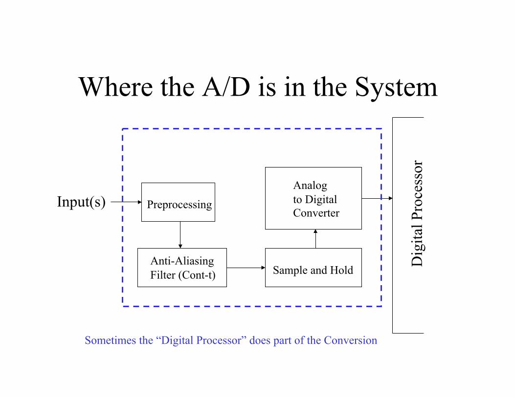
Where the A/D is in the System
Preprocessing
Anti-Aliasing Filter (Cont-t) Sample and Hold
Analog to Digital Converter
Dig
ital P
roce
ssor
Input(s)
Sometimes the “Digital Processor” does part of the Conversion

Types of A/D Converters Conversion Rate Nyquist ADCs Oversampled ADCs
Slow Integrating (Serial) Very high resolution >14 bits
Medium Successive Approximation 1-bit Pipeline Algorithmic
Moderate resolution >10 bits
Fast Flash Multiple-bit Pipeline
Folding and interpolating
Low resolution > 6 bits

Ideal input-output characteristics of a 3-bit DAC
1.000
0.875
0.750
0.625
0.500
0.375
0.250
0.125
0.000
Ana
log
Out
put V
alue
Nor
mal
ized
to VRE
F
000 001 010 011 100 101 110 111Digital Input Code
Vertical ShiftedCharacteristic
Infinite ResolutionCharacteristic
1 LSB
Fig. 10.1-4

D/A Definitions
DigitalInput Code
0LSB
0.5LSB
1LSB
-0.5LSB
000 001 010 011 100 101 110 111
Quantization Noise
Fig. 10.1-5
Quantization Noise is the inherent uncertainty in digitizing an analog value with a finite resolution converter.
Resolution of the DAC is equal to the number of bits in the applied digital input word.

A/D Definitions The dynamic range, signal-to-noise ratio (SNR), and the effective number of bits (ENOB) of the ADC are the same as for the DAC
Resolution of the ADC is the smallest analog change that can be distinguished by an ADC.
Quantization Noise is the ±0.5LSB uncertainty between the infinite resolution characteristic and the actual characteristic.

Ideal input-output
characteristics of a 3-bit ADC
Analog Input Value Normalized to VREF
000
001
010
011
100
101
110
111
Dig
ital O
utpu
t Cod
e
Ideal 3-bitCharacteristic
Figure 10.5-3 Ideal input-output characteristics of a 3-bit ADC.
Infinite ResolutionCharacteristic
1 LSB
18
28
38
48
58
68
08
78
1 LSB
vinVREF
0.51.0
0.0-0.5Q
uant
izat
ion
Noi
se L
SBs
88

Types of Encodings in A/Ds
Table 10.5-2 - Digital Output Codes used for ADCs
Decimal Binary Thermometer Gray Two’s Complement
0 000 0000000 000 000
1 001 0000001 001 111
2 010 0000011 011 110
3 011 0000111 010 101
4 100 0001111 110 100
5 101 0011111 111 011
6 110 0111111 101 010
7 111 1111111 100 001

Testing of D/A Converters
Sweep the digital input word from 000...0 to 111...1.
The ADC should have more resolution by at least 2 bits and be more accurate than the errors of the DAC
INL will show up in the output as the presence of 1’s in any bit. If there is a 1 in the Nth bit, the INL is greater than ±0.5LSB
DNL will show up as a change between each successive digital error output.
The bits which are greater than N in the digital error output can be used to resolve the errors to less than ±0.5LSB
N-bitDACunder test
ADC withmore resolution
than DAC(N+2 bits)
DigitalSubtractor(N+2 bits)
DigitalWordInput
(N+2 bits)
Vout
ADCOutput Digital
ErrorOutput
(N+2 bits)
Fig. 10.1-9
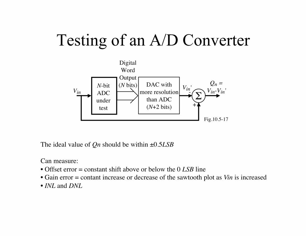
Testing of an A/D Converter
N-bitADCunder test
DAC withmore resolution
than ADC(N+2 bits)
DigitalWord
Output(N bits)
Fig.10.5-17
Vin Y-
+
Vin'Qn =
Vin-Vin'
The ideal value of Qn should be within ±0.5LSB
Can measure: • Offset error = constant shift above or below the 0 LSB line • Gain error = contant increase or decrease of the sawtooth plot as Vin is increased • INL and DNL
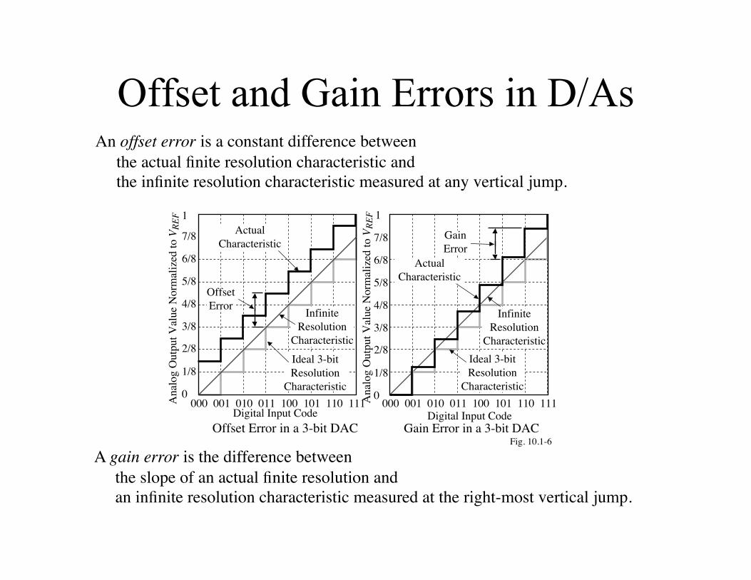
Offset and Gain Errors in D/As An offset error is a constant difference between the actual finite resolution characteristic and the infinite resolution characteristic measured at any vertical jump.
Gain Error in a 3-bit DACOffset Error in a 3-bit DAC
Ana
log
Out
put V
alue
Nor
mal
ized
to VRE
F
000 001 010 011 100 101 110 111Digital Input Code
Ideal 3-bitResolution
Characteristic
1
7/8
6/8
5/8
4/8
3/8
2/8
1/8
0
Actual Characteristic
GainError
InfiniteResolution
Characteristic
Ana
log
Out
put V
alue
Nor
mal
ized
to VRE
F
000 001 010 011 100 101 110 111Digital Input Code
OffsetError
1
7/8
6/8
5/8
4/8
3/8
2/8
1/8
0
Actual Characteristic
InfiniteResolution
CharacteristicIdeal 3-bitResolution
Characteristic
Fig. 10.1-6
A gain error is the difference between the slope of an actual finite resolution and an infinite resolution characteristic measured at the right-most vertical jump.

Offset and Gain Errors in A/Ds
000
001
010
011
100
101
110
111
vinVREF
Dig
ital O
utpu
t Cod
e
Offset = 1.5 LSBs
000
001
010
011
100
101
110
111
08
18
28
38
48
58
68
78
88
vinVREF
Dig
ital O
utpu
t Cod
e
Gain Error = 1.5LSBs
(a.) (b.)Figure 10.5-4 - (a.) Example of offset error for a 3-bit ADC. (b.) Example of gainerror for a 3-bit ADC.
IdealCharacteristic
IdealCharacteristic
08
18
28
38
48
58
68
78
88
ActualCharacteristic
Offset Error is the horizontal difference between the ideal finite resolution characteristic and actual finite resolution characteristic
Gain Error is the horizontal difference between the ideal finite resolution characteristic and actual finite resolution characteristic which is proportional to the analog input voltage.

Monotonicity
000
001
010
011
100
101
110
111
08
18
28
38
48
58
68
78
88
vinVREF
Dig
ital O
utpu
t Cod
e
DNL =-2 LSB
ActualCharacteristic
IdealCharacteristic
Fig. 10.5-6L
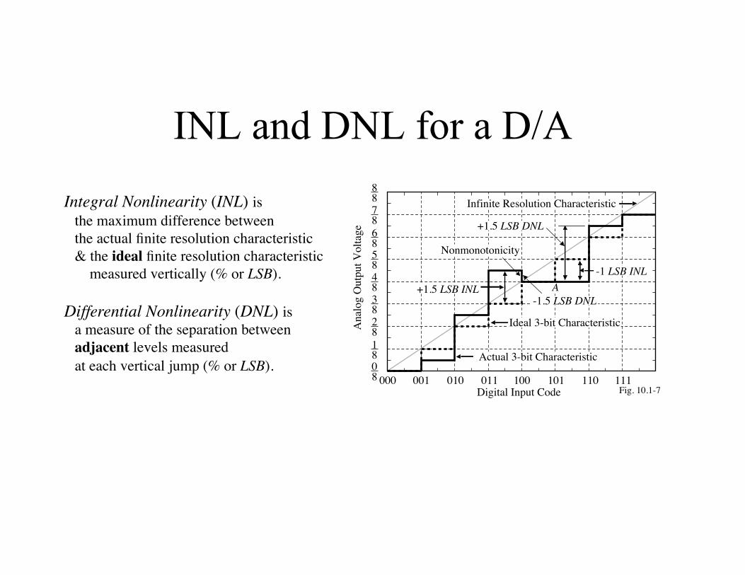
INL and DNL for a D/A
000 001 010 011 100 101 110 111
1808
28
38
48
58
68
78
88
Ana
log
Out
put V
olta
ge
Digital Input Code
Ideal 3-bit Characteristic
Actual 3-bit Characteristic
Infinite Resolution Characteristic
+1.5 LSB INL-1 LSB INL
+1.5 LSB DNL
A-1.5 LSB DNL
Nonmonotonicity
Fig. 10.1-7
Integral Nonlinearity (INL) is the maximum difference between the actual finite resolution characteristic & the ideal finite resolution characteristic measured vertically (% or LSB).
Differential Nonlinearity (DNL) is a measure of the separation between adjacent levels measured at each vertical jump (% or LSB).

Example of INL and DNL of a
Nonideal 4-bit DAC
15/16
14/16
13.16
12/16
11/16
10/16
9/16
8/16
7/16
6/16
5/16
4/16
3/16
2/16
1/160/16
0 10 0 0 0 0 0 0 1 1 1 1 1 1 10 0 0 0 1 1 1 1 0 0 0 0 1 1 1 10 0 1 1 0 0 1 1 0 0 1 1 0 0 1 10 1 0 1 0 1 0 1 0 1 0 1 0 1 0 1
b1b2b3b4
Ana
log
Out
put (
Nor
mal
ized
to F
ull S
cale
)
Digital Input Code
-1.5 LSB INL
-2 LSB DNL
Actual 4-bit DACCharacteristic
+1.5 LSB DNL
+1.5 LSB INL
Ideal 4-bit DACCharacteristic
-2 LSB DNL
Fig. 10.1-8

INL and DNL of a 3-bit ADC
000
001
010
011
100
101
110
111
08
18
28
38
48
58
68
78
88
vinVREF
Dig
ital O
utpu
t Cod
e
DNL =-2 LSB
ActualCharacteristic
IdealCharacteristic
Fig. 10.5-6DL
INL =+1LSB
INL =-2LSB
DNL =+1 LSB
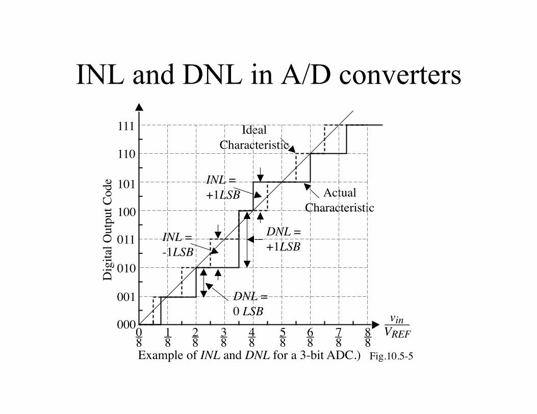
INL and DNL in A/D converters
000
001
010
011
100
101
110
111
08
18
28
38
48
58
68
78
88
vinVREF
Dig
ital O
utpu
t Cod
e
Example of INL and DNL for a 3-bit ADC.) Fig.10.5-5
IdealCharacteristic
ActualCharacteristic
INL =+1LSB
INL =-1LSB
DNL =+1LSB
DNL =0 LSB

Dynamic Testing of D/A Converters
N-bitDACunder test
DigitalPattern
Generator(N bits)
Vout
Clock
DistortionAnalyzer
Vout
t
|Vout(jt)|
tfsig
SpectralOutput
1000
0
1000
1
1001
1
1111
1
Noise floordue to non-linearities
VREF
Fig. 10.1-10
All nonlinearities of the DAC (i.e. INL and DNL) will cause harmonics of the fundamental frequency
The THD can be used to determine the SNR dB range between the magnitude of the fundamental and the THD. This SNR should be at least 6N dB to have an INL of less than ±0.5LSB for an ENOB of N-bits.
If the period of the digital pattern is increased, the frequency dependence of INL can be measured.
Note that the noise contribution of VREF must be less than the noise floor due to nonlinearities.
Digital input pattern is selected to have a fundamental frequency which has a magnitude of at least 6N dB above its harmonics. Length of the digital sequence determines the spectral purity of the fundamental frequency.