the low power analogue and digital baseband processing parts of a novel multimode dect/gsm/dcs1800...
TRANSCRIPT
The low power analogue and digital baseband processing parts
of a novel multimode DECT/GSM/DCS1800 terminal
C. Drososa, C. Drea, D. Metafasa, D. Soudrisb,*, S. Blionasa
aINTRACOM S.A., Hellenic Telecommunications and Electronics Industry, Peania 19002, GreecebDepartment of Electrical and Computer Engineering, VLSI Design Testing Center, Democritus University of Thrace, 67100 Xanthi, Greece
Received 25 September 2003; revised 23 January 2004; accepted 11 February 2004
Abstract
In order to support a multimode DECT/GSM/DCS1800 terminal architecture, with low power characteristics and integrated support for
direct conversion terminal architecture, the critical parts of such a terminal were designed and implemented using three different chips.
These parts include a baseband processor, a modem and suitable analogue parts. The baseband processor was designed to support multimode
operation, all baseband processing required and different terminal architectures (heterodyne or direct conversion). The modem features a
GMSK/GFSK modulator and a novel, low power detection algorithm supports a direct conversion terminal. The analogue circuitry includes
analogue filters and Digital-to-Analog and Analog-to-Digital converters. The architecture of the direct conversion wireless terminal is
presented along with details on the low power characteristics of the processor and the modem. Experimental results from the operation of the
multimode terminal are presented.
q 2004 Elsevier Ltd. All rights reserved.
Keywords: DECT/GSM/DCS1800 terminal; Analogue and digital baseband; Direct conversion; GFSK/GMSK modem; Processor architecture
1. Introduction
The majority of wireless terminals offer services and
support for a single telecommunication standard, such as
DECT or GSM. DECT is basically a radio access
technology, while GSM is a digital cellular technology
with support for mobility. Nowadays, multi-mode terminals
that support DECT services (voice, 64 kbps data) in DECT
coverage areas and GSM services (voice, SMS, 9.6 kbps
data or even more) in GSM/DCS-1800 coverage areas are an
interesting solution that offers flexibility and opens the road
to many new attractive services [1]. In order to combine the
advantages and the services offered by each standard, DECT
and GSM, the idea of a multimode wireless terminal
becomes self-evident. Besides their functional character-
istics, these terminals should exhibit small size and long
autonomous operation and therefore, the low-power design
becomes an interesting and challenging design issue.
There are three basic ways to combine DECT systems
with GSM, allowing different kind of services:
† using a dual-mode DECT/GSM handset where the DECT
and GSM fixed systems are not interconnected;
† connecting a DECT fixed system to a GSM system
(GSM900, DCS1800 or PCS1900) through its base
station controller interface;
† connecting a DECT fixed system to a GSM system
through an enhanced ISDN interface.
All three ways offer different levels of integration and
provide alternative ways to take advantage of the combi-
nation of DECT and GSM into a single terminal. More
details on the DECT and GSM interworking scenarios and
supported services can be found in Ref. [1].
In order to achieve the above target the first leg of the
solution was the design and implementation of a baseband
processor capable to implement all baseband processing
required by both standards. The designed baseband
processor, one of the three chips of the terminal, integrates
all required DECT and GSM/DCS1800 functionality and has
0026-2692/$ - see front matter q 2004 Elsevier Ltd. All rights reserved.
doi:10.1016/j.mejo.2004.02.002
Microelectronics Journal 35 (2004) 609–620
www.elsevier.com/locate/mejo
* Corresponding author. Tel.: þ30-25410-795-57; fax: þ30-254-10-
79-545.
E-mail address: [email protected] (D. Soudris).
built-in support for different terminal architectures for
achieving maximum flexibility. To the best of our
knowledge, the implemented processor is the first single
chip solution of a multimode terminal.
The solution to the problems of today’s heterodyne
receiver, such as the amount of circuits and the increased
power consumption, is the direct conversion terminal
architecture [2]. Furthermore, if it is combined with an
innovative low power, low complexity direct conversion
detection algorithm the gain becomes even bigger [3].
This detection algorithm has been implemented inside the
multimode modem.
Apart from the novel DECT/GSM baseband processor,
the purpose of this paper is to present the other analogue and
digital baseband parts of a multimode wireless terminal,
which supports DECT and GSM/DCS1800 operations
seamlessly. These baseband parts from the system’s point
of view also include the modem, which contains
modulators, detectors and digital filters and the analogue
parts of the terminal, which includes converters and
analogue filters. Both the modem and the analogue parts
must support multimode operation to reduce the complexity
of the multimode terminal. As far as the RF parts of the
multimode terminal are concerned [4,5], these are
considered out of the scope of this paper, so only the
analogue and digital baseband parts will be presented in the
following sections.
The main contribution of this paper is the presentation of
a complete integrated system, which is the first implemen-
tation in the literature. The purpose of this paper is to
present a system-level approach of the designed multimode
terminal. Our scope is to provide only the critical
information from each component of the terminal, while
in-depth technical information can be found in appropriate
cited work. The main design achievements and innovations
of each component are also described.
Comparing the proposed multimode solution with an
individual chipset implementation of each standard [6],
it can be deduced that the proposed solution has a big
advantage because it occupies smaller area on the terminal’s
board than the solution with separate GSM and DECT
chipsets (TI’s TCS2600 chipset—OMAP730, TWL3016
and TRF6151—for GSM and CVM chipset of National
Semiconductors for DECT—SC14428 and LMX4168—a
total of 5 chips for a DECT/GSM terminal). This influences
the size and the cost of final terminal significantly.
This paper is organized as follows; Section 2
describes the multimode DECT-GSM/DCS1800 terminal,
Section 3 the baseband processor and Section 4 the modem.
The analogue baseband parts of the multimode terminal are
presented in Section 5. Testing results of the developed
terminal are presented in Section 6, while the final
conclusions are in Section 7.
2. Dual-mode terminal architecture
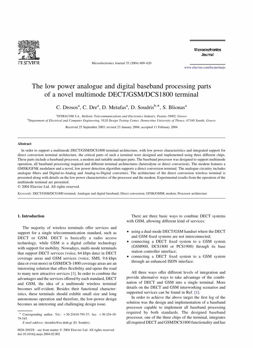
Fig. 1 presents the main building architectural blocks of
the multi-mode direct conversion terminal. It basically
consists of the DECT/GSM baseband processor (named
ASPIS processor), the multimode low power DECT/GSM
modem and the required analogue circuits. The function,
the architectural design and the physical implementation of
the above building blocks under the context of the
multimode terminal will be presented in the following
paragraphs.
Apart from the digital and analogue baseband parts,
which comprise the system’s view of the multimode
terminal, Fig. 1 also presents the RF part of the DECT/
GSM terminal. The brief presentation of the RF part in the
following paragraphs targets only to a more concrete
overview of the system, since the RF part’s description is
beyond of the scope of this paper.
At the transmit path, the ASPIS processor prepares the
DECT or GSM transmit burst and creates the suitable
control signals to transfer this burst to the transmit path of
Fig. 1. Multimode terminal architecture.
C. Drosos et al. / Microelectronics Journal 35 (2004) 609–620610
the multimode modem. The transmitted burst can contain
either data or digitised voice samples that are encoded by a
Digital Signal Processor (DSP) inside the ASPIS processor.
The data bits that comprise the DECT/GSM slot are input to
the modem for digital GMSK (Gaussian Minimum Shift
Keying) or GFSK (Gaussian Frequency Shift Keying)
modulation. The produced 10-bit I and Q signals are then
passed to the baseband board to a twin Tx Digital-to-Analog
(DAC) and the analogue reconstruction filters. The output of
this analogue baseband block is then passed to the RF board
for direct up-conversion, power amplification and
transmission. The frequency synthesiser is programmed to
the proper frequency channel by the ASPIS processor.
At the receive path, the RF signal is mixed with the
channel frequency provided by the synthesiser and is
converted to baseband. The baseband signal produces
In phase and Quadrature signals (I and Q signals) after
processing by a quadrature demodulator. These signals are
then filtered by low pass filters for anti-aliasing purposes
and then amplified by a variable gain amplifier, just before
the digitisation of the signal. Then, the signal is converted to
digital and processed by the custom designed FIR filters of
the modem, which perform the channel selection filtering.
The detection of the data bits from the I and Q signals is
realised by a hardware implementation of a phase detector
inside the multimode modem. The implemented algorithm
performs also timing recovery and automatic frequency
offset correction to compensate for frequency differences
with the local oscillator of the transmitter. Another module
inside the modem is responsible for the estimation of the DC
offset and corrects the I and Q signals before they are
processed by the detector. This correction takes place in
both the digital and analogue paths of the received signals.
Finally, the modem’s detector circuit sends the ASPIS
processor valid demodulated data. The ASPIS processor is
responsible for the speech decoding (ADPCM in DECT,
Full Rate Vocoder in GSM operation), which is performed
in an application specific instruction set DSP processor.
3. Digital baseband processor
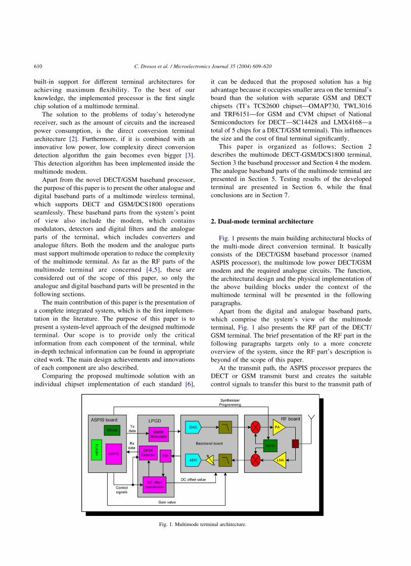
The baseband (or ASPIS) processor is based on a
multi-processor System-on-Chip (SoC) architecture. It is
capable to implement all the baseband signal processing
required in a multi-mode terminal, the protocol stacks for
the DECT and GSM/DCS-1800, the application layer, as
well as the overall control of the operation of a complete
multimode DECT/GSM handset. A detailed view of the
ASPIS processor’s internal architecture is presented in
Fig. 2. The ASPIS processor is the first and the only existing
multi-mode baseband processor available for DECT and
GSM/DCS1800 wireless terminals implemented as a SoC
into a one-chip terminal solution [7].
The ASPIS SoC is build around an internal system bus
with 32 bits width for the data bus and 24 bits for the address
bus. The ARM7TDMI [8] core is one of the masters of this
bus, and it is responsible for the execution of the upper
layers of the protocols, the application and the overall
control of the operation of the multimode terminal. Its
operation is enhanced by the use of a dedicated internal
memory area for efficient program and data storage.
Communication protocol execution is also assisted by
dedicated logic co-processors that perform specific func-
tionality. The two most important of these co-processors
Fig. 2. ASPIS SoC hardware architecture.
C. Drosos et al. / Microelectronics Journal 35 (2004) 609–620 611
are the Audio I/F and the RF I/F, that is a DECT/GSM
physical layer processor.
Some special system functions are performed by an
application specific instruction set 16-bit DSP processor.
A custom-optimised DSP processor (Application Specific
Instruction set Processor—ASIP) handles the heavy func-
tions required by DECT and GSM, such as voice processing
and radio signal equalisation and includes custom
instructions for accelerating the computing intensive base-
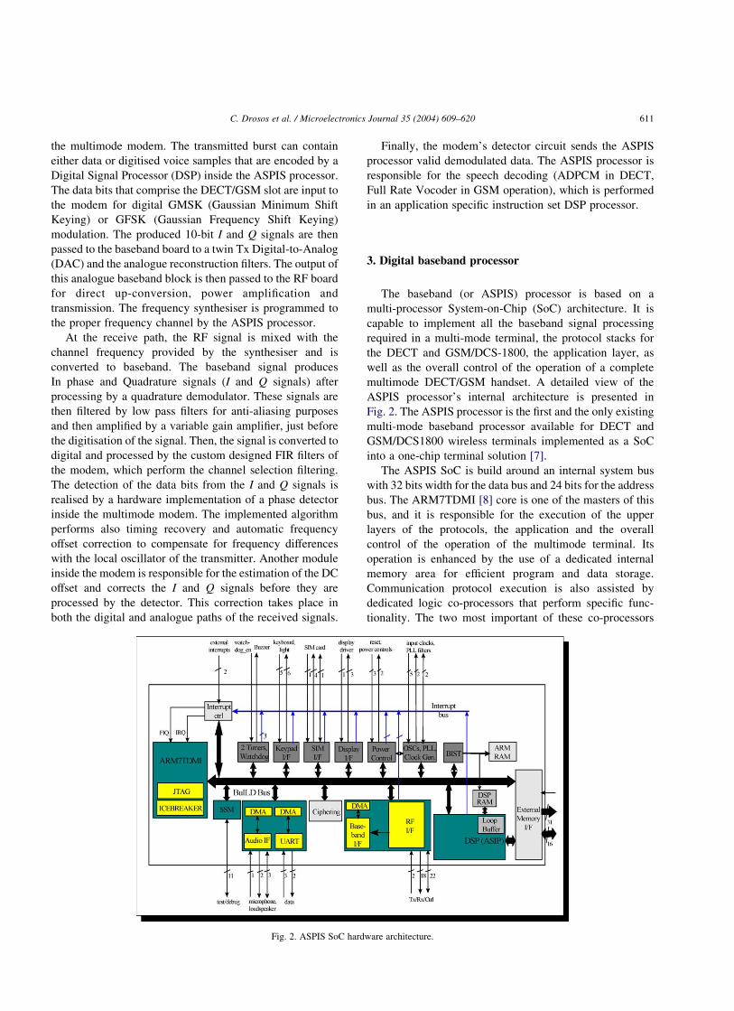
band processing functions [9]. The custom DSP architec-
ture, Fig. 3, is composed of four basic stages organized in a
pipelined fashion. The first three stages are the Instruction
Fetch, Decode and Execution. The latter stage provides also
forwarding mechanisms for overcoming data dependencies
resulting from the consecutive instruction execution in the
pipeline. The last stage is the Write Back that stores
the result of the previous operation to the corresponding
destination register.
This DSP processor was designed according to the
specifications and the requirements of the DECT/GSM
operation and includes custom instructions that are
specialised in acceleration of the execution of the GSM
equalisation and the voice codecs, ADPCM in DECT,
full rate voice codec in GSM. The DSP core is not a master
to the internal system bus of the ASPIS chip. This was
dictated by the need of the ARM processor to fully utilise
the internal bus, without sharing it with other processor type
masters. On the other hand, it has direct access to the
external memory through the External Memory Interface
(EMI) module. Furthermore, a special dedicated internal
memory area is used as data cache of the DSP, which also
incorporates a dedicated loop buffer that is used as an
instruction cache during the execution of the body of a loop.
The EMI co-processor shares the external memory
resource between the DSP core and the current master of
the internal bus (ARM, Audio I/F or RF I/F). A special
arbitration scheme is utilised in order to share efficiently
the external memory and to avoid memory starvation.
This arbitration scheme is programmable, by the ARM core,
which can at any time modify the percentage of the memory
bandwidth that is shared between the DSP and the system
bus masters.
The rest of the co-processors are modules performing a
specific protocol oriented or protocol accelerating function-
ality or interface elements of the ASPIS system, such as the
SIM interface, the Buzzer, the LCD interface, the Keypad
interface, the Timers, the Interrupt Controller and the
Watchdog.
An ad hoc strategy was adopted for the integration of the
diverse testing strategies that are used in the ASPIS
processor [10]. The strategy adopted for the testing is a
non-scan-based technique, exploiting the high bandwidth
and control features of the chip’s internal bus. As a result,
support circuitry and procedures are included for testing of
individual components via the system bus. This method
features excellent fault-coverage with a circuit overhead
that compares favourably with scan-path based methods.
An advanced co-simulation methodology has been
undertaken during the development of the ASPIS processor
and its corresponding software libraries [11]. Two
co-simulation environments have been developed: a low-
level VHDL co-simulation environment and, an advanced
high-level software model of the ASPIS processor to be used
within the instruction set simulator tool of the ARM core.
The ASPIS processor was designed entirely in VHDL and
fabricated as a single embedded gate array. The operating
voltage is 3.3 V and its package is a 208-lead plastic QFP
with a size of 28 £ 28 £ 3.4 mm. The technology used was
Mitel’s cla200 at 0.35 mm. The developed random logic for
the ASPIS peripherals equals to 200,000 gates, while the total
gate count of the chip is 280,000 equivalent gates.
The maximum power dissipation of the ASPIS processor is
Fig. 3. Custom DSP core architecture.
C. Drosos et al. / Microelectronics Journal 35 (2004) 609–620612
250 mW, while the maximum design operating frequency is
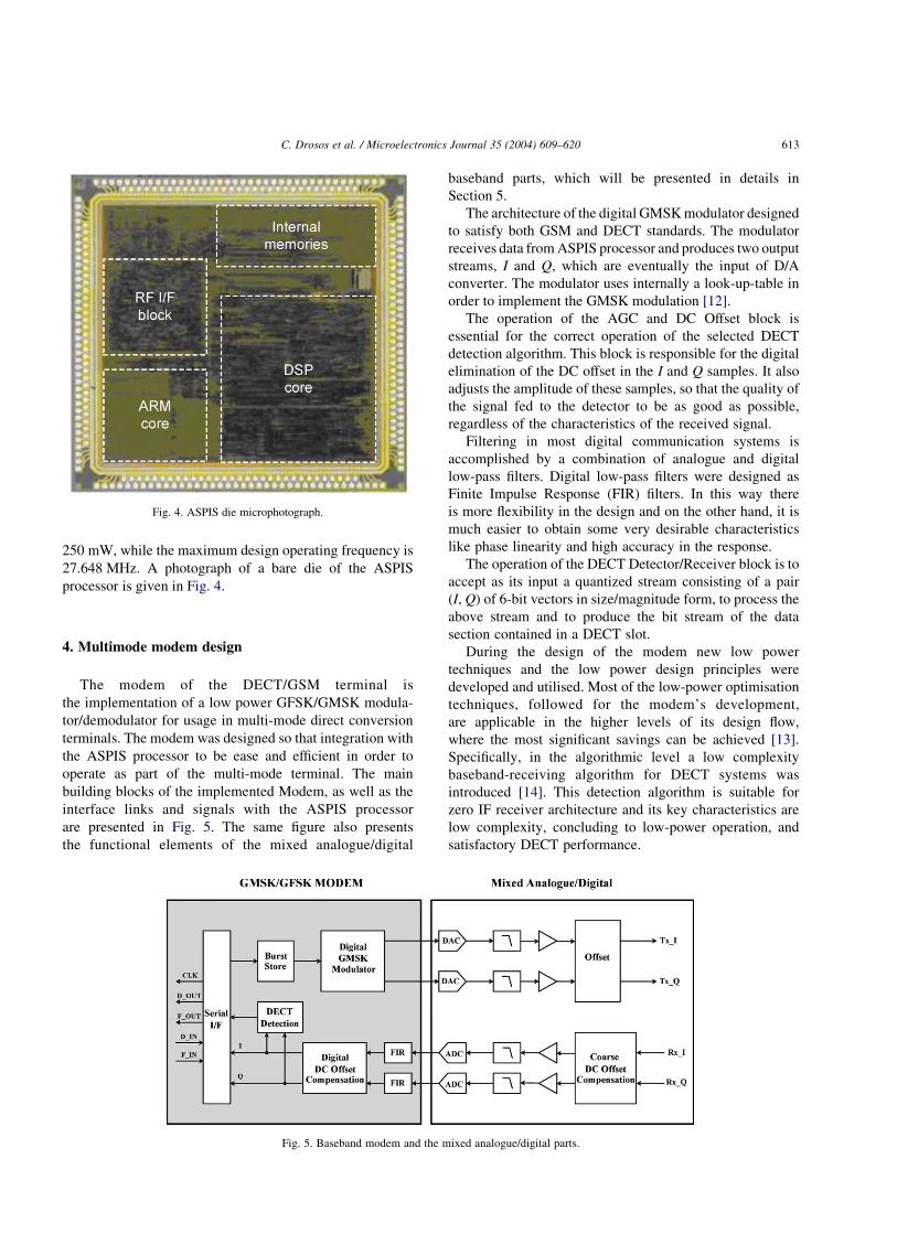
27.648 MHz. A photograph of a bare die of the ASPIS
processor is given in Fig. 4.
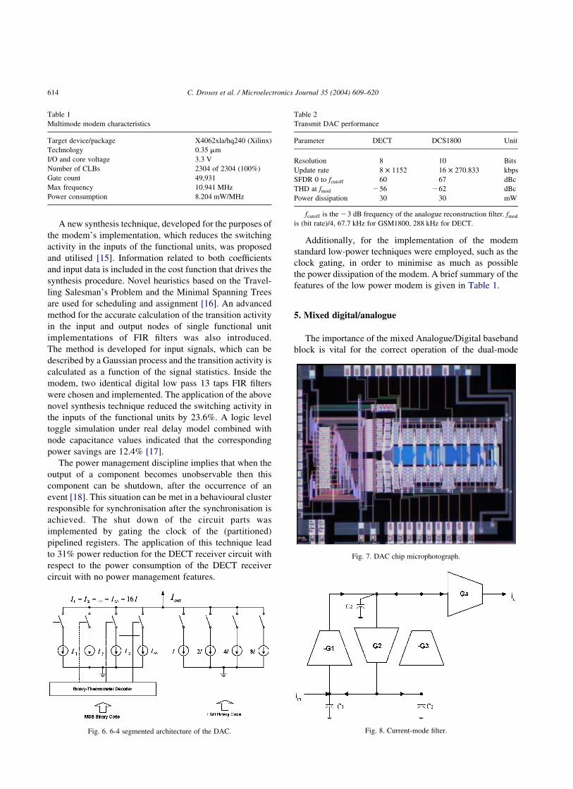
4. Multimode modem design
The modem of the DECT/GSM terminal is
the implementation of a low power GFSK/GMSK modula-
tor/demodulator for usage in multi-mode direct conversion
terminals. The modem was designed so that integration with
the ASPIS processor to be ease and efficient in order to
operate as part of the multi-mode terminal. The main
building blocks of the implemented Modem, as well as the
interface links and signals with the ASPIS processor
are presented in Fig. 5. The same figure also presents
the functional elements of the mixed analogue/digital
baseband parts, which will be presented in details in
Section 5.
The architecture of the digital GMSK modulator designed
to satisfy both GSM and DECT standards. The modulator
receives data from ASPIS processor and produces two output
streams, I and Q, which are eventually the input of D/A
converter. The modulator uses internally a look-up-table in
order to implement the GMSK modulation [12].
The operation of the AGC and DC Offset block is
essential for the correct operation of the selected DECT
detection algorithm. This block is responsible for the digital
elimination of the DC offset in the I and Q samples. It also
adjusts the amplitude of these samples, so that the quality of
the signal fed to the detector to be as good as possible,
regardless of the characteristics of the received signal.
Filtering in most digital communication systems is
accomplished by a combination of analogue and digital
low-pass filters. Digital low-pass filters were designed as
Finite Impulse Response (FIR) filters. In this way there
is more flexibility in the design and on the other hand, it is
much easier to obtain some very desirable characteristics
like phase linearity and high accuracy in the response.
The operation of the DECT Detector/Receiver block is to
accept as its input a quantized stream consisting of a pair
(I, Q) of 6-bit vectors in size/magnitude form, to process the
above stream and to produce the bit stream of the data
section contained in a DECT slot.
During the design of the modem new low power
techniques and the low power design principles were
developed and utilised. Most of the low-power optimisation
techniques, followed for the modem’s development,
are applicable in the higher levels of its design flow,
where the most significant savings can be achieved [13].
Specifically, in the algorithmic level a low complexity
baseband-receiving algorithm for DECT systems was
introduced [14]. This detection algorithm is suitable for
zero IF receiver architecture and its key characteristics are
low complexity, concluding to low-power operation, and
satisfactory DECT performance.
Fig. 5. Baseband modem and the mixed analogue/digital parts.
Fig. 4. ASPIS die microphotograph.
C. Drosos et al. / Microelectronics Journal 35 (2004) 609–620 613
A new synthesis technique, developed for the purposes of
the modem’s implementation, which reduces the switching
activity in the inputs of the functional units, was proposed
and utilised [15]. Information related to both coefficients
and input data is included in the cost function that drives the
synthesis procedure. Novel heuristics based on the Travel-
ling Salesman’s Problem and the Minimal Spanning Trees
are used for scheduling and assignment [16]. An advanced
method for the accurate calculation of the transition activity
in the input and output nodes of single functional unit
implementations of FIR filters was also introduced.
The method is developed for input signals, which can be
described by a Gaussian process and the transition activity is
calculated as a function of the signal statistics. Inside the
modem, two identical digital low pass 13 taps FIR filters
were chosen and implemented. The application of the above
novel synthesis technique reduced the switching activity in
the inputs of the functional units by 23.6%. A logic level
toggle simulation under real delay model combined with
node capacitance values indicated that the corresponding
power savings are 12.4% [17].
The power management discipline implies that when the
output of a component becomes unobservable then this
component can be shutdown, after the occurrence of an
event [18]. This situation can be met in a behavioural cluster
responsible for synchronisation after the synchronisation is
achieved. The shut down of the circuit parts was
implemented by gating the clock of the (partitioned)
pipelined registers. The application of this technique lead
to 31% power reduction for the DECT receiver circuit with
respect to the power consumption of the DECT receiver
circuit with no power management features.
Additionally, for the implementation of the modem
standard low-power techniques were employed, such as the
clock gating, in order to minimise as much as possible
the power dissipation of the modem. A brief summary of the
features of the low power modem is given in Table 1.
5. Mixed digital/analogue
The importance of the mixed Analogue/Digital baseband
block is vital for the correct operation of the dual-mode
Table 1
Multimode modem characteristics
Target device/package X4062xla/hq240 (Xilinx)
Technology 0.35 mm
I/O and core voltage 3.3 V
Number of CLBs 2304 of 2304 (100%)
Gate count 49,931
Max frequency 10.941 MHz
Power consumption 8.204 mW/MHz
Fig. 6. 6-4 segmented architecture of the DAC.
Table 2
Transmit DAC performance
Parameter DECT DCS1800 Unit
Resolution 8 10 Bits
Update rate 8 £ 1152 16 £ 270.833 kbps
SFDR 0 to fcutoff 60 67 dBc
THD at fmod 256 262 dBc
Power dissipation 30 30 mW
fcutoff is the 23 dB frequency of the analogue reconstruction filter. fmod
is (bit rate)/4, 67.7 kHz for GSM1800, 288 kHz for DECT.
Fig. 7. DAC chip microphotograph.
Fig. 8. Current-mode filter.
C. Drosos et al. / Microelectronics Journal 35 (2004) 609–620614
modem, and as a result, for the overall performance of the
dual-mode terminal. Its main parts are: (i) the analogue
filters and (ii) the DA and AD converters (DAC/ADC).
A graphical overview of these blocks can be found in Fig. 5,
along with the general context of the baseband chain in
which they are used. All these analogue cells have been
implemented in a standard 3.3 V 0.8 mm CMOS technology
provided by AMS [19]. The scope of these mixed analogue
and digital parts was to implement a flexible baseband
interface for a DECT/GSM1800 direct conversion trans-
ceiver, in a low cost digital technology using current-mode
techniques.
The Tx module accepts digital GMSK or GFSK I and Q
waveforms generated by the digital GMSK/GFSK modu-
lator and performs the DA conversion and analogue
reconstruction of the signals so that they can be upconverted
and transmitted using a quadrature modulator. The Rx part,
accepts analogue GMSK/GFSK I and Q waveforms
generated by a quadrature demodulator and performs anti-
alias filtering and A/D conversion.
5.1. Digital-to-analog converter
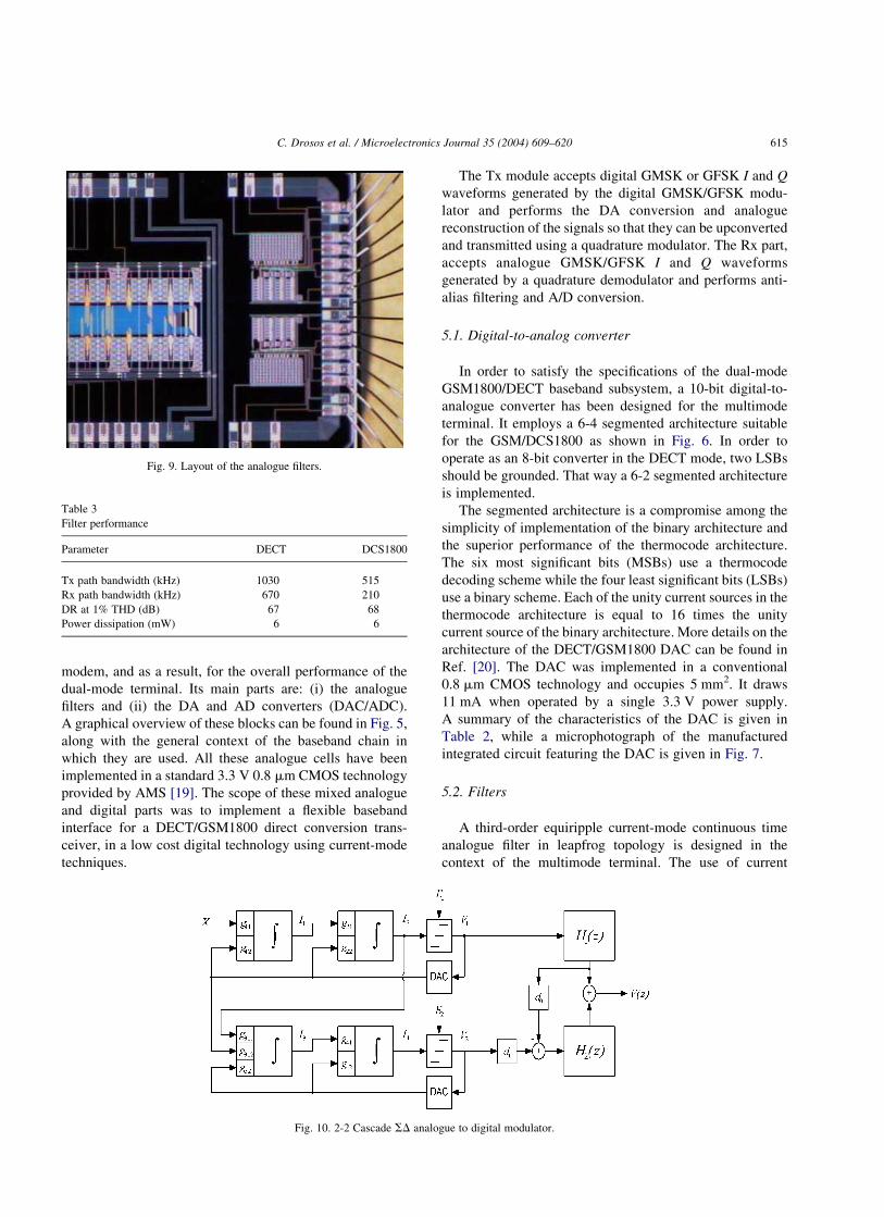
In order to satisfy the specifications of the dual-mode
GSM1800/DECT baseband subsystem, a 10-bit digital-to-
analogue converter has been designed for the multimode
terminal. It employs a 6-4 segmented architecture suitable
for the GSM/DCS1800 as shown in Fig. 6. In order to
operate as an 8-bit converter in the DECT mode, two LSBs
should be grounded. That way a 6-2 segmented architecture
is implemented.
The segmented architecture is a compromise among the
simplicity of implementation of the binary architecture and
the superior performance of the thermocode architecture.
The six most significant bits (MSBs) use a thermocode
decoding scheme while the four least significant bits (LSBs)
use a binary scheme. Each of the unity current sources in the
thermocode architecture is equal to 16 times the unity
current source of the binary architecture. More details on the
architecture of the DECT/GSM1800 DAC can be found in
Ref. [20]. The DAC was implemented in a conventional
0.8 mm CMOS technology and occupies 5 mm2. It draws
11 mA when operated by a single 3.3 V power supply.
A summary of the characteristics of the DAC is given in
Table 2, while a microphotograph of the manufactured
integrated circuit featuring the DAC is given in Fig. 7.
5.2. Filters
A third-order equiripple current-mode continuous time
analogue filter in leapfrog topology is designed in the
context of the multimode terminal. The use of current
Table 3
Filter performance
Parameter DECT DCS1800
Tx path bandwidth (kHz) 1030 515
Rx path bandwidth (kHz) 670 210
DR at 1% THD (dB) 67 68
Power dissipation (mW) 6 6
Fig. 9. Layout of the analogue filters.
Fig. 10. 2-2 Cascade SD analogue to digital modulator.
C. Drosos et al. / Microelectronics Journal 35 (2004) 609–620 615
mode filters offers significant advantages in the design of the
terminal, since this they can tolerate higher input signals and
present lower intermodulation products [21]. The system
specifications have been derived in such manner so that the
same filter topology, shown in Fig. 8, can be used in both
receive and transmit path and in both GSM1800 and DECT
modes. More details on the design of the filters can be
found in Ref. [20]. Frequency tuning is accomplished by
switching capacitors from an array of matched MOS
capacitor structures. The filters have been implemented in
a conventional 0.8 mm CMOS technology by AMS, the total
power dissipation is less than 6 mW in a single 3.3 V power
supply and they occupy approximately 0.5 mm2 of die area.
The analogue filters’ layout is shown in the upper right part
of Fig. 9.
A brief presentation of all the implemented features of
the signal reconstruction analogue filters is given in Table 3.
5.3. Analogue-to-digital converter
The ADC was implemented as a SD modulator. Besides
using low cost technologies for the terminal’s implemen-
tation, the SD approach fits very well in the multi-standard
receiver concept where e.g. different resolution require-
ments for various signal bandwidths can be met with just a
simple change in the sampling frequency. The final
implementation choice was a MASH 2-2 architecture [22],
presented in Fig. 10, which is more modular to implement
and requires less complex digital error correction network
Table 4
Receive ADC performance
Parameter DECT DCS1800
Resolution (bits) 8@100 kHz 12@650 kHz
Update Rate (KHz) 16 £ 1152 32 £ 270.833
SFDR (dB) 30 40
SNR (dB) 50 70
Fig. 11. Microphotograph of ADC’s die.
Fig. 12. Modulator spectrum in DECT mode.
C. Drosos et al. / Microelectronics Journal 35 (2004) 609–620616
than alternative architectures that utilise cascade structures
of first order modulators. Specific details on the character-
istics and the design of the ADC can be found in Ref. [23].
The ADC was implemented in a conventional 0.8 mm
CMOS technology and occupies 7 mm2. The power
dissipation, at 3.3 V power supply, is 75 mW for
the analogue part and 20 mW for the digital part when
used in DECT mode. In GSM mode the power falls to
45 mW for the analogue and 13 mW for the digital part,
respectively. Performance figures for the ADC can be found
in Table 4, while a microphotograph of the ADC’s die is
given in Fig. 11.
6. Testing results
Exhaustive testing proved the correctness of the direct
conversion multimode wireless terminal based on the
ASPIS and the modem modules and more specifically
the innovative low power detection algorithm. Furthermore,
the analogue parts were exhaustively tested to
verify compliance to both standards, DECT and
GSM1800. A set of representative experimental results is
presented here.
Fig. 12 displays the spectrum of the generated I and Q
signal from the modulator in DECT mode. This spectrum
produced after filtering with the anti-image Bessel filters
that are part of the multimode terminal. The maximum
power levels as specified by ETSI for the adjacent
channels are also shown. It is clear that the filtered output
signal satisfies the maximum power levels.
A number of bit error rate (BER) measurements have been
performed in order to evaluate the performance of the
modem’s novel direct conversion receiver. As an example,
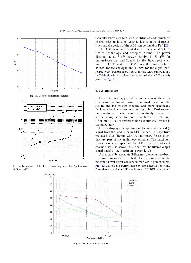
Fig. 13 depicts the performance of the detector for white
Gaussian noise channel. The reference 1023 BER is achieved
Fig. 13. Detector performance reference.
Fig. 14. Performance of the detector over frequency offset (perfect sync,
SNR ¼ 12 dB).
Fig. 15. SFDR vs. fout at 10 MS/s.
C. Drosos et al. / Microelectronics Journal 35 (2004) 609–620 617
for a signal to noise ratio (SNR) of 10.5 dB.
These measurements were performed with the FIRs filters
enabled in the modem’s receiver path. Without these filters,
there is a degradation of the measured SNR by 4 dBs.
The performance of the detection algorithm inside the
receiver of the modem was also tested against frequency
offsets. Results are displayed in Fig. 14 and prove that
frequency offsets up to DfT ¼ ^12% can be corrected
without problems. If we link this offset to DECT a
frequency offset of approximately ^140 kHz can be
tolerated. The Automatic Frequency Control (AFC)
mechanism used can improve the immunity of the system
to frequency offset as one can clearly see at the diagram.
Concerning the operation of the multimode DECT/
DCS1800 wireless terminal, the dynamic performance of
the analogue parts is the most important aspect of its overall
performance. Some typical characterization curves obtained
by measurements of the analogue parts are shown below.
First of all the performance of the DAC, the spurious free
dynamic range against the output frequency is presented in
Fig. 15.
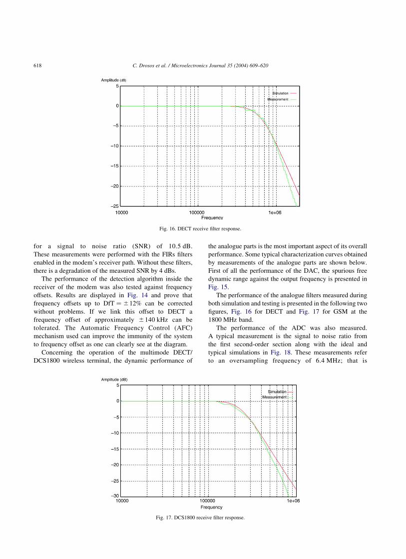
The performance of the analogue filters measured during
both simulation and testing is presented in the following two
figures, Fig. 16 for DECT and Fig. 17 for GSM at the
1800 MHz band.
The performance of the ADC was also measured.
A typical measurement is the signal to noise ratio from
the first second-order section along with the ideal and
typical simulations in Fig. 18. These measurements refer
to an oversampling frequency of 6.4 MHz; that is
Fig. 16. DECT receive filter response.
Fig. 17. DCS1800 receive filter response.
C. Drosos et al. / Microelectronics Journal 35 (2004) 609–620618
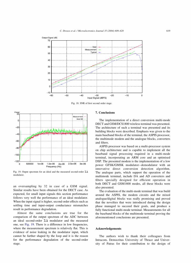
an oversampling by 32 in case of a GSM signal.
Similar results have been obtained for the DECT case. As
expected, for small input signals this section performance
follows very well the performance of an ideal modulator.
When the input signal is higher, second order effects such as
settling time and input-output conductance mismatches
result in performance degradation.
Almost the same conclusions are true for the
comparison of the output spectrum of the ADC between
an ideal second-order SD modulator and the measured
one, see Fig. 19. There is a difference in low frequencies,
where the measurement spectrum is relatively flat. This is
evidence of noise leaking in the modulator input, which
cannot be further shaped by the loop and it is the reason
for the performance degradation of the second-order
stage.
7. Conclusions
The implementation of a direct conversion multi-mode
DECT and GSM/DCS1800 wireless terminal was presented.
The architecture of such a terminal was presented and its
building blocks were described. Emphasis was given to the
main baseband blocks of the terminal, the ASPIS processor,
the multimode modem and the analogue blocks, converters
and filters.
ASPIS processor was based on a multi-processor system
on chip architecture and is capable to implement all the
baseband signal processing required in a multi-mode
terminal, incorporating an ARM core and an optimised
DSP. The presented modem is the implementation of a low
power GFSK/GMSK modulator–demodulator with an
innovative direct conversion detection algorithm.
The analogue parts, which support the operation of the
multimode terminal, include DA and AD converters and
filters specially designed for efficient operation in
both DECT and GSM1800 modes, all these blocks were
also presented.
The evaluation of the multi-mode terminal that was build
around the ASPIS, the modem circuits and the mixed
analogue/digital blocks was really promising and proved
that the novelties that were introduced during the design
phase managed to succeed their goals, and produce a
fully functional multi-mode terminal. Measurements for all
the baseband blocks of the multimode terminal proving the
aforementioned conclusions are presented.
Acknowledgements
The authors wish to thank their colleagues from
Intracom, Democritus University of Thrace and Univer-
sity of Patras for their contribution to the design of
Fig. 18. SNR of first second order stage.
Fig. 19. Ouput spectrum for an ideal and the measured second-order SD
modulator.
C. Drosos et al. / Microelectronics Journal 35 (2004) 609–620 619
the DECT/DCS1800 terminal. This work was partially
supported by the European Union under the projects ASPIS
#20287, LPGD #25256 and I-MODE #25702 in context of
ESPRIT IV.
References
[1] J. Phillips, G. Mac Namee, Personal Wireless Communication With
DECT and PWT, Artech House, ISBN 0-89006-872-0, 1998.
[2] G. Schultes, P. Kreuzgruber, A.L. Scholtz, DECT transceiver
architectures: superheterodyne or direct conversion?, in: Proceedings
of 43rd IEEE Vehicular Technology Conference, Secaucus, N.J., May
18–20, 1993, pp. 953–956.
[3] E. Metaxakis, A. Tzimas, G. Kalivas, A low complexity baseband
receiver for direct conversion DECT-based portable communication
systems, in: Proceedings of IEEE International Conference on
Universal Personal Communications (ICUPC), Florence, Italy,
October 5–9, 1998, pp. 45–49.
[4] A. Abidi, Direct-conversion radio transceivers for digital communi-
cations, IEEE Journal of Solid-State Circuits 30 (12) (1995),
pp. 1399–1410.
[5] J. Sevenhans, D. Haspeslagh, et al., An integrated Si bipolar
RF transceiver for a zero IF 900 MHz GSM digital mobile radio
single chip RF up and RF down converter of a hand portable phone,
in: Proceedings of IEEE International Solid-State Circuits Con-
ference, February 1994.
[6] http://www.inside-gsm.com/inside-gsm_home.html
[7] C. Drosos, C. Dre, S. Blionas, D. Soudris, A low power baseband
processor for a potable dual mode DECT/GSM terminal, IEICE
Transactions on Information and Systems E86-D (10) (2003)
1976–1986.
[8] S. Furber, ARM: System-on-Chip Architecture, Addison-Wesley,
Reading, MA, 2000.
[9] H. Karathanasis, C. Dre, D. Metafas, S. Blionas, Designing a single
chip DSP for DECT and GSM/DCS-1800 baseband processing, Real
Time Magazine 3/96 (1996) 22–31.
[10] F. Ieromnimon, C. Dre, et al., On the integration of diverse testing
strategies in a low-power processor, in: Proceedings of Design
Automation and Test in Europe (DATE), Paris, France, March 2000.
[11] C. Muller-Schloer, F. Geerinckx, B. Stanford-Smith, R. Van Riet,
Embedded Microprocessor Systems, IOS Press, 1996, ISBN
90-5199-300-5.
[12] D. Soudris, M. Perakis, et al., Low-power design of a multi-mode
transceiver, in: Proceedings of International Symposium on Circuits
and Systems, ISCAS 2000, May 28–31, 2000, Geneva, Switzerland,
pp. II-721–724.
[13] J.M. Rabaey, Low Power Design Methodologies, Kluwer Academic,
1995, ISBN 0-7923-9630-8.
[14] N.D. Zervas, M. Perakis, D. Soudris, E. Metaxakis, A. Tzimas, G.
Kalivas, C.E. Goutis, Low-power design of a digital baseband
receiver for direct conversion DECT systems, IEEE Transactions on
Circuits and Systems-Part-II: Analog and Digital Signal Processing 48
(12) (2001) 1121–1131.
[15] K. Masselos, P. Merakos, T. Stouraitis, C.E. Goutis, A novel
methodology for power consumption reduction in a class of DSP
algorithms, in: Proceedings of IEEE International Symposium on
Circuits and Systems (ISCAS), Monterey, California, May–June
1998, pp. 199–202.
[16] C. Papadimitriou, K. Steiglitz, Combinatorial Optimization: Algor-
ithms and Complexity, Prentice Hall, New Jersey, 1982, ISBN 0-
13-152462-3.
[17] N. Zervas, D. Soudris, S. Theoharis, C.E. Goutis, A. Thanailakis,
A methodology for the behavioral-level event-driven power manage-
ment of digital receivers, in: Proceedings of IEEE International
Symposium on Circuits and Systems (ISCAS) 2000, May 28–31,
Geneva, Switzerland, pp. II-589–II-592.
[18] L. Benini, G. Micheli, Dynamic Power Management, Design
Techniques and CAD Tools, Kluwer Academic, 1997, ISBN
0-7923-8086-X.
[19] AMS: Austria Mikro Systeme, http://www.ams.co.at
[20] S. Bouras, T. Georgantas, et al., Current mode baseband interface for
communication applications, in: Proceedings of IEEE International
Conference on Electronics, Circuits, and Systems (ICECS), Pafos,
Cyprus, 5–8 September, 1999, pp. 533–536
[21] T. Georgantas1, S. Bouras, D. Dervenis, Y. Papananos, A comparison
between integrated current and voltage mode filters for baseband
applications, in: Proceedings of IEEE International Conference on
Electronics, Circuits, and Systems (ICECS), Pafos, Cyprus, 5–8
September, 1999, pp. 485–488.
[22] F. Medeiro, et al., Fourth-order cascade SC SD modulators: a
comparative study, IEEE Transactions on Circuits Systems I 45
(1998) 1041–1051.
[23] T. Georgantas, S. Bouras, et al., Switched-current SD modulator for
baseband channel applications, in: Proceedings of IEEE International
Symposium on Circuits and Systems (ISCAS), Geneva, Switzerland,
28–31 May 2000, pp. IV-413–416.
C. Drosos et al. / Microelectronics Journal 35 (2004) 609–620620