the design of an asynchronous risc processor by pee
TRANSCRIPT
The Design of An Asynchronous RISC Processor
Bachelor of Information Technology (Honours) Computer Engineering
Faculty of Information and Communication Technology (Kampar Campus), UTAR
The Design of An Asynchronous RISC Processor
BY
PEE YAO HONG
A REPORT
SUBMITTED TO
Universiti Tunku Abdul Rahman
in partial fulfillment of the requirements
for the degree of
BACHELOR OF INFORMATION TECHNOLOGY
(HONOURS) COMPUTER ENGINEERING
Faculty of Information and Communication Technology
(Kampar Campus)
JAN 2021
The Design of An Asynchronous RISC Processor
Bachelor of Information Technology (Honours) Computer Engineering
Faculty of Information and Communication Technology (Kampar Campus), UTAR
UNIVERSITI TUNKU ABDUL RAHMAN
REPORT STATUS DECLARATION FORM
Title: __________________________________________________________
__________________________________________________________
__________________________________________________________
Academic Session: _____________
I __________________________________________________________
(CAPITAL LETTER)
declare that I allow this Final Year Project Report to be kept in
Universiti Tunku Abdul Rahman Library subject to the regulations as follows:
1. The dissertation is a property of the Library.
2. The Library is allowed to make copies of this dissertation for academic purposes.
Verified by,
_________________________ _________________________
(Author’s signature) (Supervisor’s signature)
Address:
__________________________
__________________________ _________________________
__________________________ Supervisor’s name
Date: _____________________ Date: ____________________
The Design of An Asynchronous RISC Processor
2021/01
PEE YAO HONG
K-90L, TAMAN IDAMAN,
MOK KAI MING JALAN JAKAR, 24000
KEMAMAN, TERENGGANU
16/04/2021 16/04/2021
The Design of An Asynchronous RISC Processor
i
Bachelor of Information Technology (Honours) Computer Engineering
Faculty of Information and Communication Technology (Kampar Campus), UTAR
The Design of An Asynchronous RISC Processor
BY
PEE YAO HONG
A REPORT
SUBMITTED TO
Universiti Tunku Abdul Rahman
in partial fulfillment of the requirements
for the degree of
BACHELOR OF INFORMATION TECHNOLOGY
(HONOURS) COMPUTER ENGINEERING
Faculty of Information and Communication Technology
(Kampar Campus)
JAN 2021
The Design of An Asynchronous RISC Processor
ii
Bachelor of Information Technology (Honours) Computer Engineering
Faculty of Information and Communication Technology (Kampar Campus), UTAR
DECLARATION OF ORIGINALITY
I declare that this report entitled “The Design of An Asynchronous RISC
Processor” is my own work except as cited in the references. The report has not been
accepted for any degree and is not being submitted concurrently in candidature for
any degree or other award.
Signature :
Name : PEE YAO HONG
Date : 16/04/2021

The Design of An Asynchronous RISC Processor
iii
Bachelor of Information Technology (Honours) Computer Engineering
Faculty of Information and Communication Technology (Kampar Campus), UTAR
ACKNOWLEDGEMENTS
I would like to express my sincere thanks and appreciation to my supervisors, Mr
Mok Kai Ming who has given me this bright opportunity to engage in a digital system
design project. It is my first step to establish a career in digital system design field. A
million thanks to you.
A million thanks to my family, especially my parents, for their patience,
unconditional support and love, and for always backing me up throughout the course.
They have always been there to provide me with financial support.
To my course mates of CT course, I would like to txtend my gratitude for their
friendship, company and encouragement during the course of my bachelor degree. We
had been putting in a lot of hard work together as a team for the past 3 years.
Finally, I would like to extend my sincere thanks to my seniors who have willingly
helped me out with their abilities, providing necessary and useful information about
the project. All the advises and suggestions had contributed to the completion of this
project.
The Design of An Asynchronous RISC Processor
iv
Bachelor of Information Technology (Honours) Computer Engineering
Faculty of Information and Communication Technology (Kampar Campus), UTAR
Abstract
This project is an asynchronous processor design project for academic purpose. It
will provide students with the methodology, concept and design of asynchronous
RISC processor. This will be illustrated by converting a synchronous processor to an
asynchronous processor. This can be done by substituting the global clock for a
synchronous processor with a set of controllers that all have an equivalent behavior.
Since asynchronous processor is better than synchronous processor in aspects of no
clock skew, lower power dissipation and etc, it is well suited for digital circuits and
therefore implemented in this project. The tools used in this project are Verilog
hardware description language in combination with ModelSim synthesis tools and
PCSpim. Moreover, there is several types of asynchronous implementation style and
the one used here is the 4-phase single-rail pipeline. The verification plan of the
project is a testbench with numbers of instruction to make sure the processor is
workable. Lastly, the output of the project would be the synthesized hardware of
asynchronous RISC processor with shortest delay for every single instruction in order
to implement that asynchronous processor is better than synchronous processor.
The Design of An Asynchronous RISC Processor
v
Bachelor of Information Technology (Honours) Computer Engineering
Faculty of Information and Communication Technology (Kampar Campus), UTAR
Table of Contents
TITLE PAGE i
DECLARATION OF ORIGINALITY ii
ACKNOWLEDGEMENTS iii
ABSTRACT iv
TABLE OF CONTENTS v - vii
LIST OF TABLES viii
LIST OF FIGURES ix - x
LIST OF ABBREVIATIONS xi
CHAPTER 1 : INTRODUCTION
1.1 Problem Statement and Motivation 1 - 4
1.2 Project Scope 5
1.3 Problem Objectives 5
1.4 Impact, Significance and Contribution 6
1.5 Background Information 7
CHAPTER 2 : LITERATURE REVIEW
2.1 Literature Review 8 - 15
2.2 Data Collection 16
2.3 Critical Remark of Previous Works 17
CHAPTER 3 : HARDWARE DEVELOPMENT
3.1 System Overview 18
3.1.1 Design Hierarchy 18 - 19
3.1.2 Internal Operation 20
3.1.3 Memory Map 21
3.2 CPU 22
3.2.1 Pipeline Micro-architecture 22 - 23
3.3 Design Block Specification 24
3.3.1 Main Control Block 24 - 28
The Design of An Asynchronous RISC Processor
vi
Bachelor of Information Technology (Honours) Computer Engineering
Faculty of Information and Communication Technology (Kampar Campus), UTAR
3.3.2 Arithmetic Logic Control Block 28
3.3.3 Register File Block 29 - 31
3.3.4 Forwarding Block 32 - 37
3.3.5 Interlock Block 38 - 39
3.3.6 ALU Block 40 - 41
3.3.7 Multiplier Block 42 - 43
3.3.8 Boot ROM Unit 43
3.3.9 Data and Stack RAM Unit 44 - 45
CHAPTER 4 : METHODLOGY AND TOOLS
4.1 Design Specifications 46
4.1.1 Methodologies and General Work Procedures 46 - 47
4.1.2 Development Tools 47 - 48
4.1.3 Verification Plan 48
4.2 Timeline 49
CHAPTER 5 : MULLER C-ELEMENT
5.1 Muller Pipeline 50
5.2 Circuit Implementation Style 52 - 55
5.3 Implementation of Pipeline 56
5.4 Micro-architecture of Asynchronous Processor 57
CHAPTER 6 : VERIFICATION
6.1 Simulation Result 58 - 60
CHAPTER 7 : SYNTHESIS 61
7.1 Utilization Report
CHAPTER 8 : CONCLUSION AND FUTURE WORK
8.1 Conclusion 62
8.2 Future Work 62
The Design of An Asynchronous RISC Processor
vii
Bachelor of Information Technology (Honours) Computer Engineering
Faculty of Information and Communication Technology (Kampar Campus), UTAR
BIBLIOGRAPHY 63
POSTER 64 – 65
PLAGIARISM CHECK RESULT 66 - 67
FYP2 CHECKLIST 68
The Design of An Asynchronous RISC Processor
viii
Bachelor of Information Technology (Honours) Computer Engineering
Faculty of Information and Communication Technology (Kampar Campus), UTAR
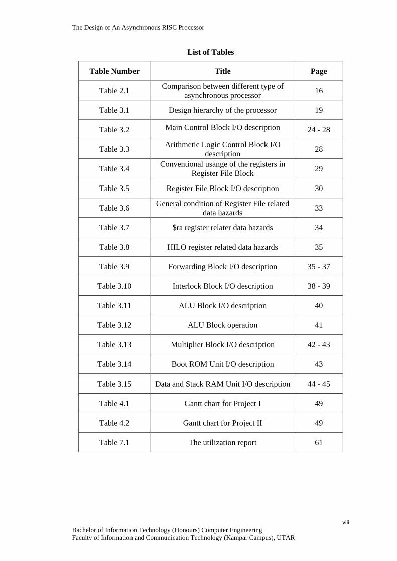
List of Tables
Table Number Title Page
Table 2.1 Comparison between different type of
asynchronous processor 16
Table 3.1 Design hierarchy of the processor 19
Table 3.2 Main Control Block I/O description 24 - 28
Table 3.3 Arithmetic Logic Control Block I/O
description 28
Table 3.4 Conventional usange of the registers in
Register File Block 29
Table 3.5 Register File Block I/O description 30
Table 3.6 General condition of Register File related
data hazards 33
Table 3.7 $ra register relater data hazards 34
Table 3.8 HILO register related data hazards 35
Table 3.9 Forwarding Block I/O description 35 - 37
Table 3.10 Interlock Block I/O description 38 - 39
Table 3.11 ALU Block I/O description 40
Table 3.12 ALU Block operation 41
Table 3.13 Multiplier Block I/O description 42 - 43
Table 3.14 Boot ROM Unit I/O description 43
Table 3.15 Data and Stack RAM Unit I/O description 44 - 45
Table 4.1 Gantt chart for Project I 49
Table 4.2 Gantt chart for Project II 49
Table 7.1 The utilization report 61
The Design of An Asynchronous RISC Processor
ix
Bachelor of Information Technology (Honours) Computer Engineering
Faculty of Information and Communication Technology (Kampar Campus), UTAR
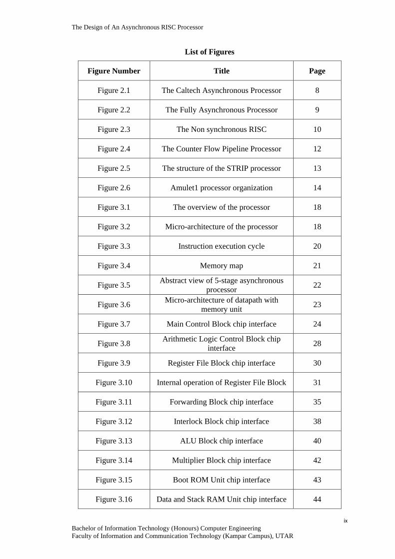
List of Figures
Figure Number Title Page
Figure 2.1 The Caltech Asynchronous Processor 8
Figure 2.2 The Fully Asynchronous Processor 9
Figure 2.3 The Non synchronous RISC 10
Figure 2.4 The Counter Flow Pipeline Processor 12
Figure 2.5 The structure of the STRIP processor 13
Figure 2.6 Amulet1 processor organization 14
Figure 3.1 The overview of the processor 18
Figure 3.2 Micro-architecture of the processor 18
Figure 3.3 Instruction execution cycle 20
Figure 3.4 Memory map 21
Figure 3.5 Abstract view of 5-stage asynchronous
processor 22
Figure 3.6 Micro-architecture of datapath with
memory unit 23
Figure 3.7 Main Control Block chip interface 24
Figure 3.8 Arithmetic Logic Control Block chip
interface 28
Figure 3.9 Register File Block chip interface 30
Figure 3.10 Internal operation of Register File Block 31
Figure 3.11 Forwarding Block chip interface 35
Figure 3.12 Interlock Block chip interface 38
Figure 3.13 ALU Block chip interface 40
Figure 3.14 Multiplier Block chip interface 42
Figure 3.15 Boot ROM Unit chip interface 43
Figure 3.16 Data and Stack RAM Unit chip interface 44
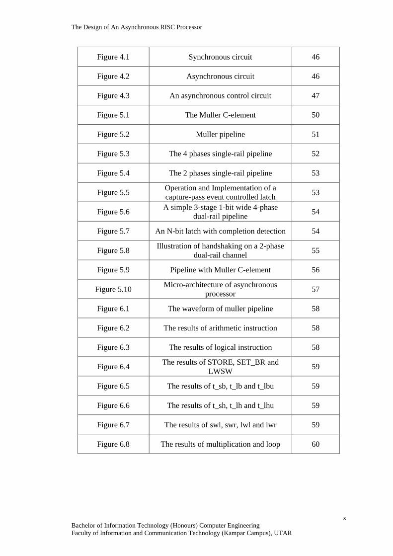
The Design of An Asynchronous RISC Processor
x
Bachelor of Information Technology (Honours) Computer Engineering
Faculty of Information and Communication Technology (Kampar Campus), UTAR
Figure 4.1 Synchronous circuit 46
Figure 4.2 Asynchronous circuit 46
Figure 4.3 An asynchronous control circuit 47
Figure 5.1 The Muller C-element 50
Figure 5.2 Muller pipeline 51
Figure 5.3 The 4 phases single-rail pipeline 52
Figure 5.4 The 2 phases single-rail pipeline 53
Figure 5.5 Operation and Implementation of a
capture-pass event controlled latch 53
Figure 5.6 A simple 3-stage 1-bit wide 4-phase
dual-rail pipeline 54
Figure 5.7 An N-bit latch with completion detection 54
Figure 5.8 Illustration of handshaking on a 2-phase
dual-rail channel 55
Figure 5.9 Pipeline with Muller C-element 56
Figure 5.10 Micro-architecture of asynchronous
processor 57
Figure 6.1 The waveform of muller pipeline 58
Figure 6.2 The results of arithmetic instruction 58
Figure 6.3 The results of logical instruction 58
Figure 6.4 The results of STORE, SET_BR and
LWSW 59
Figure 6.5 The results of t_sb, t_lb and t_lbu 59
Figure 6.6 The results of t_sh, t_lh and t_lhu 59
Figure 6.7 The results of swl, swr, lwl and lwr 59
Figure 6.8 The results of multiplication and loop 60
The Design of An Asynchronous RISC Processor
xi
Bachelor of Information Technology (Honours) Computer Engineering
Faculty of Information and Communication Technology (Kampar Campus), UTAR
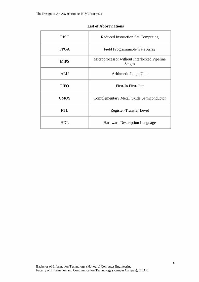
List of Abbreviations
RISC Reduced Instruction Set Computing
FPGA Field Programmable Gate Array
MIPS Microprocessor without Interlocked Pipeline
Stages
ALU Arithmetic Logic Unit
FIFO First-In First-Out
CMOS Complementary Metal Oxide Semiconductor
RTL Register-Transfer Level
HDL Hardware Description Language
The Design of An Asynchronous RISC Processor
1
Bachelor of Information Technology (Honours) Computer Engineering
Faculty of Information and Communication Technology (Kampar Campus), UTAR
Chapter 1 : Introduction
1.1 Problem statement and Motivation
A 32-bit five stage pipeline asynchronous RISC soft-core can be beneficial in
creating a core-based environment to support research and development work in the
area of developing IP cores. On the other hand, there are restrictions in obtaining such
workable core-based design environment as microprocessors are developed by
microchip design companies as IP for commercial purpose and most of these IP are
trade secret of those companies.
There are some asynchronous processor cores projects available freely online
such as www.opencore.org, www.ics.forth.gr/carv/aspida/ and etc. However, the
asynchronous processor’s micro-architecture included in these projects is not well
presented. Other than that, the Verilog codes wrote in these projects are also hard to
understand because of the confused naming convention used.
Furthermore, the verification plans for the asynchronous processor which
available on the open source are not completed. The lack of complete verification for
the processor will affect the process of design. Therefore, there is a necessary to
develop a verification plan to verify the functionality of the asynchronous processor.
Last but not least, the senior who took this FYP title previously was not able to
finish her work. The outputs of the supported insturctions are incorrect and the
synthesis of the asynchronous processor on FPGA has not been done yet.
The Design of An Asynchronous RISC Processor
2
Bachelor of Information Technology (Honours) Computer Engineering
Faculty of Information and Communication Technology (Kampar Campus), UTAR
Nowadays, there are a lot of digital system designed as synchronous. In
synchronous circuits, the data stored in memory devices named flip-flops. The
flip-flop output the data at discrete instants of time which specified by a clock signal
connected to it. This synchronous circuits built based on two assumptions which are
the signals are in binary and every parts share a same clock signal. (Jens Sparsø &
Steve 2001, p3)
By assuming all signals are in binary, the logic inside the circuit can be illustrated
by simple Boolean logic. Moreover, by assuming every parts share a same clock
signal, something happen inside the circuit can be ignored such as hazards and
feedback. However, when the complexity of system and speed of clock increase,
synchronous design has a lot of problems because of its way of keeping operations in
lock-step execution. The problems are stated below (Hans Jacobson 1996, p13-14):
⚫ Worst Case Performance
The clock frequency determines the speed of asynchronous circuit. The clock
signal should be big enough to run the worst-case delay and this is the reason
why synchronous circuit has worst case performance.
⚫ Clock Skew
Clock skew is defined as difference in arrival times of a clock signal at
different block or stage. All modules of the synchronous circuit need to
operate with a same clock in order to operate correctly. It is difficult to
minimize the clock skew with a large circuit.
⚫ Higher Power Consumption
As synchronous circuit is clocked by a global clock which include those
which are not use at a certain cycle. It toggles some of the node unnecessarily
and this causes higher power consumption. Other than that, switching of the
gate and fanout problem at the root of the clock tree also consume a lot of
power.
The Design of An Asynchronous RISC Processor
3
Bachelor of Information Technology (Honours) Computer Engineering
Faculty of Information and Communication Technology (Kampar Campus), UTAR
⚫ Easier Influenced by The Variations
Semiconductors mainly affected by process speed of fabrication, power
supply voltage level and temperature. These three properties will cause a
transistor to operate faster or slower. Synchronous circuit need to consider
these physical properties across its entire range in order to ensure the device
is functioning.
⚫ Worse Modularity and Composability
Synchronous designer always take serious consideration on satify the
detailed interfacial timing specifications. Other than that, replacing new parts
do not give advantage to synchronous circuit because one of the part changes,
the clock frequency of the whole circuit also need to be changed either
follows the old clock frequency or adjust other parts to suit the new clock
frequency.
Asynchronous circuits also assume all signals are in binary but there is no same
clock signal. Other than that, asynchronous circuits is self-timed instead of governed
by a block clock signal. The components inside the circuits use handshaking between
each other in order to communicate. A particular component only clocked when it is
needed.
Unlike synchronous circuits, asynchronous circuits do not suffer from the
problems stated above but it has a lot of advantages which stated below (Jens Sparsø
& Steve 2001, p3-4):
⚫ Averange Case Performance
Asynchronous circuit is controlled by local communications which will
direct initial the next computation when the other one is completed. When
the computation completed early, the new one can start early and this is why
asynchronous circuit does not exhibit worse case perfromance but an
averange case performance.
The Design of An Asynchronous RISC Processor
4
Bachelor of Information Technology (Honours) Computer Engineering
Faculty of Information and Communication Technology (Kampar Campus), UTAR
⚫ No Clock Skew
Asynchronous circuit is built up with small self-timed circuit which means
there is no global clock signal connected between each other. So, there is no
need to worry about the clock skew.
⚫ Lower Power Consumption
Asynchronous circuit only toggles the block or stage when it is being used,
thus reduring the power consumption.
⚫ Robustness Towards Variations
The self-timed logic and processing logic in asynchronous circuit are located
in the same area, both of them are affected by the same environmental
changes so that it is more unaffected to transient changes.
⚫ Better Modularity and Composability
Asynchronous circuist is simply connect a proper module with a matching
interfacial specifications which means sequences of events that take place but
not include the timing of the event. It saves a lot of time when designing the
asynchronous circuit because of no need to worry about the delays occur
inside the individual module. Other than that, parts of the asynchronous
circuit can be replaced by the new one in order to improve the performance.
The Design of An Asynchronous RISC Processor
5
Bachelor of Information Technology (Honours) Computer Engineering
Faculty of Information and Communication Technology (Kampar Campus), UTAR
1.2 Project Scope
There is an enorous field of research which covers widely diverse techniques to
the implementation of asynchronous design. However, this project will only focus on
the goals listed below:
⚫ Architecture of the asynchronous processor.
⚫ Methodologies used to implement the asynchronous processor.
1.3 Project Objectives
The main objective of this project is to design and synthesis the asynchronous
RISC processor, and it still can be divided into several sub-objectives as stated below:
⚫ Design Level
- To design and develop an asynchronous RISC processor that can meet all
the specifications correctly by using Verilog HDL.
⚫ Verification Level
- To develop a complete testbench to verify all the functional correctness of
the asynchronous RISC processor.
⚫ Synthesis Level
- To synthesis and integrate the asynchronous RISC processor which is the
FPGA technology.
The Design of An Asynchronous RISC Processor
6
Bachelor of Information Technology (Honours) Computer Engineering
Faculty of Information and Communication Technology (Kampar Campus), UTAR
1.4 Impact, significance and contribution
As a summary to the problem statement, there is a lack of well-developed and
well-founded 32-bit asynchronous RISC processor core-based development
environment. The development environment refers to the availability of the following:
• A well-developed design document, which includes the chip specification,
architecture specification and micro-architecture specification.
• A fully functional well-developed 32-bit asynchronous RISC architecture
core in the form of synthesis-ready RTL written in Verilog HDL.
• A well-developed verification environment for the 32-bit asynchronous RISC
core. The verification specification should contain suitable verification
methodology, verification techniques, test plans, test bench architectures etc.
• A complete physical design in Field Programmable Gate Array (FPGA) with
documented timing and resource usage information.
With the available well-developed basic 32-bit asynchronous RISC RTL model
(which has been fully functional verified), the verification environment and the design
documents, researchers can develop their own specific RTL model as part of the
development environment (whether directly modifying the internals of the processor
or interface to the processor) and can quickly verify their model to obtain results,
without having to worry about the development of the verification environment and
the modeling environment. This can speed up the research work significantly. For
example, a researcher may have developed an image-processing algorithm and
modified the algorithm to obtain a structure that suits the hardware implementation.
The structure can be modeled in Verilog as part of a specialized data-path or as a
coprocessor interfacing to the asynchronous RISC processor.
The Design of An Asynchronous RISC Processor
7
Bachelor of Information Technology (Honours) Computer Engineering
Faculty of Information and Communication Technology (Kampar Campus), UTAR
1.5 Background information
A circuit is considered to be asynchronous if it does not employ a periodic clock
signal to synchronize its internal operations, an obvious example is asynchronous
processor. Unlike a conventional processor, the asynchronous processor does not
require a central clock to coordinate the progress of data through the pipeline. The
first asynchronous design came out on 1952 and are widely used in computer during
1960’s. However, during 1970’s, the interest of asynchronous design dropped and
disappeared after the appearance of synchronous design. The main reasons why was
this happened are because of the rapidly growing of complexity of digital systems and
the simplicity offered by synchronous design.
However, with the progress of time and the advance in technology, synchronous
design showed up several problems when higher performance was a need. The
problems include clock skew for high frequency systems, power consumption due to
increase of portability of digital systems and worst case performance. The
asynchronous design does not suffer from the problems. Therefore, attention of the
researchers and designers were created. Today, the semiconductor industry is giving
serious consideration to the adoption of asynchronous circuit technology. There are
some projects from the industry have proven that the design of asynchronous circuit is
achieve the significant benefits stated in (C.H. Van Berkel, M.B. Josephs & S.M.
Nowick 1999, p224-230).
The Design of An Asynchronous RISC Processor
8
Bachelor of Information Technology (Honours) Computer Engineering
Faculty of Information and Communication Technology (Kampar Campus), UTAR
Chapter 2 : Literature Review
2.1 Literature Review
There are several different asynchronous processors with their own architecture,
type of communication and data transfer protocol discussed by (Tony Werner &
Venkatesh Akella 1997, p.69-76) & (T.Samyuktha & K.Balachandra 2015,
p.10208-10211).
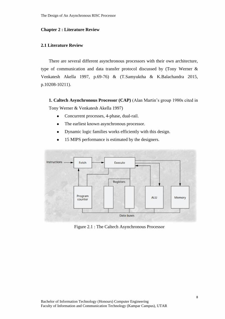
1. Caltech Asynchronous Processor (CAP) (Alan Martin’s group 1980s cited in
Tony Werner & Venkatesh Akella 1997)
⚫ Concurrent processes, 4-phase, dual-rail.
⚫ The earliest known asynchronous processor.
⚫ Dynamic logic families works efficiently with this design.
⚫ 15 MIPS performance is estimated by the designers.
Figure 2.1 : The Caltech Asynchronous Processor
The Design of An Asynchronous RISC Processor
9
Bachelor of Information Technology (Honours) Computer Engineering
Faculty of Information and Communication Technology (Kampar Campus), UTAR
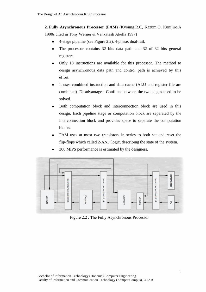
2. Fully Asynchronous Processor (FAM) (Kyoung.R.C, Kazum.O, Kunijiro.A
1990s cited in Tony Werner & Venkatesh Akella 1997)
⚫ 4-stage pipeline (see Figure 2.2), 4-phase, dual-rail.
⚫ The processor contains 32 bits data path and 32 of 32 bits general
registers.
⚫ Only 18 instructions are available for this processor. The method to
design asynchronous data path and control path is achieved by this
effort.
⚫ It uses combined instruction and data cache (ALU and register file are
combined). Disadvantage : Conflicts between the two stages need to be
solved.
⚫ Both computation block and interconnection block are used in this
design. Each pipeline stage or computation block are seperated by the
interconnection block and provides space to separate the computation
blocks.
⚫ FAM uses at most two transistors in series to both set and reset the
flip-flops which called 2-AND logic, describing the state of the system.
⚫ 300 MIPS performance is estimated by the designers.
Figure 2.2 : The Fully Asynchronous Processor
The Design of An Asynchronous RISC Processor
10
Bachelor of Information Technology (Honours) Computer Engineering
Faculty of Information and Communication Technology (Kampar Campus), UTAR
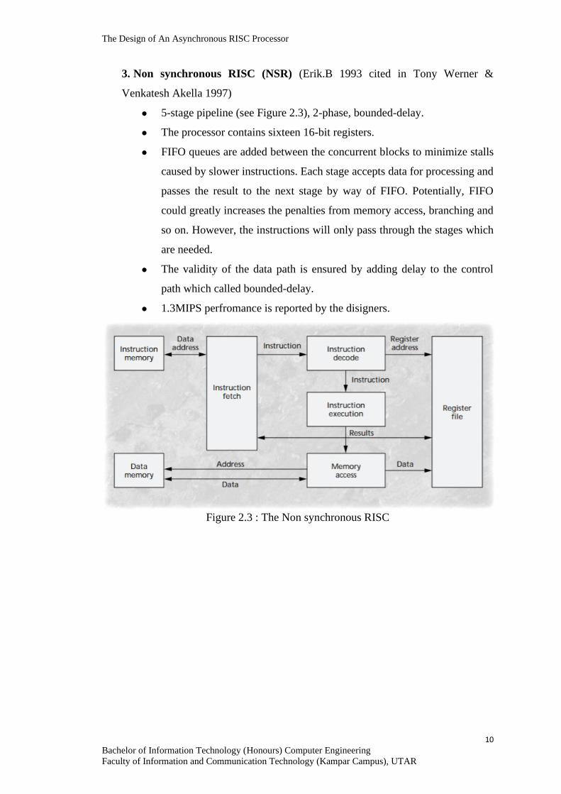
3. Non synchronous RISC (NSR) (Erik.B 1993 cited in Tony Werner &
Venkatesh Akella 1997)
⚫ 5-stage pipeline (see Figure 2.3), 2-phase, bounded-delay.
⚫ The processor contains sixteen 16-bit registers.
⚫ FIFO queues are added between the concurrent blocks to minimize stalls
caused by slower instructions. Each stage accepts data for processing and
passes the result to the next stage by way of FIFO. Potentially, FIFO
could greatly increases the penalties from memory access, branching and
so on. However, the instructions will only pass through the stages which
are needed.
⚫ The validity of the data path is ensured by adding delay to the control
path which called bounded-delay.
⚫ 1.3MIPS perfromance is reported by the disigners.
Figure 2.3 : The Non synchronous RISC
The Design of An Asynchronous RISC Processor
11
Bachelor of Information Technology (Honours) Computer Engineering
Faculty of Information and Communication Technology (Kampar Campus), UTAR
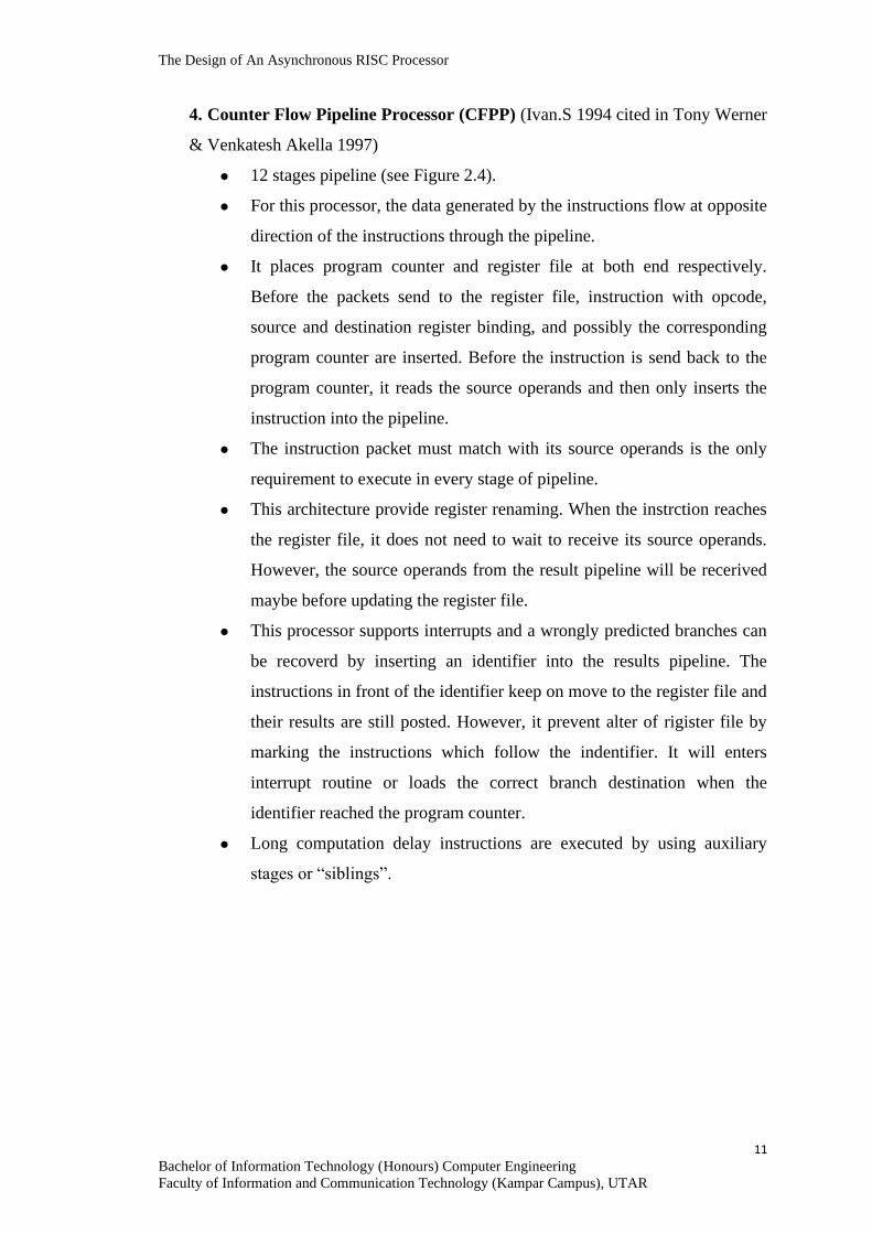
4. Counter Flow Pipeline Processor (CFPP) (Ivan.S 1994 cited in Tony Werner
& Venkatesh Akella 1997)
⚫ 12 stages pipeline (see Figure 2.4).
⚫ For this processor, the data generated by the instructions flow at opposite
direction of the instructions through the pipeline.
⚫ It places program counter and register file at both end respectively.
Before the packets send to the register file, instruction with opcode,
source and destination register binding, and possibly the corresponding
program counter are inserted. Before the instruction is send back to the
program counter, it reads the source operands and then only inserts the
instruction into the pipeline.
⚫ The instruction packet must match with its source operands is the only
requirement to execute in every stage of pipeline.
⚫ This architecture provide register renaming. When the instrction reaches
the register file, it does not need to wait to receive its source operands.
However, the source operands from the result pipeline will be recerived
maybe before updating the register file.
⚫ This processor supports interrupts and a wrongly predicted branches can
be recoverd by inserting an identifier into the results pipeline. The
instructions in front of the identifier keep on move to the register file and
their results are still posted. However, it prevent alter of rigister file by
marking the instructions which follow the indentifier. It will enters
interrupt routine or loads the correct branch destination when the
identifier reached the program counter.
⚫ Long computation delay instructions are executed by using auxiliary
stages or “siblings”.
The Design of An Asynchronous RISC Processor
12
Bachelor of Information Technology (Honours) Computer Engineering
Faculty of Information and Communication Technology (Kampar Campus), UTAR
Figure 2.4 : The Counter Flow Pipeline Processor
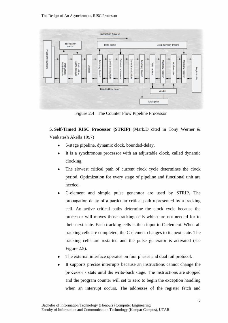
5. Self-Timed RISC Processor (STRIP) (Mark.D cited in Tony Werner &
Venkatesh Akella 1997)
⚫ 5-stage pipeline, dynamic clock, bounded-delay.
⚫ It is a synchronous processor with an adjustable clock, called dynamic
clocking.
⚫ The slowest critical path of current clock cycle determines the clock
period. Optimization for every stage of pipeline and functional unit are
needed.
⚫ C-element and simple pulse generator are used by STRIP. The
propagation delay of a particular critical path represented by a tracking
cell. An active critical paths determine the clock cycle because the
processor will moves those tracking cells which are not needed for to
their next state. Each tracking cells is then input to C-element. When all
tracking cells are completed, the C-element changes to its next state. The
tracking cells are restarted and the pulse generator is activated (see
Figure 2.5).
⚫ The external interface operates on four phases and dual rail protocol.
⚫ It supports precise interrupts because an instructions cannot change the
processor’s state until the write-back stage. The instructions are stopped
and the program counter will set to zero to begin the exception handling
when an interrupt occurs. The addresses of the register fetch and
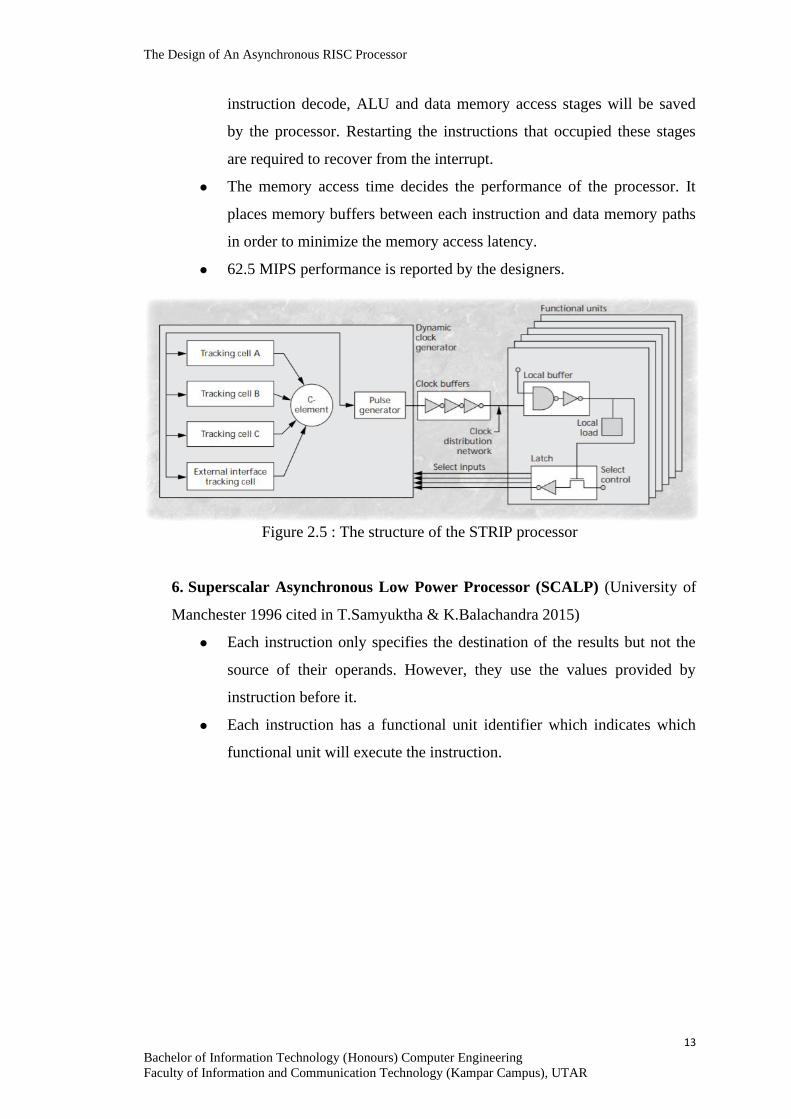
The Design of An Asynchronous RISC Processor
13
Bachelor of Information Technology (Honours) Computer Engineering
Faculty of Information and Communication Technology (Kampar Campus), UTAR
instruction decode, ALU and data memory access stages will be saved
by the processor. Restarting the instructions that occupied these stages
are required to recover from the interrupt.
⚫ The memory access time decides the performance of the processor. It
places memory buffers between each instruction and data memory paths
in order to minimize the memory access latency.
⚫ 62.5 MIPS performance is reported by the designers.
Figure 2.5 : The structure of the STRIP processor
6. Superscalar Asynchronous Low Power Processor (SCALP) (University of
Manchester 1996 cited in T.Samyuktha & K.Balachandra 2015)
⚫ Each instruction only specifies the destination of the results but not the
source of their operands. However, they use the values provided by
instruction before it.
⚫ Each instruction has a functional unit identifier which indicates which
functional unit will execute the instruction.
The Design of An Asynchronous RISC Processor
14
Bachelor of Information Technology (Honours) Computer Engineering
Faculty of Information and Communication Technology (Kampar Campus), UTAR
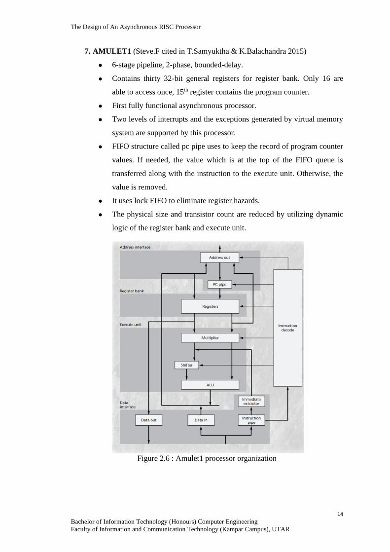
7. AMULET1 (Steve.F cited in T.Samyuktha & K.Balachandra 2015)
⚫ 6-stage pipeline, 2-phase, bounded-delay.
⚫ Contains thirty 32-bit general registers for register bank. Only 16 are
able to access once, 15th register contains the program counter.
⚫ First fully functional asynchronous processor.
⚫ Two levels of interrupts and the exceptions generated by virtual memory
system are supported by this processor.
⚫ FIFO structure called pc pipe uses to keep the record of program counter
values. If needed, the value which is at the top of the FIFO queue is
transferred along with the instruction to the execute unit. Otherwise, the
value is removed.
⚫ It uses lock FIFO to eliminate register hazards.
⚫ The physical size and transistor count are reduced by utilizing dynamic
logic of the register bank and execute unit.
Figure 2.6 : Amulet1 processor organization
The Design of An Asynchronous RISC Processor
15
Bachelor of Information Technology (Honours) Computer Engineering
Faculty of Information and Communication Technology (Kampar Campus), UTAR
8. AMULET2e - An Asynchronous Embedded Controller (Steve.F cited in
T.Samyuktha & K.Balachandra 2015)
⚫ It is designed as embedded system chip with an enhanced ARM core a
4Kbyte pipelined cache, a flexible memory interface and assorted
programmable control functions.
⚫ It also consists of counter-timer for real time reference.
⚫ AMULET2e silicon demonstrates competitive performance, power
efficiency and ease of design.
⚫ Pipeline reorganization was done with respect to AMULET1.
9. AMULET3 (Steve.F cited in T.Samyuktha & K.Balachandra 2015)
⚫ It is a fully asynchronous implementation of ARM architecture which
including 16 bit thumb instruction set.
⚫ Suitable for low power processor.
⚫ It is equal to a 32-bit embedded processor in energy efficiency and was
developed for microcontroller applications.
The Design of An Asynchronous RISC Processor
16
Bachelor of Information Technology (Honours) Computer Engineering
Faculty of Information and Communication Technology (Kampar Campus), UTAR
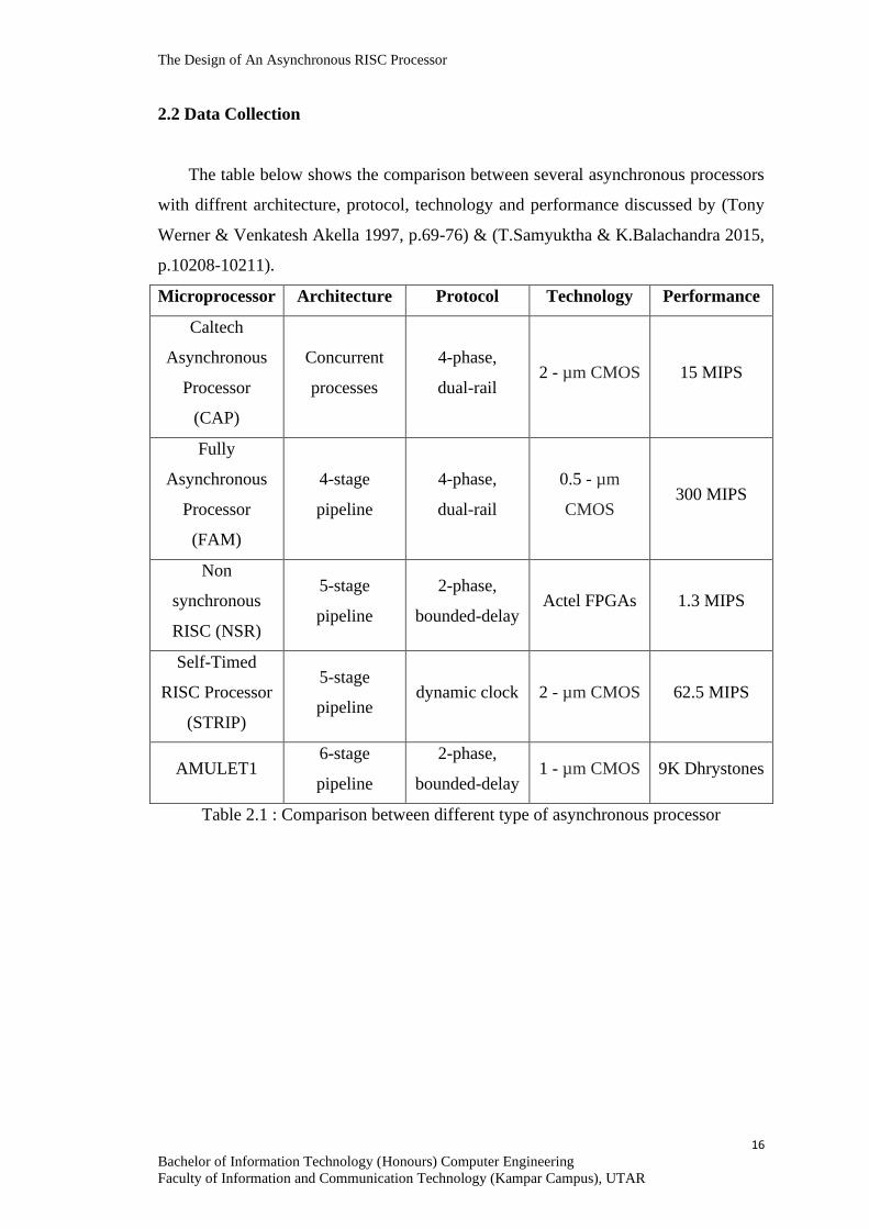
2.2 Data Collection
The table below shows the comparison between several asynchronous processors
with diffrent architecture, protocol, technology and performance discussed by (Tony
Werner & Venkatesh Akella 1997, p.69-76) & (T.Samyuktha & K.Balachandra 2015,
p.10208-10211).
Microprocessor Architecture Protocol Technology Performance
Caltech
Asynchronous
Processor
(CAP)
Concurrent
processes
4-phase,
dual-rail 2 - µm CMOS 15 MIPS
Fully
Asynchronous
Processor
(FAM)
4-stage
pipeline
4-phase,
dual-rail
0.5 - µm
CMOS 300 MIPS
Non
synchronous
RISC (NSR)
5-stage
pipeline
2-phase,
bounded-delay Actel FPGAs 1.3 MIPS
Self-Timed
RISC Processor
(STRIP)
5-stage
pipeline dynamic clock 2 - µm CMOS 62.5 MIPS
AMULET1 6-stage
pipeline
2-phase,
bounded-delay 1 - µm CMOS 9K Dhrystones
Table 2.1 : Comparison between different type of asynchronous processor
The Design of An Asynchronous RISC Processor
17
Bachelor of Information Technology (Honours) Computer Engineering
Faculty of Information and Communication Technology (Kampar Campus), UTAR
2.3 Critical Remarks of Previous Works
It can been seen that asynchronous circuits have more advantages than
synchronous circuits but it also have its own limitations. These limitations are stated
below ( Hans Jacobson 1996, p15-16):
⚫ Hazards. Asynchronous circuits are easily influenced by glitches and
hazards because it depend on the events within the wire to communicate.
Therefore, it is important to take care of it during state of synthesis in order
to remove the chance of function and logic hazards. Other than that, the
result of the circuit is also sensitive to glitches.
⚫ Latency with Handshake. The method where asynchronous circuits used to
communicate will slow down the performance due to handshake overhead.
The communicating elements are put close to each other in order to solve the
problem.
⚫ Different Design Methodologies. Inconsistent of specification and
implementation styles caused by different methodologies used to design the
asynchronous circuit. It is hard to compare the differences of those systems
and also difficult to pull off on exiting works.
⚫ Immature Synthesis Methodologies. There is a must for mature synthesis
methodologies in order to let asynchronous design to be accepted by those
synchronous designers and industry. Unfortunately, there are many methods
are still in their early stages of research. Other than that, it also has not yet
been modeled with real industrial designs.
The Design of An Asynchronous RISC Processor
18
Bachelor of Information Technology (Honours) Computer Engineering
Faculty of Information and Communication Technology (Kampar Campus), UTAR
Chapter 3 : Hardware Development
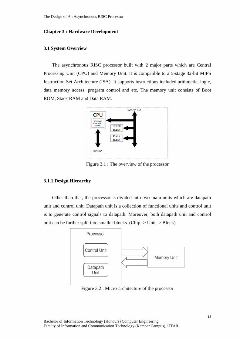
3.1 System Overview
The asynchronous RISC processor built with 2 major parts which are Central
Processing Unit (CPU) and Memory Unit. It is compatible to a 5-stage 32-bit MIPS
Instruction Set Architecture (ISA). It supports instructions included arithmetic, logic,
data memory access, program control and etc. The memory unit consists of Boot
ROM, Stack RAM and Data RAM.
Figure 3.1 : The overview of the processor
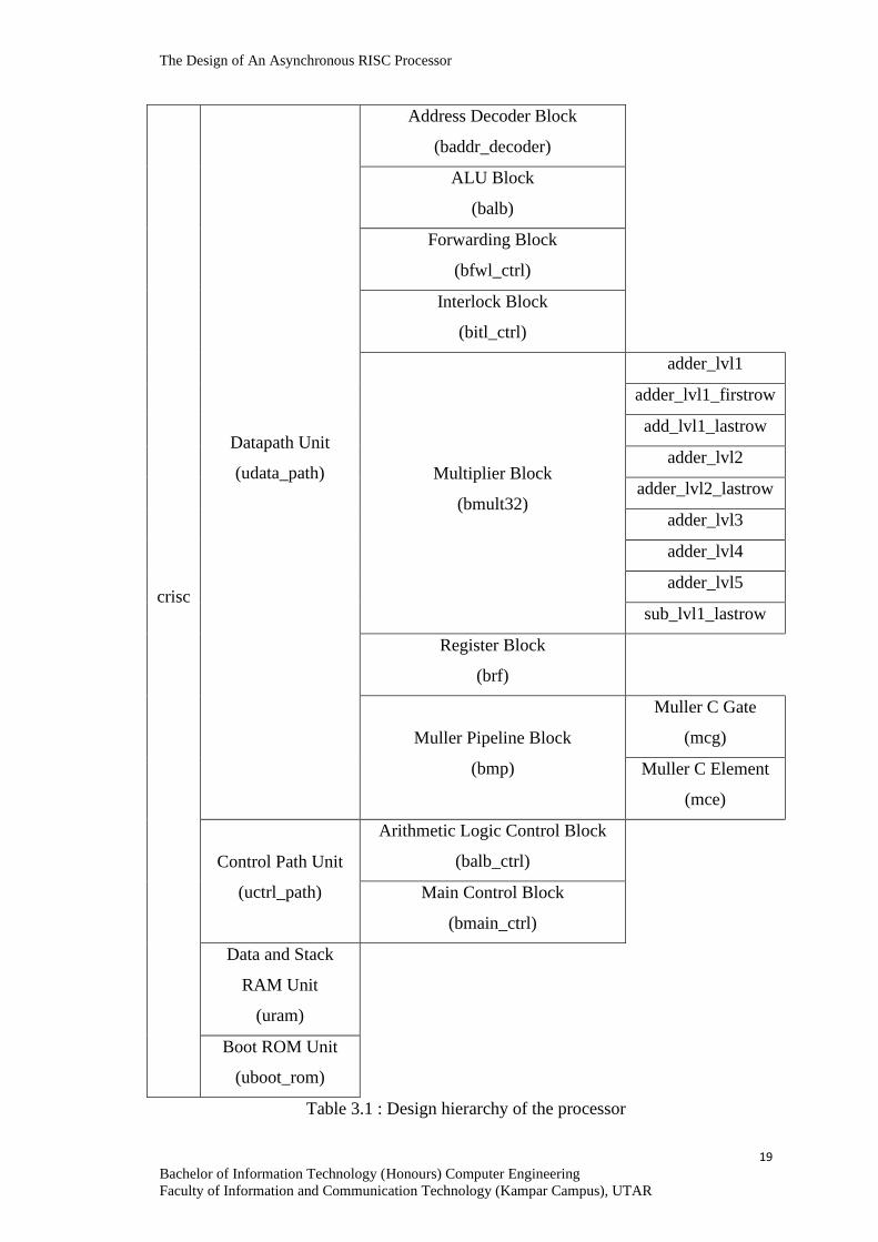
3.1.1 Design Hierarchy
Other than that, the processor is divided into two main units which are datapath
unit and control unit. Datapath unit is a collection of functional units and control unit
is to generate control signals to datapath. Moreover, both datapath unit and control
unit can be further split into smaller blocks. (Chip -> Unit -> Block)
Figure 3.2 : Micro-architecture of the processor
The Design of An Asynchronous RISC Processor
19
Bachelor of Information Technology (Honours) Computer Engineering
Faculty of Information and Communication Technology (Kampar Campus), UTAR
crisc
Datapath Unit
(udata_path)
Address Decoder Block
(baddr_decoder)
ALU Block
(balb)
Forwarding Block
(bfwl_ctrl)
Interlock Block
(bitl_ctrl)
Multiplier Block
(bmult32)
adder_lvl1
adder_lvl1_firstrow
add_lvl1_lastrow
adder_lvl2
adder_lvl2_lastrow
adder_lvl3
adder_lvl4
adder_lvl5
sub_lvl1_lastrow
Register Block
(brf)
Muller Pipeline Block
(bmp)
Muller C Gate
(mcg)
Muller C Element
(mce)
Control Path Unit
(uctrl_path)
Arithmetic Logic Control Block
(balb_ctrl)
Main Control Block
(bmain_ctrl)
Data and Stack
RAM Unit
(uram)
Boot ROM Unit
(uboot_rom)
Table 3.1 : Design hierarchy of the processor
The Design of An Asynchronous RISC Processor
20
Bachelor of Information Technology (Honours) Computer Engineering
Faculty of Information and Communication Technology (Kampar Campus), UTAR
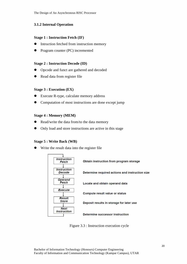
3.1.2 Internal Operation
Stage 1 : Instruction Fetch (IF)
⚫ Intruction fetched from instruction memory
⚫ Pragram counter (PC) incremented
Stage 2 : Instruction Decode (ID)
⚫ Opcode and funct are gathered and decoded
⚫ Read data from register file
Stage 3 : Execution (EX)
⚫ Execute R-type, calculate memory address
⚫ Computation of most instructions are done except jump
Stage 4 : Memory (MEM)
⚫ Read/write the data from/to the data memory
⚫ Only load and store instructions are active in this stage
Stage 5 : Write Back (WB)
⚫ Write the result data into the register file
Figure 3.3 : Instruction execution cycle
The Design of An Asynchronous RISC Processor
21
Bachelor of Information Technology (Honours) Computer Engineering
Faculty of Information and Communication Technology (Kampar Campus), UTAR
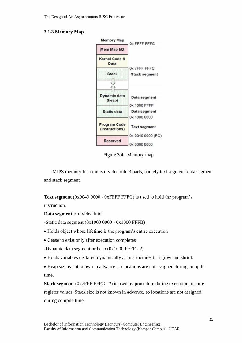
3.1.3 Memory Map
Figure 3.4 : Memory map
MIPS memory location is divided into 3 parts, namely text segment, data segment
and stack segment.
Text segment (0x0040 0000 - 0xFFFF FFFC) is used to hold the program’s
instruction.
Data segment is divided into:
-Static data segment (0x1000 0000 - 0x1000 FFFB)
• Holds object whose lifetime is the program’s entire execution
• Cease to exist only after execution completes
-Dynamic data segment or heap (0x1000 FFFF - ?)
• Holds variables declared dynamically as in structures that grow and shrink
• Heap size is not known in advance, so locations are not assigned during compile
time.
Stack segment (0x7FFF FFFC - ?) is used by procedure during execution to store
register values. Stack size is not known in advance, so locations are not assigned
during compile time
The Design of An Asynchronous RISC Processor
22
Bachelor of Information Technology (Honours) Computer Engineering
Faculty of Information and Communication Technology (Kampar Campus), UTAR
3.2 CPU
3.2.1 Pipeline Micro-architecture
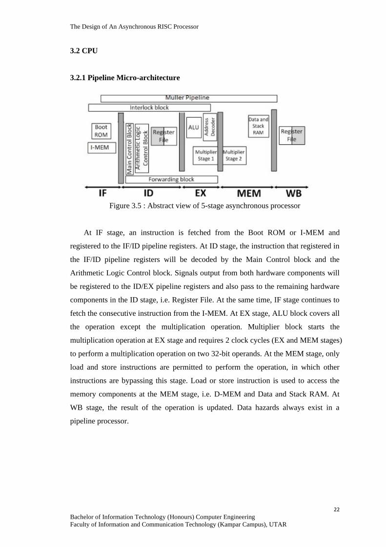
Figure 3.5 : Abstract view of 5-stage asynchronous processor
At IF stage, an instruction is fetched from the Boot ROM or I-MEM and
registered to the IF/ID pipeline registers. At ID stage, the instruction that registered in
the IF/ID pipeline registers will be decoded by the Main Control block and the
Arithmetic Logic Control block. Signals output from both hardware components will
be registered to the ID/EX pipeline registers and also pass to the remaining hardware
components in the ID stage, i.e. Register File. At the same time, IF stage continues to
fetch the consecutive instruction from the I-MEM. At EX stage, ALU block covers all
the operation except the multiplication operation. Multiplier block starts the
multiplication operation at EX stage and requires 2 clock cycles (EX and MEM stages)
to perform a multiplication operation on two 32-bit operands. At the MEM stage, only
load and store instructions are permitted to perform the operation, in which other
instructions are bypassing this stage. Load or store instruction is used to access the
memory components at the MEM stage, i.e. D-MEM and Data and Stack RAM. At
WB stage, the result of the operation is updated. Data hazards always exist in a
pipeline processor.
The Design of An Asynchronous RISC Processor
23
Bachelor of Information Technology (Honours) Computer Engineering
Faculty of Information and Communication Technology (Kampar Campus), UTAR
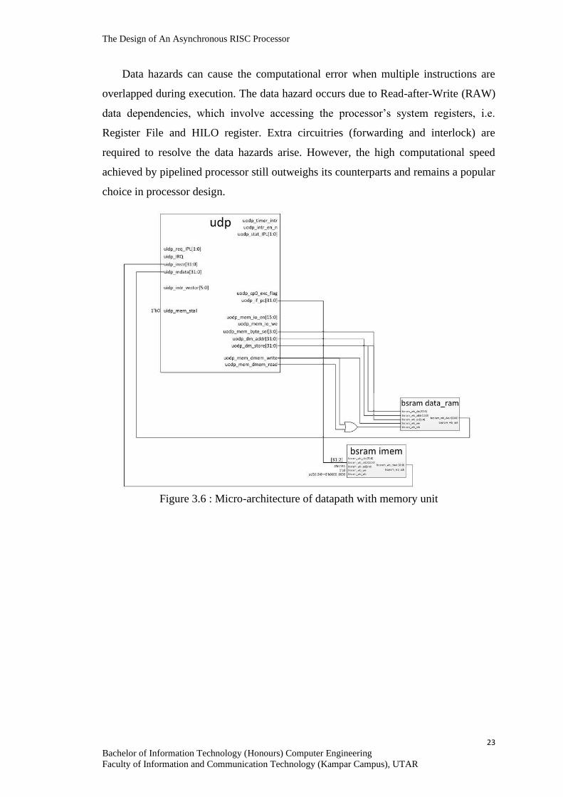
Data hazards can cause the computational error when multiple instructions are
overlapped during execution. The data hazard occurs due to Read-after-Write (RAW)
data dependencies, which involve accessing the processor’s system registers, i.e.
Register File and HILO register. Extra circuitries (forwarding and interlock) are
required to resolve the data hazards arise. However, the high computational speed
achieved by pipelined processor still outweighs its counterparts and remains a popular
choice in processor design.
Figure 3.6 : Micro-architecture of datapath with memory unit
The Design of An Asynchronous RISC Processor
24
Bachelor of Information Technology (Honours) Computer Engineering
Faculty of Information and Communication Technology (Kampar Campus), UTAR
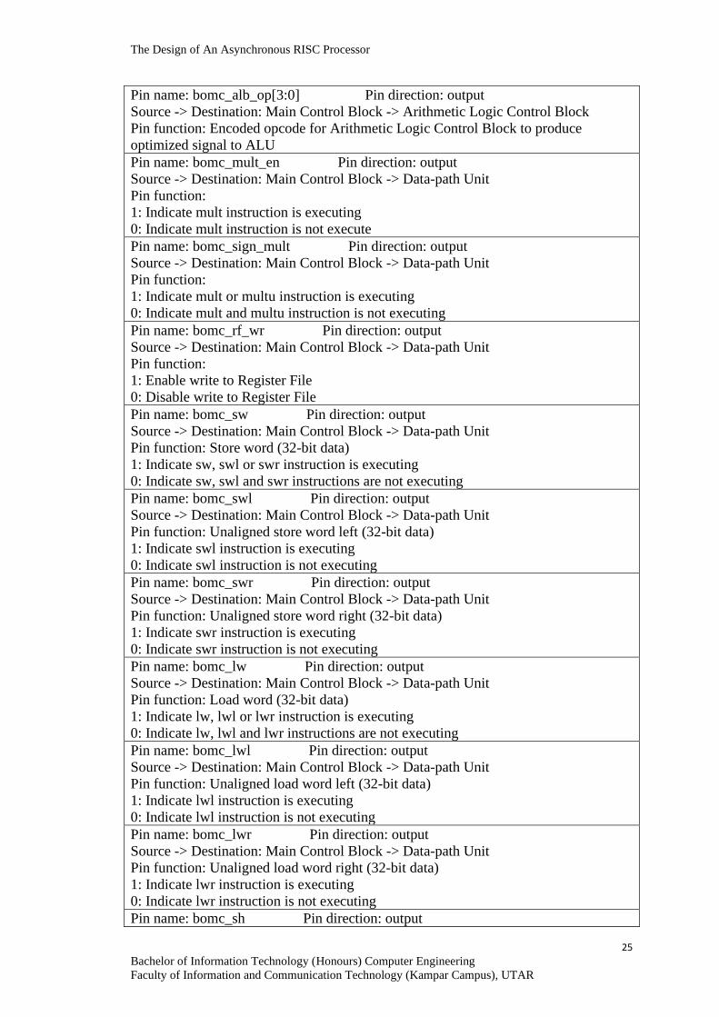
3.3 Design Block Specification
3.3.1 Main Control Block
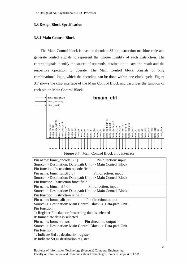
The Main Control block is used to decode a 32-bit instruction machine code and
generate control signals to represent the unique identity of each instruction. The
control signals identify the source of operands, destination to save the result and the
respective operation to operate. The Main Control block consists of only
combinational logic, which the decoding can be done within one clock cycle. Figure
3.7 shows the chip interface of the Main Control Block and describes the function of
each pin on Main Control Block.
Figure 3.7 : Main Control Block chip interface
Pin name: bimc_opcode[5:0] Pin direction: input
Source -> Destination: Data-path Unit -> Main Control Block
Pin function: Instruction opcode field
Pin name: bimc_funct[5:0] Pin direction: input
Source -> Destination: Data-path Unit -> Main Control Block
Pin function: Instruction funct field
Pin name: bimc_rs[4:0] Pin direction: input
Source -> Destination: Data-path Unit -> Main Control Block
Pin function: Instruction rs field
Pin name: bomc_alb_src Pin direction: output
Source -> Destination: Main Control Block -> Data-path Unit
Pin function:
1: Register File data or forwarding data is selected
0: Immediate data is selected
Pin name: bomc_rd_src Pin direction: output
Source -> Destination: Main Control Block -> Data-path Unit
Pin function:
1: Indicate $rd as destination register
0: Indicate $rt as destination register
The Design of An Asynchronous RISC Processor
25
Bachelor of Information Technology (Honours) Computer Engineering
Faculty of Information and Communication Technology (Kampar Campus), UTAR
Pin name: bomc_alb_op[3:0] Pin direction: output
Source -> Destination: Main Control Block -> Arithmetic Logic Control Block
Pin function: Encoded opcode for Arithmetic Logic Control Block to produce
optimized signal to ALU
Pin name: bomc_mult_en Pin direction: output
Source -> Destination: Main Control Block -> Data-path Unit
Pin function:
1: Indicate mult instruction is executing
0: Indicate mult instruction is not execute
Pin name: bomc_sign_mult Pin direction: output
Source -> Destination: Main Control Block -> Data-path Unit
Pin function:
1: Indicate mult or multu instruction is executing
0: Indicate mult and multu instruction is not executing
Pin name: bomc_rf_wr Pin direction: output
Source -> Destination: Main Control Block -> Data-path Unit
Pin function:
1: Enable write to Register File
0: Disable write to Register File
Pin name: bomc_sw Pin direction: output
Source -> Destination: Main Control Block -> Data-path Unit
Pin function: Store word (32-bit data)
1: Indicate sw, swl or swr instruction is executing
0: Indicate sw, swl and swr instructions are not executing
Pin name: bomc_swl Pin direction: output
Source -> Destination: Main Control Block -> Data-path Unit
Pin function: Unaligned store word left (32-bit data)
1: Indicate swl instruction is executing
0: Indicate swl instruction is not executing
Pin name: bomc_swr Pin direction: output
Source -> Destination: Main Control Block -> Data-path Unit
Pin function: Unaligned store word right (32-bit data)
1: Indicate swr instruction is executing
0: Indicate swr instruction is not executing
Pin name: bomc_lw Pin direction: output
Source -> Destination: Main Control Block -> Data-path Unit
Pin function: Load word (32-bit data)
1: Indicate lw, lwl or lwr instruction is executing
0: Indicate lw, lwl and lwr instructions are not executing
Pin name: bomc_lwl Pin direction: output
Source -> Destination: Main Control Block -> Data-path Unit
Pin function: Unaligned load word left (32-bit data)
1: Indicate lwl instruction is executing
0: Indicate lwl instruction is not executing
Pin name: bomc_lwr Pin direction: output
Source -> Destination: Main Control Block -> Data-path Unit
Pin function: Unaligned load word right (32-bit data)
1: Indicate lwr instruction is executing
0: Indicate lwr instruction is not executing
Pin name: bomc_sh Pin direction: output
The Design of An Asynchronous RISC Processor
26
Bachelor of Information Technology (Honours) Computer Engineering
Faculty of Information and Communication Technology (Kampar Campus), UTAR
Source -> Destination: Main Control Block -> Data-path Unit
Pin function: Store half-word (16-bit data)
1: Indicate sh instruction is executing
0: Indicate sh instruction is not executing
Pin name: bomc_sh Pin direction: output
Source -> Destination: Main Control Block -> Data-path Unit
Pin function: Store half-word (16-bit data)
1: Indicate sh instruction is executing
0: Indicate sh instruction is not executing
Pin name: bomc_lhu Pin direction: output
Source -> Destination: Main Control Block -> Data-path Unit
Pin function: Load half-word unsigned (16-bit data)
1: Indicate lhu instruction is executing
0: Indicate lhu instruction is not executing
Pin name: bomc_sb Pin direction: output
Source -> Destination: Main Control Block -> Data-path Unit
Pin function: Store byte (8-bit data)
1: Indicate sb instruction is executing
0: Indicate sb instruction is not executing
Pin name: bomc_lb Pin direction: output
Source -> Destination: Main Control Block -> Data-path Unit
Pin function: Load byte (8-bit data), sign extend required (refer uipr_load_sign_ext)
1: Indicate lb instruction is executing
0: Indicate lb instruction is not executing
Pin name: bomc_lbu Pin direction: output
Source -> Destination: Main Control Block -> Data-path Unit
Pin function: Load byte unsigned (8-bit data)
1: Indicate lbu instruction is executing
0: Indicate lbu instruction is not executing
Pin name: bomc_load_sign_ext Pin direction: output
Source -> Destination: Main Control Block -> Data-path Unit
Pin function:
1: Indicate lh or lb instruction is executing, sign extend 16-bit to lh or 24-bit to lb
0: Indicate lh or lb instructions are not executing
Pin name: bomc_sign_ext Pin direction: output
Source -> Destination: Main Control Block -> Data-path Unit
Pin function:
1: Immediate data sign extend
0: Immediate data zero extend
Pin name: bomc_mem_to_rf Pin direction: output
Source -> Destination: Main Control Block -> Data-path Unit
Pin function:
1: Data memory data to Register File
0: ALU block result to Register File
Pin name: bomc_alb_to_rf Pin direction: output
Source -> Destination: Main Control Block -> Data-path Unit
Pin function: Reserved for future development
Pin name: bomc_hi_to_rf Pin direction: output
Source -> Destination: Main Control Block -> Data-path Unit
Pin function:
The Design of An Asynchronous RISC Processor
27
Bachelor of Information Technology (Honours) Computer Engineering
Faculty of Information and Communication Technology (Kampar Campus), UTAR
1: HI register data to Register File
0: LO register data to Register File
Pin name: bomc_hilo_acc Pin direction: output
Source -> Destination: Main Control Block -> Data-path Unit
Pin function:
1: Indicate mflo or mfhi instruction is executing
0: Indicate mflo and mfhi instructions are not executing
Pin name: bomc_jump Pin direction: output
Source -> Destination: Main Control Block -> Data-path Unit
Pin function:
1: Indicate j instruction is executing
0: Indicate j instruction is not executing
Pin name: bomc_jr Pin direction: output
Source -> Destination: Main Control Block -> Data-path Unit
Pin function:
1: Indicate jr instruction is executing
0: Indicate jr instruction is not executing
Pin name: bomc_jal Pin direction: output
Source -> Destination: Main Control Block -> Data-path Unit
Pin function:
1: Indicate jal instruction is executing
0: Indicate jal instruction is not executing
Pin name: bomc_jalr Pin direction: output
Source -> Destination: Main Control Block -> Data-path Unit
Pin function:
1: Indicate jalr instruction is executing
0: Indicate jalr instruction is not executing
Pin name: bomc_beq Pin direction: output
Source -> Destination: Main Control Block -> Data-path Unit
Pin function:
1: Indicate beq instruction is executing
0: Indicate beq instruction is not executing
Pin name: bomc_bne Pin direction: output
Source -> Destination: Main Control Block -> Data-path Unit
Pin function:
1: Indicate bne instruction is executing
0: Indicate bne instruction is not executing
Pin name: bomc_blez Pin direction: output
Source -> Destination: Main Control Block -> Data-path Unit
Pin function:
1: Indicate blez instruction is executing
0: Indicate blez instruction is not executing
Pin name: bomc_bgtz Pin direction: output
Source -> Destination: Main Control Block -> Data-path Unit
Pin function:
1: Indicate bgtz instruction is executing
0: Indicate bgtz instruction is not executing
Pin name: bomc_lui Pin direction: output
Source -> Destination: Main Control Block -> Data-path Unit
Pin function:
The Design of An Asynchronous RISC Processor
28
Bachelor of Information Technology (Honours) Computer Engineering
Faculty of Information and Communication Technology (Kampar Campus), UTAR
1: Indicate lui instruction is executing
0: Indicate lui instruction is not executing
Pin name: bomc_rtype Pin direction: output
Source -> Destination: Main Control Block -> Data-path Unit
Pin function:
1: Indicate R-type instruction is executing
0: Indicate I-type or J-type instruction is executing
Table 3.2 : Main Control Block I/O description
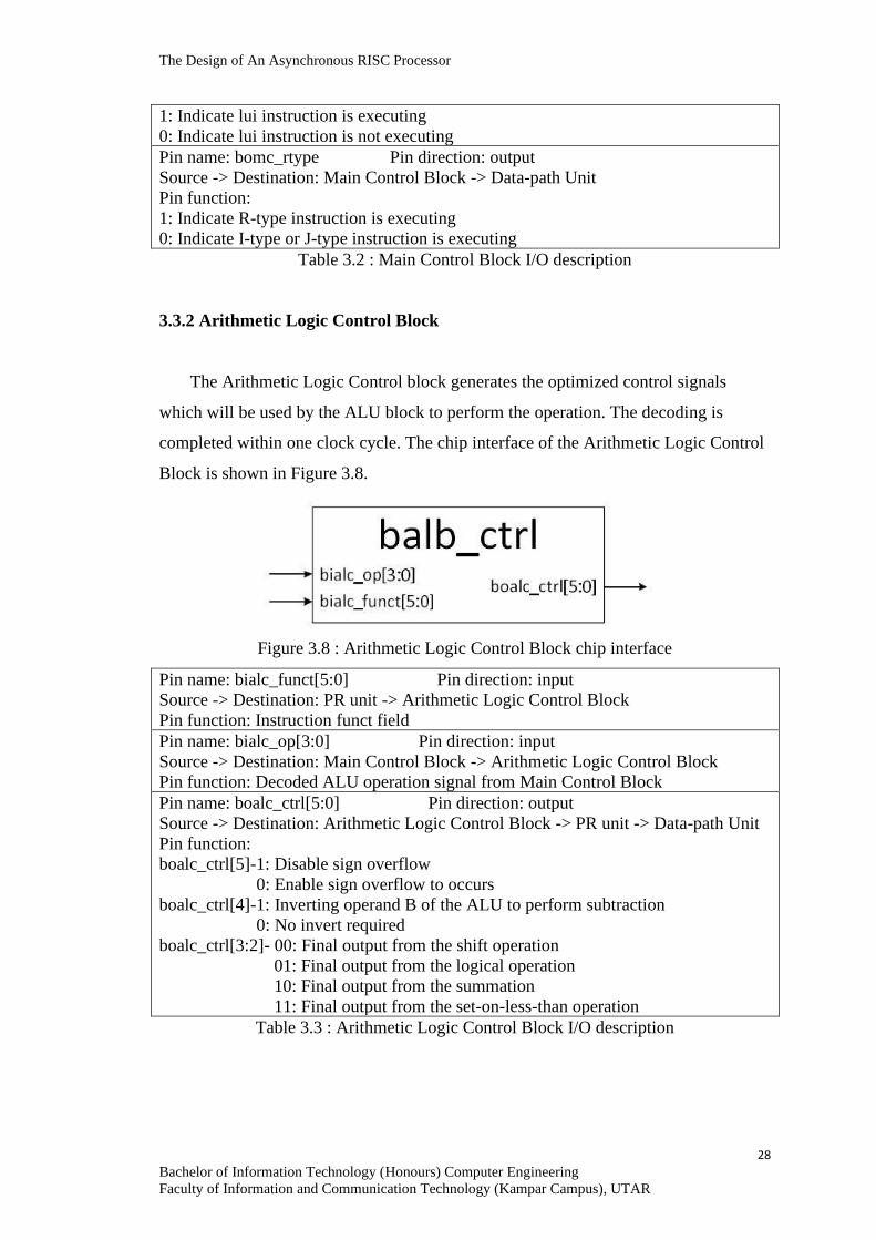
3.3.2 Arithmetic Logic Control Block
The Arithmetic Logic Control block generates the optimized control signals
which will be used by the ALU block to perform the operation. The decoding is
completed within one clock cycle. The chip interface of the Arithmetic Logic Control
Block is shown in Figure 3.8.
Figure 3.8 : Arithmetic Logic Control Block chip interface
Pin name: bialc_funct[5:0] Pin direction: input
Source -> Destination: PR unit -> Arithmetic Logic Control Block
Pin function: Instruction funct field
Pin name: bialc_op[3:0] Pin direction: input
Source -> Destination: Main Control Block -> Arithmetic Logic Control Block
Pin function: Decoded ALU operation signal from Main Control Block
Pin name: boalc_ctrl[5:0] Pin direction: output
Source -> Destination: Arithmetic Logic Control Block -> PR unit -> Data-path Unit
Pin function:
boalc_ctrl[5]-1: Disable sign overflow
0: Enable sign overflow to occurs
boalc_ctrl[4]-1: Inverting operand B of the ALU to perform subtraction
0: No invert required
boalc_ctrl[3:2]- 00: Final output from the shift operation
01: Final output from the logical operation
10: Final output from the summation
11: Final output from the set-on-less-than operation
Table 3.3 : Arithmetic Logic Control Block I/O description
The Design of An Asynchronous RISC Processor
29
Bachelor of Information Technology (Honours) Computer Engineering
Faculty of Information and Communication Technology (Kampar Campus), UTAR
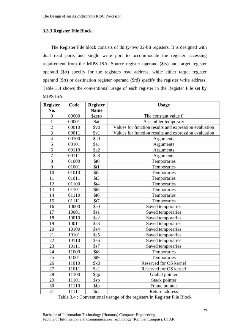
3.3.3 Register File Block
The Register File block consists of thirty-two 32-bit registers. It is designed with
dual read ports and single write port to accommodate the register accessing
requirement from the MIPS ISA. Source register operand ($rs) and target register
operand ($rt) specify for the registers read address, while either target register
operand ($rt) or destination register operand ($rd) specify the register write address.
Table 3.4 shows the conventional usage of each register in the Register File set by
MIPS ISA.
Register
No.
Code Register
Name
Usage
0 00000 $zero The constant value 0
1 00001 $at Assembler temporary
2 00010 $v0 Values for function results and expression evaluation
3 00011 $v1 Values for function results and expression evaluation
4 00100 $a0 Arguments
5 00101 $a1 Arguments
6 00110 $a2 Arguments
7 00111 $a3 Arguments
8 01000 $t0 Temporaries
9 01001 $t1 Temporaries
10 01010 $t2 Temporaries
11 01011 $t3 Temporaries
12 01100 $t4 Temporaries
13 01101 $t5 Temporaries
14 01110 $t6 Temporaries
15 01111 $t7 Temporaries
16 10000 $s0 Saved temporaries
17 10001 $s1 Saved temporaries
18 10010 $s2 Saved temporaries
19 10011 $s3 Saved temporaries
20 10100 $s4 Saved temporaries
21 10101 $s5 Saved temporaries
22 10110 $s6 Saved temporaries
23 10111 $s7 Saved temporaries
24 11000 $t8 Temporaries
25 11001 $t9 Temporaries
26 11010 $k0 Reserved for OS kernel
27 11011 $k1 Reserved for OS kernel
28 11100 $gp Global pointer
29 11101 $sp Stack pointer
30 11110 $fp Frame pointer
31 11111 $ra Return address
Table 3.4 : Conventional usange of the registers in Register File Block
The Design of An Asynchronous RISC Processor
30
Bachelor of Information Technology (Honours) Computer Engineering
Faculty of Information and Communication Technology (Kampar Campus), UTAR
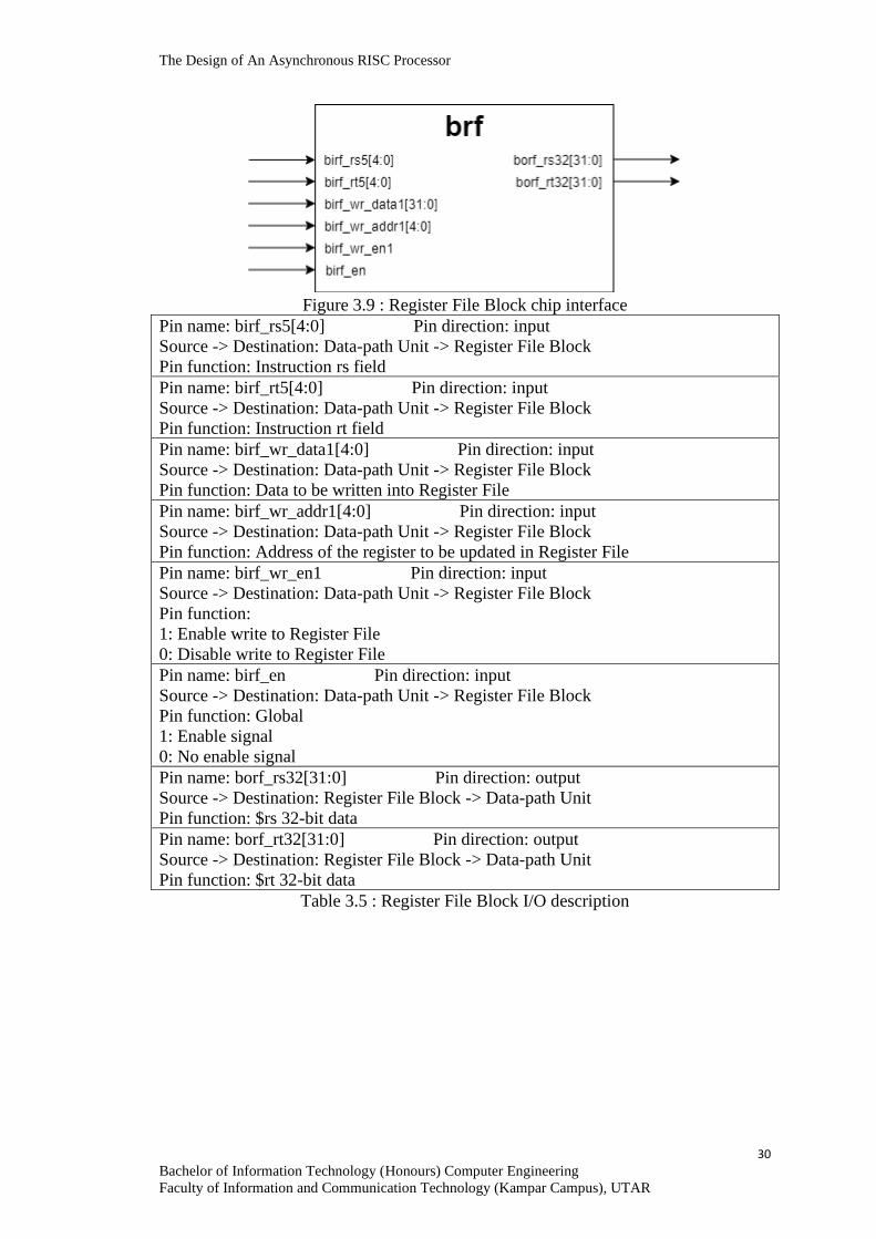
Figure 3.9 : Register File Block chip interface
Pin name: birf_rs5[4:0] Pin direction: input
Source -> Destination: Data-path Unit -> Register File Block
Pin function: Instruction rs field
Pin name: birf_rt5[4:0] Pin direction: input
Source -> Destination: Data-path Unit -> Register File Block
Pin function: Instruction rt field
Pin name: birf_wr_data1[4:0] Pin direction: input
Source -> Destination: Data-path Unit -> Register File Block
Pin function: Data to be written into Register File
Pin name: birf_wr_addr1[4:0] Pin direction: input
Source -> Destination: Data-path Unit -> Register File Block
Pin function: Address of the register to be updated in Register File
Pin name: birf_wr_en1 Pin direction: input
Source -> Destination: Data-path Unit -> Register File Block
Pin function:
1: Enable write to Register File
0: Disable write to Register File
Pin name: birf_en Pin direction: input
Source -> Destination: Data-path Unit -> Register File Block
Pin function: Global
1: Enable signal
0: No enable signal
Pin name: borf_rs32[31:0] Pin direction: output
Source -> Destination: Register File Block -> Data-path Unit
Pin function: $rs 32-bit data
Pin name: borf_rt32[31:0] Pin direction: output
Source -> Destination: Register File Block -> Data-path Unit
Pin function: $rt 32-bit data
Table 3.5 : Register File Block I/O description
The Design of An Asynchronous RISC Processor
31
Bachelor of Information Technology (Honours) Computer Engineering
Faculty of Information and Communication Technology (Kampar Campus), UTAR
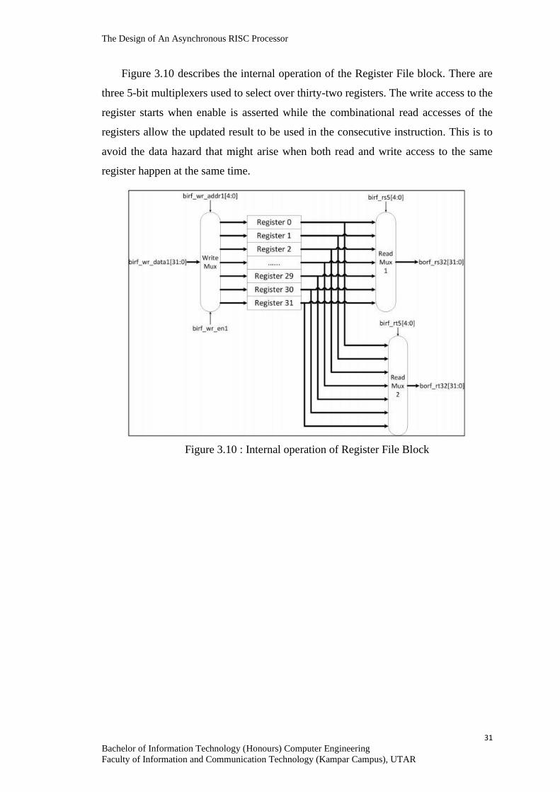
Figure 3.10 describes the internal operation of the Register File block. There are
three 5-bit multiplexers used to select over thirty-two registers. The write access to the
register starts when enable is asserted while the combinational read accesses of the
registers allow the updated result to be used in the consecutive instruction. This is to
avoid the data hazard that might arise when both read and write access to the same
register happen at the same time.
Figure 3.10 : Internal operation of Register File Block
The Design of An Asynchronous RISC Processor
32
Bachelor of Information Technology (Honours) Computer Engineering
Faculty of Information and Communication Technology (Kampar Campus), UTAR
3.3.4 Forwarding Block
Data hazards exist when the processor is designed in the pipeline structure. Data
hazard occurs due to Read-after-Write (RAW) data dependency. According to MIPS
ISA, Register File block will only be updated at WB stage. Both read (ID stage) and
write (WB stage) to Register File block is occurred in two different stages, thus, an
instruction may attempt to read Register File block before it is updated with the latest
data. Our approach resolves all the data hazards (except load-use hazard) that might
arise within the range of basic MIPS ISA core instructions, using the Forwarding
block. The data hazards that can be resolved using data forwarding are divided into 4
groups in relation to the system registers: General Condition of Register File, $ra
Register, Load-store and HILO Register.
For General Condition of Register File related data hazards, the data forwarding
is performed as earlier as possible, i.e. from EX or MEM stages to ID stage. This can
reduce the power consumption and pipeline size due to lesser control unit signals
passing through the pipeline structure. Another small advantage is to balance the stage
propagation delay of ID and EX stage: the propagation delay of ALU in EX stage is
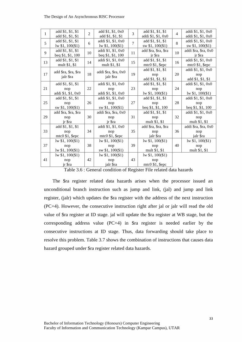
longer than RF in ID stage. Table 3.6 shows the combination of instructions that
causes data hazard grouped under general condition of Register File related data
hazards.
The Design of An Asynchronous RISC Processor
33
Bachelor of Information Technology (Honours) Computer Engineering
Faculty of Information and Communication Technology (Kampar Campus), UTAR
1 add $1, $1, $1
add $1, $1, $1 2
add $1, $1, 0x0
add $1, $1, $1 3
add $1, $1, $1
addi $1, $1, 0x0 4
addi $1, $1, 0x0
addi $1, $1, 0x0
5 add $1, $1, $1
lw $1, 100($1) 6
addi $1, $1, 0x0
lw $1, 100($1) 7
add $1, $1, $1
sw $1, 100($1) 8
addi $1, $1, 0x0
sw $1, 100($1)
9 add $1, $1, $1
beq $1, $1, 100 10
addi $1, $1, 0x0
beq $1, $1, 100 11
add $ra, $ra, $ra
jr $ra 10
addi $ra, $ra, 0x0
jr $ra
13 add $1, $1, $1
mult $1, $1 14
addi $1, $1, 0x0
mult $1, $1 15
add $1, $1, $1
mtc0 $1, $epc 16
addi $1, $1, 0x0
mtc0 $1, $epc
17 add $ra, $ra, $ra
jalr $ra 18
addi $ra, $ra, 0x0
jalr $ra 19
add $1, $1, $1
nop
add $1, $1, $1
20
addi $1, $1, 0x0
nop
add $1, $1, $1
21
add $1, $1, $1
nop
addi $1, $1, 0x0
22
addi $1, $1, 0x0
nop
addi $1, $1, 0x0
23
add $1, $1, $1
nop
lw $1, 100($1)
24
addi $1, $1, 0x0
nop
lw $1, 100($1)
25
add $1, $1, $1
nop
sw $1, 100($1)
26
addi $1, $1, 0x0
nop
sw $1, 100($1)
27
add $1, $1, $1
nop
beq $1, $1, 100
28
addi $1, $1, 0x0
nop
beq $1, $1, 100
29
add $ra, $ra, $ra
nop
jr $ra
30
addi $ra, $ra, 0x0
nop
jr $ra
31
add $1, $1, $1
nop
mult $1, $1
32
addi $1, $1, 0x0
nop
mult $1, $1
33
add $1, $1, $1
nop
mtc0 $1, $epc
34
addi $1, $1, 0x0
nop
mtc0 $1, $epc
35
add $ra, $ra, $ra
nop
jalr $ra
36
addi $ra, $ra, 0x0
nop
jalr $ra
37
lw $1, 100($1)
nop
lw $1, 100($1)
38
lw $1, 100($1)
nop
sw $1, 100($1)
39
lw $1, 100($1)
nop
mult $1, $1
40
lw $1, 100($1)
nop
mult $1, $1
41
lw $1, 100($1)
nop
jr $ra
42
lw $1, 100($1)
nop
jalr $ra
43
lw $1, 100($1)
nop
mtc0 $1, $epc
Table 3.6 : General condition of Register File related data hazards
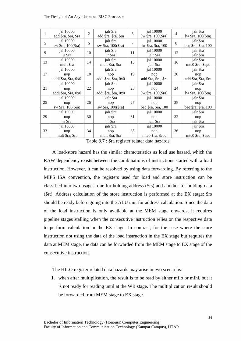
The $ra register related data hazards arises when the processor issued an
unconditional branch instruction such as jump and link, (jal) and jump and link
register, (jalr) which updates the $ra register with the address of the next instruction
(PC+4). However, the consecutive instruction right after jal or jalr will read the old
value of $ra register at ID stage. jal will update the $ra register at WB stage, but the
corresponding address value (PC+4) in $ra register is needed earlier by the
consecutive instructions at ID stage. Thus, data forwarding should take place to
resolve this problem. Table 3.7 shows the combination of instructions that causes data
hazard grouped under $ra register related data hazards.
The Design of An Asynchronous RISC Processor
34
Bachelor of Information Technology (Honours) Computer Engineering
Faculty of Information and Communication Technology (Kampar Campus), UTAR
1 jal 10000
add $ra, $ra, $ra 2
jalr $ra
add $ra, $ra, $ra 3
jal 10000
lw $ra, 100($ra) 4
jalr $ra
lw $ra, 100($ra)
5 jal 10000
sw $ra, 100($ra) 6
jalr $ra
sw $ra, 100($ra) 7
jal 10000
lw $ra, $ra, 100 8
jalr $ra
beq $ra, $ra, 100
9 jal 10000
jr $ra 10
jalr $ra
jr $ra 11
jal 10000
jalr $ra 12
jalr $ra
jalr $ra
13 jal 10000
mult $ra 14
jalr $ra
mult $ra, $ra 15
jal 10000
jalr $ra 16
jalr $ra
mtc0 $ra, $epc
17
jal 10000
nop
addi $ra, $ra, 0x0
18
jalr $ra
nop
addi $ra, $ra, 0x0
19
jal 10000
nop
add $ra, $ra, $ra
20
jalr $ra
nop
add $ra, $ra, $ra
21
jal 10000
nop
addi $ra, $ra, 0x0
22
jalr $ra
nop
addi $ra, $ra, 0x0
23
jal 10000
nop
lw $ra, 100($ra)
24
jalr $ra
nop
lw $ra, 100($ra)
25
jal 10000
nop
sw $ra, 100($ra)
26
kalr $ra
nop
sw $ra, 100($ra)
27
jal 10000
nop
beq $ra, $ra, 100
28
jalr $ra
nop
beq $ra, $ra, 100
29
jal 10000
nop
jr $ra
30
jalr $ra
nop
jr $ra
31
jal 10000
nop
jalr $ra
32
jalr $ra
nop
jalr $ra
33
jal 10000
nop
mult $ra, $ra
34
jalr $ra
nop
mult $ra, $ra
35
jal 10000
nop
mtc0 $ra, $epc
36
jalr $ra
nop
mtc0 $ra, $epc
Table 3.7 : $ra register relater data hazards
A load-store hazard has the similar characteristics as load use hazard, which the
RAW dependency exists between the combinations of instructions started with a load
instruction. However, it can be resolved by using data forwarding. By referring to the
MIPS ISA convention, the registers used for load and store instruction can be
classified into two usages, one for holding address ($rs) and another for holding data
($rt). Address calculation of the store instruction is performed at the EX stage: $rs
should be ready before going into the ALU unit for address calculation. Since the data
of the load instruction is only available at the MEM stage onwards, it requires
pipeline stages stalling when the consecutive instruction relies on the respective data
to perform calculation in the EX stage. In contrast, for the case where the store
instruction not using the data of the load instruction in the EX stage but requires the
data at MEM stage, the data can be forwarded from the MEM stage to EX stage of the
consecutive instruction.
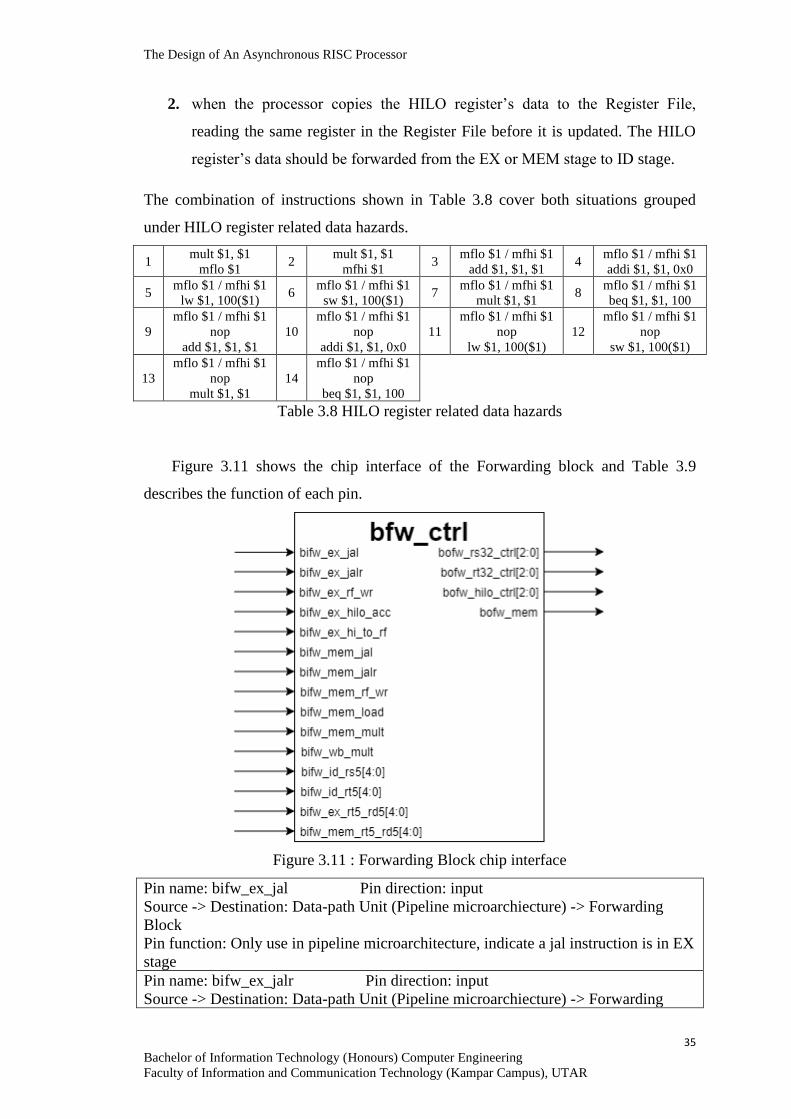
The HILO register related data hazards may arise in two scenarios:
1. when after multiplication, the result is to be read by either mflo or mfhi, but it
is not ready for reading until at the WB stage. The multiplication result should
be forwarded from MEM stage to EX stage.
The Design of An Asynchronous RISC Processor
35
Bachelor of Information Technology (Honours) Computer Engineering
Faculty of Information and Communication Technology (Kampar Campus), UTAR
2. when the processor copies the HILO register’s data to the Register File,
reading the same register in the Register File before it is updated. The HILO
register’s data should be forwarded from the EX or MEM stage to ID stage.
The combination of instructions shown in Table 3.8 cover both situations grouped
under HILO register related data hazards.
1 mult $1, $1
mflo $1 2
mult $1, $1
mfhi $1 3
mflo $1 / mfhi $1
add $1, $1, $1 4
mflo $1 / mfhi $1
addi $1, $1, 0x0
5 mflo $1 / mfhi $1
lw $1, 100($1) 6
mflo $1 / mfhi $1
sw $1, 100($1) 7
mflo $1 / mfhi $1
mult $1, $1 8
mflo $1 / mfhi $1
beq $1, $1, 100
9
mflo $1 / mfhi $1
nop
add $1, $1, $1
10
mflo $1 / mfhi $1
nop
addi $1, $1, 0x0
11
mflo $1 / mfhi $1
nop
lw $1, 100($1)
12
mflo $1 / mfhi $1
nop
sw $1, 100($1)
13
mflo $1 / mfhi $1
nop
mult $1, $1
14
mflo $1 / mfhi $1
nop
beq $1, $1, 100
Table 3.8 HILO register related data hazards
Figure 3.11 shows the chip interface of the Forwarding block and Table 3.9
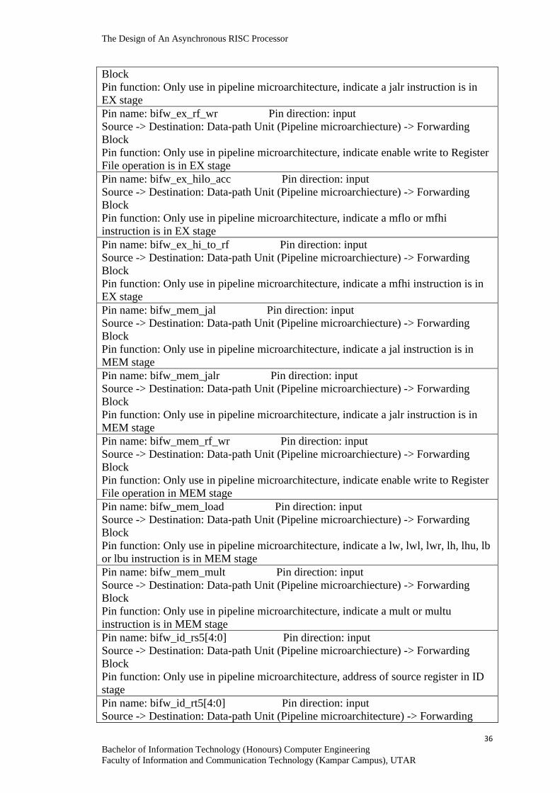
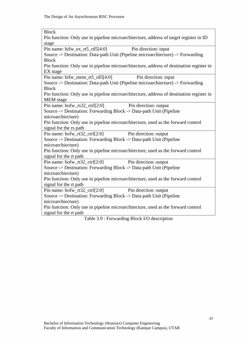
describes the function of each pin.
Figure 3.11 : Forwarding Block chip interface
Pin name: bifw_ex_jal Pin direction: input
Source -> Destination: Data-path Unit (Pipeline microarchiecture) -> Forwarding
Block
Pin function: Only use in pipeline microarchitecture, indicate a jal instruction is in EX
stage
Pin name: bifw_ex_jalr Pin direction: input
Source -> Destination: Data-path Unit (Pipeline microarchiecture) -> Forwarding
The Design of An Asynchronous RISC Processor
36
Bachelor of Information Technology (Honours) Computer Engineering
Faculty of Information and Communication Technology (Kampar Campus), UTAR
Block
Pin function: Only use in pipeline microarchitecture, indicate a jalr instruction is in
EX stage
Pin name: bifw_ex_rf_wr Pin direction: input
Source -> Destination: Data-path Unit (Pipeline microarchiecture) -> Forwarding
Block
Pin function: Only use in pipeline microarchitecture, indicate enable write to Register
File operation is in EX stage
Pin name: bifw_ex_hilo_acc Pin direction: input
Source -> Destination: Data-path Unit (Pipeline microarchiecture) -> Forwarding
Block
Pin function: Only use in pipeline microarchitecture, indicate a mflo or mfhi
instruction is in EX stage
Pin name: bifw_ex_hi_to_rf Pin direction: input
Source -> Destination: Data-path Unit (Pipeline microarchiecture) -> Forwarding
Block
Pin function: Only use in pipeline microarchitecture, indicate a mfhi instruction is in
EX stage
Pin name: bifw_mem_jal Pin direction: input
Source -> Destination: Data-path Unit (Pipeline microarchiecture) -> Forwarding
Block
Pin function: Only use in pipeline microarchitecture, indicate a jal instruction is in
MEM stage
Pin name: bifw_mem_jalr Pin direction: input
Source -> Destination: Data-path Unit (Pipeline microarchiecture) -> Forwarding
Block
Pin function: Only use in pipeline microarchitecture, indicate a jalr instruction is in
MEM stage
Pin name: bifw_mem_rf_wr Pin direction: input
Source -> Destination: Data-path Unit (Pipeline microarchiecture) -> Forwarding
Block
Pin function: Only use in pipeline microarchitecture, indicate enable write to Register
File operation in MEM stage
Pin name: bifw_mem_load Pin direction: input
Source -> Destination: Data-path Unit (Pipeline microarchiecture) -> Forwarding
Block
Pin function: Only use in pipeline microarchitecture, indicate a lw, lwl, lwr, lh, lhu, lb
or lbu instruction is in MEM stage
Pin name: bifw_mem_mult Pin direction: input
Source -> Destination: Data-path Unit (Pipeline microarchiecture) -> Forwarding
Block
Pin function: Only use in pipeline microarchitecture, indicate a mult or multu
instruction is in MEM stage
Pin name: bifw_id_rs5[4:0] Pin direction: input
Source -> Destination: Data-path Unit (Pipeline microarchiecture) -> Forwarding
Block
Pin function: Only use in pipeline microarchitecture, address of source register in ID
stage
Pin name: bifw_id_rt5[4:0] Pin direction: input
Source -> Destination: Data-path Unit (Pipeline microarchitecture) -> Forwarding
The Design of An Asynchronous RISC Processor
37
Bachelor of Information Technology (Honours) Computer Engineering
Faculty of Information and Communication Technology (Kampar Campus), UTAR
Block
Pin function: Only use in pipeline microarchitecture, address of target register in ID
stage
Pin name: bifw_ex_rt5_rd5[4:0] Pin direction: input
Source -> Destination: Data-path Unit (Pipeline microarchiecture) -> Forwarding
Block
Pin function: Only use in pipeline microarchitecture, address of destination register in
EX stage
Pin name: bifw_mem_rt5_rd5[4:0] Pin direction: input
Source -> Destination: Data-path Unit (Pipeline microarchiecture) -> Forwarding
Block
Pin function: Only use in pipeline microarchitecture, address of destination register in
MEM stage
Pin name: bofw_rs32_ctrl[2:0] Pin direction: output
Source -> Destination: Forwarding Block -> Data-path Unit (Pipeline
microarchiecture)
Pin function: Only use in pipeline microarchitecture, used as the forward control
signal for the rs path
Pin name: bofw_rt32_ctrl[2:0] Pin direction: output
Source -> Destination: Forwarding Block -> Data-path Unit (Pipeline
microarchiecture)
Pin function: Only use in pipeline microarchitecture, used as the forward control
signal for the rt path
Pin name: bofw_rt32_ctrl[2:0] Pin direction: output
Source -> Destination: Forwarding Block -> Data-path Unit (Pipeline
microarchiecture)
Pin function: Only use in pipeline microarchitecture, used as the forward control
signal for the rt path
Pin name: bofw_rt32_ctrl[2:0] Pin direction: output
Source -> Destination: Forwarding Block -> Data-path Unit (Pipeline
microarchiecture)
Pin function: Only use in pipeline microarchitecture, used as the forward control
signal for the rt path
Table 3.9 : Forwarding Block I/O description
The Design of An Asynchronous RISC Processor
38
Bachelor of Information Technology (Honours) Computer Engineering
Faculty of Information and Communication Technology (Kampar Campus), UTAR
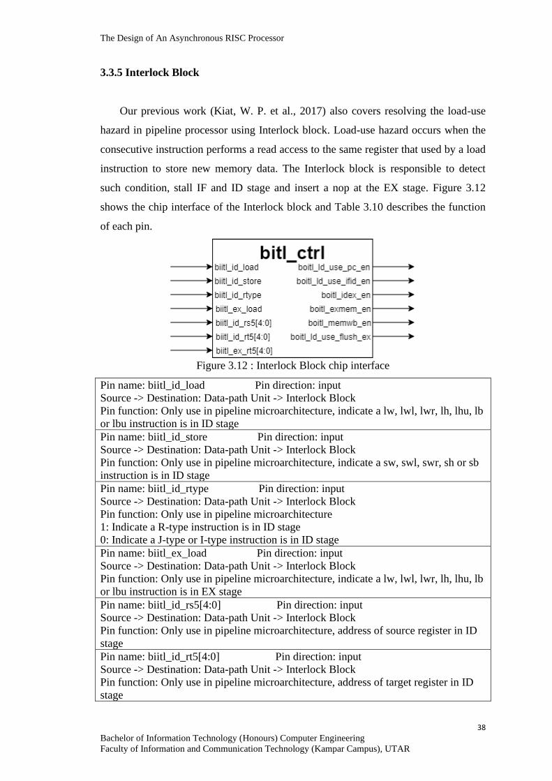
3.3.5 Interlock Block
Our previous work (Kiat, W. P. et al., 2017) also covers resolving the load-use
hazard in pipeline processor using Interlock block. Load-use hazard occurs when the
consecutive instruction performs a read access to the same register that used by a load
instruction to store new memory data. The Interlock block is responsible to detect
such condition, stall IF and ID stage and insert a nop at the EX stage. Figure 3.12
shows the chip interface of the Interlock block and Table 3.10 describes the function
of each pin.
Figure 3.12 : Interlock Block chip interface
Pin name: biitl_id_load Pin direction: input
Source -> Destination: Data-path Unit -> Interlock Block
Pin function: Only use in pipeline microarchitecture, indicate a lw, lwl, lwr, lh, lhu, lb
or lbu instruction is in ID stage
Pin name: biitl_id_store Pin direction: input
Source -> Destination: Data-path Unit -> Interlock Block
Pin function: Only use in pipeline microarchitecture, indicate a sw, swl, swr, sh or sb
instruction is in ID stage
Pin name: biitl_id_rtype Pin direction: input
Source -> Destination: Data-path Unit -> Interlock Block
Pin function: Only use in pipeline microarchitecture
1: Indicate a R-type instruction is in ID stage
0: Indicate a J-type or I-type instruction is in ID stage
Pin name: biitl_ex_load Pin direction: input
Source -> Destination: Data-path Unit -> Interlock Block
Pin function: Only use in pipeline microarchitecture, indicate a lw, lwl, lwr, lh, lhu, lb
or lbu instruction is in EX stage
Pin name: biitl_id_rs5[4:0] Pin direction: input
Source -> Destination: Data-path Unit -> Interlock Block
Pin function: Only use in pipeline microarchitecture, address of source register in ID
stage
Pin name: biitl_id_rt5[4:0] Pin direction: input
Source -> Destination: Data-path Unit -> Interlock Block
Pin function: Only use in pipeline microarchitecture, address of target register in ID
stage
The Design of An Asynchronous RISC Processor
39
Bachelor of Information Technology (Honours) Computer Engineering
Faculty of Information and Communication Technology (Kampar Campus), UTAR
Pin name: biitl_ex_rt5[4:0] Pin direction: input
Source -> Destination: Data-path Unit -> Interlock Block
Pin function: Only use in pipeline microarchitecture, address of target register in EX
stage
Pin name: boitl_ld_use_pc_en Pin direction: output
Source -> Destination: Interlock Block -> Data-path Unit
Pin function: Only use in pipeline microarchitecture
1: No stall on PC register
0: Stall PC register
Pin name: boitl_ld_use_ifid_en Pin direction: output
Source -> Destination: Interlock Block -> Data-path Unit
Pin function: Only use in pipeline microarchitecture
1: No stall on IF/ID pipeline register
0: Stall IF/ID pipeline register
Pin name: boitl_idex_en Pin direction: output
Source -> Destination: Interlock Block -> Data-path Unit
Pin function: Reserved for future development, temporary always enable
Pin name: boitl_exmem_en Pin direction: output
Source -> Destination: Interlock Block -> Data-path Unit
Pin function: Reserved for future development, temporary always enable
Pin name: boitl_memwb_en Pin direction: output
Source -> Destination: Interlock Block -> Data-path Unit
Pin function: Reserved for future development, temporary always enable
Pin name: boitl_ld_use_flush_ex Pin direction: output
Source -> Destination: Interlock Block -> Data-path Unit
Pin function: Only use in pipeline microarchitecture
1: Flush ID/EX stage pipeline register
0: No pipeline register flush is requires
Table 3.10 : Interlock Block I/O description
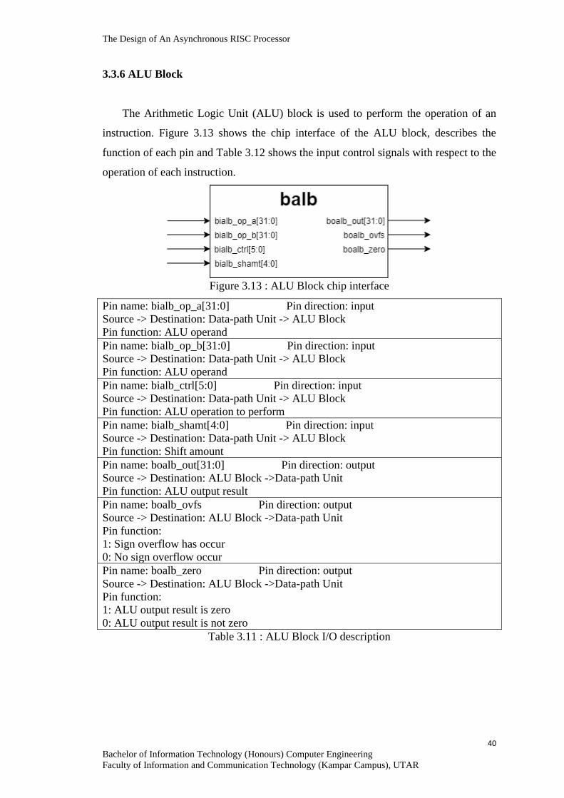
The Design of An Asynchronous RISC Processor
40
Bachelor of Information Technology (Honours) Computer Engineering
Faculty of Information and Communication Technology (Kampar Campus), UTAR
3.3.6 ALU Block
The Arithmetic Logic Unit (ALU) block is used to perform the operation of an
instruction. Figure 3.13 shows the chip interface of the ALU block, describes the
function of each pin and Table 3.12 shows the input control signals with respect to the
operation of each instruction.
Figure 3.13 : ALU Block chip interface
Pin name: bialb_op_a[31:0] Pin direction: input
Source -> Destination: Data-path Unit -> ALU Block
Pin function: ALU operand
Pin name: bialb_op_b[31:0] Pin direction: input
Source -> Destination: Data-path Unit -> ALU Block
Pin function: ALU operand
Pin name: bialb_ctrl[5:0] Pin direction: input
Source -> Destination: Data-path Unit -> ALU Block
Pin function: ALU operation to perform
Pin name: bialb_shamt[4:0] Pin direction: input
Source -> Destination: Data-path Unit -> ALU Block
Pin function: Shift amount
Pin name: boalb_out[31:0] Pin direction: output
Source -> Destination: ALU Block ->Data-path Unit
Pin function: ALU output result
Pin name: boalb_ovfs Pin direction: output
Source -> Destination: ALU Block ->Data-path Unit
Pin function:
1: Sign overflow has occur
0: No sign overflow occur
Pin name: boalb_zero Pin direction: output
Source -> Destination: ALU Block ->Data-path Unit
Pin function:
1: ALU output result is zero
0: ALU output result is not zero
Table 3.11 : ALU Block I/O description
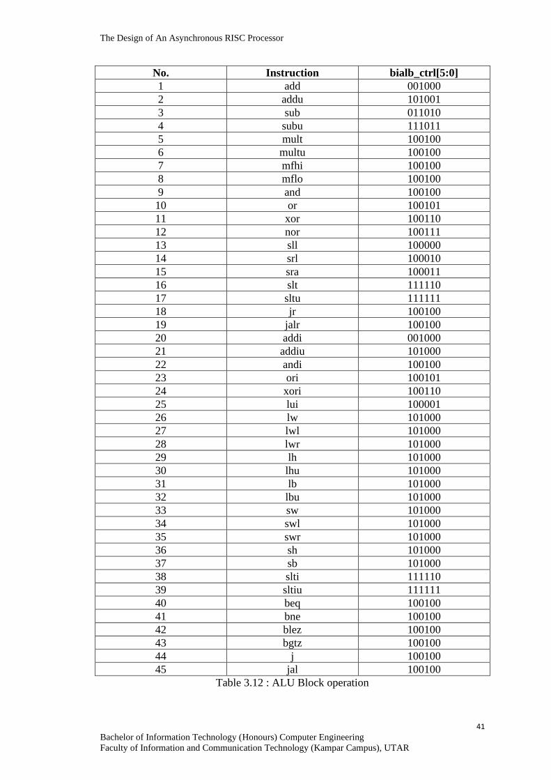
The Design of An Asynchronous RISC Processor
41
Bachelor of Information Technology (Honours) Computer Engineering
Faculty of Information and Communication Technology (Kampar Campus), UTAR
No. Instruction bialb_ctrl[5:0]
1 add 001000
2 addu 101001
3 sub 011010
4 subu 111011
5 mult 100100
6 multu 100100
7 mfhi 100100
8 mflo 100100
9 and 100100
10 or 100101
11 xor 100110
12 nor 100111
13 sll 100000
14 srl 100010
15 sra 100011
16 slt 111110
17 sltu 111111
18 jr 100100
19 jalr 100100
20 addi 001000
21 addiu 101000
22 andi 100100
23 ori 100101
24 xori 100110
25 lui 100001
26 lw 101000
27 lwl 101000
28 lwr 101000
29 lh 101000
30 lhu 101000
31 lb 101000
32 lbu 101000
33 sw 101000
34 swl 101000
35 swr 101000
36 sh 101000
37 sb 101000
38 slti 111110
39 sltiu 111111
40 beq 100100
41 bne 100100
42 blez 100100
43 bgtz 100100
44 j 100100
45 jal 100100
Table 3.12 : ALU Block operation
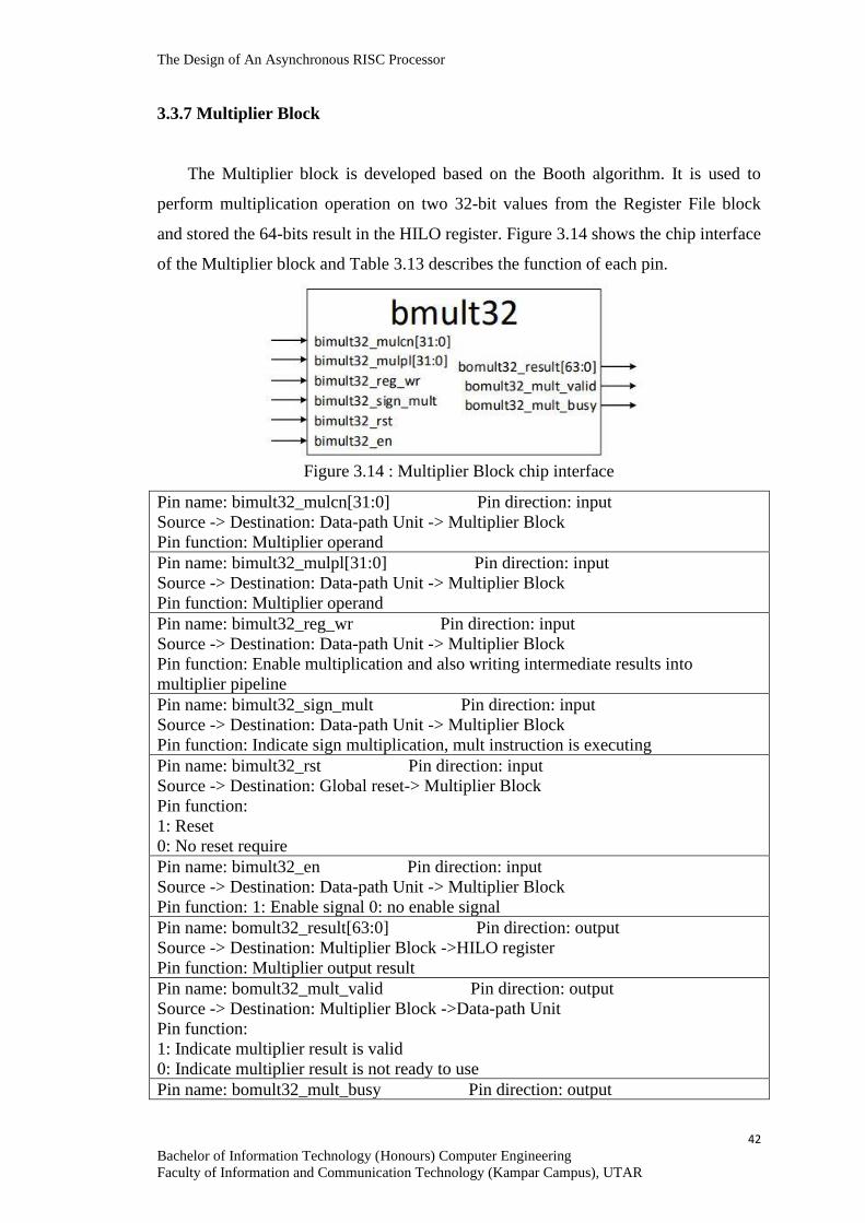
The Design of An Asynchronous RISC Processor
42
Bachelor of Information Technology (Honours) Computer Engineering
Faculty of Information and Communication Technology (Kampar Campus), UTAR
3.3.7 Multiplier Block
The Multiplier block is developed based on the Booth algorithm. It is used to
perform multiplication operation on two 32-bit values from the Register File block
and stored the 64-bits result in the HILO register. Figure 3.14 shows the chip interface
of the Multiplier block and Table 3.13 describes the function of each pin.
Figure 3.14 : Multiplier Block chip interface
Pin name: bimult32_mulcn[31:0] Pin direction: input
Source -> Destination: Data-path Unit -> Multiplier Block
Pin function: Multiplier operand
Pin name: bimult32_mulpl[31:0] Pin direction: input
Source -> Destination: Data-path Unit -> Multiplier Block
Pin function: Multiplier operand
Pin name: bimult32_reg_wr Pin direction: input
Source -> Destination: Data-path Unit -> Multiplier Block
Pin function: Enable multiplication and also writing intermediate results into
multiplier pipeline
Pin name: bimult32_sign_mult Pin direction: input
Source -> Destination: Data-path Unit -> Multiplier Block
Pin function: Indicate sign multiplication, mult instruction is executing
Pin name: bimult32_rst Pin direction: input
Source -> Destination: Global reset-> Multiplier Block
Pin function:
1: Reset
0: No reset require
Pin name: bimult32_en Pin direction: input
Source -> Destination: Data-path Unit -> Multiplier Block
Pin function: 1: Enable signal 0: no enable signal
Pin name: bomult32_result[63:0] Pin direction: output
Source -> Destination: Multiplier Block ->HILO register
Pin function: Multiplier output result
Pin name: bomult32_mult_valid Pin direction: output
Source -> Destination: Multiplier Block ->Data-path Unit
Pin function:
1: Indicate multiplier result is valid
0: Indicate multiplier result is not ready to use
Pin name: bomult32_mult_busy Pin direction: output
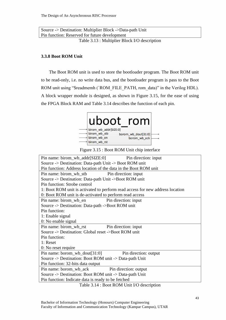
The Design of An Asynchronous RISC Processor
43
Bachelor of Information Technology (Honours) Computer Engineering
Faculty of Information and Communication Technology (Kampar Campus), UTAR
Source -> Destination: Multiplier Block ->Data-path Unit
Pin function: Reserved for future development
Table 3.13 : Multiplier Block I/O description
3.3.8 Boot ROM Unit
The Boot ROM unit is used to store the bootloader program. The Boot ROM unit
to be read-only, i.e. no write data bus, and the bootloader program is pass to the Boot
ROM unit using “$readmemh (`ROM_FILE_PATH, rom_data)” in the Verilog HDL).
A block wrapper module is designed, as shown in Figure 3.15, for the ease of using
the FPGA Block RAM and Table 3.14 describes the function of each pin.
Figure 3.15 : Boot ROM Unit chip interface
Pin name: birom_wb_addr[SIZE:0] Pin direction: input
Source -> Destination: Data-path Unit -> Boot ROM unit
Pin function: Address location of the data in the Boot ROM unit
Pin name: birom_wb_stb Pin direction: input
Source -> Destination: Data-path Unit ->Boot ROM unit
Pin function: Strobe control
1: Boot ROM unit is activated to perform read access for new address location
0: Boot ROM unit is de-activated to perform read access
Pin name: birom_wb_en Pin direction: input
Source -> Destination: Data-path ->Boot ROM unit
Pin function:
1: Enable signal
0: No enable signal
Pin name: birom_wb_rst Pin direction: input
Source -> Destination: Global reset ->Boot ROM unit
Pin function:
1: Reset
0: No reset require
Pin name: borom_wb_dout[31:0] Pin direction: output
Source -> Destination: Boot ROM unit -> Data-path Unit
Pin function: 32-bits data output
Pin name: borom_wb_ack Pin direction: output
Source -> Destination: Boot ROM unit -> Data-path Unit
Pin function: Indicate data is ready to be fetched
Table 3.14 : Boot ROM Unit I/O description
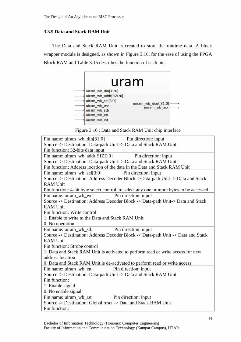
The Design of An Asynchronous RISC Processor
44
Bachelor of Information Technology (Honours) Computer Engineering
Faculty of Information and Communication Technology (Kampar Campus), UTAR
3.3.9 Data and Stack RAM Unit
The Data and Stack RAM Unit is created to store the runtime data. A block
wrapper module is designed, as shown in Figure 3.16, for the ease of using the FPGA
Block RAM and Table 3.15 describes the function of each pin.
Figure 3.16 : Data and Stack RAM Unit chip interface
Pin name: uiram_wb_din[31:0] Pin direction: input
Source -> Destination: Data-path Unit -> Data and Stack RAM Unit
Pin function: 32-bits data input
Pin name: uiram_wb_addr[SIZE:0] Pin direction: input
Source -> Destination: Data-path Unit -> Data and Stack RAM Unit
Pin function: Address location of the data in the Data and Stack RAM Unit
Pin name: uiram_wb_sel[3:0] Pin direction: input
Source -> Destination: Address Decoder Block ->Data-path Unit -> Data and Stack
RAM Unit
Pin function: 4-bit byte select control, to select any one or more bytes to be accessed
Pin name: uiram_wb_we Pin direction: input
Source -> Destination: Address Decoder Block -> Data-path Unit-> Data and Stack
RAM Unit
Pin function: Write control
1: Enable to write to the Data and Stack RAM Unit
0: No operation
Pin name: uiram_wb_stb Pin direction: input
Source -> Destination: Address Decoder Block -> Data-path Unit -> Data and Stack
RAM Unit
Pin function: Strobe control
1: Data and Stack RAM Unit is activated to perform read or write access for new
address location
0: Data and Stack RAM Unit is de-activated to perform read or write access
Pin name: uiram_wb_en Pin direction: input
Source -> Destination: Data-path Unit -> Data and Stack RAM Unit
Pin function:
1: Enable signal
0: No enable signal
Pin name: uiram_wb_rst Pin direction: input
Source -> Destination: Global reset -> Data and Stack RAM Unit
Pin function:
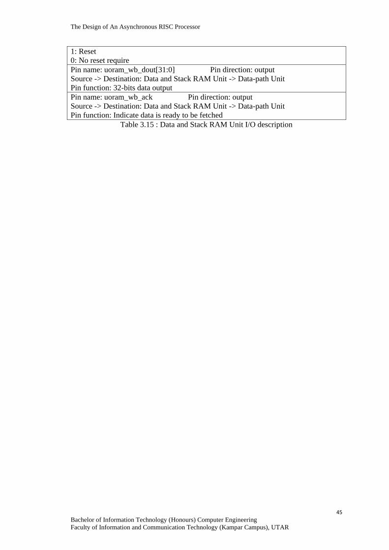
The Design of An Asynchronous RISC Processor
45
Bachelor of Information Technology (Honours) Computer Engineering
Faculty of Information and Communication Technology (Kampar Campus), UTAR
1: Reset
0: No reset require
Pin name: uoram_wb_dout[31:0] Pin direction: output
Source -> Destination: Data and Stack RAM Unit -> Data-path Unit
Pin function: 32-bits data output
Pin name: uoram_wb_ack Pin direction: output
Source -> Destination: Data and Stack RAM Unit -> Data-path Unit
Pin function: Indicate data is ready to be fetched
Table 3.15 : Data and Stack RAM Unit I/O description
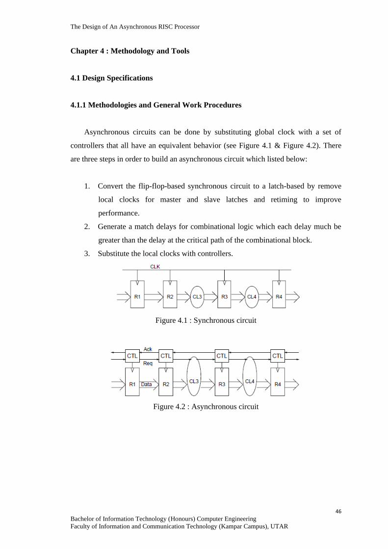
The Design of An Asynchronous RISC Processor
46
Bachelor of Information Technology (Honours) Computer Engineering
Faculty of Information and Communication Technology (Kampar Campus), UTAR
Chapter 4 : Methodology and Tools
4.1 Design Specifications
4.1.1 Methodologies and General Work Procedures
Asynchronous circuits can be done by substituting global clock with a set of
controllers that all have an equivalent behavior (see Figure 4.1 & Figure 4.2). There
are three steps in order to build an asynchronous circuit which listed below:
1. Convert the flip-flop-based synchronous circuit to a latch-based by remove
local clocks for master and slave latches and retiming to improve
performance.
2. Generate a match delays for combinational logic which each delay much be
greater than the delay at the critical path of the combinational block.
3. Substitute the local clocks with controllers.
Figure 4.1 : Synchronous circuit
Figure 4.2 : Asynchronous circuit
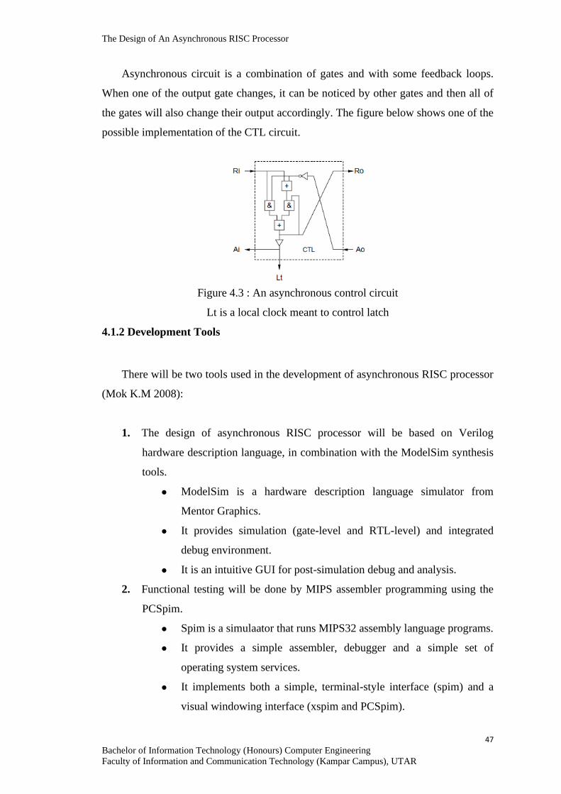
The Design of An Asynchronous RISC Processor
47
Bachelor of Information Technology (Honours) Computer Engineering
Faculty of Information and Communication Technology (Kampar Campus), UTAR
Asynchronous circuit is a combination of gates and with some feedback loops.
When one of the output gate changes, it can be noticed by other gates and then all of
the gates will also change their output accordingly. The figure below shows one of the
possible implementation of the CTL circuit.
Figure 4.3 : An asynchronous control circuit
Lt is a local clock meant to control latch
4.1.2 Development Tools
There will be two tools used in the development of asynchronous RISC processor
(Mok K.M 2008):
1. The design of asynchronous RISC processor will be based on Verilog
hardware description language, in combination with the ModelSim synthesis
tools.
⚫ ModelSim is a hardware description language simulator from
Mentor Graphics.
⚫ It provides simulation (gate-level and RTL-level) and integrated
debug environment.
⚫ It is an intuitive GUI for post-simulation debug and analysis.
2. Functional testing will be done by MIPS assembler programming using the
PCSpim.
⚫ Spim is a simulaator that runs MIPS32 assembly language programs.
⚫ It provides a simple assembler, debugger and a simple set of
operating system services.
⚫ It implements both a simple, terminal-style interface (spim) and a
visual windowing interface (xspim and PCSpim).
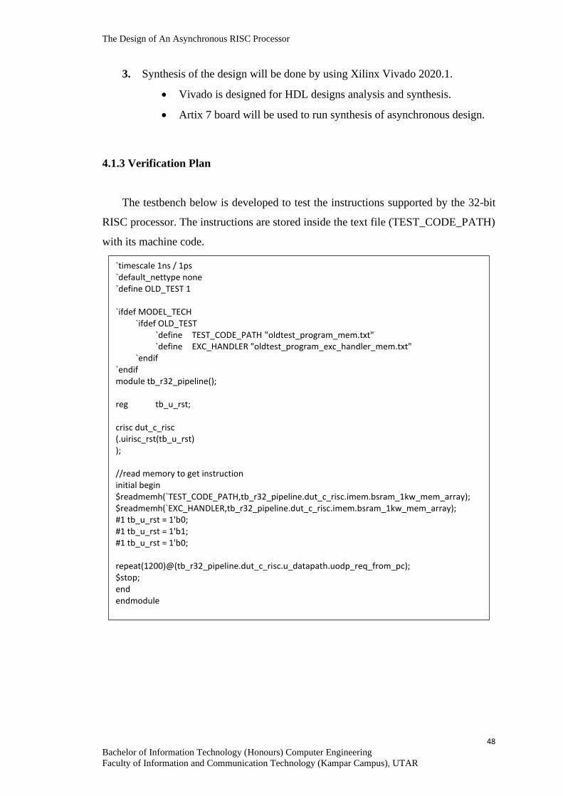
The Design of An Asynchronous RISC Processor
48
Bachelor of Information Technology (Honours) Computer Engineering
Faculty of Information and Communication Technology (Kampar Campus), UTAR
3. Synthesis of the design will be done by using Xilinx Vivado 2020.1.
• Vivado is designed for HDL designs analysis and synthesis.
• Artix 7 board will be used to run synthesis of asynchronous design.
4.1.3 Verification Plan
The testbench below is developed to test the instructions supported by the 32-bit
RISC processor. The instructions are stored inside the text file (TEST_CODE_PATH)
with its machine code.
`timescale 1ns / 1ps `default_nettype none `define OLD_TEST 1 `ifdef MODEL_TECH `ifdef OLD_TEST `define TEST_CODE_PATH "oldtest_program_mem.txt" `define EXC_HANDLER "oldtest_program_exc_handler_mem.txt" `endif `endif module tb_r32_pipeline(); reg tb_u_rst; crisc dut_c_risc (.uirisc_rst(tb_u_rst) ); //read memory to get instruction initial begin $readmemh(`TEST_CODE_PATH,tb_r32_pipeline.dut_c_risc.imem.bsram_1kw_mem_array); $readmemh(`EXC_HANDLER,tb_r32_pipeline.dut_c_risc.imem.bsram_1kw_mem_array); #1 tb_u_rst = 1'b0; #1 tb_u_rst = 1'b1; #1 tb_u_rst = 1'b0; repeat(1200)@(tb_r32_pipeline.dut_c_risc.u_datapath.uodp_req_from_pc); $stop; end endmodule
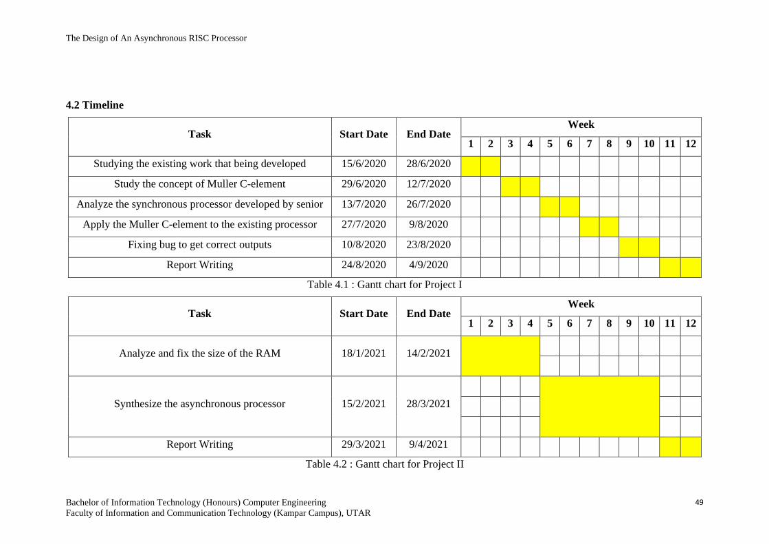
The Design of An Asynchronous RISC Processor
Bachelor of Information Technology (Honours) Computer Engineering
Faculty of Information and Communication Technology (Kampar Campus), UTAR
49
4.2 Timeline
Task Start Date End Date Week
1 2 3 4 5 6 7 8 9 10 11 12
Studying the existing work that being developed 15/6/2020 28/6/2020
Study the concept of Muller C-element 29/6/2020 12/7/2020
Analyze the synchronous processor developed by senior 13/7/2020 26/7/2020
Apply the Muller C-element to the existing processor 27/7/2020 9/8/2020
Fixing bug to get correct outputs 10/8/2020 23/8/2020
Report Writing 24/8/2020 4/9/2020
Table 4.1 : Gantt chart for Project I
Task Start Date End Date Week
1 2 3 4 5 6 7 8 9 10 11 12
Analyze and fix the size of the RAM 18/1/2021 14/2/2021
Synthesize the asynchronous processor 15/2/2021 28/3/2021
Report Writing 29/3/2021 9/4/2021
Table 4.2 : Gantt chart for Project II
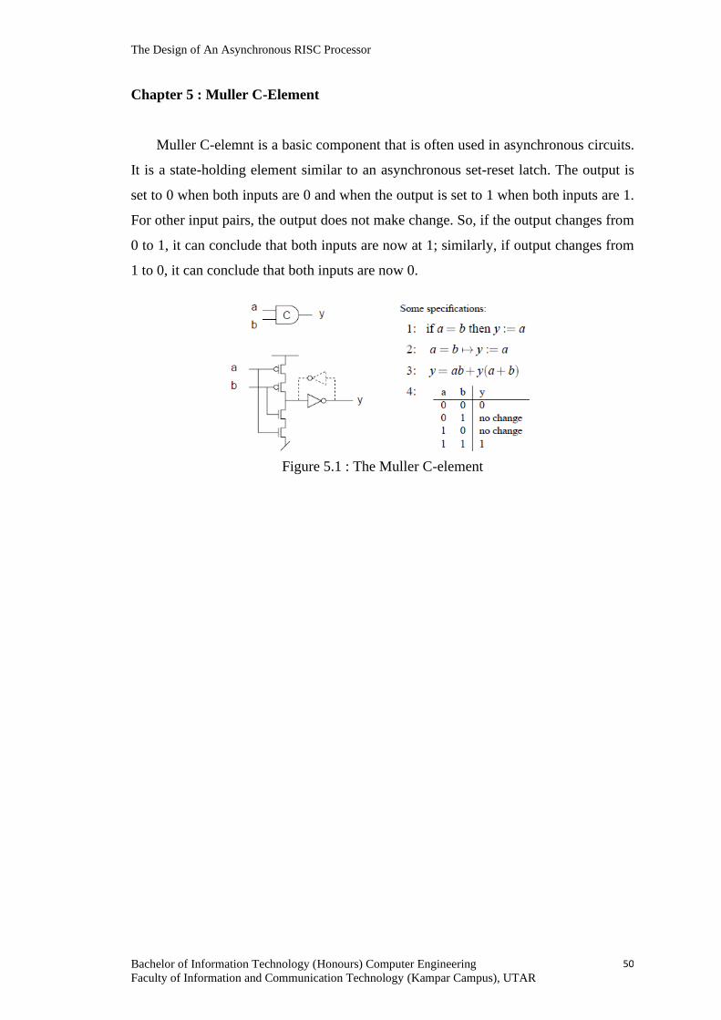
The Design of An Asynchronous RISC Processor
Bachelor of Information Technology (Honours) Computer Engineering
Faculty of Information and Communication Technology (Kampar Campus), UTAR
50
Chapter 5 : Muller C-Element
Muller C-elemnt is a basic component that is often used in asynchronous circuits.
It is a state-holding element similar to an asynchronous set-reset latch. The output is
set to 0 when both inputs are 0 and when the output is set to 1 when both inputs are 1.
For other input pairs, the output does not make change. So, if the output changes from
0 to 1, it can conclude that both inputs are now at 1; similarly, if output changes from
1 to 0, it can conclude that both inputs are now 0.
Figure 5.1 : The Muller C-element
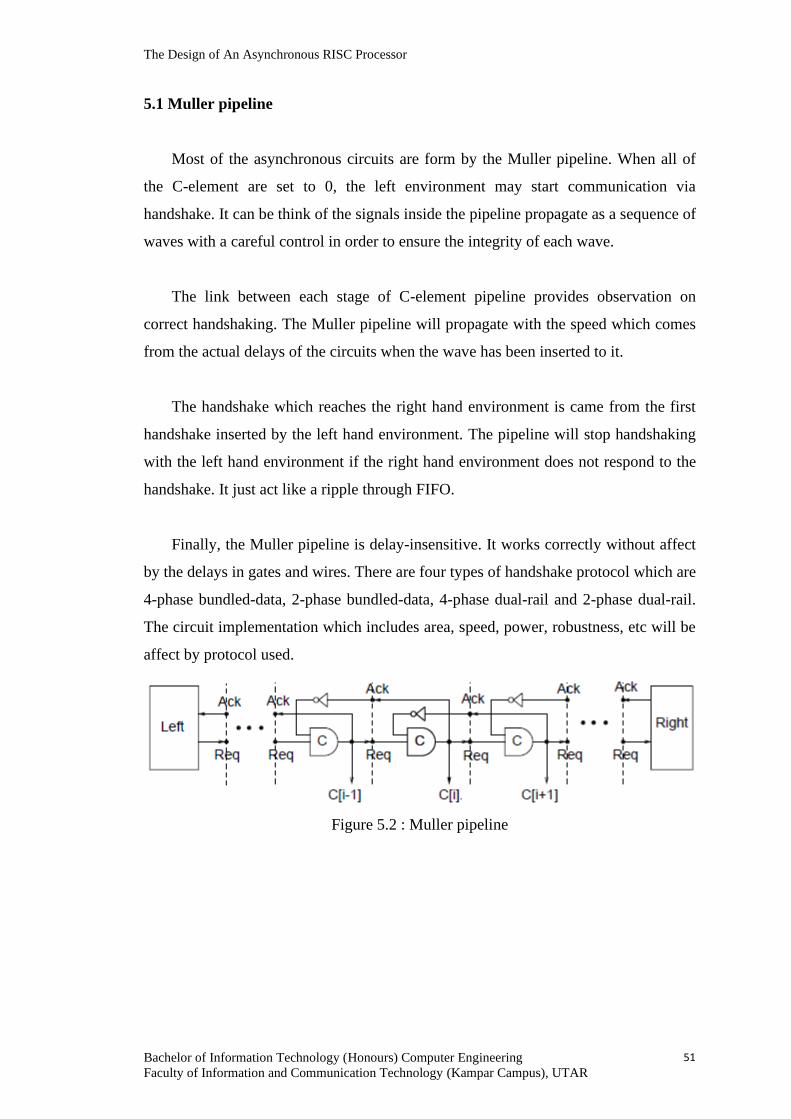
The Design of An Asynchronous RISC Processor
Bachelor of Information Technology (Honours) Computer Engineering
Faculty of Information and Communication Technology (Kampar Campus), UTAR
51
5.1 Muller pipeline
Most of the asynchronous circuits are form by the Muller pipeline. When all of
the C-element are set to 0, the left environment may start communication via
handshake. It can be think of the signals inside the pipeline propagate as a sequence of
waves with a careful control in order to ensure the integrity of each wave.
The link between each stage of C-element pipeline provides observation on
correct handshaking. The Muller pipeline will propagate with the speed which comes
from the actual delays of the circuits when the wave has been inserted to it.
The handshake which reaches the right hand environment is came from the first
handshake inserted by the left hand environment. The pipeline will stop handshaking
with the left hand environment if the right hand environment does not respond to the
handshake. It just act like a ripple through FIFO.
Finally, the Muller pipeline is delay-insensitive. It works correctly without affect
by the delays in gates and wires. There are four types of handshake protocol which are
4-phase bundled-data, 2-phase bundled-data, 4-phase dual-rail and 2-phase dual-rail.
The circuit implementation which includes area, speed, power, robustness, etc will be
affect by protocol used.
Figure 5.2 : Muller pipeline
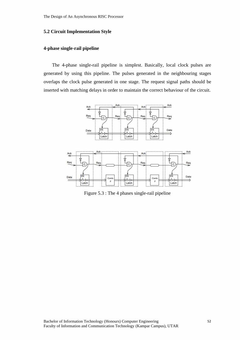
The Design of An Asynchronous RISC Processor
Bachelor of Information Technology (Honours) Computer Engineering
Faculty of Information and Communication Technology (Kampar Campus), UTAR
52
5.2 Circuit Implementation Style
4-phase single-rail pipeline
The 4-phase single-rail pipeline is simplest. Basically, local clock pulses are
generated by using this pipeline. The pulses generated in the neighbouring stages
overlaps the clock pulse generated in one stage. The request signal paths should be
inserted with matching delays in order to maintain the correct behaviour of the circuit.
Figure 5.3 : The 4 phases single-rail pipeline
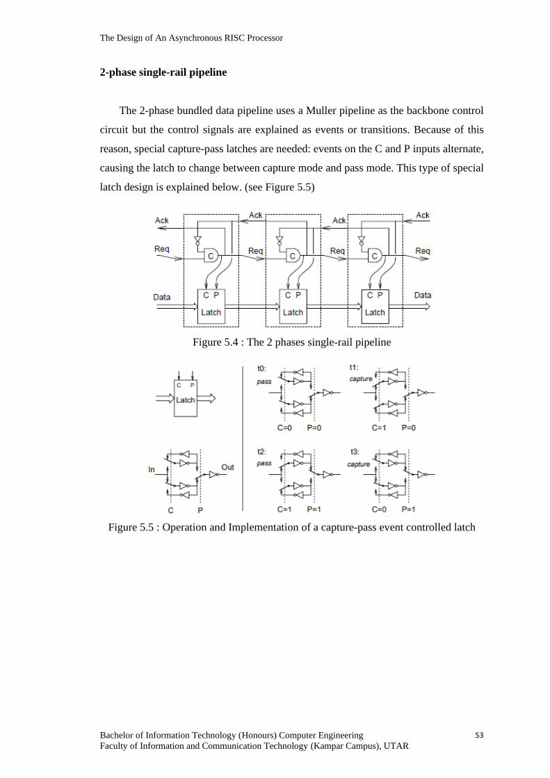
The Design of An Asynchronous RISC Processor
Bachelor of Information Technology (Honours) Computer Engineering
Faculty of Information and Communication Technology (Kampar Campus), UTAR
53
2-phase single-rail pipeline
The 2-phase bundled data pipeline uses a Muller pipeline as the backbone control
circuit but the control signals are explained as events or transitions. Because of this
reason, special capture-pass latches are needed: events on the C and P inputs alternate,
causing the latch to change between capture mode and pass mode. This type of special
latch design is explained below. (see Figure 5.5)
Figure 5.4 : The 2 phases single-rail pipeline
Figure 5.5 : Operation and Implementation of a capture-pass event controlled latch
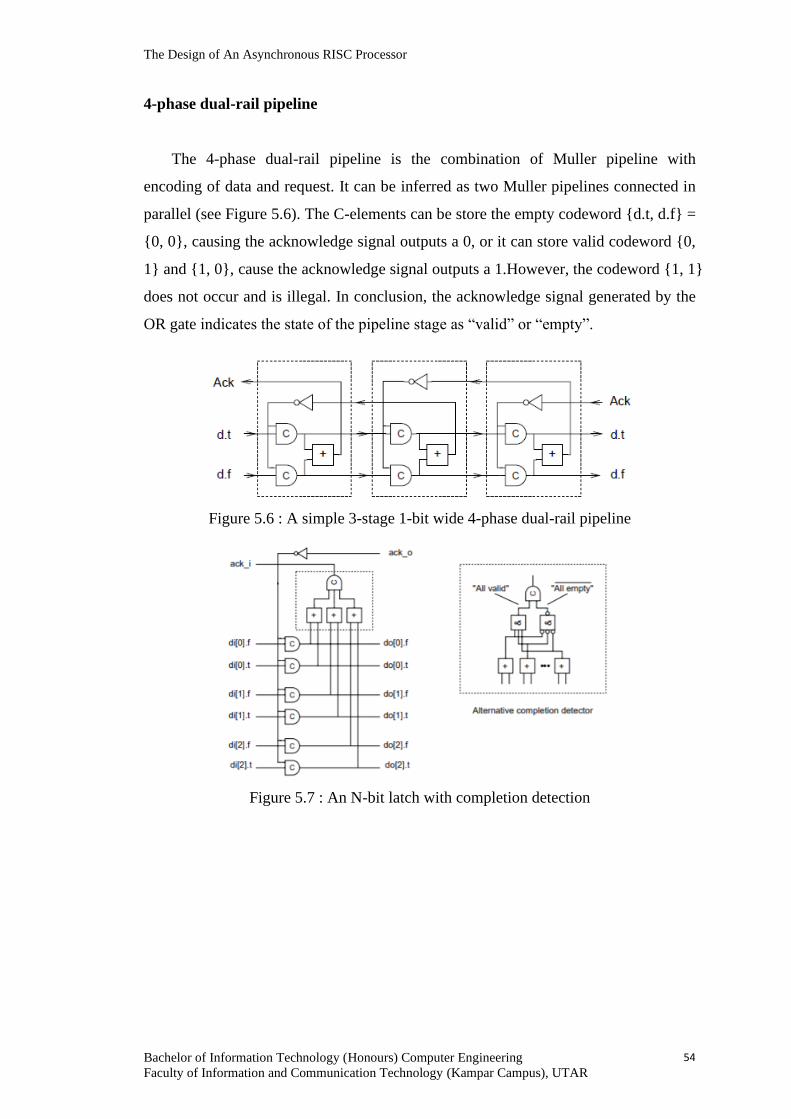
The Design of An Asynchronous RISC Processor
Bachelor of Information Technology (Honours) Computer Engineering
Faculty of Information and Communication Technology (Kampar Campus), UTAR
54
4-phase dual-rail pipeline
The 4-phase dual-rail pipeline is the combination of Muller pipeline with
encoding of data and request. It can be inferred as two Muller pipelines connected in
parallel (see Figure 5.6). The C-elements can be store the empty codeword {d.t, d.f} =
{0, 0}, causing the acknowledge signal outputs a 0, or it can store valid codeword {0,
1} and {1, 0}, cause the acknowledge signal outputs a 1.However, the codeword {1, 1}
does not occur and is illegal. In conclusion, the acknowledge signal generated by the
OR gate indicates the state of the pipeline stage as “valid” or “empty”.
Figure 5.6 : A simple 3-stage 1-bit wide 4-phase dual-rail pipeline
Figure 5.7 : An N-bit latch with completion detection
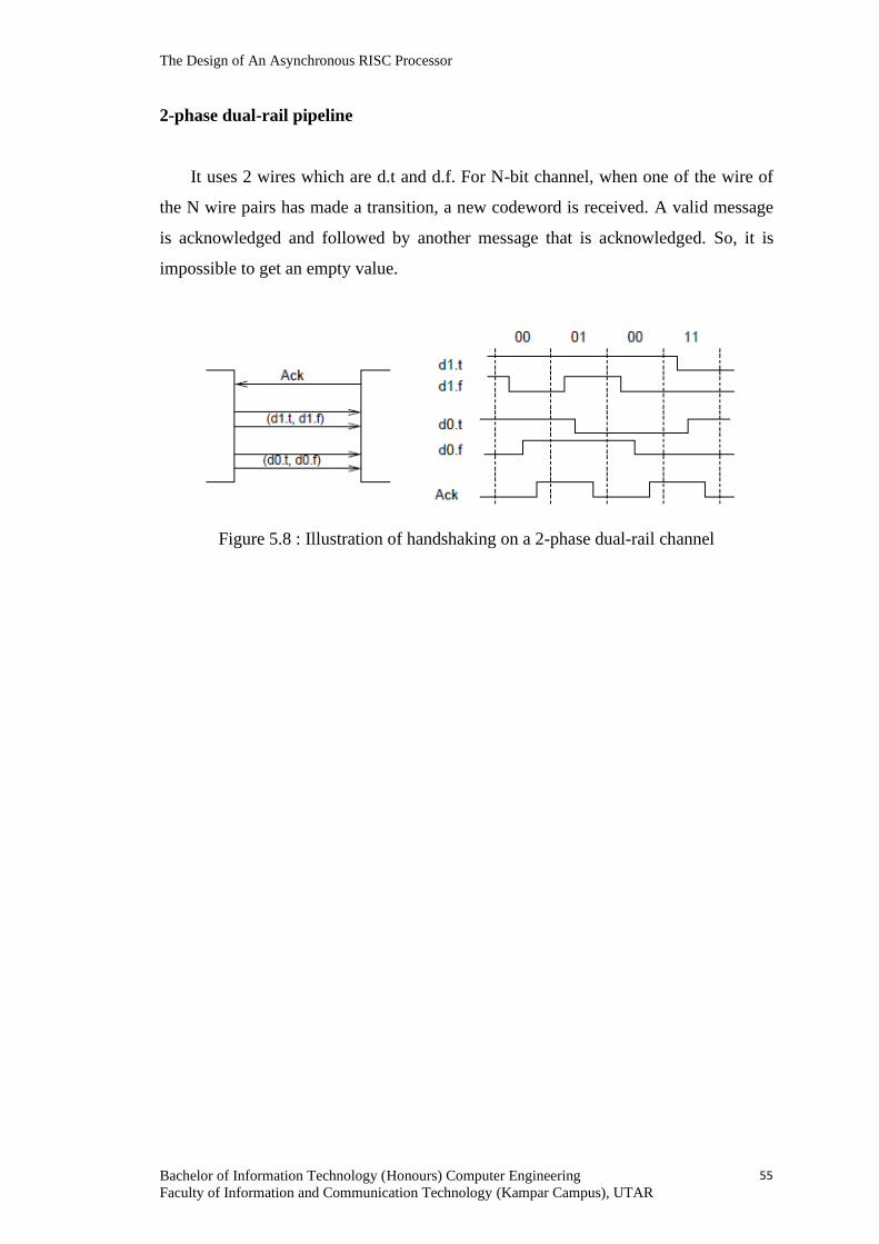
The Design of An Asynchronous RISC Processor
Bachelor of Information Technology (Honours) Computer Engineering
Faculty of Information and Communication Technology (Kampar Campus), UTAR
55
2-phase dual-rail pipeline
It uses 2 wires which are d.t and d.f. For N-bit channel, when one of the wire of
the N wire pairs has made a transition, a new codeword is received. A valid message
is acknowledged and followed by another message that is acknowledged. So, it is
impossible to get an empty value.
Figure 5.8 : Illustration of handshaking on a 2-phase dual-rail channel
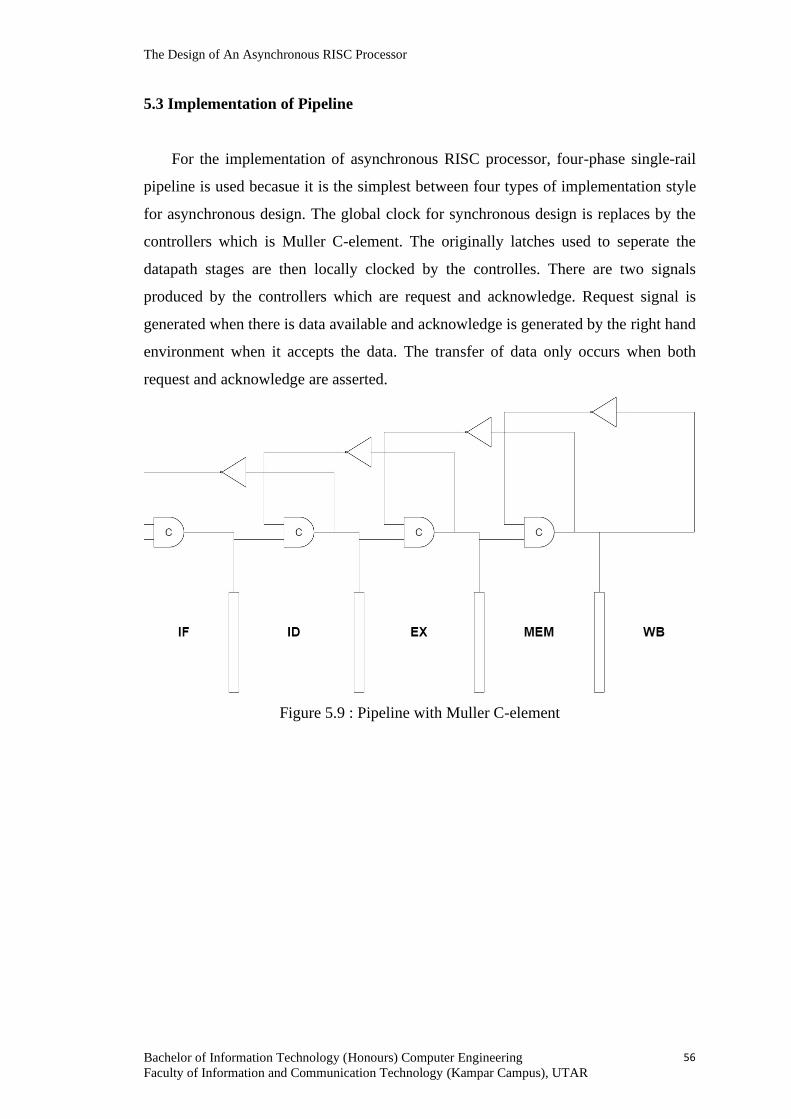
The Design of An Asynchronous RISC Processor
Bachelor of Information Technology (Honours) Computer Engineering
Faculty of Information and Communication Technology (Kampar Campus), UTAR
56
5.3 Implementation of Pipeline
For the implementation of asynchronous RISC processor, four-phase single-rail
pipeline is used becasue it is the simplest between four types of implementation style
for asynchronous design. The global clock for synchronous design is replaces by the
controllers which is Muller C-element. The originally latches used to seperate the
datapath stages are then locally clocked by the controlles. There are two signals
produced by the controllers which are request and acknowledge. Request signal is
generated when there is data available and acknowledge is generated by the right hand
environment when it accepts the data. The transfer of data only occurs when both
request and acknowledge are asserted.
Figure 5.9 : Pipeline with Muller C-element
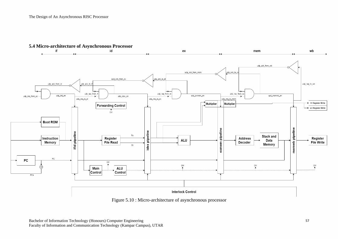
The Design of An Asynchronous RISC Processor
Bachelor of Information Technology (Honours) Computer Engineering
Faculty of Information and Communication Technology (Kampar Campus), UTAR
57
5.4 Micro-architecture of Asynchronous Processor
Figure 5.10 : Micro-architecture of asynchronous processor
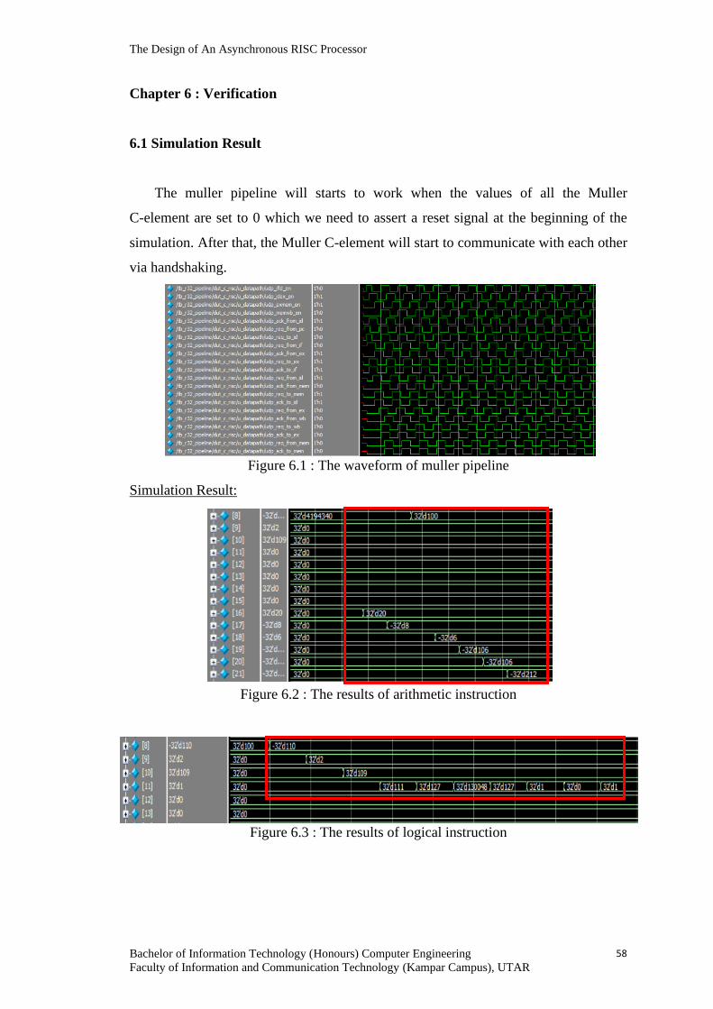
The Design of An Asynchronous RISC Processor
Bachelor of Information Technology (Honours) Computer Engineering
Faculty of Information and Communication Technology (Kampar Campus), UTAR
58
Chapter 6 : Verification
6.1 Simulation Result
The muller pipeline will starts to work when the values of all the Muller
C-element are set to 0 which we need to assert a reset signal at the beginning of the
simulation. After that, the Muller C-element will start to communicate with each other
via handshaking.
Figure 6.1 : The waveform of muller pipeline
Simulation Result:
Figure 6.2 : The results of arithmetic instruction
Figure 6.3 : The results of logical instruction
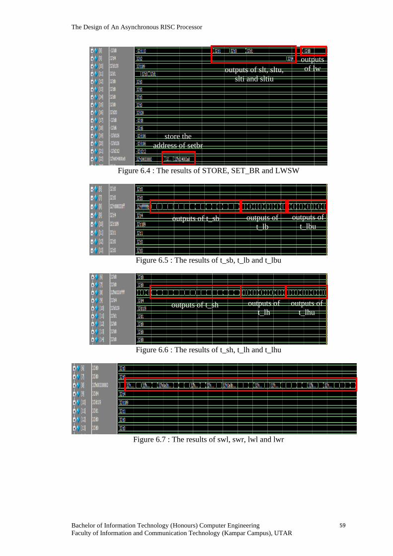
The Design of An Asynchronous RISC Processor
Bachelor of Information Technology (Honours) Computer Engineering
Faculty of Information and Communication Technology (Kampar Campus), UTAR
59
Figure 6.4 : The results of STORE, SET_BR and LWSW
Figure 6.5 : The results of t_sb, t_lb and t_lbu
Figure 6.6 : The results of t_sh, t_lh and t_lhu
Figure 6.7 : The results of swl, swr, lwl and lwr
store the
address of setbr
outputs of slt, sltu,
slti and sltiu
outputs
of lw
outputs of t_sb outputs of
t_lb
outputs of
t_lbu
outputs of t_sh outputs of
t_lh
outputs of
t_lhu
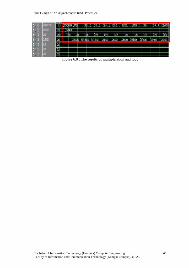
The Design of An Asynchronous RISC Processor
Bachelor of Information Technology (Honours) Computer Engineering
Faculty of Information and Communication Technology (Kampar Campus), UTAR
60
Figure 6.8 : The results of multiplication and loop
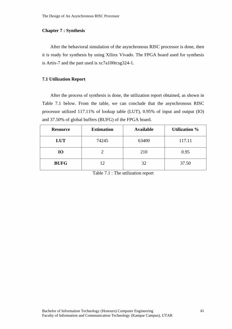
The Design of An Asynchronous RISC Processor
Bachelor of Information Technology (Honours) Computer Engineering
Faculty of Information and Communication Technology (Kampar Campus), UTAR
61
Chapter 7 : Synthesis
After the behavioral simulation of the asynchronous RISC processor is done, then
it is ready for synthesis by using Xilinx Vivado. The FPGA board used for synthesis
is Artix-7 and the part used is xc7a100tcsg324-1.
7.1 Utilization Report
After the process of synthesis is done, the utilization report obtained, as shown in
Table 7.1 below. From the table, we can conclude that the asynchronous RISC
processor utilized 117.11% of lookup table (LUT), 0.95% of input and output (IO)
and 37.50% of global buffers (BUFG) of the FPGA board.
Resource Estimation Available Utilization %
LUT 74245 63400 117.11
IO 2 210 0.95
BUFG 12 32 37.50
Table 7.1 : The utilization report
The Design of An Asynchronous RISC Processor
Bachelor of Information Technology (Honours) Computer Engineering
Faculty of Information and Communication Technology (Kampar Campus), UTAR
62
Chapter 8 : Conclusion and Future Work
8.1 Conclusion
The main objective of this project which is to design and synthesis the
asynchronous RISC processor has been achieved. The asynchronous RISC processor
is done by removing the global clock signal from synchronous processor and replaces
with the Muller C-element which has been discussed in Chapter 5. However. the
FPGA board, Artix-7 has been chosen to synthesis the asynchronous RISC processor
and the utilization report obtained after the synthesis is shown in Chapter 7. Moreover,
the behavioral of the asynchronous RISC processor has been verified correct without
errors. The simulation results are shown in Chapter 6.
8.2 Future Work
It is possible to do more advanced changes, but a good strategy is necessary to
have a performance gain. The programmable delays would be interesting to look into
so it will be possible to test what delays should be used on the different stages.
The Design of An Asynchronous RISC Processor
Bachelor of Information Technology (Honours) Computer Engineering
Faculty of Information and Communication Technology (Kampar Campus), UTAR
63
Bibliography
Mok K.M, 2008, Computer Organization and Architecture, lecture notes distributed in
Department of Computer and Communication Technology at Universiti Tunku Abdul
Rahman, 2008.
C.H. Van Berkel, M.B. Josephs & S.M. Nowick, 1999, Applications of Asynchronous
Circuits, Proceeding of the IEEE, vol. 87, no. 2, pp. 223-233.
Jens Sparsø & Steve, 2001, Principle of Asynchronous Circuit Design - A Systems
Perspective, Kluwer Academic Publishers.
Tony Werner & Venkatesh Akella, 1997, Asynchronous Processor Survey, IEEE, vol.
30, no. 11, pp. 67-76.
T.Samyuktha & K.Balachandra, 2015, Design and Performance Analysis of 8-Bit
Asynchronous Pipelined Processor. International Journal of Scientific Engineering
and Technology Research, vol. 4, no. 47, pp. 10206-10211.
Hans Jacobson, 1996, Asynchronous Circuit Design - A Case Study of A Framework
Called Ack, Master Thesis, Lulea University of Technology.
Bjørn Thomas Søreng Vee, 2014, Conversion of a simple Processor to asynchronous
Logic, Norwegian University of Science and Technology.
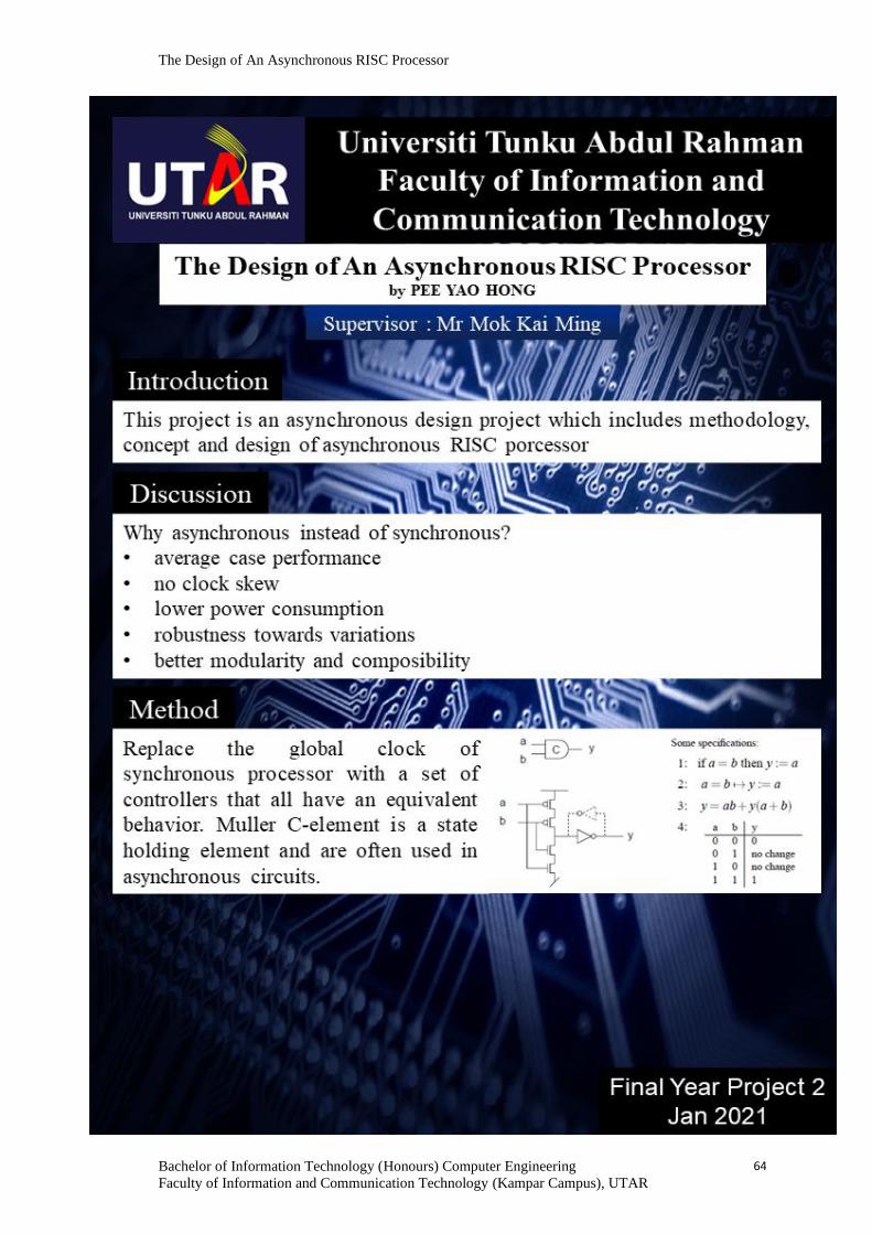
The Design of An Asynchronous RISC Processor
Bachelor of Information Technology (Honours) Computer Engineering
Faculty of Information and Communication Technology (Kampar Campus), UTAR
64
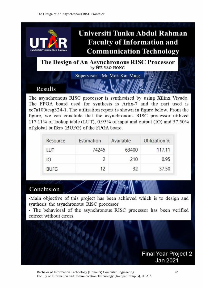
The Design of An Asynchronous RISC Processor
Bachelor of Information Technology (Honours) Computer Engineering
Faculty of Information and Communication Technology (Kampar Campus), UTAR
65
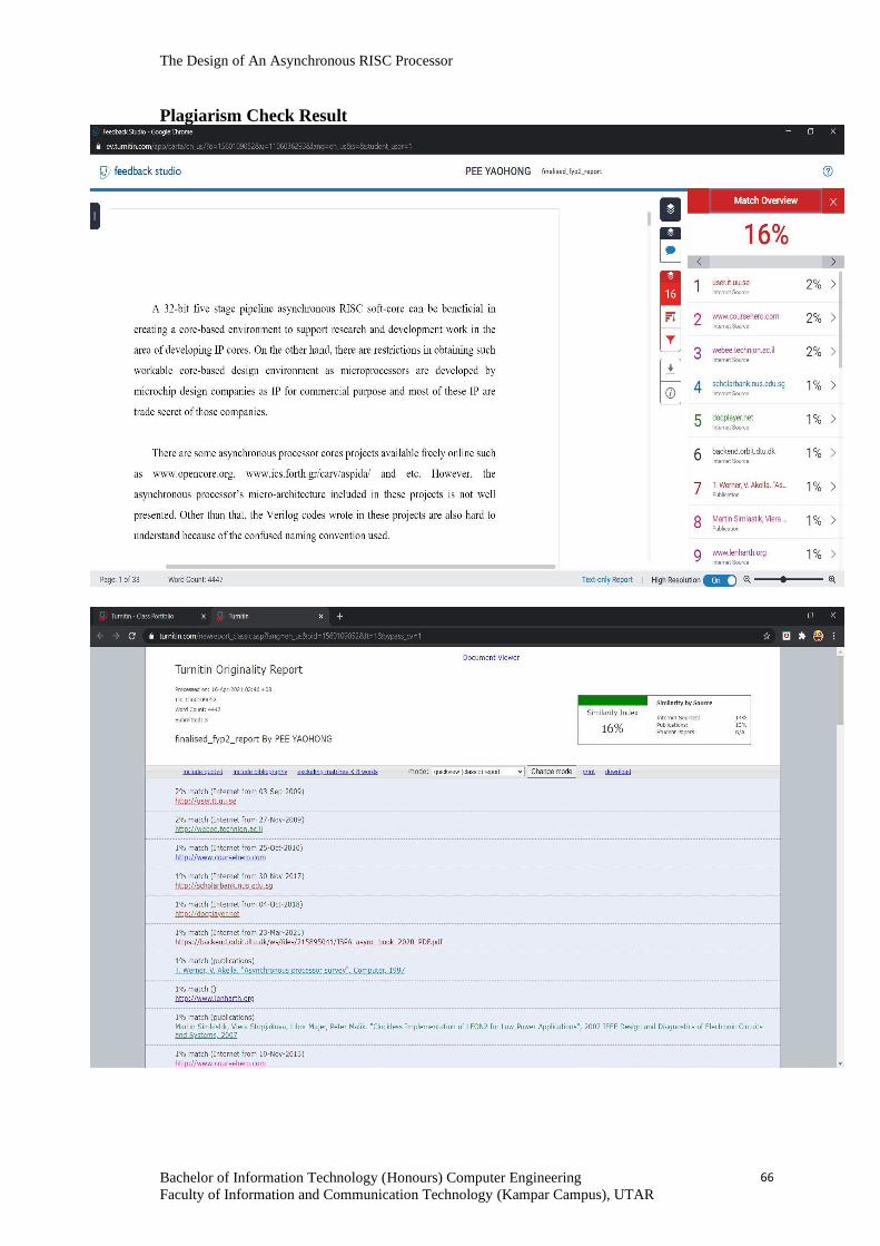
The Design of An Asynchronous RISC Processor
Bachelor of Information Technology (Honours) Computer Engineering
Faculty of Information and Communication Technology (Kampar Campus), UTAR
66
Plagiarism Check Result

The Design of An Asynchronous RISC Processor
Bachelor of Information Technology (Honours) Computer Engineering
Faculty of Information and Communication Technology (Kampar Campus), UTAR
67
FACULTY OF INFORMATION AND COMMUNICATION TECHNOLOGY
Full Name(s) of Candidate(s)
PEE YAO HONG
ID Number(s)
1802826
Programme / Course CT
Title of Final Year Project The Design of An Asynchronous RISC Processor
Similarity Supervisor’s Comments (Compulsory if parameters of originality exceeds the limits approved by UTAR)
Overall similarity index: 16% Similarity
by source Internet Sources: 14% Publications: 13% Student Papers: 0%
Number of individual sources listed of more than 3% similarity: NIL
Parameters of originality required and limits approved by UTAR are as Follows:
(i) Overall similarity index is 20% and below, and (ii) Matching of individual sources listed must be less than 3% each, and (iii) Matching texts in continuous block must not exceed 8 words
Note: Parameters (i) – (ii) shall exclude quotes, bibliography and text matches which are less than 8 words.
Note Supervisor/Candidate(s) is/are required to provide softcopy of full set of the
originality report to Faculty/Institute
Based on the above results, I hereby declare that I am satisfied with the originality of the
Final Year Project Report submitted by my student(s) as named above.
______________________________ ______________________________
Signature of Supervisor
Signature of Co-Supervisor
Name: __________________________
Name: __________________________
Date: ___________________________ Date: ___________________________
Universiti Tunku Abdul Rahman
Form Title : Supervisor’s Comments on Originality Report Generated by Turnitin
for Submission of Final Year Project Report (for Undergraduate Programmes)
Form Number: FM-IAD-005 Rev No.: 0 Effective Date: 01/10/2013 Page No.: 1of 1
MOK KAI MING
16/04/2021
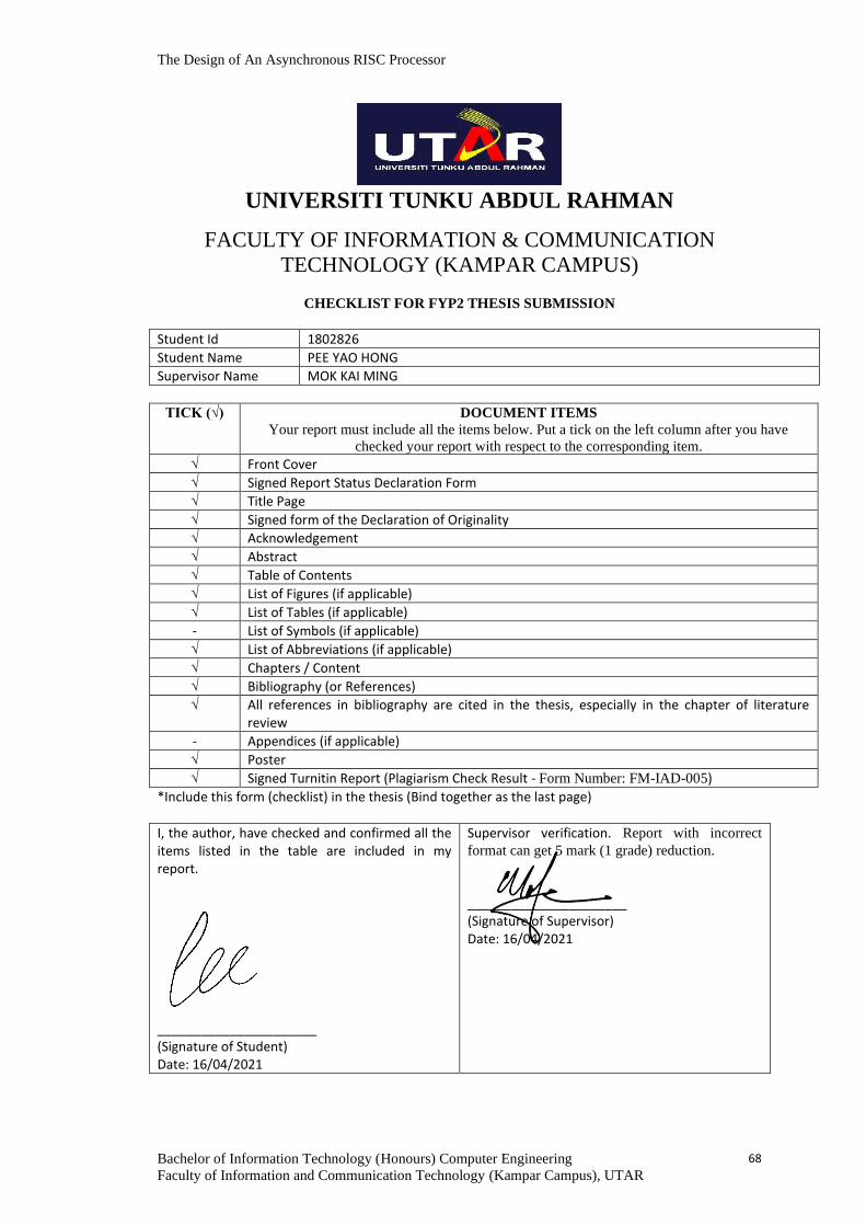
The Design of An Asynchronous RISC Processor
Bachelor of Information Technology (Honours) Computer Engineering
Faculty of Information and Communication Technology (Kampar Campus), UTAR
68
UNIVERSITI TUNKU ABDUL RAHMAN
FACULTY OF INFORMATION & COMMUNICATION
TECHNOLOGY (KAMPAR CAMPUS)
CHECKLIST FOR FYP2 THESIS SUBMISSION
Student Id 1802826
Student Name PEE YAO HONG
Supervisor Name MOK KAI MING
TICK (√) DOCUMENT ITEMS
Your report must include all the items below. Put a tick on the left column after you have
checked your report with respect to the corresponding item.
√ Front Cover
√ Signed Report Status Declaration Form
√ Title Page
√ Signed form of the Declaration of Originality
√ Acknowledgement
√ Abstract
√ Table of Contents
√ List of Figures (if applicable)
√ List of Tables (if applicable)
- List of Symbols (if applicable)
√ List of Abbreviations (if applicable)
√ Chapters / Content
√ Bibliography (or References)
√ All references in bibliography are cited in the thesis, especially in the chapter of literature review
- Appendices (if applicable)
√ Poster
√ Signed Turnitin Report (Plagiarism Check Result - Form Number: FM-IAD-005)
*Include this form (checklist) in the thesis (Bind together as the last page)
I, the author, have checked and confirmed all the items listed in the table are included in my report.
______________________ (Signature of Student) Date: 16/04/2021
Supervisor verification. Report with incorrect
format can get 5 mark (1 grade) reduction. ______________________ (Signature of Supervisor) Date: 16/04/2021