temperature-dependence on the structural, optical, and paramagnetic properties of zno nanostructures
TRANSCRIPT
Tp
GGa
0b
c
d
a
ARR1AA
KMZAOM
1
dc[[(cebpf
(
0h
Applied Surface Science 293 (2014) 62– 70
Contents lists available at ScienceDirect
Applied Surface Science
jou rn al h omepa g e: www.elsev ier .com/ locate /apsusc
emperature-dependence on the structural, optical, andaramagnetic properties of ZnO nanostructures
ugu H. Mhlongoa,∗, David E. Motaunga,∗∗, Steven S. Nkosib, H.C. Swartc,erald F. Malgasd, Kenneth T. Hilliea,c, Bonex W. Mwakikungaa
National Centre for Nano-structured Materials, Council for Scientific and Industrial Research, 1-Meiring Naude Road, Brummeria, PO Box 395, Pretoria00, South AfricaCSIR-National Laser Centre, 626 Meiring Naude Road, Brummeria, Pretoria 0001, South AfricaDepartment of Physics, University of the Free State, Bloemfontein ZA9300, South AfricaDepartment of Physics, University of the Western Cape, P/Bag X17, Bellville, South Africa
r t i c l e i n f o
rticle history:eceived 22 July 2013eceived in revised form3 December 2013ccepted 14 December 2013vailable online 22 December 2013
eywords:icrowave-assisted synthesis
nO nanostructuresnnealing effects
a b s t r a c t
Violet-blue emitting ZnO nanostructures were synthesized by a microwave-assisted hydrothermalmethod followed by post-synthesis annealing at different temperatures. Scanning electron microscopeanalysis revealed a morphological transformation upon increasing annealing temperature from well-defined “flower-like” structure composed of ZnO multi-nanorods to randomly oriented worm-like ZnOnanostructures. Raman analysis showed that the E2 (high) mode became sharper and stronger while theintensity of the phonon peak at 580 cm−1 was gradually enhanced with the increase of annealing tem-perature. X-ray diffraction and X-ray photoelectron spectroscopy (XPS) measurements showed that allZnO samples possess a typical wurtzite structure with high crystallinity and no other impurity phaseswere observed.
A decreasing trend in the photoluminescence (PL) intensity of a strong broad violet-blue emission
ptical propertiesagnetic propertiesfrom ZnO nanostructures with increasing annealing temperature was also observed. The electron spinresonance (ESR) signal was also found to gradually decrease with increasing annealing temperatureindicating the decrease in the concentration of zinc interstitials (Zni) and/or zinc vacancies (VZn) defectsin ZnO nanostructures. Moreover, a combination of results from the PL, XPS and ESR suggested that Znrelated defects; especially VZn and Zni are the primary source of the paramagnetism observed in the ZnOnanostructures.
. Introduction
ZnO has attracted a lot of research interest because of its wideirect band-gap of 3.37 eV, which is useful for a variety of appli-ations in light emitting diodes [1], gas sensors [2–4], solar cells5,6] photocatalytic agents [7] and other technological applications8]. ZnO has a larger exciton binding energy (60 meV) than GaN26 meV) and ZnSe (20 meV), respectively, which can ensure an effi-ient exciton emission at room temperature under low excitationnergy. Recently, the renewed interest in nanostructured ZnO has
een driven by its attractive prospects for applications in room tem-erature nanolasers [9], p-type doping [10], and room temperatureerromagnetic semiconductor nanomaterials [11]. These prospects∗ Corresponding author. Tel.: +27 12 841 3935; fax: +27 12 841 2229.∗∗ Corresponding author. Tel.: +27 12 841 4775; fax: +27 12 841 2229.
E-mail addresses: [email protected] (G.H. Mhlongo), [email protected]. Motaung).
169-4332/$ – see front matter © 2013 Elsevier B.V. All rights reserved.ttp://dx.doi.org/10.1016/j.apsusc.2013.12.076
© 2013 Elsevier B.V. All rights reserved.
have led to extensive studies on numerous aspects of ZnO nano-structures, including synthesis strategies, physical and chemicalproperties, and applications. However, some of the basic proper-ties of ZnO are not well understood [12,13] and are still debatableowing to the different intrinsic defects such as oxygen interstitials(Oi), zinc interstitials (Zni), oxygen vacancies (VO), zinc vacancies(VZn). At room temperature, ZnO typically exhibits one emissionpeak in the UV region due to the recombination of free excitonsand possibly one or more peaks in the visible spectral range whichare attributed to defect emissions, but the origin of defect emissionsis still unclear. For the most commonly observed green defect emis-sion [14–19], various hypotheses have been proposed such as tran-sition between singly ionized VO and photo-excited holes [20,21],transition between electrons close to the conduction band anddeeply trapped holes at VO [19,22]. The orange-red emission is also
commonly attributed to the presence of excess oxygen in the sam-ples [17,23] such as Oi defects [19,22,24]. The violet-blue emissionhas been previously attributed to electronic transitions from Znito valence band and transitions between VO and Oi [25,26]. Other
G.H. Mhlongo et al. / Applied Surface Science 293 (2014) 62– 70 63
7060504030200
100000
200000
300000
400000
500000
600000
700000
800000
Inte
nsity
[a.u
]
112
112
200
10311
0
102
101
002
100
2 theta [degrees]
as prepared200 oC600 oC900 oC
(a)
1000800600400200025
30
35
40
Calcination temperature [oC]
Cry
stal
lite
size
[nm
]
0.0040
0.0045
0.0050
0.0055
FWH
M of (101) peak
(b)
F ifferes
rsoitdtescodbat
2
zT1a
ig. 1. (a) The XRD patterns of the ZnO nanostructures before and after annealing at dize of the ZnO nanostructures depending on annealing temperature.
esearchers attributed this emission to related intrinsic defectsuch as VO and VZn or interstitials and their complexes [24,27]. It isbvious based on these reports that the origin of defect emissionsn ZnO is still an unresolved issue. The proposed explanations forhe different visible emissions in ZnO are often contradictory, withifferent defect types proposed to explain the same emission orhe same defect types proposed to explain emission in the differ-nt spectral ranges. Therefore, considerable interest is still beinghown in exploring the ZnO nanostructures as magnetic semi-onductors. In this paper, we report on a hydrothermal synthesisf one-dimensional ZnO nanostructures followed by annealing atifferent temperatures. The origin of defects responsible for violet-lue emissions in ZnO nanostructures has been investigated by theid of electron spin resonance (ESR), X-ray photo-electron spec-roscopy (XPS), and photoluminescence (PL).
. Experimental
ZnO nanostructures were prepared from aqueous solutions of
inc acetate (Zn(CH3COO)2·2H2O) and hydrazine hydrate (N2H4).hese precursor solutions were mixed in a molar ratio of 1:4 in00 ml of distilled water under vigorous stirring. N2H4 solution wasdded drop-wise into zinc acetate solution and it slowly reactednt temperatures. (b) The FWHM of (1 0 1) diffraction peaks and estimated crystallite
with zinc acetate resulting in a formation of slurry-like precipitate.The solution was continuously stirred for 15 min, then trans-ferred in a 100 ml Teflon liner and finally subjected to microwave(Perkin Elmer/Anton Paar Multiwave 3000) oven irradiation at amicrowave power of 150 W for 10 min. The resulting white pre-cipitate at the bottom was collected, then filtered off and thenwashed several times with absolute ethanol and distilled water toremove any impurities. For preparation of ZnO nanostructures, theremaining powder was then dried in air for 2 h at 90 ◦C. Anneal-ing in air was also performed at different temperatures from 200 to900 ◦C for 2 h. All the chemicals were purchased from Sigma Aldrichand used as received without further purification.
The samples structure was analyzed by X-ray diffraction (XRD)(PANalytical Xpert PRO) using the Cu K� radiation source. Themorphologies were observed from the JEOL JSM-7500F, field emis-sion scanning electron microscopy (FE-SEM). Optical propertieswere characterized using room temperature UV-VIS absorption(Perkin-Elmer Lamda 750S UV-VIS) and PL (Jobin-Yvon NanoLogspectrometer) at an excitation wavelength of 325 nm. X-ray photo-
electron spectroscopy (XPS) analyses were carried using a PHI5000 Versaprobe-Scanning ESCA Microprobe. A low energy Ar+ iongun and low energy neutralizer electron gun were used to min-imize charging on the surface. Monochromatic Al K� radiation
64 G.H. Mhlongo et al. / Applied Surface Science 293 (2014) 62– 70
nneal
(eet(ugaTTsTHt0oJtpafir
3
t6wtpptdpaot
gap due to some defects or impurities present in the ZnO lattice
Fig. 2. FE-SEM images of ZnO nanostructures (a) before and after a
h� = 1486.6 eV) was used as the excitation source. A 25 W, 15 kVlectron beam was used to excite the X-ray beam of 100 �m diam-ter that was used for the analyses. For the higher resolution spectrahe hemispherical analyser pass energy was maintained at 11.8 eVC 1s, O 1s, and Zn 2p) for 50 cycles. Measurements were performedsing either a 1 eV/step and 45 min acquisition time (binding ener-ies ranging from 0 to 1400 eV) for survey scans or a 0.1 eV/stepnd 20–30 min acquisition times for the high resolution scans.he pressure during acquisition was typically below 1 × 10⁻⁸ Torr.he same measurements were repeated after the surfaces wereputtered clean for 30 s using an Ar+ ion gun (2 kV energy ions).he Raman spectroscopy measurements were conducted using aoriba Jobin-Yvon HR800 Raman microscope at room tempera-
ure with a 514 nm excitation laser with a spectral resolution of.4 cm−1. The microwave absorption measurements were carriedut using JEOL X-band electron spin resonance (ESR) spectrometerES FA 200 equipped with an Oxford ESR900 gas-flow cryostat and aemperature control (Scientific instruments 9700). The microwaveower was kept constant at 30 (5) mW while the frequency wasbout 9.4 GHz. The DC field was modulated with a superposed aceld whose amplitude was maintained constant. The microwaveesponse was measured as a derivative signal.
. Results and discussions
Fig. 1(a) shows the XRD diffraction patterns of ZnO nanostruc-ures before and after annealing at different temperatures (200,00 and 900 ◦C). All the diffraction patterns correspond to theurtzite structure (hexagonal phase) of ZnO. No additional diffrac-
ion peaks due to impurities were detected. The crystallographichases were identified by comparison with the XRD patterns ofure ZnO JCPDS card No. 79-2205 database. The preferred orienta-ion corresponding to the (1 0 1) plane was the most prominentiffraction peak. It was also noted that the primary diffractioneaks became stronger and sharper after the annealing temper-
ture was increased up to 900 ◦C indicating improved crystallinityf the ZnO nanostructures. By using the Debye–Scherrer’s equa-ion, the full width at half-maximum (FWHM) of the most intenseing at different temperatures (b) 200 ◦C, (c) 600 ◦C, and (d) 900 ◦C.
diffraction peak (1 0 1) and the average crystallite size were esti-mated and the results are shown in Fig. 1(b). It can be seen fromthe plot that, the increase of annealing temperature led to thedecrease of the FWHM of the (1 0 1) diffraction peaks while theaverage crystallite size is increased. However, for the ZnO sam-ple annealed at 600 ◦C, a slight increase and decrease in FWHM ofthe (1 0 1) diffraction peak and average crystallite size was noted,respectively. The decrease of the FWHM with increasing annealingtemperature could be due to the coalescences of grains at highertemperatures thus leading to increase in the average crystallitesize due to improvement of crystallinity of ZnO nanostructures[28].
The FE-SEM images presented in Fig. 2 show the morpholog-ical change of ZnO nanostructures before and after annealing atdifferent temperatures. It can be seen from Fig. 2(a) that priorto annealing; the ZnO nanostructures consisted of a bunch ofmulti-nanorods originating from one nucleating centre to form“flower-like” structures. A slight increase in annealing temperatureto 200 ◦C resulted in the formation of a hexagonal structure witha smooth surface at the bottom of each bunch of multi-nanorods,Fig. 2(b). At 600 ◦C, these multi-nanorods were clustered togetherand then deviated into cones as shown in Fig. 2(c). However, it wasalso noticed that with a further increase of annealing temperatureup to 900 ◦C (Fig. 2(d)), the structures were made-up of small ringspacking up together towards the end of the tip, having the shape ofa worm with smooth surface.
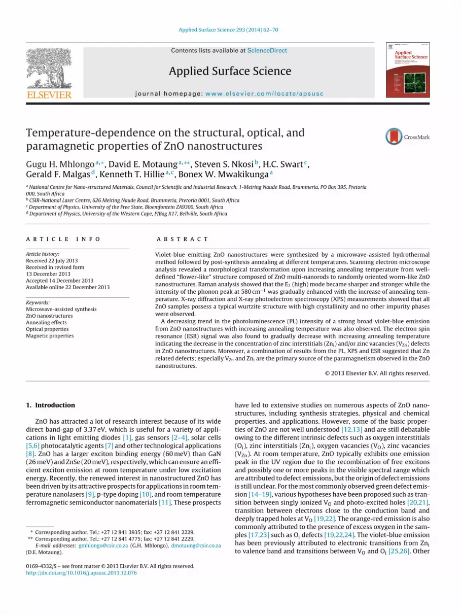
Fig. 3 shows the optical absorption spectra of the as preparedand annealed ZnO nanostructures at different temperatures. Theabsorption spectra revealed absorption peaks around 378 nm, cor-responding to the as-prepared ZnO sample. When annealing thesamples to 200 ◦C and higher temperatures an obvious red-shiftin the absorption edge was observed. This red-shift might be dueto changes in the ZnO nanostructures’ morphologies and surfacemicrostructure. Also, the presence of shallow levels inside the band
cannot be excluded as one of the possible causes of progressivered-shift observed with an increasing temperature on the ZnOnanostructures in this case.
G.H. Mhlongo et al. / Applied Surface Science 293 (2014) 62– 70 65
Fa
RacpopalnFatn3mwbtt[tt
Ft
ig. 3. UV–vis absorption spectra of ZnO nanostructures for as-prepared andnnealed at 200, 600, and 900 ◦C.
To study the vibrational modes of the ZnO nanostructures,aman scattering measurements were performed at room temper-ture. According to the group theory predictions, the Raman-activeentre modes of ZnO are A1 + 2E2 + E1, where A1 and E1 are polarhonons and, hence, exhibit different frequencies for the transverseptical (TO) and longitudinal-optical (LO) phonons. Non-polarhonon modes with symmetry E2 have two frequencies: E2 (high)ssociated with oxygen atoms and E2 (low) associated with Zn sub-attice [29]. Fig. 4 depicts the Raman-scattering spectra of the ZnOanostructures prior and after annealing at different temperatures.or all spectra, the sharp, strong and dominant peak located atbout 438 cm−1 believed to be a characteristic scattering peak ofhe Raman-active dominant E2 (high) mode of wurtzite hexago-al ZnO was observed [30,31]. In addition, two peaks at 330 and70 cm−1 which can be assigned to E2H–E2L (multi-phonon) A1 (TO)odes were also observed, respectively [22,32]. A broadened andeak peak at 580 cm−1 also appeared in all spectra. Normally, in
ulk ZnO, the frequency 574 cm−1 of 1LO phonon peak correspondso A1 (LO) phonon and it can only be observed in the configura-
ion when the c-axis of wurtzite ZnO is parallel to the sample face30]. However, if the c-axis is perpendicular to the sample face,he E1 (LO) (591 cm−1) phonon is observed, instead [29]. Based onhe theory of polar optical phonons in wurtzite nanocrystals [32],ig. 4. Raman spectra of ZnO nanostructures prior and after annealing at differentemperatures: 200, 600, and 900 ◦C.
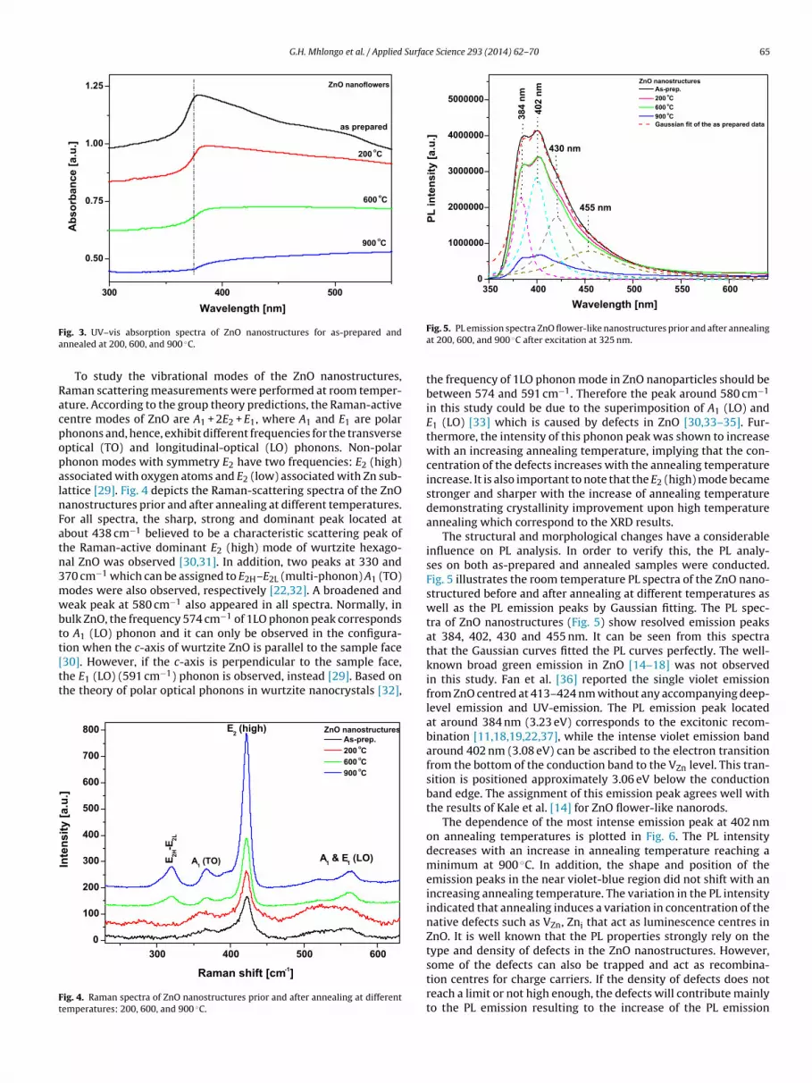
Fig. 5. PL emission spectra ZnO flower-like nanostructures prior and after annealingat 200, 600, and 900 ◦C after excitation at 325 nm.
the frequency of 1LO phonon mode in ZnO nanoparticles should bebetween 574 and 591 cm−1. Therefore the peak around 580 cm−1
in this study could be due to the superimposition of A1 (LO) andE1 (LO) [33] which is caused by defects in ZnO [30,33–35]. Fur-thermore, the intensity of this phonon peak was shown to increasewith an increasing annealing temperature, implying that the con-centration of the defects increases with the annealing temperatureincrease. It is also important to note that the E2 (high) mode becamestronger and sharper with the increase of annealing temperaturedemonstrating crystallinity improvement upon high temperatureannealing which correspond to the XRD results.
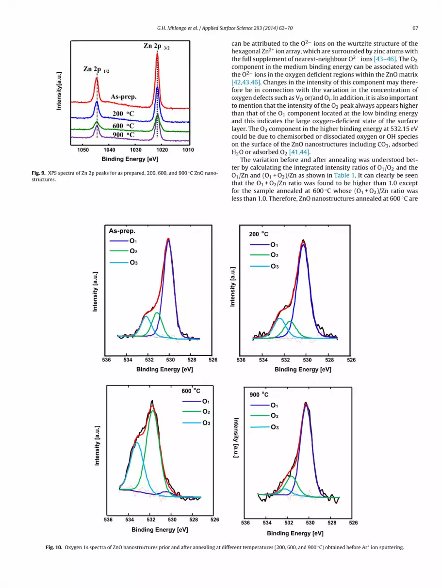
The structural and morphological changes have a considerableinfluence on PL analysis. In order to verify this, the PL analy-ses on both as-prepared and annealed samples were conducted.Fig. 5 illustrates the room temperature PL spectra of the ZnO nano-structured before and after annealing at different temperatures aswell as the PL emission peaks by Gaussian fitting. The PL spec-tra of ZnO nanostructures (Fig. 5) show resolved emission peaksat 384, 402, 430 and 455 nm. It can be seen from this spectrathat the Gaussian curves fitted the PL curves perfectly. The well-known broad green emission in ZnO [14–18] was not observedin this study. Fan et al. [36] reported the single violet emissionfrom ZnO centred at 413–424 nm without any accompanying deep-level emission and UV-emission. The PL emission peak locatedat around 384 nm (3.23 eV) corresponds to the excitonic recom-bination [11,18,19,22,37], while the intense violet emission bandaround 402 nm (3.08 eV) can be ascribed to the electron transitionfrom the bottom of the conduction band to the VZn level. This tran-sition is positioned approximately 3.06 eV below the conductionband edge. The assignment of this emission peak agrees well withthe results of Kale et al. [14] for ZnO flower-like nanorods.
The dependence of the most intense emission peak at 402 nmon annealing temperatures is plotted in Fig. 6. The PL intensitydecreases with an increase in annealing temperature reaching aminimum at 900 ◦C. In addition, the shape and position of theemission peaks in the near violet-blue region did not shift with anincreasing annealing temperature. The variation in the PL intensityindicated that annealing induces a variation in concentration of thenative defects such as VZn, Zni that act as luminescence centres inZnO. It is well known that the PL properties strongly rely on thetype and density of defects in the ZnO nanostructures. However,some of the defects can also be trapped and act as recombina-
tion centres for charge carriers. If the density of defects does notreach a limit or not high enough, the defects will contribute mainlyto the PL emission resulting to the increase of the PL emission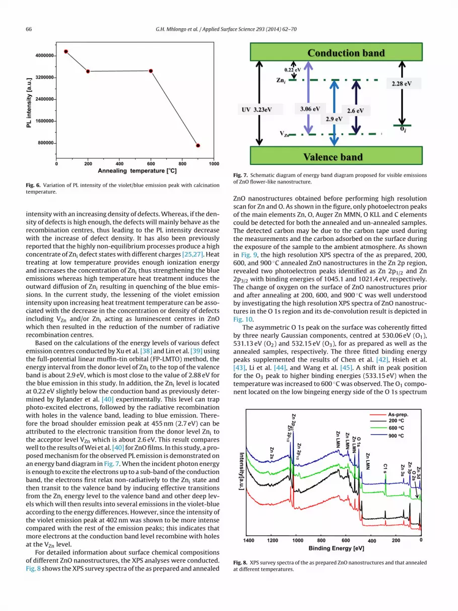
66 G.H. Mhlongo et al. / Applied Surface Science 293 (2014) 62– 70
10008006004002000
800000
1600000
2400000
3200000
4000000
PL in
tens
ity [a
.u.]
Annealing temperature [oC]
Ft
isrwrctaeosiciwr
etebtampwfatwpaibtfeatcma
oF
[43], Li et al. [44], and Wang et al. [45]. A shift in peak positionfor the O3 peak to higher binding energies (533.15 eV) when thetemperature was increased to 600 ◦C was observed. The O1 compo-nent located on the low bingeing energy side of the O 1s spectrum
Zn 2p1/2
600800100012001400 400 200 0
Intensity[a.u.]
Zn 2p3/2 Zn LM
N
Zn 3p
Zn LMN
O 1sZn 2p
1/2
Zn LMNZn 2s
C1 s
Zn 3s
Zn 3d
Zn LMN
O 2s
As-prep.200 oC600 oC900 oC
ig. 6. Variation of PL intensity of the violet/blue emission peak with calcinationemperature.
ntensity with an increasing density of defects. Whereas, if the den-ity of defects is high enough, the defects will mainly behave as theecombination centres, thus leading to the PL intensity decreaseith the increase of defect density. It has also been previously
eported that the highly non-equilibrium processes produce a highoncentrate of Zni defect states with different charges [25,27]. Heatreating at low temperature provides enough ionization energynd increases the concentration of Zni thus strengthening the bluemissions whereas high temperature heat treatment induces theutward diffusion of Zni resulting in quenching of the blue emis-ions. In the current study, the lessening of the violet emissionntensity upon increasing heat treatment temperature can be asso-iated with the decrease in the concentration or density of defectsncluding VZn and/or Zni acting as luminescent centres in ZnO
hich then resulted in the reduction of the number of radiativeecombination centres.
Based on the calculations of the energy levels of various defectmission centres conducted by Xu et al. [38] and Lin et al. [39] usinghe full-potential linear muffin-tin orbital (FP-LMTO) method, thenergy interval from the donor level of Zni to the top of the valenceand is about 2.9 eV, which is most close to the value of 2.88 eV forhe blue emission in this study. In addition, the Zni level is locatedt 0.22 eV slightly below the conduction band as previously deter-ined by Bylander et al. [40] experimentally. This level can trap
hoto-excited electrons, followed by the radiative recombinationith holes in the valence band, leading to blue emission. There-
ore the broad shoulder emission peak at 455 nm (2.7 eV) can bettributed to the electronic transition from the donor level Zni tohe acceptor level VZn which is about 2.6 eV. This result comparesell to the results of Wei et al. [40] for ZnO films. In this study, a pro-osed mechanism for the observed PL emission is demonstrated onn energy band diagram in Fig. 7. When the incident photon energys enough to excite the electrons up to a sub-band of the conductionand, the electrons first relax non-radiatively to the Zni state andhen transit to the valence band by inducing effective transitionsrom the Zni energy level to the valence band and other deep lev-ls which will then results into several emissions in the violet-blueccording to the energy differences. However, since the intensity ofhe violet emission peak at 402 nm was shown to be more intenseompared with the rest of the emission peaks; this indicates thatore electrons at the conduction band level recombine with holes
t the V level.
ZnFor detailed information about surface chemical compositionsf different ZnO nanostructures, the XPS analyses were conducted.ig. 8 shows the XPS survey spectra of the as prepared and annealed
Fig. 7. Schematic diagram of energy band diagram proposed for visible emissionsof ZnO flower-like nanostructure.
ZnO nanostructures obtained before performing high resolutionscan for Zn and O. As shown in the figure, only photoelectron peaksof the main elements Zn, O, Auger Zn MMN, O KLL and C elementscould be detected for both the annealed and un-annealed samples.The detected carbon may be due to the carbon tape used duringthe measurements and the carbon adsorbed on the surface duringthe exposure of the sample to the ambient atmosphere. As shownin Fig. 9, the high resolution XPS spectra of the as prepared, 200,600, and 900 ◦C annealed ZnO nanostructures in the Zn 2p region,revealed two photoelectron peaks identified as Zn 2p1/2 and Zn2p3/2 with binding energies of 1045.1 and 1021.4 eV, respectively.The change of oxygen on the surface of ZnO nanostructures priorand after annealing at 200, 600, and 900 ◦C was well understoodby investigating the high resolution XPS spectra of ZnO nanostruc-tures in the O 1s region and its de-convolution result is depicted inFig. 10.
The asymmetric O 1s peak on the surface was coherently fittedby three nearly Gaussian components, centred at 530.06 eV (O1),531.13 eV (O2) and 532.15 eV (O3), for as prepared as well as theannealed samples, respectively. The three fitted binding energypeaks supplemented the results of Chen et al. [42], Hsieh et al.
Binding Energy [eV]
Fig. 8. XPS survey spectra of the as prepared ZnO nanostructures and that annealedat different temperatures.
G.H. Mhlongo et al. / Applied Surfac
Zn 2p 3/2
Zn 2p 1/2
As-prep.
10101020103010401050
Binding Energy [eV]
Inte
nsity
[a.u
.]
200 oC
600 oC900 oC
Fig. 9. XPS spectra of Zn 2p peaks for as prepared, 200, 600, and 900 ◦C ZnO nano-s
tructures.526528530532534536
Binding Energy [eV]
Inte
nsity
[a.u
.]
600 oC
O1
O2
O3
526528530532534536
Binding Energy [eV]
Inte
nsity
[a.u
.]
As-prep.O1
O2
O3
Fig. 10. Oxygen 1s spectra of ZnO nanostructures prior and after annealing at diffe
e Science 293 (2014) 62– 70 67
can be attributed to the O2− ions on the wurtzite structure of thehexagonal Zn2+ ion array, which are surrounded by zinc atoms withthe full supplement of nearest-neighbour O2− ions [43–46]. The O2component in the medium binding energy can be associated withthe O2− ions in the oxygen deficient regions within the ZnO matrix[42,43,46]. Changes in the intensity of this component may there-fore be in connection with the variation in the concentration ofoxygen defects such as VO or/and Oi. In addition, it is also importantto mention that the intensity of the O2 peak always appears higherthan that of the O1 component located at the low binding energyand this indicates the large oxygen-deficient state of the surfacelayer. The O3 component in the higher binding energy at 532.15 eVcould be due to chemisorbed or dissociated oxygen or OH specieson the surface of the ZnO nanostructures including CO3, adsorbedH2O or adsorbed O2 [41,44].
The variation before and after annealing was understood bet-ter by calculating the integrated intensity ratios of O1/O2 and theO /Zn and (O + O )/Zn as shown in Table 1. It can clearly be seen
1 1 2that the O1 + O2/Zn ratio was found to be higher than 1.0 exceptfor the sample annealed at 600 ◦C whose (O1 + O2)/Zn ratio wasless than 1.0. Therefore, ZnO nanostructures annealed at 600 ◦C are526528530532534536
Binding Energy [eV]
Inte
nsity
[a.u
.]200 oC
O1
O2
O3
526528530532534536
Binding Energy [eV]
Intensity [a.u.]
900 oC
O1
O2
O3
rent temperatures (200, 600, and 900 ◦C) obtained before Ar+ ion sputtering.

68 G.H. Mhlongo et al. / Applied Surface Science 293 (2014) 62– 70
Table 1XPS data of O and atom ratio of Zn to oxygen on the surface of the Zn nanostructures annealed at different temperature.
Annealingtemperature (◦C)
O1 position (eV) O2 position (eV) O3 position (eV) Intensity of O1 (%) Intensity of O2 (%) Intensity of O3 (%) O1/O2 O1/Zn O1 + O2/Zn
As-prep. 530.06 531.13 532.15 68.31 17.02 14.67 4.01 1.03 1.29200 530.26 531.47 532.39 69.94 13.50 16.55 5.18 1.05 1.26
4
7
ooZorwwaeiattpctprscatcfaoawd
eitiZpttbmffbaoafto
dfr2da
nificant at room temperature (298 K) and it disappears completelywith annealing temperature. The disappearance of the LFMA sig-nal in the ZnO nanostructure above room temperature is in good
600 530.41 531.69 533.19 3.6900 530.26 531.61 532.26 76.8
xygen-deficient while the rest of the samples contain excessxygen. A similar behaviour was noticed for the O1/Zn ratio fornO nanostructures annealed at 600 ◦C indicating that most of thexygen ions are not in the stoichiometric Zn O bonding. This cor-esponds to the drastic drop in the intensity of the O1 peak whichas observed after annealing at 600 ◦C. The strong Zn O bondingas observed for un-annealed samples and those annealed at 200
nd 900 ◦C as the intensity of their O1 component was shown toxceed that of the O2 and O3 components. On the other hand, thentensity of the O2 peak showed an increase with increasing thennealing temperature up to 600 ◦C and a significant drop with fur-her increase in annealing temperature up to 900 ◦C. The increase inhe intensity of this component with an increase in annealing tem-erature up to 600 ◦C can be associated with the increase in theoncentration of defects on the surface of ZnO and this is believedo be due to thermal diffusion which normally occurs at high tem-eratures. The drop in the intensity of this peak at 900 ◦C may beelated to elimination of some defects on the surface of ZnO nano-tructures. For the O3 component, it was noticed that the intensityontinuously increases when increasing temperature up to 600 ◦Cnd thereafter drastically decrease when increasing the annealingemperature up to 900 ◦C. This clearly indicates that the chemi-al adsorption of the surface of the ZnO nanostructures is higheror the samples annealed at 600 ◦C as compared to those annealedt 200 and 900 ◦C. According to the XPS results there was excessxygen present in all the ZnO nanostructures except for the 600 ◦Cnnealed sample. However, the variation of the (O1 + O2)/Zn ratioith increasing temperature suggests the involvement of otherefects related to Zn such as VZn and Zni as confirmed by PL analysis.
In general, it is believed that the intensity ratio of UV- to visiblemission is considered as an indication of excellent crystal qual-ty and low defect concentration. It is known that higher annealingemperatures reduce the trap states in a material, thus improv-ng the crystallinity. In the current study, the crystallinity of thenO nanostructures increases with an increase in annealing tem-erature up to 900 ◦C. This suggests that the crystal quality ofhe as-prepared or samples annealed at 200 ◦C or 600 ◦C is rela-ively poor compared to those annealed at 900 ◦C. Therefore it iselieved that annealing temperatures lower than 900 ◦C inducesore defects than those annealed at 900 ◦C. A possible explanation
or this may be that the non-radiative defect concentration is loweror samples annealed below 900 ◦C hence the samples annealedelow 900 ◦C exhibited higher PL and UV–vis relative intensitiess compared to that annealed at 900 ◦C. A similar trend is alsobserved on the EPR signal (see Fig. 11) as it reduces with increasingnnealing temperature. Also significant change in microstructuraleatures evolved at different temperatures and this has led to varia-ion both in the optical absorption and luminescent characteristicsf the samples.
In order to further understand the presence of paramagneticefects in ZnO nanostructures, the ESR measurements were per-ormed at room temperature. The comparison between the ESR
esponses from ZnO nanostructures prior and after annealing at00, 600, and 900 ◦C were conducted. Fig. 11 shows the first orderifferential ESR spectra of the ZnO nanostructures before andfter annealing at different temperatures. The low-field microwave59.91 36.45 0.06 0.05 0.9617.60 5.53 4.36 1.16 1.43
absorption (LFMA) process which usually originates from the mag-netization processes far from the saturation state also supported bybulk magnetization is observed for the as-prepared ZnO nanostruc-tures. The LFMA signal is opposite in phase with respect to that ofparamagnetic resonance (PMR). This indicates that the LFMA hasmicrowave absorption minimum at zero fields in contrast to themicrowave absorption maximum for the PMR line at its resonancefield. LFMA is understood to be connected to the magnetization pro-cesses that occur at applied low field. It is therefore assumed thatmagnetization processes is present at HDC = 0 and such magnetiza-tion process is attributed to the interaction of magnetic momentsof the ZnO with the magnetic-field component of electromagneticradiation. It is interesting to note that the LFMA spectra are only sig-
Fig. 11. ESR spectra of the as prepared and annealed (200, 600, and 900 ◦C) ZnOnanostructures.
G.H. Mhlongo et al. / Applied Surface Science 293 (2014) 62– 70 69
Table 2Lande ‘g’ factor, line width (�H) and number of spins (Nspins) of ZnO nanostructures.
Annealing temperature (◦C) FMR field (mT) g-Factor �HEPR (mT) No. of spins, Nspins (×104) Crystallite size (nm)
As-prep. 327.67 1.955 3.41 3.26 26.4200 328.12 1.945 4.12 2.28 28.9
3.11 2.32 27.82.89 0.27 38.8
atssawmrbaitcfaiZZtbsdiaEHiTtbmmndtlPittwofanpi
ott(fstit
1000800600400200010-1
102
105
109
1010
R = -0.85
R = -0.85
R = +0.98
R = +0.82
R = +0.02
Inte
nsity
(a.u
.)Annealing Temperature (oC)
spin populationcrystallite size (nm)O/Zn ratioabsorption edge (nm)violet-blue PL intensity
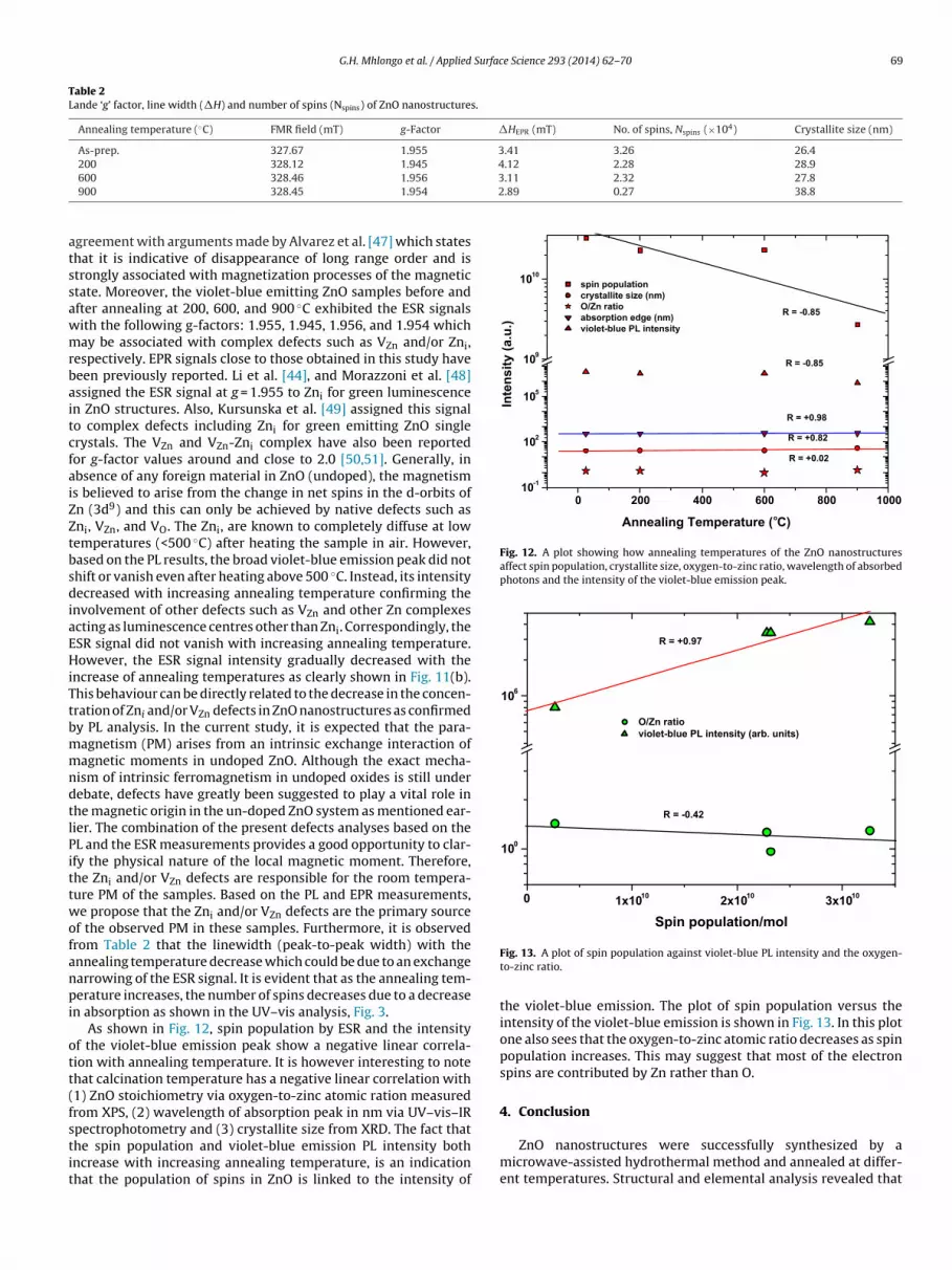
Fig. 12. A plot showing how annealing temperatures of the ZnO nanostructuresaffect spin population, crystallite size, oxygen-to-zinc ratio, wavelength of absorbedphotons and the intensity of the violet-blue emission peak.
0 1x10¹⁰ 2x10¹⁰ 3x10¹⁰
100
106
R = +0.97
R = -0.42
Spin population/mol
O/Zn ratio violet-blue PL intensity (arb. units)
600 328.46 1.956
900 328.45 1.954
greement with arguments made by Alvarez et al. [47] which stateshat it is indicative of disappearance of long range order and istrongly associated with magnetization processes of the magnetictate. Moreover, the violet-blue emitting ZnO samples before andfter annealing at 200, 600, and 900 ◦C exhibited the ESR signalsith the following g-factors: 1.955, 1.945, 1.956, and 1.954 whichay be associated with complex defects such as VZn and/or Zni,
espectively. EPR signals close to those obtained in this study haveeen previously reported. Li et al. [44], and Morazzoni et al. [48]ssigned the ESR signal at g = 1.955 to Zni for green luminescencen ZnO structures. Also, Kursunska et al. [49] assigned this signalo complex defects including Zni for green emitting ZnO singlerystals. The VZn and VZn-Zni complex have also been reportedor g-factor values around and close to 2.0 [50,51]. Generally, inbsence of any foreign material in ZnO (undoped), the magnetisms believed to arise from the change in net spins in the d-orbits ofn (3d9) and this can only be achieved by native defects such asni, VZn, and VO. The Zni, are known to completely diffuse at lowemperatures (<500 ◦C) after heating the sample in air. However,ased on the PL results, the broad violet-blue emission peak did nothift or vanish even after heating above 500 ◦C. Instead, its intensityecreased with increasing annealing temperature confirming the
nvolvement of other defects such as VZn and other Zn complexescting as luminescence centres other than Zni. Correspondingly, theSR signal did not vanish with increasing annealing temperature.owever, the ESR signal intensity gradually decreased with the
ncrease of annealing temperatures as clearly shown in Fig. 11(b).his behaviour can be directly related to the decrease in the concen-ration of Zni and/or VZn defects in ZnO nanostructures as confirmedy PL analysis. In the current study, it is expected that the para-agnetism (PM) arises from an intrinsic exchange interaction ofagnetic moments in undoped ZnO. Although the exact mecha-
ism of intrinsic ferromagnetism in undoped oxides is still underebate, defects have greatly been suggested to play a vital role inhe magnetic origin in the un-doped ZnO system as mentioned ear-ier. The combination of the present defects analyses based on theL and the ESR measurements provides a good opportunity to clar-fy the physical nature of the local magnetic moment. Therefore,he Zni and/or VZn defects are responsible for the room tempera-ure PM of the samples. Based on the PL and EPR measurements,e propose that the Zni and/or VZn defects are the primary source
f the observed PM in these samples. Furthermore, it is observedrom Table 2 that the linewidth (peak-to-peak width) with thennealing temperature decrease which could be due to an exchangearrowing of the ESR signal. It is evident that as the annealing tem-erature increases, the number of spins decreases due to a decrease
n absorption as shown in the UV–vis analysis, Fig. 3.As shown in Fig. 12, spin population by ESR and the intensity
f the violet-blue emission peak show a negative linear correla-ion with annealing temperature. It is however interesting to notehat calcination temperature has a negative linear correlation with1) ZnO stoichiometry via oxygen-to-zinc atomic ration measuredrom XPS, (2) wavelength of absorption peak in nm via UV–vis–IR
pectrophotometry and (3) crystallite size from XRD. The fact thathe spin population and violet-blue emission PL intensity bothncrease with increasing annealing temperature, is an indicationhat the population of spins in ZnO is linked to the intensity ofFig. 13. A plot of spin population against violet-blue PL intensity and the oxygen-to-zinc ratio.
the violet-blue emission. The plot of spin population versus theintensity of the violet-blue emission is shown in Fig. 13. In this plotone also sees that the oxygen-to-zinc atomic ratio decreases as spinpopulation increases. This may suggest that most of the electronspins are contributed by Zn rather than O.
4. Conclusion
ZnO nanostructures were successfully synthesized by amicrowave-assisted hydrothermal method and annealed at differ-ent temperatures. Structural and elemental analysis revealed that

7 Surfac
trtonZsccipdnb6ostct
A
eaa
R
[
[
[[
[[
[
[
[[
[
[
[
[
[
[[[[[
[[
[[
[[[[[
[[[
[
[[
[[[
[
0 G.H. Mhlongo et al. / Applied
he ZnO nanostructures are polycrystalline in nature with no impu-ity phases. Morphological variation upon increasing annealingemperature from well-defined “flower-like” structure composedf ZnO multi-nanorods to randomly oriented “worm-like” ZnOanostructures was also observed. The violet-blue emission fromnO nanostructured associated with VZn and Zni defects washown to decrease with increasing annealing temperature indi-ating reduction of the number of radiative recombination centresaused by decrease of concentration of VZn and/or Zni defects act-ng as luminescent centres in ZnO. The appearance of the phononeak at 580 cm−1 from Raman also confirmed the presence ofefects in ZnO nanostructures. The ESR analysis showed ESR sig-als with the g-factors of 1.955, 1.945, 1.956, and 1.954 which maye associated with VZn and/or Zni defects, for as prepared, 200,00, and 900 ◦C ZnO samples, respectively. The decrease in thexygen-to-zinc atomic ratio measured from XPS with increasingpin population suggests that most of the electron spins are con-ributed by Zn rather than O. Based on ESR and PL analyses, it wasoncluded that VZn and Zni defects are the main cause of the roomemperature PM of the ZnO nanostructures.
cknowledgement
This project is financially supported by the Department of Sci-nce and Technology of South Africa and the Council for Scientificnd Industrial Research of South Africa (Project numbers HGER28Pnd HGER27S).
eferences
[1] N.H. Alvi, K. ul Hasan, O. Nur, M. Willander, Nanoscale Res. Lett. 6 (2011) 130.[2] N.F. Hamedani, A.R. Mahjoub, A.A. Khodadadi, Y. Mortazavi, Sens. Actuators B
156 (2011) 737.[3] S.D. Shinde, G.E. Patil, D.D. Kajale, V.B. Gaikwad, G.H. Jain, J. Alloy Compd. 528
(2012) 109.[4] D.E. Motaung, G.H. Mhlongo, I. Kortidisd, S.S. Nkosi, G.F. Malgas, B.W.
Mwakikunga, S. Sinha Ray, G. Kiriakidis, Appl. Surf. Sci. 279 (2013) 142.[5] S.H. Ko, D. Lee, H.W. Kang, K.H. Nam, J.Y. Yeo, S.J. Hong, C.P. Grigoropoulos, H.J.
Sung, Nano Lett. 11 (2011) 666.[6] D.E. Motaung, G.F. Malgas, C.J. Arendse, S.E. Mavundla, Mater. Chem. Phys. 135
(2012) 401.[7] G. Zhang, X. Shen, Y. Yang, J. Phys. Chem. C 115 (2011) 7145.[8] P. Yang, H. Yan, S. Mao, R. Russo, J. Johnson, R. Saykally, N. Moris, J. Pham, R. He,
H.J. Choi, Adv. Funct. Mater. 12 (2002) 2.[9] M.H. Huang, S. Mao, H. Feick, H. Yan, Y. Wu, H. Kind, E. Weber, R. Russo, P. Yang,
Science 292 (2001) 1897.10] B. Xiang, P. Wang, X. Zhang, S.A. Dayeh, D.P.R. Aplin, C. Soci, D. Yu, D. Wang,
Nano Lett. 7 (2007) 2.11] Y. Wu, K.V. Rao, W. Voit, T. Tamaki, O.D. Jayakumar, L. Belova, Y.S. Liu, P.A. Glans,
C.L. Chang, J.H. Guo, IEEE Trans. Magn. 46 (2010) 6.12] M.D. McCluskey, S.J. Jokela, J. Appl. Phys. 106 (2009) 071101.13] L. Schmide-Mende, J.L. MacManus-Driscoll, Mater. Today 10 (2007) 40.
[
[
[
e Science 293 (2014) 62– 70
14] R.B. Kale, Y.J. Hsu, Y.F. Lin, S.Y. Lu, Solid State Commun. 42 (2007) 302.15] K.H. Tam, C.K. Cheung, Y.H. Leung, A.B. Djurisi, C.C. Ling, C.D. Beling, S. Fung,
W.M. Kwok, W.K. Chan, D.L. Phillips, L. Ding, W.K. Ge, J. Phys. Chem. B 110(2006) 20865.
16] G.H. Mhlongo, O.M. Ntwaeaborwa, H.C. Swart, R.E. Kroon, P. Solarz, W. Ryba-Romanowski, K.T. Hillie, J. Phys. Chem. C 115 (2011) 17625.
17] A. Djurisi, W.C.H. Chay, V.A.L. Roy, Y.H. Leung, C.Y. Kwong, K.W. Cheah, T.K.G.Rao, W.K. Chan, H.F. Lui, Adv. Funct. Mater. 14 (2004) 9.
18] L.H. Quanga, S.J. Chua, K.P. Loh, E. Fitzgerald, J. Cryst. Growth 287 (2006) 157.19] C. Jing-wei, X. Jian-ping, Z. Xiao-song, N.I.U. Xi-ping, X. Tong-yan, J.I. Ting, L.I.
Lan, Optoelectron. Lett. 8 (2012).20] Y. Yang, H. Yan, Z. Fu, B. Yang, L. Xia, Y. Xu, J. Zuo, F. Li, Solid State Commun. 138
(2006) 521.21] R.B.M. Cross, M.M. De Souza, E.M.S. Narayanan, Nanotechnology 16 (2005)
2188.22] L. Dai, X.L. Chen, W.J. Wang, T. Zhou, B.Q. Hu, J. Phys.: Condens. Matter 15 (2003)
2221.23] A.B. Djurisi, Y.H. Leung, K.H. Tam, Y.F. Hsu, L. Ding, W.K. Ge, Y.C. Zhong, K.S.
Wong, W.K. Chan, H.L. Tam, K.W. Cheah, W.M. Kwok, D.L. Phillips, Nanotech-nology 18 (2007) 095702.
24] Y. Zhang, Y. Liu, L. Wu, H. Li, L. Han, B. Wang, E. Xie, Appl. Surf. Sci. 255 (2009)4801.
25] H. Zeng, G. Duan, Y. Li, S. Yang, X. Xu, W. Cai, Adv. Funct. Mater. 20 (2010) 561.26] X. Zhang, Y. Xia, T. He, Mater. Chem. Phys. 137 (2012) 622.27] T.K. Kundu, N. Karak, P. Barik, S. Saha, Int. J. Soft Comput. Eng. 1 (2011) 2231.28] Y. Gupta, A. Mansingh, J. Appl. Phys. 80 (1996) 1063.29] N. Ashkenov, B.N. Mbenkum, C. Bundesmann, V. Riede, M. Lorenz, D. Spemann,
E.M. Kaidashev, A. Kasic, M. Schubert, M. Grundmann, J. Appl. Phys. 93 (2003)126.
30] C.J. Youn, T.S. Jeong, M.S. Han, J.H. Kim, J. Cryst. Growth 261 (2004) 526.31] K.A. Alim, V.A. Fonoberov, M. Shamsa, A.A. Balandin, J. Appl. Phys. 97 (2005)
124313.32] V.A. Fonoberov, A.A. Balandin, Phys. Rev. B 70 (2004) 195410.33] J. Yang, X. Liu, L. Yang, Y. Wang, Y. Zhang, J. Lang, M. Gao, B. Feng, J. Alloy Compd.
477 (2009) 632.34] Y. Zhao, Y. Jiang, Y. Fang, J. Cryst. Growth 307 (2007) 278.35] J.N. Zeng, J.K. Low, Z.M. Ren, T. Liew, Y.F. Lu, Appl. Surf. Sci. 197 (2002) 362.36] X.M. Fan, J.S. Lian, L. Zhao, Y.H. Liu, Appl. Surf. Sci. 252 (2005) 420.37] N.S. Ridhuan, K.A. Razak, Z. Lockman, A.A. Aziz, PLoS ONE 7 (2012) e50405.38] P.S. Xu, Y.M. Sun, C.S. Shi, F.Q. Xu, H.B. Pan, Nucl. Instr. Meth. Phys. Res. B 199
(2003) 286.39] B. Lin, Z. Fu, Y. Jia, Appl. Phys. Lett. 79 (2001) 943.40] E.G. Bylander, Appl. Phys. Lett. 49 (1978) 3.41] X.Q. Wei, B.Y. Man, M. Liu, C.S. Xue, H.Z. Zhuang, C. Yang, Physica B 388 (2007)
145.42] M. Chen, X. Wang, Y.H. Yu, Z.L. Pei, X.D. Bai, C. Sun, R.F. Huang, L.S. Wen, Appl.
Surf. Sci. 158 (2000) 134.43] P.T. Hsieh, Y.C. Chen, K.S. Kao, C.M. Wang, Appl. Phys. A 90 (2008) 317.44] L. Li, L. Fang, X. Ju Zhou, Z.Y. Liu, L. Zhao, S. Jiang, J. Electron Spectrosc. Relat.
Phenom. 173 (2009) 7.45] H. Wang, S. Dong, X. Zhou, X. Hu, Y. Chang, Physica E 44 (2011) 307.46] S. Wei, J. Lian, H. Wu, Mater. Characterization 61 (2010) 1239.47] G. Alvarez, H. Montiel, J.F. Barron, M.P. Gutierrez, R. Zamorano, J. Mag. Magn.
Mater. 322 (2010) 348.48] F. Morazzoni, R. Scotti, P. Di Nola, C. Milani, D. Narducci, J. Chem. Soc. Faraday
Trans. 88 (1992) 1691.
49] N.O. Korsunska, L.V. Borkovska, B.M. Bulakh, L.Y. Khomenkova, V.I. Kush-nirenko, I.V. Markevich, J. Lumin. 102–103 (2003) 733.50] M.G. Kakazey, M. Vlasova, M. Dominguez-Patin, G. Dominguez-Patin, G.
Gonzalez-Rodriguez, B. Salazar-Hernandez, J. Appl. Phys. 92 (2002) 5566.51] D. Galland, A. Herve, Solid State Comm. 14 (1974) 953.