tailoring graphene-based electrodes from semiconducting to
TRANSCRIPT
Tailoring graphene-based electrodes fromsemiconducting to metallic to increase theenergy density in supercapacitors
Jenel Vatamanu, Xiaojuan Ni, Feng Liu and Dmitry Bedrov
Department of Materials Science & Engineering, University of Utah, USA
E-mail: [email protected]
Received 6 July 2015, revised 6 September 2015Accepted for publication 30 September 2015Published 29 October 2015
AbstractThe semiconducting character of graphene and some carbon-based electrodes can lead tonoticeably lower total capacitances and stored energy densities in electric double layer (EDL)capacitors. This paper discusses the chemical and electronic structure modifications that enhancethe available energy bands, density of states and quantum capacitance of graphene substratesnear the Fermi level, therefore restoring the conducting character of these materials. The dopingof graphene with p or n dopants, such as boron and nitrogen atoms, or the introduction ofvacancy defects that introduce zigzag edges, can significantly increase the quantum capacitancewithin the potential range of interest for the energy storage applications by either shifting theDirac point away from the Fermi level or by eliminating the Dirac point. We show that acombination of doping and vacancies at realistic concentrations is sufficient to increase thecapacitance of a graphene-based electrode to within 1 μF cm−2 from that of a metallic surface.Using a combination of ab initio calculations and classical molecular dynamics simulations weestimate how the changes in the quantum capacitance of these electrode materials affect the totalcapacitance stored by the open structure EDL capacitors containing room temperature ionicliquid electrolytes.
Keywords: supercapacitors, quantum capacitance, modeling
(Some figures may appear in colour only in the online journal)
1. Introduction
In the context of increasing demand for electricity-basedenergy storage, experimental and theoretical research intovarious electrolytes at charged surfaces has increased sig-nificantly in the last decade. In particular, the electric doublelayer supercapacitors (EDLC) have been considered as pro-mising energy storage technologies [1–3]. In these devices theenergy storage is achieved due to non-Faradaic processes, i.e.,due to purely electrostatic interactions between the charged(porous) electrode and the electrolyte. This confers super-capacitors unique advantages such as fast charging rates, highdelivered power, and a virtually unlimited number of charge-discharge cycles. In EDLCs, the electrolyte typically consistsof a room temperature ionic liquid (RTIL) or organic solventwith high salt concentration. As for the electrode, carbon-
based materials are often preferred because they are relativelycheap, can be fabricated to have a highly porous structure(hence a high specific surface area) and are very versatile tofurther chemical functionalization. However, some carbon-based electrodes can show semiconducting properties leadingto lower electronic conductivity and lower capacitance. Forexample, electrodes based on single graphene sheets or somenanotubes can show semiconducting character [4]. Nanopor-ous electrodes such as, for example, carbide derived carbons(CDC), while being electronically conductive, can show astrong dependence of conductivity on the processing condi-tions and the resulting structural elements comprising theseelectrodes, indicating that the electronic properties in thesematerials are locally heterogeneous [5]. This can be a dis-advantage in energy storage applications because it dimin-ishes the stored energy densities.
Nanotechnology
Nanotechnology 26 (2015) 464001 (12pp) doi:10.1088/0957-4484/26/46/464001
0957-4484/15/464001+12$33.00 © 2015 IOP Publishing Ltd Printed in the UK1
If the quantum effects are accounted for, the total capa-citance of an electrode (C) can be modeled as two capacitorsconnected serially [6]: (i) a capacitor representing the quan-tum capacitance of the system (CQ) and (ii) a capacitorrepresenting the classical EDL capacitance (CEDL):
C C C
1 1 1. 1
Q EDL( )= +
The EDL capacitance (CEDL) originates from the pro-cesses of electrolyte rearrangement near the electrode surfaceas a response to the charge (or potential) applied on theelectrode surface. If the potential (or charge) is applied on theelectrode surface, the electrolyte will typically restructurenear the surface forming alternating layers of counter- and co-ions and hence leading to an oscillating space charge dis-tribution near the electrode. According to atomistic simula-tions [7] as well as atomic force microscopy [8, 9] and x-rayreflectometry [10, 11] experiments, such multilayer structurescan extend for up to 6 nm from the electrode surface. Notethat the interfacial layer can be overcharged, i.e., it can con-tain more counter-charge than the charge on the electrodesurface, and this excess counter-charge in the interfacial layeris compensated by the subsequent ion layers of the multilayerstructure. The resulting magnitude and the dependence of theelectrode capacitance on the electrode potential will bedetermined by such complex multilayer electrolyte orderingnear the surface. However, as it has been shown in our pre-vious simulations, the structural/charge correlations in theEDL within 2 nm from the electrode surface can quantita-tively explain all the features observed in the EDL differentialcapacitance (DC) as a function of electrode potential [12]. Formany commonly-used RTIL-based electrolytes the EDLcapacitance on metallic, atomically flat surfaces rangesbetween 4 and 6 μF cm−2, as shown by a series of simulations[7, 12–18] and experiments [19–23].
The quantum capacitance (CQ), on the other hand, ori-ginates from the quantum effects in the electrode material. Agrounded classical planar conductor completely screens outthe electrostatic field generated by a charge from penetrationto the other side of the plane. However, for a 2D electronicgas in a quantum well there can be a partial penetration of theelectrostatic field. Luryi [6] introduced the concept of thequantum capacitance in order to model with an equivalentcircuit (equation (1)) the partial penetrability of the electro-static field through a 2D electron gas in a quantum well. Theappearance of CQ is a consequence of the Pauli principle offilling out the energetic states with fermions and therefore it isquantified by the Fermi–Dirac distribution of the electronsover the available energy states. The CQ is important inelectronic nanodevices because it affects the transconductanceof the field-effect transistors [6, 24–26]. Also, the negativelocal quantum capacitance, that can occur if there is a positivecharge feedback (and is achievable, for example, in ferro-electrics [27] or in graphene nanoribbons [28]), can beemployed in the design of ‘smart gates’ for nanocircuits. Inthe context of energy storage devices, CQ is receivingincreasing attention because electrode materials with a high
CQ near Fermi level increase the stored energy density.However, as shown by experiments [29] and ab initionumerical calculations [30–32], the CQ for graphene has aU-shape dependence on the local gate potential varyingbetween ≈1 and 10 μF cm−2 in a typical potential range from−0.4 to +0.4 V. Note that the local potential gate is not theelectrode potential but instead it is a potential drop associatedwith the quantum capacitor serially connected with the EDLcapacitor. These values of CQ are comparable in magnitudewith the CEDL and hence can significantly influence the totalcapacitance of the electrode.
In this work we investigate the influence of the electrodestructure on the total capacitance of the open structure elec-trode/electrolyte systems using a combined ab initio DFT andclassical molecular dynamics (MD) simulation approach. Weshow that the semiconducting character of graphene (quanti-fied by the CQ) significantly changes the magnitude and theshape of the electrode DC, particularly near the potential ofzero charge (PZC). We discuss the structural modifications ofgraphene layers that can restore their conducting character.This could be achieved either by shifting the band structuresfrom the Fermi level (via e.g. doping) such that an increase inthe density of states (DOS) and the energy bands becomeavailable at and near the Fermi level, or by completelymodifying the symmetry of graphene (via generating vacancydefects) which eliminates the Dirac point and generates largeDOS at the Fermi level. We show that further increase of CQ,and hence the total capacitance, is possible if the electrodemodification depends on its polarity. For example, doping ofgraphene layers with n-type impurities (such as N atoms) onthe positive electrode and with the p-type impurities (such asB atoms) on the negative appears to optimize the CQ both onthe positive and negative plates, respectively.
2. Simulation methods
2.1 Ab initio calculations
The ab initio computations were performed utilizing theVASP package [33]. The electronic structure of pristine,doped or vacancy-defected graphene sheets were calculatedusing the projector augmented wave (PAW) method [34] forthe interaction between core and valence electrons and thePerdew–Burke–Ernzerhof (PBE) functional based on thegeneralized gradient approximation (GGA) [35] for theexchange-correlation interaction. The kinetic energy cut-offof 400 eV and 24×24×1 k-points were used. The com-putations were performed in two steps: in the first step, thestructure was relaxed to the minimum energy geometry, thenthe electronic properties, density of states (DOS) and the bandstructure (BS) were calculated for the equilibrated structure.The DOS were computed on a grid with energy steps of0.02 eV. For the graphene nanoribbons we computed thespin-polarized DOS for parallel and antiparallel configura-tions of spins at the opposite edges [36, 37]. The CQ wascalculated using obtained DOS, taking into account the 2Dsymmetry as derived in references [24, 30, 31]. As in [30], we
2
Nanotechnology 26 (2015) 464001 J Vatamanu et al
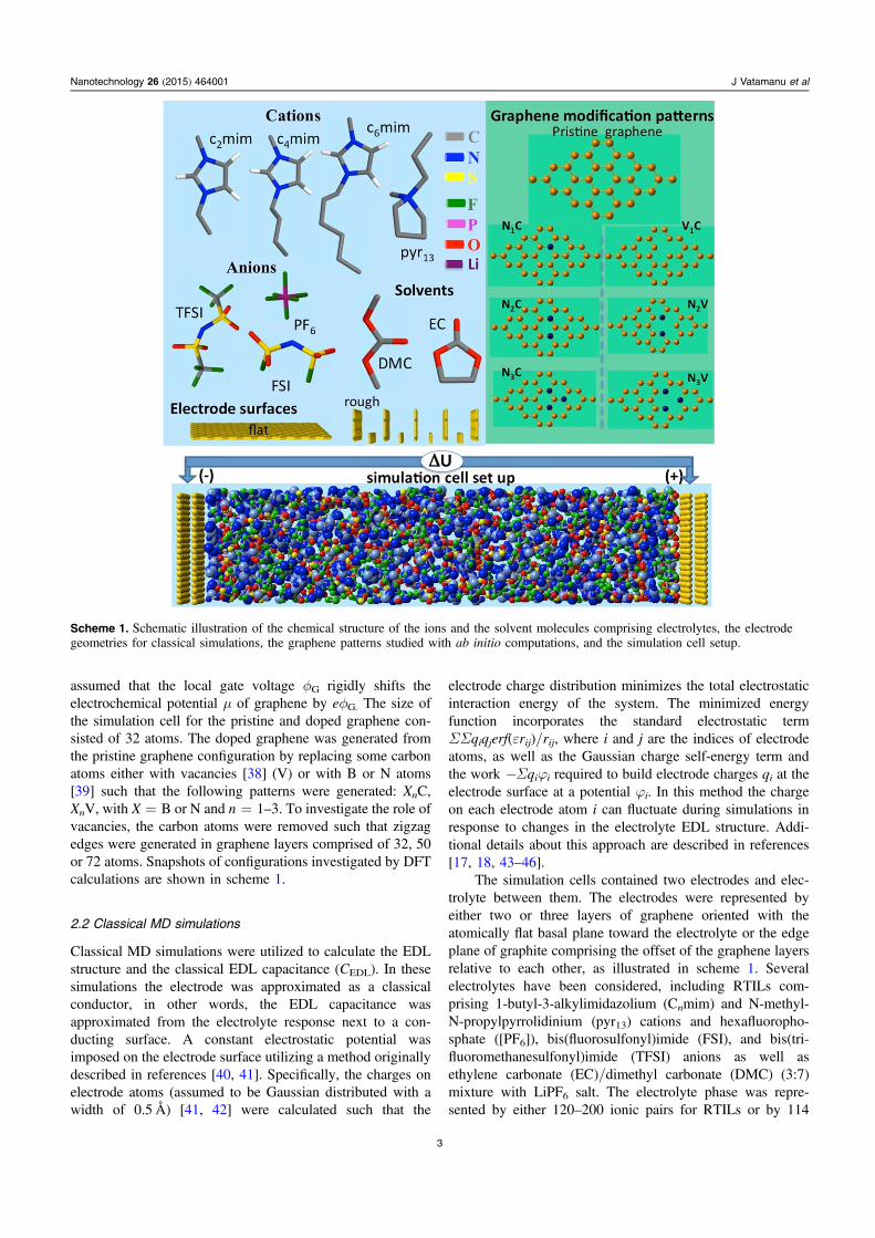
assumed that the local gate voltage fG rigidly shifts theelectrochemical potential μ of graphene by efG. The size ofthe simulation cell for the pristine and doped graphene con-sisted of 32 atoms. The doped graphene was generated fromthe pristine graphene configuration by replacing some carbonatoms either with vacancies [38] (V) or with B or N atoms[39] such that the following patterns were generated: XnC,XnV, with X=B or N and n=1–3. To investigate the role ofvacancies, the carbon atoms were removed such that zigzagedges were generated in graphene layers comprised of 32, 50or 72 atoms. Snapshots of configurations investigated by DFTcalculations are shown in scheme 1.
2.2 Classical MD simulations
Classical MD simulations were utilized to calculate the EDLstructure and the classical EDL capacitance (CEDL). In thesesimulations the electrode was approximated as a classicalconductor, in other words, the EDL capacitance wasapproximated from the electrolyte response next to a con-ducting surface. A constant electrostatic potential wasimposed on the electrode surface utilizing a method originallydescribed in references [40, 41]. Specifically, the charges onelectrode atoms (assumed to be Gaussian distributed with awidth of 0.5 Å) [41, 42] were calculated such that the
electrode charge distribution minimizes the total electrostaticinteraction energy of the system. The minimized energyfunction incorporates the standard electrostatic termΣΣqiqjerf(εrij)/rij, where i and j are the indices of electrodeatoms, as well as the Gaussian charge self-energy term andthe work −Σqiji required to build electrode charges qi at theelectrode surface at a potential ji. In this method the chargeon each electrode atom i can fluctuate during simulations inresponse to changes in the electrolyte EDL structure. Addi-tional details about this approach are described in references[17, 18, 43–46].
The simulation cells contained two electrodes and elec-trolyte between them. The electrodes were represented byeither two or three layers of graphene oriented with theatomically flat basal plane toward the electrolyte or the edgeplane of graphite comprising the offset of the graphene layersrelative to each other, as illustrated in scheme 1. Severalelectrolytes have been considered, including RTILs com-prising 1-butyl-3-alkylimidazolium (Cnmim) and N-methyl-N-propylpyrrolidinium (pyr13) cations and hexafluoropho-sphate ([PF6]), bis(fluorosulfonyl)imide (FSI), and bis(tri-fluoromethanesulfonyl)imide (TFSI) anions as well asethylene carbonate (EC)/dimethyl carbonate (DMC) (3:7)mixture with LiPF6 salt. The electrolyte phase was repre-sented by either 120–200 ionic pairs for RTILs or by 114
Scheme 1. Schematic illustration of the chemical structure of the ions and the solvent molecules comprising electrolytes, the electrodegeometries for classical simulations, the graphene patterns studied with ab initio computations, and the simulation cell setup.
3
Nanotechnology 26 (2015) 464001 J Vatamanu et al
molecules of EC, 256 molecules of DMC and 31 LiPF6 pairs.These amounts of electrolyte were sufficient to create aseparation between electrodes of about 11–20 nm, thereforeallowing a sufficient amount of bulk electrolyte to separatethe EDLs formed at the electrodes. The RTILs were modeledusing the force fields described in [12] for [C4mim][PF6], in[7] for [Cnmim][FSI], in [14] for [Cnmim][TFSI], in [47] for[pyr13][FSI] RTILs and in [48] for EC/DMC/LiPF6 elec-trolyte. Note that RTIL electrolytes were modeled using anonpolarizable mixed atomistic and united atom model whilesimulations of the EC/DMC/LiPF6 system employed a fullyatomistic, polarizable APPLE&P force field [48]. The polar-izability of this electrolyte was represented classically withinduced dipoles computed via self-consistent iterations. Anillustration of the typical simulation setup and the moleculescomprising electrolytes are also shown in scheme 1.
The long-range electrostatic interactions were calculatedwith the Ewald summation method adapted for the 2D geo-metry [49, 50]. The reciprocal part of the Ewald summationwas handled with an efficient SPME method for the 2Dsymmetry proposed by Kawata and co-workers [51–54]. Theshort-range interactions (the van der Waals and the real partof the SPME) were calculated within a spherical cut-off of10 Å. A reversible multiple-time step algorithm [55] wasutilized to integrate the equations of motions as follows. Theforces from bonds, bends, and out-of-plane deformationswere computed every τ/10, the forces from dihedrals andforces due to nonbonded interactions (van der Waals and thereal part of electrostatic interactions) within a cutoff radius of7.5 Å were updated every τ/2, and the remaining nonbondedforces (i.e., the van der Waals and electrostatic interactionswithin the 10.0 Å cut off and the reciprocal part of SPME)were computed every τ, where the timescale τ was 3 fs for theEC/DMC/LiPF6 system and 5 fs for the systems with RTILelectrolytes. The electrode charges were updated every 50τ.Each system was simulated at 10–20 different appliedpotential differences between the electrodes in the rangebetween 0 and 6 V. A typical length of the simulation tra-jectory was between 10 and 40 ns depending on the mobilityof bulk electrolyte near electrode surface. The temperature ofthe simulations of systems with RTIL electrolytes was 393 Kwhile the EC/DMC/LiPF6 system was simulated at 453 K.The temperature was controlled with Nosé–Hoover chainthermostats [56].
Using the charge distribution across the asymmetrydirection averaged over simulation trajectories, the corre-sponding screened Poisson potential was calculated using anumerical integration of the 1D-Poisson equation. The dif-ference in the Poisson potential between bulk electrolyte andelectrode surface defined the EDL potential (UEDL). TheUEDL corresponding to uncharged electrodes defined thepotential of zero charge (PZC). The electrode potential of aconducting electrode (Ve) is then the difference between theUEDL and the PZC, Ve=UEDL-PZC.
2.3 Combined analysis
As mentioned above, the total electrode capacitance (C) canbe calculated using equation (1). The total potential drop (Va)between the electrode and the bulk electrolyte (that can berepresented as serially connected classical and quantumcapacitors) is then the sum of the local gate potential (Vg) onthe capacitor representing the quantum effects and thepotential drop on the ‘classical’ (EDL) capacitor,Va=Vg+Ve=Vg+UEDL-PZC. The PZC and the UEDL
were taken from MD simulations near conducting surfaceswhile the local (quantum) gate potential was approximated asVg=−(E-EFermi)/e from the DFT calculations [31]. The Vg
was computed based on the total electrode charge, i.e., bothquantum and classical capacitors were assumed to have thesame charge because they are serially connected, as describedin [31]. Other approximations utilized here were similar tothose in previous Paek et al works [30, 31, 57–60]. Due tolimited electrolyte electrochemical stability, the total electrodepotential in the EDL supercapacitors typically varies withinthe range −3 to +3 V. Note that the CQ increases sharply withpotential. Therefore a typical range of the local gate voltageVg of interest for the energy storage applications is within|Vg|<0.5 V. The following differential capacitances will bediscussed in the paper: the EDL capacitance CEDL obtainedfrom MD simulations on a metallic surface, the quantumcapacitance of the electrode CQ extracted from DFT predictedDOS, and the total capacitance of a semiconducting electrodeC defined by equation (1). It is important to recall that ourapproach neglects the role of electrolyte proximity on theband structure of the electrode. In other words, the bands wereassumed to be affected only by the structural impurities ingraphene. Also we approximate the capacitance associatedwith electrolyte reordering near a semiconducting electrode tobe the same as for a metallic electrode. Similar approxima-tions were previously utilized by Paek and co-work-ers [30, 31].
3. Results and discussion
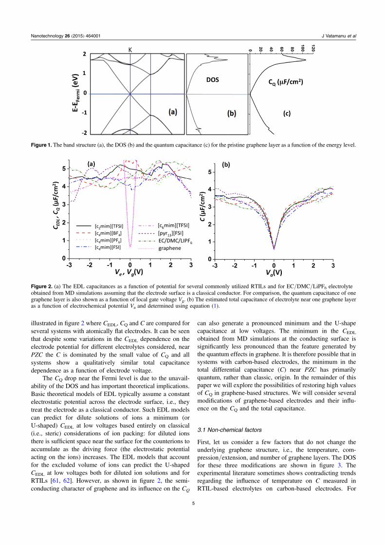
Figure 1 shows the band structure, DOS and CQ for a singlepristine graphene layer. Because of the presence of the Diracpoint in the band structure at the K-point (figure 1(a)), theDOS has a U-shape dependence on the energy and a mini-mum at the Fermi level. As a result of such DOS dependence,the CQ also has a minimum at the Fermi level and therefore aU-shaped dependence on the local gate voltage. Although at |Vg|>1 V, the CQ becomes higher than 25 μF cm−2 at lowerVg, which are more relevant for the energy storage applica-tions, and the CQ is smaller or comparable to the CEDL fortypical electrolytes. Previous simulations [15] and experi-ments [19, 21] probed whether CEDL near flat conductingelectrodes for typical RTILs varies between 4.0–5.5 μF cm−2.However, the CQ of a single graphene sheet has a dramaticdrop near PZC. Therefore the semiconducting character ofgraphene can generate a significant drop in the total electrodecapacitance, especially at low electrode potentials, as
4
Nanotechnology 26 (2015) 464001 J Vatamanu et al
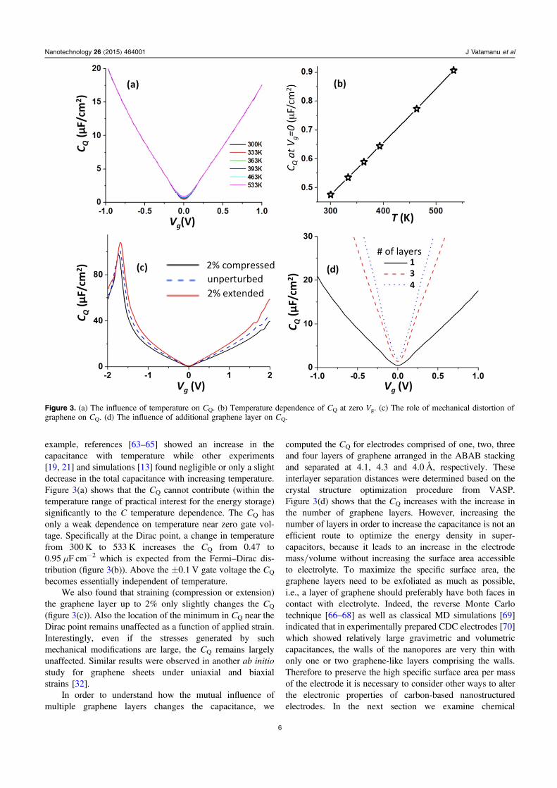
illustrated in figure 2 where CEDL, CQ and C are compared forseveral systems with atomically flat electrodes. It can be seenthat despite some variations in the CEDL dependence on theelectrode potential for different electrolytes considered, nearPZC the C is dominated by the small value of CQ and allsystems show a qualitatively similar total capacitancedependence as a function of electrode voltage.
The CQ drop near the Fermi level is due to the unavail-ability of the DOS and has important theoretical implications.Basic theoretical models of EDL typically assume a constantelectrostatic potential across the electrode surface, i.e., theytreat the electrode as a classical conductor. Such EDL modelscan predict for dilute solutions of ions a minimum (orU-shaped) CEDL at low voltages based entirely on classical(i.e., steric) considerations of ion packing: for diluted ionsthere is sufficient space near the surface for the counterions toaccumulate as the driving force (the electrostatic potentialacting on the ions) increases. The EDL models that accountfor the excluded volume of ions can predict the U-shapedCEDL at low voltages both for diluted ion solutions and forRTILs [61, 62]. However, as shown in figure 2, the semi-conducting character of graphene and its influence on the CQ
can also generate a pronounced minimum and the U-shapecapacitance at low voltages. The minimum in the CEDL
obtained from MD simulations at the conducting surface issignificantly less pronounced than the feature generated bythe quantum effects in graphene. It is therefore possible that insystems with carbon-based electrodes, the minimum in thetotal differential capacitance (C) near PZC has primarilyquantum, rather than classic, origin. In the remainder of thispaper we will explore the possibilities of restoring high valuesof CQ in graphene-based structures. We will consider severalmodifications of graphene-based electrodes and their influ-ence on the CQ and the total capacitance.
3.1 Non-chemical factors
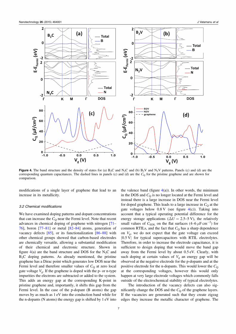
First, let us consider a few factors that do not change theunderlying graphene structure, i.e., the temperature, com-pression/extension, and number of graphene layers. The DOSfor these three modifications are shown in figure 3. Theexperimental literature sometimes shows contradicting trendsregarding the influence of temperature on C measured inRTIL-based electrolytes on carbon-based electrodes. For
Figure 1. The band structure (a), the DOS (b) and the quantum capacitance (c) for the pristine graphene layer as a function of the energy level.
Figure 2. (a) The EDL capacitances as a function of potential for several commonly utilized RTILs and for EC/DMC/LiPF6 electrolyteobtained from MD simulations assuming that the electrode surface is a classical conductor. For comparison, the quantum capacitance of onegraphene layer is also shown as a function of local gate voltage Vg. (b) The estimated total capacitance of electrolyte near one graphene layeras a function of electrochemical potential Va and determined using equation (1).
5
Nanotechnology 26 (2015) 464001 J Vatamanu et al
example, references [63–65] showed an increase in thecapacitance with temperature while other experiments[19, 21] and simulations [13] found negligible or only a slightdecrease in the total capacitance with increasing temperature.Figure 3(a) shows that the CQ cannot contribute (within thetemperature range of practical interest for the energy storage)significantly to the C temperature dependence. The CQ hasonly a weak dependence on temperature near zero gate vol-tage. Specifically at the Dirac point, a change in temperaturefrom 300 K to 533 K increases the CQ from 0.47 to0.95 μF cm−2 which is expected from the Fermi–Dirac dis-tribution (figure 3(b)). Above the ±0.1 V gate voltage the CQ
becomes essentially independent of temperature.We also found that straining (compression or extension)
the graphene layer up to 2% only slightly changes the CQ
(figure 3(c)). Also the location of the minimum in CQ near theDirac point remains unaffected as a function of applied strain.Interestingly, even if the stresses generated by suchmechanical modifications are large, the CQ remains largelyunaffected. Similar results were observed in another ab initiostudy for graphene sheets under uniaxial and biaxialstrains [32].
In order to understand how the mutual influence ofmultiple graphene layers changes the capacitance, we
computed the CQ for electrodes comprised of one, two, threeand four layers of graphene arranged in the ABAB stackingand separated at 4.1, 4.3 and 4.0 Å, respectively. Theseinterlayer separation distances were determined based on thecrystal structure optimization procedure from VASP.Figure 3(d) shows that the CQ increases with the increase inthe number of graphene layers. However, increasing thenumber of layers in order to increase the capacitance is not anefficient route to optimize the energy density in super-capacitors, because it leads to an increase in the electrodemass/volume without increasing the surface area accessibleto electrolyte. To maximize the specific surface area, thegraphene layers need to be exfoliated as much as possible,i.e., a layer of graphene should preferably have both faces incontact with electrolyte. Indeed, the reverse Monte Carlotechnique [66–68] as well as classical MD simulations [69]indicated that in experimentally prepared CDC electrodes [70]which showed relatively large gravimetric and volumetriccapacitances, the walls of the nanopores are very thin withonly one or two graphene-like layers comprising the walls.Therefore to preserve the high specific surface area per massof the electrode it is necessary to consider other ways to alterthe electronic properties of carbon-based nanostructuredelectrodes. In the next section we examine chemical
Figure 3. (a) The influence of temperature on CQ. (b) Temperature dependence of CQ at zero Vg. (c) The role of mechanical distortion ofgraphene on CQ. (d) The influence of additional graphene layer on CQ.
6
Nanotechnology 26 (2015) 464001 J Vatamanu et al
modifications of a single layer of graphene that lead to anincrease in its metallicity.
3.2 Chemical modifications
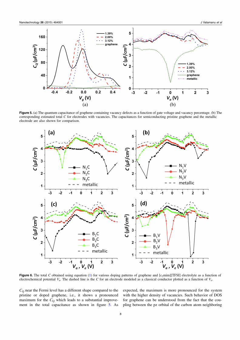
We have examined doping patterns and dopant concentrationsthat can increase the CQ near the Fermi level. Note that recentadvances in chemical doping of graphene with nitrogen [71–76], boron [77–81] or metal [82–84] atoms, generation ofvacancy defects [85], or its functionalization [86–88] withother chemical groups showed that carbon-based electrodesare chemically versatile, allowing a substantial modificationof their chemical and electronic structure. Shown infigure 4(a) are the band structure and DOS for the N2C andB2C doping patterns. As already mentioned, the pristinegraphene has a Dirac point which generates low DOS near theFermi level and therefore smaller values of CQ at zero localgate voltage Vg. If the graphene is doped with the p- or n-typeimpurities the electrons are subtracted or added to the system.This adds an energy gap at the corresponding K-point inpristine graphene and, importantly, it shifts this gap from theFermi level. In the case of the p-dopant (B atoms) the gapmoves by as much as 1 eV into the conduction band while forthe n-dopants (N atoms) the energy gap is shifted by 1 eV into
the valence band (figure 4(a)). In other words, the minimumin the DOS and CQ is no longer located at the Fermi level andinstead there is a large increase in DOS near the Fermi levelfor doped graphene. This leads to a large increase in CQ at thegate voltages below 0.8 V (see figure 4(c)). Taking intoaccount that a typical operating potential difference for theenergy storage applications (ΔU=2.5–5 V), the relativelysmall values of CEDL on the flat surfaces (4–6 μF cm−2) forcommon RTILs, and the fact that CQ has a sharp dependenceon Vg, we do not expect that the gate voltage can exceed|0.5 V| for typical supercapacitors with RTIL electrolytes.Therefore, in order to increase the electrode capacitance, it issufficient to design doping that would move the band gapaway from the Fermi level by about 0.5 eV. Clearly, withsuch doping at certain values of Vg an energy gap will beobserved at the negative electrode for the p-dopants and at thepositive electrode for the n-dopants. This would lower the CQ
at the corresponding voltages, however this would onlyhappen at very large electrode voltages which commonly fallsoutside of the electrochemical stability of typical electrolytes.
The introduction of the vacancy defects can also sig-nificantly change the DOS and the CQ of the graphene layers.If the vacancies are generated such that they create zigzagedges they increase the metallic character of graphene. The
Figure 4. The band structure and the density of states for (a) B2C and N2C and (b) B2V and N2V patterns. Panels (c) and (d) are thecorresponding quantum capacitances. The dashed lines in panels (c) and (d) are the CQ for the pristine graphene and are shown forcomparison.
7
Nanotechnology 26 (2015) 464001 J Vatamanu et al
CQ near the Fermi level has a different shape compared to thepristine or doped graphene, i.e., it shows a pronouncedmaximum for the CQ which leads to a substantial improve-ment in the total capacitance as shown in figure 5. As
expected, the maximum is more pronounced for the systemwith the higher density of vacancies. Such behavior of DOSfor graphene can be understood from the fact that the cou-pling between the pz orbital of the carbon atom neighboring
Figure 5. (a) The quantum capacitance of graphene containing vacancy defects as a function of gate voltage and vacancy percentage. (b) Thecorresponding estimated total C for electrodes with vacancies. The capacitances for semiconducting pristine graphene and the metallicelectrode are also shown for comparison.
Figure 6. The total C obtained using equation (1) for various doping patterns of graphene and [c2mim][TFSI] electrolyte as a function ofelectrochemical potential Va. The dashed line is the C for an electrode modeled as a classical conductor plotted as a function of Ve.
8
Nanotechnology 26 (2015) 464001 J Vatamanu et al
the vacancy and the sp2 orbitals introduces nonequivalentspin states that destroy the Dirac point [89, 90].
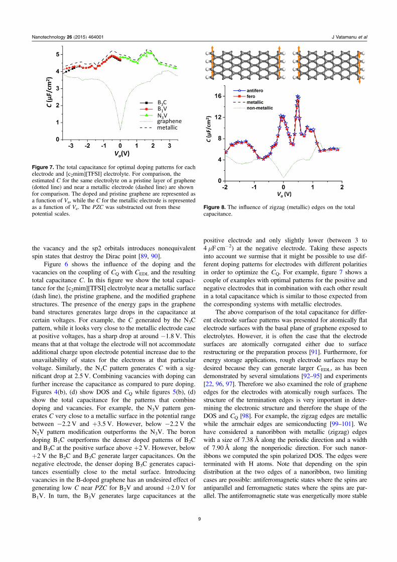
Figure 6 shows the influence of the doping and thevacancies on the coupling of CQ with CEDL and the resultingtotal capacitance C. In this figure we show the total capaci-tance for the [c2mim][TFSI] electrolyte near a metallic surface(dash line), the pristine graphene, and the modified graphenestructures. The presence of the energy gaps in the grapheneband structures generates large drops in the capacitance atcertain voltages. For example, the C generated by the N3Cpattern, while it looks very close to the metallic electrode caseat positive voltages, has a sharp drop at around −1.8 V. Thismeans that at that voltage the electrode will not accommodateadditional charge upon electrode potential increase due to theunavailability of states for the electrons at that particularvoltage. Similarly, the N1C pattern generates C with a sig-nificant drop at 2.5 V. Combining vacancies with doping canfurther increase the capacitance as compared to pure doping.Figures 4(b), (d) show DOS and CQ while figures 5(b), (d)show the total capacitance for the patterns that combinedoping and vacancies. For example, the N3V pattern gen-erates C very close to a metallic surface in the potential rangebetween −2.2 V and +3.5 V. However, below −2.2 V theN2V pattern modification outperforms the N3V. The borondoping B1C outperforms the denser doped patterns of B2Cand B3C at the positive surface above +2 V. However, below+2 V the B2C and B3C generate larger capacitances. On thenegative electrode, the denser doping B3C generates capaci-tances essentially close to the metal surface. Introducingvacancies in the B-doped graphene has an undesired effect ofgenerating low C near PZC for B2V and around +2.0 V forB1V. In turn, the B3V generates large capacitances at the
positive electrode and only slightly lower (between 3 to4 μF cm−2) at the negative electrode. Taking these aspectsinto account we surmise that it might be possible to use dif-ferent doping patterns for electrodes with different polaritiesin order to optimize the CQ. For example, figure 7 shows acouple of examples with optimal patterns for the positive andnegative electrodes that in combination with each other resultin a total capacitance which is similar to those expected fromthe corresponding systems with metallic electrodes.
The above comparison of the total capacitance for differ-ent electrode surface patterns was presented for atomically flatelectrode surfaces with the basal plane of graphene exposed toelectrolytes. However, it is often the case that the electrodesurfaces are atomically corrugated either due to surfacerestructuring or the preparation process [91]. Furthermore, forenergy storage applications, rough electrode surfaces may bedesired because they can generate larger CEDL, as has beendemonstrated by several simulations [92–95] and experiments[22, 96, 97]. Therefore we also examined the role of grapheneedges for the electrodes with atomically rough surfaces. Thestructure of the termination edges is very important in deter-mining the electronic structure and therefore the shape of theDOS and CQ [98]. For example, the zigzag edges are metallicwhile the armchair edges are semiconducting [99–101]. Wehave considered a nanoribbon with metallic (zigzag) edgeswith a size of 7.38 Å along the periodic direction and a widthof 7.90 Å along the nonperiodic direction. For such nanor-ibbons we computed the spin polarized DOS. The edges wereterminated with H atoms. Note that depending on the spindistribution at the two edges of a nanoribbon, two limitingcases are possible: antiferromagnetic states where the spins areantiparallel and ferromagnetic states where the spins are par-allel. The antiferromagnetic state was energetically more stable
Figure 7. The total capacitance for optimal doping patterns for eachelectrode and [c2mim][TFSI] electrolyte. For comparison, theestimated C for the same electrolyte on a pristine layer of graphene(dotted line) and near a metallic electrode (dashed line) are shownfor comparison. The doped and pristine graphene are represented asa function of Va, while the C for the metallic electrode is representedas a function of Ve. The PZC was substracted out from thesepotential scales.
Figure 8. The influence of zigzag (metallic) edges on the totalcapacitance.
9
Nanotechnology 26 (2015) 464001 J Vatamanu et al
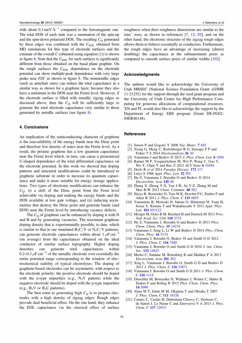
with about 0.3 meVÅ−1 compared to the ferromagnetic one.The total DOS of each state was a summation of the spin-upand the spin-down polarized DOS. The resulting CQ generatedby these edges was combined with the CEDL obtained fromMD simulations for this type of electrode surfaces and theestimate of the overall C (obtained using equation (1)) is shownin figure 8. Note that the CEDL for such surfaces is significantlydifferent from those obtained on the basal plane graphite. Onthe rough surfaces the CEDL dependence on the electrodepotential can show multiple-peak dependence with very largepeaks near PZC as shown in figure 8. The nonmetallic edges(such as armchair ones) can reduce the total capacitance in asimilar way as shown for a graphene layer, because they alsohave a minimum in the DOS near the Fermi level. However, ifthe electrode surface is filled with metallic zigzag edges asdiscussed above, then the CQ will be sufficiently large togenerate the total electrode capacitance very similar to thosegenerated by metallic surfaces (see figure 8).
4. Conclusions
An implication of the semiconducting character of grapheneis the unavailability of the energy bands near the Dirac pointand therefore low density of states near the Fermi level. As aresult, the pristine graphene has a low quantum capacitancenear the Fermi level which, in turn, can cause a pronouncedU-shaped dependence of the total differential capacitance onthe electrode potential. In this work we showed that dopingpatterns and structural modifications could be introduced tographene substrate in order to increase its quantum capaci-tance and make it more suitable for energy storage applica-tions. Two types of electronic modifications can enhance theCQ: (i) a shift of the Dirac point from the Femi levelachievable via doping and making the energy bands and theDOS available at low gate voltage, and (ii) inducing asym-metries that destroy the Dirac point and generate bands (andDOS) near the Fermi level by introducing vacancy defects.
The CQ of graphene can be enhanced by doping it with Nand B and by generating vacancies. The maximum graphenedoping density that is experimentally possible, to date, whichis similar to that in our simulated B1C/V or N1C/V patterns,can generate electrode capacitances within about 1 μF cm−2
(on average) from the capacitances obtained on the idealconductor of similar surface topography. Higher dopingdensities can generate total capacitances within0.2–0.3 μF cm−2 of the metallic electrode over essentially theentire potential range corresponding to the window of elec-trochemical stability of typical electrolytes. The doping ofgraphene-based electrodes can be asymmetric with respect tothe electrode polarity: the positive electrode should be dopedwith the n-type impurities (e.g., N3V pattern) while thenegative electrode should be doped with the p-type impurities(e.g., B1V or B3C patterns).
The best route to generating high CQ is to prepare elec-trodes with a high density of zigzag edges. Rough edgesprovide dual beneficial effect. On the one hand, they enhancethe EDL capacitance via the classical effect of surface
roughness when their roughness dimensions are similar to theions’ sizes, as shown in references [7, 12, 93], and on theother hand, the electronic structure of the zigzag rough edgesallows them to behave essentially as conductors. Furthermore,the rough edges have an advantage of increasing (almostdoubling) the capacitance in the subnanometer pores ascompared to smooth surface pores of similar widths [102].
Acknowledgments
The authors would like to acknowledge the University ofUtah MRSEC (National Science Foundation Grant #DMR11-21252) for the support through the seed grant program andthe University of Utah Center for High Performance Com-puting for generous allocations of computational resources.XN and FL would also like to acknowledge the support by theDepartment of Energy EBS program (Grant DE-FG02-04ER46148).
References
[1] Simon P and Gogotsi Y 2008 Nat. Mater. 7 845[2] Xiong G, Meng C, Reifenberger R G, Irazoqui P P and
Fisher T S 2014 Electroanalysis 26 30[3] Vatamanu J and Bedrov D 2015 J. Phys. Chem. Lett. 6 3594[4] Ramuz M P, Vosgueritchian M, Wei P, Wang C, Gao Y,
Wu Y, Chen Y and Bao Z 2012 ACS Nano 6 10384[5] Dryfe R et al 2014 Faraday Discuss. 172 117[6] Luryi S 1988 Appl. Phys. Lett. 52 501[7] Hu Z, Vatamanu J, Borodin O and Bedrov D 2014
Electrochim. Acta 145 40[8] Zhang X, Zhong Y-X, Yan J-W, Su Y-Z, Zhang M and
Mao B-W 2012 Chem. Commun. 48 582[9] Hayes R, Borisenko N, Tam M K, Howlett P C, Endres F and
Atkin R 2011 J. Phys. Chem. C 115 6855[10] Yamamoto R, Morisaki H, Sakata O, Shimotani H, Yuan H,
Iwasa Y, Kimura T and Wakabayashi Y 2012 Appl. Phys.Lett. 101 053122
[11] Mezger M, Ocko B M, Reichert H and Deutsch M 2013 Proc.Natl Acad. Sci. USA 110 3733
[12] Hu Z, Vatamanu J, Borodin O and Bedrov D 2013 Phys.Chem. Chem. Phys. 15 14234
[13] Vatamanu J, Xing L, Li W and Bedrov D 2014 Phys. Chem.Chem. Phys. 16 5174
[14] Vatamanu J, Borodin O, Bedrov D and Smith G D 2012J. Phys. Chem. C 116 7940
[15] Vatamanu J, Borodin O and Smith G D 2010 J. Am. Chem.Soc. 132 14825
[16] Merlet C, Salanne M, Rotenberg B and Madden P A 2013Electrochim. Acta 101 262
[17] Xing L, Vatamanu J, Borodin O, Smith G D and Bedrov D2012 J. Phys. Chem. C 116 23871
[18] Vatamanu J, Borodin O and Smith G D 2011 J. Phys. Chem.C 116 1114
[19] Druschler M, Borisenko N, Wallauer J, Winter C, Huber B,Endres F and Roling B 2012 Phys. Chem. Chem. Phys.14 5090
[20] Alam M T, Islam M M, Okajima T and Ohsaka T 2007J. Phys. Chem. C 111 18326
[21] Cannes C, Cachet H, Debiemme-Chouvy C, Deslouis C,de Sanoit J, Le Naour C and Zinovyeva V A 2013 J. Phys.Chem. C 117 22915
10
Nanotechnology 26 (2015) 464001 J Vatamanu et al
[22] Costa R, Pereira C M and Silva A F 2015 Electrochim. Acta167 421
[23] Gomes C, Costa R, Pereira C M and Silva A F 2014 RSC Adv.4 28914
[24] John D L, Castro L C and Pulfrey D L 2004 J. Appl. Phys.96 5180
[25] Yan Q, Huang B, Yu J, Zheng F, Zang J, Wu J, Gu B-L,Liu F and Duan W 2007 Nano Lett. 7 1469
[26] Huang B, Yan Q, Zhou G, Wu J, Gu B-L, Duan W and Liu F2007 Appl. Phys. Lett. 91 253122
[27] Salvatore G A, Lattanzio L, Bouvet D, Stolichnov I,Setter N and Ionescu A M 2010 Appl. Phys. Lett. 97 053503
[28] Reiter R, Derra U, Birner S, Terrés B, Libisch F,Burgdörfer J and Stampfer C 2014 Phys. Rev. B 89 115406
[29] Xia J, Chen F, Li J and Tao N 2009 Nat. Nanotechnology4 505
[30] Paek E, Pak A J, Kweon K E and Hwang G S 2013 J. Phys.Chem. C 117 5610
[31] Paek E, Pak A J and Hwang G S 2013 J. Electrochem. Soc.160 A1
[32] Wood B C, Ogitsu T, Otani M and Biener J 2014 J. Phys.Chem. C 118 4
[33] Hafner J 2008 J. Comput. Chem. 29 2044[34] Blöchl P E 1994 Phys. Rev. B 50 17953[35] Perdew J P, Burke K and Ernzerhof M 1996 Phys. Rev. Lett.
77 3865[36] Yu D, Lupton E, Gao H J, Zhang C and Liu F 2008 Nano Res.
1 497[37] Yu D, Lupton E, Liu M, Liu W and Liu F 2008 Nano Res.
1 56[38] Liu W, Wang Z F, Shi Q W, Yang J and Liu F 2009 Phys.
Rev. B 80 233405[39] Chen L, Hu H, Ouyang Y, Pan H Z, Sun Y Y and Liu F 2011
Carbon 49 3356[40] Siepmann J I and Sprik M 1995 J. Chem. Phys. 102 511[41] Reed S K, Lanning O J and Madden P A 2007 J. Chem. Phys.
126 084704[42] Vatamanu J, Borodin O and Smith G D 2010 Phys. Chem.
Chem. Phys. 12 170[43] Pastewka L, Järvi T T, Mayrhofer L and Moseler M 2011
Phys. Rev. B 83 165418[44] Wang Z, Yang Y, Olmsted D L, Asta M and Laird B B 2014
J. Chem. Phys. 141 184102[45] Kiss P T, Sega M and Baranyai A 2014 J. Chem. Theory
Comput. 10 5513[46] Golze D, Iannuzzi M, Nguyen M-T, Passerone D and Hutter J
2013 J. Chem. Theory Comput. 9 5086[47] Vatamanu J, Borodin O and Smith G D 2011 J. Phys. Chem.
B 115 3073[48] Borodin O 2009 J. Phys. Chem. B 113 11463[49] Heyes D M 1994 Phys. Rev. B 49 755[50] Heyes D M 1984 Phys. Rev. B 30 2182[51] Kawata M and Mikami M 2001 Chem. Phys. Lett. 340 157[52] Kawata M, Mikami M and Nagashima U 2002 J. Chem. Phys.
116 3430[53] Kawata M, Mikami M and Nagashima U 2001 J. Chem. Phys.
115 4457[54] Kawata M and Nagashima U 2001 Chem. Phys. Lett. 340 165[55] Martyna G J, Tuckerman M E, Tobias D J and Klein M L
1996 Mol. Phys. 87 1117[56] Hoover W G 1985 Phys. Rev. A 31 1695[57] Paek E, Pak A J and Hwang G S 2015 J. Chem. Phys. 142
024701[58] Paek E, Pak A J and Hwang G S 2013 J. Phys. Chem. C 117
23539[59] Pak A J, Paek E and Hwang G S 2013 Phys. Chem. Chem.
Phys. 15 19741[60] Pak A J, Paek E and Hwang G S 2014 Carbon 68 734[61] Kornyshev A A 2007 J. Phys. Chem. B 111 5545
[62] Oldham K B 2008 J. Electroanal. Chem. 613 131[63] Silva F, Gomes C, Figueiredo M, Costa R, Martins A and
Pereira C M 2008 J. Electroanal. Chem. 622 153[64] Costa R, Pereira C M and Silva F 2010 Phys. Chem. Chem.
Phys. 12 11125[65] Alam M T, Masud J, Islam M M, Okajima T and Ohsaka T
2011 J. Phys. Chem. C 115 19797[66] Pikunic J, Clinard C, Cohaut N, Gubbins K E, Guet J-M,
Pellenq R J M, Rannou I and Rouzaud J-N 2003 Langmuir19 8565
[67] Zetterström P, Urbonaite S, Lindberg F, Delaplane R G,Leis J and Svensson G 2005 J. Phys.: Condens. Matter17 3509
[68] Jain S K, Pellenq R J M, Pikunic J P and Gubbins K E 2006Langmuir 22 9942
[69] Merlet C, Péan C, Rotenberg B, Madden P A, Daffos B,Taberna P L, Simon P and Salanne M 2013 Nat. Commun.4 2701
[70] Largeot C, Portet C, Chmiola J, Taberna P-L, Gogotsi Y andSimon P 2008 J. Am. Chem. Soc. 130 2730
[71] Wang H, Maiyalagan T and Wang X 2012 ACS Catal. 2 781[72] Lu Y-F, Lo S-T, Lin J-C, Zhang W, Lu J-Y, Liu F-H,
Tseng C-M, Lee Y-H, Liang C-T and Li L-J 2013 ACS Nano7 6522
[73] Lv R et al 2012 Sci. Rep. 2 586[74] Geng D, Yang S, Zhang Y, Yang J, Liu J, Li R, Sham T-K,
Sun X, Ye S and Knights S 2011 Appl. Surf. Sci. 2579193
[75] Wang L, Sofer Z, Luxa J and Pumera M 2014 J. Mater.Chem. C 2 2887
[76] Wen Z, Wang X, Mao S, Bo Z, Kim H, Cui S, Lu G,Feng X and Chen J 2012 Adv. Mater. 24 5610
[77] Lazar P, Zboril R, Pumera M and Otyepka M 2014 Phys.Chem. Chem. Phys. 16 14231
[78] Sheng Z-H, Gao H-L, Bao W-J, Wang F-B and Xia X-H 2012J. Mater. Chem. 22 390
[79] Gebhardt J, Koch R J, Zhao W, Höfert O, Gotterbarm K,Mammadov S, Papp C, Görling A, Steinrück H P andSeyller T 2013 Phys. Rev. B 87 155437
[80] Ju L et al 2014 Nat. Nanotechnology 9 348[81] Zhao L et al 2013 Nano Lett. 13 4659[82] Toh R J, Poh H L, Sofer Z and Pumera M 2013 Chem.—An
Asian J. 8 1295[83] Giovanni M, Poh H L, Ambrosi A, Zhao G, Sofer Z, Sanek F,
Khezri B, Webster R D and Pumera M 2012 Nanoscale4 5002
[84] Kong X-K, Chen C-L and Chen Q-W 2014 Chem. Soc. Rev.43 2841
[85] Meyer J C, Kisielowski C, Erni R, Rossell M D,Crommie M F and Zettl A 2008 Nano Lett. 8 3582
[86] Georgakilas V, Otyepka M, Bourlinos A B, Chandra V,Kim N, Kemp K C, Hobza P, Zboril R and Kim K S 2012Chem. Rev. 112 6156
[87] Craciun M F, Khrapach I, Barnes M D and Russo S 2013J. Phys.: Condens. Matter. 25 423201
[88] Boukhvalov D W and Katsnelson M I 2009 J. Phys.:Condens. Matter. 21 344205
[89] Yang G M, Zhang H Z, Fan X F and Zheng W T 2015J. Phys. Chem. C 119 6464
[90] Fan X F, Liu L, Wu R Q, Peng G W, Fan H M, Feng Y P,Kuo J L and Shen Z X 2010 J. Phys.: Condens. Matter. 22046001
[91] Jänsch T, Wallauer J and Roling B 2015 J. Phys. Chem. C119 4620
[92] Vatamanu J, Cao L, Borodin O, Bedrov D and Smith G D2011 J. Phys. Chem. Lett. 2 2267
[93] Xing L, Vatamanu J, Smith G D and Bedrov D 2012 J. Phys.Chem. Lett. 3 1124
[94] Ho T A and Striolo A 2013 J. Chem. Phys. 139 204708
11
Nanotechnology 26 (2015) 464001 J Vatamanu et al

[95] Tazi S, Salanne M, Simon C, Turq P, Pounds M andMadden P A 2010 J. Phys. Chem. B 114 8453
[96] Randin J P and Yeager E 1971 J. Electrochem. Soc. 118 711[97] Tang M, Miyazaki K, Abe T and Newman J 2012
J. Electrochem. Soc. 159 A634[98] Pak A J, Paek E and Hwang G S 2014 J. Phys. Chem. C 118
21770
[99] Han M Y, Özyilmaz B, Zhang Y and Kim P 2007 Phys. Rev.Lett. 98 206805
[100] Barone V, Hod O and Scuseria G E 2006 Nano Lett. 6 2748[101] Son Y-W, Cohen M L and Louie S G 2006 Phys. Rev. Lett. 97
216803[102] Vatamanu J, Vatamanu M and Bedrov D 2015 ACS Nano
9 5999
12
Nanotechnology 26 (2015) 464001 J Vatamanu et al