surface- and tip-enhanced resonant raman scattering from cdse nanocrystals
TRANSCRIPT

This journal is© the Owner Societies 2015 Phys. Chem. Chem. Phys.
Cite this:DOI: 10.1039/c4cp05087h
Surface- and tip-enhanced resonant Ramanscattering from CdSe nanocrystals
E. Sheremet,†*a A. G. Milekhin,*bc R. D. Rodriguez,‡a T. Weiss,d M. Nesterov,d
E. E. Rodyakina,bc O. D. Gordan,a L. L. Sveshnikova,b T. A. Duda,b V. A. Gridchin,e
V. M. Dzhagan,a M. Hietscholdf and D. R. T. Zahn‡a
Surface- and tip-enhanced resonant Raman scattering (resonant SERS and TERS) by optical phonons in a
monolayer of CdSe quantum dots (QDs) is demonstrated. The SERS enhancement was achieved by
employing plasmonically active substrates consisting of gold arrays with varying nanocluster diameters
prepared by electron-beam lithography. The magnitude of the SERS enhancement depends on the
localized surface plasmon resonance (LSPR) energy, which is determined by the structural parameters. The
LSPR positions as a function of nanocluster diameter were experimentally determined from spectroscopic
micro-ellipsometry, and compared to numerical simulations showing good qualitative agreement. The
monolayer of CdSe QDs was deposited by the Langmuir–Blodgett-based technique on the SERS
substrates. By tuning the excitation energy close to the band gap of the CdSe QDs and to the LSPR
energy, resonant SERS by longitudinal optical (LO) phonons of CdSe QDs was realized. A SERS
enhancement factor of 2 � 103 was achieved. This allowed the detection of higher order LO modes of
CdSe QDs, evidencing the high crystalline quality of QDs. The dependence of LO phonon mode intensity
on the size of Au nanoclusters reveals a resonant character, suggesting that the electromagnetic
mechanism of the SERS enhancement is dominant. Finally, the resonant TERS spectrum from CdSe QDs
was obtained using electrochemically etched gold tips providing an enhancement on the order of 104.
This is an important step towards the detection of the phonon spectrum from a single QD.
Introduction
Quantum dots (QDs) attracted intense research interest due totheir potential for electronic and optoelectronic applications.1
Among them, CdSe QDs are promising for numerous applicationsin photodetectors, field-effect transistors, solar cells, light-emittingdiodes.2–4 The information about the phonon spectrum of QDs isimportant for practical applications, since the phonons determinethe channels for charge carrier relaxation in QD based devices.5–7
Phonon spectra from an ensemble of QDs can be obtained by
Raman spectroscopy (RS), which provides information on QDsize,8 shape,9 as well as strain relaxation10 and atomic inter-mixing.11,12 Since the properties of QDs are strongly sensitive tothe QD size and environment, analyzing the phonon spectrumof a single QD would give valuable insight into the individualQD properties. However, the intensity of the Raman signal froma single QD is often too low to be detected, and thereforemethods to amplify it are required.
One of the well-established methods to enhance the Ramansignal is resonant Raman spectroscopy (RRS), which is achievedby choosing the excitation wavelength close to (or at) the bandgap energy of the QD system studied. However, enhancementprovided by RRS reaches 103, and this is not sufficient for thedetection of very small amounts of material, such as a single QD.
Surface- and tip-enhanced Raman spectroscopies (SERS andTERS) are two actively developing approaches, which drasticallyimprove the sensitivity and spatial resolution of RS. They arebased on the enhancement of the electromagnetic field bylocalized surface plasmons (LSPs) of metallic nanoclusters todrastically increase the intensity of relatively weak Ramanscattering by up to 107 times.13,14 In the case of organicmolecules, single-molecule sensitivity was achieved by bothSERS15,16 and TERS.17–19 These methods were also employed
a Semiconductor Physics, Technische Universitat Chemnitz, D-09107 Chemnitz,
Germany. E-mail: [email protected] A.V. Rzhanov Institute of Semiconductor Physics, pr. Lavrentieva, 13,
Novosibirsk 630090, Russia. E-mail: [email protected] Novosibirsk State University, Pirogov str. 2, Novosibirsk 630090, Russiad 4th Physics Institute and Research Center SCoPE, University of Stuttgart,
D-70550 Stuttgart, Germanye Novosibirsk State Technical University, K. Marx av.20, Novosibirsk 630073, Russiaf Solid Surfaces Analysis Group, Technische Universitat Chemnitz,
D-09107 Chemnitz, Germany
† Current address: Solid Surfaces Analysis Group, Technische UniversitatChemnitz, D-09107 Chemnitz, Germany.‡ Member of Cluster of Excellence ‘‘Center for Advancing Electronics Dresden’’cfAED.
Received 3rd November 2014,Accepted 22nd December 2014
DOI: 10.1039/c4cp05087h
www.rsc.org/pccp
PCCP
PAPER
Publ
ishe
d on
22
Dec
embe
r 20
14. D
ownl
oade
d by
Tec
hnis
che
Uni
vers
itat C
hem
nitz
on
25/0
1/20
15 1
2:31
:57.
View Article OnlineView Journal

Phys. Chem. Chem. Phys. This journal is© the Owner Societies 2015
to detect the signal from low amounts of inorganic materials,such as CdS, CdSe, GaN, CuxS, and ZnO.20–24 Recently, resonantSERS was successfully employed to analyze the anisotropy ofthe phonon spectrum of a single CdSe nanoplatelet.25 Thescattering volume of a single QD is 30 times smaller than thatof a nanoplatelet, which makes the task of detecting a singleQD challenging.
TERS is the ultimate case of SERS, it breaks the diffractionlimit of light and thus drastically improves the spatial resolution ofthe conventional RS. This is accomplished using the apex of a tipas a single plasmonic scatterer, and moving it in a controlledmanner with respect to the sample. The power of TERS to improvethe spatial resolution was demonstrated on single nanowires andcrystallites26–28 with a resolution comparable to that of AFMimaging. Raman and photoluminescence spectra of CdSe nano-wires were investigated as well, achieving optical resolution belowAFM resolution in the same experiment due to the square-law fielddependence of both the excitation and the emission rates.29,30 Theimproved spatial resolution of TERS also allowed mapping ofstress and composition within a single quantum dot.31
The enhancement of the Raman signal can be maximized bysimultaneously employing RRS and SERS (or TERS). This requiresmatching the excitation energy (wavelength) to the band gap ofQDs, as well as to the localized surface plasmon resonance (LSPR)energy of a plasmonic structure. The LSPR position can be tuned bychanging the size, the shape, and the distance between theplasmonic nanostructures.32 Electron beam lithography providesunique control of all those parameters allowing optimization of theSERS signal.33,34
In this paper, both resonant SERS and TERS were employedin order to detect a monolayer of CdSe QDs deposited by theLangmuir–Blodgett-based technique.
Results and discussion
SERS substrates are prepared on Si substrates, and consist of goldnanocluster arrays with the period of 150, while the nanoclusterdiameters were systematically varied from 70 nm to 140 nm. It wasshown that the arrays of gold nanoclusters serve as effective SERSsubstrates providing SERS by organic and biological substances,35–37
including our previous studies using the CoPc dye as a Ramanprobe.38,39 In our case the CdSe QDs of 5.2 nm size deposited by theLangmuir–Blodgett-based technique play the role of the Ramanprobe. The deposition procedure is described in the experimentalsection. The QDs form a homogeneous coverage on the Sisubstrate as well as on the gold nanocluster arrays, as confirmedby SEM measurements (Fig. 1).
LSPR position
The LSPR positions were characterized by spectroscopic micro-ellipsometry. The LSPR position was determined as the maximumof the extinction coefficient spectrum extracted from ellipsometrymeasurements. The dependence of the LSPR position on the goldnanocluster diameter is shown in Fig. 2. The data show an increaseof the LSPR position with an increase in the gold nanocluster
diameter. These results are in agreement with the well-establishedbehaviour of the LSPR position.32
To better understand the resonant behaviour of the structure,the extinction coefficients and LSPR positions were numericallymodeled using the Fourier modal method with adaptive spatialresolution and matched coordinates.40,41 It is important tonote that the LSPR position strongly depends on the dielectricfunction of the gold nanocluster environment. Direct experi-mental determination of the dielectric function around thegold nanoclusters is challenging, since the optical response isdominated by the signal of the gold nanoclusters. Therefore, theoptical response of the silicon substrate covered by a monolayerof CdSe QDs was measured. The dielectric function of the CdSeQD monolayer can be approximated for this thickness range by aCauchy dispersion. As a result, in the spectral region of interest,
Fig. 1 SEM image of an edge of the nanostructured gold array (left side,white areas are the gold nanoclusters) demonstrating homogeneouscoverage of both nanostructure and a Si substrate with a monolayer ofCdSe QDs. Inset shows the high resolution SEM image of the CdSe QDmonolayer on the Si substrate.
Fig. 2 LSPR position determined from ellipsometry measurements (squares)and simulations (solid line) depending on gold nanocluster size for the 150 nmarray period. The crosses indicate the wavelengths, for which maxima of theSERS enhancement were observed (see section surface-enhanced Ramanspectroscopy of CdSe QDs).
Paper PCCP
Publ
ishe
d on
22
Dec
embe
r 20
14. D
ownl
oade
d by
Tec
hnis
che
Uni
vers
itat C
hem
nitz
on
25/0
1/20
15 1
2:31
:57.
View Article Online

This journal is© the Owner Societies 2015 Phys. Chem. Chem. Phys.
the optical response of the system is equivalent to a 11 nm SiO2
layer on the Si substrate. The calculated LSPR positions of thegold nanoclusters on the Si substrate with 11 nm SiO2 thicknessgive good agreement with the experiment (Fig. 2), showing thered shift of the LSPR position with an increase in the nanoclusterdiameter. When the distance between the neighbouringnanoclusters drops below 20 nm, the near-field coupling effectleads to further red shift of the LSPR position.
Surface-enhanced Raman spectroscopy of CdSe QDs
The Raman and SERS spectra of the CdSe monolayer are shownin Fig. 3. In this case, Raman spectra are resonant, since theexcitation wavelength (632.8 nm) approaches the specifiedemission maximum (610 nm) determined by the energy ofinterband transition in CdSe QDs. The Raman spectra of theCdSe QDs deposited on a Si substrate show only clear bands ofthe Si substrate (second-order transverse acoustic (2TA) phononmode at 300 cm�1 and LO mode at 520 cm�1) and no detectablesignal of the CdSe QDs. The resonant SERS allows the detectionof an intense first order Raman scattering by LO phonons of theCdSe QDs at 207 cm�1, which is in agreement with previouslyreported values,42–44 as well as of higher order modes. For thespecified CdSe size of 5.2 nm no strong phonon confinement effectand therefore no confinement induced shift of LO phonon mode inCdSe QDs are expected, as shown experimentally44 and theoreti-cally.45 The observation of higher order features in the Ramanspectrum reveals a remarkable crystalline quality of the QDs. Thefirst order feature also exhibits a broad background, which can beattributed either to the enhanced signal from amorphous Se on theQD surface,46 or to scattering from the SERS substrate. The effectiveSERS enhancement factor (EF) was estimated as a ratio of the LOsignal intensity of CdSe QDs on the SERS substrate to the noise levelon the Si substrate, since the CdSe signal was not detectable on theSi substrate. The resulting EF is approximately 2 � 103.
The normalized dependence of the LO phonon mode inten-sity on the Au nanocluster diameter obtained using differentexcitation wavelengths is shown in Fig. 4. The curves show aclear resonant behaviour, with the maximum of the Raman
signal shifting to larger nanocluster sizes when increasing theexcitation wavelength. The nanocluster sizes and wavelengths, forwhich the maximum SERS enhancement was observed, were com-pared to the LSPR positions measured with micro-ellipsometry(crosses in Fig. 2). Clearly, for a given nanocluster size, the maximumenhancement is observed when the excitation wavelength matchesthe measured maximum LSPR position. This implies that theresulting SERS enhancement is dominated by the electromagneticenhancement, rather than the intrinsic resonance of CdSe NCs orchemical enhancement.
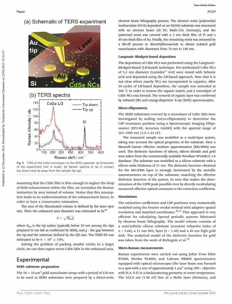
TERS measurements
Detection of fewer QDs as compared to SERS measurements wasachieved in a TERS experiment on the CdSe QD monolayer depos-ited on the SERS structure with 88 nm nanocluster diameter, whichis close to the resonance observed for the 632.8 nm excitation lineaccording to Fig. 4. Note that the shift of the resonance can becaused by the metallic tip when it approaches an Au nanocluster.The comparison of SERS and TERS spectra is shown in Fig. 5. In theTERS experiment, the area of the laser spot is approximately 1.5 �2.5 mm2, giving rise to the so-called far-field signal (tip up in Fig. 5b).When the electrochemically etched gold tip was brought into contactwith the QDs, the Raman signal from the QDs located directly underthe tip apex was enhanced (tip down in Fig. 5b). It was possible toachieve a 100% increase of the CdSe LO mode intensity at 207 cm�1.Similar to SERS spectra, the increased background at low frequencycan be attributed to enhancement of the signal from amorphous Seon the QD surface, and partially to elastic scattering from the tip.
The latter could lead to an increase of the Raman signal notrelated to the near-field enhancement.47,48 However, sincethe intensity of the Si peak remains the same, such a signalincrease can be excluded,39 and the TERS EF can be estimatedusing the formula:
EF ¼ Idown � Iup
Iup� Vill
Venh
where Idown (Iup) – intensity of the CdSe Raman signal with thetip down (up); Vill (Venh) – is the illuminated (enhanced) volume.
Fig. 3 Raman (black curve) and SERS (red curve) spectra of CdSe QDsmeasured with a 632.8 nm laser line for a nanocluster diameter of 80 nm.
Fig. 4 Normalized dependence of the Raman intensity of the CdSe LOphonon on the gold nanocluster diameter for different wavelengths(indicated in the figure).
PCCP Paper
Publ
ishe
d on
22
Dec
embe
r 20
14. D
ownl
oade
d by
Tec
hnis
che
Uni
vers
itat C
hem
nitz
on
25/0
1/20
15 1
2:31
:57.
View Article Online
Phys. Chem. Chem. Phys. This journal is© the Owner Societies 2015
Assuming that the CdSe film is thin enough to neglect the dropof field enhancement within the film, we normalize the Ramanintensities by area instead of volume. Notice that this assump-tion leads to an underestimation of the enhancement factor, inorder to have a conservative estimation.
The area of the illuminated volume is defined by the laser spotsize. Then the enhanced area diameter was estimated to be49
d ¼ffiffiffiffiffiffiffiffiffiffiRtipg
p
where Rtip is the tip radius (typically below 50 nm among the tipsprepared in our lab as confirmed by SEM), and g – the gap betweenthe tip and the substrate defined by the QD size. The TERS EF wasestimated to be 6 � 104 � 14%.
Solving the problem of packing smaller circles in a largercircle, we can then expect seven CdSe QDs in the enhanced area.
ExperimentalSERS substrate preparation
The 10� 10 mm2 gold nanocluster arrays with a period of 150 nmto be used as SERS substrates were prepared by a direct-write
electron beam lithography process. The electron resist (polymethylmethacrylate 950 K) deposited on an Si(100) substrate was structuredwith an electron beam (20 kV, Raith-150, Germany), and thepatterned resist was covered with a 5 nm thick film of Ti and a40 nm thick film of Au. Finally, the remaining resist was removed bya lift-off process in dimethylformamide to obtain isolated goldnanoclusters with diameters from 70 nm to 140 nm.
Langmuir–Blodgett-based deposition
The deposition of CdSe NCs was performed using the Langmuir–Blodgett-based (LB-based) technique. Pre-synthesized CdSe NCsof 5.2 nm diameter (Lumidott 610) were mixed with behenicacid and deposited using the LB-based approach. Note that it isnot clear where exactly NCs are incorporated in organics. After20 cycles of LB-based deposition, the sample was annealed at200 1C in order to remove the organic matrix, and a monolayer ofCdSe NCs was formed. The removal of organic layer was confirmedby infrared (IR) and energy-dispersive X-ray (EDX) spectroscopies.
Micro-ellipsometry
The SERS substrates covered by a monolayer of CdSe QDs wereinvestigated by nulling micro-ellipsometry to determine theLSP resonance position using a Spectroscopic Imaging Ellips-ometer (EP3-SE, Accurion GmbH) with the spectral range of365–1000 nm (3.4–1.24 eV).
The measured sample was modelled as a multi-layer system,taking into account the optical properties of the substrate. Here aMaxwell–Garnet effective medium approximation (MG-EMA) wasused. The dielectric functions of silicon, silicon dioxide and goldwere taken from the commercially available Woollam WVASE32 3.6database. The substrate was modelled as a silicon substrate with asilicon oxide thickness of 11 nm. The dielectric function obtainedfor the MG-EMA layer is strongly dominated by the metallicnanostructures on top of the substrate, matching the effectivedielectric function of the system. In turn this makes the deter-mination of the LSPR peak possible even by directly recalculatingmeasured effective optical constants to the extinction coefficient.
Simulations
The extinction coefficients and LSP positions were numericallymodeled using the Fourier modal method with adaptive spatialresolution and matched coordinates.40,41 This approach is veryefficient for calculating layered periodic systems fabricatedby electron beam lithography. The model volume consists ofa semi-infinite silicon substrate (constant refractive index ofn = 3.68), a 11 nm SiO2 layer (n = 1.46) and a 40 nm high golddisk. The analytical model of the dielectric function for goldwas taken from the work of Etchegoin et al.50
Micro-Raman measurements
Raman experiments were carried out using Jobin Yvon DilorXY800, Horiba T64000, and Labram HR800 spectrometersequipped with optical microscopes (the laser beam was focusedto a spot with a size of approximately 1 mm2 using 100� objectivewith N.A. 0.9) in a backscattering geometry at room temperature.The 632.8 nm (1.96 eV) line of a HeNe laser (Siemens), and
Fig. 5 TERS of the CdSe monolayer on the SERS substrate. (a) Schematicof the experiment (not in scale). (b) Raman spectra of tip in contact(tip down) and tip away from the sample (tip up).
Paper PCCP
Publ
ishe
d on
22
Dec
embe
r 20
14. D
ownl
oade
d by
Tec
hnis
che
Uni
vers
itat C
hem
nitz
on
25/0
1/20
15 1
2:31
:57.
View Article Online

This journal is© the Owner Societies 2015 Phys. Chem. Chem. Phys.
several lines of a Kr+ laser (Coherent) were used as excitationsources. A laser power below 1 mW was used in the experimentto avoid possible effects of local heating. For the SERS spectra(on Au nanocluster arrays) 10 s acquisition time, 15 accumulationswere performed; each Raman spectrum (on Si) was acquired for30 s, 60 accumulations, and the Raman intensity was divided by afactor of 3 in order to compare the intensities.
TERS measurements
For the TERS experiments, a Raman spectrometer (LabRam HR800)was coupled to an Agilent 5420 (Agilent, USA) atomic force micro-scope (AFM). A custom-made optical extension delivered the laserlight to the AFM tip at an angle of 701 with respect to the samplenormal axis. A 50� magnification long-working-distance objectivelens with N.A.0.42 (Mitutoyo, Japan) was used both to focus the laserlight onto the tip in the vicinity of the sample surface and to collectthe scattered light. The 632.8 nm laser line with a laser power of0.4 mW on the sample was used. The mirror and objective lens ofthe optical extension unit were driven by piezoelectric motors toimprove the system stability when aligning the laser on the tip.A fully metallic gold tip cantilever was used in contact mode inthe AFM for the TERS measurements. The cantilever preparationprocedure is described elsewhere.51 The tip apex was sharpened byelectrochemical etching. The TERS spectra were recorded with tipdown (in contact with the surface) and tip up (tip retracted by 1 mm)on the gold nanocluster array with a 150 nm period. The goldnanocluster diameter was 88 nm. The TERS spectra were accumu-lated for 5 s.
Conclusions
The LSPR positions of gold nanocluster arrays fabricated byelectron beam lithography were measured using spectroscopicmicro-ellipsometry and compared to values calculated using theFourier modal method. Both the experimental and the computa-tional approach show that the LSPR position red-shifts with anincrease in the nanocluster diameter. Using these SERS substrates,an enhancement factor as high as 2� 103 for the Raman scatteringby the CdSe LO phonon mode was demonstrated for a CdSe QDmonolayer. SERS allowed the detection of higher order phononmodes for CdSe QDs, demonstrating their remarkable crystallinequality. The dependence of SERS enhancement on the nanoclusterdiameter for different excitation wavelengths reveals a resonancebehaviour suggesting that the electromagnetic enhancementmechanism dominates. Finally, TERS results obtained from theCdSe QD monolayer on the SERS substrate allowed acquiring thespectrum of fewer QDs as compared to micro-Raman measure-ments with an additional enhancement on the order of 104. Thisopens up a prospective for studying phonon spectra of QD arrays ofa low areal density.
Acknowledgements
Authors thank DFG project ZA146/22-1, DFG Research Unit 1713SMINT, Russian Science Foundation (project 14-12-01037), and
Cluster of Excellence for Advanced Electronics Dresden (cfaed)for financial support. AM thanks DAAD for providing a scholar-ship. This work was performed in the context of the EuropeanCOST Action MP1302 Nanospectroscopy. M. N. acknowledgesfinancial support through an Alexander von Humboldt researchfellowship.
Notes and references
1 T. Trindade, P. O’Brien and N. L. Pickett, Chem. Mater.,2001, 13, 3843–3858.
2 L. J. Zhao, L. F. Hu and X. S. Fang, Adv. Funct. Mater., 2012,22, 1551–1566.
3 V. I. Klimov, A. A. Mikhailovsky, S. Xu, A. Malko, J. A.Hollingsworth, C. A. Leatherdale, H. J. Eisler and M. G.Bawendi, Science, 2000, 290, 314–317.
4 R. C. Somers, M. G. Bawendi and D. G. Nocera, Chem. Soc.Rev., 2007, 36, 579–591.
5 A. V. Uskov, A. P. Jauho, B. Tromborg, J. Mork and R. Lang,Phys. Rev. Lett., 2000, 85, 1516–1519.
6 A. J. Nozik, Annu. Rev. Phys. Chem., 2001, 52, 193–231.7 V. I. Klimov, D. W. McBranch, C. A. Leatherdale and M. G.
Bawendi, Phys. Rev. B: Condens. Matter Mater. Phys., 1999,60, 13740–13749.
8 D. A. Tenne, A. K. Bakarov, A. I. Toropov and D. R. T. Zahn,Phys. E, 2002, 13, 199–202.
9 D. A. Tenne, A. K. Bakarov, A. I. Toropov and D. R. T. Zahn,Phys. E, 2002, 13, 199–202.
10 J. Ibanez, A. Patane, M. Henini, L. Eaves, S. Hernandez,R. Cusco, L. Artus, Y. G. Musikhin and P. N. Brounkov, Appl.Phys. Lett., 2003, 83, 3069–3071.
11 J. Ibanez, R. Cusco, L. Artus, M. Henini, A. Patane andL. Eaves, Appl. Phys. Lett., 2006, 88, 141905.
12 A. Milekhin, A. Toropov, A. Kalagin and D. R. T. Zahn, Chin.J. Phys., 2011, 49, 71–76.
13 D. Cialla, A. Maerz, R. Boehme, F. Theil, K. Weber, M. Schmittand J. Popp, Anal. Bioanal. Chem., 2012, 403, 27–54.
14 J. Stadler, T. Schmid and R. Zenobi, Nanoscale, 2012, 4,1856–1870.
15 S. M. Nie and S. R. Emery, Science, 1997, 275, 1102–1106.16 K. Kneipp, Y. Wang, H. Kneipp, L. T. Perelman, I. Itzkan,
R. Dasari and M. S. Feld, Phys. Rev. Lett., 1997, 78, 1667–1670.17 R. Zhang, Y. Zhang, Z. C. Dong, S. Jiang, C. Zhang, L. G. Chen,
L. Zhang, Y. Liao, J. Aizpurua, Y. Luo, J. L. Yang and J. G. Hou,Nature, 2013, 498, 82–86.
18 W. Zhang, B. S. Yeo, T. Schmid and R. Zenobi, J. Phys. Chem.C, 2007, 111, 1733–1738.
19 M. D. Sonntag, J. M. Klingsporn, L. K. Garibay, J. M. Roberts,J. A. Dieringer, T. Seideman, K. A. Scheidt, L. Jensen, G. C. Schatzand R. P. Van Duyne, J. Phys. Chem. C, 2012, 116, 478–483.
20 J. T. Hugall, J. J. Baumberg and S. Mahajan, Appl. Phys. Lett.,2009, 95, 141111.
21 A. G. Milekhin, L. L. Sveshnikova, T. A. Duda, N. V. Surovtsev,S. V. Adichtchev and D. R. T. Zahn, JETP Lett., 2008, 88,799–801.
PCCP Paper
Publ
ishe
d on
22
Dec
embe
r 20
14. D
ownl
oade
d by
Tec
hnis
che
Uni
vers
itat C
hem
nitz
on
25/0
1/20
15 1
2:31
:57.
View Article Online

Phys. Chem. Chem. Phys. This journal is© the Owner Societies 2015
22 A. G. Milekhin, N. A. Yeryukov, L. L. Sveshnikova, T. A.Duda, S. S. Kosolobov, A. V. Latyshev, N. V. Surovtsev, S. V.Adichtchev, C. Himcinschi, E. I. Zenkevich, W.-B. Jian andD. R. T. Zahn, J. Phys. Chem. C, 2012, 116, 17164–17168.
23 A. G. Milekhin, N. A. Yeryukov, L. L. Sveshnikova, T. A. Duda,E. I. Zenkevich, S. S. Kosolobov, A. V. Latyshev, C. Himcinski,N. V. Surovtsev, S. V. Adichtchev, Z. C. Feng, C. C. Wu,D. S. Wuu and D. R. T. Zahn, J. Exp. Theor. Phys, 2011, 113,983–991.
24 N. A. Yeryukov, A. G. Milekhin, L. L. Sveshnikova, T. A.Duda, L. D. Pokrovsky, A. K. Gutakovskii, S. A. Batsanov,E. E. Rodyakina, A. V. Latyshev and D. R. T. Zahn, J. Phys.Chem. C, 2014, 118, 23409–23414.
25 D. O. Sigle, J. T. Hugall, S. Ithurria, B. Dubertret and J. J.Baumberg, Phys. Rev. Lett., 2014, 113, 087402.
26 N. Marquestaut, D. Talaga, L. Servant, P. Yang, P. Pauzauskie andF. Lagugne-Labarthet, J. Raman Spectrosc., 2009, 40, 1441–1445.
27 N. Kazemi-Zanjani, E. Kergrene, L. Liu, T.-K. Sham andF. Lagugne-Labarthet, Sensors, 2013, 13, 12744–12759.
28 Y. Ogawa, Y. Yuasa, F. Minami and S. Oda, Appl. Phys. Lett.,2011, 99, 053112.
29 M. Boehmler and A. Hartschuh, ChemPhysChem, 2012, 13,927–929.
30 M. Boehmler, Z. Wang, A. Myalitsin, A. Mews and A. Hartschuh,Angew. Chem., Int. Ed., 2011, 50, 11536–11538.
31 Y. Ogawa, T. Toizumi, F. Minami and A. V. Baranov, Phys.Rev. B: Condens. Matter Mater. Phys., 2011, 83, 081302(R).
32 W. Kiefer and S. Schlucker, Surface enhanced Raman spectro-scopy: analytical, biophysical and life science applications,John Wiley & Sons, 2013.
33 M. K. Fan, G. F. S. Andrade and A. G. Brolo, Anal. Chim. Acta,2011, 693, 7–25.
34 D. Cialla, A. Marz, R. Bohme, F. Theil, K. Weber, M. Schmittand J. Popp, Anal. Bioanal. Chem., 2012, 403, 27–54.
35 M. Kahl, E. Voges, S. Kostrewa, C. Viets and W. Hill, Sens.Actuators, B, 1998, 51, 285–291.
36 C. J. Choi, Z. Xu, H.-Y. Wu, G. L. Liu and B. T. Cunningham,Nanotechnology, 2010, 21, 415301.
37 R. Stosch, F. Yaghobian, T. Weimann, R. J. C. Brown,M. J. T. Milton and B. Guettler, Nanotechnology, 2011,22, 105303.
38 A. G. Milekhin, N. A. Yeryukov, L. L. Sveshnikova, T. A. Duda,E. E. Rodyakina, E. S. Sheremet, M. Ludemann, O. D. Gordan,A. V. Latyshev and D. R. T. Zahn, Thin Solid Films, 2013, 543,35–40.
39 E. Sheremet, R. D. Rodriguez, D. R. T. Zahn, A. G. Milekhin,E. E. Rodyakina and A. V. Latyshev, J. Vac. Sci. Technol., B:Nanotechnol. Microelectron.: Mater., Process., Meas., Phenom.,2014, 32, 04E110.
40 T. Weiss, N. A. Gippius, S. G. Tikhodeev, G. Granet andH. Giessen, J. Opt. Soc. Am. A, 2011, 28, 238–244.
41 T. Weiss, G. Granet, N. A. Gippius, S. G. Tikhodeev andH. Giessen, Opt. Express, 2009, 17, 8051–8061.
42 S. K. Islam, M. A. Sohel and J. R. Lombardi, J. Phys. Chem. C,2014, 118, 19415–19421.
43 B. K. Rai, H. D. Bist, R. S. Katiyar, M. T. S. Nair, P. K. Nairand A. Mannivannan, J. Appl. Phys., 1997, 82, 1310–1319.
44 Y. N. Hwang, S. H. Park and D. Kim, Phys. Rev. B: Condens.Matter Mater. Phys., 1999, 59, 7285–7288.
45 C. Trallero-Giner, A. Debernardi, M. Cardona, E. Menendez-Proupin and A. I. Ekimov, Phys. Rev. B: Condens. MatterMater. Phys., 1998, 57, 4664–4669.
46 A. A. Baganich, V. I. Mikla, D. G. Semak, A. P. Sokolov andA. P. Shebanin, Phys. Status Solidi B, 1991, 166, 297–302.
47 D. Roy, C. M. Williams and K. Mingard, J. Vac. Sci. Technol., B:Nanotechnol. Microelectron.: Mater., Process., Meas., Phenom.,2010, 28, 631–634.
48 N. Kumar, A. Rae and D. Roy, Appl. Phys. Lett., 2014,104, 123106.
49 I. Romero, J. Aizpurua, G. W. Bryant and F. J. Garcia deAbajo, Opt. Express, 2006, 14, 9988–9999.
50 P. G. Etchegoin, E. C. Le Ru and M. Meyer, J. Chem. Phys.,2006, 125, 164705.
51 R. D. Rodriguez, E. Sheremet, S. Mueller, O. D. Gordan,A. Villabona, S. Schulze, M. Hietschold and D. R. T. Zahn,Rev. Sci. Instrum., 2012, 83, 123708.
Paper PCCP
Publ
ishe
d on
22
Dec
embe
r 20
14. D
ownl
oade
d by
Tec
hnis
che
Uni
vers
itat C
hem
nitz
on
25/0
1/20
15 1
2:31
:57.
View Article Online