srs computer architecture - sydney russell school
TRANSCRIPT
GCE Computer Science
@ SRS
Computer Architecture Computer Systems
2020-21
1. INPUT & OUTPUT DEVICES
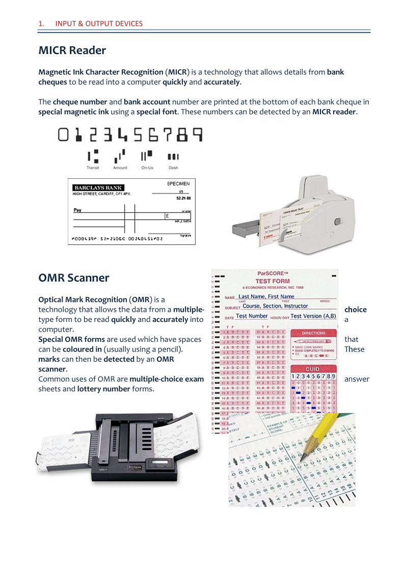
MICR Reader
Magnetic Ink Character Recognition (MICR) is a technology that allows details from bank cheques to be read into a computer quickly and accurately. The cheque number and bank account number are printed at the bottom of each bank cheque in special magnetic ink using a special font. These numbers can be detected by an MICR reader.
OMR Scanner
Optical Mark Recognition (OMR) is a technology that allows the data from a multiple- choice type form to be read quickly and accurately into a computer. Special OMR forms are used which have spaces that can be coloured in (usually using a pencil). These marks can then be detected by an OMR scanner. Common uses of OMR are multiple-choice exam answer sheets and lottery number forms.
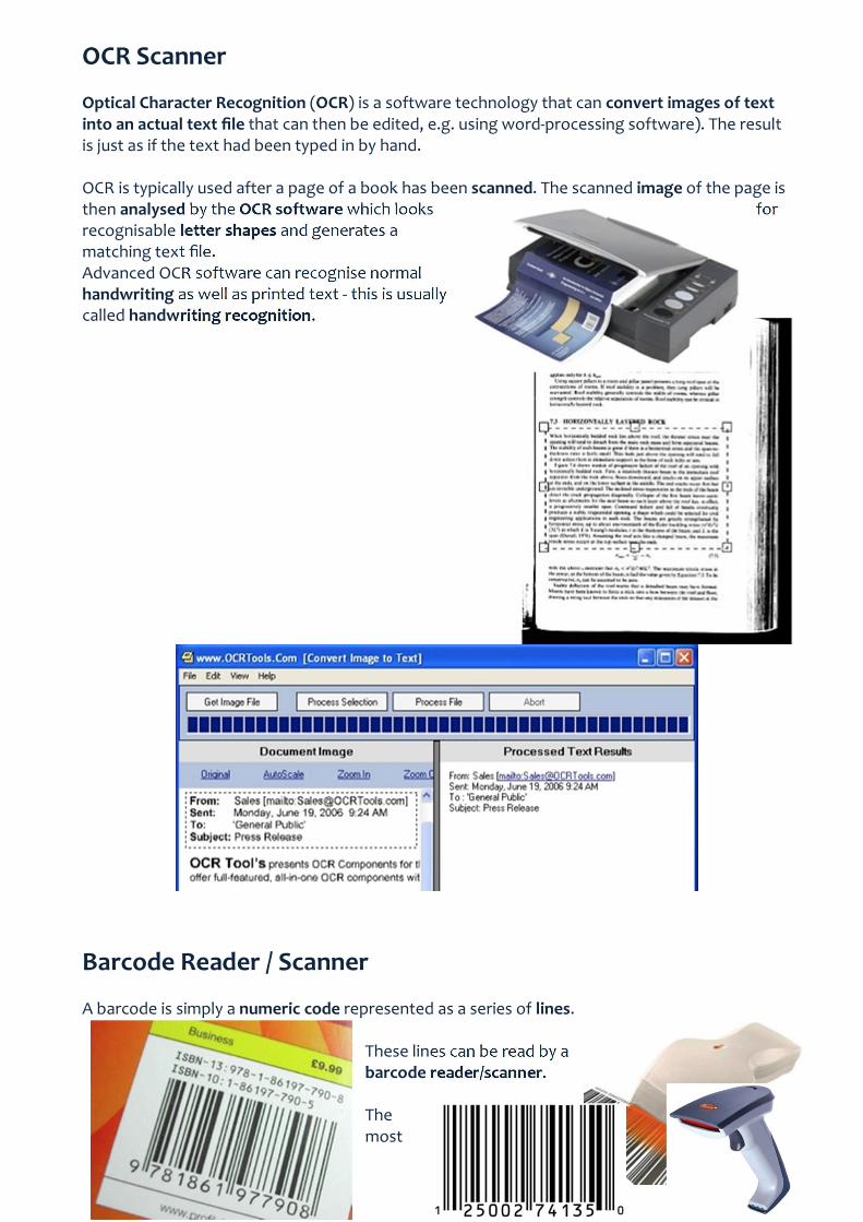
OCR Scanner
Optical Character Recognition (OCR) is a software technology that can convert images of text into an actual text file that can then be edited, e.g. using word-processing software). The result is just as if the text had been typed in by hand. OCR is typically used after a page of a book has been scanned. The scanned image of the page is then analysed by the OCR software which looks for recognisable letter shapes and generates a matching text file. Advanced OCR software can recognise normal handwriting as well as printed text - this is usually called handwriting recognition.
Barcode Reader / Scanner
A barcode is simply a numeric code represented as a series of lines. These lines can be read by a barcode reader/scanner. The most

common use of barcode readers is at Point-of-Sale (POS) in a shop. The code for each item to be purchased needs to be entered into the computer. Reading the barcode is far quicker and more accurate than typing in each code using a keypad. Barcode can be found on many other items that have numeric codes which have to be read quickly and accurately - for example ID cards.
Iden fy Uses for Input Devices
A blind student which uses the computer to complete his studies at home – What Input & Output Devices do you recommend and why? Input Devices
Output Devices
An underground sta on uses computers to sell ckets – What Input & Output Devices do you recommend and why? Input Devices
Output Devices
A plane pilot to control her plane – What Input & Output Devices do you recommend and why? Input Devices
Output Devices
A school canteen cashier – What Input & Output Devices do you recommend and why? Input Devices
Output Devices
A lo ery agent – What Input & Output Devices do you recommend and why? Input Devices
Output Devices
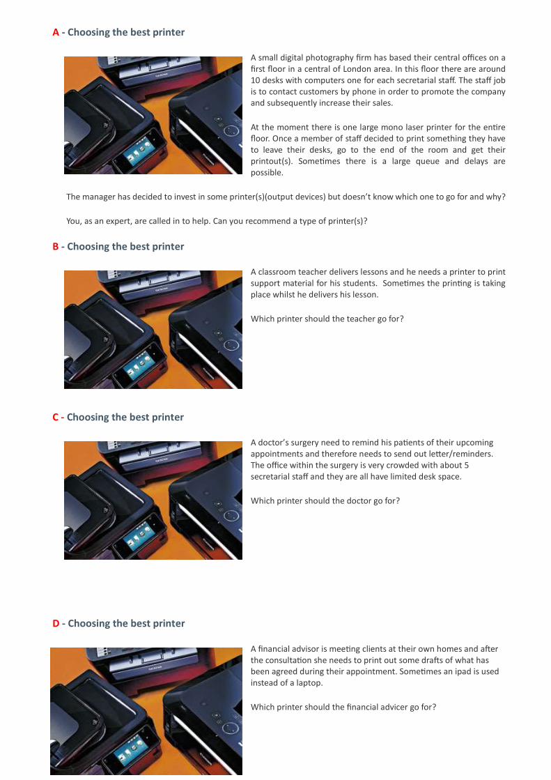
A - Choosing the best printer
A small digital photography firm has based their central offices on a first floor in a central of London area. In this floor there are around 10 desks with computers one for each secretarial staff. The staff job is to contact customers by phone in order to promote the company and subsequently increase their sales.
At the moment there is one large mono laser printer for the en re floor. Once a member of staff decided to print something they have to leave their desks, go to the end of the room and get their printout(s). Some mes there is a large queue and delays are possible.
The manager has decided to invest in some printer(s)(output devices) but doesn’t know which one to go for and why?
You, as an expert, are called in to help. Can you recommend a type of printer(s)?
B - Choosing the best printer
A classroom teacher delivers lessons and he needs a printer to print support material for his students. Some mes the prin ng is taking place whilst he delivers his lesson.
Which printer should the teacher go for?
C - Choosing the best printer
A doctor’s surgery need to remind his pa ents of their upcoming appointments and therefore needs to send out le er/reminders. The office within the surgery is very crowded with about 5 secretarial staff and they are all have limited desk space.
Which printer should the doctor go for?
D - Choosing the best printer
A financial advisor is mee ng clients at their own homes and a er the consulta on she needs to print out some dra s of what has been agreed during their appointment. Some mes an ipad is used instead of a laptop.
Which printer should the financial advicer go for?
Types of Printers
Inkjet printers
Mono Laser printers
All-in-one printers
Colour Laser printers
Wireless printers or Wired
Dot-Matrix
Plo ers
3D-Printers
Single User of Mul User
Selec ng a printer – Points to consider
Points to consider
Wireless or wired
All in One or single purpose
Colour Laser
Single User
Amount of prin ng
Mono Laser
Plo er
Mul User - Networking
Noise or quiet
Duplex prin ng
Speed of prin ng
Inkjet
Laser
Size of prin ng paper - envelope size, A4, A3, A1 etc.
Quality of prin ng – Photographs, normal paper, canvas etc.
Running Cost
Purchasing cost
Dot matrix: A type of impact printer that produces characters and illustra ons by striking pins against an ink ribbon to print closely spaced dots in the appropriate shape. Dot-matrix printers are rela vely expensive and do not produce high-quality output. However, they can print to mul -page forms (that is, carbon copies), something laser and ink-jet printers cannot do.
Ink-jet: A type of printer that works by spraying ionized ink at a sheet of paper. Magne zed plates in the ink's path direct the ink onto the paper in the desired shapes. Ink-jet printers are capable of producing high quality print approaching that produced by laser printers. A typical ink-jet printer provides a resolu on of 1200 dots per inch, although some newer models offer higher resolu ons. A typical ink-jet uses 1 black and 3 toner cartridges.
Laser: A type of printer that u lizes a laser beam to produce an image on a drum. The light of the laser alters the electrical charge on the drum wherever it hits. The drum is then rolled through a reservoir of toner, which is picked up by the charged por ons of the drum. Finally, the toner is transferred to the paper through a combina on of heat and pressure. This is also the way copy machines/photocopiers work. This is one of the fastest printers that is very economical when you produce many copies and provides very good quality output. It uses one black and 3 colour toners.
Plo ers: A printer that interprets commands from a computer to make line drawings on paper with one or more automated pens. Unlike a regular printer, the plo er can draw con nuous point-to-point lines. Plo ers were the first type of printer that could print with colour. As a rule, plo ers are much more expensive than printers. A plo er may use mul ple pens and pencils, which can be easily be changed out in order to create drawings of a different colour or drawings that contain more than one colour. A plo er is preferred over a printer in many commercial applica ons, including engineering, because it is far more exact.
It is because of this they are most frequently used for CAE (computer-aided engineering) applica ons, such as CAD (computer-aided design) and CAM (computer-aided manufacturing).
Wireless Printers: A printer is one kind of computer peripheral, a device that interacts with a computer and receives informa on from it, in this case, to create a hard copy of documents that exist in electronic form on the computer’s drive or a loca on accessed by the computer.
Like other peripherals, printers can be connected to the computer in various ways. Connec on methods have tradi onally included printer cables, USB cables, Ethernet cables, and more recently, wireless connec ons. Printers capable of connec ng wirelessly are referred to as wireless printers.
3D- Printers: 3D prin ng or addi ve manufacturing is a process of making three dimensional solid objects from a digital file. The crea on of a 3D printed object is achieved using addi ve processes. In an addi ve process an object is created by laying down successive layers of material un l the en re object is created.
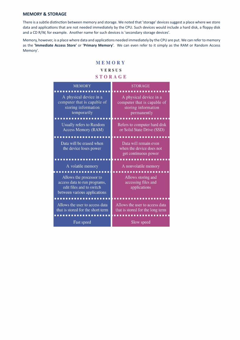
Storage Devices Magne c tape: A magne cally thin coated piece plas c wrapped around wheels capable of storing data. Tape is much less expensive than other storage mediums but commonly a much slower solu on that is commonly used for backup.
Today, tape has mostly been abandoned for faster and more reliable solu ons like disc drives, hard drives, and flash drives.
CD-ROM: Short for Compact Disc-Read Only Memory, CD-ROM drives or op cal drives are CD players inside computers that can have speeds in the range from 1x and beyond, and have the capability of playing audio CDs and computer data CDs. Below is a picture of the front and back of a standard CD-ROM drive. It is found as CD-R which means Read only. The spinning speed of the drive is affecc ng the bits per second that can be read at any me.
There are some DC’s that are known as cd writer, CD-WO (Write once), WORM (Write Once Read Many) drive. CD-R is short for CD-Recordable and is
a writable disc and drive that is capable of having informa on wri en to the disc once and then having that disc read many mes a er that.
Recordable DVD disks
Alterna vely referred to as a DVD writer, recordable DVD drives are disc drives capable of crea ng DVD discs. Unfortunately, unlike recordable CD drives, there are many different compe ng standards for crea ng DVD discs. For example, DVD-R, DVD-RW, DVD+R, DVD+RW, DVD+R DL (DVD+R9), and DVD-RAM are all different compe ng standards. Below is a brief explana on of each of these standards and related links to each of these standards.
USB Memory S ck
Alterna vely referred to as a USB flash drive, data s ck, pen drive, keychain drive and thumb drive, a jump drive is a portable drive that is o en the size of your thumb that connects to the com puter USB port. Today, flash drives are available in sizes such as 256MB, 512MB, 1GB, 5GB, and 16GB and are an easy way to transfer and store informa on.
In the picture to the right, is an example of the SanDisk Cruzer Micro 16GB flash drive and a good example of what many flash drives look like. As can be seen in this picture, the drive has a small casing that stores the flash memory connected to a USB connec on that is plugged into the USB port on your computer.
Magnetic hard disk:
Currently the most common type of secondary storage with very large capacities and good access speed.
The magnetic hard disk :
is reliable;
has a high capacity at low cost;
can be an internal device or external portable device for backup or transfer of large amounts of data;
stores the operating system, user data and programs.
Optical disk:
CD (compact disk) or DVD (digital versatile disk)
can be read only or read / write
CD/DVD ROM used to distribute programs
CD/DVD R/W used to store, transfer or backup data and program
o high capacity at low cost
o small and easy to distribute
o robust and can be used many times
o CD 700MB, DVD 4.7GB typical capacity
o slower than other media such as hard disk and flash ROM
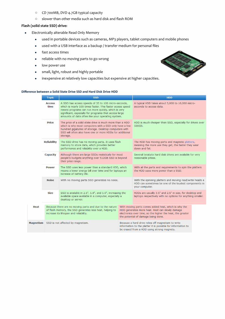
Flash (solid state SSD) drive:
Electronically alterable Read Only Memory
used in portable devices such as cameras, MP3 players, tablet computers and mobile phones
used with a USB interface as a backup / transfer medium for personal files
fast access times
reliable with no moving parts to go wrong
low power use
small, light, robust and highly portable
inexpensive at relatively low capacities but expensive at higher capacities.
Difference between a Solid State Drive SSD and Hard Disk Drive HDD
Magne c Storage Op cal Storage
a) Stores data in magne c form.
b) It is affected by magne c field.
c) It has high storage capacity.
e) It doesn't use laser to read/write data.
In your workbook write some examples of Magne c storage devices:
Magne c tape.
a) Stores data op cally & used laser to read/write.
b) It is not affected by magne c field.
c) It has less storage than magne c hard disk.
e) Data accessing is high as compared to magne c.
Write below some examples of Op cal storage devices:
Solid State Storage - 'No moving Parts' (SSD) Start-up faster due to no spin-up and they are faster than magne c hard drives They last longer and some are waterproof They are more robust as they haven't got any mechanical parts All data stored can be scanned quickly for security purposes
Write some examples of Solid State Storage:
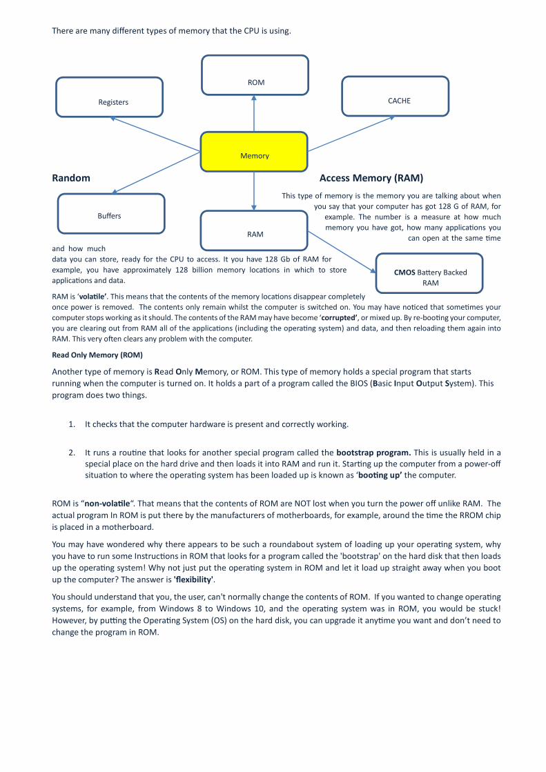
MEMORY & STORAGE
There is a subtle dis nc on between memory and storage. We noted that 'storage' devices suggest a place where we store data and applica ons that are not needed immediately by the CPU. Such devices would include a hard disk, a floppy disk and a CD R/W, for example. Another name for such devices is 'secondary storage devices'.
Memory, however, is a place where data and applica ons needed immediately by the CPU are put. We can refer to memory as the 'lmmediate Access Store' or 'Primary Memory'. We can even refer to it simply as the RAM or Random Access Memory'.
There are many different types of memory that the CPU is using.
Random Access Memory (RAM)
This type of memory is the memory you are talking about when you say that your computer has got 128 G of RAM, for
example. The number is a measure at how much memory you have got, how many applica ons you
can open at the same me and how much data you can store, ready for the CPU to access. It you have 128 Gb of RAM for example, you have approximately 128 billion memory loca ons in which to store applica ons and data.
RAM is ‘vola le’. This means that the contents of the memory loca ons disappear completely once power is removed. The contents only remain whilst the computer is switched on. You may have no ced that some mes your computer stops working as it should. The contents of the RAM may have become ‘corrupted’, or mixed up. By re-boo ng your computer, you are clearing out from RAM all of the applica ons (including the opera ng system) and data, and then reloading them again into RAM. This very o en clears any problem with the computer.
Read Only Memory (ROM)
Another type of memory is Read Only Memory, or ROM. This type of memory holds a special program that starts running when the computer is turned on. It holds a part of a program called the BIOS (Basic Input Output System). This program does two things.
1. It checks that the computer hardware is present and correctly working.
2. It runs a rou ne that looks for another special program called the bootstrap program. This is usually held in a
special place on the hard drive and then loads it into RAM and run it. Star ng up the computer from a power-off situa on to where the opera ng system has been loaded up is known as ‘boo ng up’ the computer.
ROM is “non-vola le“. That means that the contents of ROM are NOT lost when you turn the power off unlike RAM. The actual program In ROM is put there by the manufacturers of motherboards, for example, around the me the RROM chip is placed in a motherboard.
You may have wondered why there appears to be such a roundabout system of loading up your opera ng system, why you have to run some Instruc ons in ROM that looks for a program called the 'bootstrap' on the hard disk that then loads up the opera ng system! Why not just put the opera ng system in ROM and let it load up straight away when you boot up the computer? The answer is 'flexibility'.
You should understand that you, the user, can't normally change the contents of ROM. If you wanted to change opera ng systems, for example, from Windows 8 to Windows 10, and the opera ng system was in ROM, you would be stuck! However, by pu ng the Opera ng System (OS) on the hard disk, you can upgrade it any me you want and don’t need to change the program in ROM.
Memory
RAM
ROM
CMOS Ba ery Backed RAM
CACHE Registers
Buffers
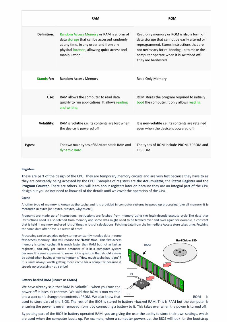
RAM ROM
Defini on: Random Access Memory or RAM is a form of data storage that can be accessed randomly at any me, in any order and from any physical loca on, allowing quick access and manipula on.
Read-only memory or ROM is also a form of data storage that cannot be easily altered or reprogrammed. Stores instruc ons that are not necessary for re-boo ng up to make the computer operate when it is switched off. They are hardwired.
Stands for: Random Access Memory Read Only Memory
Use: RAM allows the computer to read data quickly to run applica ons. It allows reading and wri ng.
ROM stores the program required to ini ally boot the computer. It only allows reading.
Vola lity: RAM is vola le i.e. its contents are lost when the device is powered off.
It is non-vola le i.e. its contents are retained even when the device is powered off.
Types: The two main types of RAM are sta c RAM and dynamic RAM.
The types of ROM include PROM, EPROM and EEPROM.
Registers
These are part of the design of the CPU. They are temporary memory circuits and are very fast because they have to as they are constantly being accessed by the CPU. Examples of registers are the Accumulator, the Status Register and the Program Counter. There are others. You will learn about registers later on because they are an Integral part of the CPU design but you do not need to know all of the details un l we cover the opera on of the CPU.
Cache
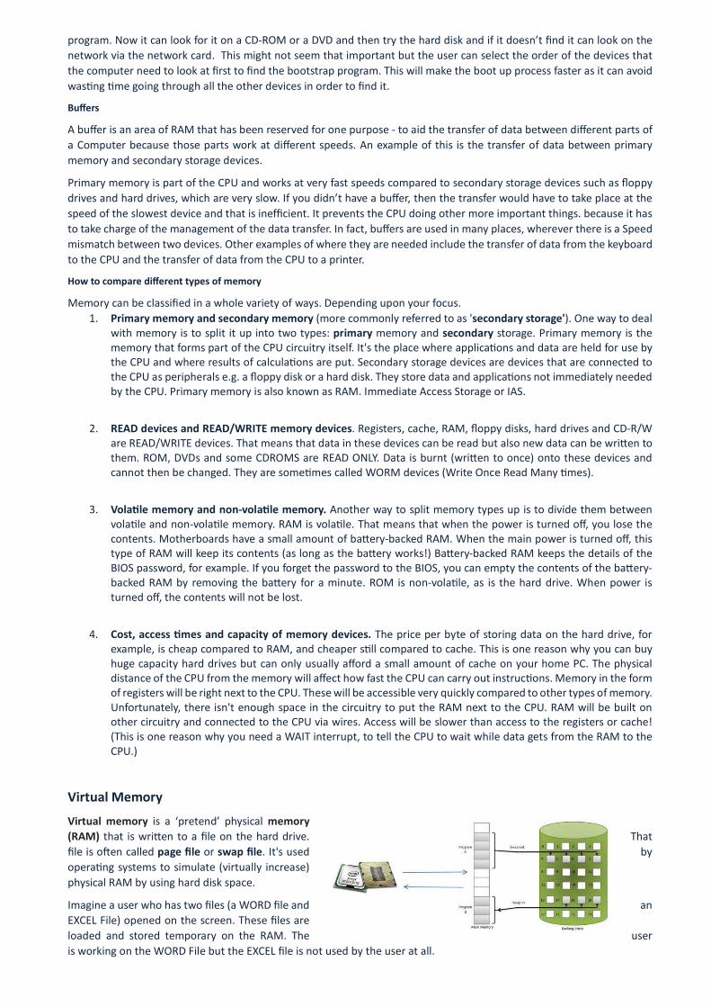
Another type of memory is known as the cache and it Is provided in computer systems to speed up processing. Like all memory, it Is measured in bytes (or Kbytes. Mbytes, Gbytes etc.).
Programs are made up of instruc ons. Instruc ons are fetched from memory using the fetch-decode-execute cycle The data that instruc ons need Is also fetched from memory and some data might need to be fetched over and over again for example, a constant that Is held in memory and used lots of mes in lots of calcula ons. Fetching data from the Immediate Access store takes me. Fetching the same data a er me is a waste of me!
Processing can be speeded up by storing constantly-needed data in some fast-access memory. This will reduce the 'fetch' me. This fast-access memory Is called 'cache'. It is much faster than RAM but not as fast as registers). You only get limited amounts of It in a computer system because It is very expensive to make. One ques on that should always be asked when buying a new computer is "How much cache has it got"? It is usual always worth ge ng more cache for a computer because it speeds up processing - at a price!
Ba ery-backed RAM (known as CMOS)
We have already said that RAM is ‘vola le’ – when you turn the power off it loses its contents. We said that ROM is non-vola le and a user can’t change the contents of ROM. We also know that ROM is used to store part of the BIOS. The rest of the BIOS is stored in ba ery –backed RAM. This is RAM but the computer is ensuring the power is never removed from it by connec ng a ba ery to it. This takes over when the power is turned off.
By pu ng part of the BIOS in ba ery operated RAM, you ae giving the user the ability to store their own se ngs, which are used when the computer boots up. For example, when a computer powers up, the BIOS will look for the bootstrap
L1
L2
RAM
program. Now it can look for it on a CD-ROM or a DVD and then try the hard disk and if it doesn’t find it can look on the network via the network card. This might not seem that important but the user can select the order of the devices that the computer need to look at first to find the bootstrap program. This will make the boot up process faster as it can avoid was ng me going through all the other devices in order to find it.
Buffers
A buffer is an area of RAM that has been reserved for one purpose - to aid the transfer of data between different parts of a Computer because those parts work at different speeds. An example of this is the transfer of data between primary memory and secondary storage devices.
Primary memory is part of the CPU and works at very fast speeds compared to secondary storage devices such as floppy drives and hard drives, which are very slow. If you didn’t have a buffer, then the transfer would have to take place at the speed of the slowest device and that is inefficient. It prevents the CPU doing other more important things. because it has to take charge of the management of the data transfer. In fact, buffers are used in many places, wherever there is a Speed mismatch between two devices. Other examples of where they are needed include the transfer of data from the keyboard to the CPU and the transfer of data from the CPU to a printer.
How to compare different types of memory
Memory can be classified in a whole variety of ways. Depending upon your focus. 1. Primary memory and secondary memory (more commonly referred to as 'secondary storage'). One way to deal
with memory is to split it up into two types: primary memory and secondary storage. Primary memory is the memory that forms part of the CPU circuitry itself. It's the place where applica ons and data are held for use by the CPU and where results of calcula ons are put. Secondary storage devices are devices that are connected to the CPU as peripherals e.g. a floppy disk or a hard disk. They store data and applica ons not immediately needed by the CPU. Primary memory is also known as RAM. Immediate Access Storage or IAS.
2. READ devices and READ/WRITE memory devices. Registers, cache, RAM, floppy disks, hard drives and CD-R/W
are READ/WRITE devices. That means that data in these devices can be read but also new data can be wri en to them. ROM, DVDs and some CDROMS are READ ONLY. Data is burnt (wri en to once) onto these devices and cannot then be changed. They are some mes called WORM devices (Write Once Read Many mes).
3. Vola le memory and non-vola le memory. Another way to split memory types up is to divide them between
vola le and non-vola le memory. RAM is vola le. That means that when the power is turned off, you lose the contents. Motherboards have a small amount of ba ery-backed RAM. When the main power is turned off, this type of RAM will keep its contents (as long as the ba ery works!) Ba ery-backed RAM keeps the details of the BIOS password, for example. If you forget the password to the BIOS, you can empty the contents of the ba ery-backed RAM by removing the ba ery for a minute. ROM is non-vola le, as is the hard drive. When power is turned off, the contents will not be lost.
4. Cost, access mes and capacity of memory devices. The price per byte of storing data on the hard drive, for
example, is cheap compared to RAM, and cheaper s ll compared to cache. This is one reason why you can buy huge capacity hard drives but can only usually afford a small amount of cache on your home PC. The physical distance of the CPU from the memory will affect how fast the CPU can carry out instruc ons. Memory in the form of registers will be right next to the CPU. These will be accessible very quickly compared to other types of memory. Unfortunately, there isn't enough space in the circuitry to put the RAM next to the CPU. RAM will be built on other circuitry and connected to the CPU via wires. Access will be slower than access to the registers or cache! (This is one reason why you need a WAIT interrupt, to tell the CPU to wait while data gets from the RAM to the CPU.)
Virtual Memory
Virtual memory is a ‘pretend’ physical memory (RAM) that is wri en to a file on the hard drive. That file is o en called page file or swap file. It's used by opera ng systems to simulate (virtually increase) physical RAM by using hard disk space.
Imagine a user who has two files (a WORD file and an EXCEL File) opened on the screen. These files are loaded and stored temporary on the RAM. The user is working on the WORD File but the EXCEL file is not used by the user at all.
The CPU in order to release space so it can store other instruc ons which are needed on RAM, temporary removes the EXCEL File from its loca on in RAM into another area inside the HARD disk. The CPU now has more space in RAM to place other current instruc ons.
When the user decides to work on the EXCEL file the CPU will request it from the HARD DISK. In the mean me, the WORD file from RAM will now be placed in the HARD DISK area and the EXCEL FILE will now take place inside the RAM. The two
files have now swapped posi on.
The CPU decides where about these files are stored in the hard disk so it can retrieve them later on.
This process allows the CPU to have more RAM space when it is needed. The Primary memory RAM can double in size by making use of this addi onal memory known as VIRTUAL MEMORY. Remember Virtual is not physical memory.
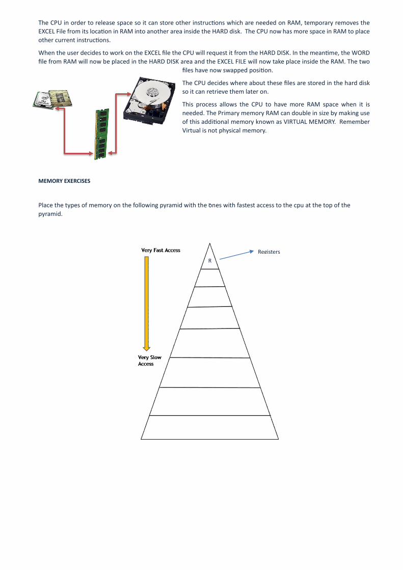
MEMORY EXERCISES
Place the types of memory on the following pyramid with the ones with fastest access to the cpu at the top of the pyramid.
R
Registers R
Motherboard
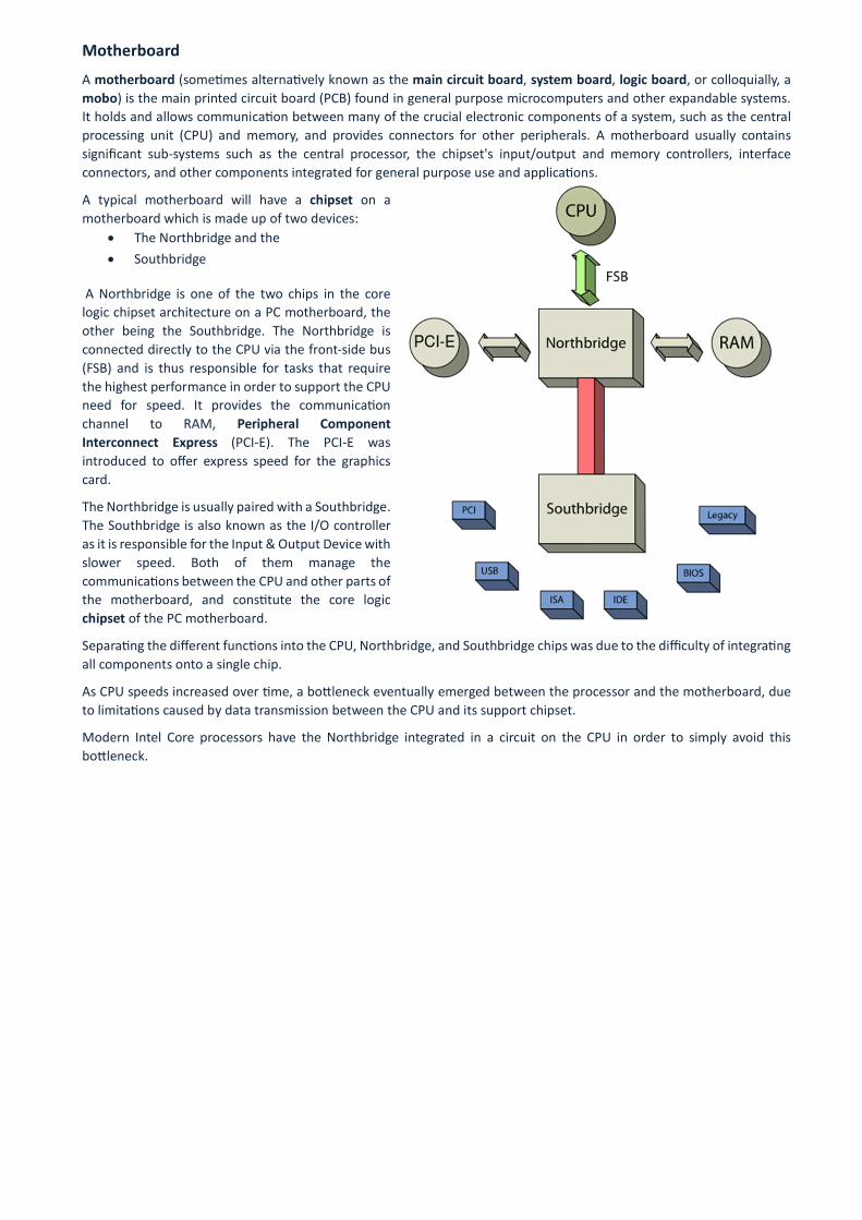
A motherboard (some mes alterna vely known as the main circuit board, system board, logic board, or colloquially, a mobo) is the main printed circuit board (PCB) found in general purpose microcomputers and other expandable systems. It holds and allows communica on between many of the crucial electronic components of a system, such as the central processing unit (CPU) and memory, and provides connectors for other peripherals. A motherboard usually contains significant sub-systems such as the central processor, the chipset's input/output and memory controllers, interface connectors, and other components integrated for general purpose use and applica ons.
A typical motherboard will have a chipset on a motherboard which is made up of two devices:
The Northbridge and the Southbridge
A Northbridge is one of the two chips in the core logic chipset architecture on a PC motherboard, the other being the Southbridge. The Northbridge is connected directly to the CPU via the front-side bus (FSB) and is thus responsible for tasks that require the highest performance in order to support the CPU need for speed. It provides the communica on channel to RAM, Peripheral Component Interconnect Express (PCI-E). The PCI-E was introduced to offer express speed for the graphics card.
The Northbridge is usually paired with a Southbridge. The Southbridge is also known as the I/O controller as it is responsible for the Input & Output Device with slower speed. Both of them manage the communica ons between the CPU and other parts of the motherboard, and cons tute the core logic chipset of the PC motherboard.
Separa ng the different func ons into the CPU, Northbridge, and Southbridge chips was due to the difficulty of integra ng all components onto a single chip.
As CPU speeds increased over me, a bo leneck eventually emerged between the processor and the motherboard, due to limita ons caused by data transmission between the CPU and its support chipset.
Modern Intel Core processors have the Northbridge integrated in a circuit on the CPU in order to simply avoid this bo leneck.
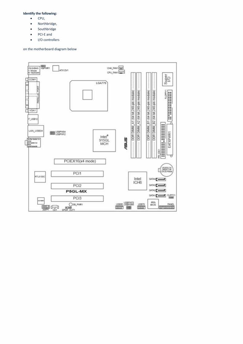
Iden fy the following: CPU, Northbridge, Southbridge PCI-E and I/O controllers
on the motherboard diagram below
TASK 1 - Describe and compare exactly what kind of data each of the following types of memory hold:
a. RAM
b. ROM
c. registers
d. cache
e. ba ery-backed RAM
TASK 2 - Explain the terms 'vola le' and 'non-vola le' when applied to memory.
TASK 3 - What is the purpose of the 'bootstrap program"?
TASK 4 - Explain what is meant by ‘boo ng up a computer'.
TASK 5 - Explain why re-boo ng a computer o en sorts out so ware problems.
TASK 6 - How many bytes are there in 256 Mbytes? You should give:
a) an approximate answer and
b) an exact answer.
TASK 7 - What does BIOS stand for?
TASK 8 - Explain why the opera ng system on a PC is not held in ROM.
TASK 9 - Describe how providing cache to a computer system without any should improve performance.
TASK 10 - Describe the purpose of ba ery-backed RAM.
TASK 11 - Explain with the aid of an example the problem of 'speed mismatch‘ between two devices and describe how the computer overcomes this.
Glossary Primary Memory
There are two types of primary memory, ROM and RAM. Any other type of storage (such as magnetic, optical, or solid-state media) is secondary storage. Data stored in secondary storage cannot be accessed by the processor until it is moved to RAM.
Read Only Memory (ROM)
Read Only Memory, or ROM, is where data that is vital to the operation of the computer, such as BIOS and UEFI, because it cannot be deleted, altered, or tampered with. The main disadvantage of this is that the software stored in ROM cannot be upgraded or updated.
Random Access Memory (RAM)
RAM stores the programs that are being used by the computer (including the operating system). RAM is volatile memory, as any data stored in it is lost when the computer is switched off, or loses power.
Secondary Storage
Secondary storage is where data is stored that does not need to be accessed by the processor. It is generally far larger than primary storage - a powerful computer might have 16GB of primary memory, but 2,000GB of secondary storage. Secondary storage is also non-volatile, which is good, otherwise every time there is a power cut, or the computer gets turned off, all the data stored on the computer would be lost (except the ROM).
Op cal
Optical media is popular because it is relatively cheap, and it is very reliable, and can be dropped and mistreated with no ill effects, as long as the surface of the disc is protected. Data is stored on optical media using "pits" (binary 0) and "land" (binary 1), and is read using a laser. CDs, DVDs, and Blu-Ray discs are all examples of optical media. Most optical media is read-only, however it can sometimes be rewritten, for example CD-RWs.
A disc refers to optical media, but a disk refers to magnetic media!
Magne c
Broadly speaking, there are two types of magnetic media - tape and disks. Tape is mainly used for archiving, as it takes a long time to "seek" between two sections of tape. Hard disks are mainly used for long term data storage, where speed is also important, for example the storage of hundreds of high-quality movies on a computer. Hard disks are read using a "head", which skims the surface of several "platters", or disks. These are all encased in one sealed unit. Hard drives are faster than tape and optical media, but slower than a solid state drive.
Solid-state
Solid state storage is generally divided into two categories - "slow" storage (such as a flash drive), and "fast" storage (such as an SSD). All solid state storage is very good at dealing with small files, as no movement is required to "find" (seek) files, like with magnetic or optical storage. However, SSD's are fast enough to replace a traditional hard drive, as they can be 4 or 5 times faster than a spinning hard drive. (A flash drive can also be used to replace a hard drive, however flash drives can be 20 times slower than hard drives, even though they can seek faster).
Data Transfer
Data can either be stored in primary memory or secondary storage. However, sometimes data needs to be moved, for example, because the computer is about to be switched off, and anything in volatile memory (such as RAM) will be lost, or if the processor wants to work with some data, which is currently stored in secondary storage (but needs to be stored in primary storage for the processor to use it). Because the memory controller (which controls primary memory - RAM in this case) is part of the processor, the data has to be copied from secondary storage to the ALU (or vice versa).
However, we know that the ALU is extremely fast, compared with primary storage which is (relatively speaking) slow. This means that the processor will be waiting time waiting for secondary storage, when it should be processing something else. The solution is to have a buffer, which fills up. When it is full, an "interrupt" is sent to the processor, and the data in the buffer is transferred to the ALU, and then to primary memory. The same system works in the opposite way when transferring data from primary memory to secondary storage.
Applica ons So ware - so ware which helps the user complete specific tasks - for example word processing.
Archive - informa on is archived if it doesn't need to be accessed frequently, but it may need to be accessed at some point in the future. For example, student records a er students have le the school - if the student later asks for a reference, then the school would have to retrieve their student record from the archive.
Basic Input Output System (BIOS) - where important instruc ons explaining how to turn on the computer are stored - for example, how to find a keyboard and interpret keystrokes.
Bit - a binary 1 or 0. Bits are normally part of a byte.
Bitrate - the amount of data (measured in bits) that can be transmi ed per second. Can also be called the baud rate.
Byte - a group of bits (usually 8) treated as one unit.
Checksum - an extra byte that is added to a block of data, which is the sum of the bits, ignoring any carry. This is then calculated by the receiver, and if the checksums match, then the data is accepted.
Duplex - where data can travel in both direc on at the same me - e.g. ethernet.
Echo (Error Checking) - when data is sent, a copy is then returned to the sender, to check it is the same data as the sender sent.
Error (Data Transmission) - where data is corrupted (changed) while being transferred from one place to another. See 1.5.4 Error Checking.
Ethernet - a cable standard used to connect nodes within a LAN.
Graphical User Interface (GUI) - an intui ve interface using images to represent commands. It is easy for beginners to use; however, it can be slow as many commands are hidden so the user is not confused.
Half Duplex - where data can travel in both direc ons, but only in one direc on at a me - e.g. a walkie-talkie.
Handshake - before two devices can communicate, they must ensure they are both ready to communicate, and agree the protocols to be used, by comple ng a "handshake".
Hardware - the physical components which make up the computer. Hardware hurts if you are hit over the head with it.
Input Device - a type of peripheral that can accept data, decode it, and send it as electrical pulses to the computer. For example: keyboards, mice, digital cameras, and microphones.
I/O Device - a device that communicates between the computer and the outside word - for example a keyboard or a printer. Some mes also known as an HID (Human Interface Device).
Local Area Network (LAN) - computers connected to each other in a geographically small area, for example a home network.
Magne c Ink Character Reader (MICR) - reads characters which have been printed using special magne c ink. The only common use for MICR is the account informa on printed on the bo om of cheques. Unlike barcodes, MICR can easily be read by both humans and computers.
Network - 2 or more compu ng devices connected together so that they can share data and resources.
Network Interface Card (NIC) - an expansion card that allows a computer to connect to a network. Most motherboards have wired (ethernet) NIC's built in, but an expansion card might be required for wireless access.
Node - a piece of equipment, such as a PC or peripheral, a ached to a network.
Op cal Character Recogni on (OCR) - converts text on paper to digital characters, by comparing a scanned character with a database. Works best on typed pages, but also works with handwri ng.
Op cal Mark Reader (OMR) - recognizes marks on a sheet of paper. Commonly used in mul ple choice exams, or on lo ery ckets.
Output Device - a device that turns computer signals into a human-readable form, like a screen, printer, or speaker.
Packet - a group of bytes for network transmission. Each packet has a unique ID (a label), a sequence number, a des na on address, and a checksum.
Parallel (Data Transmission) - using many wires, each transferring a bit at the same me (e.g. 8 wires to transfer an en re byte of 8 bits).
Parity Checking - a method used for error checking, where it is agreed that the number of bits will be odd or even. 7 bits of the byte are used for actual data, and one of the bits is used to ensure the parity is correct. See 1.5.4 Error Checking.
Peripheral - a device that is connected to a host computer, but not part of it. For example, a webcam or a graphics card would be a peripheral, as they are not required for a computer to operate. However, a power supply would not be a peripheral, as a computer would not func on without one. Although RAM is technically a peripheral, removing it will effec vely disable any modern machine, therefore it is a primary component.
Primary Component - a piece of hardware which is cri cal for a computer to work. For example, a CPU, or a power supply.
Primary Memory - ROM and RAM.
Protocol - a set of rules governing the transmission of data. There are two types of protocol - logical protocols (rela ng to so ware) and physical protocols (rela ng to hardware).
Random Access Memory (RAM) - used to store short term informa on - e.g. when browsing the internet, web pages might be downloaded and stored in RAM. It's name is derived from the fact that random storage loca ons can all be accessed quickly (less than 1ms) - in contrast to tradi onal hard disks, which can take up to 10 milliseconds due to mechanical limita ons. RAM is vola le memory, so it can only be used for short term storage.
Read Only Memory (ROM) - used to store data that should never be altered, for example the BIOS or UEFI. Informa on stored in ROM cannot be altered, deleted, or otherwise interfered with.
Serial (Data Transmission) - where each of the 8 bits is transmi ed down a single wire connec on one at a me.
Simplex - data is only ever able to travel in one direc on - e.g. from a radio sta on to a radio.
So ware - the instruc ons and code that tells the computer what to do. There are two types of so ware, applica ons so ware and system so ware.
Sta c State Drive (SSD) - a replacement for hard drives. An SSD is smaller and faster than a hard drive which costs the same amount. Typically, the opera ng system is stored on an SSD, while large files such as photos, music, and videos, are stored on a "tradi onal" spinning hard disk.
Standalone - a computer which is not connected to other computers.
Storage Device - a memory device used to store opera ng systems, programs, and user data. Storage devices are non-vola le - they do not lose their data when they are unpowered. See 1.4.3 Memory and Storage.
Syntax - the par cular rules of a given programming language. For example, surrounding strings in quotes (either single or double quotes) is a syntax rule for python.
System So ware - system so ware provides basic func onality, such as file management, or providing a Graphical User Interface.
Unified Extensible Firmware Interface (UEFI) - a modern replacement for BIOS, which will reduce the me it takes for computers to start up. This is because it can be accessed through opera ng systems, such as Microso Windows. It also supports "modern" features, such as a mouse, making it more user-friendly.
Vola le Memory - memory which gets lost when the power is turned off.
Wide Area Network (WAN) - computers connected to each other over a geographically large area, for example the internet.
2. NUMBER SYSTEMS – CHARACTER SETS
Character Set
The computers only understand two sets of values 1 (ON) and 0 (OFF). The computer is made up of a series of switches that can be turned ON or OFF. When you press a key on the keyboard a code is generated. This code is then translated into a number of switches that are turned ON or OFF. To represent this code we use bits (binary digits).
A character set is basically a way of expressing text (le ers, numbers, commands and symbols) as binary digits (bits). In the 1960s, computers all used different character sets, so it was hard to make them communicate. Manufacturers realised this was a problem, so they had a mee ng in America, and created a set of codes called ASCII (American Standard Code for Informa on Interchange - pronounced ass-key). To represent all 128 ASCII characters, we need a 7 - bit representa on as the 27 = 128. Later on it was extended and it is now known as an Extended ASCII with an 8-bit representa on. 28 = 256 characters are enough to represent all other characters from France, Germany etc.
ASCII isn't the only character set - there are others, such as EBCDIC, which was used on IBM machines, and is based on Binary Coded Decimal, and UNICODE, which is similar to ASCII, but represents far more characters, including Arabic, Chinese, and Japanese characters.
People enter data into a computer by means of an input device such as a keyboard. But actually a keyboard is simply a set of switches arranged in a certain way for your convenience. Every key is physically iden cal - there is no 'le er A' key or 'le er X' key.
What happens is that the keyboard sends a signal to the computer that effec vely says 'The third key on the middle row has been pressed'. This 'signal' is a combina on of switches which are turned ON or OFF in order to produce a binary number that represents it.
The computer then has to work out what this actually means, so there has to be a transla on between the 'third key signal' and what needs to appear on the screen. This is the job of the 'character set'.
“A character set converts a binary number / code into a wri en language character”.
For example, if you use a European language keyboard then the "La n Alphabet No 1" character set may be installed on the computer to translate the keys into the right language symbols for you (there are other character sets that would also do the same job).
A completely different language such as Japanese would use a different character set and of course the middle-row third key would have a different symbol on it.
Do not confuse character set with font. They are not the same thing. A font will display the le er 'A' in a certain way - but it is s ll the le er A no ma er how fancy the font!
It is the character set that maps a binary code to the le er A whatever font you have selected will then be display it in certain way.
So far, we have discussed 1 byte character sets such as ASCII and extended ASCII. But these can only describe 256 symbols. Some languages have far more than this. For instance some far-east languages have more than 12,000 characters!
So the logical way of handling the problem is to use a character set that uses more than 8 bits (1 byte).
0 1 0 1 0 1 0 0
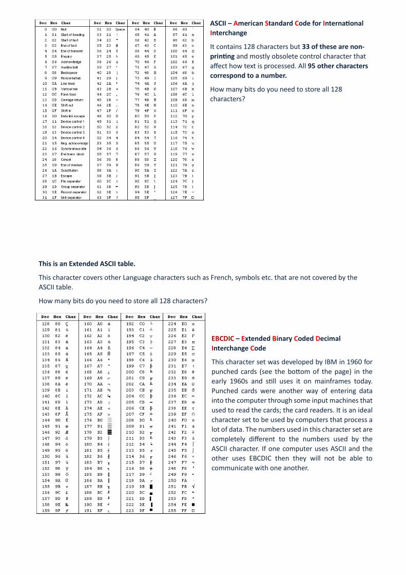
ASCII – American Standard Code for Interna onal Interchange
It contains 128 characters but 33 of these are non-prin ng and mostly obsolete control character that affect how text is processed. All 95 other characters correspond to a number.
How many bits do you need to store all 128 characters?
This is an Extended ASCII table.
This character covers other Language characters such as French, symbols etc. that are not covered by the ASCII table.
How many bits do you need to store all 128 characters?
EBCDIC – Extended Binary Coded Decimal Interchange Code
This character set was developed by IBM in 1960 for punched cards (see the bo om of the page) in the early 1960s and s ll uses it on mainframes today. Punched cards were another way of entering data into the computer through some input machines that used to read the cards; the card readers. It is an ideal character set to be used by computers that process a lot of data. The numbers used in this character set are completely different to the numbers used by the ASCII character. If one computer uses ASCII and the other uses EBCDIC then they will not be able to communicate with one another.
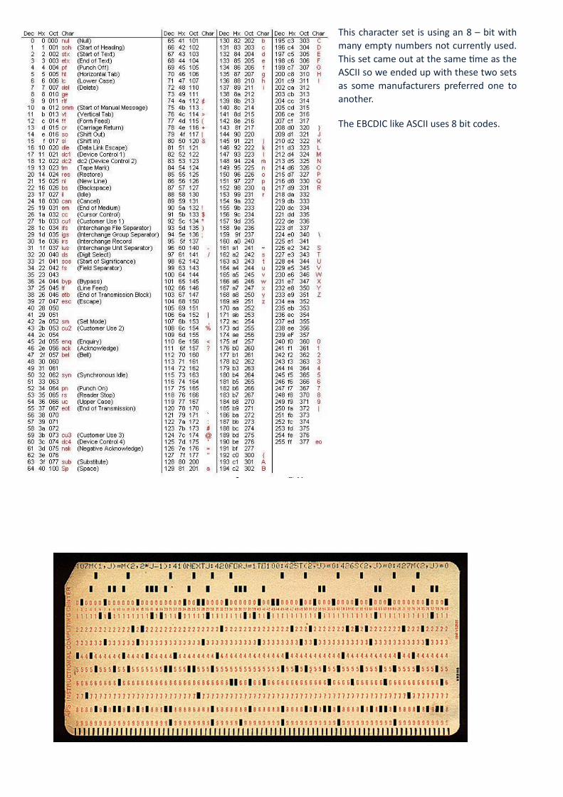
This character set is using an 8 – bit with many empty numbers not currently used. This set came out at the same me as the ASCII so we ended up with these two sets as some manufacturers preferred one to another.
The EBCDIC like ASCII uses 8 bit codes.
Unicode
As the Extended ASCII only covers 256 characters there is a need for a larger set to include other characters from other languages as well. Unicode is another character set which uses a 16 bit code (twice the bits used for ASCII) and represents over 65000 characters. With this set you have the ability to represent all the wri ng systems of the world; languages such as Chinese, Japanese, Arabic and even ancient languages such as Egyp an, La n or Ancient Greek. Microso and Apple both support the use of Unicode for their opera ng systems.
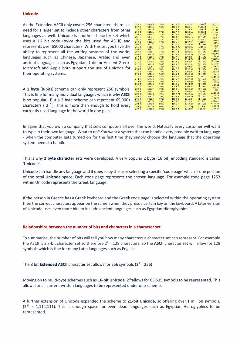
A 1 byte (8-bits) scheme can only represent 256 symbols. This is fine for many individual languages which is why ASCII is so popular. But a 2 byte scheme can represent 65,000+ characters ( 216 ). This is more than enough to hold every currently used language in the world in one place.
Imagine that you own a company that sells computers all over the world. Naturally every customer will want to type in their own language. What to do? You want a system that can handle every possible wri en language - when the computer gets turned on for the first me they simply choose the language that the opera ng system needs to handle.
This is why 2 byte character sets were developed. A very popular 2 byte (16 bit) encoding standard is called 'Unicode'.
Unicode can handle any language and it does so by the user selec ng a specific 'code page' which is one por on of the total Unicode space. Each code page represents the chosen language. For example code page 1253 within Unicode represents the Greek language.
If the person in Greece has a Greek keyboard and the Greek code page is selected within the opera ng system then the correct characters appear on the screen when they press a certain key on the keyboard. A later version of Unicode uses even more bits to include ancient languages such as Egyp an Hieroglyphics.
Rela onships between the number of bits and characters in a character set
To summarise, the number of bits will tell you how many characters a character set can represent. For example the ASCII is a 7-bit character set so therefore 27 = 128 characters. So the ASCII character set will allow for 128 symbols which is fine for many La n languages such as English.
The 8 bit Extended ASCII character set allows for 256 symbols (28 = 256)
Moving on to mul -byte schemes such as 16-bit Unicode, 216allows for 65,535 symbols to be represented. This allows for all current wri en languages to be represented under one scheme.
A further extension of Unicode expanded the scheme to 21-bit Unicode, so offering over 1 million symbols, (221 = 1,114,111). This is enough space for even dead languages such as Egyp an Hieroglyphics to be represented.
Q1. Explain what is meant by the character set of a computer.
…………………………………………………………………………………………………………………………………………………………………………
…………………………………………………………………………………………………………………………………………………………………………
…………………………………………………………………………………………………………………………………………………………………………
……………………………………………………………………………………………………..…………………………………………………………………
…………………………………………..……………………………..……………………………..……………………………………………[2]
Q2. By referring to two examples of applications that need character sets of different sizes, explain how codes are used to represent character sets.
…………………………………………………………………………………………………………………………………………………………………………
…………………………………………………………………………………………………………………………………………………………………………
…………………………………………………………………………………………………………………………………………………………………………
……………………………………………………………………………………………………..……………………………..……………………………..……
…………………….……………………..……………………………..……………………………..……………………………..…..[1,1,2]
Q3. A car insurance firm collects data from its customers and stores it on a computer. The customer name is
stored using the computers character set. Explain what is meant by the character set of a computer.
…………………………………………………………………………………………………………………………………………………………………………
…………………………………………………………………………………………………………………………………………………………………………
…………………………………………………………………………………………………………………………………………………………………………
…………………………………………………………………………………………………………………..……………………………..……………………
………..…………………………………..……………………………..……………………………..………………………………..……….[2]
Q4. Explain the use of code to represent a character set.
…………………………………………………………………………………………………………………………………………………………………………
…………………………………………………………………………………………………………………………………………………………………………
…………………………………………………………………………………………………………………………………………………………………………
……………………………………………………………………………………………………………………………..………………….…………..…………
…………………..………..……………………..………..……………………..………..……………………..………..……………….…….[2]
DESCRIBE THE VON NEUMANN MACHINE ARCHITECTURE
This chapter will demonstrate the 'computer architecture'; how a computer is put together and why.
It will describe to you the Von Neumann Machine Architecture and it will introduce you to the internal parts of a central processing unit (CPU), its registers and how it handles a program in a fetch-execute cycle.
The Von Neumann machine
Many years ago, in fact 1945, just a er the World War, two mathema cian-scien sts independently proposed how to build a more flexible computer.
One was the Bri sh mathema cian Alan Turing and the other was the equally talented American scien st John Von Neumann. Alan Turing had been involved with breaking the Enigma code in Bletchley Park using the 'Colossus' computer and John Von Neumann had been working on the Manha an Project to build the first atomic bomb which needed a vast amount of manual calcula ons.
Up to that me, the war- me computers where 'programmed' more or less by rebuilding the en re machine to carry out a different task. For example, the early computer called ENIAC took three weeks to re-wire in order to do a different calcula on. There had to be a be er way and this is where the Von Neumann machine came into place.
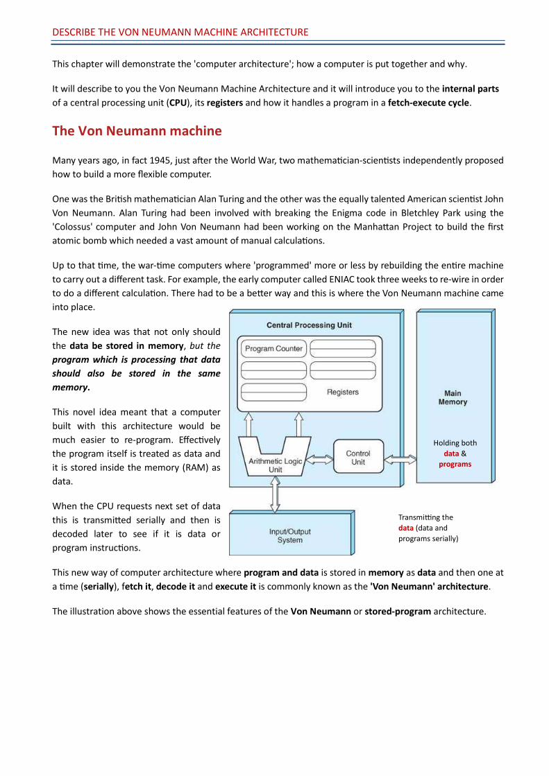
The new idea was that not only should the data be stored in memory, but the program which is processing that data should also be stored in the same memory.
This novel idea meant that a computer built with this architecture would be much easier to re-program. Effec vely the program itself is treated as data and it is stored inside the memory (RAM) as data.
When the CPU requests next set of data this is transmi ed serially and then is decoded later to see if it is data or program instruc ons.
This new way of computer architecture where program and data is stored in memory as data and then one at a me (serially), fetch it, decode it and execute it is commonly known as the 'Von Neumann' architecture.
The illustration above shows the essential features of the Von Neumann or stored-program architecture.
Holding both data &
programs
Transmi ng the data (data and programs serially)
DESCRIBE THE FEATURES OF THE VON NEUMANN ARCHITECTURE
Memory The computer will have enough memory that can hold both data and the program processing that data. In modern computers this memory is known as RAM. Control Unit The control unit will manage the process of moving data and program into and out of memory and also deals with carrying out (executing) program instructions - one at a time. This includes the idea of a 'register' to hold intermediate values. In the illustration on the previous page, the 'accumulator' is one such register.
The 'one-at-a-time' phrase means that the von Neumann architecture is a sequential processing machine.
Registers
These components are special memory locations that can be accessed very fast. Some of these registers are: Instruction Register (IR), the Program Counter (PC), and the Accumulator. Input - Output This architecture allows for the idea that a person needs to interact with the machine. Whatever values that are passed to and forth are stored once again in some internal registers which are found inside the CPU. Arithme c Logic Unit This part of the architecture is solely involved with carrying out calculations upon the data. All the usual Add, Multiply, Divide and Subtract calculations will be available but also data comparisons such as 'Greater Than', 'Less Than', 'Equal To' will be available. To summarise the ALU performs: Arithmetic calculations Logic calculations Acts as a revolving door for data going in and out of the CPU Bus Notice the arrows between components? This implies that information should flow between various parts of the computer. In a modern computer built to the Von Neumann architecture, information passes back and forth along this system 'bus'.
System Bus
A bus is a system of parallel wires connecting two or more components of a computer in order to bus signals (data) between them.
There are buses to identify locations in memory – an 'address bus' and there are also buses to allow the flow of data - a 'data bus' or
even to control the program instructions – the ‘control bus’.
https://www.youtube.com/watch?v=qgpKUAXuUQc
These three different busses we mentioned above make up what we know of the Von Neumann System. They’re also known as a system bus.
Control bus
A microprocessor uses the control bus to regulate timing of the activity and to control the components. It carries the signals that report the status of the various devices when the memory is to read from or to write on or when the i/o devices are to read or write at specific times. Various operations are performed by microprocessor with the help of this control bus. This is a dedicated bus, because all timing signals are generated according to control signal.
The control bus is a bi-directional bus, meaning that signals can be carried in both directions. The data and address busses are shared by all components of the system. Control lines must therefore be provided to ensure that access to and use of the data and address buses by the different components of the system doesn’t lead to conflict. The purpose of the control bus is to transmit command, timing and specific status information between system components. Control Bus lines include:
Bus Request: indicates that a device is requesting the use of the data bus Bus Grant: indicates that the CPU has granted access to the data bus Memory Write: causes data on the data bus to be written into the addressed location Memory Read: causes data from the addressed location to be placed on the data bus Interrupt request: indicates that a device is requesting access to the CPU Clock: used to synchronise operations Address Bus Memory is divided up internally into units called words. A word is a fixed size group of digits, typically 16, 32 or 64 bits, which is handled as a unit by the processor, and different types of processor have different word sizes. Each word in memory has its own specific address. The address bus transmits the memory addresses of words that are used as operands in program instructions, so that the data can be retrieved and sent back to the processor. When an instruction has been performed and the result is to be stored at a particular memory location, it is transmitted via the data bus. The data bus is a group of wires or lines that are used to transfer the addresses of Memory or I/O devices. It is unidirectional. If an Address bus is 16 bits this means that it can transfer maximum 16-bit address which means it can address 65,536 different memory locations. The address bus identifies particular memory locations inside the memory (RAM) or within the input / output devices. The width of the bus is identified by the number of lines; an 8bit bus will have 8 lines and these lines therefore define the maximum memory storage locations that exist. An 8-bit address buss can only service 256 memory locations although the 16-bit address bus can handle up to 64K memory locations
Data Bus
As name tells that it is used to transfer data within Microprocessor and Memory/Input or Output devices. It is bidirectional as Microprocessor requires to send or receive data. Data bus is 8 Bits long. The word length of a processor depends on data bus, that’s why Intel 8085 is called 8-bit Microprocessor because it has an 8-bit data bus. One line carries one bit and an 8 line data bus carries one byte at a time. The 16 bit database would carry two bytes at the same time.
Are there any disadvantages with the Von Neumann Architecture?
The Von Neumann architecture has been very successful with most modern computers following this architecture but there are some problems with it and because of these problems, other architectures have been developed.
Problem 1 – (See diagram on the left)
Every piece of data and instruction has to pass across the data bus in order to move from main memory into the CPU (and back again). This is a problem because the data bus is a lot slower than the rate at which the CPU can carry out instructions. This is called the 'Von Neumann bottleneck'. If nothing was done about it then the CPU would spend most of its time waiting around for instructions.
How was this eliminated?
A new special kind of memory called a 'Cache' was introduced.
Think of the data bus as a bridge that can only carry so many instructions at a time. But what if we designed a 'holding area' on the CPU side of the bridge? Then we could store the most often-used instructions in the holding area instead of having to cross the bridge every time.
This holding area is called a 'cache' (pronounced 'cash'). If the software programmer is clever enough, they will make it easier for the CPU to store the most-often used part of the code in the 'cache'. This activity is called 'code optimisation'.
To illustrate what is meant by 'often' used, consider the small piece of pseudo code (i.e. generic code) below the data bus bridge:
The instruction 'Add 1 to a variable' could be stored in the cache and would not have to be fetched from main memory for every step.
Problem 2 - Both data and programs share the same memory space. This is a problem because it is quite easy for a poorly written or faulty piece of code to write data into an area holding other instructions, so causing trashing that program.
Problem 3
Another issue is that the rate at which data needs to be fetched and the rate at which instructions need to be fetched are often very different. And yet they share the same bottlenecked data bus.
To avoid this a new architecture was introduced and this is known as The Harvard Architecture.
The idea of the Harvard Architecture is to split the memory into two parts. One part for data and another part for programs. Each part is accessed with a different bus. This means the CPU can be fetching both data and instructions at the same time. There is also less chance of program corruption.
This architecture is sometimes used within the CPU between control unit and caches (which hold data / program), but it is less used with main memory (RAM) because of complexity and cost.
Ques ons:
What is the Von – Neumann machine?
What are the disadvantages of the introduc on of the Von Neumann architecture?
How do we eliminate the Von-Neumann bo leneck? (Cache)
How do we make sure that data and program don’t overwrite one another? Good programming
Data and instruc ons need different rate of transmission. How can we eliminate this? (Harvard Architecture)
One feature of Von Neumann machine is the use of Fetch-Decode-Execute cycle. State TWO other features of Von Neumann architecture.
PURPOSE AND USE OF REGISTERS
The last page about the Von Neumann architecture made a passing reference to registers. But what are these registers?
“A register is a discrete memory location within the CPU designed to hold temporary data and/or instructions”
A modern CPU will hold a number of registers. There are a number of general purpose registers that the programmer can use to hold intermediate results whilst working through a calculation or algorithm.
Then there are special-purpose registers designed to carry out a specific role. Each of these registers are given a name so that the programmer can write their software code to access them. Different manufacturers of CPU chips call them by different names (which makes life interesting for a professional programmer!)
But generically speaking these are:
Program Counter (PC) Current Instruc on Register (CIR) Program Status Word Register (PSW) Memory Address Register (MAR)
Memory Data Register (MDR or MBR) Program Counter (PC)
This holds the address in memory of the next instruction.
For example, if the program counter has the address 305 then the next instruction will be at location 305 in main memory (RAM). When a program is running, the program counter will often just be incrementing as it addresses one instruction after the other, e.g. 305, 306, 307. However, the instructions will often modify the next address, for example, 305 becomes 39. What has happened is called a 'jump instruction'. This is how the software programmer will cause different parts of his code to run depending on some condition e.g. a conditional IF statement. It is also how an interrupt routine is serviced. The program counter will be loaded with the starting address of the interrupt routine.
Current Instruction Register (CIR)
This holds the current instruction to be executed, having been fetched from memory.
Program Status Word Register (PSW)
The PSW has a number of duties all rolled into one.
The Arithmetic Logic Unit compares two data items together, and it arranges for the result of that comparison to appear in this register i.e. the result of 'greater than' is resulted to TRUE or FALSE. The TRUE or FALSE flag will be displayed here.
The PSW also indicates if program conditions have been met that would lead to a jump to a different part of the program. In programming terms this means the result of an IF statement is TRUE or FALSE. An IF statement is important in any programming language as it allows execution to jump from one set of instructions to another.
The PSW also holds error flags that indicate a number of problems that may have happened as a result of an instruction, such as 'overflow' which means a calculation has exceeded it allowed number range.
A commonly used term is 'flag'. This denotes a single binary bit within a register. They are often used to indicate a true or false condition.
Memory Address Register (MAR)
Remember that data and program instructions have to fetch from memory? The memory address register, or MAR, holds the location in memory (address) of the next piece of data or program to be fetched (or stored).
Memory Data Register (MDR) or Memory Buffer Register
When the data or program instruction is fetched from memory, it is temporarily held in the 'Memory Data Register' or MDR for short sometimes also called the Memory Buffer Register or MBR
“A 'buffer' is a commonly used computer term to describe memory designed to hold data that is on its way to somewhere else”.
A memory buffer is a bit like the buffers on a train carriage, as the carriages connect with each other, the buffers will soak up the force. In memory, a bunch of data is absorbed quickly, then released at a controlled rate.
FETCH - DECODE - EXECUTE
When software is installed onto a personal computer (most commonly from a CD-ROM, though other media or downloading from the internet is also common), the code that makes up the program and any library files is stored on the hard drive. This code comprises of a series of instructions for performing specific tasks, and data associated with these instructions. The code remains there until the user chooses to execute the program in question, on which point sections of the code are loaded into the computer’s memory.
The CPU then executes the program from memory, processing each instruction in turn. Of course, in order to execute the instructions, it is necessary for the CPU to understand what the instruction is telling it to do. Therefore, recognition for instructions that could be encountered needs to be programmed into the processor. The instructions that can be recognized by a processor are referred to as an 'instruction set'. The instructions sets are unique for each processor.
Once the instruction has been recognised and decoded the actions are then performed before the CPU proceeds on to the next instruction in memory. This is what we call the Fetch – Decode – Execute cycle.
Before we move into the Fetch – Decode – Execute let’s have a look at the Instruction Set.
What is an Instruction Set?
Each machine instruction is composed of two parts: the op-code and the operand. The image below shows the format of an instruction for a CPU. The first three bits represent the op-code and the final six bits represent the operand. The middle bit distinguishes between operands that are memory addresses and operands that are numbers. When the bit is set to '1', the operand represents a number. If it is a ‘0’ it represents a memory address.
A simple set of machine instructions for our CPU are listed in the table below. Notice that all the op-codes are given an English mnemonic to simplify programming. Together these mnemonics are called an assembly language. Programs written in assembly language must be converted to their binary representation before the CPU can understand them. This usually done by another program called an assembler, hence the name.
Op-code Mnemonic Func on Example
001 LOAD Load the value of the operand into the Accumulator LOAD 10
010 STORE Store the value of the Accumulator at the address specified by the operand
STORE 8
011 ADD Add the value of the operand to the Accumulator ADD #5
100 SUB Subtract the value of the operand from the Accumulator
SUB #1
101 EQUAL If the value of the operand equals the value of the Accumulator, skip the next instruc on
EQUAL #20
110 JUMP Jump to a specified instruc on by se ng the Program Counter to the value of the operand
JUMP 6
111 HALT Stop execu on HALT
A simple Low Level language
In the low level language above, notice that some of the operands include a # symbol. This symbol tells the CPU that the operand represents a number rather than a memory address. Thus, when the assembler translates an instruction with a # symbol, the resulting machine code will have a '1' in the position of the number bit. Notice the central role that the Accumulator register plays. Nearly all the operations affect the value of this register since the Accumulator acts as a temporary memory location for storing calculations in progress. Let’s take a look at one of these programs
This program is called Sum. It adds the numbers stored in two memory locations and places them in another memory location:
x= 2 y = 5 z = x+y
The variables x, y, and z correspond to the memory locations 13, 14, and 15 respectively. The instructions for the program are listed below. Read through the program, and then view the
animation of this program by clicking the "View Animation" link or by typing the web address on your browser.
# Machine code Assembly code Descrip on
0 001 1 000010 LOAD #2 Load the value 2 into the Accumulator
1 010 0 001101 STORE 13 Store the value of the Accumulator in memory loca on 13
2 001 1 000101 LOAD #5 Load the value 5 into the Accumulator
3 010 0 001110 STORE 14 Store the value of the Accumulator in memory loca on 14
4 001 0 001101 LOAD 13 Load the value of memory loca on 13 into the Accumulator
5 011 0 001110 ADD 14 Add the value of memory loca on 14 to the Accumulator
6 010 0 001111 STORE 15 Store the value of the Accumulator in memory loca on 15
7 111 0 000000 HALT Stop execu on
Sum program [view animation]
http://courses.cs.vt.edu/~csonline/MachineArchitecture/Lessons/CPU/sumprogram.html
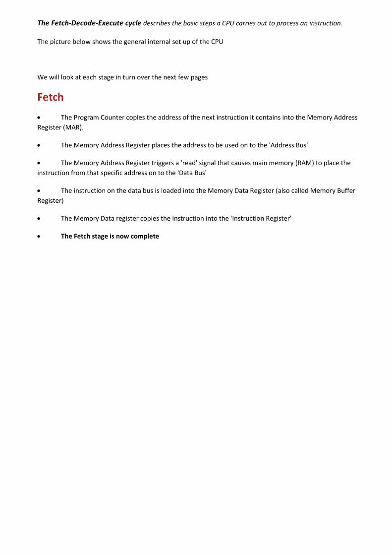
The Fetch-Decode-Execute cycle describes the basic steps a CPU carries out to process an instruction.
The picture below shows the general internal set up of the CPU
We will look at each stage in turn over the next few pages
Fetch
The Program Counter copies the address of the next instruction it contains into the Memory Address Register (MAR).
The Memory Address Register places the address to be used on to the 'Address Bus'
The Memory Address Register triggers a 'read' signal that causes main memory (RAM) to place the instruction from that specific address on to the 'Data Bus'
The instruction on the data bus is loaded into the Memory Data Register (also called Memory Buffer Register)
The Memory Data register copies the instruction into the 'Instruction Register'
The Fetch stage is now complete
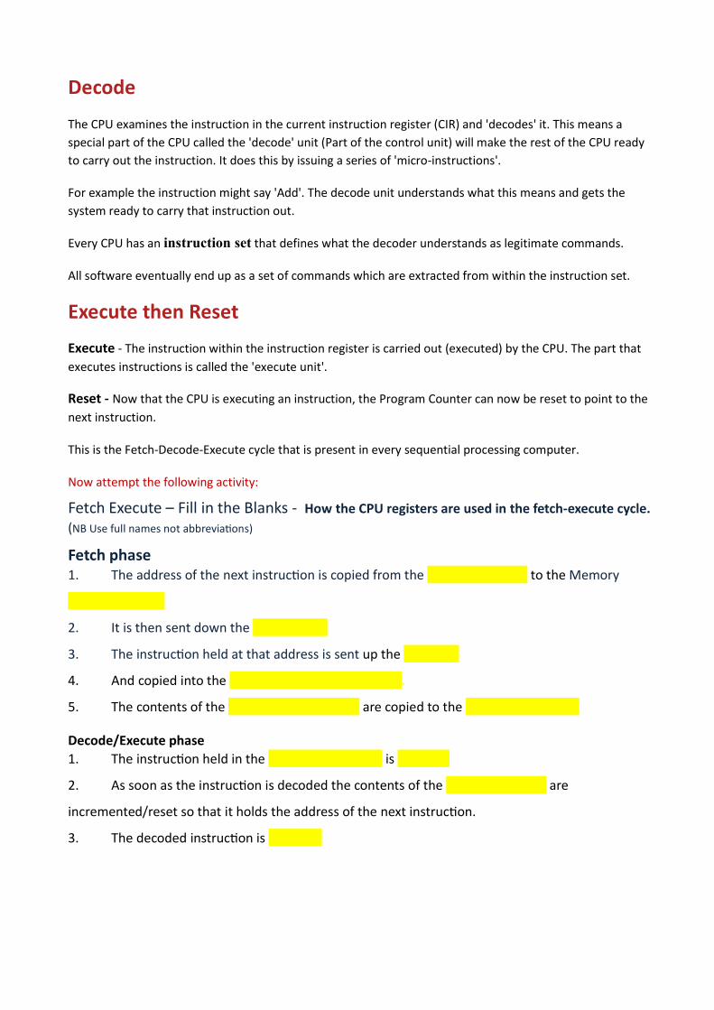
Decode
The CPU examines the instruction in the current instruction register (CIR) and 'decodes' it. This means a special part of the CPU called the 'decode' unit (Part of the control unit) will make the rest of the CPU ready to carry out the instruction. It does this by issuing a series of 'micro-instructions'. For example the instruction might say 'Add'. The decode unit understands what this means and gets the system ready to carry that instruction out.
Every CPU has an instruction set that defines what the decoder understands as legitimate commands.
All software eventually end up as a set of commands which are extracted from within the instruction set.
Execute then Reset
Execute - The instruction within the instruction register is carried out (executed) by the CPU. The part that executes instructions is called the 'execute unit'.
Reset - Now that the CPU is executing an instruction, the Program Counter can now be reset to point to the next instruction.
This is the Fetch-Decode-Execute cycle that is present in every sequential processing computer.
Now attempt the following activity:
Fetch Execute – Fill in the Blanks - How the CPU registers are used in the fetch-execute cycle. (NB Use full names not abbrevia ons)
Fetch phase 1. The address of the next instruc on is copied from the Program Counter to the Memory
Address register.
2. It is then sent down the Address Bus.
3. The instruc on held at that address is sent up the Data Bus.
4. And copied into the Memory Data/Buffer Register.
5. The contents of the Memory Data Register are copied to the Instruc on Register
Decode/Execute phase 1. The instruc on held in the Instruc on Register is Decoded
2. As soon as the instruc on is decoded the contents of the Program Counter are
incremented/reset so that it holds the address of the next instruc on.
3. The decoded instruc on is Executed
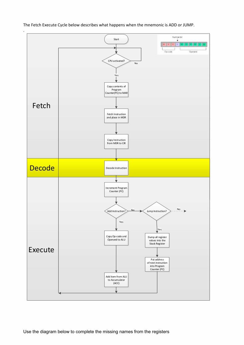
The Fetch Execute Cycle below describes what happens when the mnemonic is ADD or JUMP. .
Start
CPU activated?No
Copy contents of Program
Counter(PC) to MAR
Yes
Fetch Instruction and place in MDR
Copy Instruction from MDR to CIR
Decode Instruction
Increment Program Counter (PC)
Add Instruction?
Copy Op-code and Operand to ALU
Yes
Add item from ALU to Accumulator
(ACC)
No Jump Instruction?
Put address of next instruction
into Program Counter (PC)
Yes
Execute
Fetch
No
Decode
Dump all register values into the Stack Register
Use the diagram below to complete the missing names from the registers

Q1. Describe the Fetch – Execute Cycle.
……………………………………………………………………………………………………………………
……………………………………………………………………………………………………………………
……………………………………………………………………………………………………………………
……………………………………………………………………………………………………………………
…………………………………………………………………………………………………………………….
.………[4]
Q2. Describe how a jump instruction is executed.
……………………………………………………………………………………………………………………
……………………………………………………………………………………………………………………
……………………………………………………………………………………………………………………
……………………………………………………………………………………………………………………
……………………………………………………………………………………………………………………
……...…[2]
Q3. Iden fy/Name the component of the CPU that carries out the following tasks:
Name of Task Component (hidden)
1. Generates control/ ming signals Control 2. Carries out Logical Opera ons such as: AND, OR, NOT ALU 3. Controls decoding/execu on of instruc ons Control 4. Execu on of instruc ons ALU 5. Mathema cal opera ons (* / + - etc.) ALU 6. Small amount of very fast memory Registers
7. Holds the address of next instruc on to be executed PC
8. Decides which way data is going (IN/OUT) Control
9. Holds instruc on while it is decoded CIR 10. Holds result of ALU opera ons ACC - Accumulator 11. Example of another general purpose register Stack Pointer or Flag Register
Q4. Describe the effects of the Fetch – Decode – Execute cycle on the Program Counter (PC) and
the Memory Address Register (MAR).
……………………………………………………………………………………………………………………
……………………………………………………………………………………………………………………
……………………………………………………………………………………………………………………
……………………………………………………………………………………………………………………
……………………………………………………………………………………………………………………
……………………………………………………………………………………………………………………
……………………………………………………………………………………………………………………
……………...[5]
OTHER MACHINE ARCHITECTURES
The Von Neumann architecture is a sequential machine architecture. This has many disadvantages and one of them is that you can’t process more than one instruction at the same time. In order to make the CPU work more efficiently we introduced parallel processing.
In order to eliminate this problem, we need to look for an alternative machine architecture that can deal with more instructions at the time. There are a number of alternative parallel processing machine architectures to select from and each one has its own merits:
Pipelining
Array processors
Multiple processors
Pipelining Every CPU carries out the Fetch-Decode-Execute cycle. The idea of the pipeline is to split/break this cycle into three or more hardware processing paths within the CPU called a 'pipeline'. By dealing with the instructions in this way the processor doesn’t waste time waiting for the next execution, decoding or fetching to be carried out. This way the processing power because is carried out in parallel is more effective. If you look at the diagram below the CPU is used effectively during all stages; when pipeline 1 is doing fetching, pipeline 2 in parallel is doing the decoding and pipeline 3 in parallel again is doing the executing.
At any given time, whilst a fetch operation is taking place on pipeline 1 which occupies the data and address buses, pipeline 2 is decoding an instruction and pipeline 3 is executing an instruction. As long as the pipelines can be kept full, we are making maximum use of the CPU.
The advantages of using such an architecture:
The CPU is making efficient use of resources e.g. whilst it is dealing with the Fetch instruction the ALU is idle.
Quicker time of execution of large number of instructions
The disadvantage with this type of processing is:
It cannot handle jump or interrupts statements as the pipeline needs to be flushed(emptied) in order to deal with the interrupt instruction.
This kind of computer architecture is classified as a Single Instruction on Single Data computer or SISD.
It is very difficult to synchronise – Requires sophisticated program execution techniques e.g. organise the hardware as more than one operation is carried out at the same time
Needs to use faster technology – Faster CPU?
So in conclusion you can see that for a fixed clock speed a cpu with pipelining performs faster than CPU without pipelining.
Array or Vector Processing - Single Instruction Multiple Data (SIMD)
Some types of data can be processed independently of one another. A good example of this is the simple processing of pixels on a screen. If you wanted to make each coloured pixel a different colour according to what it currently holds. For example, "Make all Red Pixels Blue", "Make Blue Pixels Red", "Leave Green pixels alone".
A sequential processor (von Neumann type) would examine each pixel one at a time and apply the processing instruction. You can also arrange for data such as this to be an array. The simplest array looks like this:
{element 1, element 2, ...} this is called a '1 dimensional array' or a 'vector'
A slightly more complicated array would have rows and columns:
{element 1, element 2
element 3, element 4}
This is called a '2 dimensional' array or 'matrix'. The matrix is fundamental to graphics work.
An array processor (or vector processor) carries out a single instruction but on multiple data; one processor but with a number of Arithmetic Logic Units (ALU) that allows all the elements of an array of data to be processed at the same time. The illustration on the right shows the architecture of an array or vector processor
With an array processor, a single instruction is issued by a control unit and that a single instruction is applied to a number of data storage location sets at the same time. Like this the processor is executing the one instruction on four different locations at the same time and therefore will execute the instruction much quicker than a sequential processor.
An array processor is a Single Instruction on Multiple Data computer or SIMD. You will find games consoles and graphics cards making heavy use of array processors to shift those pixels about. This type of processor is ideal for weather forecasting/airflow simulation on a new aircraft etc.
Limitations of Array Processing
This architecture relies on the fact that the data sets are all acting on a single instruction. However, if these data sets somehow rely on each other then you cannot apply parallel processing. For example, if data A has to be processed before data B then you cannot do A and B simultaneously. This dependency is what makes parallel processing difficult to implement. This is why sequential machines are still extremely useful.
Let’s consider an example of a simple multiplication of a series of numbers 1, 9, 2 and 8, all of which need to be multiplied by the number 3. An ordinary CPU without array processing will need to load the 4 numbers one at a time (4 Loads), multiply each one by 3 (4 times) and save the result of each multiplication (4 times). There will be 12 instructions altogether to be carried out. Using an array processor, we cut down the number of instructions quite considerably as one instruction of load, multiply and save is applied at the same time to 4 different registers.
Q1. Describe the term array processor.
…………………………………………………………………………………………………………………………………………………………………………
…………………………………………………………………………………………………………………………………………………………………………
…………………………………………………………………………………………………………………………………………………………………………
…………………………………………………………………………………………………………………………………………………………………………
………………………………………………………………..…….…[2]
Q2. Give an example of the type of task for which an array processor is most suitable.
…………………………………………………………………………………………………………………………………………………………………………
…………………………………………………………………………………………………………………………………………………………………………
…………………………………………………………………………………………………………………………………………………………………………
…………………………………………………………………………………………………………………………………………………………………………
………………………………………………………………..…….…[2]
Multiple Processors
Moving on from an array processor, where a single instruction acts upon multiple data sets and the next level of parallel processing is to have multiple processors that carry out many instructions by acting upon multiple data sets.
This is achieved by having a number of CPUs being applied to a single problem, with each CPU carrying out only part of the overall problem.
A good example of this architecture is a supercomputer. For example the massively parallel IBM Blue Gene supercomputer that has 4,098 processors, allowing for 560 TeraFlops of processing. This is applied to problems such as predicting climate change or running new drug simulations. It is an ideal architecture to use for large problems that can be broken down into smaller sub-problems.
We have something similar but in a smaller scale at home. Our home computers now have multiple cores. For example the Intel Core Duo has two CPUs (called 'cores') inside the chip, whilst the Quad core has four. A multi-core computer is a 'Multiple Instruction Multiple Data' computer or MIMD
Limita ons of mul -core processing
This architecture is dependent on being able to cut a problem down into chunks, each chunk can then be processed independently. But not many problems can be broken down in this way and so it remains a less used architecture.
Furthermore, the software programmer has to write the code to take advantage of the multi-core CPUs. This is actually quite difficult and even now most applications running on a multi-core CPU such as the Intel 2 Duo will not be making use of both cores most of the time.
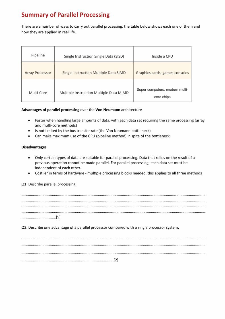
Summary of Parallel Processing
There are a number of ways to carry out parallel processing, the table below shows each one of them and how they are applied in real life.
Pipeline Single Instruc on Single Data (SISD) Inside a CPU
Array Processor Single Instruc on Mul ple Data SIMD Graphics cards, games consoles
Mul -Core Mul ple Instruc on Mul ple Data MIMD Super computers, modern multi-
core chips
Advantages of parallel processing over the Von Neumann architecture
Faster when handling large amounts of data, with each data set requiring the same processing (array and mul -core methods)
Is not limited by the bus transfer rate (the Von Neumann bo leneck) Can make maximum use of the CPU (pipeline method) in spite of the bo leneck
Disadvantages
Only certain types of data are suitable for parallel processing. Data that relies on the result of a previous opera on cannot be made parallel. For parallel processing, each data set must be independent of each other.
Costlier in terms of hardware - mul ple processing blocks needed, this applies to all three methods
Q1. Describe parallel processing.
…………………………………………………………………………………………………………………………………………………………………………………………………………………………………………………………………………………………………………………………………………………………………………………………………………………………………………………………………………………………………………………………………………………………………………………………………………..…….………………………………………………………………………………………………………………………[5]
Q2. Describe one advantage of a parallel processor compared with a single processor system.
…………………………………………………………………………………………………………………………………………………………………………
…………………………………………………………………………………………………………………………………………………………………………
…………………………………………………………………………………………………………………………………………………………………………
…………………………………………………………………………..…….…[2]
Co-processor (Maths co-processor) So far, we have discussed parallel processing as a means of speeding up data processing. This is fine but it does make an assumption that the Arithmetic Logic Unit (ALU) within the CPU is perfect for handling all kinds of data but this is not always true.
There are two basic ways of doing calculations within a CPU:
a) Integer maths which only deals with whole numbers or
b) floating point maths which can deal with decimal / fractional numbers.
Handling floating point numbers efficiently requires wide registers to deal with a calculation in one go but the CPU architect may not want to dedicate precious hardware space in his CPU for these wider registers.
So the idea of a 'Maths co-processor' came about. A co-processor is especially designed to carry out floating point calculation extremely quickly. It co-exists with the CPU on the motherboard. Whenever a floating point calculation needs to be done, the CPU hands the task over to the co-processor then carries on with doing something else until the task is complete.
The advantage of having a co-processor is that calculation (and hence performance) is much faster.
The disadvantage is that it is more expensive, requires more motherboard space and takes more power. On top of this Co-processors often require tasks to be handed to them by the central processor.
But if the computer is dedicated to handling heavy floating point work then it may be worth it. For instance a computer within a signal processing card in a communication system may include a maths co-processor to process the incoming data as quickly as possible.
Operations performed by the coprocessor may be floating point arithmetic, graphics, signal processing, string processing, and encryption. By offloading processor-intensive tasks from the main processor, coprocessors can accelerate the system performance. Many computer manufactures allow their customers to customise their computers by opting to have a coprocessor or not so that those who do not need the extra performance don't need to pay for it.
Q1. In some computer systems a co-processor may be used. Explain the term co-processor.
…………………………………………………………………………………………………………………………………………………………………………
…………………………………………………………………………………………………………………………………………………………………………
…………………………………………………………………………………………………………………………………………………………………………
…………………………………………………………………………..…….…[3]
Q3. Explain with an aid of an example, the following statement: ‘A co-processor is a simple form of parallel processor’
.…………………………………………………………………………………………………………………………………………………………………………………………………………………………………………………………………………………………………………………………………………………………………………………………………………………………………………………………………………………………………………………………………………………………………………………………………………………………………………………………………………………………………………………………………………………………………………………………………………………………………………………………..…….…[2]
Q4. Discuss the use of different computer architectures for different problem solutions. (the quality of your written communication will be assessed in your answer to this question)
…………………………………………………………………………………………………………………………………………………………………………………………………………………………………………………………………………………………………………………………………………………………………………………………………………………………………………………………………………………………………………………………………………………………………………………………………………………………………………………………………………………………………………

………………………………………………………………………………………………………………………………………………………………………………………………………………………………………………………………………………………………………………………………………………………………………………………………………………………………………………………………………………………………………………………………………………………………………………………………………………………………………………………………………………………………………………………………………………………………………………………………………………………………………………………………………………………………………………………………………………………………………………………………………………………………………………………………………………………………………………………………………………………………………………………………………………………………………………………………………………………………………………………………………………………………………………………………………………………………………………………………………………………………………………………………………………………………………………………………………………………………………………………………………………………………………………………………………………………………………………………………………………………………………………………………………………………………………………………………………………………………………………………………………………………………………………………………………………………………………………………………………………………………………………………………………………………………………………………………………………………………………………………………………………………………………………………………………………………………………………………………………………………………………………………………………………………………………………………………………………………………………………………………………………………………………………………………………………………………………………………………………………………………………………………………………………………………………………………………………………………………………………………………………………………………………………………………………………………………………………………………………………………………………………………………………………………………………………………………………………………………………………………………………………………………………………………………………………………………………………………………………………………………………………………………………………………………………………………………………………………………………………………………………………………………………………………………………………………………………………………………………………………………………………………………………………………………………………………………………………………………………………………………………………………………………………………………………………………………………………………………………………………………………………………………………………………………………………………………………………………………………………………………………………………………………………………………..…….…[8]
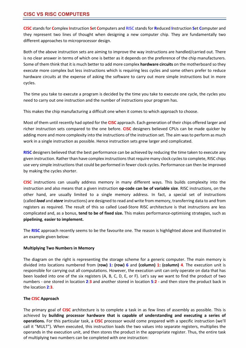
CISC VS RISC COMPUTERS
CISC stands for Complex Instruction Set Computers and RISC stands for Reduced Instruction Set Computer and they represent two lines of thought when designing a new computer chip. They are fundamentally two different approaches to microprocessor design.
Both of the above instruction sets are aiming to improve the way instructions are handled/carried out. There is no clear answer in terms of which one is better as it depends on the preference of the chip manufacturers. Some of them think that it is much better to add more complex hardware circuits on the motherboard so they execute more complex but less instructions which is requiring less cycles and some others prefer to reduce hardware circuits at the expense of asking the software to carry out more simple instructions but in more cycles.
The time you take to execute a program is decided by the time you take to execute one cycle, the cycles you need to carry out one instruction and the number of instructions your program has.
This makes the chip manufacturing a difficult one when it comes to which approach to choose.
Most of them until recently had opted for the CISC approach. Each generation of their chips offered larger and richer instruction sets compared to the one before. CISC designers believed CPUs can be made quicker by adding more and more complexity into the instructions of the instruction set. The aim was to perform as much work in a single instruction as possible. Hence instruction sets grew larger and complicated.
RISC designers believed that the best performance can be achieved by reducing the time taken to execute any given instruction. Rather than have complex instructions that require many clock cycles to complete, RISC chips use very simple instructions that could be performed in fewer clock cycles. Performance can then be improved by making the cycles shorter.
CISC instructions can usually address memory in many different ways. This builds complexity into the instruction and also means that a given instruction op-code can be of variable size. RISC instructions, on the other hand, are usually limited to a single memory address. In fact, a special set of instructions (called load and store instructions) are designed to read and write from memory, transferring data to and from registers as required. The result of this so called Load-Store RISC architecture is that instructions are less complicated and, as a bonus, tend to be of fixed size. This makes performance-optimising strategies, such as pipelining, easier to implement.
The RISC approach recently seems to be the favourite one. The reason is highlighted above and illustrated in an example given below:
Multiplying Two Numbers in Memory
The diagram on the right is representing the storage scheme for a generic computer. The main memory is divided into locations numbered from (row) 1: (row) 6 and (column) 1: (column) 4. The execution unit is responsible for carrying out all computations. However, the execution unit can only operate on data that has been loaded into one of the six registers (A, B, C, D, E, or F). Let's say we want to find the product of two numbers - one stored in location 2:3 and another stored in location 5:2 - and then store the product back in the location 2:3.
The CISC Approach
The primary goal of CISC architecture is to complete a task in as few lines of assembly as possible. This is achieved by building processor hardware that is capable of understanding and executing a series of operations. For this particular task, a CISC processor would come prepared with a specific instruction (we'll call it "MULT"). When executed, this instruction loads the two values into separate registers, multiplies the operands in the execution unit, and then stores the product in the appropriate register. Thus, the entire task of multiplying two numbers can be completed with one instruction:

MULT 2:3, 5:2
MULT is what is known as a "complex instruction." It operates directly on the computer's memory banks and does not require the programmer to explicitly call any loading or storing functions thus requires less registers. It closely resembles a command in a higher level language. For instance, if we let "a" represent the value of 2:3 and "b" represent the value of 5:2, then this command is identical to the C statement "a = a * b."
One of the primary advantages of this system is that the compiler has to do very little work to translate a high-level language statement into assembly. Because the length of the code is relatively short, very little RAM is required to store instructions. The emphasis is put on building complex instructions directly into the hardware.
The RISC Approach
RISC processors only use simple instructions that can be executed within one clock cycle. Thus, the "MULT" command described above could be divided into three separate commands: "LOAD," which moves data from the memory bank to a register, "PROD," which finds the product of two operands located within the registers, and "STORE," which moves data from a register to the memory banks. In order to perform the exact series of steps described in the CISC approach, a programmer would need to code four lines of assembly:
LOAD A, 2:3 LOAD B, 5:2 PROD A, B STORE 2:3, A
At first, this may seem like a much less efficient way of completing the operation. Because there are more lines of code, more RAM is needed to store the assembly level instructions. The compiler must also perform more work to convert a high-level language statement into code of this form.
However, the RISC strategy also brings some very important advantages. Because each instruction requires only one clock cycle to execute, the entire program will execute in approximately the same amount of time as the multi-cycle "MULT" command. These RISC "reduced instructions" require less transistors of hardware space than the complex instructions, leaving more room for general purpose registers. Because all of the instructions execute in a uniform amount of time (i.e. one clock), pipelining is possible.
Separating the "LOAD" and "STORE" instructions actually reduces the amount of work that the computer must perform. After a CISC-style "MULT" command is executed, the processor automatically erases the registers. If one of the operands needs to be used for another computation, the processor must re-load the data from the memory bank into a register. In RISC, the operand will remain in the register until another value is loaded in its place.
The Performance Equation The following equation is commonly used for expressing a computer's performance ability:
The CISC approach attempts to minimize the number of instructions per program, sacrificing the number of cycles per instruction. RISC does the opposite, reducing the cycles per instruction at the cost of the number of instructions per program.
RISC Roadblocks
Despite the advantages of RISC based processing, RISC chips took over a decade to gain a foothold in the commercial world. This was largely due to a lack of software support. It was because of this companies were reluctant to invest on the RISC based processing.
Although Apple's Power Macintosh line featured RISC-based chips and Windows NT was RISC compatible, Windows 95 and Windows 98 were designed with CISC processors in mind. Many companies were unwilling to take a chance with the emerging RISC technology. Without commercial interest, processor developers were unable to manufacture RISC chips in large enough volumes to make their price competitive.
The Overall RISC Advantage
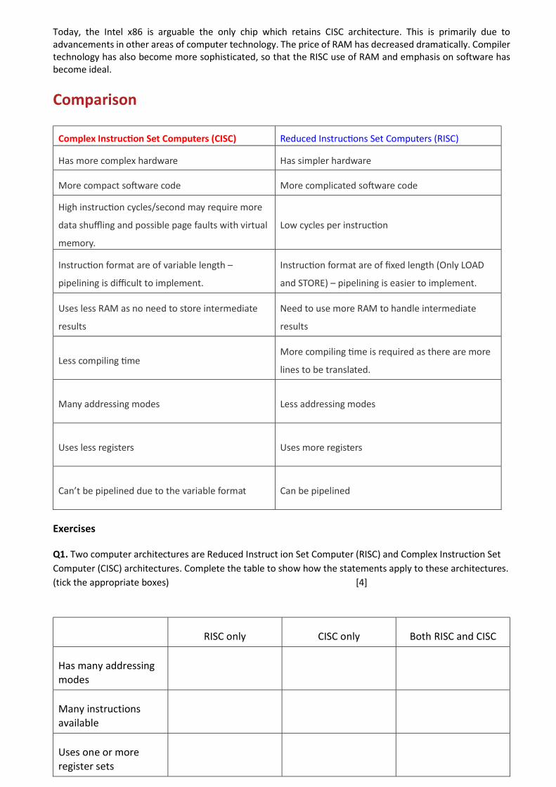
Today, the Intel x86 is arguable the only chip which retains CISC architecture. This is primarily due to advancements in other areas of computer technology. The price of RAM has decreased dramatically. Compiler technology has also become more sophisticated, so that the RISC use of RAM and emphasis on software has become ideal.
Comparison
Complex Instruc on Set Computers (CISC) Reduced Instruc ons Set Computers (RISC)
Has more complex hardware Has simpler hardware
More compact so ware code More complicated so ware code
High instruc on cycles/second may require more
data shuffling and possible page faults with virtual
memory.
Low cycles per instruc on
Instruc on format are of variable length –
pipelining is difficult to implement.
Instruc on format are of fixed length (Only LOAD
and STORE) – pipelining is easier to implement.
Uses less RAM as no need to store intermediate
results
Need to use more RAM to handle intermediate
results
Less compiling me More compiling me is required as there are more
lines to be translated.
Many addressing modes Less addressing modes
Uses less registers Uses more registers
Can’t be pipelined due to the variable format Can be pipelined
Exercises
Q1. Two computer architectures are Reduced Instruct ion Set Computer (RISC) and Complex Instruction Set Computer (CISC) architectures. Complete the table to show how the statements apply to these architectures. (tick the appropriate boxes) [4]
RISC only CISC only Both RISC and CISC
Has many addressing modes
Many instructions available
Uses one or more register sets
Uses only simple instructions
Q2. Compare the number of machine cycles used by RISC and CISC to complete a single task.
…………………………………………………………………………………………………………………………………………………………………………
…………………………………………………………………………………………………………………………………………………………………………
…………………………………………………………………………………………………………………………………………………………………………
…………………………………………………………………………………………………………………………………………………………………………
………………………………………………………………..…….…[2]
Q3. State three features of a Complex Instruction Set Computer (CISC) architecture.
…………………………………………………………………………………………………………………………………………………………………………
…………………………………………………………………………………………………………………………………………………………………………
…………………………………………………………………………………………………………………………………………………………………………
…………………………………………………………………………………………………………………………………………………………………………
………………………………………………………………..…….…[3]
Q4. Explain one advantage and one disadvantage, other than cost, of a CISC architecture compared with a Reduced Instruction Set Computer (RISC) architecture.
…………………………………………………………………………………………………………………………………………………………………………
…………………………………………………………………………………………………………………………………………………………………………
…………………………………………………………………………………………………………………………………………………………………………
…………………………………………………………………………………………………………………………………………………………………………
………………………………………………………………..…….…[2]