solid-state reactions between ni and sn–ag–cu solders with different cu concentrations
TRANSCRIPT

Materials Science and Engineering A 396 (2005) 385–391
Solid-state reactions between Ni and Sn–Ag–Cu solderswith different Cu concentrations
W.C. Luoa, C.E. Hoa, J.Y. Tsaia, Y.L. Lin a, C.R. Kaoa,b,∗a Department of Chemical and Materials Engineering, National Central University, Jhongli City, Taiwan
b Institute of Materials Science and Engineering, National Central University, Jhongli City, Taiwan
Received 17 August 2004; received in revised form 28 January 2005; accepted 3 February 2005
Abstract
It had been reported that, during the reflow of the Sn–Ag–Cu solders over the Ni-bearing surface finishes, a slight variation in Cu con-centration produced different reaction products at the interface. In this study, we extended our earlier efforts to investigate whether thisstrong Cu concentration dependency also existed for the solid-state aging reaction between the Sn–Ag–Cu solders and Ni. Specifically, fiveSn–3.9Ag–xCu solders (x= 0.2, 0.4, 0.5, 0.6, and 0.8) were reacted with Ni at 180◦C. It was found that the strong Cu concentration dependencyd d, the samei wedt chanismsf©
K
1
vicretqtbSisttj
thesol-tions be-
rion in
-.%, ais-e.ount
iestheflow,
te.
0d
isappeared after the solid-state aging at high temperatures for sufficient periods of time. For all the Cu concentrations studientermetallic compounds, a layer of (Cu1− yNiy)6Sn5 and a layer of (Ni1− xCux)3Sn4, formed at the interface after aging. This study shohat the initial difference in the intermetallic compounds right after reflow could be aged out at high temperatures. The growth meor (Cu1− yNiy)6Sn5 and (Ni1− xCux)3Sn4 were different, and were pointed out in this study.
2005 Elsevier B.V. All rights reserved.
eywords:Sn–Ag–Cu; Interfacial reaction; Surface finish; Lead-free solder
. Introduction
The Pb–Sn solder is an easily accessible material withery good mechanical properties. Unfortunately, the Pb tox-city has led to the banning of Pb in solders. Two re-ent European Union directives, RoHS (Directive on theestriction of the use of certain hazardous substances inlectrical and electronic equipment) and WEEE (Direc-
ive on Waste Electrical and Electronic Equipment), re-uire new electrical and electronic equipments produced af-
er July 1, 2006 to be lead-free. Several review papers hadeen published on the status of Pb-free solders[1–4]. Then–Ag–Cu solder family is regarded as one the most promis-
ng lead-free replacements for the Pb–Sn. The Sn–Ag–Cuolder family has compositions (wt.%) near the Sn–Ag–Cuernary eutectic at Sn–(3.5± 0.3)Ag–(0.9± 0.2)Cu[5], andhe Sn–3.9Ag–0.6Cu solder has been recommended by a ma-or industrial consortium[6].
∗ Corresponding author. Tel.: +886 342 27382; fax: +886 342 27382.E-mail address:[email protected] (C.R. Kao).
Nickel is a very common metal surface finish used inelectronic packages. The function of Ni is to serve as aderable diffusion barrier layer to prevent the rapid reacbetween the solder and the Cu layer below. The reactiontween Ni and solders had been studied before[7–26]. It hadbeen reported that the reaction of Ni withliquidSn–Ag–Cu oSn–Cu solders were very sensitive to the Cu concentratthe solders[12–15]. At low Cu concentrations (≤0.2 wt.%),only a continuous (Ni1− xCux)3Sn4 layer formed at the interface. When the Cu concentration increased to 0.4 wtcontinuous (Ni1− xCux)3Sn4 layer and a small amount of dcontinuous (Cu1− yNiy)6Sn5 particles formed at the interfacWhen the Cu concentration increased to 0.5 wt.%, the amof (Cu1− yNiy)6Sn5 increased and (Cu1− yNiy)6Sn5 becamea continuous layer. Beneath this (Cu1− yNiy)6Sn5 layer was avery thin but continuous layer of (Ni1− xCux)3Sn4. At higherCu concentrations (0.6–3.0 wt.%), (Ni1− xCux)3Sn4 disap-peared, and only (Cu1− yNiy)6Sn5 was present. These studshow that a precise control over the Cu concentration insolders is needed to produce consistent results during rewhich is a reaction betweenliquid solders and solid substra
921-5093/$ – see front matter © 2005 Elsevier B.V. All rights reserved.oi:10.1016/j.msea.2005.02.008
386 W.C. Luo et al. / Materials Science and Engineering A 396 (2005) 385–391
This is because the types of intermetallic at the solder/Ni in-terface had been shown to have a clear effect on the fracturestrength and reliability of a device[27].
The objective of this study is to investigate whether thisstrong Cu concentration dependency also exists for the reac-tion between Ni andsolidSn–Ag–Cu solders. In other words,we would like to know whether this dependency still existduring the aging of the solder joints.
2. Experimental
Five different Sn–Ag–Cu solders (Sn–3.9–Ag–0.2Cu,Sn–3.9Ag–0.4Cu, Sn–3.9Ag–0.5Cu, Sn–3.9Ag–0.6Cu, andSn–3.9Ag–0.8Cu) were prepared from 99.99% purity ele-ments. A balance with a 0.0001 g precision was used to weighthe elements, producing a maximum composition error of0.01 wt.%. Mixtures of the pure elements with the chosencomposition were sealed in quartz capsules evacuated to avacuum of 15 mm Hg, and then melted at 850◦C for 250 h toproduce the solder ingots with different Cu concentrations.For every reaction, a small piece of solder (200± 10 mg) wascut from an ingot. The concentrations of Ag and Cu in suchsolder pieces were checked by ICP (induction couple plasma)spectrum analysis to ensure the composition is the same ast ,9 ces.B hedo ast with
acetone, etched in a 50 vol.% HCl solution (in methanol) for30 s, and coated with a mildly active rosin flux. Each solderpiece was placed on a Ni disk and then reflowed through a re-flow oven. The peak reflow temperature was fixed at 250◦C,and heating rate and cooling rate were both fixed at 1◦C/s,respectively. The time the solder was in the molten state was120 s. After reflow, the samples were aged at 180◦C for aslong as 5000 h.
After aging, the samples were mounted in epoxy, sectionedby using a low-speed diamond saw, and metallurgically pol-ished in preparation for characterization. The reaction zonefor each sample was examined using an optical microscopeand a scanning electron microscope (SEM). The composi-tions of the reaction products were determined using an elec-tron microprobe, operated at 20 keV. In microprobe analysis,the concentration of each element was measured indepen-dently, and the total weight percentage of all elements waswithin 100± 1% in each case. For every data point, at leastfour measurements were made and the average value wasreported.
3. Results
The interfaces between Ni and Sn–Ag–Cu solders righta efs.[ nly( on-c inu-o us
he ingot. Nickel disks (6.35 mm diameter× 0.50 mm thick9.995% pure) were utilized to react with the solder pieefore reaction, each Ni disk was metallurgically polisn both surfaces. The 1�m diamond abrasive was used
he last polishing step. The Ni disks were then cleaned
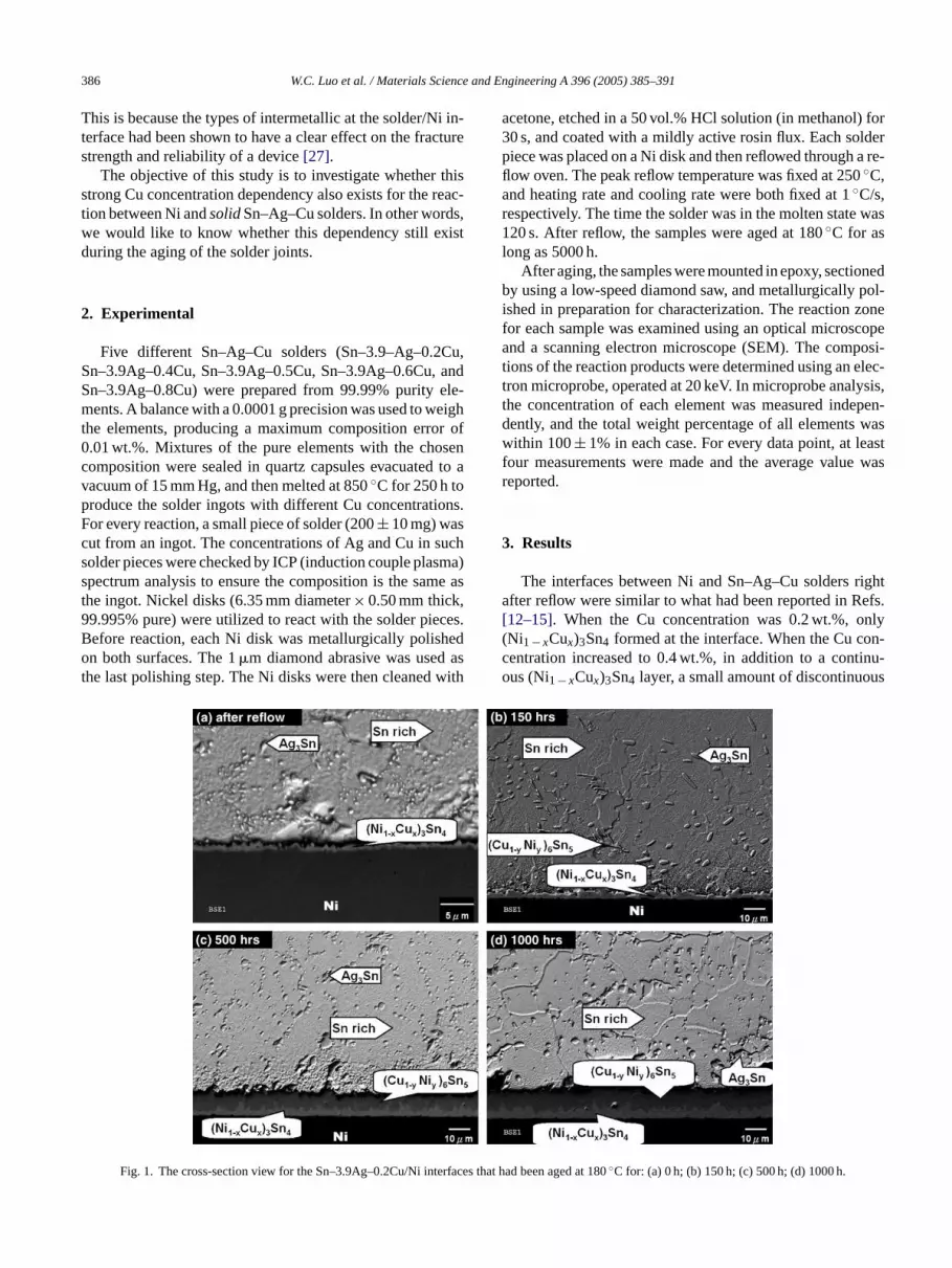
Fig. 1. The cross-section view for the Sn–3.9Ag–0.2Cu/Ni interfaces
fter reflow were similar to what had been reported in R12–15]. When the Cu concentration was 0.2 wt.%, oNi1− xCux)3Sn4 formed at the interface. When the Cu centration increased to 0.4 wt.%, in addition to a contus (Ni1− xCux)3Sn4 layer, a small amount of discontinuo
that had been aged at 180◦C for: (a) 0 h; (b) 150 h; (c) 500 h; (d) 1000 h.
W.C. Luo et al. / Materials Science and Engineering A 396 (2005) 385–391 387
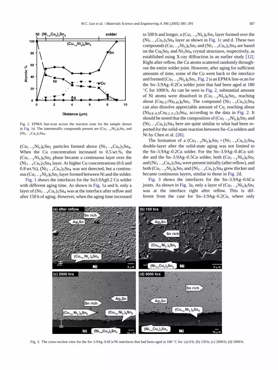
Fig. 2. EPMA line-scan across the reaction zone for the sample shownin Fig. 1d. The intermetallic compounds present are (Cu1− yNiy)6Sn5 and(Ni1− xCux)3Sn4.
(Cu1− yNiy)6Sn5 particles formed above (Ni1− xCux)3Sn4.When the Cu concentration increased to 0.5 wt.%, the(Cu1− yNiy)6Sn5 phase became a continuous layer over the(Ni1− xCux)3Sn4 layer. At higher Cu concentrations (0.6 and0.8 wt.%), (Ni1− xCux)3Sn4 was not detected, but a continu-ous (Cu1− yNiy)6Sn5 layer formed between Ni and the solder.
Fig. 1shows the interfaces for the Sn3.9Ag0.2 Cu solderwith different aging time. As shown inFig. 1a and b, only alayer of (Ni1− xCux)3Sn4 was at the interface after reflow andafter 150 h of aging. However, when the aging time increased
to 500 h and longer, a (Cu1− yNiy)6Sn5 layer formed over the(Ni1− xCux)3Sn4 layer as shown inFig. 1c and d. These twocompounds (Cu1− yNiy)6Sn5 and (Ni1− xCux)3Sn4 are basedon the Cu6Sn5 and Ni3Sn4 crystal structures, respectively, asestablished using X-ray diffraction in an earlier study[12].Right after reflow, the Cu atoms scattered randomly through-out the entire solder joint. However, after aging for sufficientamounts of time, some of the Cu went back to the interfaceand formed (Cu1− yNiy)6Sn5.Fig. 2is an EPMA line-scan forthe Sn–3.9Ag–0.2Cu solder joint that had been aged at 180◦C for 1000 h. As can be seen inFig. 2, substantial amountof Ni atoms were dissolved in (Cu1− yNiy)6Sn5, reachingabout (Cu0.57Ni0.43)6Sn5. The compound (Ni1− xCux)3Sn4can also dissolve appreciable amount of Cu, reaching about(Ni0.8–0.9Cu0.2–0.1)3Sn4, according to the data inFig. 2. Itshould be noted that the composition of (Cu1− yNiy)6Sn5 and(Ni1− xCux)3Sn4 here are quite similar to what had been re-ported for the solid-state reaction between Sn–Cu solders andNi by Chen et al.[26].
The formation of a (Cu1− yNiy)6Sn5 + (Ni1− xCux)3Sn4double-layer after the solid-state aging was not limited tothe Sn–3.9Ag–0.2Cu solder. For the Sn–3.9Ag–0.4Cu sol-der and the Sn–3.9Ag–0.5Cu solder, both (Cu1− yNiy)6Sn5and (Ni1− xCux)3Sn4 were present initially (after reflow), andboth (Cu1− yNiy)6Sn5 and (Ni1− xCux)3Sn4 grew thicker andb
Cujw if-f only
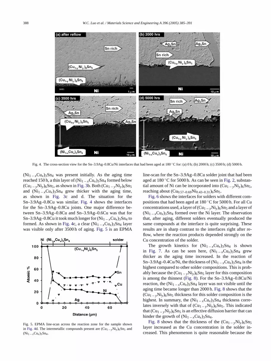
rfaces that had been aged at 180◦C for: (a) 0 h; (b) 150 h; (c) 2000 h; (d) 5000 h.
Fig. 3. The cross-section view for the Sn–3.9Ag–0.6Cu/Ni inteecame continuous layers, similar to those inFig. 2d.Fig. 3 shows the interfaces for the Sn–3.9Ag–0.6
oints. As shown inFig. 3a, only a layer of (Cu1− yNiy)6Sn5as at the interface right after reflow. This is d
erent from the case for Sn–3.9Ag–0.2Cu, where
388 W.C. Luo et al. / Materials Science and Engineering A 396 (2005) 385–391
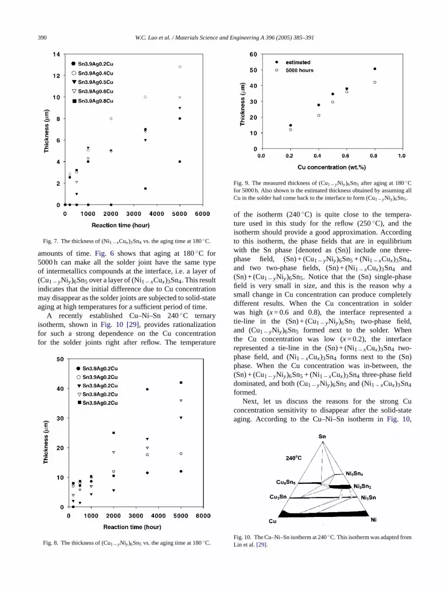
Fig. 4. The cross-section view for the Sn–3.9Ag–0.8Cu/Ni interfaces that had been aged at 180◦C for: (a) 0 h; (b) 2000 h; (c) 3500 h; (d) 5000 h.
(Ni1− xCux)3Sn4 was present initially. As the aging timereached 150 h, a thin layer of (Ni1− xCux)3Sn4 formed below(Cu1− yNiy)6Sn5, as shown inFig. 3b. Both (Cu1− yNiy)6Sn5and (Ni1− xCux)3Sn4 grew thicker with the aging time,as shown in Fig. 3c and d. The situation for theSn–3.9Ag–0.8Cu was similar.Fig. 4 shows the interfacesfor the Sn–3.9Ag–0.8Cu joints. One major difference be-tween Sn–3.9Ag–0.8Cu and Sn–3.9Ag–0.6Cu was that forSn–3.9Ag–0.8Cu it took much longer for (Ni1− xCux)3Sn4 toformed. As shown inFig. 4c, a clear (Ni1− xCux)3Sn4 layerwas visible only after 3500 h of aging.Fig. 5 is an EPMA
F howni(
line-scan for the Sn–3.9Ag–0.8Cu solder joint that had beenaged at 180◦C for 5000 h. As can be seen inFig. 2, substan-tial amount of Ni can be incorporated into (Cu1− yNiy)6Sn5,reaching about (Cu0.57–0.69Ni0.43–0.31)6Sn5.
Fig. 6shows the interfaces for solders with different com-positions that had been aged at 180◦C for 5000 h. For all Cuconcentrations used, a layer of (Cu1− yNiy)6Sn5 and a layer of(Ni1− xCux)3Sn4 formed over the Ni layer. The observationthat, after aging, different solders eventually produced thesame compounds at the interface is quite surprising. Theseresults are in sharp contrast to the interfaces right after re-flow, where the reaction products depended strongly on theCu concentration of the solder.
The growth kinetics for (Ni1− xCux)3Sn4 is shownin Fig. 7. As can be seen here, (Ni1− xCux)3Sn4 grewthicker as the aging time increased. In the reaction ofSn–3.9Ag–0.4Cu/Ni, the thickness of (Ni1− xCux)3Sn4 is thehighest compared to other solder compositions. This is prob-ably because the (Cu1− yNiy)6Sn5 layer for this compositionis among the thinnest (Fig. 8). For the Sn–3.9Ag–0.8Cu/Nireaction, the (Ni1− xCux)3Sn4 layer was not visible until theaging time became longer than 2000 h.Fig. 8shows that the(Cu1− yNiy)6Sn5 thickness for this solder composition is thehighest. In summary, the (Ni1− xCux)3Sn4 thickness corre-lates inversely with that of (Cu1− yNiy)6Sn5. This indicatedt anh
l r in-c se the
ig. 5. EPMA line-scan across the reaction zone for the sample sn Fig. 4d. The intermetallic compounds present are (Cu1− yNiy)6Sn5 andNi1− xCux)3Sn4.
hat (Cu1− yNiy)6Sn5 is an effective diffusion barrier that cinder the growth of (Ni1− xCux)3Sn4.
Fig. 8 shows that the thickness of the (Cu1− yNiy)6Sn5ayer increased as the Cu concentration in the soldereased. This phenomenon is quite reasonable becau

W.C. Luo et al. / Materials Science and Engineering A 396 (2005) 385–391 389
Fig. 6. The cross-section view for the solders/Ni interfaces that had aged at 180◦C for 5000 h for: (a) Sn–3.9Ag–0.2Cu/Ni interface; (b) Sn–3.9Ag–0.4Cu/Niinterface; (c) Sn–3.9Ag–0.5Cu/Ni interface; (d) Sn–3.9Ag–0.6Cu/Ni interface; (e) Sn–3.9Ag–0.8Cu/Ni interface. For all the solder compositions, both(Ni1− xCux)3Sn4 and (Cu1− yNiy)6Sn5 formed.
amount of Cu available increased with the Cu concentration inthe solder. It is interesting to estimate how much Cu in the sol-der had gone back to the interface to become (Cu1− yNiy)6Sn5after 5000 h of aging. Alternatively, we can ask how thickwould (Cu1− yNiy)6Sn5 had been if all Cu had gone back tothe interface to form (Cu1− yNiy)6Sn5. Fig. 9 is a compari-son between the measured thickness of (Cu1− yNiy)6Sn5 after5000 h of aging and the estimated thickness by assuming allCu had formed (Cu1− yNiy)6Sn5 at the interface. In calculat-ing the estimated thickness, the density of (Cu1− yNiy)6Sn5was taken to be the same as that of Cu6Sn5, which was re-ported to be 8.28 g/cm3 [28]. The solder used in each samplewas 200 mg, and the wetting area (the area that the solder wasin direct contact with the Ni substrate) of each sample was0.16 cm2. The values for the composition of (Cu1− yNiy)6Sn5were from the EPMA measurements. It can be seen from
Fig. 9that the measured thickness was always slightly smallerthan that of the estimated thickness. In other words, after5000 h of aging, most, but not all, of the Cu atoms had goneback to the interface.
4. Discussion
According to earlier studies[12–15], the reac-tion product right after reflow was very sensitive tothe Cu composition in the solder. With increasingCu concentration, the reaction product switched from(Ni1− xCux)3Sn4 to (Cu1− yNiy)6Sn5 + (Ni1− xCux)3Sn4,then to (Cu1− yNiy)6Sn5. However, this strong sensitivityto the Cu composition disappeared when the solder jointswere subjected to aging at high temperatures for sufficient
390 W.C. Luo et al. / Materials Science and Engineering A 396 (2005) 385–391
Fig. 7. The thickness of (Ni1− xCux)3Sn4 vs. the aging time at 180◦C.
amounts of time.Fig. 6 shows that aging at 180◦C for5000 h can make all the solder joint have the same typeof intermetallics compounds at the interface, i.e. a layer of(Cu1− yNiy)6Sn5 over a layer of (Ni1− xCux)3Sn4. This resultindicates that the initial difference due to Cu concentrationmay disappear as the solder joints are subjected to solid-stateaging at high temperatures for a sufficient period of time.
A recently established Cu–Ni–Sn 240◦C ternaryisotherm, shown inFig. 10 [29], provides rationalizationfor such a strong dependence on the Cu concentrationfor the solder joints right after reflow. The temperature
Fig. 9. The measured thickness of (Cu1− yNiy)6Sn5 after aging at 180◦Cfor 5000 h. Also shown is the estimated thickness obtained by assuming allCu in the solder had come back to the interface to form (Cu1− yNiy)6Sn5.
of the isotherm (240◦C) is quite close to the tempera-ture used in this study for the reflow (250◦C), and theisotherm should provide a good approximation. Accordingto this isotherm, the phase fields that are in equilibriumwith the Sn phase [denoted as (Sn)] include one three-phase field, (Sn) + (Cu1− yNiy)6Sn5 + (Ni1− xCux)3Sn4,and two two-phase fields, (Sn) + (Ni1− xCux)3Sn4 and(Sn) + (Cu1− yNiy)6Sn5. Notice that the (Sn) single-phasefield is very small in size, and this is the reason why asmall change in Cu concentration can produce completelydifferent results. When the Cu concentration in solderwas high (x= 0.6 and 0.8), the interface represented atie-line in the (Sn) + (Cu1− yNiy)6Sn5 two-phase field,and (Cu1− yNiy)6Sn5 formed next to the solder. Whenthe Cu concentration was low (x= 0.2), the interfacerepresented a tie-line in the (Sn) + (Ni1− xCux)3Sn4 two-phase field, and (Ni1− xCux)3Sn4 forms next to the (Sn)phase. When the Cu concentration was in-between, the(Sn) + (Cu1− yNiy)6Sn5 + (Ni1− xCux)3Sn4 three-phase fielddominated, and both (Cu1− yNiy)6Sn5 and (Ni1− xCux)3Sn4formed.
Next, let us discuss the reasons for the strong Cuconcentration sensitivity to disappear after the solid-stateaging. According to the Cu–Ni–Sn isotherm inFig. 10,
F mL
Fig. 8. The thickness of (Cu1− yNiy)6Sn5 vs. the aging time at 180◦C.ig. 10. The Cu–Ni–Sn isotherm at 240◦C. This isotherm was adapted froin et al. [29].
W.C. Luo et al. / Materials Science and Engineering A 396 (2005) 385–391 391
(Cu1− yNiy)6Sn5 is not in thermodynamic equilibrium withNi. Therefore, for the cases of high Cu concentrations, wherethere was only a layer of (Cu1− yNiy)6Sn5 over Ni, therewas driving force for the (Ni1− xCux)3Sn4 phase to nucleateand grow between the (Cu1− yNiy)6Sn5 layer and the Nilayer. For the cases of low Cu concentrations, where thesewas only a layer (Ni1− xCux)3Sn4 over Ni, the Cu insidethe solder would diffuse back to the interface and formeda layer of (Cu1− yNiy)6Sn5 over the (Ni1− xCux)3Sn4 layer.In this case, the Cu inside the solder existed in the formof Cu6Sn5. The compound Cu6Sn5 would decompose andrelease the Cu atoms. The Cu atoms then diffused back to theinterface to react with Sn and Ni to form (Cu1− yNiy)6Sn5.The driving force for Cu6Sn5 to resettle back to the interfaceis to seek Ni so that the composition of (Cu1− yNiy)6Sn5can approach (Cu0.57Ni0.43)6Sn5. A ternary compoundsuch as (Cu1− yNiy)6Sn5 usually has a lower free energycompared to its binary counterpart Cu6Sn5. Kinetically,the factor enables this to occur is that Cu is a fast diffuserin Sn, and the diffusion rate of Cu in Sn is fast enoughfor the process to happen. In fact, the growth mechanismfor (Cu1− yNiy)6Sn5 is quite similar to the well-knownresettlement of (Au1− zNiz)Sn4 in those solder joints thatutilize the Au-bearing surface finishes[18,21,22].
5
Cuc n theS thatt dis-a aginga r allt allicsc g. Alw itiald flowc echa-ne oft ismf t-t eAb
Acknowledgment
This work was supported by the National Science Councilof R.O.C. through grants NSC-93-2216-E-008-001 and NSC-93-2214-E-008-002.
References
[1] J. Glazer, Inter. Mater. Rev. 40 (1995) 65.[2] M. Abtew, G. Selvaduray, Mater. Sci. Eng. R 27 (2000) 95.[3] K. Suganuma, Curr. Opin. Solid State Mater. Sci. 5 (2001) 55.[4] K. Zeng, K.N. Tu, Mater. Sci. Eng. R 38 (2002) 55.[5] K.W. Moon, W.J. Boettinger, U.R. Kattner, F.S. Biancaniello, C.A.
Handwerker, J. Electron. Mater. 29 (2000) 1122.[6] http://www.nemi.org/.[7] K.N. Tu, K. Zeng, Mater. Sci. Eng. R 34 (2001) 1.[8] K.N. Tu, T.Y. Lee, J.W. Jang, L. Li, D.R. Frear, K. Zeng, J.K.
Kivilahti, J. Appl. Phys. 89 (2001) 4843.[9] K.N. Tu, R.D. Thompson, Acta Metall. 30 (1982) 947.
[10] Z. Mei, A.J. Sunwhoo, J.W. Morris Jr., Metall. Trans. A 23 (1992)857.
[11] C.E. Ho, Y.L. Lin, J.Y. Tsai, C.R. Kao, J. Chin. Inst. Chem. Eng.34 (2003) 387.
[12] C.E. Ho, Y.L. Lin, C.R. Kao, Chem. Mater. 14 (2002) 949.[13] W.T. Chen, C.E. Ho, C.R. Kao, J. Mater. Res. 17 (2002) 263.[14] L.C. Shiau, C.E. Ho, C.R. Kao, Solder. Surf. Mt. Tech. 14 (2002)
25.[15] C.E. Ho, R.Y. Tsai, Y.L. Lin, C.R. Kao, J. Electron. Mater. 31 (2002)
[ 264.[ ater.
[ 01)
[ ter.
[ 30
[ 79.[ on.
[ 231.[[ .[ .[ gs of
-Free1–24,
[ 992)
[ 02)
. Conclusions
In this study, the effect of a small perturbation in theoncentration on the solid-state aging reaction between–Ag–Cu solders and Ni was investigated. It was found
he strong sensitive to the Cu composition after reflowppeared if the samples were subjected to solid-statet high temperatures for a sufficient period of time. Fo
he Cu concentrations, the same type of the intermetompounds formed at the interface after long-term aginayer of (Cu1− yNiy)6Sn5 over a layer of (Ni1− xCux)3Sn4as found at the interface. This study shows that the inifference in the intermetallics compounds right after rean be aged out at high temperatures. The growth misms for (Cu1− yNiy)6Sn5 and (Ni1− xCux)3Sn4 are differ-nt. The (Cu1− yNiy)6Sn5 layer grew by the resettlement
he Cu atoms in the solder. In fact, the growth mechanor (Cu1− yNiy)6Sn5 is quite similar to the well-known reselement of (Au1− zNiz)Sn4 in the solder joints that utilize thu-bearing surface finishes. The (Ni1− xCux)3Sn4 layer grewy the reaction of the Ni layer and the (Cu1− yNiy)6Sn5 layer.
584.16] C.E. Ho, L.C. Shiau, C.R. Kao, J. Electron. Mater. 31 (2002) 117] W.H. Tao, C. Chen, C.E. Ho, W.T. Chen, C.R. Kao, Chem. M
13 (2001) 1051.18] C.E. Ho, S.Y. Tsai, C.R. Kao, IEEE Trans. Adv. Pack. 24 (20
493.19] C. Chen, C.E. Ho, A.H. Lin, G.L. Luo, C.R. Kao, J. Electron. Ma
29 (2000) 1200.20] C.M. Liu, C.E. Ho, W.T. Chen, C.R. Kao, J. Electron. Mater.
(2001) 1152.21] C.E. Ho, W.T. Chen, C.R. Kao, J. Electron. Mater. 30 (2001) 322] C.E. Ho, R. Zheng, G.L. Luo, A.H. Lin, C.R. Kao, J. Electr
Mater. 29 (2000) 1175.23] C.E. Ho, Y.M. Chen, C.R. Kao, J. Electron. Mater. 28 (1999) 124] M.S. Lee, C. Chen, C.R. Kao, Chem. Mater. 11 (1999) 292.25] M.S. Lee, C.M. Liu, C.R. Kao, J. Electron. Mater. 28 (1999) 5726] W.T. Chen, R.Y. Tsai, Y.L. Lin, C.R. Kao, J. SMT 15 (2002) 4027] T. Greggirich, P. Holmes, J.C.B. Lee, C.C. S Lee, Proceedin
the IPC/Soldertec Second International Conference on LeadElectronics, paper no. 28, Amsterdam, Netherlands, June 22004.
28] H.P.R. Frederikse, R.J. Fields, A. Feldman, J. Appl. Phys. 72 (12879.
29] C.H. Lin, S.W. Chen, C.H. Wang, J. Electron. Mater. 31 (20907.