skin-effect self-heating in air-suspended rf mems transmission-line structures
TRANSCRIPT
1622 JOURNAL OF MICROELECTROMECHANICAL SYSTEMS, VOL. 15, NO. 6, DECEMBER 2006
Skin-Effect Self-Heating in Air-Suspended RFMEMS Transmission-Line Structures
Linda L. W. Chow, Student Member, IEEE, Zhongde Wang, Member, IEEE, Brian D. Jensen,Kazuhiro Saitou, Member, IEEE, Member, ASME, John L. Volakis, Fellow, IEEE, and
Katsuo Kurabayashi, Member, IEEE
Abstract—Air-suspension of transmission-line structures usingmicroelectromechanical systems (MEMS) technology provides theeffective means to suppress substrate losses for radio-frequency(RF) signals. However, heating of these lines augmented by skineffects can be a major concern for RF MEMS reliability. To un-derstand this phenomenon, a thermal energy transport model isdeveloped in a simple analytical form. The model accounts for skineffects that cause Joule heating to be localized near the surface ofthe RF transmission line. Here, the model is validated through ex-perimental data by measuring the temperature rise in an air-sus-pended MEMS coplanar waveguide (CPW). For this measurement,a new experimental methodology is also developed allowing directcurrent (dc) electrical resistance thermometry to be adopted in anRF setup. The modeling and experimental work presented in thispaper allow us to provide design rules for preventing thermal andstructural failures unique to the RF operation of suspended MEMStransmission-line components. For example, increasing the thick-ness from 1 to 3 �m for a typical transmission line design enhancespower handling from 5 to 125 W at 20 GHz, 3.3 to 80 W at 50 GHz,and 2.3 to 56 W at 100 GHz (a 25-fold increase in RF power han-dling). [1737]
Index Terms—Coplanar waveguides (CPWs), failure analysis,microelectromechanical devices, skin effect, transmission lines.
I. INTRODUCTION
LOW-LOSS and low-dispersion transmission-line struc-tures are critical components in radio-frequency (RF)/mi-
crowave circuit design. Air-suspended transmission-linestructures, with their suspension above the commonly usedcomplementary metal–oxide–semiconductor (CMOS) or GaAssubstrates, can serve as fundamental building blocks to achievelow-loss, low-noise signal transmission for monolithic inte-gration of RF circuits and devices [1]–[5]. They often formmicroshield transmission lines [6]–[9] as shown in Fig. 1(a)–(c),
Manuscript received January 1, 2006; revised June 19, 2006. This workwas supported by the National Science Foundation (NSF) under Grants ECS0330963 and ECS-0115222 and was partially presented as ”Skin EffectsAggregated Heating in RF MEMS Suspended Structures,“ at the IEEE MTT-SInternational Microwave Symposium (IMS2005), Long Beach, CA, June12–17, 2005. Subject Editor C. Hierold.
L. L. W. Chow, K. Saitou, and K. Kurabayashi are with the Department ofMechanical Engineering, University of Michigan, Ann Arbor, MI 48109-2125USA (e-mail: [email protected]; [email protected]; [email protected]).
Z. Wang is with Ansoft Corporation, San Jose, CA 95129 USA (e-mail:[email protected]).
B. D. Jensen is with the Department of Mechanical Engineering, BrighamYoung University, Provo, UT 84602 USA (e-mail: [email protected]).
J. L. Volakis is with the Department of Electrical and Computer Engineering,Ohio State University, Columbus, OH 43212 USA (e-mail: [email protected]).
Color versions of Figs. 3, 6, 9, and 11 are available online at http://ieeexplore.ieee.org.
Digital Object Identifier 10.1109/JMEMS.2006.883581
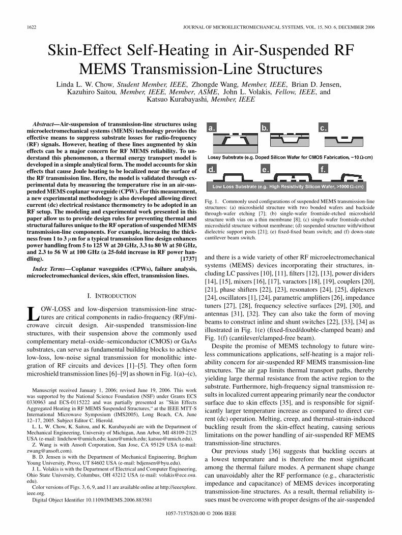
Fig. 1. Commonly used configurations of suspended MEMS transmission-linestructures: (a) microshield structure with two bonded wafers and backsidethrough-wafer etching [7]; (b) single-wafer frontside-etched microshieldstructure with vias on a thin membrane [8]; (c) single-wafer frontside-etchedmicroshield structure without membrane; (d) suspended structure with/withoutdielectric support posts [21]; (e) fixed-fixed beam switch; and (f) down-statecantilever beam switch.
and there is a wide variety of other RF microelectromechanicalsystems (MEMS) devices incorporating their structures, in-cluding LC passives [10], [11], filters [12], [13], power dividers[14], [15], mixers [16], [17], varactors [18], [19], couplers [20],[21], phase shifters [22], [23], resonators [24], [25], diplexers[24], oscillators [1], [24], parametric amplifiers [26], impedancetuners [27], [28], frequency selective surfaces [29], [30], andantennas [31], [32]. They can also take the form of movingbeams to construct inline and shunt switches [22], [33], [34] asillustrated in Fig. 1(e) (fixed-fixed/double-clamped beam) andFig. 1(f) (cantilever/clamped-free beam).
Despite the promise of MEMS technology to future wire-less communications applications, self-heating is a major reli-ability concern for air-suspended RF MEMS transmission-linestructures. The air gap limits thermal transport paths, therebyyielding large thermal resistance from the active region to thesubstrate. Furthermore, high-frequency signal transmission re-sults in localized current appearing primarily near the conductorsurface due to skin effects [35], and is responsible for signif-icantly larger temperature increase as compared to direct cur-rent (dc) operation. Melting, creep, and thermal-strain-inducedbuckling result from the skin-effect heating, causing seriouslimitations on the power handling of air-suspended RF MEMStransmission-line structures.
Our previous study [36] suggests that buckling occurs ata lowest temperature and is therefore the most significantamong the thermal failure modes. A permanent shape changecan unavoidably alter the RF performance (e.g., characteristicimpedance and capacitance) of MEMS devices incorporatingtransmission-line structures. As a result, thermal reliability is-sues must be overcome with proper designs of the air-suspended
1057-7157/$20.00 © 2006 IEEE

CHOW et al.: SKIN-EFFECT SELF-HEATING IN AIR-SUSPENDED RF MEMS TRANSMISSION-LINE STRUCTURES 1623
TABLE ICANDIDATES OF SOME MICRON-RESOLUTION TEMPERATURE
MEASUREMENT TECHNIQUES
transmission-line structures. Previous work in power handlingstudies of RF MEMS switches include RF self-biasing [37],electromigration of electroplated gold [38], localized heatingsimulations [36], [39], and measurement using electro-op-tothermal probes [25]. However, limited research has beenperformed to systematically investigate the impact of skineffects on self-heating and thermal reliability of suspended RFMEMS transmission-line structures. It should be noted thatsputtered gold structures have at least three times better resis-tance to electromigration with maximum sustainable currentdensity of 20–35 GA/m in 150 C [41] than electroplated oneswith maximum sustainable current density of 6 GA/m [38].This requires us to carefully consider other failure mechanismsthan electromigration for RF MEMS transmission-line struc-tures made of sputtered gold.
Table I summarizes candidate techniques for MEMS-scalethermal characterization. Among them, we identify dc electricalresistance thermometry (based on the four-wire measurementtechnique [42]) as the most suitable approach for fast and accu-rate temperature sensing required in our paper. In general, thefour-wire measurement technique can be implemented withoutsophisticated equipment and difficult calibration procedures[43]. This technique has limited spatial resolution as comparedto other scanning thermal probe methods.
As shown later, the device of our interest is found to fail bybuckling before local creep or melting occurs. Buckling is moreaffected by the overall device temperature increase than by thepeak local temperature. Therefore, we believe that dc electricalresistance thermometry is most promising for our study as itprovides quantitative information on the spatially averaged de-vice temperature. To our knowledge, no previous work demon-strated use of this technique for thermal characterization of RFMEMS devices. In this paper, we propose a new experimental
methodology to adopt dc electrical resistance thermometry forRF applications.
Specifically, this paper studies the thermal behavior of air-suspended RF MEMS coplanar waveguide (CPW) transmissionlines experiencing self-heating due to skin effects, which limitstheir power handling capability. We apply both modeling andexperimental methods to demonstrate the frequency-dependenttemperature increase at various RF power levels. The approachthat we adopt here is based on our recent preliminary researchdevelopments [44]. This paper extends them to obtain more in-sight into design rules.
First, we use our previous model integrating full-waveelectromagnetics with heat conduction theory to design thedimensions of MEMS transmission lines [45]–[47]. We thenproceed to show that a drastically simplified electrothermalmodel leading to a closed-form analytical solution can yieldsimilar simulation results as compared to the vigorous model.Subsequently, we develop an in situ experimental techniqueto measure the temperature of RF MEMS transmission linesto validate our models. Last, using the experimentally vali-dated analytical model, we predict the upper bound for powerhandling of RF MEMS transmission lines of varying dimen-sions and materials. The model and experimental techniquedeveloped in this paper can guide the design of RF MEMScomponents with improved thermal reliability and power han-dling.
II. MODELING APPROACHES
A. EM EFE–BI-Coupled Thermal FEM Simulation
To accurately account for all electrical losses in the suspendedstructure, we first carried out a full-wave electromagnetic (EM)simulation using the extended finite element–boundary integral(EFE–BI) method with a preconditioner [47]. The heat conduc-tion equation can then be solved via a two-dimensional (2-D)thermal finite element model to evaluate the heat source den-sity [36], [45], [46]. This integrated modeling is very accuratein capturing all the electromagnetic effects including losses dueto substrate, surface radiation, and current crowding at the widthedges, namely, the edge effect. However, the resulting solutionmatrix is highly ill-conditioned for such small MEMS dimen-sions ( 0.001 wavelength), requiring half an hour processingtime on a Pentium PC with a good preconditioner. This moti-vates us to explore an analytical model to minimize computa-tional requirements for device design.
B. Analytical Thermal Model for Skin Effects
Our simulations show that on a typical ( 100 m wide)MEMS transmission-line structure, the edge effects and elec-tromagnetic radiation loss at its top surface are minimal ascompared to the skin effect even at frequencies above 100 GHz.It is also shown that the spatial variation of the current concen-trated within the skin depth is negligibly small. As such, weproceed to develop a thermal model that only captures the skineffect, as in Fig. 3, and approximate the RF equivalent currentdistribution to be uniform. Accordingly, the RF power deliveredto the load is given by , where is thecharacteristic line impedance, and denotes the RF current.

1624 JOURNAL OF MICROELECTROMECHANICAL SYSTEMS, VOL. 15, NO. 6, DECEMBER 2006
Fig. 2. Schematic diagram for our proposed analytical thermal model.
Further, we assume only one skin depth of penetration andtake the RF current density to be uniform as well. Weremark that the thickness of the suspended beam is designedto always be at least one skin-depth thick. Specifically, a2.7- m-thick beam is 1.1 times the skin depth of 2.4 m at2 GHz, 2.9 times (skin depth is 0.93 m) at 13.5 GHz, and3.4 times (skin depth is 0.8 m) at 18 GHz. Taking the ratioof the power used in our model to the total power dissipatedin a semi-infinite conductor, we can then estimate the modelerrors to be 11%, 0.30%, and 0.11% at 2, 13.5, and 18 GHz,respectively. That is, the largest error is at 2 GHz, and as thefrequency increases the error becomes negligible. Further, sincemost of the transmission-line structures have uniform width
and the major objective of the paper is to provide simpleanalytical formulae (as compared to numerical simulations) wecan resort to these one-dimensional (1-D) models. As expected,the simplified analytical formulae will serve to aid thermaldesign rules and to allow for material property sensitivitystudies with fewer computational requirements while capturingthe essential physics. Our simulations show that on a typical( 100 m wide) MEMS transmission-line structure, the edgeeffects and electromagnetic radiation loss at its top surface areminimal as compared to the skin effect even at frequency above100 GHz. It is also shown that the spatial variation of currentconcentrated within the skin depth is negligibly small. As such,we proceed to develop a thermal model that only captures theskin effect, as in Fig. 2, and approximate RF equivalent cur-rent distribution to be uniform. According to the zeroth-orderRF-simulation approach, the RF power delivered to the load isgiven by , where is the characteristicline impedance and is the RF equivalent current.
In most MEMS structures, conduction is the dominant heattransfer mode as compared to convection and radiation, whichconstitute less than 1% of the total heat transfer due to theirsmall surface areas. In this case, the main conductive paths forheat dissipation are across the gold suspended structure (withthermal conductivity and thickness ) and through theair gap under the suspended structure.
With the aforementioned assumptions, we begin the thermalcharacterization by considering a steady-state heat conductiongoverning equation
(1)
subject to the boundary conditions
(2)
A zero-heat-flux boundary condition is applied at the middle ofthe suspended structure because of its geometrical symmetry,and the temperatures at the both ends of the structure are as-signed to be ambient temperature. The latter boundary condi-tion is based on our measurement using a thermocouple thatshows a negligible increase in the temperature at the device an-chor regions during the thermal characterization described inSection III. We believe that it is because the gold metallizationand the RF probes could both well serve for heat spreading andheat sinking in our device thermal characterization. The sus-pended structure length and the thermal conductivities of thematerials and are assumed constant with temperature.Further, the effective current density and the resistivityare given by
(3)
(4)
where we assume a linear variation with temperature. In (4),is the temperature coefficient of resistivity (TCR) and is theelectrical resistivity at the ambient temperature.
The skin depth varies with frequency as [35]
(5)
where , H/m, is the permeability of gold. Substi-tuting (3)–(5) into (1) yields
(6)
We note that and it is of interest to linearize(6), so we introduce the Taylor’s expansion
(7)
to get
(8)
Solving (8) subject to the boundary conditions in (2) leads to
(9)
where
(10)

CHOW et al.: SKIN-EFFECT SELF-HEATING IN AIR-SUSPENDED RF MEMS TRANSMISSION-LINE STRUCTURES 1625
Fig. 3. Optical image of a suspended CPW for average temperature measure-ment.
and
(11)
From this result, we note that the peak/maximum temperaturerise is at the middle of the beam, and is given by
(12)
with the corresponding average temperature rise across the sus-pended structure given by
(13)
In Section III, we describe experiments designed to validate thisclosed-form thermal model and to generate design rules.
III. EXPERIMENTS
Among various types of transmission lines such as mi-crostrip and slot lines, CPWs are popular in use because theydo not add additional inductance at the RF ground. We canalso readily measure the RF performance directly using RFground–signal–ground (G–S–G) probes without adapting addi-tional connectors. Therefore, we will employ the CPW designfor the MEMS structure, as shown in Fig. 3.
A. Micron Resolution DC-RF Decoupled In Situ TemperatureMeasurement Technique Development
Our four-wire measurement configuration is implemented byadding four on-chip inductive transmission lines at the two endsof the signal line of the suspended CPW. The basic tempera-ture sensing mechanism is as follows: With RF power passingthrough it, the suspended CPW heats up, accompanied by alinear rise in electrical resistivity with temperature. The sub-ject-suspended CPW is also fed with a small dc current and thecorresponding dc voltage is measured. The average temperature
Fig. 4. Fabrication process of the suspended CPW and the ground (GND)tunnel for RF inductive lines.
rise of the entire suspended CPW is then obtained through pre-cisely extracting the change in resistivity from the measured dcvoltage and applied dc current. It is important to note that the dccurrent adds negligible power towards temperature rise ( 1%)during the RF operation.
With some design care, we can achieve high accuracy in thetemperature extraction process. As both dc and RF power arepresent, the dc and RF circuits must be decoupled from eachother. This is achieved using the on-chip RF inductive transmis-sion lines and an off-chip dc blocking capacitor. The on-chipinductors were chosen because they are small and compact, andthey eliminate losses due to off-chip wiring. Also, the off-chipblocking capacitors were chosen to avoid large parasitic capaci-tance with the substrate and CPW ground lines, and because anon-chip capacitor would be quite large.
B. Device Design and Fabrication
We designed the RF MEMS suspended CPW transmissionlines with a four-wire thermometric circuitry to yield minimumreturn loss and insertion loss . The designs of purely sus-pended CPWs were first based on a closed-form conformal map-ping method and the commercial software: ADS Momentum2003A (Agilent). The four-wire temperature sensing circuitsthat included inductive lines as RF chokes and probe pads werethen added to the suspended CPW structure. Prior to doing so,we used IE3D 10.0 (Zeland) to ensure that it blocks RF signals.
Most microwave components are made of gold to achievelow resistivity and inertness to oxidation. The suspended CPWtransmission lines tested here were fabricated using gold surfacemicromachining. It should be noted, however, that this temper-ature measurement technique can be applicable to any electri-cally conductive material such as aluminum and copper.
A 30-nm Cr/1- m-Au thin film was initially sputtered on aglass substrate and lithographically patterned the probe pads andfour inductive lines, as shown in Fig. 4. A photoresist sacrificiallayer of 3 m was then spun-on to define the anchor. Also, a2.7- m-Au thin film was sputtered as the suspended CPW signallines, and the ground tunnel above the four inductive lines. Afterthe suspended structures were patterned and wet-etched, we pro-ceeded with die-sawing, sacrificial layer removal, and finallyCO critical dry. In total, this process requires only three masks.
C. Setup and Calibration
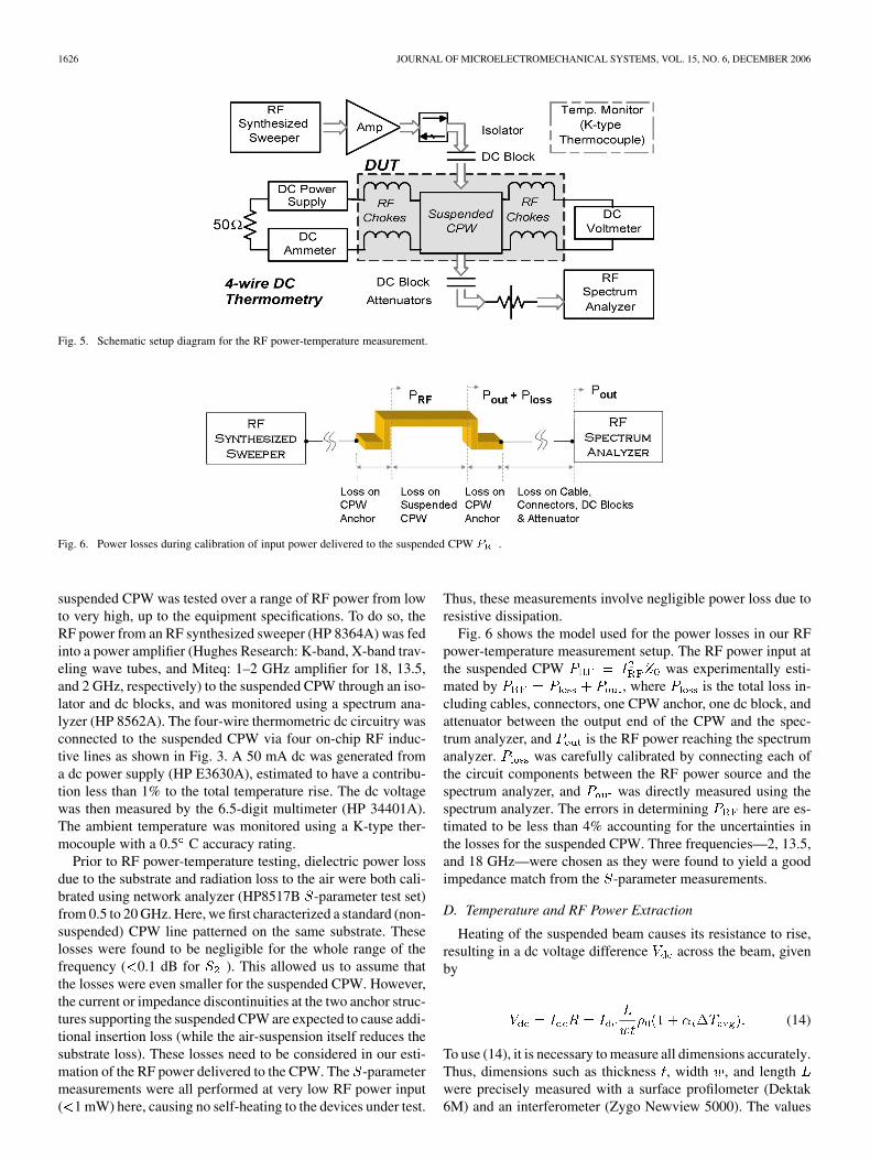
Fig. 5 shows the experimental setup for our RF power-tem-perature measurements. To maximize thermal sensitivity, the
1626 JOURNAL OF MICROELECTROMECHANICAL SYSTEMS, VOL. 15, NO. 6, DECEMBER 2006
Fig. 5. Schematic setup diagram for the RF power-temperature measurement.
Fig. 6. Power losses during calibration of input power delivered to the suspended CPW P .
suspended CPW was tested over a range of RF power from lowto very high, up to the equipment specifications. To do so, theRF power from an RF synthesized sweeper (HP 8364A) was fedinto a power amplifier (Hughes Research: K-band, X-band trav-eling wave tubes, and Miteq: 1–2 GHz amplifier for 18, 13.5,and 2 GHz, respectively) to the suspended CPW through an iso-lator and dc blocks, and was monitored using a spectrum ana-lyzer (HP 8562A). The four-wire thermometric dc circuitry wasconnected to the suspended CPW via four on-chip RF induc-tive lines as shown in Fig. 3. A 50 mA dc was generated froma dc power supply (HP E3630A), estimated to have a contribu-tion less than 1% to the total temperature rise. The dc voltagewas then measured by the 6.5-digit multimeter (HP 34401A).The ambient temperature was monitored using a K-type ther-mocouple with a 0.5 C accuracy rating.
Prior to RF power-temperature testing, dielectric power lossdue to the substrate and radiation loss to the air were both cali-brated using network analyzer (HP8517B -parameter test set)from 0.5 to 20 GHz. Here, we first characterized a standard (non-suspended) CPW line patterned on the same substrate. Theselosses were found to be negligible for the whole range of thefrequency ( 0.1 dB for ). This allowed us to assume thatthe losses were even smaller for the suspended CPW. However,the current or impedance discontinuities at the two anchor struc-tures supporting the suspended CPW are expected to cause addi-tional insertion loss (while the air-suspension itself reduces thesubstrate loss). These losses need to be considered in our esti-mation of the RF power delivered to the CPW. The -parametermeasurements were all performed at very low RF power input( 1 mW) here, causing no self-heating to the devices under test.
Thus, these measurements involve negligible power loss due toresistive dissipation.
Fig. 6 shows the model used for the power losses in our RFpower-temperature measurement setup. The RF power input atthe suspended CPW was experimentally esti-mated by , where is the total loss in-cluding cables, connectors, one CPW anchor, one dc block, andattenuator between the output end of the CPW and the spec-trum analyzer, and is the RF power reaching the spectrumanalyzer. was carefully calibrated by connecting each ofthe circuit components between the RF power source and thespectrum analyzer, and was directly measured using thespectrum analyzer. The errors in determining here are es-timated to be less than 4% accounting for the uncertainties inthe losses for the suspended CPW. Three frequencies—2, 13.5,and 18 GHz—were chosen as they were found to yield a goodimpedance match from the -parameter measurements.
D. Temperature and RF Power Extraction
Heating of the suspended beam causes its resistance to rise,resulting in a dc voltage difference across the beam, givenby
(14)
To use (14), it is necessary to measure all dimensions accurately.Thus, dimensions such as thickness , width , and lengthwere precisely measured with a surface profilometer (Dektak6M) and an interferometer (Zygo Newview 5000). The values
CHOW et al.: SKIN-EFFECT SELF-HEATING IN AIR-SUSPENDED RF MEMS TRANSMISSION-LINE STRUCTURES 1627
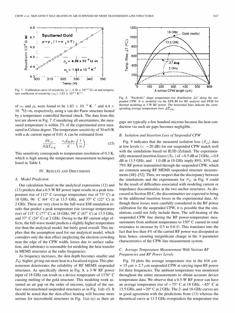
Fig. 7. Calibration curve of resistivity (� ), 4.38 � 10 �m and tempera-ture coefficient of resistivity (� ), 1.83 � 10 K .
of and were found to be 1.83 10 K and 4.410 m, respectively, using a van der Pauw structure heatedby a temperature controlled thermal chuck. The data from thistest are shown in Fig. 7. Considering all uncertainties, the mea-sured temperature is within 2% of the experimental error mea-sured in Celsius degree. The temperature sensitivity of 30 mV/Kwith a dc current input of 0.01 A can be estimated from
(15)
This sensitivity corresponds to temperature resolution of 0.3 K,which is high among the temperature measurement techniqueslisted in Table I.
IV. RESULTS AND DISCUSSIONS
A. Model Prediction
Our calculation based on the analytical expressions (12) and(13) predicts that a 0.5-W RF power input results in a peak tem-perature rise of 112 C (average temperature rise of 73 C) at18 GHz, 96 C (64 C) at 13.5 GHz, and 35 C (22 C) at2 GHz. These are very close to the full-wave EM simulation re-sults that predict a peak temperature rise (average temperaturerise) of 115 C (77 C) at 18 GHz, 99 C (67 C) at 13.5 GHz,and 37 C (24 C) at 2 GHz. Owing to the RF current edge ef-fects, the full-wave model predicts a slightly higher temperaturerise than the analytical model, but fairly good overall. This im-plies that the assumption used for our analytical model, whichconsiders only the skin effect (neglecting the electron crowdingnear the edge of the CPW width, losses due to surface radia-tion, and substrate) is reasonable for modeling the heat transferin MEMS structures at the radio frequencies.
As frequency increases, the skin depth becomes smaller andhigher, giving out more heat in a localized region. This phe-
nomenon deteriorates the reliability of RF MEMS suspendedstructures. As specifically shown in Fig. 8, a 3-W RF powerinput of 18 GHz can result in a device temperature of 1376 Ccausing melting of the gold structure. This modeling work as-sumed an air gap on the order of microns, typical of the sur-face-micromachined suspended structures as in Fig. 1(d)–(f). Itshould be noted that the skin-effect heating will become moreserious for microshield structures in Fig. 1(a)–(c) as their air
Fig. 8. “Parabolic” shape temperature-rise distribution �T along the sus-pended CPW. It is modeled via the EFE-BI for RF analysis and FEM forthermal modeling at 3-W RF power. The horizontal lines indicate the corre-sponding average temperature rises �T .
gaps are typically a few hundred microns because the heat con-duction via such air gaps becomes negligible.
B. Isolation and Insertion Loss of Suspended CPW
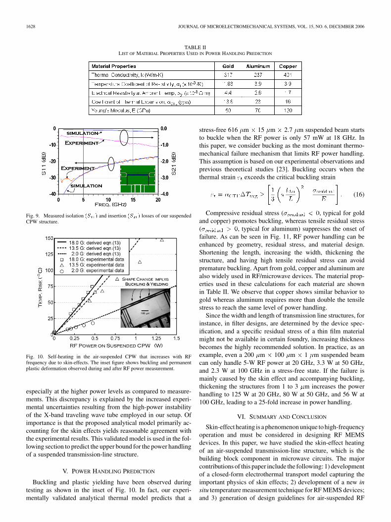
Fig. 9 indicates that the measured isolation loss dataat low levels ( 20 dB) for our suspended CPW match wellwith the simulations based on IE3D (Zeland). The experimen-tally measured insertion losses of 0.5 dB at 2 GHz, 0.8dB at 13.5 GHz, and 1.0 dB at 18 GHz imply 89%, 83%, and79% RF power transmitted through the suspended CPW, whichare common among RF MEMS suspended structure measure-ments [48]–[52]. Thus, we suspect that the discrepancy betweenthe simulations and the experiments for in Fig. 9 couldbe the result of difficulties associated with modeling current orimpedance discontinuities at the two anchor structures. As dis-cussed in Section III-C, the discontinuities are expected to bringin the additional insertion losses in the experimental data. Al-though these losses were carefully considered in the RF powercalibration for the suspended CPW, it is possible that the sim-ulations could not fully include them. The self-heating of thesuspended CPW line during the RF power-temperature mea-surements from ambient temperature to 150 C caused its totalresistance to increase by 0.5 to 0.6 . This translates into thefact that less than 4% of the carried RF power was dissipated asheat, hence, ensuring insignificant change in the -parametercharacteristics of the CPW line measurement system.
C. Average Temperature Measurement With Various RFFrequencies and RF Power Levels
Fig. 10 plots the average temperature rise in the 616 m15 m 2.7 m suspended CPW at varying input RF power
for three frequencies. The ambient temperature was monitoredthroughout the entire measurements to obtain accurate devicetemperature data. We observe that a 0.5-W RF power can havean average temperature rise of 75 C at 18 GHz, 65 C at13.5 GHz, and 20 C at 2 GHz. The 2- and 18-GHz curves arein good agreement with the predictions from (13) whereas thetheoretical curve at 13.5 GHz overpredicts the temperature rise
1628 JOURNAL OF MICROELECTROMECHANICAL SYSTEMS, VOL. 15, NO. 6, DECEMBER 2006
TABLE IILIST OF MATERIAL PROPERTIES USED IN POWER HANDLING PREDICTION
Fig. 9. Measured isolation (S ) and insertion (S ) losses of our suspendedCPW structure.
Fig. 10. Self-heating in the air-suspended CPW that increases with RFfrequency due to skin-effects. The inset figure shows buckling and permanentplastic deformation observed during and after RF power measurement.
especially at the higher power levels as compared to measure-ments. This discrepancy is explained by the increased experi-mental uncertainties resulting from the high-power instabilityof the X-band traveling wave tube employed in our setup. Ofimportance is that the proposed analytical model primarily ac-counting for the skin effects yields reasonable agreement withthe experimental results. This validated model is used in the fol-lowing section to predict the upper bound for the power handlingof a suspended transmission-line structure.
V. POWER HANDLING PREDICTION
Buckling and plastic yielding have been observed duringtesting as shown in the inset of Fig. 10. In fact, our experi-mentally validated analytical thermal model predicts that a
stress-free 616 m 15 m 2.7 m suspended beam startsto buckle when the RF power is only 57 mW at 18 GHz. Inthis paper, we consider bucking as the most dominant thermo-mechanical failure mechanism that limits RF power handling.This assumption is based on our experimental observations andprevious theoretical studies [23]. Buckling occurs when thethermal strain exceeds the critical buckling strain
(16)
Compressive residual stress ( , typical for goldand copper) promotes buckling, whereas tensile residual stress( , typical for aluminum) suppresses the onset offailure. As can be seen in Fig. 11, RF power handling can beenhanced by geometry, residual stress, and material design.Shortening the length, increasing the width, thickening thestructure, and having high tensile residual stress can avoidpremature buckling. Apart from gold, copper and aluminum arealso widely used in RF/microwave devices. The material prop-erties used in these calculations for each material are shownin Table II. We observe that copper shows similar behavior togold whereas aluminum requires more than double the tensilestress to reach the same level of power handling.
Since the width and length of transmission line structures, forinstance, in filter designs, are determined by the device spec-ification, and a specific residual stress of a thin film materialmight not be available in certain foundry, increasing thicknessbecomes the highly recommended solution. In practice, as anexample, even a 200 m 100 m 1 m suspended beamcan only handle 5-W RF power at 20 GHz, 3.3 W at 50 GHz,and 2.3 W at 100 GHz in a stress-free state. If the failure ismainly caused by the skin effect and accompanying buckling,thickening the structures from 1 to 3 m increases the powerhandling to 125 W at 20 GHz, 80 W at 50 GHz, and 56 W at100 GHz, leading to a 25-fold increase in power handling.
VI. SUMMARY AND CONCLUSION
Skin-effect heating is a phenomenon unique to high-frequencyoperation and must be considered in designing RF MEMSdevices. In this paper, we have studied the skin-effect heatingof an air-suspended transmission-line structure, which is thebuilding block component in microwave circuits. The majorcontributions of this paper include the following: 1) developmentof a closed-form electrothermal transport model capturing theimportant physics of skin effects; 2) development of a new insitu temperature measurement technique for RF MEMS devices;and 3) generation of design guidelines for air-suspended RF

CHOW et al.: SKIN-EFFECT SELF-HEATING IN AIR-SUSPENDED RF MEMS TRANSMISSION-LINE STRUCTURES 1629
Fig. 11. Power handling prediction using the proposed closed-form analytical model with various geometry, material, and residual stress: (a) length, (b) width,(c) thickness, (d) gold, (e) copper, and (f) aluminum.
MEMS transmission-line structures to improve power handlingand reliability.
The RF MEMS CPW structure dimensions in our experi-ments we designed using our previous full-wave electromag-netic numerical model using the EFE–BI method, coupled witha finite element thermal simulation. The results from these vig-orous simulations and those from the closed-form analyticalmodel show that the skin effects have the largest impact onself-heating. That is, the two models predict nearly the samevalues for the maximum and average temperature rises within
2% difference. Undeniably, the analytical model has the ad-vantage of significantly less computational requirements.
The developed new experimental technique to accuratelymeasure the spatially averaged temperature of the testing CPWstructure incorporated a RF-dc decoupled thermometric circuit.This allows for in situ electrical resistance thermometry of theRF MEMS components based on the four-wire measurementtechnique. The obtained experimental results showed that thetemperature increase is a strong function of frequency and givesrise to thermal-stress-induced structural instability and perma-nent shape change. Further, the obtained data show reasonablygood agreement with our model predictions.
Using the experimentally validated model, we have investi-gated the influence of RF MEMS design parameters, includingwidth, length, thickness, material properties, and residual stresson the RF power handling subject to buckling failure criteria.Most often, device specifications and process conditions im-pose limited flexibility in the width and length of transmissionline structures, and in the control of residual stress. Therefore,
increasing the transmission-line thickness is the most practicaldesign approach to maximizing the power handling. In one ex-ample, an increase of the thickness by 2 m can substantiallydecrease temperature rise and thus permits the air-suspended RFMEMS CPW to transmit greater than 25-fold more RF power.
ACKNOWLEDGMENT
The authors would like to thank Dr. B. J. J. Hung and Prof. G.M. Rebeiz from the University of Michigan Terahertz IntegratedCircuit Lab for helpful assistance and fruitful discussions on RFpower experiments.
REFERENCES
[1] E.-C. Park and E. Yoon, “A 13 GHz CMOS distributed oscillator usingMEMS coupled transmission lines for low phase noise,” in Proc. IEEEInt. Solid-State Circuit Conf., 2004, vol. 1, pp. 300–301, pt. 1.
[2] L. E. Larson, R. H. Hackett, M. A. Melendes, and R. F. Lohr, “Mi-cromachined microwave actuator (MIMAC) technology-a new tuningapproach for microwave integrated circuits,” in Proc. IEEE Microw.Millimeter-Wave Monolithic Circuits Symp. Dig., 1991, pp. 27–30.
[3] L. P. B. Katehi, G. M. Rebeiz, T. M. Weller, R. F. Drayton, H.-J. Cheng,and J. F. Whitaker, “Micromachined circuits for millimeter- and sub-millimeter-wave applications,” IEEE Antennas Propagat. Mag., vol.35, no. 5, pp. 9–17, Oct. 1993.
[4] C. T.-C. Nguyen, L. P. B. Katehi, and G. M. Rebeiz, “Micromachineddevices for wireless communications,” Proc. IEEE, vol. 86, no. 8, pp.1756–1768, Aug. 1998.
[5] H. A. C. Tilmans, W. De Raedt, and E. Beyne, “MEMS for wirelesscommunications: From RF-MEMS components to RF-MEMS-SiP,” J.Micromech. Microeng., vol. 13, no. 4, pp. S139–S163, Jul. 2003.
[6] A. G. Engel and L. P. B. Katehi, “Low-loss monolithic transmissionlines for submillimeter and terahertz frequency applications,” IEEETrans. Microw. Theory Tech., vol. 39, no. 11, pp. 1847–1854, Nov.1991.
1630 JOURNAL OF MICROELECTROMECHANICAL SYSTEMS, VOL. 15, NO. 6, DECEMBER 2006
[7] N. I. Dib, W. P. Harokopus, Jr., P. B. Katehi, C. C. Ling, and G. M. Re-beiz, “Study of a novel planar transmission line,” in Proc. IEEE MTT-SInt. Microw. Symp. Dig., 1991, vol. 2, pp. 623–626.
[8] Y. Yoshida, T. N. Nishino, J. Jiao, S.-S. Lee, Y. Suehiro, K. Miyaguchi,T. Fukami, M. Kimata, and O. Ishima, “A grounded coplanar wave-guide with a metallized silicon cavity fabricated by front-surface-onlyprocesses,” Sens. Actuators A: Phys., vol. 111, no. 1, pp. 129–134,2004.
[9] S. Chen and Y. Liu, “Analysis and calculation of the micro-shield line,”Tien Tzu Hsueh Pao/Acta Electronica Sinica, vol. 26, no. 6, pp. 71–73,1998, 81.
[10] C.-Y. Chi and G. M. Rebeiz, “Planar millimeter microstrip lumped el-ements using micro-machining techniques,” in Proc. IEEE MTT-S Int.Microw. Symp. Dig., 1994, vol. 2, pp. 657–660.
[11] S.-S. Lee, Y. Yoshida, T. Nishino, Y. Suehiro, and T. Fukami, “Si-multaneous implementation of various RF passives using a novel RFMEMS process module and metallized air cavity,” J. Micromech. Mi-croeng., vol. 15, no. 3, pp. 441–446, Mar. 2005.
[12] S. V. Robertson, L. P. B. Katehi, and G. M. Rebeiz, “W-band mi-croshield low-pass filter,” in Proc. IEEE MTT-S Int. Microw. Symp.Dig., 1994, vol. 2, pp. 625–628.
[13] T. Zhou and A. M. Robinson, “Tunable CMOS MEMS electromechan-ical bandpass filters,” Can. J. Electr. Comput. Eng., vol. 27, no. 1, pp.17–21, Jan. 2002.
[14] T. M. Weller, L. P. B. Katehi, M. I. Herman, and P. D. Warnhof,“Membrane Technology (MIST-T) applied to microstrip: A 33 GHzWilkinson power divider,” in Proc. IEEE MTT-S Int. Microw. Symp.Dig., 1994, vol. 2, pp. 911–914.
[15] M. Unlu, K. Topalli, H. Sagkol, S. Demir, O. A. Civi, S. S. Koc, andT. Akin, “RF MEMS adjustable impedance matching network and ad-justable power divider,” in Proc. IEEE Antennas Propagat. Int. Symp.,2002, vol. 2, pp. 26–29.
[16] T.-H. Lee, J. R. East, C.-Y. Chi, G. M. Rebeiz, R. J. Dengler, P. H.Siegel, and G. I. Haddad, “The fabrication and performance of planardoped barrier diodes as 200 GHz subharmonically pumped mixers,”IEEE Trans. Microw. Theory Tech., vol. 42, no. 4, pp. 742–749, Apr.1994.
[17] T. Buck, M. Reimann, M. Ulm, R. Mueller-Fiedler, J. Seidel, E. Kasper,C. Schoellhorn, and S. Haak, “Monolithic integration of RF-MEMSand semiconductor devices for the K-band,” Proc. SPIE-Int. Soc. Opt.Eng., vol. 4981, pp. 131–138, 2003.
[18] D. J. Young and B. E. Boser, “A micromachined variable capacitorfor monolithic low-noise VCOs,” in Proc. Solid-State Sens. ActuatorsWorkshop, Jun. 1996, pp. 86–89.
[19] Z.-W. Liu, J. Wei, Y. Wang, J. Fang, L.-T. Liu, and Z.-J. Li,“Analysis and optimization of a side pull-down electrodes controlledMEMS varactor,” Opt. Precision Eng., vol. 13, no. 2, pp. 135–143,Apr. 2005.
[20] S. V. Robertson, L. P. B. Katehi, and G. M. Rebeiz, “A 10–50 GHzmicromachined directional coupler,” in Proc. IEEE MTT-S Int. Microw.Symp. Dig., 1996, vol. 2, pp. 797–800.
[21] S.-C. Kim, B.-S. Ko, T.-J. Baek, B.-O. Lim, A. Dan, D.-H. Shin, andJ.-K. Rhee, “Hybrid ring coupler for W-band MMIC applications usingMEMS technology,” IEEE Microw. Wireless Compon. Lett., vol. 15, no.10, pp. 652–654, Oct. 2005.
[22] N. S. Barker and G. M. Rebeiz, “Distributed MEMS true-time delayphase shifters and wide-band switches,” IEEE Trans.Microw. TheoryTech., vol. 46, no. 11, pp. 1881–1890, Nov. 1998.
[23] G. McFeetors and M. Okoniewski, “Analog tunable microwave phaseshifters using RF MEMS,” in Proc. Int. Symp. Antenna Tech. Appl.Electromagn. and Int. Sci. Radio Union (URSI) Conf., 2004, pp. 29–32.
[24] A. R. Brown and G. M. Rebeiz, “Micromachined high-Q resonators,low-loss diplexers, and low phase-noise oscillators for a 28 GHz front-end,” in Proc. IEEE Radio Wireless Conf. (RAWCON99), 1999, pp.247–253.
[25] E. Larique, P. Blondy, M. Chatras, D. Mercier, D. Cros, L. Basteres,and B. Guillon, “Tunable RF MEMS resonators and filters,” Proc.SPIE-Int. Soc. Opt. Eng., vol. 4408, pp. 63–72, 2001.
[26] J.-P. Raskin, A. R. Brown, B. T. Khuri-Yakub, and G. M. Rebeiz, “Anovel parametric-effect MEMS amplifier,” J. Microelectromech. Syst.,vol. 9, no. 4, pp. 528–537, Dec. 2000.
[27] H. T. Kim, S. Jung, K. Kang, J. H. Park, Y. K. Kim, and Y. Kwon,“Low-loss analog and digital micromachined impedance tuners at theKa-band,” IEEE Trans. Microw. Theory Tech., vol. 49, pp. 2394–2400,Dec. 2001.
[28] Y. Lu, L. P. B. Katehi, and D. Peroulis, “High-power MEMSvaractors and impedance tuners for millimeter-wave applications,”IEEE Trans. Microw. Theory Tech., vol. 53, no. 11, pp. 3672–3678,Nov. 2005.
[29] A. Abbaspour-Tamijani, B. Schoenlinner, K. Sarabandi, and G. M.Rebeiz, “A new class of bandpass frequency selective structures,”in Proc. IEEE Antenna Propagat. Int. Symp., 2003, vol. 2, pp.817–820, pt. 2.
[30] J. P. Gianvittorio, J. Zendejas, Y. Rahmat-Samii, and J. W. Judy,“MEMS enabled reconfigurable frequency selective surfaces: Design,simulation, fabrication, and measurement,” in Proc. IEEE AntennasPropagat. Soc. Int. Symp., 2002, vol. 2, pp. 404–407, pt. 2.
[31] G. M. Rebeiz, W. G. Regehr, D. B. Rutledge, R. L. Savage, and N. C.Luhmann, Jr., “Submillimeter-wave antennas on thin membranes,” Int.J. Infrared Millimeter Waves, vol. 8, no. 10, pp. 1249–1255, Oct. 1987.
[32] J.-C. Chiao, Y. Fu, I. M. Chio, M. DeLisio, and L.-Y. Lin, “MEMSreconfigurable Vee antenna,” in Proc. IEEE MTT-S Int. Microw. Symp.Dig., 1999, vol. 4, pp. 1515–1518, pt. 4.
[33] C. L. Goldsmith, J. Randall, S. Esbelman, T. H. Lin, D. Denniston,S. Chen, and B. Norvell, “Characteristics of micromachined switchesat microwave frequencies,” in Proc. IEEE MTT-S Int. Microw. Symp.Dig., Jun. 1996, vol. 2, pp. 1141–1144.
[34] A. B. Yu, A. Q. Liu, Q. X. Zhang, A. Alphones, and H. M. Hosseini,“Micromachined DC contact capacitive switch on low-resistivity sil-icon substrate,” Sens. Actuators A: Phys., vol. 127, no. 1, pp. 24–30,Feb. 2006.
[35] H. Lamb, “On electrical motions in a spherical conductor,” Philos.Trans. London Roy. Soc. (II), vol. 174, pp. 519–549, 1883.
[36] Z. Wang, B. D. Jensen, L. L. W. Chow, J. L. Volakis, K. Saitou, andK. Kurabayashi, “Full-wave electromagnetic and thermal modeling forprediction of heat-dissipation-induced RF MEMS switch failure,” J.Micromech. Microeng., vol. 16, pp. 157–164, 2006.
[37] X. Rottenberg, S. Brebels, W. De Raedt, B. Nauwelaers, and H. A. C.Tilmans, “RF-power: Driver for electrostatic RF-MEMS devices,” J.Micromech. Microeng., vol. 14, pp. S43–S48, 2004.
[38] B. Ducarouge, E. Perret, F. Flourens, S. Melle, E. Ongareau, K. Gre-nier, A. Boukabache, V. Conedera, P. Pons, E. Perret, H. Aubert, andR. Plana, “Power capabilities of RF MEMS,” in Proc. 24th Int. Conf.Microelectr. (MIEL 2004), May 2004, vol. 1, pp. 65–70.
[39] J. B. Rizk, E. Chaiban, and G. M. Rebiez, “Steady state thermal anal-ysis and high-power reliability considerations of RF MEMS capacitiveswitches,” in Proc. IEEE MTT-S Int. Microw. Symp. Dig., 2002, vol. 1,pp. 239–243.
[40] R. M. Reano, D. Peroulis, J. F. Whitaker, and L. P. B. Katehi, “Electro/thermal measurements of RF MEMS capacitive switches,” in Proc.IEEE MTT-S Int. Microw. Symp. Dig., 2003, vol. 3, pp. 1923–1926.
[41] J. C. Blair, C. R. Fuller, P. B. Ghate, and C. T. Haywood, “Electromi-gration-induced failures in, and microstructure and resistivity of, sput-tered gold films,” J. Appl. Phys., vol. 43, no. 2, pp. 307–311, Feb. 1972.
[42] J. Semancik, “4-wire measurement,” Sensors, vol. 18, no. 5, pp. 44–50,1991.
[43] C. W. Lewis, “Four-wire techniques minimize temperature measure-ment errors,” InTech, vol. 42, pp. 40–43, 1995.
[44] L. L. W. Chow, Z. Wang, B. D. Jensen, K. Saitou, J. L. Volakis, and K.Kurabayashi, “Skin effects aggregated heating in RF MEMS suspendedstructures,” presented at the IEEE MTT-S Int. Microw. Symp., LongBeach, CA, Jun. 12–17, 2005.
[45] B. D. Jensen, K. Saitou, J. L. Volakis, and K. Kurabayashi, “Fully inte-grated electrothermal multi-domain modeling of RF MEMS switches,”IEEE Microw. Wireless Compon. Lett., vol. 13, no. 9, pp. 364–366, Sep.2003.
[46] B. D. Jensen, Z. Wang, L. Chow, K. Saitou, K. Kurabayashi, and J. L.Volakis, “Integrated electrothermal modeling of RF MEMS switchesfor improved power handling capability,” presented at the IEEE TopicalConf. Wireless Commun. Technol., Honolulu, HI, Oct. 15–17, 2003.
[47] Z. Wang, B. Jensen, J. Volakis, K. Saitou, and K. Kurabayashi, “A pre-conditioner for hybrid matrices arising in RF MEMS switch analysis,”presented at the IEEE Int. Antenna Propagat. Symp., Monterey, CA,Jun. 20–26, 2004.
[48] Y. Kondoh, T. Takenaka, T. Hidaka, G. Tejima, Y. Kaneko, and M.Saitoh, “High-reliability, high-performance RF micromachined switchusing liquid metal,” J. Microelectromech. Syst., vol. 14, no. 2, pp.214–220, Apr. 2005.
[49] P. Blondy, A. Crunteanu, C. Champeaux, A. Catherinot, P. Tristant,O. Vendier, J. L. Cazaux, and L. Marchand, “Dielectric less capacitiveMEMS switches,” in Proc. IEEE MTT-S Int. Microw. Symp. Dig., 2004,pp. 573–576.
[50] L. Guan, J. K. O. Sin, H. Liu, and Z. Xiong, “A fully integrated SOI RFMEMS technology for system-on-a-chip applications,” IEEE Trans.Electron Devices, vol. 53, no. 1, pp. 167–172, Jan. 2006.
[51] N. Nishijima, J.-J. Hung, and G. M. Rebeiz, “A low-voltage high con-tact force RF-MEMS switch,” in Proc. IEEE MTT-S Int. Microw. Symp.Dig., 2004, pp. 577–580.
CHOW et al.: SKIN-EFFECT SELF-HEATING IN AIR-SUSPENDED RF MEMS TRANSMISSION-LINE STRUCTURES 1631
[52] M. Tang, A.-Q. Liu, A. Agarwal, Z.-S. Liu, and C. Lu, “A single-pole double-throw (SPDT) circuit using lateral metal-contact micro-machined switches,” Sens. Actuators A: Phys., vol. 121, pp. 187–196,2005.
Linda L. W. Chow (S’02) is currently working to-wards the Ph.D. degree in mechanical engineering atUniversity of Michigan, Ann Arbor.
She has studied RF MEMS switch design,fabrication process development, and thermal/con-tact reliability studies since Fall 2002. She wasa Teaching Assistant for two semesters, and waschosen the Best Teaching Assistant. She has au-thored/coauthored about 20 conference/journalpapers.
Miss Chow, in her master studies, developed anin situ moisture sensing chip for electronic packaging reliability testing, whichwas awarded the Best Student Paper in IEEE International Symposium on Elec-tronic Materials and Packaging (EMAP2000).
Zhongde Wang (M’04) received the M.Sc. degreein microwave/RF engineering from the University ofWaterloo, Waterloo, ON, Canada, in 2002 and thePh.D. degree in electrical engineering and computerscience from the University of Michigan, Ann Arbor,in 2005 .
In January 2005, he joined Ansoft Corporation,San Jose, CA, as an Application Engineer. Hehas published over 20 papers in journals and con-ferences. His research focuses on computationalelectromagnetics, RF MEMS structure modeling,
and antenna and microwave components optimization design.Dr. Wang was awarded the Second Grade Prize for Science and Technologies
Progress by the Chinese Electrical Ministry in 1996.
Brian D. Jensen received the B.S. and M.S. degreesin mechanical engineering from Brigham YoungUniversity, Provo, UT, in 1996 and 1998, respec-tively, and the M.S. degree in electrical engineeringand the Ph.D. degree in mechanical engineering fromthe University of Michigan, Ann Arbor, in 2004.
Since January 2005, he has been an Assistant Pro-fessor in the Mechanical Engineering Department,Brigham Young University. He was previously aPostdoctoral Fellow at the University of Michigan.Before receiving the Ph.D. degree, he worked at
Sandia National Laboratories as a Micromechanical Designer. He holds sevenU.S. patents and has authored or coauthored over 35 technical papers.
Dr. Jensen received the National Science Foundation Graduate Research Fel-lowship as well as the National Defense Science and Engineering Graduate Fel-lowship.
Kazuhiro Saitou (M’97) received the Ph.D. degreein mechanical engineering from the MassachusettsInstitute of Technology (MIT), Cambridge, in 1996.
From 1997 to 2003, he was an Assistant Professorwith the Department of Mechanical Engineering,University of Michigan, Ann Arbor, where he iscurrently an Associate Professor. His research in-terests include design automation and optimization,design for X, where X = manufacture, assembly,robustness, environment, modeling, and optimiza-tion of MEMS, and evolutionary computation in
mechanical design.Dr. Saitou is a Member of American Society of Mechanical Engineers
(ASME), Society of Manufacturing Engineers, Association for ComputingMachinery, and Sigma Xi. He is currently as an Associate Editor for IEEETRANSACTIONS ON AUTOMATION SCIENCE AND ENGINEERING and an EditorialBoard Member of the International Journal of CAD/CAM, and Genetic
Programming and Evolvable Machines. He was the recipient of the 1999CAREER Award from the National Science Foundation (NSF), and of the BestPaper Award at the 5th International Symposium on Tools and Methods ofCompetitive Engineering in 2004.
John L. Volakis (S’77–M’82–SM’89–F’96) wasborn on May 13, 1956 in Chios, Greece, and movedto the United States in 1973. He received the B.E. de-gree (summa cum laude) in 1978 from YoungstownState University, Youngstown, OH, and the M.Sc.and the Ph.D. degrees from the Ohio State University(OSU), Columbus, in 1979 and 1982, respectively,all in electrical and computer engineering.
From 1982 to 1984, he was with Rockwell Inter-national, Aircraft Division (now Boeing PhantomWorks), Lakewood, CA, and, during 1978–1982, he
was a Graduate Research Associate at the ElectroScience Laboratory, OSU.Since January 2003, he has been the Roy and Lois Chope Chair Professor ofEngineering at the OSU and also serves as the Director of the ElectroScienceLaboratory. From 1984 to 2003, he was a Professor in the Electrical Engi-neering and Computer Science Department, the University of Michigan, AnnArbor. He also served as the Director of the Radiation Laboratory, from 1998 to2000. His primary research deals with computational methods, electromagneticcompatibility and interference, design of new RF materials, multiphysicsengineering, and bioelectromagnetics. He published 220 articles in majorrefereed journals (nine of these have appeared in reprint volumes), more than300 conference papers, and ten book chapters. In addition, he coauthoredtwo books: Approximate Boundary Conditions in Electromagnetics (London,U.K.: Institution of Electrical Engineers, 1995) and Finite Element Method forElectromagnetics (Piscataway, NJ: IEEE Press, 1998). He graduated/mentoredover 40 Ph.D. and Postdoctoral student, and coauthored with them five bestpaper awards at conferences. He has also written two well-edited coursepackson introductory and advanced numerical methods for electromagnetics, andhas delivered short courses on numerical methods, antennas, and frequencyselective surfaces.
Dr. Volakis received the University of Michigan College of EngineeringResearch Excellence Award, in 1998, and the University of Michigan, De-partment of Electrical Engineering and Computer Science Service ExcellenceAward, in 2001. He is listed by ISI HighlyCited.com among the top 250 mostreferenced authors (2004, 2005). He served as an Associate Editor of the IEEETRANSACTIONS ON ANTENNAS AND PROPAGATION from 1988 to 1992, andas an Associate Editor of Radio Science, from 1994 to 1997. He chaired the1993 IEEE Antennas and Propagation Society Symposium and Radio ScienceMeeting, and cochaired the same Symposium in 2003. He was a member of theAdCom for the IEEE Antennas and Propagation Society from 1995 to 1998 andserved as the 2004 President of the IEEE Antennas and Propagation Society.He also serves as an Associate Editor for the Journal of ElectromagneticWaves and Applications, the IEEE ANTENNAS AND PROPAGATION SOCIETY
MAGAZINE, and the International Union of Radio Science (URSI) Bulletin. Heis a member of Commissions B and E of URSI.
Katsuo Kurabayashi (M’00) received the B.S.degree in precision engineering from the Universityof Tokyo, Tokyo, Japan, in 1992 and the M.S. andPh.D. degrees in materials science and engineeringwith electrical engineering minor from StanfordUniversity, Stanford, CA, in 1994 and 1998, re-spectively. His Ph.D. dissertation work focused onmeasurement and modeling of the thermal transportproperties of electronic packaging and organic ma-terials for integrated circuits under the contract withthe Semiconductor Research Corporation (SRC).
He was a Research Associate with the Department of Mechanical Engineeringat Stanford University for 12 months. In January 2000, he joined the faculty ofthe University of Michigan, Ann Arbor, where he is currently Associate Pro-fessor of Mechanical Engineering and Electrical Engineering and ComputerScience. His group at the University of Michigan studies multiphysics modelingand characterization of RF MEMS, biomolecular motor hybrid NEMS/MEMStechnology, and polymer-on-silicon strain-tunable photonic devices.
Dr. Kurabayashi received the SRC Best Paper Award, in 1998, the NationalScience Foundation (NSF) CAREER Award, in 2001, and the University ofMichigan Robert Caddell Memorial Award, in 2004.