measurement and analysis of substrate leakage current of rf mems capacitive switches
TRANSCRIPT
Microelectronics Reliability 54 (2014) 152–159
Contents lists available at SciVerse ScienceDirect
Microelectronics Reliability
journal homepage: www.elsevier .com/locate /microrel
Measurement and analysis of substrate leakage current of RF memscapacitive switches
0026-2714/$ - see front matter � 2013 Elsevier Ltd. All rights reserved.http://dx.doi.org/10.1016/j.microrel.2013.07.011
⇑ Corresponding author. Tel.: +86 2583792632x8812.E-mail address: [email protected] (L. Wang).
Y.Q. Zhu, H. Qian, L.F. Wang, L. Wang ⇑, J.Y. TangSoutheast University, Key Laboratory of MEMS of Ministry of Education, Nanjing 210096, China
a r t i c l e i n f o a b s t r a c t
Article history:Received 10 April 2013Received in revised form 28 June 2013Accepted 3 July 2013Available online 22 July 2013
This paper focused on a new direction of study on leakage current called substrate charge injection. Thesubstrate leakage current of capacitive RF micro-electro-mechanical-system (MEMS) switches was mea-sured, and the conduction mechanism was estimated. The study of the leakage current conduction mech-anisms of the substrate dielectric film shows that leakage is mainly induced by hopping conduction atlow electric fields, whereas both Schottky emission and hopping conduction may contribute to the leak-age current at high fields. The quantitative relationship between the substrate leakage current and thedielectric layer leakage current was also determined for the first time. In the case of low drive voltage(0–30 V), the substrate leakage current significantly contributes to the total leakage current. Results showthat the charging properties of the substrate should not be neglected at low drive voltage because suchproperties could significantly affect the functionality and reliability of RF MEMS switches.
� 2013 Elsevier Ltd. All rights reserved.
1. Introduction
Successful integration of capacitive RF MEMS switches and RFIC into many microwave applications was expected owing to thelow loss, low power consumption, and small size of such switches[1]. However, this integration is currently hindered by reliabilityproblems, especially the charging in the dielectric layers of capac-itive RF MEMS switches. This charging process could result in achange in the pull-in voltage and/or cause stiction, thereby limitingthe functionality of the device [2,3]. Most studies on this field havefocused on the charging of the dielectric layer (switch-dielectric),which covers the actuation electrode but does not consider thecharging in the substrate dielectric. Reports have been made onsubstrate charging as a potential factor to consider in evaluatingthe failure mechanisms of MEMS [4], and further investigationhas been performed for both high-resistivity oxidized silicon andAF-45 glass substrates [5,6]. However, no clear conclusion existson the proportion of these two kinds of charge injection, whichsimultaneously affect the lifetime of the switch at the down stateof MEMS switches. Moreover, Poole–Frenkel conduction throughthe switch dielectric could be responsible for the charging mecha-nism, but the conduction mechanism of the substrate dielectric hasnot been investigated. This mechanism is important for under-standing the charging process in substrate materials. In this paper,we present a study on substrate charging by measuring the sub-strate leakage current of capacitive RF MEMS switches. The con-duction mechanism of the substrate leakage current has been
estimated. The quantitative relationship between the substratecharge injection and the dielectric layer charge injection wasinvestigated for the first time. Experimental results indicated thatsubstrate charging should be considered in the failure mechanismat low drive voltage.
2. Experiment
2.1. Test samples description
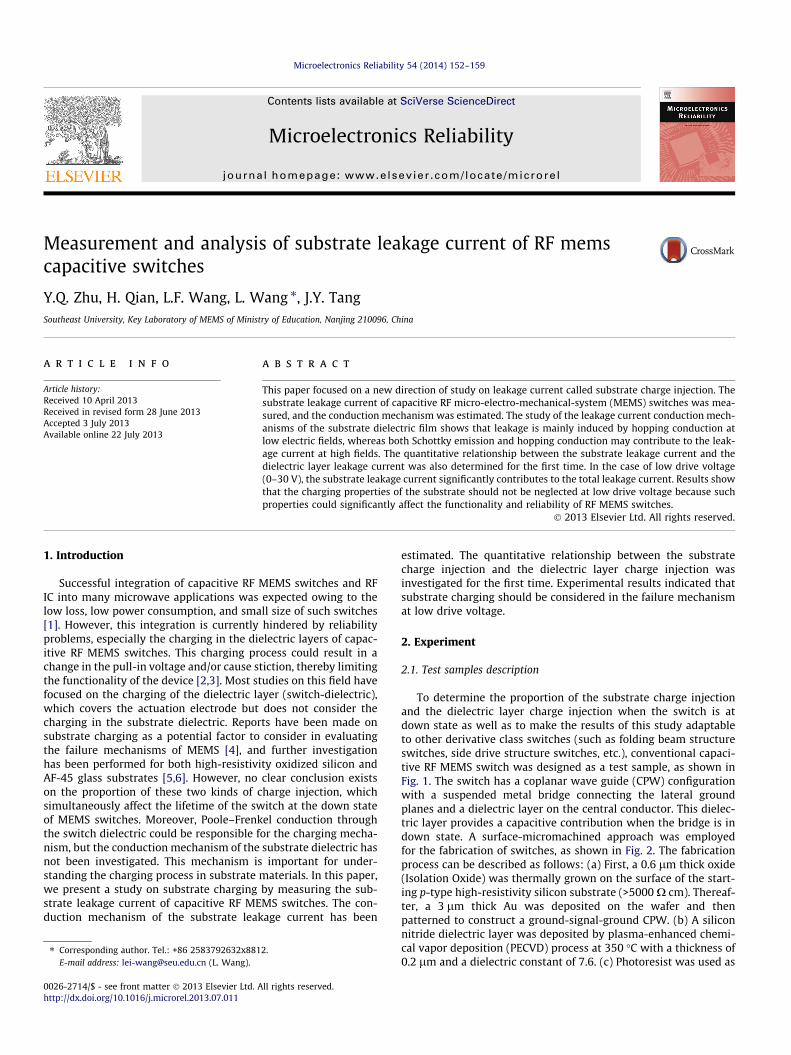
To determine the proportion of the substrate charge injectionand the dielectric layer charge injection when the switch is atdown state as well as to make the results of this study adaptableto other derivative class switches (such as folding beam structureswitches, side drive structure switches, etc.), conventional capaci-tive RF MEMS switch was designed as a test sample, as shown inFig. 1. The switch has a coplanar wave guide (CPW) configurationwith a suspended metal bridge connecting the lateral groundplanes and a dielectric layer on the central conductor. This dielec-tric layer provides a capacitive contribution when the bridge is indown state. A surface-micromachined approach was employedfor the fabrication of switches, as shown in Fig. 2. The fabricationprocess can be described as follows: (a) First, a 0.6 lm thick oxide(Isolation Oxide) was thermally grown on the surface of the start-ing p-type high-resistivity silicon substrate (>5000 X cm). Thereaf-ter, a 3 lm thick Au was deposited on the wafer and thenpatterned to construct a ground-signal-ground CPW. (b) A siliconnitride dielectric layer was deposited by plasma-enhanced chemi-cal vapor deposition (PECVD) process at 350 �C with a thickness of0.2 lm and a dielectric constant of 7.6. (c) Photoresist was used as
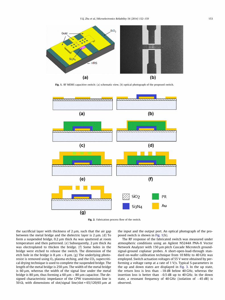
Fig. 1. RF MEMS capacitive switch: (a) schematic view, (b) optical photograph of the proposed switch.
Fig. 2. Fabrication process flow of the switch.
Y.Q. Zhu et al. / Microelectronics Reliability 54 (2014) 152–159 153
the sacrificial layer with thickness of 2 lm, such that the air gapbetween the metal bridge and the dielectric layer is 2 lm. (d) Toform a suspended bridge, 0.2 lm thick Au was sputtered at roomtemperature and then patterned. (e) Subsequently, 2 lm thick Auwas electroplated to thicken the bridge. (f) Some holes in thebridge were etched to release the switch. The dimension of theetch hole in the bridge is 8 lm � 8 lm. (g) The underlying photo-resist is removed using O2 plasma etching, and the CO2 supercriti-cal drying technique is used to complete the suspended bridge. Thelength of the metal bridge is 250 lm. The width of the metal bridgeis 60 lm, whereas the width of the signal line under the metalbridge is 80 lm, thus forming a 60 lm � 80 lm capacitor. The de-signed characteristic impedance of the CPW transmission line is50 X, with dimensions of slot/signal line/slot = 65/120/65 lm at
the input and the output port. An optical photograph of the pro-posed switch is shown in Fig. 1(b).
The RF response of the fabricated switch was measured underatmospheric conditions using an Agilent N5244A PNA-X VectorNetwork Analyzer with 150 lm pitch Cascade Microtech ground-signal-ground coplanar probes. A short-open-load-through stan-dard on-wafer calibration technique from 10 MHz to 40 GHz wasemployed. Switch actuation voltages of 55 V were obtained by per-forming a voltage ramp at a rate of 1 V/s. Typical S-parameters inthe up and down states are displayed in Fig. 3. In the up state,the return loss is less than �18 dB below 40 GHz, whereas theinsertion loss is better than �0.5 dB up to 40 GHz. In the downstate, a resonant frequency of 40 GHz (isolation of �45 dB) isobserved.
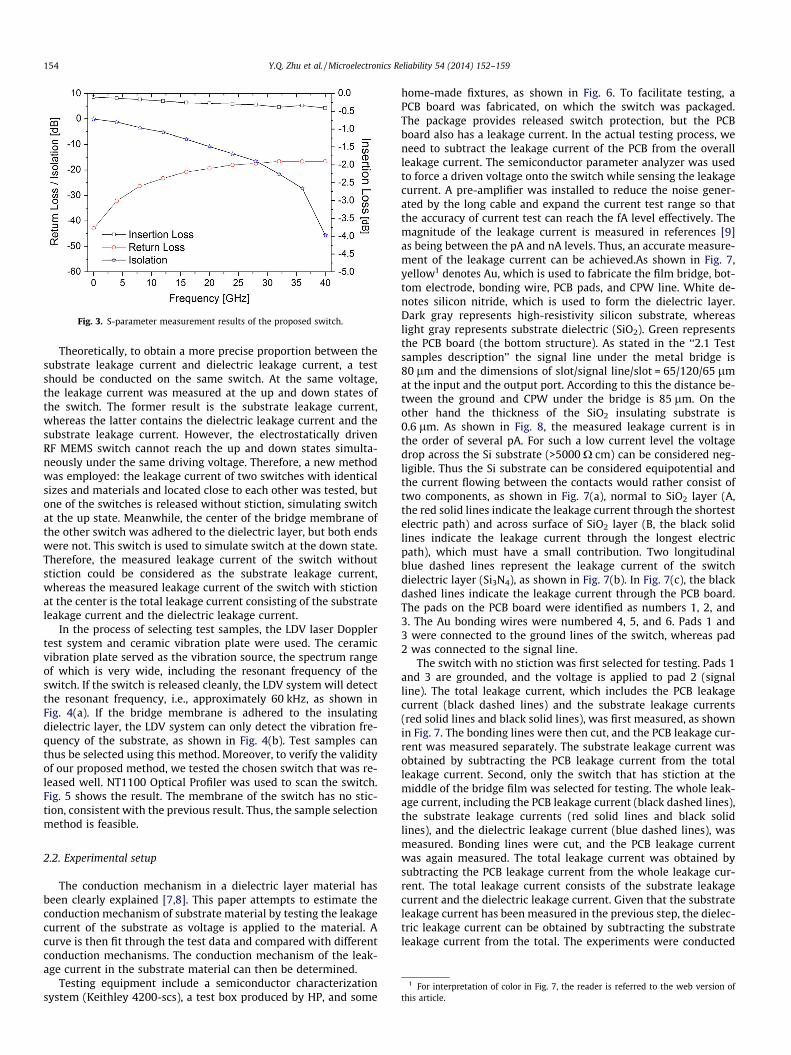
Fig. 3. S-parameter measurement results of the proposed switch.
154 Y.Q. Zhu et al. / Microelectronics Reliability 54 (2014) 152–159
Theoretically, to obtain a more precise proportion between thesubstrate leakage current and dielectric leakage current, a testshould be conducted on the same switch. At the same voltage,the leakage current was measured at the up and down states ofthe switch. The former result is the substrate leakage current,whereas the latter contains the dielectric leakage current and thesubstrate leakage current. However, the electrostatically drivenRF MEMS switch cannot reach the up and down states simulta-neously under the same driving voltage. Therefore, a new methodwas employed: the leakage current of two switches with identicalsizes and materials and located close to each other was tested, butone of the switches is released without stiction, simulating switchat the up state. Meanwhile, the center of the bridge membrane ofthe other switch was adhered to the dielectric layer, but both endswere not. This switch is used to simulate switch at the down state.Therefore, the measured leakage current of the switch withoutstiction could be considered as the substrate leakage current,whereas the measured leakage current of the switch with stictionat the center is the total leakage current consisting of the substrateleakage current and the dielectric leakage current.
In the process of selecting test samples, the LDV laser Dopplertest system and ceramic vibration plate were used. The ceramicvibration plate served as the vibration source, the spectrum rangeof which is very wide, including the resonant frequency of theswitch. If the switch is released cleanly, the LDV system will detectthe resonant frequency, i.e., approximately 60 kHz, as shown inFig. 4(a). If the bridge membrane is adhered to the insulatingdielectric layer, the LDV system can only detect the vibration fre-quency of the substrate, as shown in Fig. 4(b). Test samples canthus be selected using this method. Moreover, to verify the validityof our proposed method, we tested the chosen switch that was re-leased well. NT1100 Optical Profiler was used to scan the switch.Fig. 5 shows the result. The membrane of the switch has no stic-tion, consistent with the previous result. Thus, the sample selectionmethod is feasible.
1 For interpretation of color in Fig. 7, the reader is referred to the web version ofis article.
2.2. Experimental setup
The conduction mechanism in a dielectric layer material hasbeen clearly explained [7,8]. This paper attempts to estimate theconduction mechanism of substrate material by testing the leakagecurrent of the substrate as voltage is applied to the material. Acurve is then fit through the test data and compared with differentconduction mechanisms. The conduction mechanism of the leak-age current in the substrate material can then be determined.
Testing equipment include a semiconductor characterizationsystem (Keithley 4200-scs), a test box produced by HP, and some
home-made fixtures, as shown in Fig. 6. To facilitate testing, aPCB board was fabricated, on which the switch was packaged.The package provides released switch protection, but the PCBboard also has a leakage current. In the actual testing process, weneed to subtract the leakage current of the PCB from the overallleakage current. The semiconductor parameter analyzer was usedto force a driven voltage onto the switch while sensing the leakagecurrent. A pre-amplifier was installed to reduce the noise gener-ated by the long cable and expand the current test range so thatthe accuracy of current test can reach the fA level effectively. Themagnitude of the leakage current is measured in references [9]as being between the pA and nA levels. Thus, an accurate measure-ment of the leakage current can be achieved.As shown in Fig. 7,yellow1 denotes Au, which is used to fabricate the film bridge, bot-tom electrode, bonding wire, PCB pads, and CPW line. White de-notes silicon nitride, which is used to form the dielectric layer.Dark gray represents high-resistivity silicon substrate, whereaslight gray represents substrate dielectric (SiO2). Green representsthe PCB board (the bottom structure). As stated in the ‘‘2.1 Testsamples description’’ the signal line under the metal bridge is80 lm and the dimensions of slot/signal line/slot = 65/120/65 lmat the input and the output port. According to this the distance be-tween the ground and CPW under the bridge is 85 lm. On theother hand the thickness of the SiO2 insulating substrate is0.6 lm. As shown in Fig. 8, the measured leakage current is inthe order of several pA. For such a low current level the voltagedrop across the Si substrate (>5000 X cm) can be considered neg-ligible. Thus the Si substrate can be considered equipotential andthe current flowing between the contacts would rather consist oftwo components, as shown in Fig. 7(a), normal to SiO2 layer (A,the red solid lines indicate the leakage current through the shortestelectric path) and across surface of SiO2 layer (B, the black solidlines indicate the leakage current through the longest electricpath), which must have a small contribution. Two longitudinalblue dashed lines represent the leakage current of the switchdielectric layer (Si3N4), as shown in Fig. 7(b). In Fig. 7(c), the blackdashed lines indicate the leakage current through the PCB board.The pads on the PCB board were identified as numbers 1, 2, and3. The Au bonding wires were numbered 4, 5, and 6. Pads 1 and3 were connected to the ground lines of the switch, whereas pad2 was connected to the signal line.
The switch with no stiction was first selected for testing. Pads 1and 3 are grounded, and the voltage is applied to pad 2 (signalline). The total leakage current, which includes the PCB leakagecurrent (black dashed lines) and the substrate leakage currents(red solid lines and black solid lines), was first measured, as shownin Fig. 7. The bonding lines were then cut, and the PCB leakage cur-rent was measured separately. The substrate leakage current wasobtained by subtracting the PCB leakage current from the totalleakage current. Second, only the switch that has stiction at themiddle of the bridge film was selected for testing. The whole leak-age current, including the PCB leakage current (black dashed lines),the substrate leakage currents (red solid lines and black solidlines), and the dielectric leakage current (blue dashed lines), wasmeasured. Bonding lines were cut, and the PCB leakage currentwas again measured. The total leakage current was obtained bysubtracting the PCB leakage current from the whole leakage cur-rent. The total leakage current consists of the substrate leakagecurrent and the dielectric leakage current. Given that the substrateleakage current has been measured in the previous step, the dielec-tric leakage current can be obtained by subtracting the substrateleakage current from the total. The experiments were conducted
th
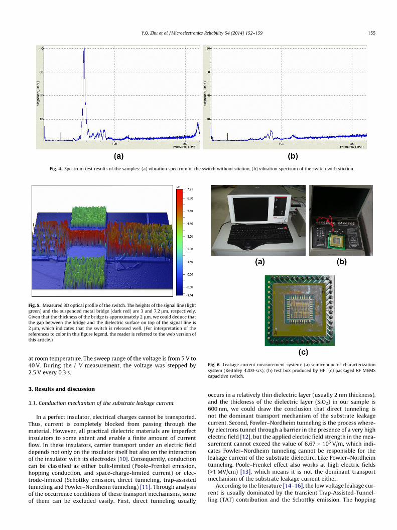
Fig. 5. Measured 3D optical profile of the switch. The heights of the signal line (lightgreen) and the suspended metal bridge (dark red) are 3 and 7.2 lm, respectively.Given that the thickness of the bridge is approximately 2 lm, we could deduce thatthe gap between the bridge and the dielectric surface on top of the signal line is2 lm, which indicates that the switch is released well. (For interpretation of thereferences to color in this figure legend, the reader is referred to the web version ofthis article.)
Fig. 6. Leakage current measurement system: (a) semiconductor characterizationsystem (Keithley 4200-scs); (b) test box produced by HP; (c) packaged RF MEMScapacitive switch.
Fig. 4. Spectrum test results of the samples: (a) vibration spectrum of the switch without stiction, (b) vibration spectrum of the switch with stiction.
Y.Q. Zhu et al. / Microelectronics Reliability 54 (2014) 152–159 155
at room temperature. The sweep range of the voltage is from 5 V to40 V. During the I–V measurement, the voltage was stepped by2.5 V every 0.3 s.
3. Results and discussion
3.1. Conduction mechanism of the substrate leakage current
In a perfect insulator, electrical charges cannot be transported.Thus, current is completely blocked from passing through thematerial. However, all practical dielectric materials are imperfectinsulators to some extent and enable a finite amount of currentflow. In these insulators, carrier transport under an electric fielddepends not only on the insulator itself but also on the interactionof the insulator with its electrodes [10]. Consequently, conductioncan be classified as either bulk-limited (Poole–Frenkel emission,hopping conduction, and space-charge-limited current) or elec-trode-limited (Schottky emission, direct tunneling, trap-assistedtunneling and Fowler–Nordheim tunneling) [11]. Through analysisof the occurrence conditions of these transport mechanisms, someof them can be excluded easily. First, direct tunneling usually
occurs in a relatively thin dielectric layer (usually 2 nm thickness),and the thickness of the dielectric layer (SiO2) in our sample is600 nm, we could draw the conclusion that direct tunneling isnot the dominant transport mechanism of the substrate leakagecurrent. Second, Fowler–Nordheim tunneling is the process where-by electrons tunnel through a barrier in the presence of a very highelectric field [12], but the applied electric field strength in the mea-surement cannot exceed the value of 6.67 � 105 V/m, which indi-cates Fowler–Nordheim tunneling cannot be responsible for theleakage current of the substrate dielectirc. Like Fowler–Nordheimtunneling, Poole–Frenkel effect also works at high electric fields(>1 MV/cm) [13], which means it is not the dominant transportmechanism of the substrate leakage current either.
According to the literature [14–16], the low voltage leakage cur-rent is usually dominated by the transient Trap-Assisted-Tunnel-ling (TAT) contribution and the Schottky emission. The hopping
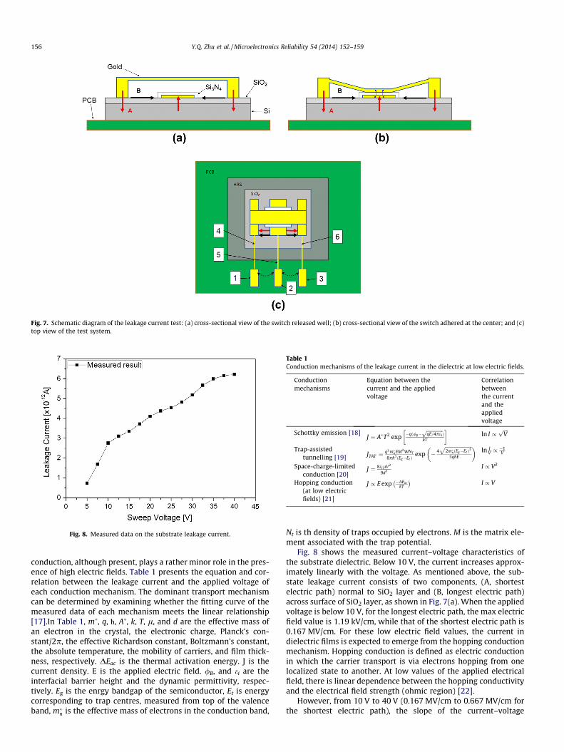
Fig. 7. Schematic diagram of the leakage current test: (a) cross-sectional view of the switch released well; (b) cross-sectional view of the switch adhered at the center; and (c)top view of the test system.
Fig. 8. Measured data on the substrate leakage current.
Table 1Conduction mechanisms of the leakage current in the dielectric at low electric fields.
Conductionmechanisms
Equation between thecurrent and the appliedvoltage
Correlationbetweenthe currentand theappliedvoltage
Schottky emission [18]J ¼ A�T2 exp �qð/B�
ffiffiffiffiffiffiffiffiffiffiffiffiffiqE=4pei
pÞ
kT
� �ln I /
ffiffiffiffiVp
Trap-assistedtunnelling [19] JTAT ¼
q3 m�n EM2 WNT
8p�h3ðEg�Et Þexp � 4
ffiffiffiffiffiffiffiffiffiffiffiffiffiffiffiffiffiffiffiffiffi2m�nðEg�Et Þ3
p3q�hE
� �ln I
V / �1V
Space-charge-limitedconduction [20]
J ¼ 8eilV2
9d3I / V2
Hopping conduction(at low electricfields) [21]
J / E exp �DEackT
� �I / V
156 Y.Q. Zhu et al. / Microelectronics Reliability 54 (2014) 152–159
conduction, although present, plays a rather minor role in the pres-ence of high electric fields. Table 1 presents the equation and cor-relation between the leakage current and the applied voltage ofeach conduction mechanism. The dominant transport mechanismcan be determined by examining whether the fitting curve of themeasured data of each mechanism meets the linear relationship[17].In Table 1, m�, q, ⁄, A�, k, T, l, and d are the effective mass ofan electron in the crystal, the electronic charge, Planck’s con-stant/2p, the effective Richardson constant, Boltzmann’s constant,the absolute temperature, the mobility of carriers, and film thick-ness, respectively. DEac is the thermal activation energy. J is thecurrent density. E is the applied electric field. /B, and ei are theinterfacial barrier height and the dynamic permittivity, respec-tively. Eg is the enrgy bandgap of the semiconductor, Et is energycorresponding to trap centres, measured from top of the valenceband, m�n is the effective mass of electrons in the conduction band,
Nt is th density of traps occupied by electrons. M is the matrix ele-ment associated with the trap potential.
Fig. 8 shows the measured current–voltage characteristics ofthe substrate dielectric. Below 10 V, the current increases approx-imately linearly with the voltage. As mentioned above, the sub-state leakage current consists of two components, (A, shortestelectric path) normal to SiO2 layer and (B, longest electric path)across surface of SiO2 layer, as shown in Fig. 7(a). When the appliedvoltage is below 10 V, for the longest electric path, the max electricfield value is 1.19 kV/cm, while that of the shortest electric path is0.167 MV/cm. For these low electric field values, the current indielectric films is expected to emerge from the hopping conductionmechanism. Hopping conduction is defined as electric conductionin which the carrier transport is via electrons hopping from onelocalized state to another. At low values of the applied electricalfield, there is linear dependence between the hopping conductivityand the electrical field strength (ohmic region) [22].
However, from 10 V to 40 V (0.167 MV/cm to 0.667 MV/cm forthe shortest electric path), the slope of the current–voltage
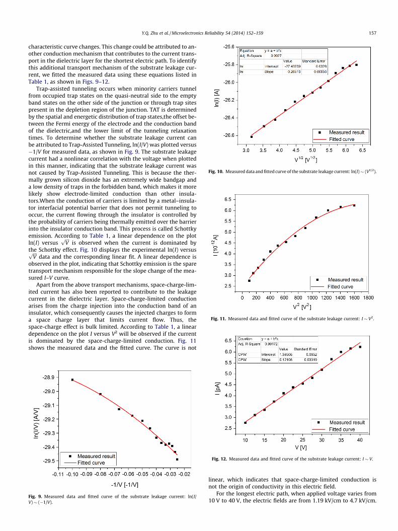
Fig. 10. Measured data and fitted curve of the substrate leakage current: ln(I) � (V1/2).
Fig. 11. Measured data and fitted curve of the substrate leakage current: I � V2.
Y.Q. Zhu et al. / Microelectronics Reliability 54 (2014) 152–159 157
characteristic curve changes. This change could be attributed to an-other conduction mechanism that contributes to the current trans-port in the dielectric layer for the shortest electric path. To identifythis additional transport mechanism of the substrate leakage cur-rent, we fitted the measured data using these equations listed inTable 1, as shown in Figs. 9–12.
Trap-assisted tunneling occurs when minority carriers tunnelfrom occupied trap states on the quasi-neutral side to the emptyband states on the other side of the junction or through trap sitespresent in the depletion region of the junction. TAT is determinedby the spatial and energetic distribution of trap states,the offset be-tween the Fermi energy of the electrode and the conduction bandof the dielectric,and the lower limit of the tunneling relaxationtimes. To determine whether the substrate leakage current canbe attributed to Trap-Assisted Tunneling, ln(I/V) was plotted versus�1/V for measured data, as shown in Fig. 9. The substrate leakagecurrent had a nonlinear correlation with the voltage when plottedin this manner, indicating that the substrate leakage current wasnot caused by Trap-Assisted Tunneling. This is because the ther-mally grown silicon dioxide has an extremely wide bandgap anda low density of traps in the forbidden band, which makes it morelikely show electrode-limited conduction than other insula-tors.When the conduction of carriers is limited by a metal–insula-tor interfacial potential barrier that does not permit tunneling tooccur, the current flowing through the insulator is controlled bythe probability of carriers being thermally emitted over the barrierinto the insulator conduction band. This process is called Schottkyemission. According to Table 1, a linear dependence on the plotln(I) versus
ffiffiffiffiVp
is observed when the current is dominated bythe Schottky effect. Fig. 10 displays the experimental ln(I) versusffiffiffiffi
Vp
data and the corresponding linear fit. A linear dependence isobserved in the plot, indicating that Schottky emission is the sparetransport mechanism responsible for the slope change of the mea-sured I–V curve.
Apart from the above transport mechanisms, space-charge-lim-ited current has also been reported to contribute to the leakagecurrent in the dielectric layer. Space-charge-limited conductionarises from the charge injection into the conduction band of aninsulator, which consequently causes the injected charges to forma space charge layer that limits current flow. Thus, thespace-charge effect is bulk limited. According to Table 1, a lineardependence on the plot I versus V2 will be observed if the currentis dominated by the space-charge-limited conduction. Fig. 11shows the measured data and the fitted curve. The curve is not
Fig. 9. Measured data and fitted curve of the substrate leakage current: ln(I/V) � (�1/V).
Fig. 12. Measured data and fitted curve of the substrate leakage current: I � V.
linear, which indicates that space-charge-limited conduction isnot the origin of conductivity in this electric field.
For the longest electric path, when applied voltage varies from10 V to 40 V, the electric fields are from 1.19 kV/cm to 4.7 kV/cm.
158 Y.Q. Zhu et al. / Microelectronics Reliability 54 (2014) 152–159
In this field range, the occurrence condition of hopping conductioncan still be met. The fitting result also shows that the hopping con-duction mechanism still contributes to the charge carrier transportin this voltage range, as show in Fig. 12.
Based on the above discussion, we could estimate that for lowapplied voltage (<10 V), the mechanism of the substrate leakagecurrent was estimated as hopping conduction, whereas for appliedvoltage ranging from 10 to 40 V, Schottky emission becomes thedominant conduction mechanism rather than the Frenkel–Pooleemission mechanism. Meanwhile, the hopping conduction mecha-nism still contributes to the charge carrier transport in this voltagerange. This is a transitional behavior between Ohmic and blockingcontacts. Thus, the conduction of carriers depends on bothcontributions.
Fig. 14. Proportion of substrate leakage current to the total leakage current vs. biasvoltage.
3.2. Correlation between substrate leakage current and total leakagecurrent
Fig. 13 shows the magnitude of the leakage current is approxi-mately 10�11 A, consistent with previously reported results. In thecase of low voltage (0–30 V), substrate leakage current signifi-cantly contributes to the total leakage current, but this contribu-tion decreases rapidly at voltages above 30 V. Compared with thedielectric leakage current, the contribution of the substrate leakagecurrent could be ignored (<15%) at voltages above 40 V, as shownin Fig. 14. The proportion of the substrate leakage current to the to-tal leakage current can be expected to be further reduced as thevoltage increases.
This result could be explained by the difference in the conduc-tion mechanism between the substrate leakage current and thedielectric leakage current. Electrical conduction in silicon nitridedielectrics has been studied by many researchers. In this dielectric,the conduction mechanism was observed to be Ohmic conductionat low fields, while Poole–Frenkel emission was proposed for highfields [23,24]. In this paper, we revealed that only hopping conduc-tion occurs at low fields in the substrate dielectric, whereas bothSchottky emission and hopping conduction may contribute to theleakage current at high fields. Thus, at high electric fields, the rela-tionship between the substrate leakage current and the appliedvoltage is between linear and exponential, whereas the relation-ship between the dielectric leakage current and the applied voltageis exponential. Therefore, the dielectric leakage current grows fas-ter than the substrate leakage current when applied voltage in-creases. The proportion of the substrate leakage current to thetotal leakage current will become increasingly smaller.
Fig. 13. Measured results of substrate leakage current and total leakage current.
Substrate leakage current can affect capacitive RF MEMSswitches in two aspects. First is in terms of the power loss of theswitch. Dielectric leakage causes power loss when the switch isoperating, given that current flows from the signal line to theground when the high-power signal passes through the switch.Second is in terms of the reliability of the switch. The substrateleakage current could induce charges trapped in the substratedielectric, which can affect the distribution of the electrostaticforce, change the pull-in voltage of the switch, and may even causestiction, thus limiting the functionality of the device [4,5].
The above results are significant in switch design, especially forswitches with relatively small pull-in voltage (less than 30 V), con-sidering that substrate leakage current should not be ignored inthese devices. Designers need to consider the electrical character-istics of the substrate materials.
4. Conclusions
This paper aims to obtain better insight into the dielectriccharging mechanisms of the substrate dielectric by measuringthe substrate leakage current of RF MEMS capacitive switches.We revealed that in the substrate dielectric, hopping conductionoccurs at low fields, whereas both Schottky emission and hoppingconduction may contribute to the leakage current at high fields.Moreover, the experiment results indicate that substrate leakagecurrent has obvious contribution on the total leakage current inthe case of low voltage (0–30 V). For switches with relatively smallpull-in voltage (less than 30 V), the charging properties of the sub-strate should not be ignored as these properties may affect thefunctionality and reliability of RF MEMS switches.
Acknowledgment
The work is supported by the National Natural Science Founda-tion of China (61106114).
References
[1] Rebeiz GM, Muldavin JB. RF MEMS switches and switch circuits. MicrowaveMag, IEEE 2001;2(4):59–71.
[2] Goldsmith C, Ehmke J, Malczewski A, et al. Lifetime characterization ofcapacitive RF MEMS switches. Microwave symposium digest, 2001 IEEE MTT-Sinternational. IEEE 2001, vol. 1. p. 227-30.
[3] Yuan X, Cherepko SV, Hwang JCM, et al. Initial observation and analysis ofdielectric-charging effects on RF MEMS capacitive switches. IEEE MTT-Sinternational microwave symposium 2001. p. 1943–6.
Y.Q. Zhu et al. / Microelectronics Reliability 54 (2014) 152–159 159
[4] Czarnecki P, Rottenberg X, Soussan P, et al. Effect of substrate charging on thereliability of capacitive RF MEMS switches. Sens Actuat A: Phys2009;154(2):261–8.
[5] Czarnecki P, Rottenberg X, Soussan P, et al. Influence of the substrate on thelifetime of capacitive RF MEMS switches. In: Digest, proceedings of the 21stIEEE MEMS2008 techn., Tucson, AZ, USA, January 13–17; 2008. p. 172–5.
[6] Mardivirin D, Pothier A, El Khatiob M, et al. Charging in dielectricless capacitiveRF MEM- S switches. IEEE Trans Microwave Theory Tech 2009;57(1):231–6.
[7] Koszewski Adam, Souchon Frederic, Thierry Ouisse. Conduction and trappingin RF MEMS capacitive switches with a SiN layer. In: Proceedings of theEuropean IEEE. Solid state device research conference, 2009. ESSDERC’09;2009. p. 339–42.
[8] Zaghloul U, Papaioannou G, Coccetti F, et al. Dielectric charging in siliconnitride films for MEMS capacitive switches: effect of film thickness anddeposition conditions. Microelectr Reliab 2009;49(9):1309–14.
[9] Yuan X, Hwang JCM, Forehand D, Goldsmith CL. Modeling and characterizationof dielectric charging effects in RF MEMS capacitive switches. in 2005 IEEEMTT-S; 2005. p. 753–756.
[10] McGill TC, Kurtin S, Fishbone L, et al. Contact-limited currents in metal-insulator-metal structures. J Appl Phys 1970;41(9):3831–9.
[11] Simmons JG. Conduction in thin dielectric films. J Phys D: Appl Phys1971;4(5):613.
[12] Bose M, Basa DK, Bose DN. Electrical conduction studies of plasma enhancedchemical vapor deposited silicon nitride films. J Vac Sci Technol A: Vac SurfFilms 2001;19(1):41–4.
[13] Lenzlinger M, Snow EH. Fowler-nordheim tunneling into thermally grownSiO2. J Appl Phys 1969;40(1):278–83.
[14] Ramprasad R. Phenomenological theory to model leakage currents in metal–insulator–metal capacitor systems. Phys Status Solidi B 2003;239(1):59–70.
[15] Koutsoureli M, Michalas L, Papaioannou G. Temperature effects on the bulkdischarge current of dielectric films of MEMS capacitive switches. MicroelectrReliab 2012;52(9–10):2240–4.
[16] Koutsoureli M, Michalas L, Papaioannou G. Charge collection mechanism inMEMS capacitive switches. Reliability physics symposium (IRPS), 2012 IEEEinternational. IEEE; 2012. p. ME.2.1–ME.2.5.
[17] Wang Chenggang et al. Characteristics of leakage current mechanisms andSILC effects of HfO2 gate dielectric. Chin J Semicond 2004;25(7):841–1.
[18] Emtage PR, Tantraporn W. Schottky emission through thin insulating films.Phys Rev Lett 1962;8(7):267–8.
[19] Gopal V, Singh SK, Mehra RM. Analysis of dark current contributions inmercury cadmium telluride junction diodes. Infrared Phys Technol2002;43(6):317–26.
[20] Many A, Rakavy G. Theory of transient space-charge-limited currents in solidsin the presence of trapping. Phys Rev 1962;126(6):1980.
[21] Attaf A, Benkhedir ML, Aida MS. Influence of substrate bombardment onsputtered a-Si: N thin film properties. Phys B: Conden Matter2005;355(1):270–9.
[22] Govor LV, Bashmakov IA, Boehme K, et al. Electrical field dependence ofhopping conduction in self-organized carbon networks. J Appl Phys2002;91(2):739–47.
[23] Sze SM. Current transport and maximum dielectric strength of silicon nitridefilms. J Appl Phys 1967;38(7):2951–6.
[24] Shannon JM, Deane SC, McGarvey B, et al. Current induced drift mechanism inamorphous SiNx: H thin film diodes. Appl Phys Lett 1994;65(23):2978–80.