reliability evaluation
TRANSCRIPT
76
S C I E N C E & T E C H N O L O G Y T R E N D S
Introduction
1-1 Discovery of Graphene; Potentiality of Breaking through the Limitations of Semiconductors
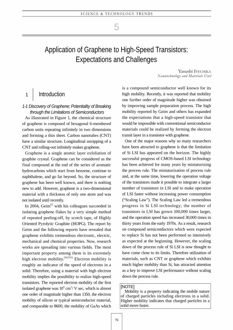
As illustrated in Figure 1, the chemical structure of graphene is composed of hexagonal 6-membered carbon units repeating infinitely in two dimensions and forming a thin sheet. Carbon nanotubes (CNT) have a similar structure. Longitudinal unzipping of a CNT and rolling-out infi nitely makes graphene. Graphene is a single atomic layer exfoliation of graphite crystal. Graphene can be considered as the final compound at the end of the series of aromatic hydrocarbons which start from benzene, continue to naphthalene, and go far beyond. So, the structure of graphene has been well known, and there is nothing new to add. However, graphene is a two-dimensional material with a thickness of only one atom and was not isolated until recently. In 2004, Geim[1] with his colleagues succeeded in isolating graphene flakes by a very simple method of repeated peeling-off, by scotch tape, of Highly Oriented Pyrolytic Graphite (HOPG). The report by Geim and the following reports have revealed that graphene exhibits tremendous electronic, electric, mechanical and chemical properties. Now, research works are spreading into various fields. The most important property among them is its extremely high electron mobility.[NOTE] Electron mobility is roughly an indicator of the speed of electrons in a solid. Therefore, using a material with high electron mobility implies the possibility to realize high-speed transistors. The reported electron mobility of the fi rst isolated graphene was 104 cm2/ V sec, which is almost one order of magnitude higher than 1350, the electron mobility of silicon or typical semiconductor material, and comparable to 8600, the mobility of GaAs which
5
Application of Graphene to High-Speed Transistors: Expectations and Challenges
Yasushi IYECHIKANanotechnology and Materials Unit
1is a compound semiconductor well known for its high mobility. Recently, it was reported that mobility one further order of magnitude higher was obtained by improving sample preparation process. The high mobility reported by Geim and others has expanded the expectations that a high-speed transistor that would be impossible with conventional semiconductor materials could be realized by forming the electron transit layer in a transistor with graphene. One of the major reasons why so many researchers have been attracted to graphene is that the limitation of Si LSI has appeared on the horizon. The highly successful progress of CMOS-based LSI technology has been achieved for many years by miniaturizing the process rule. The miniaturization of process rule and, at the same time, lowering the operation voltage of the transistors made it possible to integrate a larger number of transistors in LSI and to make operation of LSI faster without increasing power consumption (“Scaling Law”). The Scaling Law led a tremendous progress in Si LSI technology; the number of transistors in LSI has grown 100,000 times larger, and the operation speed has increased 30,000 times in thirty years from the early 1970s. As a result, research on compound semiconductors which were expected to replace Si has not been performed so intensively as expected at the beginning. However, the scaling down of the process rule of Si LSI is now thought to have come close to its limits. Therefore utilization of materials, such as CNT or graphene which exhibits much higher mobility than Si, has attracted attention as a key to improve LSI performance without scaling down the process rule.
[NOTE] Mobility is a property indicating the mobile nature of charged particles including electrons in a solid. Higher mobility indicates that charged particles in a solid move faster.
Q U A R T E R L Y R E V I E W N o . 3 7 / O c t o b e r 2 0 1 0
77
Taking into account such trends, the International Technology Roadmap for Semiconductors (ITRS) committee has added carbon materials including CNT and graphene to the list of promising materials or technologies for future high-performance LSI, and has been discussing the feasibility. On the other hand, at a meeting held in 2009, the discussion was made under an assumption that the realization of graphene-based technologies would not come before 2019.[2] The meaning of this is that it will require a long time of research and development for the realization of graphene-based devices because, in spite of its wonderful potentiality, the research and development of graphene are still at an early and basic stage and there are still a number of technical challenges. For example, although some methods for graphene formation have been proposed, exfoliation of HOPG by scotch tape, the fi rst method used for the formation of graphene, is still used in many reports on graphene-based transistors. This suggests that a practical method of forming high quality graphene has not yet been developed. In this report, the following subjects concerning graphene will be focused on : general properties of graphene, widely-used graphene formation technologies, research on graphene-based transistors, and challenges for realization of graphene-based high-speed transistors.
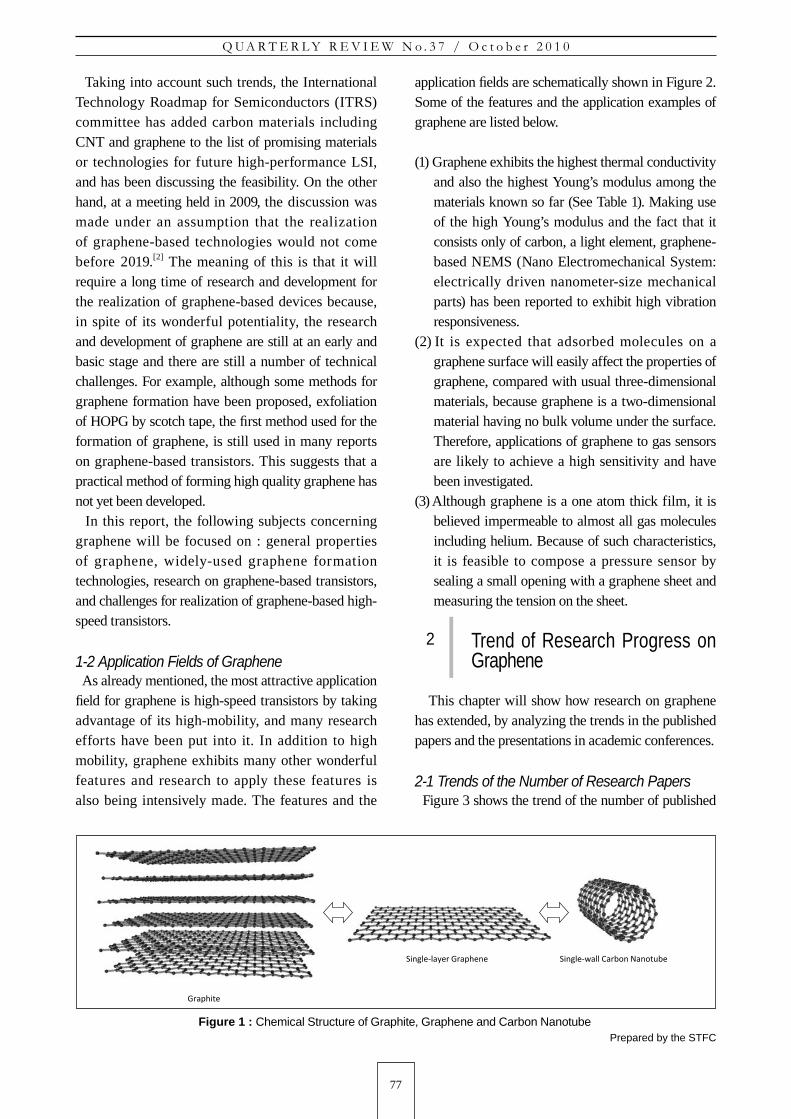
1-2 Application Fields of Graphene As already mentioned, the most attractive application fi eld for graphene is high-speed transistors by taking advantage of its high-mobility, and many research efforts have been put into it. In addition to high mobility, graphene exhibits many other wonderful features and research to apply these features is also being intensively made. The features and the
application fi elds are schematically shown in Figure 2. Some of the features and the application examples of graphene are listed below.
(1) Graphene exhibits the highest thermal conductivity and also the highest Young’s modulus among the materials known so far (See Table 1). Making use of the high Young’s modulus and the fact that it consists only of carbon, a light element, graphene-based NEMS (Nano Electromechanical System: electrically driven nanometer-size mechanical parts) has been reported to exhibit high vibration responsiveness.
(2) It is expected that adsorbed molecules on a graphene surface will easily affect the properties of graphene, compared with usual three-dimensional materials, because graphene is a two-dimensional material having no bulk volume under the surface. Therefore, applications of graphene to gas sensors are likely to achieve a high sensitivity and have been investigated.
(3) Although graphene is a one atom thick film, it is believed impermeable to almost all gas molecules including helium. Because of such characteristics, it is feasible to compose a pressure sensor by sealing a small opening with a graphene sheet and measuring the tension on the sheet.
Trend of Research Progress on Graphene
This chapter will show how research on graphene has extended, by analyzing the trends in the published papers and the presentations in academic conferences.
2-1 Trends of the Number of Research Papers Figure 3 shows the trend of the number of published
Graphite
Single-layer Graphene Single-wall Carbon Nanotube
Figure 1 : Chemical Structure of Graphite, Graphene and Carbon NanotubePrepared by the STFC
2
78
S C I E N C E & T E C H N O L O G Y T R E N D S
papers on graphene with regard to calendar year. They were retrieved out of the ISI Web of Knowledge database. The retrieval of papers was performed using the keywords “graphene” for the topic and “article” for the media. It is clearly shown in this figure that the number of papers has rapidly increased since the isolation of graphene was reported for the first time in 2004. In 2009, approximately 1,800 papers were published which is over 10 times larger than the number of papers in 2004. Before 2004, almost all of the retrieved papers were about CNT, and some were devoted to theoretical study of graphene. Although some of the recent papers are on the performance of graphene-based devices, the majority of the papers are on the basic properties of graphene. This suggests that research on graphene is still at the early and basic stage. Figure 4 shows a trend analogous to Figure 3 by countries. The top 8 countries are taken in this fi gure, based on the number of papers from each country in 2009. The numbers of papers in 2009 are approximately 10 times as large as in 2005 for almost of all of these 8 countries. In the case of the US, the top in 2009, the number of
papers is twice as large as the second country, and its increasing rate seems to be close to the world average, if we compare the trend with that of the world total shown in Figure 3. It is China and Korea that showed the highest increasing rate from 2005 to 2009. The rate is about 20 in the case of China. In the case of Korea, the number of papers was almost zero in 2005, but it was as large as 70 in 2009. Although Japan was second in 2005, and the number of papers from Japan in 2009 is 5 times as large as in 2004, it fell back to fourth in 2009. Similar analysis was made for research institutions. Figure 5 summarizes the trend for 8 institutions which are the top 8 in 2009. The most distinctive institution in 2009 is the Chinese Academy of Science. The number of papers from the academy is almost 30% of all of the papers from Chinese institutions. It means that in China, submission of papers is concentrated in a limited number of institutions. On the other hand, in the US, although a large number of papers are submitted as a total, diverse institutions contribute to it.
Prepared by the STFC based on the References[3–8]
Figure 2 : Distinctive Properties of Graphene and Possible Application Fields
MaterialThermal Conductivity Young’s Modulus
W/cm・K 109Pa (GPa)
Graphene ~ 50 1500
Carbon Nanotube ~ 35 ~ 1000
Diamond 10 ~ 22 1050 ~ 1200
Si 1.4 131
Ge 0.6 103
SiC 4.1 450
Table 1 : Thermal Conductivity and Young’s Modulus of Graphene and Typical Semiconductor Materials
Prepared by the STFC based on Reference[3]
������������� ���
�����������
��������
����������������� �������
������������������ �
�������� �������� ����� �
��� ���������������� �
������������������ ������
!������������
"������������
�����������
����� ���
#���������� ���
���� ����� ����
�������
���������� ��������
���������������
������������������
������������������
���������� ��������
�������������������
�������������������
� �!���� ����
"��������
����!��������#��
�������!�� ���

Q U A R T E R L Y R E V I E W N o . 3 7 / O c t o b e r 2 0 1 0
79
Prepared by the STFC
Figure 3 : Yearly Trends of Papers Regarding Graphene
2009
2005
Num
ber o
f Pap
ers
USA
China
Germany Japan
France UK Spain Korea
Prepared by the STFCFigure 4 : Yearly Trends of Papers by Countries
Prepared by the STFC
Figure 5 : Yearly Trends of Papers by Research Institutions
�������
����
�
�
�
�
�
�
�
���������� ���
����������� �����
�����
���������
��������������
��������� ���������
������������������
��� �����
������
�������
����������
��������
����
����
�������
����
�
�
�
�
�
�
�
���������� ���
����������� �����
�����
���������
��������������
��������� ���������
������������������
��� �����
������
�������
����������
��������
����
����
CNRS: Centre National de la Recherche Scientifi que (French National Center for Scientifi c Research), CSIC: Consejo Superior de Investigaciones Científi cas (Spanish National Research Council), UCB: University of California, Berkley
�
���
����
����
����
���� ���� ���� ���� ����
����������
���������������� ����
���� �����������
���������� ���
����
80
S C I E N C E & T E C H N O L O G Y T R E N D S
2-2 Comparison between Conferences in US and in Japan on Graphene
Comparison between the numbers of presentations in recent academic conferences held in Japan and in the US will be made here. They are the 57th Spring Meeting of the Japan Society of Applied Physics held in March 2010 (hereinafter referred to as “JSAP”) and the Fall Meeting of Materials Research Society held from November through December 2009 (hereinafter referred to as “MRS”). Both of them are general conferences, covering various fields, and are held twice annually, in spring and fall. Figure 6 summarizes the trends of the presentations at the conferences. In JSAP, the presentations on materials including CNT and graphene were performed at “Session Nanocarbon.” The number of the presentations in this session was 155. After classifying each presentation by its title into one of the categories, CNT, graphene, and others, 74 were on CNT, and 58 on graphene. That is, 132 presentations were on CNT and graphene. Almost all of the 58 presentations on graphene were from universities and public institutions. As for the presentations made by a private company (or companies) without collaborating with universities or public institutions, 5 were from
NTT Corporation and 1 from Fujitsu Laboratories Ltd. Most of the presentations on graphene were on evaluation of basic material properties. MRS had a session, “large-area electronics from CNT, Graphene and other materials.” There were 120 presentations made, nearly the same as that of JSAP. Out of them, 40 were on CNT and 80 were on graphene. Many more presentations were made on graphene than on CNT. This trend differs from JSAP. In the presentations made by US organizations or by collaboration with US organizations, 56 were on graphene, whereas 23 were on CNT. This ratio of graphene to CNT is slightly larger than that of the total of MRS. On the other hand, out of the presentations on graphene, 6 were on application to electronic devices, suggesting that, in the US as well as in Japan, most research activities are still confi ned around the basic area. Also, only 6 presentations on graphene were from private companies without collaborating with universities or public institutions, and public institutions and universities made most of the presentations. This trend is also seen in JSAP. It can be concluded from the above analysis that the research activities on graphene are still at the early and basic stage, and are led by universities
(a) Ratio of the presentations of graphene and CNT
(b) Percentage Analysis of the Presenters
0% 20% 40% 60% 80% 100%
CNT JSAP, March 2010
MRS, Fall 2009
Graphene
MRS, Fall 2009Presentations by US or collaboration with US organization(s)
presentations in JSAP, March 58
Private Corporations, 10%
Co-presented by Private Corporations and Universities or
Public Organizations, 19%
Other than Private Corporations, 71%
2009presentations in MRS, Fall 80
Private Corporations,
Co-presented by Private Corporations and Universities
or Public Organizations, 8%
Other than Private Corporations, 84%
Other than Private Corporations, 71%
Other than Private Corporations, 84%
Prepared by the STFCFigure 6 : Trends in the Presentations in Academic Conferences in US and Japan

Q U A R T E R L Y R E V I E W N o . 3 7 / O c t o b e r 2 0 1 0
81
or public institutions both in the US and in Japan. Concerning the applications for high-speed electronic devices taking advantage of the excellent properties of graphene, although there were not so many presentations, some of them are notable. Especially presentations by IBM seem to overwhelm the rest.
Electronic Properties of Graphene
This chapter will be devoted mainly to the introduction of the electronic properties of graphene, which is the key factor for the application to electronics. In addition, a brief comparison between graphene and CNT, which is also expected to be applied to electronics, will be made.
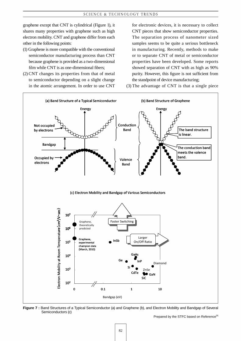
3-1 Electronic Properties Figure 7 illustrates the band structure of graphene (b) in comparison with that of a typical semiconductor (a). An electron propagates as a wave in a crystal. A band structure illustrates the relation of the wave number to the energy of electrons in a crystal. Electrons in a crystal successively occupy from the lower states to the upper in the band structure (from the lower part to the upper part in the fi gures). As is shown in Figure 7 (a), the band structures of a typical semiconductor splits into two bands, the upper and the lower. Usually, there are almost no electrons in the upper band, and there are almost no vacancies of electrons (holes) in the lower band. The upper and the lower bands are called the conduction band and the valence band, respectively. Between the conduction band and the valence band, there exists an energy zone where there are no states for electrons to occupy, which is called a bandgap. In Figure 7 (c), the bandgap and electron mobility at room temperature for several semiconductors are summarized. The band structure of graphene differs from that of a typical semiconductor in the following points:
(1) at around the point where the conduction band and the valence band meet each other, the slope of the band structure is linear ;
(2) the conduction band is connected continuously with the valence band, which means the bandgap is zero.
With respect to characteristic (1) of the band structure, in the case of a typical semiconductor,
the band structure at around the top of the valence band and the bottom of the conduction band shows a parabolic shape and the slope changes gradually. The larger the change of the slope of the band, the less the effective-mass of the electrons (virtual mass of electrons in a material). On the other hand, in the case of graphene, because the slope is linear, the effective mass of electrons is zero. This means that graphene shows very high electron-mobility. A theoretical expectation of the electron-mobility of graphene is 1,000 times higher than that of silicon, and an electron mobility as high as 2×106cm2/V sec[10,11] has been experimentally achieved, which is 100 times higher than that of silicon. Because higher electron mobility leads to shorter switching time for a transistor, graphene has been expected as a material that could realize high-speed electronic devices which could break the speed records made by conventional semiconductors such as silicon or compound semiconductors. For that reason, graphene has been expected to be applied to high speed-transistors. In addition, graphene has been paid much attention as a target of physics because the zero effective mass in graphene is a special quantum mechanical phenomenon.[3,12] On the other hand, the zero bandgap in graphene, mentioned in (2), means that a very small thermal energy excites electrons out of the valence band up to the conduction band. Therefore, graphene cannot be kept semi-insulating. In general, materials should be controlled to have high electric impedance for high signal intensity when applied to digital devices, because digital devices are required to have a high switching on/off ratio. Therefore, the zero bandgap of graphene is a very high hurdle for application to digital transistors. Several methods are proposed to open the bandgap of graphene, and some experiments have been reported to succeed to tune the bandgap, which will be mentioned in 5-1. Generally speaking, the wider bandgap of graphene is achievable by deforming, more or less, the band structure illustrated in Figure 7 (b), and may therefore easily result in diminishing the advantage of high electron mobility. In this respect, it is a big challenge for the technology development of graphene, to make the bandgap wider without diminishing the high electron mobility.
3-2 Comparison with Carbon Nanotube (CNT) Because CNT has the same atomic arrangement as
3
82
S C I E N C E & T E C H N O L O G Y T R E N D S
Prepared by the STFC based on Reference[9]
Figure 7 : Band Structures of a Typical Semiconductor (a) and Graphene (b), and Electron Mobility and Bandgap of Several Semiconductors (c)
graphene except that CNT is cylindrical (Figure 1), it shares many properties with graphene such as high electron mobility. CNT and graphene differ from each other in the following points:(1) Graphene is more compatible with the conventional
semiconductor manufacturing process than CNT because graphene is provided as a two-dimensional fi lm while CNT is as one-dimensional fi bers;
(2) CNT changes its properties from that of metal to semiconductor depending on a slight change in the atomic arrangement. In order to use CNT
for electronic devices, it is necessary to collect CNT pieces that show semiconductor properties. The separation process of nanometer sized samples seems to be quite a serious bottleneck in manufacturing. Recently, methods to make or to separate CNT of metal or semiconductor properties have been developed. Some reports showed separation of CNT with as high as 90% purity. However, this fi gure is not suffi cient from the standpoint of device manufacturing;
(3) The advantage of CNT is that a single piece
������
���� �����
����������
�������
������
��� ��������
�������
��� ����
����
��������
����
����������� � ���
����������
������� ���������
����������������
�����
��������� � � ���!����������� ������ �� ��������� � � ���!�"�������
�����������#������������������!����� �� ������ ���
������
�
������
���
���
���������� �����������
������� �����
���� ����
���������� ���
������
�
������
���
���
���������� �����������
������� �����
���� ����
���������� ���
������
���� �����
����������
�������
������
��� ��������
�������
��� ����
����
��������
����
����������� � ���
����������
������� ���������
����������������
�����
��������� � � ���!����������� ������ �� ��������� � � ���!�"�������
�����������#������������������!����� �� ������ ���
��
���
�
��
����
���
���
���
����
� ��� � ��
����� ��� ����������� ����������������
�
������
���
���
���
���
���
���
���������� ���
�������
���� �!���"
��������
������� �����
���� ����
��������
����� ������
����� ������
�����������
#�����$�%�&'
(��)"��
���������� ���
�������
���� �!���"
��
���
�
��
����
���
���
���
����
� ��� � ��
����� ��� ����������� ����������������
�
������
���
���
���
���
���
���
���������� ���
�������
���� �!���"
��������
������� �����
���� ����
��������
����� ������
����� ������
�����������
#�����$�%�&'
(��)"��
���������� ���
�������
���� �!���"
Q U A R T E R L Y R E V I E W N o . 3 7 / O c t o b e r 2 0 1 0
83
of CNT can be used for the device fabrication directly, whereas graphene should be processed to have semiconducting nature before device fabrication.
Growth and Evaluation Methods of Graphene
4-1 Production Methods Some widely used or important production methods of graphene will be reviewed in this section. Among them, mechanical exfoliation of HOPG and conversion of SiC surface have been reported to be effective for better transistor properties than others. However, no production methods to form large-area uniform graphene suffi cient for the fabrication of devices have been developed so far.
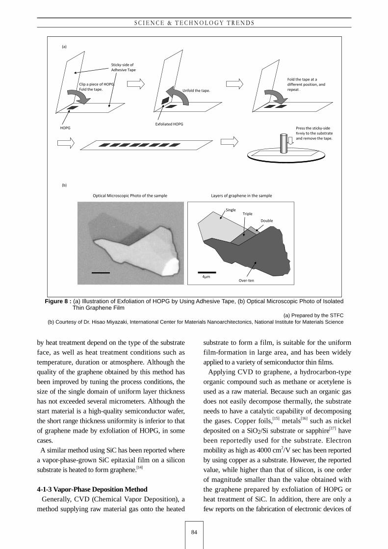
4-1-1 Exfoliation of Highly Oriented Pyrolytic Graphite (HOPG) HOPG, which is generally prepared through high-temperature treatment of organic compounds, has a crystalline structure where graphene layers are stacked. A graphene layer is easily peeled off because there is only weak, van der Waals, force between the layers. By utilizing this property, Geim and his coworkers successfully isolated graphene by repeatedly exfoliating HOPG with scotch tape.[1] The isolated graphene was transferred onto another appropriate substrate fi nally. This process is illustrated in Figure 8 (a). This method is quite simple as easily can be seen in this figure. Some video websites on the Internet provide movies of the process. Figure 8 (b) shows an optical microscopic photo of graphene obtained by this method. Generally, the half-width of X-ray diffraction (X-ray rocking curve) peak of HOPG is around 0.4 degrees, which is roughly two orders of magnitude larger than that of a typical semiconductor. This means that the crystalline quality of HOPG is very low compared with other semiconductor crystals. This low crystallinity seems to indicate that HOPG consists of many small crystals (domains) and that the directions of domains are rather scattered. Therefore, it is not realistic by the exfoliation of HOPG to obtain a graphene fl ake of larger area than the domain size of HOPG. Furthermore, it is not practicable to exfoliate HOPG with a thickness precision of a single atomic
layer. As a result, the obtained continuous sample of graphene consists of various parts of a different number of layers. The optical microscopic observation photo in Figure 8 (b) shows such a situation clearly. Exfoliation is performed manually and in an ordinary atmosphere. So, it would be considered highly possible that impurities and adsorbates on the surface of graphene or mechanical damages will have much infl uence in the sample formed by this method. However, so far, the samples obtained by exfoliation have often shown higher mobility than that of samples obtained by other methods. Because the exfoliation method is simple and convenient and, at the same time, the material properties of obtained samples are relatively good compared with those obtained by other methods, almost all of the reported devices have used graphene obtained by exfoliation. Although the exfoliation method has a drawback in that it is hard to obtain a large-area sample for practical use, it will remain as a sample production method for the proof-of-concept devices. Another method using HOPG, where HOPG is ultrasonicated in organic solvent, has been reported.[3] Because the graphene obtained by this method is suspended in the solvent, a thin graphene film is obtained by applying the graphene containing solvent to a substrate. However, high-quality graphene for device fabrication and evaluation would not be obtained by this method.
4-1-2 Surface Conversion of Silicon Carbide (SiC) by Heat Treatment It is reported that heat treatment of SiC in a vacuum or in an inert atmosphere forms a graphene layer on the SiC surface,[13] which is a result of evaporation of silicon atoms from the SiC surface and of resultant segregation of carbon atoms on the surface. This method has been expected to be suitable for the preparation of high-quality graphene, because high-quality SiC wafers for semiconductor manufacturing are commercially available, and process in a vacuum or in an inert atmosphere diminishes the undesirable infl uence of impurities. However, there have been no reports of high-performance devices by this method until recently. Due to the polarity of SiC crystal, a generally available SiC substrate has two faces, i.e. a silicon face and a carbon face. Properties of graphene obtained
4
84
S C I E N C E & T E C H N O L O G Y T R E N D S
Figure 8 : (a) Illustration of Exfoliation of HOPG by Using Adhesive Tape, (b) Optical Microscopic Photo of Isolated Thin Graphene Film
(a) Prepared by the STFC(b) Courtesy of Dr. Hisao Miyazaki, International Center for Materials Nanoarchitectonics, National Institute for Materials Science
by heat treatment depend on the type of the substrate face, as well as heat treatment conditions such as temperature, duration or atmosphere. Although the quality of the graphene obtained by this method has been improved by tuning the process conditions, the size of the single domain of uniform layer thickness has not exceeded several micrometers. Although the start material is a high-quality semiconductor wafer, the short range thickness uniformity is inferior to that of graphene made by exfoliation of HOPG, in some cases. A similar method using SiC has been reported where a vapor-phase-grown SiC epitaxial film on a silicon substrate is heated to form graphene.[14]
4-1-3 Vapor-Phase Deposition Method Generally, CVD (Chemical Vapor Deposition), a method supplying raw material gas onto the heated
substrate to form a film, is suitable for the uniform film-formation in large area, and has been widely applied to a variety of semiconductor thin fi lms. Applying CVD to graphene, a hydrocarbon-type organic compound such as methane or acetylene is used as a raw material. Because such an organic gas does not easily decompose thermally, the substrate needs to have a catalytic capability of decomposing the gases. Copper foils,[15] metals[16] such as nickel deposited on a SiO2/Si substrate or sapphire[17] have been reportedly used for the substrate. Electron mobility as high as 4000 cm2/V sec has been reported by using copper as a substrate. However, the reported value, while higher than that of silicon, is one order of magnitude smaller than the value obtained with the graphene prepared by exfoliation of HOPG or heat treatment of SiC. In addition, there are only a few reports on the fabrication of electronic devices of
(a)
(b)
HOPG
Sticky-side of Adhesive Tape
Clip a piece of HOPG. Fold the tape. Unfold the tape.
Exfoliated HOPG
Fold the tape at a different position, and repeat .
Press the sticky-side firmly to the substrate and remove the tape.
Single
Double
Triple
Over-ten4μm
Optical Microscopic Photo of the sample Layers of graphene in the sample
Q U A R T E R L Y R E V I E W N o . 3 7 / O c t o b e r 2 0 1 0
85
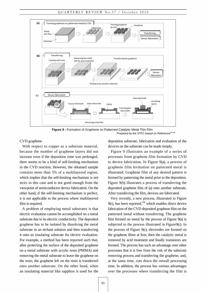
CVD graphene. With respect to copper as a substrate material, because the number of graphene layers did not increase even if the deposition time was prolonged, there seems to be a kind of self-limiting mechanism in the CVD reaction. However, the obtained sample contains more than 5% of a multilayered region, which implies that the self-limiting mechanism is not strict in this case and is not good enough from the viewpoint of semiconductor device fabrication. On the other hand, if the self-limiting mechanism is perfect, it is not applicable to the process where multilayered fi lm is required. A problem of employing metal substrates is that electric evaluation cannot be accomplished on a metal substrate due to its electric conductivity. The deposited graphene has to be isolated by dissolving the metal substrate in an etchant solution and then transferring it onto an insulating substrate for electric evaluation. For example, a method has been reported such that, after protecting the surface of the deposited graphene on a metal substrate with acrylic resin (PMMA) and removing the metal substrate to leave the graphene on the resin, the graphene left on the resin is transferred onto another substrate. On the other hand, when an insulating material like sapphire is used for the
deposition substrate, fabrication and evaluation of the devices on the substrate can be made simply. Figure 9 illustrates an example of a series of processes from graphene film formation by CVD to device fabrication. In Figure 9(a), a process of graphene film formation on patterned metal is illustrated. Graphene film of any desired pattern is formed by patterning the metal prior to the deposition. Figure 9(b) illustrates a process of transferring the deposited graphene fi lm of (a) onto another substrate. After transferring the fi lm, devices are fabricated. Very recently, a new process, illustrated in Figure 9(c), has been reported,[18] which enables direct device fabrication of the CVD deposited graphene fi lm on the patterned metal without transferring. The graphene fi lm formed on metal by the process of Figure 9(a) is subjected to the process illustrated in Figure9(c). In the process of Figure 9(c), electrodes are formed on the graphene fi lms at fi rst, then the catalytic metal is removed by acid treatment and fi nally transistors are formed. The process has such an advantage over other processes that it is free from the risk of the substrate removing process and transferring the graphene, and, at the same time, cuts down the overall processing time. In addition, the process has various advantages over the processes where transferring the film is
Figure 9 : Formation of Graphene on Patterned Catalytic Metal Thin FilmPrepared by the STFC based on Reference[16,18]
��������
����
� �������
���������
������������ ���
������
��������� ������
��������������������
������������� ����� �
��� �
��������!�� �����
���
���
����������� � ����� �� �� �������
����� �����
����� �����
� ��� ���������
� ���
��������
����
� �������
���������
������������ ���
������
��������� ������
��������������������
������������� ����� �
����"������������� ����������
��� �
�����������������
������������������
������������
�������
#����������
�����
���������
������������
��������!�� �����
���
���
���
����������� � ����� �� �� �������
����� �����
� ��� ���������
����� �����
� ��� ���������
� ���
���������
86
S C I E N C E & T E C H N O L O G Y T R E N D S
necessary, because it enables performing a series of processes continuously on a desired substrate. It is probable that this new process would be standard for the fabrication of transistors.
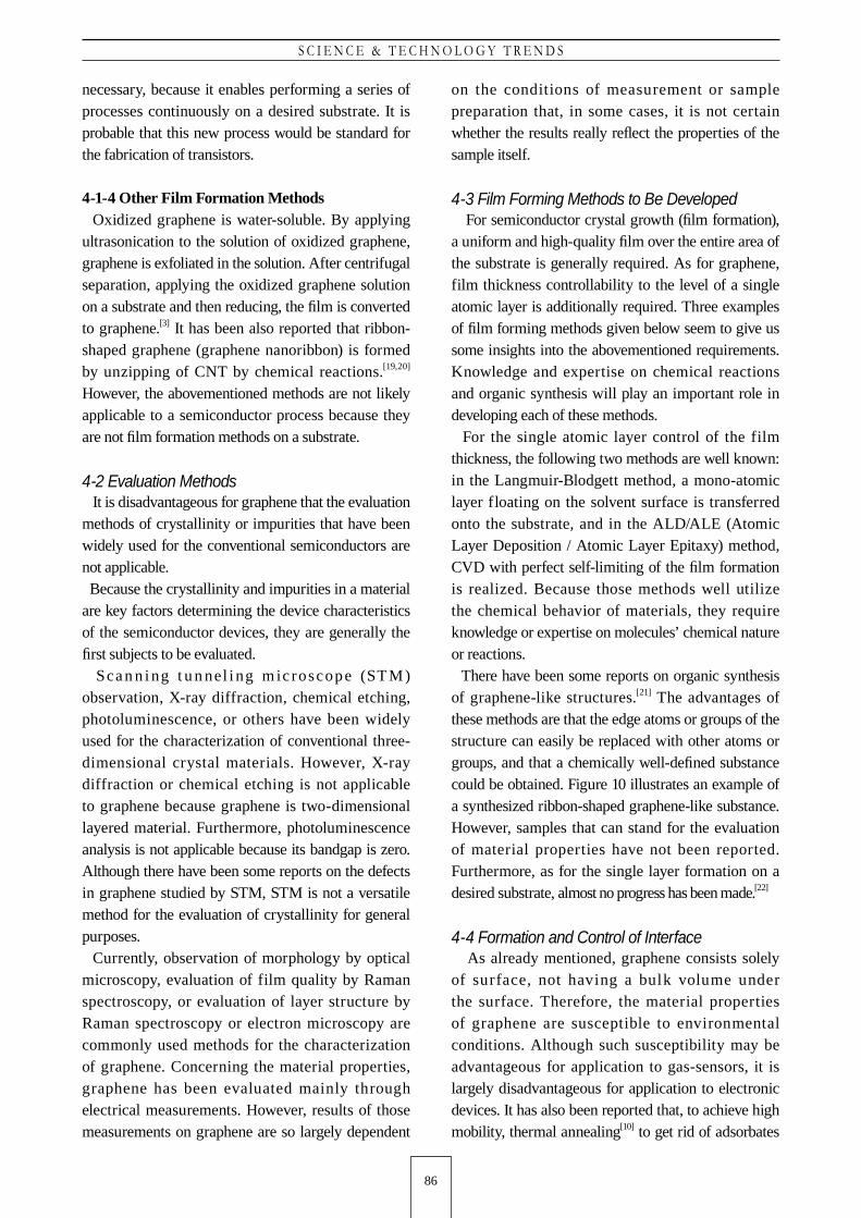
4-1-4 Other Film Formation Methods Oxidized graphene is water-soluble. By applying ultrasonication to the solution of oxidized graphene, graphene is exfoliated in the solution. After centrifugal separation, applying the oxidized graphene solution on a substrate and then reducing, the fi lm is converted to graphene.[3] It has been also reported that ribbon-shaped graphene (graphene nanoribbon) is formed by unzipping of CNT by chemical reactions.[19,20]
However, the abovementioned methods are not likely applicable to a semiconductor process because they are not fi lm formation methods on a substrate.
4-2 Evaluation Methods It is disadvantageous for graphene that the evaluation methods of crystallinity or impurities that have been widely used for the conventional semiconductors are not applicable. Because the crystallinity and impurities in a material are key factors determining the device characteristics of the semiconductor devices, they are generally the fi rst subjects to be evaluated. Sca n n i ng t u n nel i ng m ic roscope (ST M ) observation, X-ray diffraction, chemical etching, photoluminescence, or others have been widely used for the characterization of conventional three-dimensional crystal materials. However, X-ray diffraction or chemical etching is not applicable to graphene because graphene is two-dimensional layered material. Furthermore, photoluminescence analysis is not applicable because its bandgap is zero. Although there have been some reports on the defects in graphene studied by STM, STM is not a versatile method for the evaluation of crystallinity for general purposes. Currently, observation of morphology by optical microscopy, evaluation of film quality by Raman spectroscopy, or evaluation of layer structure by Raman spectroscopy or electron microscopy are commonly used methods for the characterization of graphene. Concerning the material properties, graphene has been evaluated mainly through electrical measurements. However, results of those measurements on graphene are so largely dependent
on the conditions of measurement or sample preparation that, in some cases, it is not certain whether the results really refl ect the properties of the sample itself.
4-3 Film Forming Methods to Be Developed For semiconductor crystal growth (fi lm formation), a uniform and high-quality fi lm over the entire area of the substrate is generally required. As for graphene, film thickness controllability to the level of a single atomic layer is additionally required. Three examples of fi lm forming methods given below seem to give us some insights into the abovementioned requirements. Knowledge and expertise on chemical reactions and organic synthesis will play an important role in developing each of these methods. For the single atomic layer control of the film thickness, the following two methods are well known: in the Langmuir-Blodgett method, a mono-atomic layer floating on the solvent surface is transferred onto the substrate, and in the ALD/ALE (Atomic Layer Deposition / Atomic Layer Epitaxy) method, CVD with perfect self-limiting of the fi lm formation is realized. Because those methods well utilize the chemical behavior of materials, they require knowledge or expertise on molecules’ chemical nature or reactions. There have been some reports on organic synthesis of graphene-like structures.[21] The advantages of these methods are that the edge atoms or groups of the structure can easily be replaced with other atoms or groups, and that a chemically well-defi ned substance could be obtained. Figure 10 illustrates an example of a synthesized ribbon-shaped graphene-like substance. However, samples that can stand for the evaluation of material properties have not been reported. Furthermore, as for the single layer formation on a desired substrate, almost no progress has been made.[22]
4-4 Formation and Control of Interface As already mentioned, graphene consists solely of surface, not having a bulk volume under the surface. Therefore, the material properties of graphene are susceptible to environmental conditions. Although such susceptibility may be advantageous for application to gas-sensors, it is largely disadvantageous for application to electronic devices. It has also been reported that, to achieve high mobility, thermal annealing[10] to get rid of adsorbates
Q U A R T E R L Y R E V I E W N o . 3 7 / O c t o b e r 2 0 1 0
87
is important. Therefore, practical devices would not be available without preparing countermeasures against environmental disturbance. Concerning influence from the environment, the properties of graphene are also influenced by the substrate as well as by the adsorbates. For example, it has been reported that one order of magnitude higher mobility was obtained[10] by suspending the graphene sample off of the substrate like a bridge, compared to the case where graphene directly contacts the substrate. It is considered that the impurities in the substrate cause decrease in mobility when the graphene has direct contact with the substrate. From a practical point of view, development of protecting films against atmospheric interference which do not affect the material properties is crucial.
Research and Engineering on Graphene-based Electronic Devices: Current Status and Trends
In this chapter, control methods of bandgap of graphene will be described fi rst, and then an overview on graphene-based electronic devices of which application has been studied will be given. The electronic devices are a fi eld effect transistor utilizing high mobility of graphene, a single-electron transistor utilizing switching capability by loss or gain of single electron, and a spin-transport device which transports an electron’s spin-state.
5-1 Opening and Tuning of Bandgap As mentioned in 2-1, the zero bandgap of graphene makes it hard to be applied to digital devices which require a high switching on/off ratio. Two techniques
listed below are mainly studied for opening the bandgap.
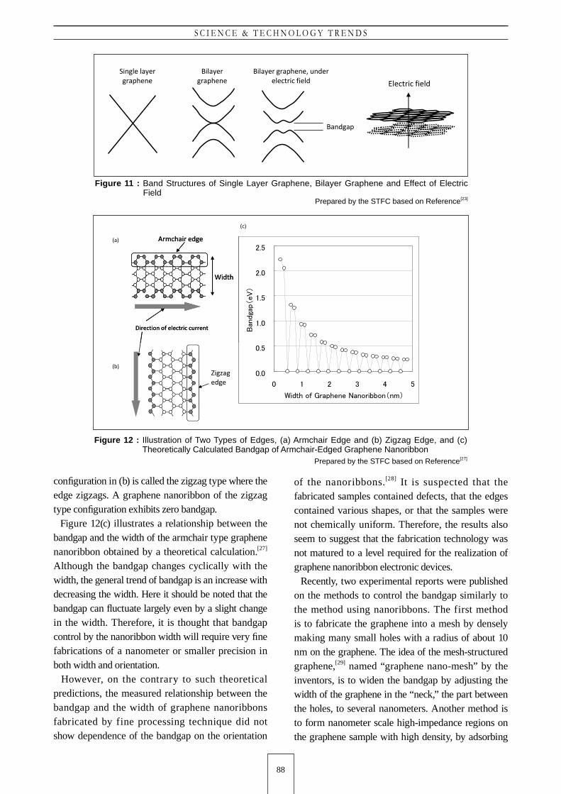
5-1-1 Bilayer Graphene Bilayer graphene is a lamination of two layers of graphene. Although the bandgap of bilayer graphene is still zero, it can be opened by applying an external electric fi eld across the bilayer graphene (Figure 11). Adsorption of atoms such as potassium on the bilayer graphene is also effective for opening the bandgap similarly. Usually a band gap is a material parameter which is determined uniquely to each material as shown in Figure 7(c). In this respect, the method where an electric fi eld is applied to bilayer graphene is not only advantageous but also of great interest in that the bandgap is tunable by the applied fi eld strength. It has been reported that the bandgap was tuned up to about 0.3 eV.[23] According to another report,[24] widening of the bandgap has also been confirmed by measuring electric properties of the transistors fabricated by using bilayer graphene. It is known that the electron mobility in bilayer graphene is lower than that of single layer graphene. A computer simulation,[25] however, reported that transistors based on such bilayer graphene would perform high speed operation as fast as HEMT (High Electron Mobility Transistor) made of InP which is a compound semiconductor known for its high electron mobility.
5-1-2 Graphene Nanoribbon Another technique for opening the bandgap of graphene is to decrease the width of a graphene sheet. Graphene is called a graphene nanoribbon when the width of the graphene is several times the unit cell of graphene. Theoretical calculations[26] on the band structure of graphene nanoribbons have shown that graphene nanoribbons exhibit metallic properties or semiconductor properties, i.e. the bandgap is larger than 0, depending on the orientation of the ribbon. Two confi gurations of graphene nanoribbon structure are illustrated in Figure 12 (a) and (b) focusing on the edges of graphene nanoribbons. The configuration illustrated in (a) is called the armchair type where the edge has a cyclic structure of four carbon atoms, i.e. two couples of carbon atoms. A graphene nanoribbon of the armchair type conf iguration exhibits semiconductor properties. On the other hand, the
Figure 10 : Molecular Structure of Ribbon-Shaped Graphene-Like Substance Obtained by Organic Synthesis
Prepared by the STFC based on Reference[21]
5
n=6 12n
88
S C I E N C E & T E C H N O L O G Y T R E N D S
confi guration in (b) is called the zigzag type where the edge zigzags. A graphene nanoribbon of the zigzag type confi guration exhibits zero bandgap. Figure 12(c) illustrates a relationship between the bandgap and the width of the armchair type graphene nanoribbon obtained by a theoretical calculation.[27] Although the bandgap changes cyclically with the width, the general trend of bandgap is an increase with decreasing the width. Here it should be noted that the bandgap can fl uctuate largely even by a slight change in the width. Therefore, it is thought that bandgap control by the nanoribbon width will require very fi ne fabrications of a nanometer or smaller precision in both width and orientation. However, on the contrary to such theoretical predictions, the measured relationship between the bandgap and the width of graphene nanoribbons fabricated by fine processing technique did not show dependence of the bandgap on the orientation
of the nanoribbons.[28] It is suspected that the fabricated samples contained defects, that the edges contained various shapes, or that the samples were not chemically uniform. Therefore, the results also seem to suggest that the fabrication technology was not matured to a level required for the realization of graphene nanoribbon electronic devices. Recently, two experimental reports were published on the methods to control the bandgap similarly to the method using nanoribbons. The first method is to fabricate the graphene into a mesh by densely making many small holes with a radius of about 10 nm on the graphene. The idea of the mesh-structured graphene,[29] named “graphene nano-mesh” by the inventors, is to widen the bandgap by adjusting the width of the graphene in the “neck,” the part between the holes, to several nanometers. Another method is to form nanometer scale high-impedance regions on the graphene sample with high density, by adsorbing
Bandgap
Electric field
Single layer graphene
Bilayer graphene
Bilayer graphene, under electric field
Figure 11 : Band Structures of Single Layer Graphene, Bilayer Graphene and Effect of Electric Field
Prepared by the STFC based on Reference[23]
Figure 12 : Illustration of Two Types of Edges, (a) Armchair Edge and (b) Zigzag Edge, and (c) Theoretically Calculated Bandgap of Armchair-Edged Graphene Nanoribbon
Prepared by the STFC based on Reference[27]
���
��� ����������
����
������������������� ����
���
���
���
������������
���
���
���
������������
���
����������
������
��
����
������������������� ����
���
���
���
���
���
���
� � � � � �
�� �������� �����������������
���������
���
���
���
���
���
���
� � � � � �
�� �������� �����������������
���������
Q U A R T E R L Y R E V I E W N o . 3 7 / O c t o b e r 2 0 1 0
89
hydrogen atoms locally on the surface of the graphene sample.[30] Unlike the nanoribbon method, neither of the two methods requires narrowing the width of the original graphene sheet. Therefore, the graphene made by those methods can endure high electric current, and the handling of these substances is easier than nanoribbons. According to these advantages over nanoribbons, attention will be paid to their development.
5-2 Field Effect Transistor The field effect transistor (FET) is a key element of LSI, where the current flowing through a thin channel layer is controlled by gate electrodes. FET can be operated faster with a channel layer of a higher electron mobility material, which is the very point of the application of graphene to FET. There are some reports on the characteristics of FET using graphene as a channel layer material. For the fabrication of graphene-based FET, graphene exfoliated from HOPG is often used. On the other hand, a recent report on 100 gigahertz operation[4] of a FET based on graphene by heat-treatment of SiC, has been a major topic. The operation speed is already more than twice higher than that of silicon-based FET which uses silicon as the channel layer with the same gate length. It strongly indicates the high potentiality of graphene application to FET. In addition, the mobility of graphene used in these reports is not so high compared with that expected of typical graphene samples. In another report,[31] it was mentioned that the mobility was lowered to a great extent after processing for FET fabrication. It suggests that, establishing a process that can preserve the high mobility that graphene originally possesses, and improvement of the FET structure matched to the properties of graphene, will make graphene-based FET terahertz operation possible, which has not been realized by FETs based on other materials.
5-3 Single-Electron Transistor Electronic states of metals or semiconductors sized some nanometers three-dimensionally can be changed drastically by injecting only a single electron into it. Such a very small structure is called a quantum dot. The electronic states of a quantum dot can be controlled also by controlling the electric potential of the quantum dot. The single electron transistor (SET) is based on the idea of controlling the number
of electrons in a quantum dot by its electric potential. The energy consumption of SET is thought to be very small, because the unit of information is a single electron. Therefore, SET is expected to be a transistor which will be used widely in the future, and many research efforts have been put into it.
There are some reports on application of graphene to SET, and switching at room temperature has been reported.[6] Graphene has a potential advantage that quantum dots can be easily formed just by cutting out small regions by etching, because graphene originally has only a single atomic layer thickness. However, controllable fabrication with a precision of several nanometers still remains as a challenge. For example, the switching performance at room temperature is not well reproducible yet due to the lack of precise fabrication technology.
5-4 Spin Transport Device In the spin transport device, information is carried as a form of fl ow of electron-spin polarity. It has been thought that such a device has various advantages over the conventional devices using electric current, and several materials have been research targets. Graphene has been expected to be applied to the spin transport device, for the reason that the spin polarity of an electron in graphene is less perturbed by nuclei because graphene contains only carbon atoms, one of the light elements. A report[5] has already experimentally shown that spin injection into graphene is attainable. Furthermore, it has been observed that the electrons diffuse in graphene keeping the spin polarity. It is certain that graphene is considered to be one of the promising candidate materials for the spin transport device.
Conclusions
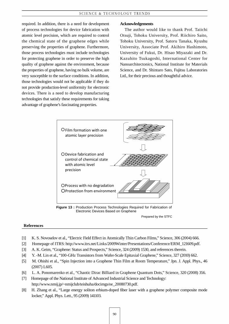
In recent years, graphene has attracted attention as a promising material for advanced electronic devices including high speed transistors which play a central role in LSI technology, and the number of articles on graphene has been increasing rapidly. However, in reality, the technologies of fabrication or processing are far from the level expected for the actual production of devices for practical use. As for such fabrication technologies, film forming process technologies with one-atom thickness precision are
6
90
S C I E N C E & T E C H N O L O G Y T R E N D S
required. In addition, there is a need for development of process technologies for device fabrication with atomic level precision, which are required to control the chemical state of the graphene edges while preserving the properties of graphene. Furthermore, those process technologies must include technologies for protecting graphene in order to preserve the high quality of graphene against the environment, because the properties of graphene, having no bulk volume, are very susceptible to the surface conditions. In addition, those technologies would not be applicable if they do not provide production-level uniformity for electronic devices. There is a need to develop manufacturing technologies that satisfy these requirements for taking advantage of graphene’s fascinating properties.
Acknowledgements The author would like to thank Prof. Taiichi Otsuji, Tohoku University, Prof. Riichiro Saito, Tohoku University, Prof. Satoru Tanaka, Kyushu University, Associate Prof. Akihiro Hashimoto, University of Fukui, Dr. Hisao Miyazaki and Dr. Kazuhito Tsukagoshi, International Center for Nanoarchitectonics, National Institute for Materials Science, and Dr. Shintaro Sato, Fujitsu Laboratories Ltd., for their precious and thoughtful advice.
Device fabrication and control of chemical state with atomic level precision
Process with no degradationProtection from environment
Film formation with one atomic layer precision
Figure 13 : Production Process Technologies Required for Fabrication of Electronic Devices Based on Graphene
Prepared by the STFC
[1] K. S. Novoselov et al., “Electric Field Effect in Atomically Thin Carbon Films,” Science, 306 (2004) 666.[2] Homepage of ITRS: http://www.itrs.net/Links/2009Winter/Presentations/Conference/ERM_121609.pdf.[3] A. K. Geim, “Graphene: Status and Prospects,” Science, 324 (2009) 1530, and references therein.[4] Y. -M. Lin et al., “100-GHz Transistors from Wafer-Scale Epitaxial Graphene,” Science, 327 (2010) 662.[5] M. Ohishi et al., “Spin Injection into a Graphene Thin Film at Room Temperature,” Jpn. J. Appl. Phys., 46
(2007) L605.[6] L. A. Ponomarenko et al., “Chaotic Dirac Billiard in Graphene Quantum Dots,” Science, 320 (2008) 356.[7] Homepage of the National Institute of Advanced Industrial Science and Technology:
http://www.nmij.jp/~nmijclub/teishuha/docimgs/oe_20080730.pdf.[8] H. Zhang et al., “Large energy soliton erbium-doped fi ber laser with a graphene polymer composite mode
locker,” Appl. Phys. Lett., 95 (2009) 141103.
References
Q U A R T E R L Y R E V I E W N o . 3 7 / O c t o b e r 2 0 1 0
91
[9] “Group III-V Compound Semiconductors” I-1, Advanced Electronics Series, authored and edited by Isamu Akasaki, Baifukan, 2002 (Japanese), Refer to chapter 13 for GaN and chapter 7 for others.
[10] M. Orlita et al., “Approaching the Dirac Point in High-Mobility Multilayer Epitaxial Graphene,” Phys. Rev. Lett., 101 (2008) 267601.
[11] K. I. Bolotin et al., “Ultrahigh electron mobility in suspended graphene,” Solid State Commun., 146 (2008) 351.
[12] A. K. Geim et al., “Carbon Wonderland,” Scientifi c American, 298 (2008) 90.[13] K. V. Emtsev et al., “Toward wafer-size graphene layers by atmospheric pressure graphitization of silicon
carbide,” Nature Mater., 8 (2009) 203.[14] Y. Miyamoto et al., “Raman-Scattering Spectroscopy of Epitaxial Graphene Formed on SiC Film on Si
Substrate,” e-Journal of Surface Science and Nanotechnology, 7 (2009) 107.[15] X. Li et al., “Large-Area Synthesis of High-Quality and Uniform Graphene Films on Copper Foils,” Science,
324 (2009) 1312.[16] K. S. Kim et al., “Large-scale pattern growth of graphene fi lms for stretchable transparent electrodes,” Nature,
457 (2009) 706.[17] Makoto Okai et al., “Growth of Graphene on Sapphire Substrate by Thermal CVD,” the 70th Fall Meeting,
2009 11p-ZR-3, Japan Society of Applied Physics (Japanese).[18] D. Kondo et al., “Low-Temperature Synthesis of Graphene and Fabrication of Top-Gated Field Effect
Transistors without Using Transfer Processes,” Appl. Phys. Exp., 3 (2010) 025102.[19] D. V. Kosynkin et al., “Longitudinal unzipping of carbon nanotubes to form graphene nanoribbons,” Nature,
458 (2009) 872.[20] L. Jiao et al., “Narrow graphene nanoribbons from carbon nanotubes,” Nature, 458 (2009) 877.[21] Kentaro Satoh, “Chemical Synthesis Challenges New Carbon Materials from Graphene to Nanotubes,” Gendai
Kagaku (Modern Chemistry), August 2009, pp.16-20, and references therein (Japanese). See also, X. Yang et al., “Two-Dimensional Graphene Nanoribbons,” J. Am. Chem. Soc., 130 (4216) 2008.
[22] Shortly after the publication of the original Japanese version of the present article, a report on the synthesis of graphene nanoribbons from monomers on a metal surface, was published; J. Cai et al., “Atomically precise bottom-up fabrication of graphene nanoribbons,” Nature 466 (2010) 470.
[23] Y. Zhang et al., “Direct observation of a widely tunable bandgap in Bilayer graphene,” Nature, 459 (2009) 820.[24] Hisao Miyazaki et al., “Bandgap Engineering of Bilayer Graphene Induced by Electric Field,” the 56th Spring
Meeting, 2009, 1a-ZA-3, Japan Society of Applied Physics (Japanese).[25] N. Harada et al., “Performance Estimation of Graphene Field-Effect Transistors Using Semiclassical Monte
Carlo Simulation,” Appl. Phys. Exp., 1 (2008) 024002.[26] K. Nakada et al., “Edge state in graphene ribbons: Nanometer size effect and edge shape dependence,” Phys.
Rev. B., 54 (1996) 17954.[27] Y. -W. Son et al., “Energy Gaps in Graphene Nanoribbons,” Phys. Rev. Lett., 97 (2006) 216803.[28] M. Y. Han et al., “ Energy Band-Gap Engineering of Graphene Nanoribbons,” Phys. Rev. Lett., 98 (2007)
206805.[29] J. Bai et al., “Graphene nanomesh,” Nature Nanotech., 5 (2010) 190.[30] R. Balog et al., “Bandgap opening in graphene induced by patterned hydrogen adsorption,” Nature Mater., 9
(2010) 315.[31] Y. Lin et al., “Operation of Graphene Transistors at Gigahertz Frequencies,” Nano Lett., 9 (2009) 422.

92
S C I E N C E & T E C H N O L O G Y T R E N D S
(Original Japanese version: published in May 2010)
Profi le
Yasushi IYECHIKASpecial Researcher, Nanotechnology and Materials Research Unit, STFChttp://www.nistep.go.jp/index-j.html
He was engaged in technological development of the blue LED and its patent applications at a chemical company, and the development of a production-scale MOCVD system at a venture company. At present, he is with an analytical instrument manufacturer. He is interested in nanotechnology and materials because it is a basic technological fi eld and is applied to various fi elds.