poly-4-vinylphenol and poly(melamine-co-formaldehyde)-based graphene passivation method for...
TRANSCRIPT
Nanoscale
PAPER
Publ
ishe
d on
08
Janu
ary
2014
. Dow
nloa
ded
by S
ungk
yunk
wan
Uni
vers
ity o
n 16
/06/
2014
05:
20:3
4.
View Article OnlineView Journal | View Issue
aSamsung-SKKU Graphene Center, Su
Nanotechnology (SAINT) and School of
Sungkyunkwan University, Suwon 440-7
[email protected]; Tel: +82-31-290-7970bDepartment of Electrical Engineering, StanfcIBM Thomas J. Watson Research Center, YodSchool of Advanced Materials Science and
Nanotechnology (SAINT), Center for Hum
SKKU-Samsung Graphene Center, Sungkyun
† Equally contributed as the rst author.
Cite this: Nanoscale, 2014, 6, 3830
Received 9th December 2013Accepted 30th December 2013
DOI: 10.1039/c3nr06517k
www.rsc.org/nanoscale
3830 | Nanoscale, 2014, 6, 3830–3836
Poly-4-vinylphenol and poly(melamine-co-formaldehyde)-based graphene passivationmethod for flexible, wearable and transparentelectronics
In-yeal Lee,†a Hyung-Youl Park,†a Jin-hyung Park,a Gwangwe Yoo,a
Myung-Hoon Lim,a Junsung Park,a Servin Rathi,a Woo-Shik Jung,b Jeehwan Kim,c
Sang-Woo Kim,d Yonghan Roh,a Gil-Ho Kim*a and Jin-Hong Park*a
Next generation graphene-based electronics essentially need a dielectric layer with several requirements
such as high flexibility, high transparency, and low process temperature. Here, we propose and
investigate a flexible and transparent poly-4-vinylphenol and poly(melamine-co-formaldehyde) (PVP/
PMF) insulating layer to achieve intrinsic graphene and an excellent gate dielectric layer at sub 200 �C.Chemical and electrical effects of PVP/PMF layer on graphene as well as its dielectric property are
systematically investigated through various measurements by adjusting the ratio of PVP to PMF and
annealing temperature. The optimized PVP/PMF insulating layer not only removes the native –OH
functional groups which work as electron-withdrawing agents on graphene (Dirac point close to zero)
but also shows an excellent dielectric property (low hysteresis voltage). Finally, a flexible, wearable, and
transparent (95.8%) graphene transistor with Dirac point close to zero is demonstrated on polyethylene
terephthalate (PET) substrate by exploiting PVP/PMF layer which can be scaled down to 20 nm.
1. Introduction
Next generation exible, wearable, and transparent electronics(FWTEs) such as electronic-paper, wearable display, exibletouch screen, and transparent wall, are expected to bemechanically exible, optically transparent, and light inweight.1–4 For the transistors that these devices are fundamen-tally composed of, novel materials such as indium tin oxide(ITO), zinc tin oxide (ZTO), carbon nano tube (CNT), and poly-imide have been previously proposed as electrode, activechannel, and dielectric layers.5–10 Although zero band gap gra-phene is limited in the present situation for complementarymetal–oxide–semiconductor (CMOS) applications due to its lowon/off-current ratio and high power consumption, it is still apromising candidate for FWTEs because of its high mobility(�200 000 cm2 V s�1), exibility (fracture strain of 30%), and
ngkyunkwan Advanced Institute of
Electronics and Electrical Engineering,
46, Korea. E-mail: [email protected];
ord University, Stanford, CA 94305, USA
rktown Heights, New York 10598, USA
Engineering, SKKU Advanced Institute of
an Interface Nanotechnology (HINT),
kwan University, Suwon 440-746, Korea
transparency (97.5% for monolayer).11–14 However, two criticalissues need to be resolved before utilizing graphene as a FWTEsmaterial; nding a exible and transparent insulator for gatedielectric and maintaining its intrinsic electrical property.
Recently, 2D dielectrics such as boron nitride (BN) and micahave been applied for graphene-based devices because of lowroughness, reduction of interfacial carrier scattering, and betterscale-down potential for future devices.15 However, it is still achallenge to achieve large area BN and mica-based devices areincompatible with exible electronics. Another insulatingmaterials such as ion gel, high-k dielectric, and graphite oxide(GO) have been also studied for the graphene-based FWTEs.16–19
Even though these insulators show good electrical combinationwith graphene, high cost of raw materials for ion gel, non-uniformity of the GO layer, and high thermal processing ofhigh-k dielectric layer are hindering the successful integrationof graphene-based FWTEs. In addition, it is a challenging taskto achieve graphene layers with intrinsic property where theconcentration of holes and electrons are symmetric. The root ofthese issues lies in the unexpected doping problem on graphenesurface caused by native hydroxyl (–OH) functional groupsunder atmospheric ambient and polymer-residues depositedduring the fabrication process.20–26 Because the p-type dopingproblem degrades the performance of graphene-based devices,several methods such as encapsulation by BN, vacuum anneal,and chemical cleaning process, have been proposed to remove
This journal is © The Royal Society of Chemistry 2014
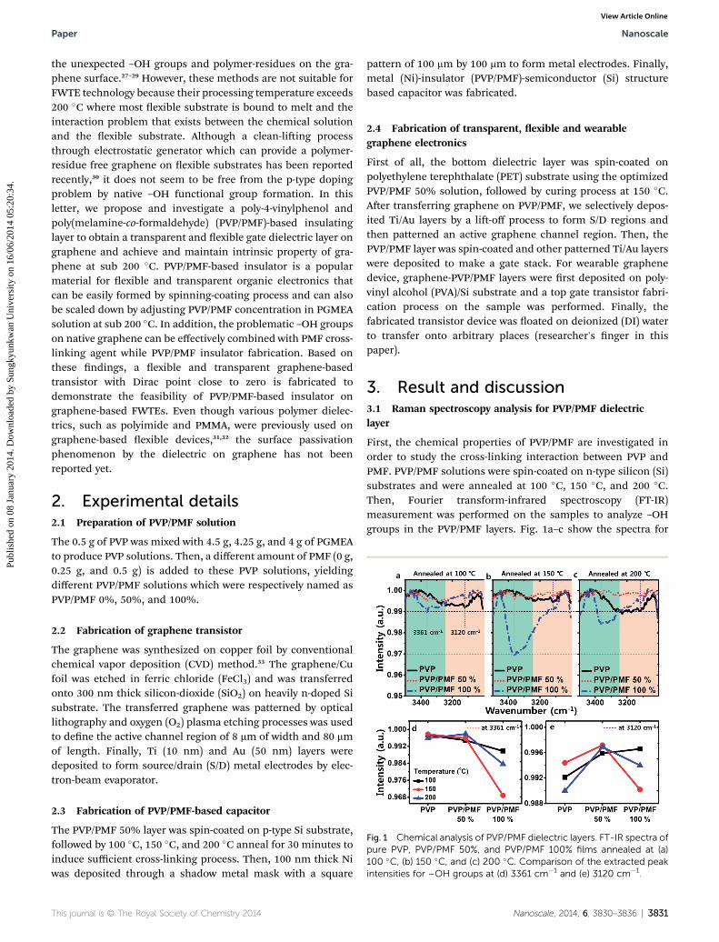
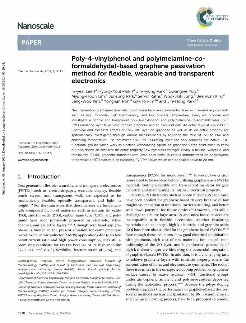
Fig. 1 Chemical analysis of PVP/PMF dielectric layers. FT-IR spectra ofpure PVP, PVP/PMF 50%, and PVP/PMF 100% films annealed at (a)100 �C, (b) 150 �C, and (c) 200 �C. Comparison of the extracted peakintensities for –OH groups at (d) 3361 cm�1 and (e) 3120 cm�1.
Paper Nanoscale
Publ
ishe
d on
08
Janu
ary
2014
. Dow
nloa
ded
by S
ungk
yunk
wan
Uni
vers
ity o
n 16
/06/
2014
05:
20:3
4.
View Article Online
the unexpected –OH groups and polymer-residues on the gra-phene surface.27–29 However, these methods are not suitable forFWTE technology because their processing temperature exceeds200 �C where most exible substrate is bound to melt and theinteraction problem that exists between the chemical solutionand the exible substrate. Although a clean-liing processthrough electrostatic generator which can provide a polymer-residue free graphene on exible substrates has been reportedrecently,30 it does not seem to be free from the p-type dopingproblem by native –OH functional group formation. In thisletter, we propose and investigate a poly-4-vinylphenol andpoly(melamine-co-formaldehyde) (PVP/PMF)-based insulatinglayer to obtain a transparent and exible gate dielectric layer ongraphene and achieve and maintain intrinsic property of gra-phene at sub 200 �C. PVP/PMF-based insulator is a popularmaterial for exible and transparent organic electronics thatcan be easily formed by spinning-coating process and can alsobe scaled down by adjusting PVP/PMF concentration in PGMEAsolution at sub 200 �C. In addition, the problematic –OH groupson native graphene can be effectively combined with PMF cross-linking agent while PVP/PMF insulator fabrication. Based onthese ndings, a exible and transparent graphene-basedtransistor with Dirac point close to zero is fabricated todemonstrate the feasibility of PVP/PMF-based insulator ongraphene-based FWTEs. Even though various polymer dielec-trics, such as polyimide and PMMA, were previously used ongraphene-based exible devices,31,32 the surface passivationphenomenon by the dielectric on graphene has not beenreported yet.
2. Experimental details2.1 Preparation of PVP/PMF solution
The 0.5 g of PVP was mixed with 4.5 g, 4.25 g, and 4 g of PGMEAto produce PVP solutions. Then, a different amount of PMF (0 g,0.25 g, and 0.5 g) is added to these PVP solutions, yieldingdifferent PVP/PMF solutions which were respectively named asPVP/PMF 0%, 50%, and 100%.
2.2 Fabrication of graphene transistor
The graphene was synthesized on copper foil by conventionalchemical vapor deposition (CVD) method.33 The graphene/Cufoil was etched in ferric chloride (FeCl3) and was transferredonto 300 nm thick silicon-dioxide (SiO2) on heavily n-doped Sisubstrate. The transferred graphene was patterned by opticallithography and oxygen (O2) plasma etching processes was usedto dene the active channel region of 8 mm of width and 80 mmof length. Finally, Ti (10 nm) and Au (50 nm) layers weredeposited to form source/drain (S/D) metal electrodes by elec-tron-beam evaporator.
2.3 Fabrication of PVP/PMF-based capacitor
The PVP/PMF 50% layer was spin-coated on p-type Si substrate,followed by 100 �C, 150 �C, and 200 �C anneal for 30 minutes toinduce sufficient cross-linking process. Then, 100 nm thick Niwas deposited through a shadow metal mask with a square
This journal is © The Royal Society of Chemistry 2014
pattern of 100 mm by 100 mm to form metal electrodes. Finally,metal (Ni)-insulator (PVP/PMF)-semiconductor (Si) structurebased capacitor was fabricated.
2.4 Fabrication of transparent, exible and wearablegraphene electronics
First of all, the bottom dielectric layer was spin-coated onpolyethylene terephthalate (PET) substrate using the optimizedPVP/PMF 50% solution, followed by curing process at 150 �C.Aer transferring graphene on PVP/PMF, we selectively depos-ited Ti/Au layers by a li-off process to form S/D regions andthen patterned an active graphene channel region. Then, thePVP/PMF layer was spin-coated and other patterned Ti/Au layerswere deposited to make a gate stack. For wearable graphenedevice, graphene-PVP/PMF layers were rst deposited on poly-vinyl alcohol (PVA)/Si substrate and a top gate transistor fabri-cation process on the sample was performed. Finally, thefabricated transistor device was oated on deionized (DI) waterto transfer onto arbitrary places (researcher's nger in thispaper).
3. Result and discussion3.1 Raman spectroscopy analysis for PVP/PMF dielectriclayer
First, the chemical properties of PVP/PMF are investigated inorder to study the cross-linking interaction between PVP andPMF. PVP/PMF solutions were spin-coated on n-type silicon (Si)substrates and were annealed at 100 �C, 150 �C, and 200 �C.Then, Fourier transform-infrared spectroscopy (FT-IR)measurement was performed on the samples to analyze –OHgroups in the PVP/PMF layers. Fig. 1a–c show the spectra for
Nanoscale, 2014, 6, 3830–3836 | 3831
Nanoscale Paper
Publ
ishe
d on
08
Janu
ary
2014
. Dow
nloa
ded
by S
ungk
yunk
wan
Uni
vers
ity o
n 16
/06/
2014
05:
20:3
4.
View Article Online
–OH groups in PVP/PMF layers, which are typically locatedbetween 3000 cm�1 and 3400 cm�1. In the pure PVP samplewithout PMF, we found that the peak for –OH groups wasaround 3000 cm�1 to 3250 cm�1. However, other peaks relatingto –OH groups in PVP/PMF 50% and PVP/PMF 100% sampleswere observed at 3250 cm�1 to 3450 cm�1. The reason for thedifferent peak positions is related to the cross-linking mecha-nism between PVP and PMF, which makes PVP molecules tobond with PMF through –OH and –OH bonding during theannealing process, thereby reducing the number of –OH groupsin PVP. As a result, –OH groups in the pure PVP and PVP/PMFlms are respectively in non-hydrogen and hydrogen bondingstates.29 The difference of bonding states makes the peaks to belocated at the slightly different positions. In the case of PVP/PMF 50%, as shown in Fig. 1d and e, very low and stable peakintensities were observed at all annealing temperaturescompared to the PVP/PMF 100% sample, indicating that aproper concentration of PMF was mixed to cross-link with the–OH groups in PVP. It is predicted that high and unstableintensities of PVP/PMF 100% sample is attributed to theremaining –OH groups of PMF remaining aer the cross-linkingprocess.
3.2 Electrical analysis for PVP/PMF dielectric depositedgraphene transistor with different PMF concentration
The PVP/PMF cross-linking process was then applied on thegraphene surface by depositing and annealing PVP/PMF layers.Fig 2a shows the schematic diagram of the fabricated graphenetransistor and possible chemical reactions among –OH groupsin graphene, PVP, and PMF. As widely known, native –OHgroups are easily formed on graphene surface under
Fig. 2 Schematic diagram for possible chemical interactions andcarrier transporting properties of graphene devices passivated by PVP/PMF with different PMF concentrations. (a) Schematic diagrams offabricated graphene transistor, indicating chemical reactions by PVPand PMF on graphene. (b) ID–VG characteristics of graphene transistorsexposed to air and encapsulated by pure PVP, PVP/PMF 50%, and PVP/PMF 100% films (all of the samples were annealed at 200 �C). (c)Distribution of Dirac points extracted from the ID–VG characteristics of10 transistor samples for each annealing temperature.
3832 | Nanoscale, 2014, 6, 3830–3836
atmospheric condition, making the graphene layer to work as p-type materials.23 Although there was an experimental report thatthe type of graphene converts to intrinsic through vacuumannealing process at 200 �C, very high positive Dirac point value(�50 V) was still obtained in the graphene sample annealed at200 �C meaning that the graphene is still strong p-type.28
However, in the graphene transistors with PVP, PVP/PMF 50%,and PVP/PMF 100% layers, Dirac points were respectively shif-ted to 27 V, 6 V, and �2 V aer the 200 �C anneal. It is thoughtthat –OH groups in PVP and PVP/PMF are bonded with those ongraphene surface during the annealing process, thus reducingthe number of –OH groups on graphene. It seems that this effectis stronger as the PMF concentration increases in PVP solution.This observation suggests that the cross-linking process with–OH groups on graphene by PMF is expected to be morefavorable than that by PVP at 200 �C. In order to re-verify theshiing of Dirac point according to different concentration ofPMF, drain current–gate voltage (ID–VG) measurement andDirac point extraction were performed on ten different gra-phene transistor devices, as shown in Fig. 2b and c. Here, it isconrmed that PVP/PMF layer can effectively reduce thenumber of –OH groups on graphene surface through theannealing process and PVP/PMF 50% is optimal in obtainingthe intrinsic property of graphene with Dirac point at �0 V andworking properly as an insulating material. Higher concentra-tion of PMF to PVP is also expected to cause slight n-type dopingphenomenon (consequently, negative Dirac point) on graphenedue to the triazine structure with N atoms in PMF.34
3.3 Raman analysis for graphene on PVP/PMF dielectriclayer
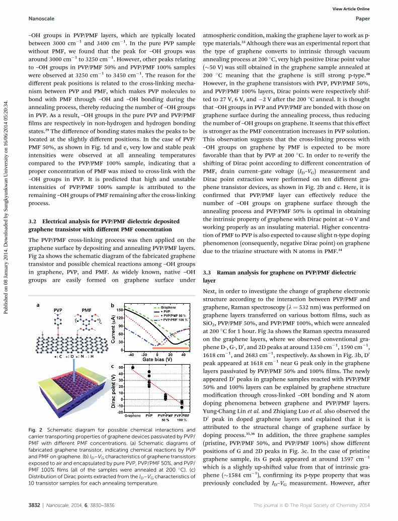
Next, in order to investigate the change of graphene electronicstructure according to the interaction between PVP/PMF andgraphene, Raman spectroscopy (l ¼ 532 nm) was performed ongraphene layers transferred on various bottom lms, such asSiO2, PVP/PMF 50%, and PVP/PMF 100%, which were annealedat 200 �C for 1 hour. Fig 3a shows the Raman spectra measuredon the graphene layers, where we observed conventional gra-phene D-, G-, D0, and 2D peaks at around 1350 cm�1, 1590 cm�1,1618 cm�1, and 2683 cm�1, respectively. As shown in Fig. 3b, D0
peak appeared at 1618 cm�1 near G peak only in the graphenelayers passivated by PVP/PMF 50% and 100% lms. The newlyappeared D0 peaks in graphene samples reacted with PVP/PMF50% and 100% layers can be explained by graphene structuremodication through cross-linked –OH bonding and N atomdoping phenomena between graphene and PVP/PMF layers.Yung-Chang Lin et al. and Zhiqiang Luo et al. also observed theD0 peak in doped graphene layers and explained that it isattributed to the structural change of graphene surface bydoping process.35,36 In addition, the three graphene samples(pristine, PVP/PMF 50%, and PVP/PMF 100%) show differentpositions of G and 2D peaks in Fig. 3c. In the case of pristinegraphene sample, its G peak appeared at around 1597 cm�1
which is a slightly up-shied value from that of intrinsic gra-phene (�1584 cm�1), conrming its p-type property that waspreviously concluded by ID–VG measurement. However, aer
This journal is © The Royal Society of Chemistry 2014
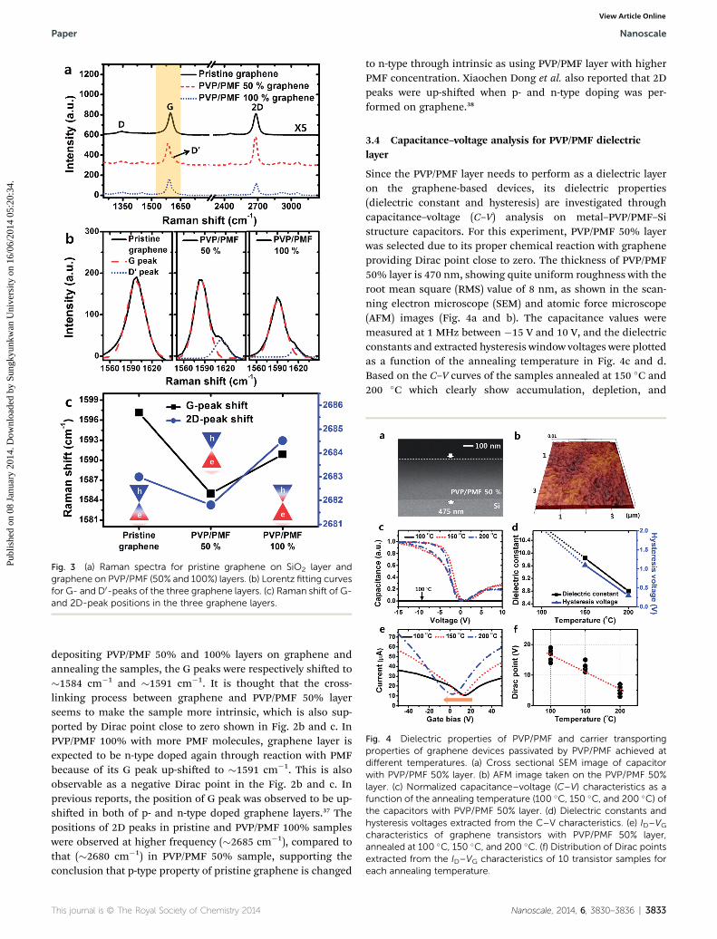
Fig. 3 (a) Raman spectra for pristine graphene on SiO2 layer andgraphene on PVP/PMF (50% and 100%) layers. (b) Lorentz fitting curvesfor G- and D0-peaks of the three graphene layers. (c) Raman shift of G-and 2D-peak positions in the three graphene layers.
Fig. 4 Dielectric properties of PVP/PMF and carrier transportingproperties of graphene devices passivated by PVP/PMF achieved atdifferent temperatures. (a) Cross sectional SEM image of capacitorwith PVP/PMF 50% layer. (b) AFM image taken on the PVP/PMF 50%layer. (c) Normalized capacitance–voltage (C–V) characteristics as afunction of the annealing temperature (100 �C, 150 �C, and 200 �C) ofthe capacitors with PVP/PMF 50% layer. (d) Dielectric constants andhysteresis voltages extracted from the C–V characteristics. (e) ID–VG
characteristics of graphene transistors with PVP/PMF 50% layer,annealed at 100 �C, 150 �C, and 200 �C. (f) Distribution of Dirac pointsextracted from the ID–VG characteristics of 10 transistor samples foreach annealing temperature.
Paper Nanoscale
Publ
ishe
d on
08
Janu
ary
2014
. Dow
nloa
ded
by S
ungk
yunk
wan
Uni
vers
ity o
n 16
/06/
2014
05:
20:3
4.
View Article Online
depositing PVP/PMF 50% and 100% layers on graphene andannealing the samples, the G peaks were respectively shied to�1584 cm�1 and �1591 cm�1. It is thought that the cross-linking process between graphene and PVP/PMF 50% layerseems to make the sample more intrinsic, which is also sup-ported by Dirac point close to zero shown in Fig. 2b and c. InPVP/PMF 100% with more PMF molecules, graphene layer isexpected to be n-type doped again through reaction with PMFbecause of its G peak up-shied to �1591 cm�1. This is alsoobservable as a negative Dirac point in the Fig. 2b and c. Inprevious reports, the position of G peak was observed to be up-shied in both of p- and n-type doped graphene layers.37 Thepositions of 2D peaks in pristine and PVP/PMF 100% sampleswere observed at higher frequency (�2685 cm�1), compared tothat (�2680 cm�1) in PVP/PMF 50% sample, supporting theconclusion that p-type property of pristine graphene is changed
This journal is © The Royal Society of Chemistry 2014
to n-type through intrinsic as using PVP/PMF layer with higherPMF concentration. Xiaochen Dong et al. also reported that 2Dpeaks were up-shied when p- and n-type doping was per-formed on graphene.38
3.4 Capacitance–voltage analysis for PVP/PMF dielectriclayer
Since the PVP/PMF layer needs to perform as a dielectric layeron the graphene-based devices, its dielectric properties(dielectric constant and hysteresis) are investigated throughcapacitance–voltage (C–V) analysis on metal–PVP/PMF–Sistructure capacitors. For this experiment, PVP/PMF 50% layerwas selected due to its proper chemical reaction with grapheneproviding Dirac point close to zero. The thickness of PVP/PMF50% layer is 470 nm, showing quite uniform roughness with theroot mean square (RMS) value of 8 nm, as shown in the scan-ning electron microscope (SEM) and atomic force microscope(AFM) images (Fig. 4a and b). The capacitance values weremeasured at 1 MHz between �15 V and 10 V, and the dielectricconstants and extracted hysteresis window voltages were plottedas a function of the annealing temperature in Fig. 4c and d.Based on the C–V curves of the samples annealed at 150 �C and200 �C which clearly show accumulation, depletion, and
Nanoscale, 2014, 6, 3830–3836 | 3833
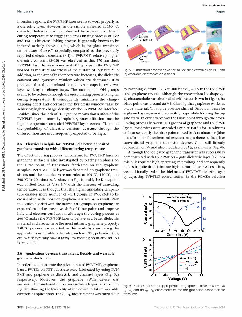
Fig. 5 Fabrication process flows for (a) flexible electronics on PET and(b) wearable electronics on a finger.
Fig. 6 Carrier transporting properties of graphene-based FWTEs. (a)ID–VG and (b) ID–VD characteristics for the graphene-based flexibletransistor.
Nanoscale Paper
Publ
ishe
d on
08
Janu
ary
2014
. Dow
nloa
ded
by S
ungk
yunk
wan
Uni
vers
ity o
n 16
/06/
2014
05:
20:3
4.
View Article Online
inversion regions, the PVP/PMF layer seems to work properly asa dielectric layer. However, in the sample annealed at 100 �C,dielectric behavior was not observed because of insufficientcuring temperature to trigger the cross-linking process of PVPand PMF. The cross-linking process is generally known to beinduced actively above 151 �C, which is the glass transitiontemperature of PVP.39 Especially, compared to the previouslyreported dielectric constant (�4) of PVP/PMF, relatively higherdielectric constant (8–10) was observed in this 470 nm thickPVP/PMF layer because non-cured –OH groups in the PVP/PMFworked as moisture absorbers at the surface of PVP lm.40 Inaddition, as the annealing temperature increases, the dielectricconstant and hysteresis window values are decreased. It ispredicted that this is related to the –OH groups in PVP/PMFlayer working as charge traps. The number of –OH groupsseems to be reduced through the cross-linking process at highercuring temperature. It consequently minimizes the charge-trapping effect and decreases the hysteresis window value byachieving higher charge density on the PVP/PMF-Si interface.Besides, since the lack of –OH groups means that surface of thePVP/PMF layer is more hydrophobic, water diffusion into thehigher temperature annealed PVP/PMF layer seems difficult andthe probability of dielectric constant decrease through thediffused moisture is consequently expected to be high.
3.5 Electrical analysis for PVP/PMF dielectric depositedgraphene transistor with different curing temperature
The effect of curing process temperature for PVP/PMF layer ongraphene surface is also investigated by placing emphasis onthe Dirac point of transistors fabricated on the graphenesamples. PVP/PMF 50% layer was deposited on graphene tran-sistors and the samples were annealed at 100 �C, 150 �C, and200 �C for 30 minutes. As shown in Fig. 4e and f, the Dirac pointwas shied from 16 V to 3 V with the increase of annealingtemperature. It is thought that the higher annealing tempera-ture enables more number of –OH groups in PVP/PMF to becross-linked with those on graphene surface. As a result, PMFmolecules bonded with the native –OH groups on graphene areexpected to induce negative shi of Dirac point and improvehole and electron conduction. Although the curing process at200 �C makes the PVP/PMF layer to behave as a better dielectricmaterial and also achieve the most intrinsic graphene property,150 �C process was selected in this work by considering theapplications on exible substrates such as PET, polyimide (PI),etc., which typically have a fairly low melting point around 150�C to 250 �C.
3.6 Application devices: transparent, exible and wearablegraphene electronics
In order to demonstrate the advantages of PVP/PMF, graphene-based FWTEs on PET substrate were fabricated by using PVP/PMF and graphene as dielectric and channel layers (Fig. 5a)respectively. Moreover, the graphene FWTE device wassuccessfully transferred onto a researcher's nger, as shown inFig. 5b, showing the feasibility of the device to future wearableelectronic applications. The ID–VGmeasurement was carried out
3834 | Nanoscale, 2014, 6, 3830–3836
by sweeping VG from�50 V to 100 V at VDS¼ 1 V in the PVP/PMF50% graphene FWTEs. Although the conventional V-shape ID–VG characteristic was obtained (dark line) as shown in Fig. 6a, itsDirac point was around 55 V indicating that graphene works asp-type material. This large positive shi of Dirac point can beexplained by re-generation of –OH groups while forming the topgate stack. In order to recover the Dirac point through the cross-linking process between –OH groups of graphene and PVP/PMFlayers, the devices were annealed again at 150 �C for 10 minutesand consequently the Dirac point moved back to about 1 V (blueline). In spite of the chemical reaction on graphene surface, likeconventional graphene transistor devices, ID is still linearlydependent on VD and also modulated by VG, as shown in Fig. 6b.
Although the top gated graphene transistor was successfullydemonstrated with PVP/PMF 50% gate dielectric layer (470 nmthick), it requires high operating gate voltage and consequentlymakes it difficult to fabricate high performance FWTEs. Thus,we additionally scaled the thickness of PVP/PMF dielectric layerby adjusting PVP/PMF concentration in the PGMEA solution
This journal is © The Royal Society of Chemistry 2014
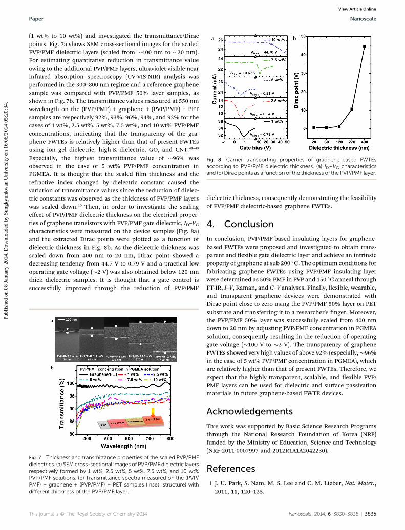
Fig. 8 Carrier transporting properties of graphene-based FWTEsaccording to PVP/PMF dielectric thickness. (a) ID–VG characteristicsand (b) Dirac points as a function of the thickness of the PVP/PMF layer.
Paper Nanoscale
Publ
ishe
d on
08
Janu
ary
2014
. Dow
nloa
ded
by S
ungk
yunk
wan
Uni
vers
ity o
n 16
/06/
2014
05:
20:3
4.
View Article Online
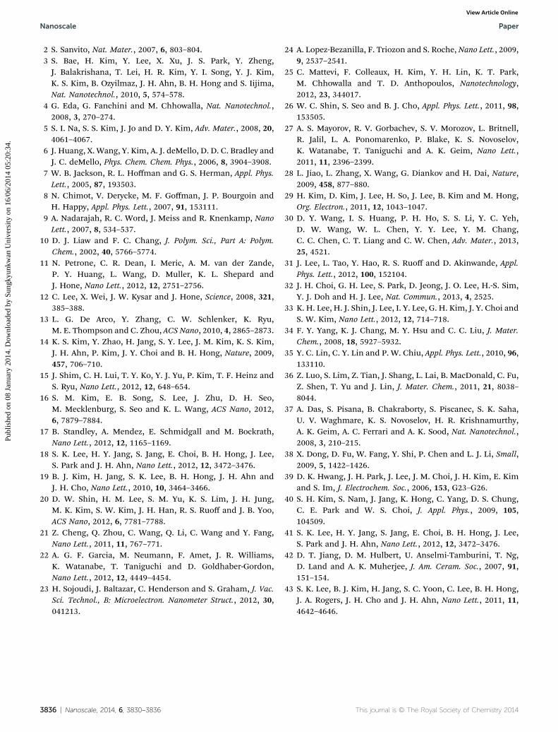
(1 wt% to 10 wt%) and investigated the transmittance/Diracpoints. Fig. 7a shows SEM cross-sectional images for the scaledPVP/PMF dielectric layers (scaled from �400 nm to �20 nm).For estimating quantitative reduction in transmittance valueowing to the additional PVP/PMF layers, ultraviolet-visible-nearinfrared absorption spectroscopy (UV-VIS-NIR) analysis wasperformed in the 300–800 nm regime and a reference graphenesample was compared with PVP/PMF 50% layer samples, asshown in Fig. 7b. The transmittance values measured at 550 nmwavelength on the (PVP/PMF) + graphene + (PVP/PMF) + PETsamples are respectively 92%, 93%, 96%, 94%, and 92% for thecases of 1 wt%, 2.5 wt%, 5 wt%, 7.5 wt%, and 10 wt% PVP/PMFconcentrations, indicating that the transparency of the gra-phene FWTEs is relatively higher than that of present FWTEsusing ion gel dielectric, high-K dielectric, GO, and CNT.41–43
Especially, the highest transmittance value of �96% wasobserved in the case of 5 wt% PVP/PMF concentration inPGMEA. It is thought that the scaled lm thickness and therefractive index changed by dielectric constant caused thevariation of transmittance values since the reduction of dielec-tric constants was observed as the thickness of PVP/PMF layerswas scaled down.40 Then, in order to investigate the scalingeffect of PVP/PMF dielectric thickness on the electrical proper-ties of graphene transistors with PVP/PMF gate dielectric, ID–VGcharacteristics were measured on the device samples (Fig. 8a)and the extracted Dirac points were plotted as a function ofdielectric thickness in Fig. 8b. As the dielectric thickness wasscaled down from 400 nm to 20 nm, Dirac point showed adecreasing tendency from 44.7 V to 0.79 V and a practical lowoperating gate voltage (�2 V) was also obtained below 120 nmthick dielectric samples. It is thought that a gate control issuccessfully improved through the reduction of PVP/PMF
Fig. 7 Thickness and transmittance properties of the scaled PVP/PMFdielectrics. (a) SEM cross-sectional images of PVP/PMF dielectric layersrespectively formed by 1 wt%, 2.5 wt%, 5 wt%, 7.5 wt%, and 10 wt%PVP/PMF solutions. (b) Transmittance spectra measured on the (PVP/PMF) + graphene + (PVP/PMF) + PET samples (Inset: structure) withdifferent thickness of the PVP/PMF layer.
This journal is © The Royal Society of Chemistry 2014
dielectric thickness, consequently demonstrating the feasibilityof PVP/PMF dielectric-based graphene FWTEs.
4. Conclusion
In conclusion, PVP/PMF-based insulating layers for graphene-based FWTEs were proposed and investigated to obtain trans-parent and exible gate dielectric layer and achieve an intrinsicproperty of graphene at sub 200 �C. The optimum conditions forfabricating graphene FWTEs using PVP/PMF insulating layerwere determined as 50% PMF in PVP and 150 �C anneal throughFT-IR, I–V, Raman, and C–V analyses. Finally, exible, wearable,and transparent graphene devices were demonstrated withDirac point close to zero using the PVP/PMF 50% layer on PETsubstrate and transferring it to a researcher's nger. Moreover,the PVP/PMF 50% layer was successfully scaled from 400 nmdown to 20 nm by adjusting PVP/PMF concentration in PGMEAsolution, consequently resulting in the reduction of operatinggate voltage (�100 V to �2 V). The transparency of grapheneFWTEs showed very high values of above 92% (especially,�96%in the case of 5 wt% PVP/PMF concentration in PGMEA), whichare relatively higher than that of present FWTEs. Therefore, weexpect that the highly transparent, scalable, and exible PVP/PMF layers can be used for dielectric and surface passivationmaterials in future graphene-based FWTE devices.
Acknowledgements
This work was supported by Basic Science Research Programsthrough the National Research Foundation of Korea (NRF)funded by the Ministry of Education, Science and Technology(NRF-2011-0007997 and 2012R1A1A2042230).
References
1 J. U. Park, S. Nam, M. S. Lee and C. M. Lieber, Nat. Mater.,2011, 11, 120–125.
Nanoscale, 2014, 6, 3830–3836 | 3835
Nanoscale Paper
Publ
ishe
d on
08
Janu
ary
2014
. Dow
nloa
ded
by S
ungk
yunk
wan
Uni
vers
ity o
n 16
/06/
2014
05:
20:3
4.
View Article Online
2 S. Sanvito, Nat. Mater., 2007, 6, 803–804.3 S. Bae, H. Kim, Y. Lee, X. Xu, J. S. Park, Y. Zheng,J. Balakrishana, T. Lei, H. R. Kim, Y. I. Song, Y. J. Kim,K. S. Kim, B. Ozyilmaz, J. H. Ahn, B. H. Hong and S. Iijima,Nat. Nanotechnol., 2010, 5, 574–578.
4 G. Eda, G. Fanchini and M. Chhowalla, Nat. Nanotechnol.,2008, 3, 270–274.
5 S. I. Na, S. S. Kim, J. Jo and D. Y. Kim, Adv. Mater., 2008, 20,4061–4067.
6 J. Huang, X. Wang, Y. Kim, A. J. deMello, D. D. C. Bradley andJ. C. deMello, Phys. Chem. Chem. Phys., 2006, 8, 3904–3908.
7 W. B. Jackson, R. L. Hoffman and G. S. Herman, Appl. Phys.Lett., 2005, 87, 193503.
8 N. Chimot, V. Derycke, M. F. Goffman, J. P. Bourgoin andH. Happy, Appl. Phys. Lett., 2007, 91, 153111.
9 A. Nadarajah, R. C. Word, J. Meiss and R. Knenkamp, NanoLett., 2007, 8, 534–537.
10 D. J. Liaw and F. C. Chang, J. Polym. Sci., Part A: Polym.Chem., 2002, 40, 5766–5774.
11 N. Petrone, C. R. Dean, I. Meric, A. M. van der Zande,P. Y. Huang, L. Wang, D. Muller, K. L. Shepard andJ. Hone, Nano Lett., 2012, 12, 2751–2756.
12 C. Lee, X. Wei, J. W. Kysar and J. Hone, Science, 2008, 321,385–388.
13 L. G. De Arco, Y. Zhang, C. W. Schlenker, K. Ryu,M. E. Thompson and C. Zhou, ACS Nano, 2010, 4, 2865–2873.
14 K. S. Kim, Y. Zhao, H. Jang, S. Y. Lee, J. M. Kim, K. S. Kim,J. H. Ahn, P. Kim, J. Y. Choi and B. H. Hong, Nature, 2009,457, 706–710.
15 J. Shim, C. H. Lui, T. Y. Ko, Y. J. Yu, P. Kim, T. F. Heinz andS. Ryu, Nano Lett., 2012, 12, 648–654.
16 S. M. Kim, E. B. Song, S. Lee, J. Zhu, D. H. Seo,M. Mecklenburg, S. Seo and K. L. Wang, ACS Nano, 2012,6, 7879–7884.
17 B. Standley, A. Mendez, E. Schmidgall and M. Bockrath,Nano Lett., 2012, 12, 1165–1169.
18 S. K. Lee, H. Y. Jang, S. Jang, E. Choi, B. H. Hong, J. Lee,S. Park and J. H. Ahn, Nano Lett., 2012, 12, 3472–3476.
19 B. J. Kim, H. Jang, S. K. Lee, B. H. Hong, J. H. Ahn andJ. H. Cho, Nano Lett., 2010, 10, 3464–3466.
20 D. W. Shin, H. M. Lee, S. M. Yu, K. S. Lim, J. H. Jung,M. K. Kim, S. W. Kim, J. H. Han, R. S. Ruoff and J. B. Yoo,ACS Nano, 2012, 6, 7781–7788.
21 Z. Cheng, Q. Zhou, C. Wang, Q. Li, C. Wang and Y. Fang,Nano Lett., 2011, 11, 767–771.
22 A. G. F. Garcia, M. Neumann, F. Amet, J. R. Williams,K. Watanabe, T. Taniguchi and D. Goldhaber-Gordon,Nano Lett., 2012, 12, 4449–4454.
23 H. Sojoudi, J. Baltazar, C. Henderson and S. Graham, J. Vac.Sci. Technol., B: Microelectron. Nanometer Struct., 2012, 30,041213.
3836 | Nanoscale, 2014, 6, 3830–3836
24 A. Lopez-Bezanilla, F. Triozon and S. Roche, Nano Lett., 2009,9, 2537–2541.
25 C. Mattevi, F. Colleaux, H. Kim, Y. H. Lin, K. T. Park,M. Chhowalla and T. D. Anthopoulos, Nanotechnology,2012, 23, 344017.
26 W. C. Shin, S. Seo and B. J. Cho, Appl. Phys. Lett., 2011, 98,153505.
27 A. S. Mayorov, R. V. Gorbachev, S. V. Morozov, L. Britnell,R. Jalil, L. A. Ponomarenko, P. Blake, K. S. Novoselov,K. Watanabe, T. Taniguchi and A. K. Geim, Nano Lett.,2011, 11, 2396–2399.
28 L. Jiao, L. Zhang, X. Wang, G. Diankov and H. Dai, Nature,2009, 458, 877–880.
29 H. Kim, D. Kim, J. Lee, H. So, J. Lee, B. Kim and M. Hong,Org. Electron., 2011, 12, 1043–1047.
30 D. Y. Wang, I. S. Huang, P. H. Ho, S. S. Li, Y. C. Yeh,D. W. Wang, W. L. Chen, Y. Y. Lee, Y. M. Chang,C. C. Chen, C. T. Liang and C. W. Chen, Adv. Mater., 2013,25, 4521.
31 J. Lee, L. Tao, Y. Hao, R. S. Ruoff and D. Akinwande, Appl.Phys. Lett., 2012, 100, 152104.
32 J. H. Choi, G. H. Lee, S. Park, D. Jeong, J. O. Lee, H.-S. Sim,Y. J. Doh and H. J. Lee, Nat. Commun., 2013, 4, 2525.
33 K. H. Lee, H. J. Shin, J. Lee, I. Y. Lee, G. H. Kim, J. Y. Choi andS. W. Kim, Nano Lett., 2012, 12, 714–718.
34 F. Y. Yang, K. J. Chang, M. Y. Hsu and C. C. Liu, J. Mater.Chem., 2008, 18, 5927–5932.
35 Y. C. Lin, C. Y. Lin and P. W. Chiu, Appl. Phys. Lett., 2010, 96,133110.
36 Z. Luo, S. Lim, Z. Tian, J. Shang, L. Lai, B. MacDonald, C. Fu,Z. Shen, T. Yu and J. Lin, J. Mater. Chem., 2011, 21, 8038–8044.
37 A. Das, S. Pisana, B. Chakraborty, S. Piscanec, S. K. Saha,U. V. Waghmare, K. S. Novoselov, H. R. Krishnamurthy,A. K. Geim, A. C. Ferrari and A. K. Sood, Nat. Nanotechnol.,2008, 3, 210–215.
38 X. Dong, D. Fu, W. Fang, Y. Shi, P. Chen and L. J. Li, Small,2009, 5, 1422–1426.
39 D. K. Hwang, J. H. Park, J. Lee, J. M. Choi, J. H. Kim, E. Kimand S. Im, J. Electrochem. Soc., 2006, 153, G23–G26.
40 S. H. Kim, S. Nam, J. Jang, K. Hong, C. Yang, D. S. Chung,C. E. Park and W. S. Choi, J. Appl. Phys., 2009, 105,104509.
41 S. K. Lee, H. Y. Jang, S. Jang, E. Choi, B. H. Hong, J. Lee,S. Park and J. H. Ahn, Nano Lett., 2012, 12, 3472–3476.
42 D. T. Jiang, D. M. Hulbert, U. Anselmi-Tamburini, T. Ng,D. Land and A. K. Muherjee, J. Am. Ceram. Soc., 2007, 91,151–154.
43 S. K. Lee, B. J. Kim, H. Jang, S. C. Yoon, C. Lee, B. H. Hong,J. A. Rogers, J. H. Cho and J. H. Ahn, Nano Lett., 2011, 11,4642–4646.
This journal is © The Royal Society of Chemistry 2014