polarization-induced transport in ferroelelctric
TRANSCRIPT
POLARIZATION-INDUCED TRANSPORT IN FERROELELCTRIC
ORGANIC FIELD-EFFECT TRANSISTORS
_______________________________________
A Dissertation
presented to
the Faculty of the Graduate School
at the University of Missouri-Columbia
_______________________________________________________
In Partial Fulfillment
of the Requirements for the Degree
Doctor of Philosophy
_____________________________________________________
by
AMRIT PRASAD LAUDARI
Dr. Suchi Guha, Dissertation Supervisor
MAY 2019
The undersigned, appointed by the dean of the Graduate School, have examined the dissertation
entitled
POLARIZATION-INDUCED TRANSPORT IN FERROELECTRIC ORGANIC FIELD-
EFFECT TRANSTISTORS
presented by Amrit Prasad Laudari,
a candidate for the degree of Doctor of Philosophy,
and hereby certify that, in their opinion, it is worthy of acceptance.
_____________________________________________________
Professor Suchi Guha
______________________________________________________
Professor Shubhra Gangopadhaya
_______________________________________________________
Professor Carsten Ullrich
________________________________________________________
Professor Guang Bian

This work is dedicated to its foundation; my country and my family.
ii
Acknowledgements
I express my sincere gratitude to my research adviser, Professor Suchi Guha. This
accomplishment is possible because of her exceptional motivation, support, and guidance.
Throughout the research, I found her as a shining example of what an adviser should be:
supportive, helpful, patient, generous, and always available. I am indebted to her for all she
has done for me. I am very grateful for her invaluable guidance to my success.
I am greatly thankful for the invaluable input from the members of my committee,
Professor Shubhra Gangopadhaya, Prof. Carsten Ullrich, and Professor Guang Bian. Their
excitement for research and insightful questions were tremendously helpful. I remain
grateful to Prof. Giovanni Vignale, Prof. Ping Yu and Prof. Paul Miceli for their time and
inputs.
My immeasurable gratitude goes to Prof. Kartik Ghosh from Missouri State
University, Springfield. His instruction has given me a fantastic foundation and his
mentoring and encouragement has always been far beyond what any one person deserves.
I further want to thank my collaborators Prof. John E Anthony at University of Kentucky,
Prof. Shadi Shahedipour-Sandvik at SUNY Polytechnic Institute, and Prof. Christopher
Arendse and Dr. Theophillus Muller at University of the Western Cape, South Africa.
I appreciate the generous funding of the National Science Foundation who made
this work possible. I also appreciate the wonderful support of my senior colleagues Danish
and Grant, and group members Soma and Alec, who were ever-ready to assist and share
useful information.
iii
Table of Contents
Acknowledgements ............................................................................................... ii
List of figures ....................................................................................................... vii
List of tables........................................................................................................ xix
Nomenclature ...................................................................................................... xx
Abstract ............................................................................................................. xxiii
1 Introduction ................................................................................................... 1
2 Organic FETs: materials, charge transport and working principle ........ 4
2.1 Organic semiconductors.............................................................................. 4
2.2 Charge transport in organic semiconductors............................................... 8
2.3 Dielectrics used in organic FETs .............................................................. 11
2.3.1 Ferroelectric dielectrics ..................................................................... 12
2.3.2 Non-polar (non-ferroelectric) dielectrics .......................................... 20
2.4 Working principle of organic FETs .......................................................... 22
3 Experimental methods ................................................................................ 32
3.1 Substrate preparation ................................................................................ 32
3.2 Thin film fabrication ................................................................................. 35
iv
3.2.1 Spin-coating ...................................................................................... 35
3.2.2 Drop casting ...................................................................................... 38
3.2.3 Inkjet printing.................................................................................... 41
3.2.4 Thermal evaporation ......................................................................... 42
3.3 Characterization ........................................................................................ 47
3.3.1 Surface morphology .......................................................................... 47
3.3.2 Electrical characterization ................................................................. 51
4 The role of Fröhlich polarons in pentacene FETs ................................... 56
4.1 Introduction ............................................................................................... 56
4.2 Comparison of polar versus non-polar dielectric ...................................... 58
4.3 Thickness-dependence of the ferroelectric layer ...................................... 62
4.4 Stacked PVDF-TrFE/inorganic layers ...................................................... 66
4.5 Raman scattering from pentacene on PVDF-TrFE ................................... 69
5 Transport properties in TIPS-pentacene FETs and diodes .................... 72
5.1 Charge transport models in disordered systems........................................ 72
5.1.1 Space-charge-limited-conduction (SCLC) and shallow traps ........... 76
5.2 Transport in two terminal devices............................................................. 77
5.3 Role of dielectrics in charge transport ...................................................... 80
5.4 Carrier transport in TIPS-pentacene FETs ................................................ 82
v
5.4.1 Temperature-dependent FET characteristics with non-ferroelectric
dielectrics .......................................................................................... 84
5.4.2 Temperature-dependent FET characteristics with PVDF-TrFE ....... 85
6 Dipole engineering of ferroelectric dielectrics- enhancement in FET
performance..................................................................................................... 92
6.1 Polarization rotation in the dielectric PVDF-TrFE ................................... 93
6.1.1 Introduction ....................................................................................... 93
6.1.2 Poling of PVDF-TrFE films.............................................................. 95
6.1.3 Small-molecule FETs with poled and unpoled PVDF-TrFE ............ 97
6.1.4 Capacitance-voltage characteristics of PVDF-TrFE metal-insulator-
metal capacitors .............................................................................. 105
6.1.5 Structure and morphology comparison at different poling conditions .
......................................................................................................... 108
6.2 Textured poling of dielectric PVDF-TrFE .............................................. 116
6.2.1 Technique used for textured poling of PVDF-TrFE and FET
performance .................................................................................... 116
6.2.2 Poling field optimization, microscopy and simulation ................... 122
7 Summary and suggested future works .................................................... 131
7.1 Summary ................................................................................................. 131
7.2 Suggested future works ........................................................................... 133
vi
7.2.1 Fast switching organic FETs by dipole engineering of PVDF-TrFE ...
......................................................................................................... 133
7.2.2 Carrier transport mechanism and FET mobility using non-linear
optics ............................................................................................... 134
7.2.3 Low operating organic FETs for sensing applications ................... 136
References .......................................................................................................... 138
Publications ....................................................................................................... 154
Vita ..................................................................................................................... 156
vii
List of figures
Figure 2.1 (a) Conjugated backbone and 2Pz orbitals pointing out of the molecular plane
(b) highest occupied molecular orbitals and lowest unoccupied molecular orbital. The red
arrows indicate the spin of electrons. .................................................................................. 5
Figure 2.2 (a) Molecular structure of pentacene (b) 3 × 3 nm2 STM images of pentacene
molecules adsorbed on a Ni(111) substrate at RT (1.49 nA and 1.8 mV. A molecular
model was also superimposed (adapted from reference [7]) .............................................. 6
Figure 2.3 Molecular structure of (a) dinaphtho[2,3-b:2',3'- f]thieno[3,2-b]thiophene
(DNTT), and (b)6,13-bis(triisopropylsilylethynyl)pentacene (TIPS-pentacene). .............. 7
Figure 2.4 (a) Optical image of thermally evaporated pentacene on top of patterned
Aluminum on a glass substrate. (b) Optical image of drop casted TIPS-pentacene on a
Si++/SiO2 substrate. ............................................................................................................ 8
Figure 2.5 (a) Variation of charge with voltage in polar dielectric. (b) Dipoles in polar
dielectric, arrow shows the direction of polarization. (c) Variation of polarization with an
applied field in a polar dielectric. ..................................................................................... 12
Figure 2.6 Molecular structure of PVDF-TrFE . ............................................................. 13
Figure 2.7 Chemical structures of (a) α PVDF and (b) β PVDF. .................................... 14
Figure 2.8 (a) Chemical structure of β PVDF-TrFE. (b) Raman spectrum of a PVDF-
TrFE film. (c) FTIR spectrum of a PVDF-TrFE films. .................................................... 15
Figure 2.9 (a) Polarization versus voltage measurement of PVDF-TrFE film using a
Sawyer-Tower circuit. (b) SEM image of as casted thin film of PVDF-TrFE. ................ 15
Figure 2.10 Schematics for SHG experimental set up transmission geometry. ............... 17
viii
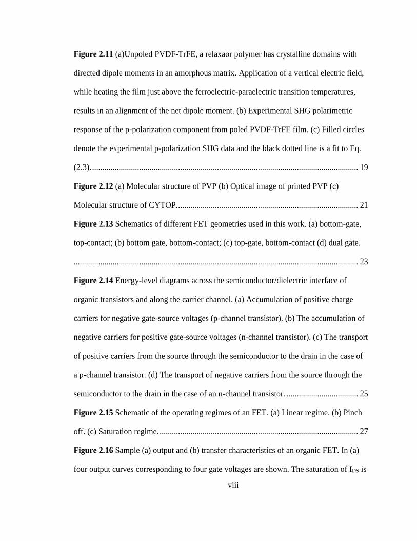
Figure 2.11 (a)Unpoled PVDF-TrFE, a relaxaor polymer has crystalline domains with
directed dipole moments in an amorphous matrix. Application of a vertical electric field,
while heating the film just above the ferroelectric-paraelectric transition temperatures,
results in an alignment of the net dipole moment. (b) Experimental SHG polarimetric
response of the p-polarization component from poled PVDF-TrFE film. (c) Filled circles
denote the experimental p-polarization SHG data and the black dotted line is a fit to Eq.
(2.3). .................................................................................................................................. 19
Figure 2.12 (a) Molecular structure of PVP (b) Optical image of printed PVP (c)
Molecular structure of CYTOP. ........................................................................................ 21
Figure 2.13 Schematics of different FET geometries used in this work. (a) bottom-gate,
top-contact; (b) bottom gate, bottom-contact; (c) top-gate, bottom-contact (d) dual gate.
........................................................................................................................................... 23
Figure 2.14 Energy-level diagrams across the semiconductor/dielectric interface of
organic transistors and along the carrier channel. (a) Accumulation of positive charge
carriers for negative gate-source voltages (p-channel transistor). (b) The accumulation of
negative carriers for positive gate-source voltages (n-channel transistor). (c) The transport
of positive carriers from the source through the semiconductor to the drain in the case of
a p-channel transistor. (d) The transport of negative carriers from the source through the
semiconductor to the drain in the case of an n-channel transistor. ................................... 25
Figure 2.15 Schematic of the operating regimes of an FET. (a) Linear regime. (b) Pinch
off. (c) Saturation regime. ................................................................................................. 27
Figure 2.16 Sample (a) output and (b) transfer characteristics of an organic FET. In (a)
four output curves corresponding to four gate voltages are shown. The saturation of IDS is
ix
clearly seen in each of the curves. In (b) both the IDS and the square root of IDS are
plotted. IDS is plotted on a logarithm scale to better show the switching behavior of the
FET. The linear behavior of the square root of IDS is also clearly seen. ........................... 30
Figure 3.1 (a) Schematics of drop casting method (b) drop casted thin film of TIPS-
pentacene........................................................................................................................... 39
Figure3.2 (a) SEM image of spin coated TIPS-pentacene. (b) Transfer from spin coated
TIPS-pentacene FET. (c) SEM image of drop cased TIPS-pentacene. (d) Transfer from
drop casted TIPS-pentacene FET. Channel length of both FETs was 50 µm. ................. 40
Figure 3.3 (a) The jetting waveform used for printing PVP. (b) Drop watcher image of
ejection of PVP solution. .................................................................................................. 42
Figure 3.4 Picture of (a) inside thermal evaporation chamber (b) MBraun glove box with
thermal evaporator in left box and spin coater in right box. ............................................. 44
Figure 3.5 Sample mask design used for patterning top contacts for organic FETs and
capacitors. (a) Gate electrode. (b) Source drain electrodes. (c) Optical images of FETs
and capacitor devices. ....................................................................................................... 46
Figure 3.6 (a) AFM images from drop casted TIPS-pentacene (b) Spin-coated PVDF-
TrFE .................................................................................................................................. 48
Figure 3.7 SEM images from spin coated PVDF-TrFE on aluminum coated glass with (a)
1 kV (b) 5 kV accelerating voltage. .................................................................................. 50
Figure 3.8 Three test liquid drops on the surface of printed PVP (a) water (b) formamide
(c) diiodomethane. ............................................................................................................ 51
x
Figure 3.9 (a) MIS Capacitance-Voltage from Al/PVDF-TrFE/pentacene/Au structure
(b) MIM Capacitance-frequency characteristics from Al/PVDF-TrFE/Al structure (c)
dissipation factor from Al/PVDF-TrFE/Al structure. ....................................................... 53
Figure 3.10 Photograph of (a) sample on the stage inside the cryostat (b) Modified
closed-cycle helium cryostat (APD Cryogenics). ............................................................. 55
Figure 4.1 Schematic of a ferroelectric-based FET where the dynamic coupling of charge
carriers to the electronic polarization at the semiconductor-dielectric interface is
illustrated. In addition to the bulk disorder within the semiconductor, there is trapping of
charges at the interface. ..................................................................................................... 58
Figure 4.2 (a) Transfer curves at different temperatures from 100K to 350K for a
pentacene FET with PMMA as the dielectric layer. (b) Transfer curves at different
temperatures from 200K to 440K for a pentacene FET with PVDF-TrFE as the dielectric
layer. In both cases, VDS=-4V. .......................................................................................... 59
Figure 4.3 Variation of threshold voltage with temperature (a) PMMA FET and (b)
PVDF-TrFE TET. ............................................................................................................. 60
Figure 4.4 Comparison of the charge carrier mobility as a function of temperature in
pentacene FETs using PMMA and PVDF-TrFE as dielectric layers. The dielectric
constant of PVDF-TrFE as a function of temperature shown in the figure is from Ref. 42.
........................................................................................................................................... 61
Figure 4.5 Arrhenius plots of FET mobilities in the ferroelectric phase for varying
thicknesses of the PVDF-TrFE layer. ............................................................................... 64
xi
Figure 4.6 (a) Comparison of the trapped charge density of the PMMA-based pentacene
OFET with a PVDF-TrFE-based OFET. (b) The trapped charge density as a function of
temperature for the 20nm, 90nm, and 130nm thick PVDF-TrFE devices. ....................... 65
Figure 4.7 Comparison of single layer PVDF-TrFE and stacked PVDF-TrFE/ SiO2
OFETs with (a) 20nm, (b) 90nm, and (c) 500nm, of the PVDF-TrFE thickness. ............ 66
Figure 4.8 Temperature-dependent mobility of Fröhlich polarons for pentacene FETs
with three thicknesses of the PVDF-TrFE layer. The bold line is a fit to the model
discussed in the text. ......................................................................................................... 68
Figure 4.9 Raman spectra of pentacene on PVDF-TrFE as a function of temperature. .. 70
Figure 5.1 (a) Schematic of DOS for a crystalline and an amorphous semiconductor. The
mobility edges in an amorphous semiconductor play a similar role as the band edges in a
crystal. (b) Schematic of trap states. (c) Schematic of discrete trap space-charge-limited
conduction in a log-log plot of current density (J) versus voltage. ................................... 73
Figure 5.2 (a) J-V characteristics (log-log plot) of pentacene at 300 K. The inset shows
the J-V behavior at different temperatures. The chemical structure of a pentacene
molecule is shown in the inset. (b) Product of the trapping fraction and carrier mobility as
a function of temperature for a pentacene diode. (Inset) Schematic of the energy levels. 78
Figure 5.3 (a) Chemical structure of TIPS-pentacene and an optical image from a TIPS-
pentacene device. (b) and (c) J-V curves from a TIPS-pentacene two-terminal device as a
function of temperature. (d) J-V curve (log-log plot) at 300 K showing all four regions,
characteristics of discrete trap SCLC. Inset shows the bulk carrier mobilities as a function
of temperature. .................................................................................................................. 79
xii
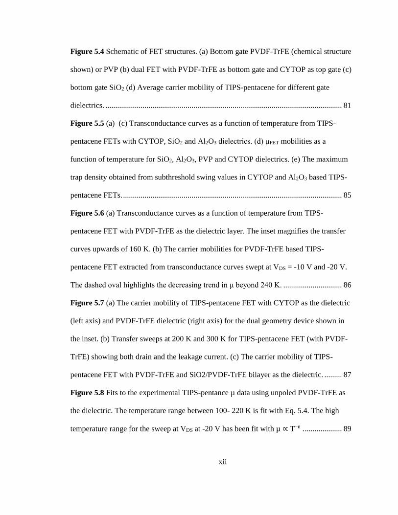
Figure 5.4 Schematic of FET structures. (a) Bottom gate PVDF-TrFE (chemical structure
shown) or PVP (b) dual FET with PVDF-TrFE as bottom gate and CYTOP as top gate (c)
bottom gate SiO2 (d) Average carrier mobility of TIPS-pentacene for different gate
dielectrics. ......................................................................................................................... 81
Figure 5.5 (a)–(c) Transconductance curves as a function of temperature from TIPS-
pentacene FETs with CYTOP, SiO2 and Al2O3 dielectrics. (d) μFET mobilities as a
function of temperature for SiO2, Al2O3, PVP and CYTOP dielectrics. (e) The maximum
trap density obtained from subthreshold swing values in CYTOP and Al2O3 based TIPS-
pentacene FETs. ................................................................................................................ 85
Figure 5.6 (a) Transconductance curves as a function of temperature from TIPS-
pentacene FET with PVDF-TrFE as the dielectric layer. The inset magnifies the transfer
curves upwards of 160 K. (b) The carrier mobilities for PVDF-TrFE based TIPS-
pentacene FET extracted from transconductance curves swept at VDS = -10 V and -20 V.
The dashed oval highlights the decreasing trend in μ beyond 240 K. .............................. 86
Figure 5.7 (a) The carrier mobility of TIPS-pentacene FET with CYTOP as the dielectric
(left axis) and PVDF-TrFE dielectric (right axis) for the dual geometry device shown in
the inset. (b) Transfer sweeps at 200 K and 300 K for TIPS-pentacene FET (with PVDF-
TrFE) showing both drain and the leakage current. (c) The carrier mobility of TIPS-
pentacene FET with PVDF-TrFE and SiO2/PVDF-TrFE bilayer as the dielectric. ......... 87
Figure 5.8 Fits to the experimental TIPS-pentance µ data using unpoled PVDF-TrFE as
the dielectric. The temperature range between 100- 220 K is fit with Eq. 5.4. The high
temperature range for the sweep at VDS at -20 V has been fit with µ ∝ T−n . ................... 89
xiii
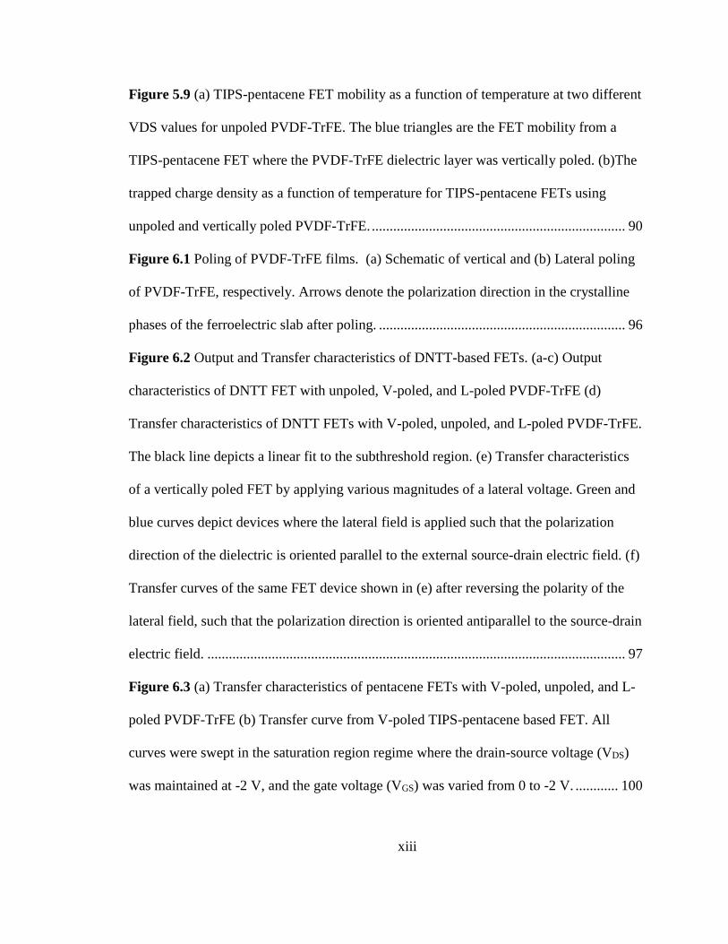
Figure 5.9 (a) TIPS-pentacene FET mobility as a function of temperature at two different
VDS values for unpoled PVDF-TrFE. The blue triangles are the FET mobility from a
TIPS-pentacene FET where the PVDF-TrFE dielectric layer was vertically poled. (b)The
trapped charge density as a function of temperature for TIPS-pentacene FETs using
unpoled and vertically poled PVDF-TrFE. ....................................................................... 90
Figure 6.1 Poling of PVDF-TrFE films. (a) Schematic of vertical and (b) Lateral poling
of PVDF-TrFE, respectively. Arrows denote the polarization direction in the crystalline
phases of the ferroelectric slab after poling. ..................................................................... 96
Figure 6.2 Output and Transfer characteristics of DNTT-based FETs. (a-c) Output
characteristics of DNTT FET with unpoled, V-poled, and L-poled PVDF-TrFE (d)
Transfer characteristics of DNTT FETs with V-poled, unpoled, and L-poled PVDF-TrFE.
The black line depicts a linear fit to the subthreshold region. (e) Transfer characteristics
of a vertically poled FET by applying various magnitudes of a lateral voltage. Green and
blue curves depict devices where the lateral field is applied such that the polarization
direction of the dielectric is oriented parallel to the external source-drain electric field. (f)
Transfer curves of the same FET device shown in (e) after reversing the polarity of the
lateral field, such that the polarization direction is oriented antiparallel to the source-drain
electric field. ..................................................................................................................... 97
Figure 6.3 (a) Transfer characteristics of pentacene FETs with V-poled, unpoled, and L-
poled PVDF-TrFE (b) Transfer curve from V-poled TIPS-pentacene based FET. All
curves were swept in the saturation region regime where the drain-source voltage (VDS)
was maintained at -2 V, and the gate voltage (VGS) was varied from 0 to -2 V. ............ 100
xiv
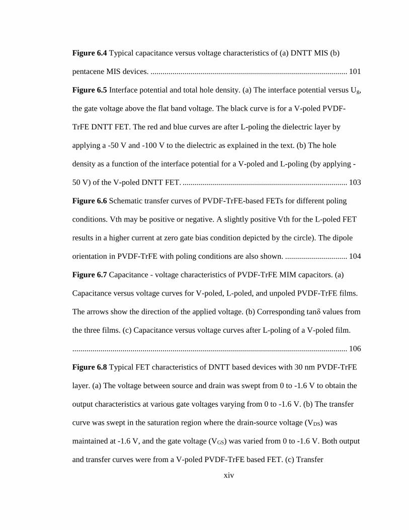
Figure 6.4 Typical capacitance versus voltage characteristics of (a) DNTT MIS (b)
pentacene MIS devices. .................................................................................................. 101
Figure 6.5 Interface potential and total hole density. (a) The interface potential versus Ug,
the gate voltage above the flat band voltage. The black curve is for a V-poled PVDF-
TrFE DNTT FET. The red and blue curves are after L-poling the dielectric layer by
applying a -50 V and -100 V to the dielectric as explained in the text. (b) The hole
density as a function of the interface potential for a V-poled and L-poling (by applying -
50 V) of the V-poled DNTT FET. .................................................................................. 103
Figure 6.6 Schematic transfer curves of PVDF-TrFE-based FETs for different poling
conditions. Vth may be positive or negative. A slightly positive Vth for the L-poled FET
results in a higher current at zero gate bias condition depicted by the circle). The dipole
orientation in PVDF-TrFE with poling conditions are also shown. ............................... 104
Figure 6.7 Capacitance - voltage characteristics of PVDF-TrFE MIM capacitors. (a)
Capacitance versus voltage curves for V-poled, L-poled, and unpoled PVDF-TrFE films.
The arrows show the direction of the applied voltage. (b) Corresponding tanδ values from
the three films. (c) Capacitance versus voltage curves after L-poling of a V-poled film.
......................................................................................................................................... 106
Figure 6.8 Typical FET characteristics of DNTT based devices with 30 nm PVDF-TrFE
layer. (a) The voltage between source and drain was swept from 0 to -1.6 V to obtain the
output characteristics at various gate voltages varying from 0 to -1.6 V. (b) The transfer
curve was swept in the saturation region where the drain-source voltage (VDS) was
maintained at -1.6 V, and the gate voltage (VGS) was varied from 0 to -1.6 V. Both output
and transfer curves were from a V-poled PVDF-TrFE based FET. (c) Transfer
xv
characteristics of a V-poled FET after applying two different lateral electric fields. The
lateral field was applied such that the polarization direction of the dielectric is oriented
parallel to the external source-drain electric field. .......................................................... 107
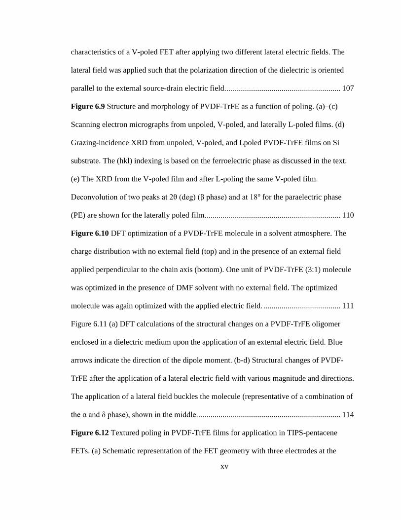
Figure 6.9 Structure and morphology of PVDF-TrFE as a function of poling. (a)–(c)
Scanning electron micrographs from unpoled, V-poled, and laterally L-poled films. (d)
Grazing-incidence XRD from unpoled, V-poled, and Lpoled PVDF-TrFE films on Si
substrate. The (hkl) indexing is based on the ferroelectric phase as discussed in the text.
(e) The XRD from the V-poled film and after L-poling the same V-poled film.
Deconvolution of two peaks at 2θ (deg) (β phase) and at 18o for the paraelectric phase
(PE) are shown for the laterally poled film. .................................................................... 110
Figure 6.10 DFT optimization of a PVDF-TrFE molecule in a solvent atmosphere. The
charge distribution with no external field (top) and in the presence of an external field
applied perpendicular to the chain axis (bottom). One unit of PVDF-TrFE (3:1) molecule
was optimized in the presence of DMF solvent with no external field. The optimized
molecule was again optimized with the applied electric field. ....................................... 111
Figure 6.11 (a) DFT calculations of the structural changes on a PVDF-TrFE oligomer
enclosed in a dielectric medium upon the application of an external electric field. Blue
arrows indicate the direction of the dipole moment. (b-d) Structural changes of PVDF-
TrFE after the application of a lateral electric field with various magnitude and directions.
The application of a lateral field buckles the molecule (representative of a combination of
the α and δ phase), shown in the middle. ........................................................................ 114
Figure 6.12 Textured poling in PVDF-TrFE films for application in TIPS-pentacene
FETs. (a) Schematic representation of the FET geometry with three electrodes at the
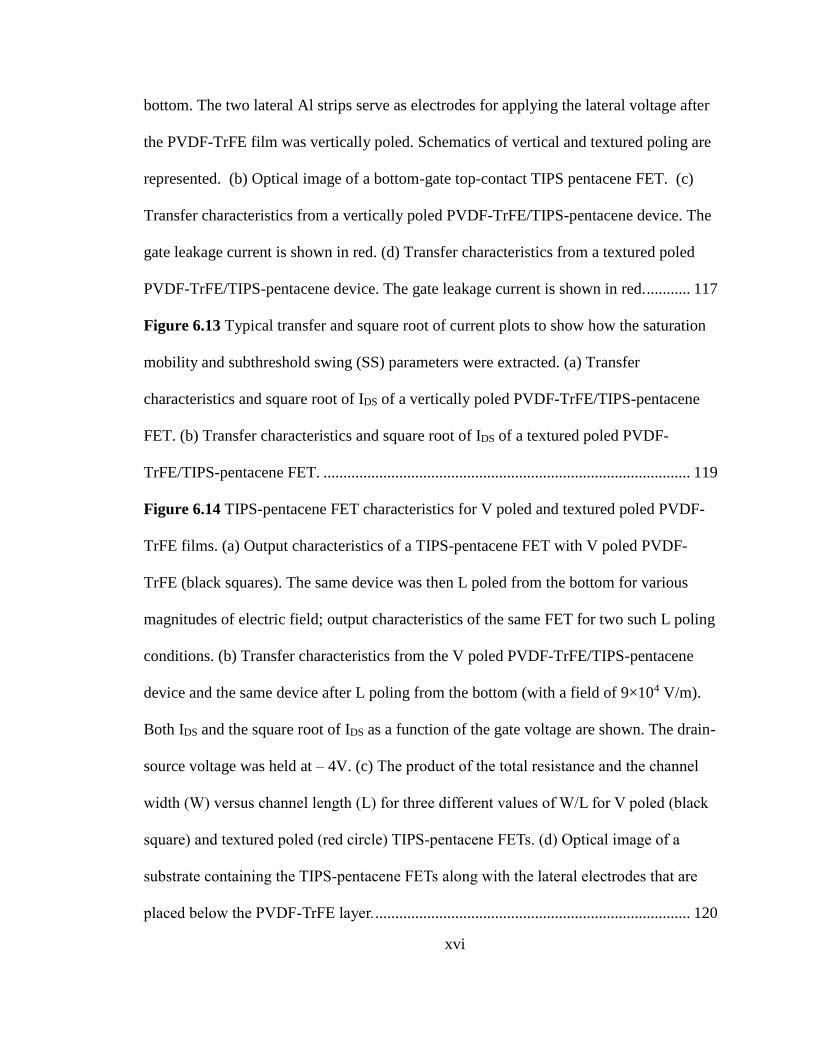
xvi
bottom. The two lateral Al strips serve as electrodes for applying the lateral voltage after
the PVDF-TrFE film was vertically poled. Schematics of vertical and textured poling are
represented. (b) Optical image of a bottom-gate top-contact TIPS pentacene FET. (c)
Transfer characteristics from a vertically poled PVDF-TrFE/TIPS-pentacene device. The
gate leakage current is shown in red. (d) Transfer characteristics from a textured poled
PVDF-TrFE/TIPS-pentacene device. The gate leakage current is shown in red. ........... 117
Figure 6.13 Typical transfer and square root of current plots to show how the saturation
mobility and subthreshold swing (SS) parameters were extracted. (a) Transfer
characteristics and square root of IDS of a vertically poled PVDF-TrFE/TIPS-pentacene
FET. (b) Transfer characteristics and square root of IDS of a textured poled PVDF-
TrFE/TIPS-pentacene FET. ............................................................................................ 119
Figure 6.14 TIPS-pentacene FET characteristics for V poled and textured poled PVDF-
TrFE films. (a) Output characteristics of a TIPS-pentacene FET with V poled PVDF-
TrFE (black squares). The same device was then L poled from the bottom for various
magnitudes of electric field; output characteristics of the same FET for two such L poling
conditions. (b) Transfer characteristics from the V poled PVDF-TrFE/TIPS-pentacene
device and the same device after L poling from the bottom (with a field of 9×10⁴ V/m).
Both IDS and the square root of IDS as a function of the gate voltage are shown. The drain-
source voltage was held at – 4V. (c) The product of the total resistance and the channel
width (W) versus channel length (L) for three different values of W/L for V poled (black
square) and textured poled (red circle) TIPS-pentacene FETs. (d) Optical image of a
substrate containing the TIPS-pentacene FETs along with the lateral electrodes that are
placed below the PVDF-TrFE layer. ............................................................................... 120
xvii
Figure 6.15 Transfer characteristics of TIPS-pentacene FETs with different poling
conditions of the PVDF-TrFE layer and surface morphology. (a) Transfer characteristics
of a V-poled PVDF-TrFE layer (black) and the transfer curve for the same device after L-
poling (from the bottom) using an electric field of 105 V/m (red). (b) Transfer curve of a
V-poled FET (black) and after L-poling the same device from the top with an electric
field of 6×10³ V/m (red). (c) SEM image of a V-poled PVDF-TrFE film. (d) AFM image
of a V poled PVDF-TrFE film. (e) AFM image of a V-poled PVDF-TrFE film, which
was L-poled from the top with an electric field of 6×10³ V/m. ...................................... 123
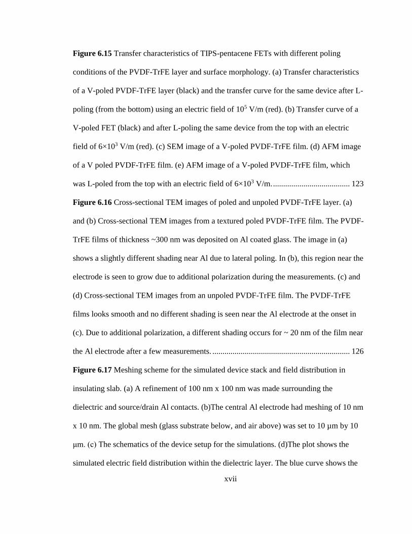
Figure 6.16 Cross-sectional TEM images of poled and unpoled PVDF-TrFE layer. (a)
and (b) Cross-sectional TEM images from a textured poled PVDF-TrFE film. The PVDF-
TrFE films of thickness ~300 nm was deposited on Al coated glass. The image in (a)
shows a slightly different shading near Al due to lateral poling. In (b), this region near the
electrode is seen to grow due to additional polarization during the measurements. (c) and
(d) Cross-sectional TEM images from an unpoled PVDF-TrFE film. The PVDF-TrFE
films looks smooth and no different shading is seen near the Al electrode at the onset in
(c). Due to additional polarization, a different shading occurs for ~ 20 nm of the film near
the Al electrode after a few measurements. .................................................................... 126
Figure 6.17 Meshing scheme for the simulated device stack and field distribution in
insulating slab. (a) A refinement of 100 nm x 100 nm was made surrounding the
dielectric and source/drain Al contacts. (b)The central Al electrode had meshing of 10 nm
x 10 nm. The global mesh (glass substrate below, and air above) was set to 10 µm by 10
μm. (c) The schematics of the device setup for the simulations. (d)The plot shows the
simulated electric field distribution within the dielectric layer. The blue curve shows the
xviii
field distribution as seen within the dielectric slab. The inset shows the region of interest,
namely, the field distribution in the dielectric layer just above the middle (gate) electrode.
......................................................................................................................................... 128
Figure 7.1 (a) FET design as a sensor and (b) a photograph of such device based on
pentacene FET ................................................................................................................ 136
xix
List of tables
Table 2-I Dielectric constant of dielectrics used in this research. ................................... 22
Table 3-I Recipes used for spin coating of major polymers used in this work. ............... 37
Table 4-I The polaron hopping barrier and hopping lengths obtained by fits to Eq. (4.5).
........................................................................................................................................... 69
Table 6-I The FET parameters extracted from unpoled V-poled, and L-poled PVDF-
TrFE from DNTT and pentacene FETs. ........................................................................... 99
Table 6-II FET parameters for a vertically poled PVDF-TrFE film using DNTT as the
organic semiconductor. Lateral electric field is applied in the direction of EDS, and then
the polarity is reversed. ................................................................................................... 102
Table 6-III Dipole moment of a PVDF-TrFE (in a solvent bath) upon application of an
external electric field in the lateral direction. ................................................................. 112
Table 6-IV Dipole moment of a PVDF-TrFE (in a solvent bath) upon application of an
external electric field in the perpendicular direction. ..................................................... 113
xx
Nomenclature
FET – field-effect transistor
MIS – metal-insulator-semiconductor
MIM – metal-insulator-metal
AFM – atomic force microscope
SEM – scanning electron microscope
XRD – x-ray diffraction
C-V – capacitance-voltage
G-V – conductance-voltage
C-f – capacitance-frequency
I-V – current-voltage
VGS – gate voltage
VDS – drain-source voltage
VTh – threshold voltage
ΔVTh – threshold voltage shift
IDS– drain-source current
xxi
μsat – saturation charge carrier mobility
Ion/Ioff – current on/off ratio
W/L – width/length of the drain-source channel
Pr – remnant polarization
Ps – saturation polarization
HOMO – highest occupied molecular orbital
LUMO – lowest unoccupied molecular orbital
PVDF – polyvinylidene fluoride
PVDF-TrFE – polyvinylidene fluoride-trifluoroethylene
PVP – poly-4-vinyl phenol
PGMEA – propylene glycol monomethyl ether acetate
PMMA – polymethyl methacrylate
SiO2 – silicon dioxide
DNTT – dinaphtho[2,3-b:2',3'-f]thieno[3,2-b]thiophene
TIPS-pentacene – 6,13-bis(triisopropylsilylethynyl)pentacene
DMSO – dimethyl sulfoxide
xxii
DMF – dimethyl formamide
wt% - weight percent (measure of solution concentration)
CCD – charge-coupled device
TRM-SHG – time-resolved microscopic optical second harmonic generation
EFISHG – Electric field-induced second-harmonic generation
xxiii
Abstract
In this research we study the role of ferroelectric dielectrics in organic field-effect
transistors (FETs) to understand the mechanism of charge transport in organic
semiconductors. The ferroelectric nature of the polymer, poly(vinylidene fluoride)
(PVDF)), has been known for over 45 years. However, its role in interfacial transport in
organic/polymeric FETs is not that well understood. PVDF and its copolymer,
polyvinylidene fluoride-trifluoroethylene (PVDF-TrFE), as a dielectric in organic FETs is
a perfect test-bed for conducting transport studies where a systematic tuning of the
dielectric constant with temperature may be achieved. By choosing small molecule organic
semiconductors - pentacene and 6,13 bis(triisopropylsilylethynyl)pentacene (TIPS-
pentacene) – along with a copolymer PVDF-TrFE as the dielectric layer, the FET
characteristics are monitored as a function of temperature. Pentacene FETs show a weak
temperature dependence of the charge carrier mobility in the ferroelectric phase of PVDF-
TrFE, which is attributed to polarization fluctuation driven transport resulting from a
coupling of the charge carriers to the surface phonons of the dielectric layer. A negative
coefficient of carrier mobility is observed in TIPS-pentacene upwards of 200 K with the
ferroelectric dielectric, while an activated transport is observed with non-ferroelectric
dielectrics. We show that this behavior is correlated with the nature of the trap states in
TIPS-pentacene.
We also developed the method of dipole engineering of the PVDF-TrFE films to
enhance the properties of organic FETs. PVDF-TrFE, despite its applications in a vast
range of work (including as a gate dielectric in organic FET and sensing applications) poses
xxiv
concerns such as higher conductivity compared to other polymer non-ferroelectric
dielectrics. We have come up with new methods of electrical poling the dielectric layer to
enhance FET performance as well as reduce gate leakage issues. We demonstrate the effect
of polarization rotation in PVDF-TrFE on the performance of small-molecule-based
organic FETs. The subthreshold swing and other transistor parameters in organic FETs can
be controlled in a reversible fashion by switching the polarization direction in the PVDF-
TrFE layer. We further demonstrate a novel method of selective poling of the dielectric
layer. By using solution processed TIPS-pentacene as the organic semiconductor, it is
shown that textured poling of the PVDF-TrFE layer dramatically improves FET properties
compared to unpoled or uniformly poled ferroelectric films. The texturing is achieved by
first vertically poling the PVDF-TrFE film and then laterally poling the dielectric layer
close to the gate electrode. TIPS-pentacene FETs show on/off ratios of 105 and hole
mobilities of 1 cm2/Vs under ambient conditions with operating voltages well below -4 V.
This research opens prospects of achieving low-operating FETs without any expensive
patterning techniques.
Keywords: Organic semiconductor, organic field-effect transistor, polymer ferroelectric,
charge transport, band-like transport, Fröhlich polaron, polarization rotation, poling
1
1 Introduction
Organic electronics is a field of electronics which utilizes conducting polymers and
molecules. The field of organic electronics has grown significantly after the discovery of
the first highly conductive polymer – polyacetylene -in 1977, by A. J. Heeger, H.
Shirakawa, and Alan G. MacDiamid (Nobel Prize in Chemistry in 2000).1 One of the most
significant milestones in organic semiconductors was the realization of organic field effect
transistors (FETs) by a polythiophene transistor by Tsumora et al. in 1986.2 The building
blocks of organic semiconductors are mainly carbon and hydrogen atoms. Some orbitals
hybridize (forming covalent bonds between carbon atoms) while other orbitals remain
unhybridized.3 Overlapping of adjacent unhybridized orbitals results in shared molecular
orbitals and this is responsible for carrier transport and semiconducting properties in these
materials. Some examples of organic electronic devices are organic FETs, light emitting
diodes (LEDs), solar cells and photodetectors.
The research activities in organic devices are flourishing due to their promise in
large-area electronics fabricated on flexible substrates using low-cost and unconventional
means such as spin coating, room temperature printing, and roll-to-roll processing making
them attractive for an ever-growing range of technological applications. Interestingly,
some organic FETs have shown performances better than amorphous silicon thin film
transistors and are already utilized in the market of displays such as in OLED TVs by
LG.Inc. While much work has been done in the field of organic semiconductors, the field
is still new compared to the research and understanding of traditional electronics based on
inorganic semiconductors. Thus, further work is required before realizing the full potential
2
of organic electronics and their applications. Many fundamental aspects of charge carrier
transport in an organic semiconductor are not fully understood yet.
In this research, we fabricate and characterize organic FETs using several organic
semiconductors and polymer dielectrics. We also use conventional oxide-based dielectrics
for a comparative study. One main objective of this research is to study the role of polar
dielectrics in organic FETs to understand the mechanism of charge transport in organic
semiconductors. The second objective of this research is to develop dipole engineering
techniques in polar dielectrics to enhance the FET properties.
In chapter 2, we begin with a brief introduction of organic semiconductors and
polymer dielectrics including ferroelectric co-polymer poly(vinylidene fluoride-co-
trifluoroethylene) (PVDF-TrFE), the main dielectric used in this work. This chapter also
contains a brief description of the mechanism of ferroelectricity in PVDF-TrFE and some
results for its phase conformation which has been employed in this report. Chapter 2 also
introduces organic FETs and the geometry of organic FETs used in this work. Chapter 3
explores the experimental methods employed in this work which contains three sections;
substrate preparation, device fabrication, and characterization. The device fabrication part
gives an overview of thin film deposition techniques for organic devices whereas the
characterization section discusses concise descriptions of employed device
characterization techniques. Chapter 4 marks the beginning of experimental results. In that
chapter we discuss the role of Fröhlich polarons in pentacene based organic FETs. It
includes a detailed temperature dependent electrical characterization of organic FETs with
various thicknesses of PVDF-TrFE dielectric and stacked dielectric layers to decouple the
3
role of Fröhlich polarons from the short-range Holstein polarons. Chapter 5 is a discussion
on the general mechanism of transport involving traps using solution-processed organic
semiconductor, 6,13 bis(triisopropylsilylethynyl)pentacene (TIPS-pentacene). This
chapter focuses on the role of traps FETs and bulk transport. Here, a comparative study of
non-ferroelectric based organic FETs with PVDFTrFE based organic FETs is presented to
demonstrate the role of the ferroelectric dielectric in de-trapping of the shallow-trap states
into more mobile states in TIPS-pentacene. Chapter 6 discusses new techniques we have
developed to enhance the properties of organic FETs using an external electric field to
modify the ferroelectric layer. The first part of this chapter explains the effect of
polarization rotation by 90o in ferroelectric organic FETs, the second part presents the
results of textured poling of the ferroelectric dielectric layer resulting in a dramatic
improvement of organic FETs. This report ends with concluding remarks and suggestions
for future work in chapter 7.
4
2 Organic FETs: materials, charge transport and working
principle
2.1 Organic semiconductors
Organic semiconductors are typically carbon and hydrogen-based materials that
can transport charges i.e., conduct an electrical current through them. A common structural
property of all organic semiconductors is the alternation of single and double bonds
between carbon atoms called “conjugation”. Covalent bonds between carbon atoms of such
a backbone are formed by three sp2 hybridized orbitals, meaning the 2s, 2px and 2py orbitals
combine to form three new orbitals, while the 2pz orbital remains unhybridized.3 One can
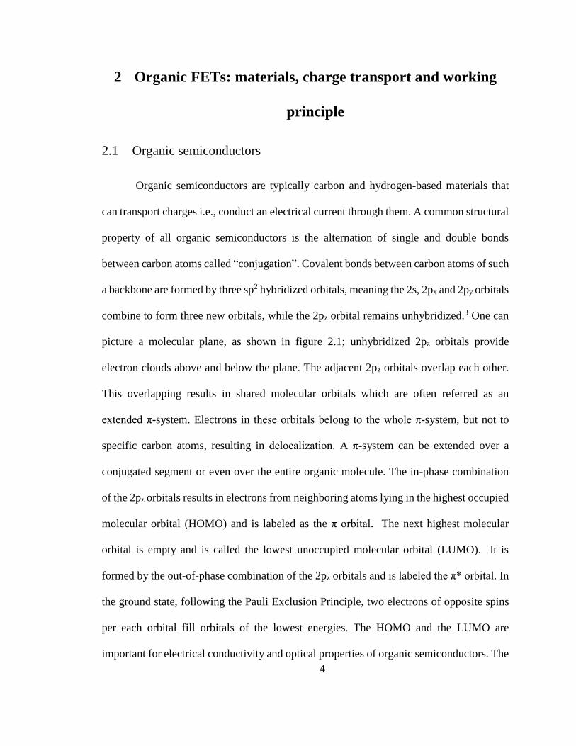
picture a molecular plane, as shown in figure 2.1; unhybridized 2pz orbitals provide
electron clouds above and below the plane. The adjacent 2pz orbitals overlap each other.
This overlapping results in shared molecular orbitals which are often referred as an
extended π-system. Electrons in these orbitals belong to the whole π-system, but not to
specific carbon atoms, resulting in delocalization. A π-system can be extended over a
conjugated segment or even over the entire organic molecule. The in-phase combination
of the 2pz orbitals results in electrons from neighboring atoms lying in the highest occupied
molecular orbital (HOMO) and is labeled as the π orbital. The next highest molecular
orbital is empty and is called the lowest unoccupied molecular orbital (LUMO). It is
formed by the out-of-phase combination of the 2pz orbitals and is labeled the π* orbital. In
the ground state, following the Pauli Exclusion Principle, two electrons of opposite spins
per each orbital fill orbitals of the lowest energies. The HOMO and the LUMO are
important for electrical conductivity and optical properties of organic semiconductors. The
5
energy difference between the HOMO and LUMO level is crucial from a device
perspective, and typically has values between 1.5 and 3.5 eV for organic semiconductors.
The typical HOMO-LUMO gap of semiconductors we used in this research is about 2 eV.
Figure 2.1 (a) Conjugated backbone and 2Pz orbitals pointing out of the molecular plane (b) highest occupied
molecular orbitals and lowest unoccupied molecular orbital. The red arrows indicate the spin of electrons.
In this work we use small molecule organic semiconductors: pentacene,
dinaphtho[2,3-b:2',3'- f]thieno[3,2-b]thiophene (DNTT), and 6,13-
bis(triisopropylsilylethynyl)pentacene (TIPS-pentacene). Pentacene is an aromatic
hydrocarbon comprised of five fused benzene rings and has been extensively studied
because of its ability to provide comparatively high charge carrier mobility for an organic
semiconductor.4, 5 Pentacene forms polycrystalline films in a herringbone packing
structure. Thermally evaporated pentacene films form single crystal islands on the surface
of the dielectric, generally dendritic in shape.6 Like most of the small molecule
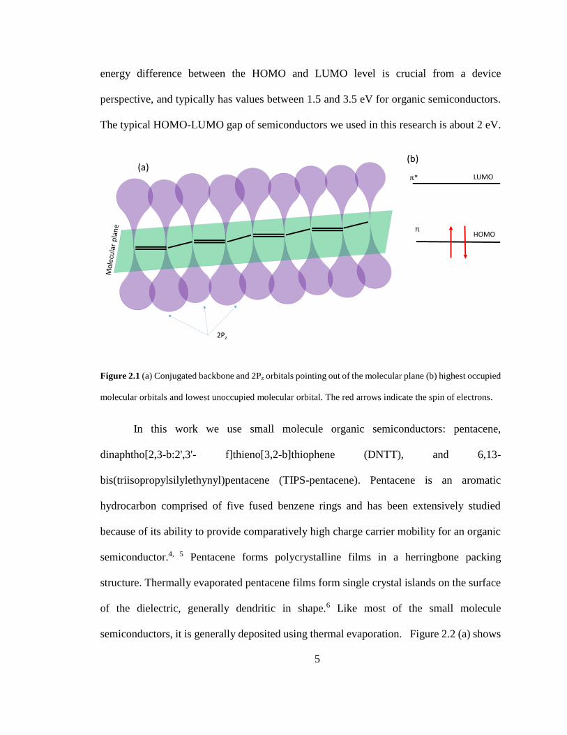
semiconductors, it is generally deposited using thermal evaporation. Figure 2.2 (a) shows
2Pz
LUMO
HOMO
π*
π
(a)(b)
6
the molecular structure of pentacene and figure 2.2 (b) shows an AFM images along with
a molecular model superimposed. This image was adapted from reference. 7
Figure 2.2 (a) Molecular structure of pentacene (b) 3 × 3 nm2 STM images of pentacene molecules adsorbed
on a Ni(111) substrate at RT (1.49 nA and 1.8 mV. A molecular model was also superimposed (adapted from
reference [7])
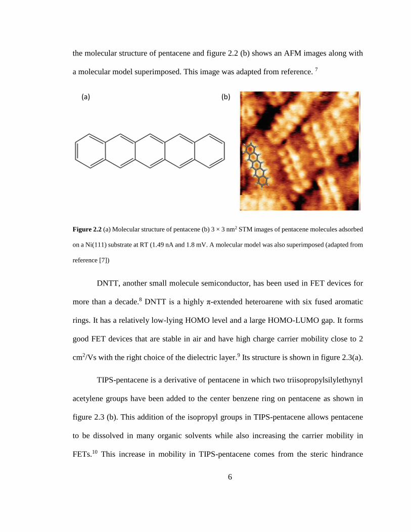
DNTT, another small molecule semiconductor, has been used in FET devices for
more than a decade.8 DNTT is a highly π-extended heteroarene with six fused aromatic
rings. It has a relatively low-lying HOMO level and a large HOMO-LUMO gap. It forms
good FET devices that are stable in air and have high charge carrier mobility close to 2
cm2/Vs with the right choice of the dielectric layer.9 Its structure is shown in figure 2.3(a).
TIPS-pentacene is a derivative of pentacene in which two triisopropylsilylethynyl
acetylene groups have been added to the center benzene ring on pentacene as shown in
figure 2.3 (b). This addition of the isopropyl groups in TIPS-pentacene allows pentacene
to be dissolved in many organic solvents while also increasing the carrier mobility in
FETs.10 This increase in mobility in TIPS-pentacene comes from the steric hindrance
(a) (b)
7
introduced by the long sidechains. The packing of TIPS-pentacene molecules is restricted
resulting in high π-π overlap. The increase in π-π overlap allows charges to be easily
transferred between TIPS-pentacene molecules. Among the solution processable small
molecule organic semiconductors, TIPS-pentacene has received a lot of attention in
FETs.10-12
Figure 2.3 Molecular structure of (a) dinaphtho[2,3-b:2',3'- f]thieno[3,2-b]thiophene (DNTT), and (b)6,13-
bis(triisopropylsilylethynyl)pentacene (TIPS-pentacene).
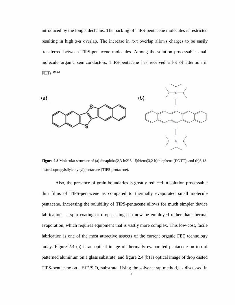
Also, the presence of grain boundaries is greatly reduced in solution processable
thin films of TIPS-pentacene as compared to thermally evaporated small molecule
pentacene. Increasing the solubility of TIPS-pentacene allows for much simpler device
fabrication, as spin coating or drop casting can now be employed rather than thermal
evaporation, which requires equipment that is vastly more complex. This low-cost, facile
fabrication is one of the most attractive aspects of the current organic FET technology
today. Figure 2.4 (a) is an optical image of thermally evaporated pentacene on top of
patterned aluminum on a glass substrate, and figure 2.4 (b) is optical image of drop casted
TIPS-pentacene on a Si++/SiO2 substrate. Using the solvent trap method, as discussed in
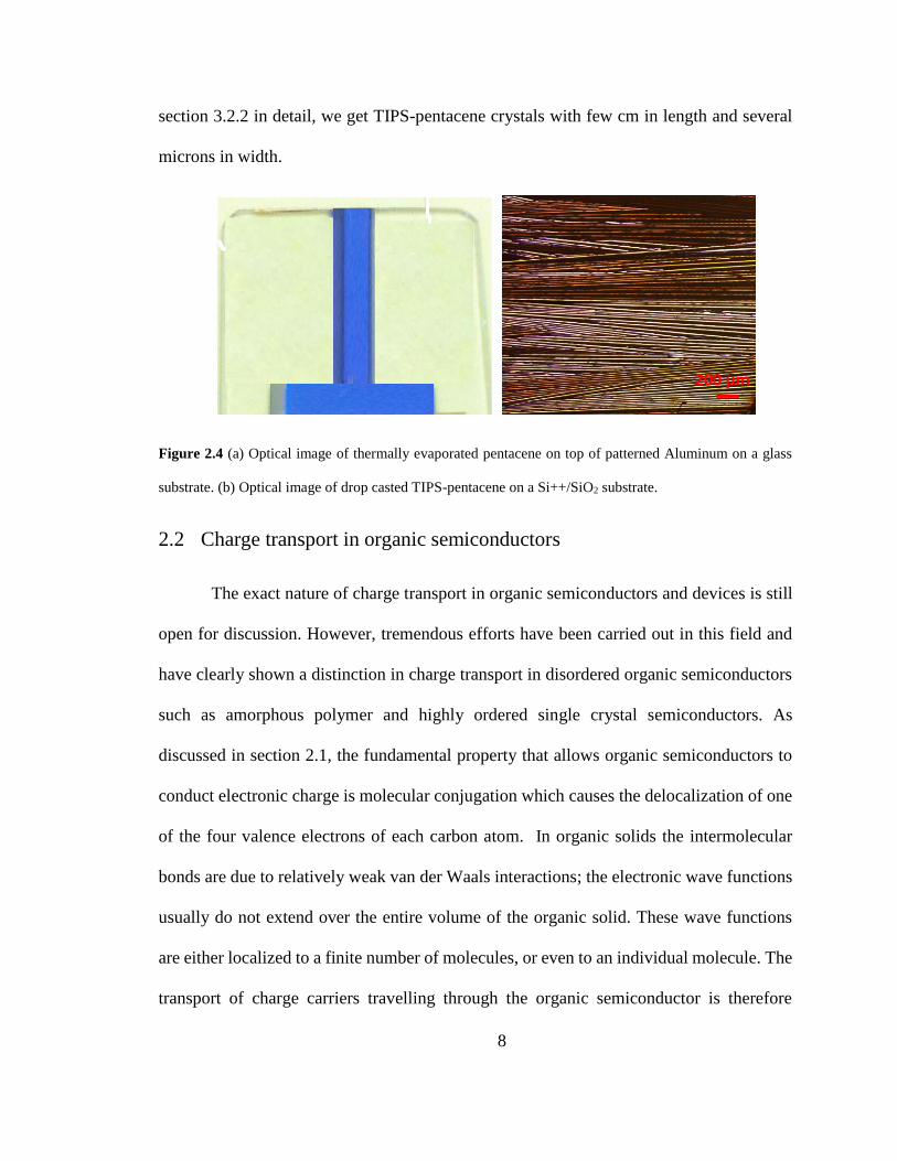
8
section 3.2.2 in detail, we get TIPS-pentacene crystals with few cm in length and several
microns in width.
Figure 2.4 (a) Optical image of thermally evaporated pentacene on top of patterned Aluminum on a glass
substrate. (b) Optical image of drop casted TIPS-pentacene on a Si++/SiO2 substrate.
2.2 Charge transport in organic semiconductors
The exact nature of charge transport in organic semiconductors and devices is still
open for discussion. However, tremendous efforts have been carried out in this field and
have clearly shown a distinction in charge transport in disordered organic semiconductors
such as amorphous polymer and highly ordered single crystal semiconductors. As
discussed in section 2.1, the fundamental property that allows organic semiconductors to
conduct electronic charge is molecular conjugation which causes the delocalization of one
of the four valence electrons of each carbon atom. In organic solids the intermolecular
bonds are due to relatively weak van der Waals interactions; the electronic wave functions
usually do not extend over the entire volume of the organic solid. These wave functions
are either localized to a finite number of molecules, or even to an individual molecule. The
transport of charge carriers travelling through the organic semiconductor is therefore
200 µm
9
determined by the ease with which electrons are transported from one molecule to the next
under the influence of an applied electric field. Since the carriers are not transported in
traditional electronic bands, carrier mobility in organic semiconductors is expected to be
thermally activated. Thermally activated charge transport, in general, is much smaller than
the charge transport in silicon based and other inorganic semiconductor crystals.13-15
The transport of charges in organic molecules rely on a thermally assisted hopping
mechanism via a Gaussian distribution of electronic states (discussed in detail in chapter
5). Charge transport in organic semiconductors, therefore, depends on the packing of
semiconductor polymer chains or small molecules and the density of structural defects.
Band to band transfer is much faster due to the available energy sites all having the same
energy, while hopping transport requires charge carriers to change levels to move across
the material. The fastest hopping transport occurs when there is a very tight distribution
of available energy states and defects in the semiconductor are minimized. Because no
single transport model can account for this wide range of observed carrier mobilities,
several models have been proposed to describe charge transport in organic materials:
variable range hopping,16 delocalized charge transport,17 multiple trapping and release,18
and other hybrid models.19 The model of variable-range hopping (VRH) assumes that
charge carriers hop between localized electronic states by quantum-mechanical tunneling
through energy barriers and that the probability of a hopping event is determined by the
hopping distance along with the energy distribution of the localized states. Specifically,
carriers can hop over short distances or over long distances depending upon large activation
energies or small activation energies, respectively. The variable-range hopping model is
usually discussed in the context of amorphous semiconductor films with room-temperature
10
mobilities below about 10-2 cm2 /Vs. Many small-molecule organic semiconductors have,
however, a strong tendency to form polycrystalline films. Because of the regular molecular
arrangement, the delocalized orbitals of neighboring molecules partially overlap, thereby
facilitating efficient intermolecular charge-carrier transfer and carrier mobilities that are
much larger than in amorphous films, usually well above 10-2 cm2 /Vs. Such large
mobilities are not easily explained with the variable-range hopping model.
In contrast to the variable-range hopping model, the multiple trapping and release
(MTR) model adapted for organic transistors by Gilles Horowitz20 and co-workers assumes
that most of the charge carriers in the channel are trapped in localized states (that are
associated with structural or chemical defects), and that carriers cannot move directly from
one state to another. Instead, carriers are temporarily promoted to an extended-state band
in which charge transport occurs.
Furthermore, temperature-dependent time-of-flight mobility measurements on
highly purified pentacene crystals have shown clear evidence for charge transport in
extended states with a hole mobility that is within an order of magnitude of the hole
mobility in single-crystalline silicon and is limited by phonon scattering, rather than
thermal activation.21
Charge transport in organic semiconductors also depend upon the device they are
used for. Our research is focused on charge transport in organic thin film transistors. The
dimensions of organic transistors usually far exceed the dimensions of an individual
molecule. Therefore, organic transistors typically utilize a thin film in which many
11
conjugated molecules are arranged in an ordered fashion. Charge transport in organic thin
film transistors and diodes is discussed in more detail in chapter 5.
2.3 Dielectrics used in organic FETs
Dielectrics can transfer electric effects without conducting electricity and can be
polar or non-polar. Polar dielectrics are those in which the molecules have a permanent
dipole moment as their centers of the positive and negative charges do not coincide. The
molecules are asymmetric in shape. In the case of non-polar dielectrics, the centers of both
positive as well as negative charges coincide. The dipole moment of each molecule in a
non-polar system is thus zero. Dielectrics can also be categorized as ferroelectric or non-
ferroelectric. The name “ferroelectricity” comes from an analogy to ferromagnetism (the
presence of a permanent magnetic moment), which was discovered prior to ferroelectricity.
Ferroelectricity is a phenomenon occurring in certain materials that arises from separation
of charges. 22 It refers to a spontaneous electric polarization that can be manipulated upon
the application of an electric field. Dielectrics are capacitors that accumulate charges upon
application of an electric field. In non-polar dielectrics, charge accumulation varies linearly
with applied field and saturates at some field. Upon reversing the field, the curve follows
the same path back. Figure 2.5 (a) shows variation of charge accumulation with voltage in
non-polar dielectric. In polar dielectrics, polarization curve does not follow back the curve
once it achieves saturation (Ps). There will be some remnant polarization (Pr) even after the
removal of an external field. The remnant polarization signifies that a high number of
dipoles remain aligned and can be flipped only when a minimum electric field required to
reorient the dipoles, defined as the coercive field, of the opposite polarity is applied. Figure
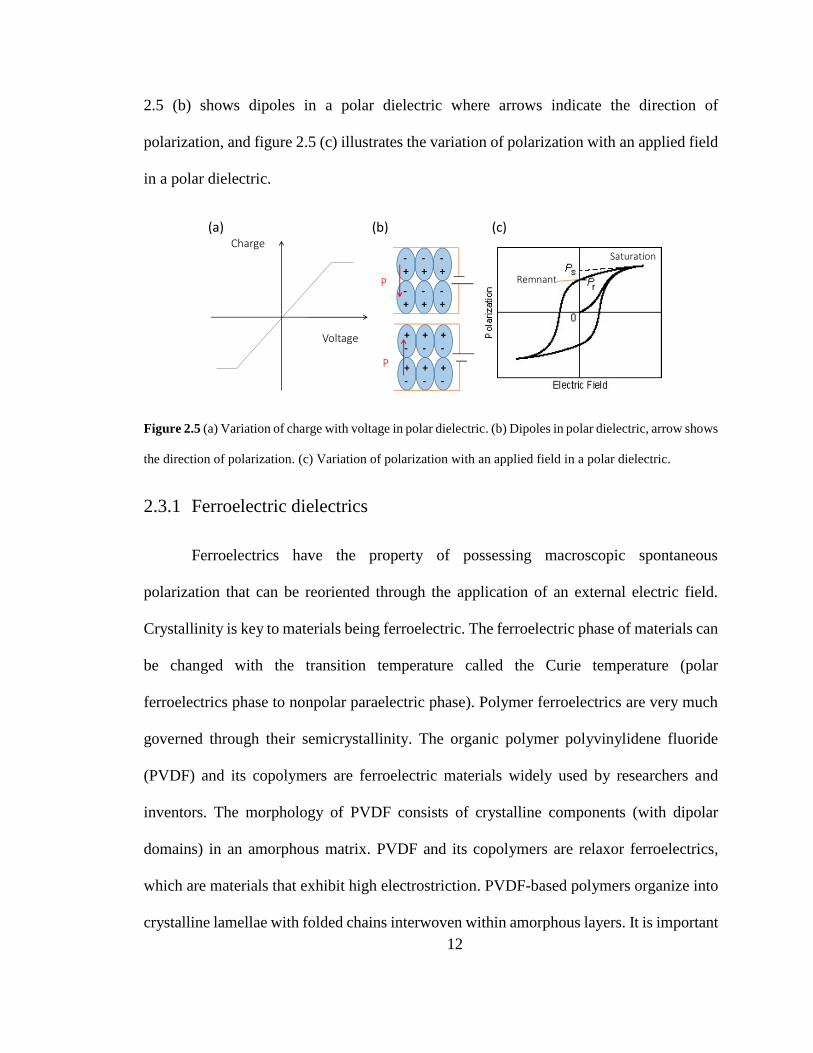
12
2.5 (b) shows dipoles in a polar dielectric where arrows indicate the direction of
polarization, and figure 2.5 (c) illustrates the variation of polarization with an applied field
in a polar dielectric.
Figure 2.5 (a) Variation of charge with voltage in polar dielectric. (b) Dipoles in polar dielectric, arrow shows
the direction of polarization. (c) Variation of polarization with an applied field in a polar dielectric.
2.3.1 Ferroelectric dielectrics
Ferroelectrics have the property of possessing macroscopic spontaneous
polarization that can be reoriented through the application of an external electric field.
Crystallinity is key to materials being ferroelectric. The ferroelectric phase of materials can
be changed with the transition temperature called the Curie temperature (polar
ferroelectrics phase to nonpolar paraelectric phase). Polymer ferroelectrics are very much
governed through their semicrystallinity. The organic polymer polyvinylidene fluoride
(PVDF) and its copolymers are ferroelectric materials widely used by researchers and
inventors. The morphology of PVDF consists of crystalline components (with dipolar
domains) in an amorphous matrix. PVDF and its copolymers are relaxor ferroelectrics,
which are materials that exhibit high electrostriction. PVDF-based polymers organize into
crystalline lamellae with folded chains interwoven within amorphous layers. It is important
Saturation
Remnant
+-
+-
+-
+-
+-
+-
-+
-+
-+
-+
-+
-+
P
P
Charge
Voltage
(a) (b) (c)
13
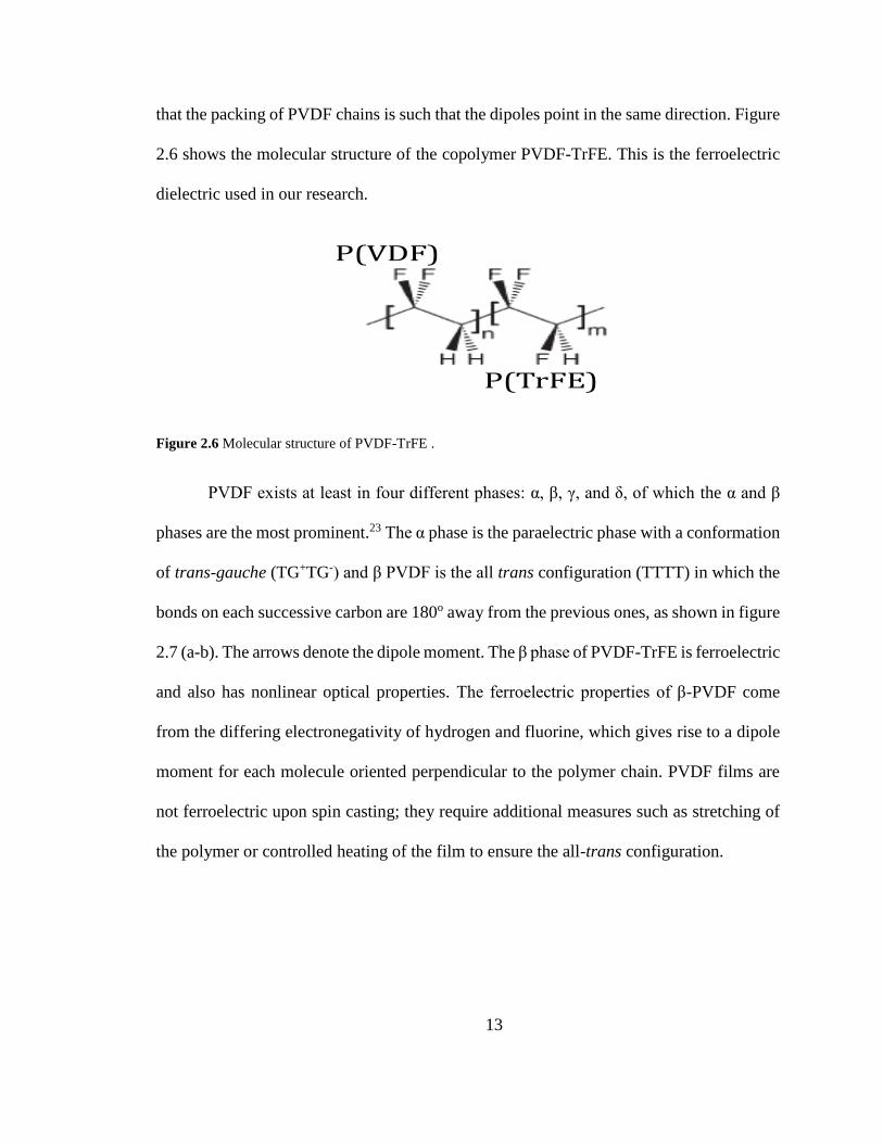
that the packing of PVDF chains is such that the dipoles point in the same direction. Figure
2.6 shows the molecular structure of the copolymer PVDF-TrFE. This is the ferroelectric
dielectric used in our research.
Figure 2.6 Molecular structure of PVDF-TrFE .
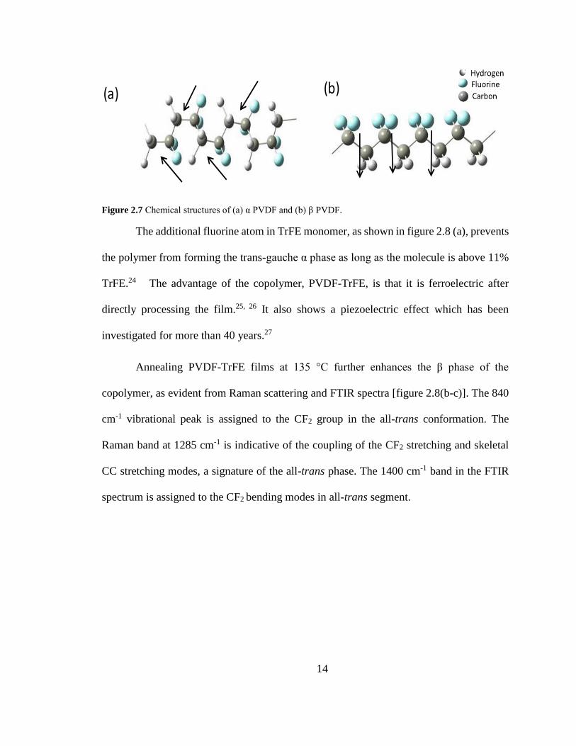
PVDF exists at least in four different phases: α, β, γ, and δ, of which the α and β
phases are the most prominent.23 The α phase is the paraelectric phase with a conformation
of trans-gauche (TG+TG-) and β PVDF is the all trans configuration (TTTT) in which the
bonds on each successive carbon are 180o away from the previous ones, as shown in figure
2.7 (a-b). The arrows denote the dipole moment. The β phase of PVDF-TrFE is ferroelectric
and also has nonlinear optical properties. The ferroelectric properties of β-PVDF come
from the differing electronegativity of hydrogen and fluorine, which gives rise to a dipole
moment for each molecule oriented perpendicular to the polymer chain. PVDF films are
not ferroelectric upon spin casting; they require additional measures such as stretching of
the polymer or controlled heating of the film to ensure the all-trans configuration.
P(VDF)
P(TrFE)
14
Figure 2.7 Chemical structures of (a) α PVDF and (b) β PVDF.
The additional fluorine atom in TrFE monomer, as shown in figure 2.8 (a), prevents
the polymer from forming the trans-gauche α phase as long as the molecule is above 11%
TrFE.24 The advantage of the copolymer, PVDF-TrFE, is that it is ferroelectric after
directly processing the film.25, 26 It also shows a piezoelectric effect which has been
investigated for more than 40 years.27
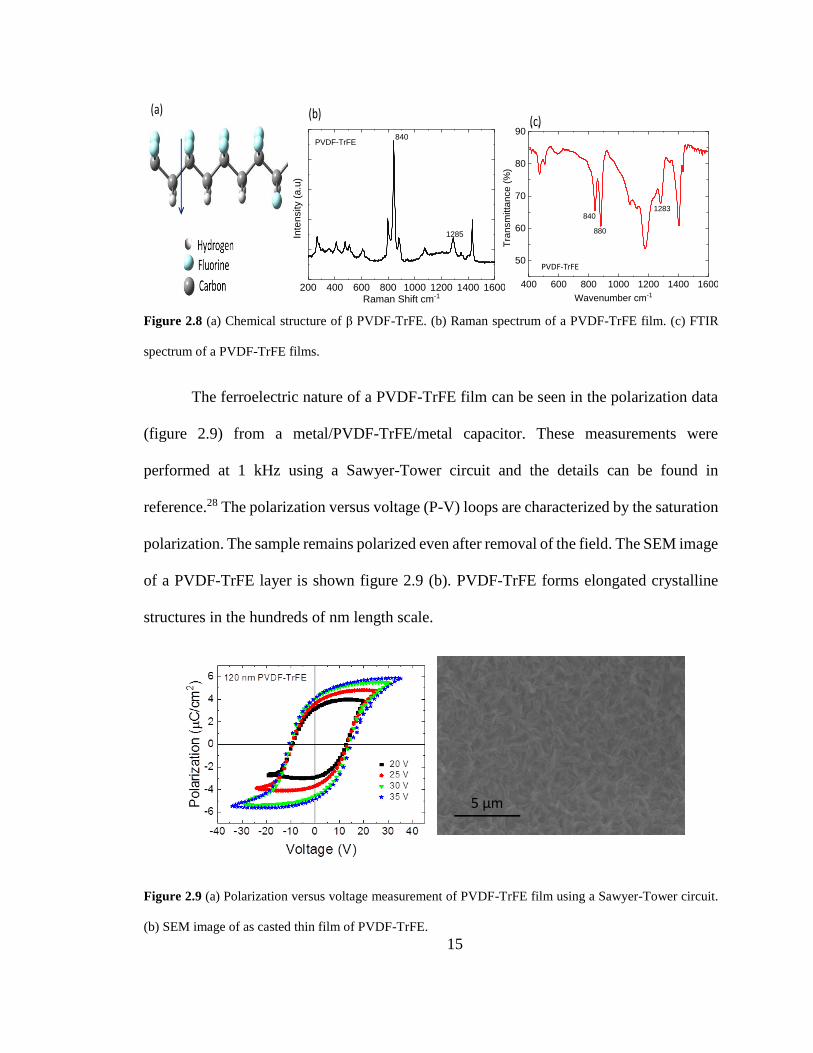
Annealing PVDF-TrFE films at 135 °C further enhances the β phase of the
copolymer, as evident from Raman scattering and FTIR spectra [figure 2.8(b-c)]. The 840
cm-1 vibrational peak is assigned to the CF2 group in the all-trans conformation. The
Raman band at 1285 cm-1 is indicative of the coupling of the CF2 stretching and skeletal
CC stretching modes, a signature of the all-trans phase. The 1400 cm-1 band in the FTIR
spectrum is assigned to the CF2 bending modes in all-trans segment.
200 400 600 800 1000 1200 1400 1600
1285Inte
nsity (
a.u
)
Raman Shift cm-1
PVDF-TrFE840
400 600 800 1000 1200 1400 1600
50
60
70
80
90
880
Tra
nsm
itta
nce (
%)
Wavenumber cm-1
8401283
PVDF-TrFE
(a) (b) (c)
(d) (e)
200 400 600 800 1000 1200 1400 1600
1285Inte
nsity (
a.u
)
Raman Shift cm-1
PVDF-TrFE840
400 600 800 1000 1200 1400 1600
50
60
70
80
90
880
Tra
nsm
itta
nce (
%)
Wavenumber cm-1
8401283
PVDF-TrFE
(a) (b) (c)
(d) (e)
15
Figure 2.8 (a) Chemical structure of β PVDF-TrFE. (b) Raman spectrum of a PVDF-TrFE film. (c) FTIR
spectrum of a PVDF-TrFE films.
The ferroelectric nature of a PVDF-TrFE film can be seen in the polarization data
(figure 2.9) from a metal/PVDF-TrFE/metal capacitor. These measurements were
performed at 1 kHz using a Sawyer-Tower circuit and the details can be found in
reference.28 The polarization versus voltage (P-V) loops are characterized by the saturation
polarization. The sample remains polarized even after removal of the field. The SEM image
of a PVDF-TrFE layer is shown figure 2.9 (b). PVDF-TrFE forms elongated crystalline
structures in the hundreds of nm length scale.
Figure 2.9 (a) Polarization versus voltage measurement of PVDF-TrFE film using a Sawyer-Tower circuit.
(b) SEM image of as casted thin film of PVDF-TrFE.
-30 -20 -10 0 10 20 30-9
-6
-3
0
3
6
9
30V
25V
20V
10V
Po
lariza
tio
n (
C
/cm
2)
Applied Voltage (V)
200 400 600 800 1000 1200 1400 1600
1285Inte
nsity (
a.u
)Raman Shift cm-1
PVDF-TrFE840
400 600 800 1000 1200 1400 1600
50
60
70
80
90
880
Tra
nsm
itta
nce (
%)
Wavenumber cm-1
8401283
PVDF-TrFE PVDF-TrFE
(a) (b) (c)
(d) (e) (f)
200 400 600 800 1000 1200 1400 1600
1285Inte
nsity (
a.u
)
Raman Shift cm-1
PVDF-TrFE840
400 600 800 1000 1200 1400 1600
50
60
70
80
90
880
Tra
nsm
itta
nce (
%)
Wavenumber cm-1
8401283
PVDF-TrFE
(a) (b) (c)
(d) (e)
(b)(c)
200 400 600 800 1000 1200 1400 1600
1285Inten
sity (a
.u)
Raman Shift cm-1
PVDF-TrFE840
400 600 800 1000 1200 1400 1600
50
60
70
80
90
880
T
ra
nsm
itta
nce (%
)
Wavenumber cm-1
8401283
PVDF-TrFE
(a) (b) (c)
(d) (e)
(a)
5 μm
16
2.3.1.1 Second harmonic generation
The β phase of PVDF and its copolymers lacks inversion symmetry and thus results
in second harmonic generation (SHG). SHG constitutes the process of doubling the
frequency of the incident light. The SHG interaction of the dominant electric-dipoles
involves three photons; two “input” photons of frequency ω, and one “output” photon of
frequency 2ω, and occurs in materials that do not possess inversion symmetry. Using a
classical nonlinear electron spring model, we know that light-matter interaction results in
an electronic polarization (P), which is not just linearly proportional to the electric field
(E), but also has contributions from higher powers of E:
�� (𝜔) = 𝑃0 + 𝜀0𝜒𝑒�� (𝜔) + 𝜒(2)�� (𝜔) 2 + 𝜒(3)�� (𝜔) 3 +⋯, (2.1)
where the second order susceptibility, 𝜒(2), a third-rank tensor (𝜒𝑖𝑗𝑘), is responsible for the
SHG phenomenon of doubling the frequency (ω). Schematics for our SHG experimental
setup in the transmission geometry is shown in figure 2.10.
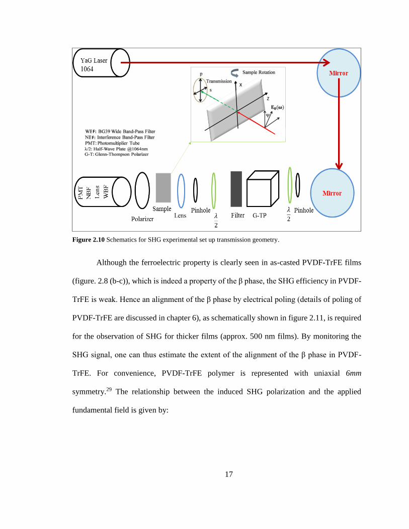
17
Figure 2.10 Schematics for SHG experimental set up transmission geometry.
Although the ferroelectric property is clearly seen in as-casted PVDF-TrFE films
(figure. 2.8 (b-c)), which is indeed a property of the β phase, the SHG efficiency in PVDF-
TrFE is weak. Hence an alignment of the β phase by electrical poling (details of poling of
PVDF-TrFE are discussed in chapter 6), as schematically shown in figure 2.11, is required
for the observation of SHG for thicker films (approx. 500 nm films). By monitoring the
SHG signal, one can thus estimate the extent of the alignment of the β phase in PVDF-
TrFE. For convenience, PVDF-TrFE polymer is represented with uniaxial 6mm
symmetry.29 The relationship between the induced SHG polarization and the applied
fundamental field is given by:
F:
F:
18
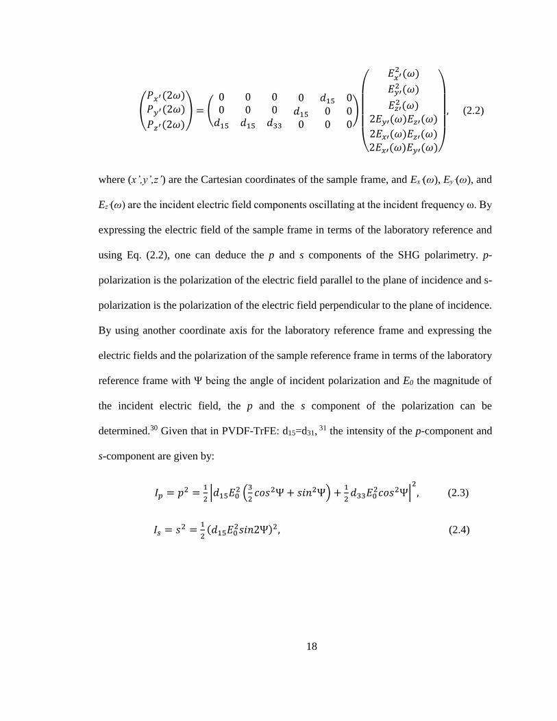
(
𝑃𝑥′(2𝜔)
𝑃𝑦′(2𝜔)
𝑃𝑧′(2𝜔)
) = (0 0 00 0 0𝑑15 𝑑15 𝑑33
0 𝑑15 0𝑑15 0 00 0 0
)
(
𝐸𝑥′2 (𝜔)
𝐸𝑦′2 (𝜔)
𝐸𝑧′2 (𝜔)
2𝐸𝑦′(𝜔)𝐸𝑧′(𝜔)
2𝐸𝑥′(𝜔)𝐸𝑧′(𝜔)2𝐸𝑥′(𝜔)𝐸𝑦′(𝜔))
, (2.2)
where (x’,y’,z’) are the Cartesian coordinates of the sample frame, and Ex’(ω), Ey’(ω), and
Ez’(ω) are the incident electric field components oscillating at the incident frequency ω. By
expressing the electric field of the sample frame in terms of the laboratory reference and
using Eq. (2.2), one can deduce the p and s components of the SHG polarimetry. p-
polarization is the polarization of the electric field parallel to the plane of incidence and s-
polarization is the polarization of the electric field perpendicular to the plane of incidence.
By using another coordinate axis for the laboratory reference frame and expressing the
electric fields and the polarization of the sample reference frame in terms of the laboratory
reference frame with Ψ being the angle of incident polarization and E0 the magnitude of
the incident electric field, the p and the s component of the polarization can be
determined.30 Given that in PVDF-TrFE: d15=d31, 31 the intensity of the p-component and
s-component are given by:
𝐼𝑝 = 𝑝2 =
1
2|𝑑15𝐸0
2 (3
2𝑐𝑜𝑠2Ψ+ 𝑠𝑖𝑛2Ψ) +
1
2𝑑33𝐸0
2𝑐𝑜𝑠2Ψ|2
, (2.3)
𝐼𝑠 = 𝑠2 =
1
2(𝑑15𝐸0
2𝑠𝑖𝑛2Ψ)2, (2.4)
19
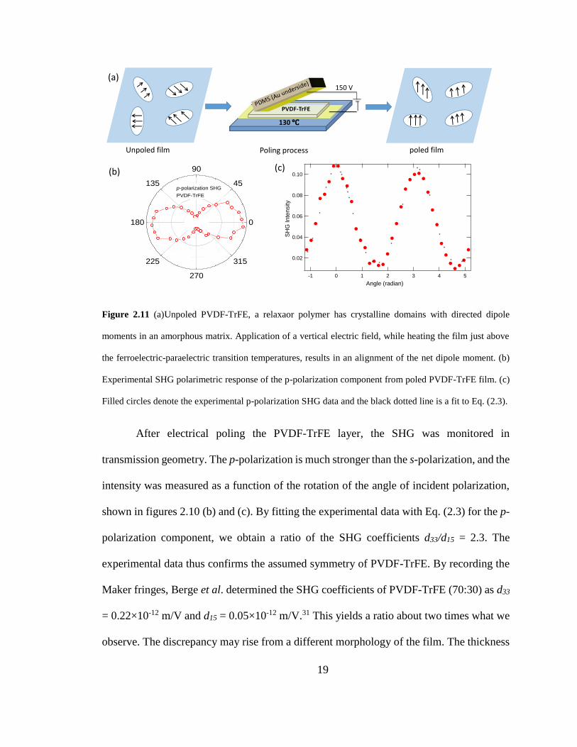
Figure 2.11 (a)Unpoled PVDF-TrFE, a relaxaor polymer has crystalline domains with directed dipole
moments in an amorphous matrix. Application of a vertical electric field, while heating the film just above
the ferroelectric-paraelectric transition temperatures, results in an alignment of the net dipole moment. (b)
Experimental SHG polarimetric response of the p-polarization component from poled PVDF-TrFE film. (c)
Filled circles denote the experimental p-polarization SHG data and the black dotted line is a fit to Eq. (2.3).
After electrical poling the PVDF-TrFE layer, the SHG was monitored in
transmission geometry. The p-polarization is much stronger than the s-polarization, and the
intensity was measured as a function of the rotation of the angle of incident polarization,
shown in figures 2.10 (b) and (c). By fitting the experimental data with Eq. (2.3) for the p-
polarization component, we obtain a ratio of the SHG coefficients d33/d15 = 2.3. The
experimental data thus confirms the assumed symmetry of PVDF-TrFE. By recording the
Maker fringes, Berge et al. determined the SHG coefficients of PVDF-TrFE (70:30) as d33
= 0.22×10⁻¹² m/V and d15 = 0.05×10⁻¹² m/V.31 This yields a ratio about two times what we
observe. The discrepancy may rise from a different morphology of the film. The thickness
150 V
130 °C
Unpoled film Poling process poled film
0
45
90
135
180
225
270
315
p-polarization SHG
PVDF-TrFE
0.10
0.08
0.06
0.04
0.02
SH
G I
nte
nsity
543210-1
Angle (radian)
(a)
(b) (c)
20
of the film in our experiment is much lower compared to Ref. 31, which may yield
differences in the ferroelectric domains. The SHG experiments therefore confirm the
structure of PVDF-TrFE as well as indicate the extent of poling. The poled films are further
utilized in FETs for monitoring transport, as discussed in chapter 5.
2.3.2 Non-polar (non-ferroelectric) dielectrics
Devices discussed in this work also make use of other organic and organic-
inorganic stacked dielectrics. The other two organic insulators used in this research are
poly-4-vinylphenol (PVP) and CYTOP. PVP is one of the most widely used insulators for
organic FET devices because of its ability to provide high carrier mobility and stable
devices.32 The monomer is an ethylene with one of the carbons containing a 4-phenol
group. The “4” in 4-phenol refers to the position of the OH group on the phenyl group. The
“1” position is the carbon connected to the ethylene group and the carbons are numbered
around the 6-carbon ring in order to give the lowest number to the other attached groups.
“4” is directly opposite the “1” position. The backbone of the polymer chain is formed by
these ethylene groups. Both printed and spin-casted PVP thin films have been used in this
work. The other dielectric used in this study is CYTOP. It is an amorphous fluoropolymer
with high optical transparency and excellent electrical and surface properties. It has good
solubility in certain fluorinated solvents due to its amorphous nature. The advantage of this
fluorinated solvent is it does not interact with the organic materials allowing the ability to
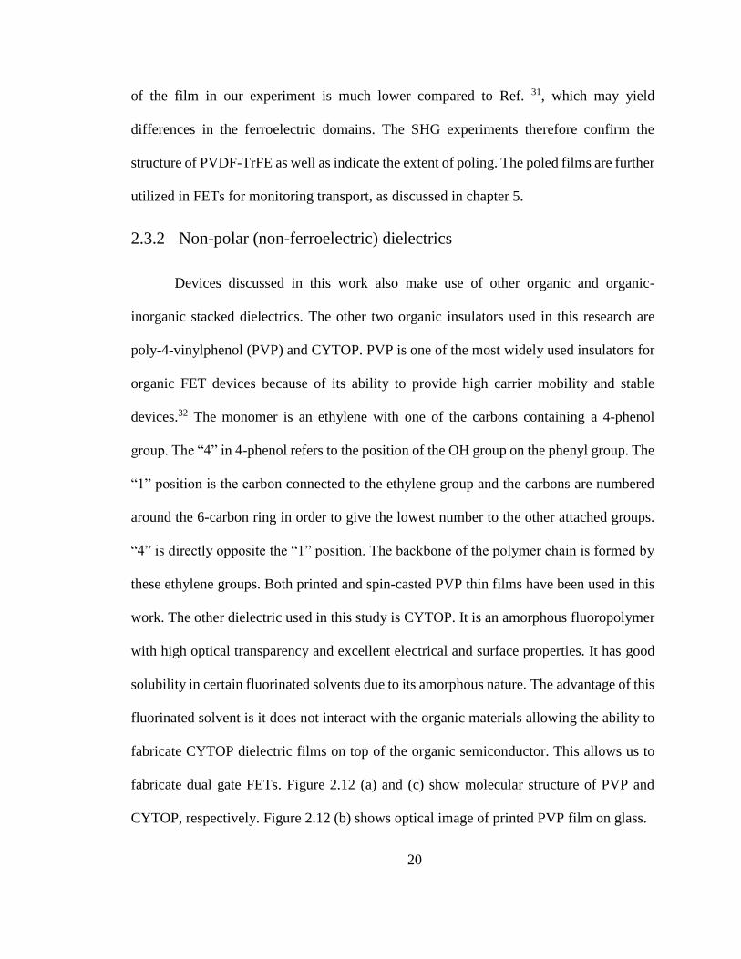
fabricate CYTOP dielectric films on top of the organic semiconductor. This allows us to
fabricate dual gate FETs. Figure 2.12 (a) and (c) show molecular structure of PVP and
CYTOP, respectively. Figure 2.12 (b) shows optical image of printed PVP film on glass.
21
Figure 2.12 (a) Molecular structure of PVP (b) Optical image of printed PVP (c) Molecular structure of
CYTOP.
Inorganic dielectrics used in this work are SiO2 and Al2O3. Al2O3 has higher
dielectric constants that that of SiO2, which is useful for FET device applications because
a high dielectric constant means an increased capacitance, which translates to a larger
magnitude of charge accumulated in the conduction channel at lower applied gate voltages.
It is important to have low operating voltages in order to reduce the power consumption of
transistors. It has been shown that the use of SiO2 as the insulating layer in pentacene FETs
leads to an increase in voltage required to form a conducting channel in the semiconductor
layer, a decrease in mobility, and an increase in operating voltage.33 In this work the use of
inorganic and non-ferroelectric dielectrics are mainly for a comparative study with the
polymer ferroelectric dielectric PVDF-TrFE. Table 2-I lists of dielectrics used along with
their corresponding dielectric constant.
CF2n
O
CF2CF2
CF2
CF2
CF2
(a) (c)(b)
22
Table 2-I Dielectric constant of dielectrics used in this research.
Dielectrics used Dielectric constant
SiO2 3.9
Al2O3 10
PVP 3.9
PMMA 3.5
CYTOP 2
PVDF-TrFE 8.3 (at 300 K)
2.4 Working principle of organic FETs
An FET is a three terminal electronic device where a field is applied to one terminal,
called the “gate”, resulting in the formation of a conductive channel between the other two
terminals known as the “source” and “drain”. FETs are comprised of multiple thin films.
Two basic components are the semiconductor and the dielectric layer. When a gate
potential is applied, it induces, via an electric field through a dielectric film, an
accumulation of charge carriers (electrons or holes) in the semiconducting layer. These
accumulated mobile charges then act as the conductive channel between the source and
drain electrodes. In an organic FET, the semiconducting layer is a thin film of an organic
semiconductor. The separation between source and drain is called “channel length” and the
width of the source or drain electrode is called “device width”.
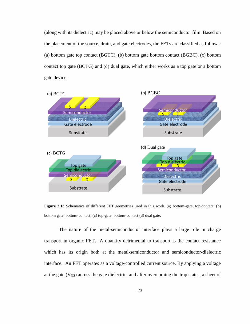
Figure 2.13 shows various types of geometries of organic FETs that are used in this
work. In an FET, the gate electrode is separated from the semiconducting layer by a
dielectric. The source and drain electrodes must be in direct contact with the semiconductor
as they will have to inject and extract charge carriers, respectively. The gate electrode
23
(along with its dielectric) may be placed above or below the semiconductor film. Based on
the placement of the source, drain, and gate electrodes, the FETs are classified as follows:
(a) bottom gate top contact (BGTC), (b) bottom gate bottom contact (BGBC), (c) bottom
contact top gate (BCTG) and (d) dual gate, which either works as a top gate or a bottom
gate device.
Figure 2.13 Schematics of different FET geometries used in this work. (a) bottom-gate, top-contact; (b)
bottom gate, bottom-contact; (c) top-gate, bottom-contact (d) dual gate.
The nature of the metal-semiconductor interface plays a large role in charge
transport in organic FETs. A quantity detrimental to transport is the contact resistance
which has its origin both at the metal-semiconductor and semiconductor-dielectric
interface. An FET operates as a voltage-controlled current source. By applying a voltage
at the gate (VGS) across the gate dielectric, and after overcoming the trap states, a sheet of
Substrate
Gate electrodeDielectric
SemiconductorS
Substrate
Gate electrodeDielectric
(b) BGBC
D
S DSemiconductor
Substrate
Gate electrodeDielectric
SemiconductorS D
(d) Dual gate
Top dielectricTop gate
Substrate
S D
(c) BCTG
SemiconductorTop dielectric
Top gate
(a) BGTC
24
mobile charge carriers is induced in the semiconductor that allows the drain current (IDS)
to flow through the semiconductor when another voltage between the drain-source (VDS)
is applied. The source contact is typically grounded.
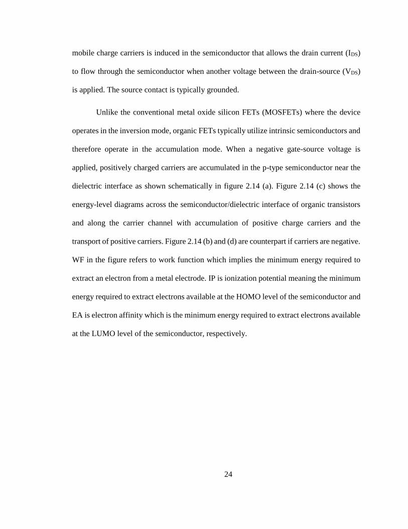
Unlike the conventional metal oxide silicon FETs (MOSFETs) where the device
operates in the inversion mode, organic FETs typically utilize intrinsic semiconductors and
therefore operate in the accumulation mode. When a negative gate-source voltage is
applied, positively charged carriers are accumulated in the p-type semiconductor near the
dielectric interface as shown schematically in figure 2.14 (a). Figure 2.14 (c) shows the
energy-level diagrams across the semiconductor/dielectric interface of organic transistors
and along the carrier channel with accumulation of positive charge carriers and the
transport of positive carriers. Figure 2.14 (b) and (d) are counterpart if carriers are negative.
WF in the figure refers to work function which implies the minimum energy required to
extract an electron from a metal electrode. IP is ionization potential meaning the minimum
energy required to extract electrons available at the HOMO level of the semiconductor and
EA is electron affinity which is the minimum energy required to extract electrons available
at the LUMO level of the semiconductor, respectively.
25
Figure 2.14 Energy-level diagrams across the semiconductor/dielectric interface of organic transistors and
along the carrier channel. Diagrams were drawn similar to Ref.14. (a) Accumulation of positive charge
carriers for negative gate-source voltages (p-channel transistor). (b) The accumulation of negative carriers
for positive gate-source voltages (n-channel transistor). (c) The transport of positive carriers from the source
through the semiconductor to the drain in the case of a p-channel transistor. (d) The transport of negative
carriers from the source through the semiconductor to the drain in the case of an n-channel transistor.
In p-channel transistors the transfer of negative charges into the semiconductor is
blocked due to the large energy difference between the Fermi level of the contact and the
LUMO of the semiconductor, and in n-channel transistors the transfer of positive charges
is blocked by the energy barrier between the contact and the HOMO of the
semiconductor.14, 15
(c) (d)
26
Though the physics of charge transport in organic FETs is different from that in
MOSFETs, the current–voltage characteristics can be described with the same formalism.
We use the long channel approximation where the horizontal electric field between the
drain and the source is very small compared to the vertical electric field induced by the
gate. When a potential is applied at the gate, a charge proportional to the capacitance of the
dielectric is induced at the dielectric-semiconductor interface. Traps within the
semiconducting layer are filled before the mobile charges begin to accumulate and form
the conducting channel. The gate voltage at which the conducting channel is formed is
referred to as the threshold voltage (VTh) similar to the gate voltage required to induce a
strong inversion layer in a MOSFET.34 The amount of charge along the channel varies
linearly as a function of the position when a drain-source bias is applied.
Provided that VGS>VTh, an increase in VDS but less than (VGS-VTh) results in charges
being accumulated and in an increase in IDS. The device is said to be in the linear regime.
If VDS is further increased such that VDS = VGS – VTh, the channel is “pinched off” and a
further increase in VDS will not result in an increase in IDS. In this case, the vertical electric
field in the channel close to the drain is insufficient to cause the accumulation of charge;
IDS is said to be saturated. Figure 2.15 shows the schematics for operating regimes of an
organic FET along with IDS versus VDS curves on the right.
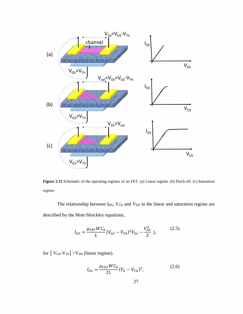
27
Figure 2.15 Schematic of the operating regimes of an FET. (a) Linear regime. (b) Pinch off. (c) Saturation
regime.
The relationship between IDS, VGS and VDS in the linear and saturation regime are
described by the Mott-Shockley equations,
𝐼𝐷𝑆 =
𝜇𝐹𝐸𝑇𝑊𝐶0𝐿
(𝑉𝐺𝑆 − 𝑉𝑇ℎ)2𝑉𝐷𝑠 −
𝑉𝐷𝑆2
2 ),
(2.5)
for │VGS-VTh│>VDS (linear regime).
𝐼𝐷𝑆 =
𝜇𝐹𝐸𝑇𝑊𝐶02𝐿
(𝑉𝐺 − 𝑉𝑇ℎ)2,
(2.6)
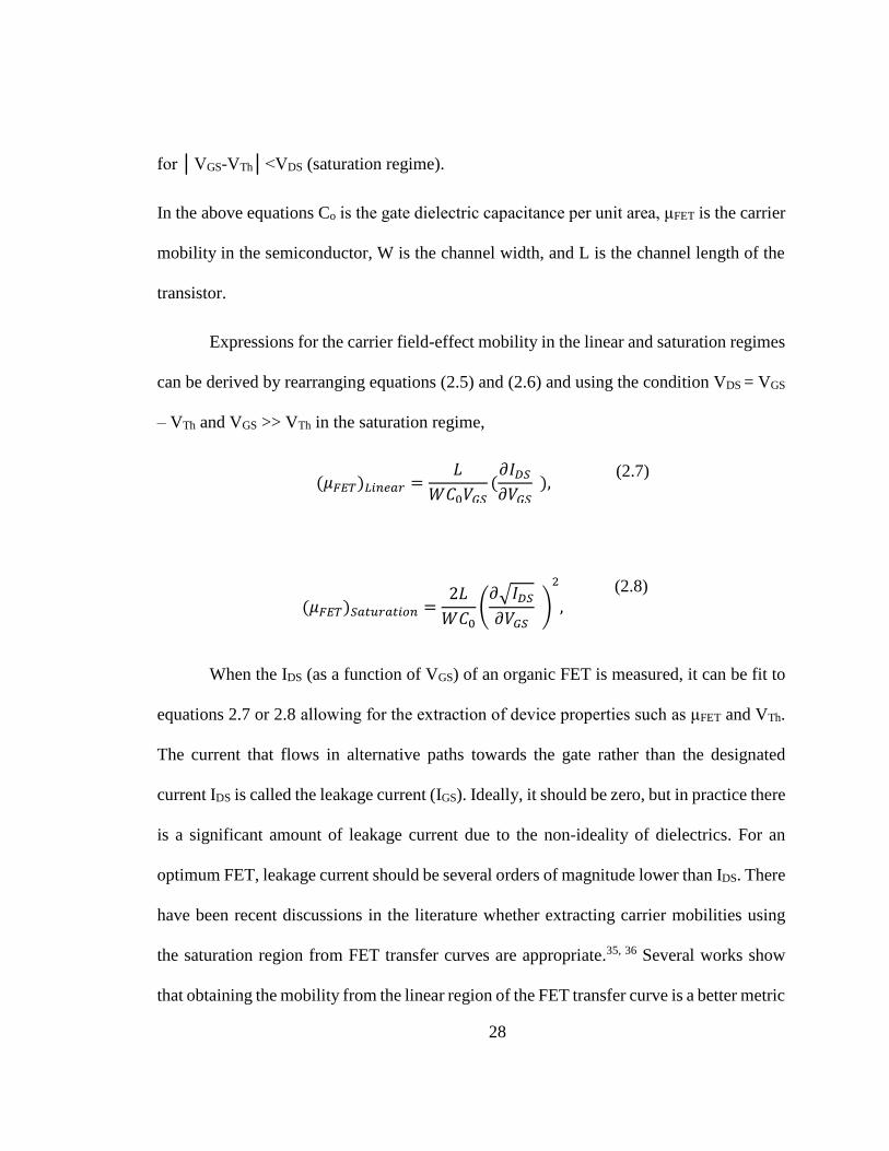
28
for │VGS-VTh│<VDS (saturation regime).
In the above equations Co is the gate dielectric capacitance per unit area, μFET is the carrier
mobility in the semiconductor, W is the channel width, and L is the channel length of the
transistor.
Expressions for the carrier field-effect mobility in the linear and saturation regimes
can be derived by rearranging equations (2.5) and (2.6) and using the condition VDS = VGS
– VTh and VGS >> VTh in the saturation regime,
(𝜇𝐹𝐸𝑇)𝐿𝑖𝑛𝑒𝑎𝑟 =
𝐿
𝑊𝐶0𝑉𝐺𝑆(𝜕𝐼𝐷𝑆𝜕𝑉𝐺𝑆
), (2.7)
(𝜇𝐹𝐸𝑇)𝑆𝑎𝑡𝑢𝑟𝑎𝑡𝑖𝑜𝑛 =2𝐿
𝑊𝐶0(𝜕√𝐼𝐷𝑆
𝜕𝑉𝐺𝑆 )
2
, (2.8)
When the IDS (as a function of VGS) of an organic FET is measured, it can be fit to
equations 2.7 or 2.8 allowing for the extraction of device properties such as μFET and VTh.
The current that flows in alternative paths towards the gate rather than the designated
current IDS is called the leakage current (IGS). Ideally, it should be zero, but in practice there
is a significant amount of leakage current due to the non-ideality of dielectrics. For an
optimum FET, leakage current should be several orders of magnitude lower than IDS. There
have been recent discussions in the literature whether extracting carrier mobilities using
the saturation region from FET transfer curves are appropriate.35, 36 Several works show
that obtaining the mobility from the linear region of the FET transfer curve is a better metric
29
for reliable mobilities. However, the linear region is also affected to a greater extent by
contact resistance compared to the saturation region, especially for small channel length
devices.37 A recent molecular-level FET device simulation shows that as long as the
energetic disorder of the semiconductor is lower than 2kBT (50 meV), the bulk mobility is
similar to saturation and linear mobility.38
Analysis of current-voltage characteristics of an FET gives the critical device
parameters. The behavior of IDS as a function of VDS at various VGS is the output
characteristics of an FET. Figure 2.16(a) shows a sample set of output characteristics of an
FET based on PVDF-TrFE and TIPS-pentacene. As described above, for a given VGS, the
IDS will increase linearly with VDS until it becomes saturated. As VGS is increased to a
higher magnitude, the saturation point will move to a higher value and the saturation
current will increase as well. Because the charge carrier density in the semiconductor is a
function of the gate-source voltage, the drain current can be modulated by adjusting the
gate-source voltage. This modulation of the drain current with the gate-source voltage is
quantitatively described by the fundamental field-effect transistor parameter of
transconductance, which is denoted by gm,
𝑔𝑚 = (
𝜕𝐼𝐷𝑆𝜕𝑉𝐺𝑆
), (2.9)
for constant VDS.
The behavior of IDS as a function of VGS at a fixed value of VDS, known as the
operating voltage, is called transfer characteristics of an FET. Figure 2.16 (b) shows typical
transfer characteristics of an organic FET based on PVDF-TrFE and TIPS-pentacene. Here
30
we can see the switching behavior clearly. IDS increases quadratically with VGS, quickly
taking the transistor from an off state (where drain current reaches a minimum) to an on
state. It is seen from equation (2.6) that the square root of IDS should be linear with VGS in
the saturation regime. The square root of IDS is also plotted when plotting transfer
characteristics, as shown in figure 2.16 (b). A linear fit to this region allows for the
calculation of FET mobility by using equation (2.8). VTh is then obtained from this linear
fit equation as the x-intercept. The on/off ratio can also be easily obtained from the transfer
curve. The on/off ratio is the ratio of the on current, defined to be IDS when VGS is equal to
the device operating voltage, to the off current. The switch-on voltage marks the gate-
source voltage at which the drain current reaches a minimum value. 34
Figure 2.16 Sample (a) output and (b) transfer characteristics of an organic FET. In (a) four output curves
corresponding to four gate voltages are shown. The saturation of IDS is clearly seen in each of the curves. In
(b) both the IDS and the square root of IDS are plotted. IDS is plotted on a logarithm scale to better show the
switching behavior of the FET. The linear behavior of the square root of IDS is also clearly seen.
The subthreshold region is described below VTh where IDS depends exponentially
on VGS in the transfer curve. For the transistor as shown in figure 2.16 the subthreshold
-4 -3 -2 -1 010-11
10-10
10-9
10-8
10-7IDS
Cu
rre
nt
(A)
VGS (V)
on/off=104
mob=0.2 cm2/Vs
SS=350 mV/Decade
IGS
SS=1/slope
VTh0
2
4
I DS
1/2
(x10
4A
1/2
)
-3 -2 -1 0
-0.32
-0.24
-0.16
-0.08
0.00
I DS (
A
)
VDS (V)
0 V
-1 V
-2 V
-3 VSaturation regime
Linear regime
(a) (b)
VDS= -4 V
31
region extends between the switch-on voltage at -0.7 V and the threshold voltage at -1.3
V. In the subthreshold region the drain current is due to carriers that have enough thermal
energy to overcome the gate-voltage-controlled energy barrier near the source contact and
mainly diffuse, rather than drift, through the semiconductor to the drain contact. 34, 39 The
inverse of the slope of the log(IDS) versus VGS curve in the subthreshold region is called
subthreshold swing (SS) and is calculated by,
𝑠𝑠 = (
𝜕𝑙𝑜𝑔10 (𝐼𝐷𝑆)
𝜕𝑉𝐺𝑆 )
−1
, (2.10)
The subthreshold swing (SS) is determined by the density of trap states at the
semiconductor/dielectric interface. Since the dielectric-semiconductor interface for organic
semiconductor has a low quality due to noncrystalline nature of semiconductor the SS value
is large in organic FETs compared to MOSFETs.
32
3 Experimental methods
3.1 Substrate preparation
The quality of the substrate surface is very critical to any FET performance where
the metallic electrodes, dielectric and semiconductor layers are deposited immediately on
top of another. A dielectric layer and the nature of the dielectric surface (which depends on
the quality of substrate surface) are crucial in determining the ordering of the
semiconductor film and controlling the density of charge carrier traps. Much care was
given in the surface treatments to improve the surface and interface of thin film deposition.
This section contains the substrate preparation recipe that was used for all organic FET
fabrication.
Substrates used in this work are glass and Si++/SiO2, typically of 1x1-inch size. The
glass substrates and Si++/SiO2 wafers were obtained from Fisher Scientific and Silicon
Quest International, respectively. All substrates were first cleaned via an organic cleaning
process to remove soluble organic impurities. Generally, 4 pieces of substrates were
prepared at one time as we can fit all of them inside the thermal evaporator for
semiconductor/electrode deposition. Any loose dust left by the diamond scribe on the
substrate surface was quickly washed away by rinsing with isopropyl alcohol. Substrates
were then immediately submerged in acetone and ultrasonicated for 20 minutes (Aquasonic
model 50HT by VWR scientific products). Exposure to ultrasonic (>20 kHz) waves knocks
off and dissolves organic contaminants by causing small bubbles in the acetone to burst.
After ultrasonication, the substrates were removed from the acetone bath and quickly rinsed
with copious amounts of acetone followed by isopropyl alcohol. All traces of the organic
33
solvents were then removed from the substrates by rinsing with deionized water. Glass
substrates were then baked in a closed oven (Model 20 GC Lab Oven) at 100 °C to remove
any water residue while Si++/SiO2 substrates were subjected to further surface treatments.
To remove ionic contaminants and heavier organic residues which could be
insoluble in acetone and isopropyl alcohol, Si++/SiO2 substrates were followed by piranha
cleaning. A mixture of 7:3 (by volume) sulfuric acid (H2SO4) to hydrogen peroxide (H2O2)
constitutes the piranha. This solution is a highly acidic and a strongly oxidizing agent used
to clean organic and ionic impurities off the substrates. Since this reaction is very
exothermic, the piranha solution is capable of heating itself to temperatures well above the
boiling point of water. While sulfuric acid and hydrogen peroxide are mixed together the
acid forces the dissociation of the peroxide via protonation. The resultant atomic oxygen
is a highly reactive species capable of aggressively oxidizing carbon-bearing residues.
Thus, the piranha aggressively eats away organic residues from the surface of the
substrates. Immediately after the organic cleaning and rinsing with water, the substrates
were submerged in a heated piranha solution for 5 minutes. To ensure the solution was
ready when needed, it was prepared during the organic cleaning step. The prepared solution
was then heated on a hot plate (CIMAREC Barnstead Thermolyne) at 125°C to maintain
the temperature of piranha through the treatment. After five minutes in the heated solution,
the substrates were removed using plastic forceps and were thoroughly washed with
deionized water. The substrates were then dried with compressed air. The substrate surface
is highly hydrophilic in nature, which is a direct result of the strongly protonating piranha
solution. It is evident in the way water sheeted across the substrate surface. The substrates
were placed in containers and moved to a glovebox for storage.
34
After 24 hours the substrate surface was treated with octadecyltrichlorosilane
(OTS) solution to produce a self-assembled monolayer (SAM). The substrates that emerge
from the cleaning procedure are in a hydrated state, and it is vital to wait long enough
(overnight) before beginning the OTS surface modification. Details of the OTS SAM
deposition can be found in previous works from our research group.40 The OTS solution
was prepared in a freshly cleaned and dried glassware. Glassware was cleaned using
Liquinox Critical Cleaning Detergent (Alconox Inc.) and dried in a closed oven (Model 20
GC Lab Oven) at 120oC. The glassware was then allowed to cool to room temperature
before use. OTS (>90%, Sigma Aldrich) was dissolved in HPLC grade toluene (>99.9%,
Sigma Aldrich) at a concentration of 0.25g/10 ml in a small petri dish. The solution was
allowed to age 3 minutes, and then each substrate was submerged in the solution for 10 to
30s. The substrate was then submerged in fresh HPLC grade toluene while the remaining
substrates were treated in the OTS solution. It should be noted that the insertion of each
substrate degrades the OTS solution to the point that it can be only be used for 3-4
substrates. Then all the substrates were subjected to ultrasonication in toluene for 30s.
Finally, the completed substrates were rinsed with isopropyl alcohol and dried with
compressed air. After completion of the OTS treatment, the SiO2 surface was clean without
any cloudy residue. A successful OTS monolayer formation was confirmed by placing a
drop of water on the surface and examining the contact angle the drop forms with the
surface. It has been shown that the contact angle should be about 80o. 40 A surface with a
contact angle less than this is indicative of incomplete OTS coverage. If the above
described protocol ever results in incompletely covered substrates during a particular
session, it may be modified by dipping the substrates for a longer time (up to one minute).
35
3.2 Thin film fabrication
3.2.1 Spin-coating
Spin-coating is a widely employed technique in the deposition of polymeric thin
films onto flexible and non-flexible substrates. This method is used to deposit photoresist
in high volume manufacturing companies. The procedure can be summarized as: (a) an
amount of a solution is dispensed on the substrate (which is held in place by vacuum chuck)
either before substrate rotation, known as static dispatch, or while the substrate is rotating,
known as dynamic dispatch; (b) the substrate is rotated at a pre-set speed which may vary
between a few hundred to a few thousand rotations per minute (rpm); (c) the solution
spreads outwards, resulting in the formation of a thin film. Typically, the substrates, along
with the newly formed films, will then be baked at an elevated temperature (often under
vacuum) to drive off any remaining solvent left in the film. Some polymeric films are
baked at a desired temperature and time to enhance the film qualities like phase and
crystallinity. The spin-coating process leaves ample opportunity for customization of
different materials, solvents, and substrates. A small change in any of the steps as described
above may have drastic implications on film thickness, coverage, and uniformity. The film
property depends upon (1) the concentration of the solution, (2) the boiling point of the
solvent, (3) spin speed, (4) humidity, and (5) the surface of the substrate. For some
polymeric materials, because of their solubility, there may be restrictions on usable
solvents and maximum obtainable concentration. For highly hydrophobic substrate
surfaces, there may be a limitation to the lowest usable spin-speed, as at low speeds the
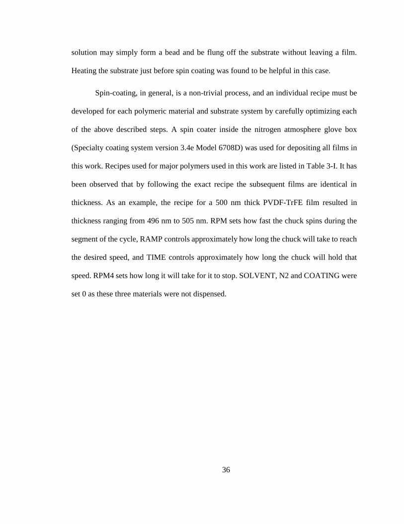
36
solution may simply form a bead and be flung off the substrate without leaving a film.
Heating the substrate just before spin coating was found to be helpful in this case.
Spin-coating, in general, is a non-trivial process, and an individual recipe must be
developed for each polymeric material and substrate system by carefully optimizing each
of the above described steps. A spin coater inside the nitrogen atmosphere glove box
(Specialty coating system version 3.4e Model 6708D) was used for depositing all films in
this work. Recipes used for major polymers used in this work are listed in Table 3-I. It has
been observed that by following the exact recipe the subsequent films are identical in
thickness. As an example, the recipe for a 500 nm thick PVDF-TrFE film resulted in
thickness ranging from 496 nm to 505 nm. RPM sets how fast the chuck spins during the
segment of the cycle, RAMP controls approximately how long the chuck will take to reach
the desired speed, and TIME controls approximately how long the chuck will hold that
speed. RPM4 sets how long it will take for it to stop. SOLVENT, N2 and COATING were
set 0 as these three materials were not dispensed.
37
Table 3-I Recipes used for spin coating of major polymers used in this work.
The dielectric layers of PVDF-TrFE dissolved in the solvent N,N-
dimethylformamide (DMF) were created with different concentrations: 1.8 wt. %, 2 wt. %
3.5 wt. %, 4 wt. %, 4.5 wt. %, and 16 wt. % of PVDF-TrFE. The solution was aged
overnight or heated at 80 °C (typically for higher wt. %) to completely dissolve the solute.
A few drops of the solution were dropped onto Al coated glass slides and spin coated at
1600 rpm for 60 s. The films were vacuum annealed at 135 °C for an hour and a half to
improve the crystallinity. The different concentrations resulted in the thickness of the
dielectric film to vary from 20 nm to 500 nm. The thicknesses of the films were measured
PVDF-TrFE CYTOP PVP/PMMA
RECIPE 0001 0002 0003
RPM1 0300 0300 0800
RAMP1 0002 0002 0001
TIME1 0010 0010 0005
RPM2 0600 0600 2500
RAMP2 0002 0002 0002
TIME2 0003 0003 0005
RPM3 1600 2000 5000
RAMP3 0005 0005 0005
TIME3 0060 0060 0040
RPM4 0001 0001 0001
SOLVENT 0000 0000 0000
N2 0000 0000 0000
COATING 0000 0000 0000
38
by a reflectometer (Mprobe, Inc.) and further confirmed by a profilometer and/or by
capacitance-voltage measurement.
Poly-4-vinyl phenol (PVP) with average molecular weight (MW) 25,000 g/mol,
propylene glycol monomethyl ether acetate (PGMEA) with MW 132.16 g/mol, and cross-
linking agent poly(melamine-coformaldehyde)methylated 84% solution in 1-butane
(PMMF), procured from Sigma Aldrich, were baked at 180 °C for 1 hour after spin coating
or printing. Poly(methyl methacrylate) (PMMA, Mw 996, 000), obtained from Sigma
Aldrich, was dissolved in dimethylsulfoxide (DMSO). Typical concentration was 6 wt. %
and the solution was put on a hot plate with a magnetic stirrer for 45 min. This film was
baked at 100 °C for 20 minutes. CYTOP (CTL-809M), bought from Asahi Glass Co. Ltd.,
Japan was diluted with CT-solv 180 and spin-coated on top of the semiconductor to design
top gate FETs. Since the polymer film suffers from cracking at high temperature, the films
were baked at 60 °C for a couple of hours.
3.2.2 Drop casting
The drop casting technique is typically employed in the deposition of polymeric
thin films onto flexible and non-flexible substrates. It is low cost, consumes little solution,
and is an easy method. The procedure could be as simple as dispensing solution onto a
substrate and letting the solution spread outwards and dry with a resultant thin film
formation. Several techniques and methods have been developed to modify the drop casting
method for enhancement of the resultant thin films. Here we discuss the drop casting recipe
that was used for solution processable organic semiconductors.
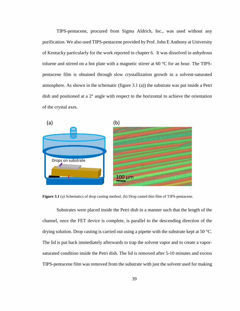
39
TIPS-pentacene, procured from Sigma Aldrich, Inc., was used without any
purification. We also used TIPS-pentacene provided by Prof. John E Anthony at University
of Kentucky particularly for the work reported in chapter 6. It was dissolved in anhydrous
toluene and stirred on a hot plate with a magnetic stirrer at 60 °C for an hour. The TIPS-
pentacene film is obtained through slow crystallization growth in a solvent-saturated
atmosphere. As shown in the schematic (figure 3.1 (a)) the substrate was put inside a Petri
dish and positioned at a 2° angle with respect to the horizontal to achieve the orientation
of the crystal axes.
Figure 3.1 (a) Schematics of drop casting method. (b) Drop casted thin film of TIPS-pentacene.
Substrates were placed inside the Petri dish in a manner such that the length of the
channel, once the FET device is complete, is parallel to the descending direction of the
drying solution. Drop casting is carried out using a pipette with the substrate kept at 50 °C.
The lid is put back immediately afterwards to trap the solvent vapor and to create a vapor-
saturated condition inside the Petri dish. The lid is removed after 5-10 minutes and excess
TIPS-pentacene film was removed from the substrate with just the solvent used for making
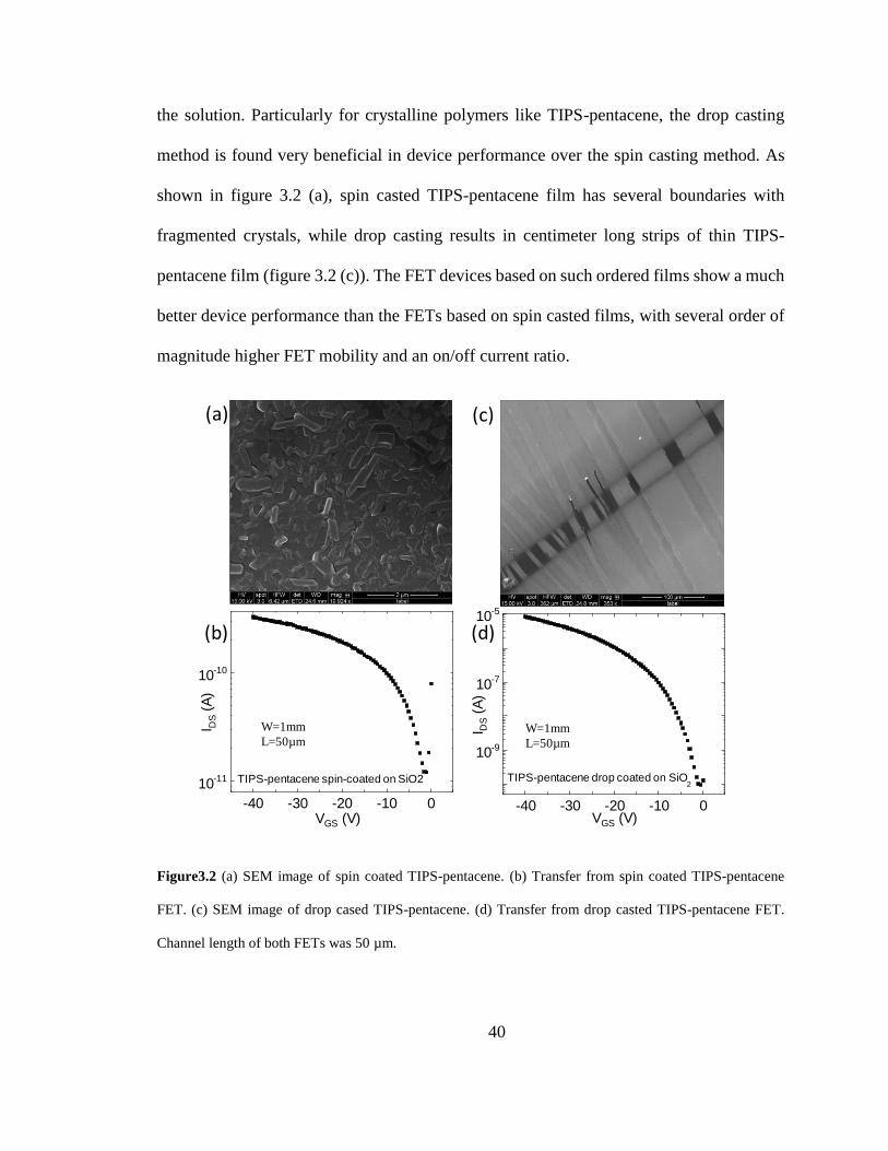
40
the solution. Particularly for crystalline polymers like TIPS-pentacene, the drop casting
method is found very beneficial in device performance over the spin casting method. As
shown in figure 3.2 (a), spin casted TIPS-pentacene film has several boundaries with
fragmented crystals, while drop casting results in centimeter long strips of thin TIPS-
pentacene film (figure 3.2 (c)). The FET devices based on such ordered films show a much
better device performance than the FETs based on spin casted films, with several order of
magnitude higher FET mobility and an on/off current ratio.
Figure3.2 (a) SEM image of spin coated TIPS-pentacene. (b) Transfer from spin coated TIPS-pentacene
FET. (c) SEM image of drop cased TIPS-pentacene. (d) Transfer from drop casted TIPS-pentacene FET.
Channel length of both FETs was 50 µm.
W=1mm
L=50µmW=1mm
L=50µm
-40 -30 -20 -10 0
10-11
10-10
I DS
(A)
VGS (V)
TIPS-pentacene spin-coated on SiO2
-40 -30 -20 -10 0
10-9
10-7
10-5
I DS
(A)
VGS (V)
2
(a)
(d)(b)
(c)
TIPS-pentacene drop coated on SiO
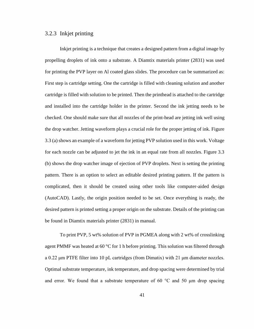
41
3.2.3 Inkjet printing
Inkjet printing is a technique that creates a designed pattern from a digital image by
propelling droplets of ink onto a substrate. A Diamtix materials printer (2831) was used
for printing the PVP layer on Al coated glass slides. The procedure can be summarized as:
First step is cartridge setting. One the cartridge is filled with cleaning solution and another
cartridge is filled with solution to be printed. Then the printhead is attached to the cartridge
and installed into the cartridge holder in the printer. Second the ink jetting needs to be
checked. One should make sure that all nozzles of the print-head are jetting ink well using
the drop watcher. Jetting waveform plays a crucial role for the proper jetting of ink. Figure
3.3 (a) shows an example of a waveform for jetting PVP solution used in this work. Voltage
for each nozzle can be adjusted to jet the ink in an equal rate from all nozzles. Figure 3.3
(b) shows the drop watcher image of ejection of PVP droplets. Next is setting the printing
pattern. There is an option to select an editable desired printing pattern. If the pattern is
complicated, then it should be created using other tools like computer-aided design
(AutoCAD). Lastly, the origin position needed to be set. Once everything is ready, the
desired pattern is printed setting a proper origin on the substrate. Details of the printing can
be found in Diamtix materials printer (2831) in manual.
To print PVP, 5 wt% solution of PVP in PGMEA along with 2 wt% of crosslinking
agent PMMF was heated at 60 °C for 1 h before printing. This solution was filtered through
a 0.22 μm PTFE filter into 10 pL cartridges (from Dimatix) with 21 μm diameter nozzles.
Optimal substrate temperature, ink temperature, and drop spacing were determined by trial
and error. We found that a substrate temperature of 60 °C and 50 μm drop spacing
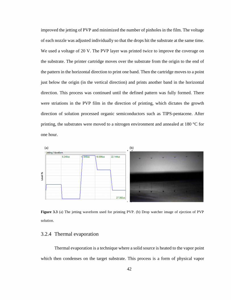
42
improved the jetting of PVP and minimized the number of pinholes in the film. The voltage
of each nozzle was adjusted individually so that the drops hit the substrate at the same time.
We used a voltage of 20 V. The PVP layer was printed twice to improve the coverage on
the substrate. The printer cartridge moves over the substrate from the origin to the end of
the pattern in the horizontal direction to print one band. Then the cartridge moves to a point
just below the origin (in the vertical direction) and prints another band in the horizontal
direction. This process was continued until the defined pattern was fully formed. There
were striations in the PVP film in the direction of printing, which dictates the growth
direction of solution processed organic semiconductors such as TIPS-pentacene. After
printing, the substrates were moved to a nitrogen environment and annealed at 180 °C for
one hour.
Figure 3.3 (a) The jetting waveform used for printing PVP. (b) Drop watcher image of ejection of PVP
solution.
3.2.4 Thermal evaporation
Thermal evaporation is a technique where a solid source is heated to the vapor point
which then condenses on the target substrate. This process is a form of physical vapor
(a) (b)
43
deposition and only useful for those materials that have a melting or sublimation temperate
much less than their decomposition temperature. The process may be summarized as
heating the solid by placing it in a boat made of a high melting point metal (or in a crucible)
until individual molecules or atoms have enough thermal energy to escape from the solid,
travel from the source to the substrate, and deposit on it, creating a film. These evaporated
particles should travel from the source to the substrate without colliding with ambient
molecules. So, the evaporation process must occur in vacuum.
In this work we used an MBraun thermal evaporation system where a typical
vacuum of ~ 10-5 mbar is obtained via Pfeifer vacuum turbomolecular pump backed by a
rotary vane pump (Edwards) referred to as the roughing pump. The roughing pump is used
to back the turbomolecular pump by maintaining a suitable exhaust pressure (~ 10-1 mbar).
Evacuation in the MBraun system begins by using the roughing pump to pump the chamber
down to ~200 mbar, at which point the turbomolecular pump starts and accelerates
appreciably after the roughing pump has pumped the chamber down to 10-1 mbar. The
evaporation chamber itself contains resistively heated sources, a substrate holder, and
quartz microbalance thickness monitors as shown in figure 3.4 (a). A tungsten boat is used
for the evaporation of aluminum and gold, a Molybdenum boat is used for the evaporation
of silver and calcium), and a quartz crucible is used for the evaporation of organic
semiconductors nestled by a metal bracket. An SQC-222 co-deposition controller is used
to control the deposition process. A process may contain multiple layers and a layer can
have multiple films of different materials. In our research, gold (Kurt J. Leskar, 99.99%
purity) was evaporated at a rate of ~0.3 Å/s to a thickness of 50 nm for source and drain
contacts and aluminum at a rate of ~0.5 Å/s to a thickness of 60 nm for gate electrodes.
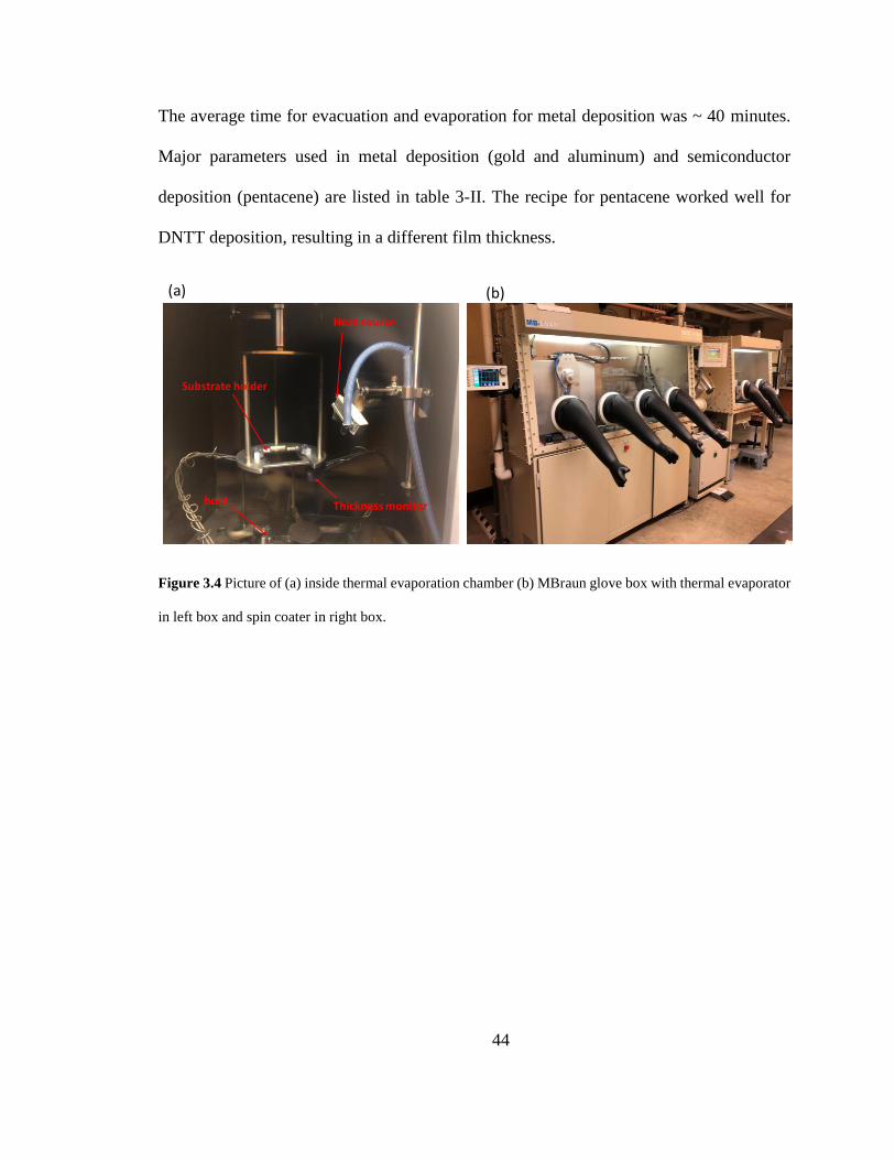
44
The average time for evacuation and evaporation for metal deposition was ~ 40 minutes.
Major parameters used in metal deposition (gold and aluminum) and semiconductor
deposition (pentacene) are listed in table 3-II. The recipe for pentacene worked well for
DNTT deposition, resulting in a different film thickness.
Figure 3.4 Picture of (a) inside thermal evaporation chamber (b) MBraun glove box with thermal evaporator
in left box and spin coater in right box.
(a) (b)
Heat source
Substrate holder
Thickness monitorboat
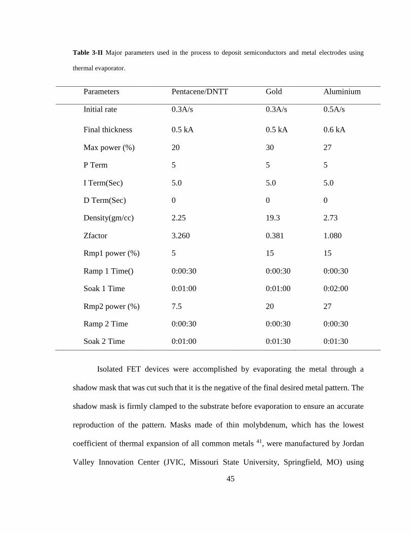
45
Table 3-II Major parameters used in the process to deposit semiconductors and metal electrodes using
thermal evaporator.
Isolated FET devices were accomplished by evaporating the metal through a
shadow mask that was cut such that it is the negative of the final desired metal pattern. The
shadow mask is firmly clamped to the substrate before evaporation to ensure an accurate
reproduction of the pattern. Masks made of thin molybdenum, which has the lowest
coefficient of thermal expansion of all common metals 41, were manufactured by Jordan
Valley Innovation Center (JVIC, Missouri State University, Springfield, MO) using
Parameters Pentacene/DNTT Gold Aluminium
Initial rate 0.3A/s 0.3A/s 0.5A/s
Final thickness 0.5 kA 0.5 kA 0.6 kA
Max power (%) 20 30 27
P Term 5 5 5
I Term(Sec) 5.0 5.0 5.0
D Term(Sec) 0 0 0
Density(gm/cc) 2.25 19.3 2.73
Zfactor 3.260 0.381 1.080
Rmp1 power (%) 5 15 15
Ramp 1 Time() 0:00:30 0:00:30 0:00:30
Soak 1 Time 0:01:00 0:01:00 0:02:00
Rmp2 power (%) 7.5 20 27
Ramp 2 Time 0:00:30 0:00:30 0:00:30
Soak 2 Time 0:01:00 0:01:30 0:01:30
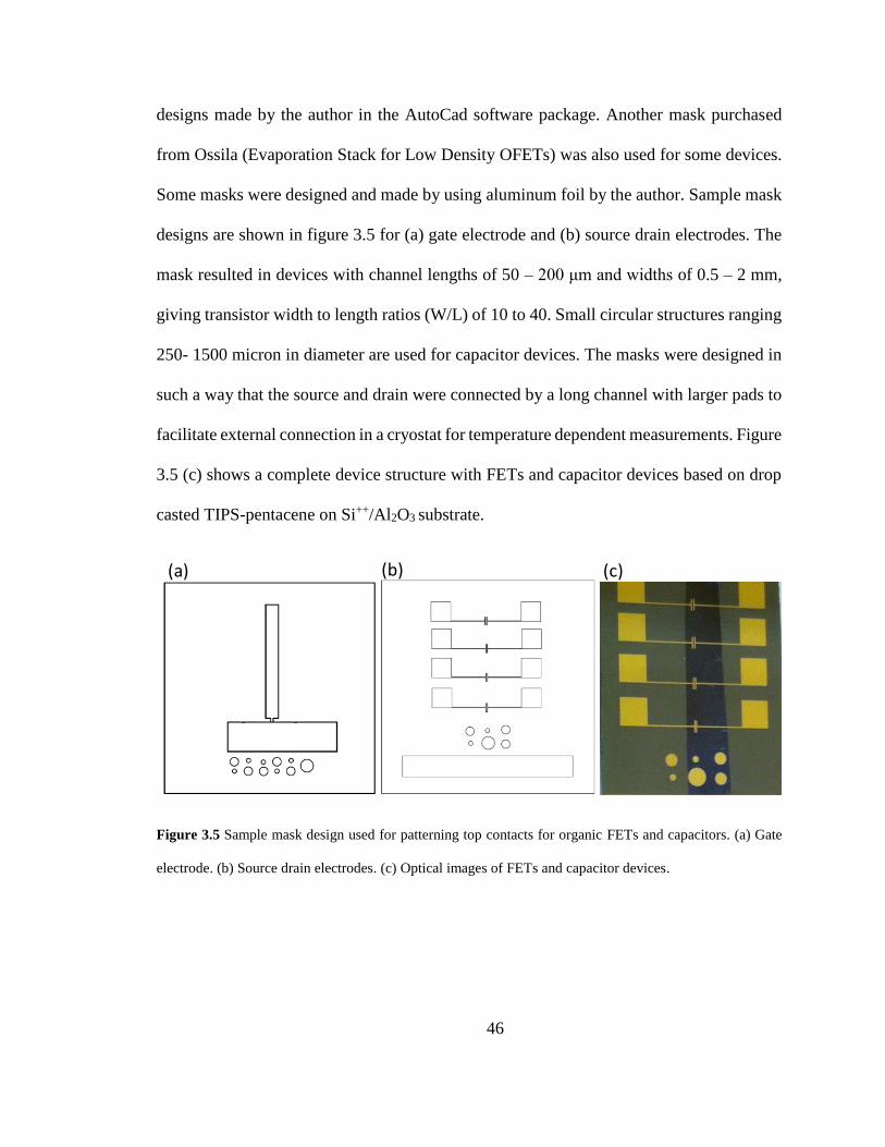
46
designs made by the author in the AutoCad software package. Another mask purchased
from Ossila (Evaporation Stack for Low Density OFETs) was also used for some devices.
Some masks were designed and made by using aluminum foil by the author. Sample mask
designs are shown in figure 3.5 for (a) gate electrode and (b) source drain electrodes. The
mask resulted in devices with channel lengths of 50 – 200 μm and widths of 0.5 – 2 mm,
giving transistor width to length ratios (W/L) of 10 to 40. Small circular structures ranging
250- 1500 micron in diameter are used for capacitor devices. The masks were designed in
such a way that the source and drain were connected by a long channel with larger pads to
facilitate external connection in a cryostat for temperature dependent measurements. Figure
3.5 (c) shows a complete device structure with FETs and capacitor devices based on drop
casted TIPS-pentacene on Si++/Al2O3 substrate.
Figure 3.5 Sample mask design used for patterning top contacts for organic FETs and capacitors. (a) Gate
electrode. (b) Source drain electrodes. (c) Optical images of FETs and capacitor devices.
(a) (b) (c)
47
3.3 Characterization
3.3.1 Surface morphology
Surface morphology of the fabricated thin films was examined using atomic force
microscopy, scanning electron microscopy, and contact angle measurements.
3.3.1.1 Atomic force microscopy
In an atomic force microscope (AFM), a cantilever with a very fine tip is used to
probe the surface of materials with a resolution on the atomic scale. This technique
monitors the change in force between the tip and the surface using an optical probe and by
dragging a very sharp tip at the end of a flexible cantilever across the surface of the sample.
The tip is moved by a piezoelectric system with high precision while its position is recorded
using a laser focused on the back of the cantilever whose reflection is incident on a
photodiode detector that transforms the information to a 2D image. AFM can be performed
in 3 different operating modes: (1) contact mode where the force on the tip is held constant
as it drags across the surface and this force is monitored by the laser positioning system to
create the image. It is commonly used for hard surfaces; (2) non-contact where the tip
hovers over the surface and interacts using van der Waals and other weak forces; (3)
tapping mode; the tip is in contact with the surface only occasionally. In the tapping mode
the cantilever is provided a constant driving force where it oscillates near a resonance
frequency. The amplitude of oscillations is constantly monitored by the laser/photodiode
system. We have employed the tapping mode for all AFM images presented in this work
as our samples are soft organic compounds. Typical cantilever specifications we used had
a spring constant of 0.1 N/m, a 28 kHz resonant frequency, a length of 22 mm, a width of
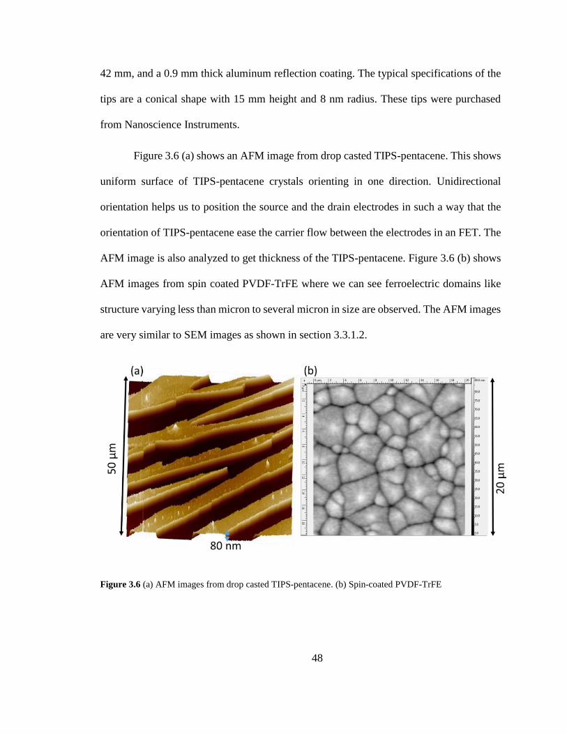
48
42 mm, and a 0.9 mm thick aluminum reflection coating. The typical specifications of the
tips are a conical shape with 15 mm height and 8 nm radius. These tips were purchased
from Nanoscience Instruments.
Figure 3.6 (a) shows an AFM image from drop casted TIPS-pentacene. This shows
uniform surface of TIPS-pentacene crystals orienting in one direction. Unidirectional
orientation helps us to position the source and the drain electrodes in such a way that the
orientation of TIPS-pentacene ease the carrier flow between the electrodes in an FET. The
AFM image is also analyzed to get thickness of the TIPS-pentacene. Figure 3.6 (b) shows
AFM images from spin coated PVDF-TrFE where we can see ferroelectric domains like
structure varying less than micron to several micron in size are observed. The AFM images
are very similar to SEM images as shown in section 3.3.1.2.
Figure 3.6 (a) AFM images from drop casted TIPS-pentacene. (b) Spin-coated PVDF-TrFE
49
3.3.1.2 Scanning electron microscopy
A scanning electron microscope (SEM) uses a non-invasive, nondestructive
technique often employed to examine the surface characteristics of materials in the
nanometer length scale. Here electrons are focused on the surface of the sample and they
interact with the sample. The scattered electrons are finally collected by a detector to form
an image. SEM is a sensitive tool to probe topography as well as the composition of the
sample surface. It consists of (1) an electron source, most commonly a field emission gun
or tungsten filament, that emits electrons in a beam. (2) One or two condenser lenses that
govern the intensity of the electron beam. (3) An objective lens that focuses the electron
beam on the surface of the sample. (4) Scanning coils that control the placement of the
beam. (5) An electron detector connected to the display. To limit the interaction of
electrons with ambient gas molecules, SEM is generally carried out under vacuum
conditions and the vacuum strength is adjusted according to the nature of the scanning
surface. A charging effect (found in insulating or poor conducting samples) tends to trap
electrons that do not escape from the sample surface and can cause bright spots in the
images. This prevents accurate reproduction of topography and limits the SEM
performance.
We used the Electron Microscopy (EM) Core facility at the University of Missouri,
Columbia and the SEM facility at the Department of Physics, University of the Western
Cape, South Africa. Low-voltage, secondary-electron micrographs of the film surface
morphology were collected with a Zeiss Auriga field-emission gun-scanning electron
microscope (FEG SEM) at an accelerating voltage of 1 keV as well as a FEI Scios Dual
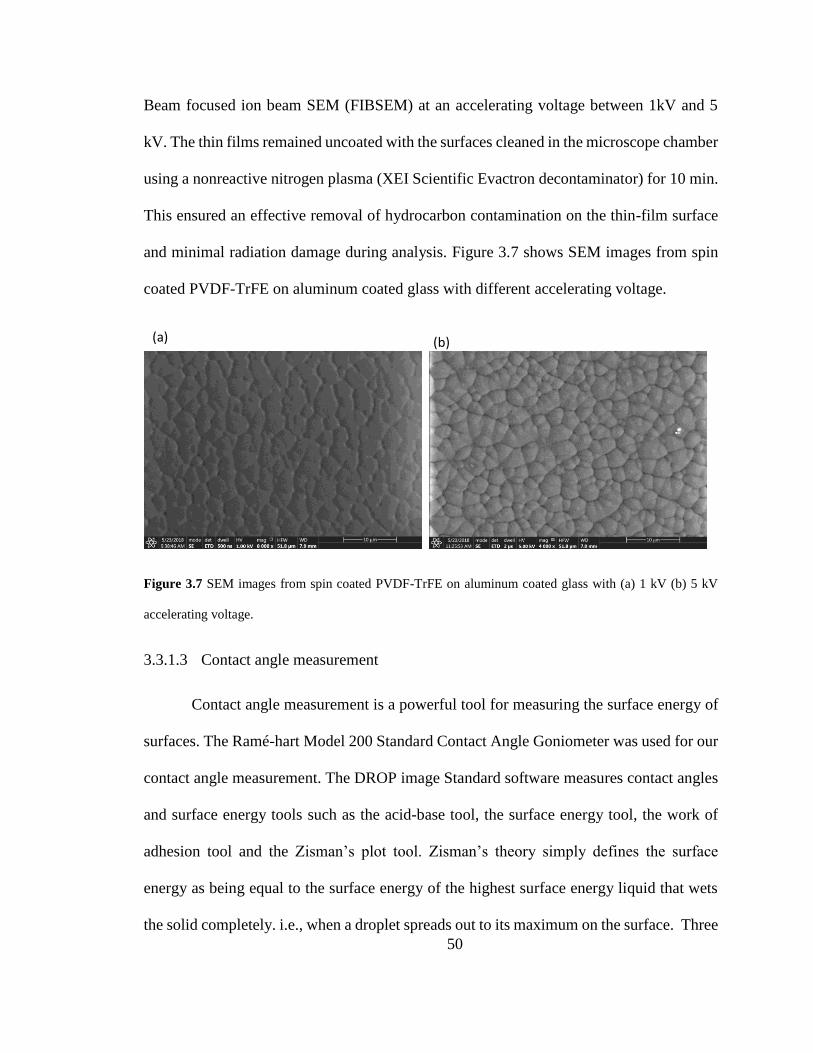
50
Beam focused ion beam SEM (FIBSEM) at an accelerating voltage between 1kV and 5
kV. The thin films remained uncoated with the surfaces cleaned in the microscope chamber
using a nonreactive nitrogen plasma (XEI Scientific Evactron decontaminator) for 10 min.
This ensured an effective removal of hydrocarbon contamination on the thin-film surface
and minimal radiation damage during analysis. Figure 3.7 shows SEM images from spin
coated PVDF-TrFE on aluminum coated glass with different accelerating voltage.
Figure 3.7 SEM images from spin coated PVDF-TrFE on aluminum coated glass with (a) 1 kV (b) 5 kV
accelerating voltage.
3.3.1.3 Contact angle measurement
Contact angle measurement is a powerful tool for measuring the surface energy of
surfaces. The Ramé-hart Model 200 Standard Contact Angle Goniometer was used for our
contact angle measurement. The DROP image Standard software measures contact angles
and surface energy tools such as the acid-base tool, the surface energy tool, the work of
adhesion tool and the Zisman’s plot tool. Zisman’s theory simply defines the surface
energy as being equal to the surface energy of the highest surface energy liquid that wets
the solid completely. i.e., when a droplet spreads out to its maximum on the surface. Three
(a) (b)
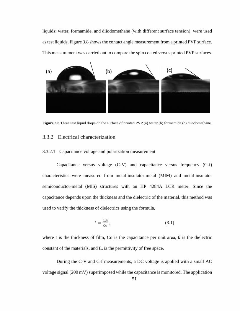
51
liquids: water, formamide, and diiodomethane (with different surface tension), were used
as test liquids. Figure 3.8 shows the contact angle measurement from a printed PVP surface.
This measurement was carried out to compare the spin coated versus printed PVP surfaces.
Figure 3.8 Three test liquid drops on the surface of printed PVP (a) water (b) formamide (c) diiodomethane.
3.3.2 Electrical characterization
3.3.2.1 Capacitance voltage and polarization measurement
Capacitance versus voltage (C-V) and capacitance versus frequency (C-f)
characteristics were measured from metal-insulator-metal (MIM) and metal-insulator
semiconductor-metal (MIS) structures with an HP 4284A LCR meter. Since the
capacitance depends upon the thickness and the dielectric of the material, this method was
used to verify the thickness of dielectrics using the formula,
𝑡 =Ԑ𝑜ƙ
𝐶𝑜 , (3.1)
where t is the thickness of film, Co is the capacitance per unit area, ƙ is the dielectric
constant of the materials, and Ԑo is the permittivity of free space.
During the C-V and C-f measurements, a DC voltage is applied with a small AC
voltage signal (200 mV) superimposed while the capacitance is monitored. The application
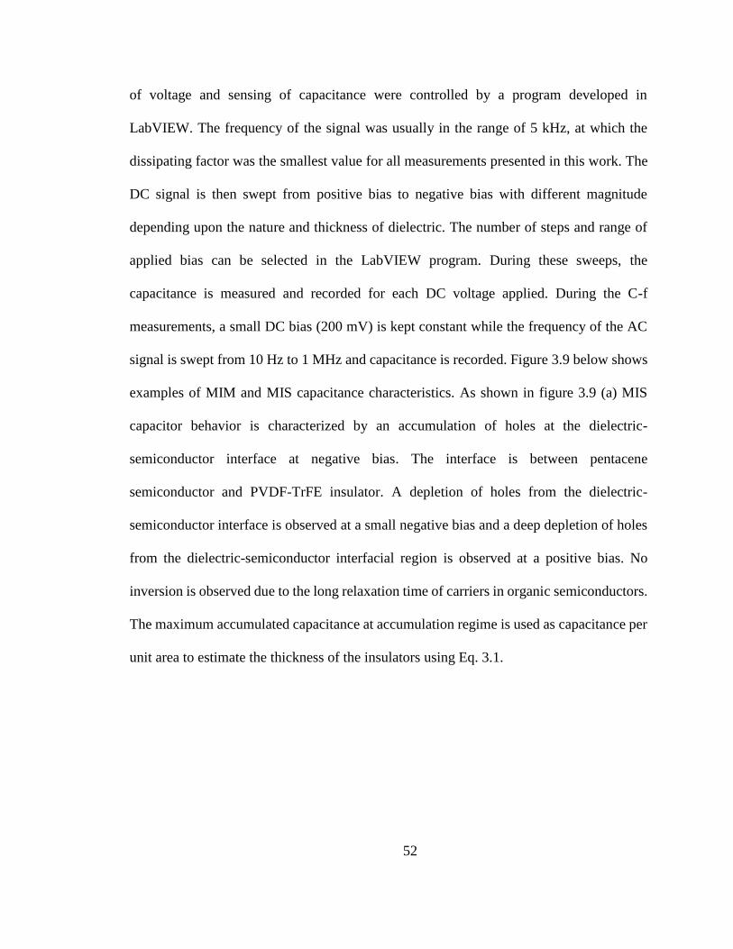
52
of voltage and sensing of capacitance were controlled by a program developed in
LabVIEW. The frequency of the signal was usually in the range of 5 kHz, at which the
dissipating factor was the smallest value for all measurements presented in this work. The
DC signal is then swept from positive bias to negative bias with different magnitude
depending upon the nature and thickness of dielectric. The number of steps and range of
applied bias can be selected in the LabVIEW program. During these sweeps, the
capacitance is measured and recorded for each DC voltage applied. During the C-f
measurements, a small DC bias (200 mV) is kept constant while the frequency of the AC
signal is swept from 10 Hz to 1 MHz and capacitance is recorded. Figure 3.9 below shows
examples of MIM and MIS capacitance characteristics. As shown in figure 3.9 (a) MIS
capacitor behavior is characterized by an accumulation of holes at the dielectric-
semiconductor interface at negative bias. The interface is between pentacene
semiconductor and PVDF-TrFE insulator. A depletion of holes from the dielectric-
semiconductor interface is observed at a small negative bias and a deep depletion of holes
from the dielectric-semiconductor interfacial region is observed at a positive bias. No
inversion is observed due to the long relaxation time of carriers in organic semiconductors.
The maximum accumulated capacitance at accumulation regime is used as capacitance per
unit area to estimate the thickness of the insulators using Eq. 3.1.
53
Figure 3.9 (a) MIS Capacitance-Voltage from Al/PVDF-TrFE/pentacene/Au structure. (b) MIM
Capacitance-frequency characteristics from Al/PVDF-TrFE/Al structure. (c) Dissipation factor from
Al/PVDF-TrFE/Al structure.
3.3.2.2 Current voltage measurement
The current-voltage (I-V) characteristics of the devices were measured by using
Keithley source meters 236, 2400, 2612B, and 4200. Keithley 236 and 2400 are single
source meters. For FET characterization we require the sourcing of two voltages (i.e. drain
voltage and gate voltage) and the measurement of the respective two currents, so the two
units were required to work in tandem. Keithley 2612B is a dual source meter which can
be used for sourcing and measurement simultaneously. The 2400 has a resolution of 10 nA
while the 236 and 2612B have a resolution of 100 fA. Source meter 4200 can measure as
low as 1 fA.
Room temperature transfer and output characteristics were recorded using a
LabVIEW program which set the 2400 to source the desired VGS while using a Keithley
236 to apply the desired VDS as it recorded the current. The program allowed us to choose
the desired start and end drain/gate voltage values along with the number of VDS/VGS points
101 102 103 104 105 1060.01
0.1
1
tan
d
Frequency (Hz)
30 nm PVDF-TrFE
101 102 103 104 105 106
160
200
240
Ca
pa
cita
nce
(n
F/c
m2)
Frequency (Hz)
30 nm PVDF-TrFE
(b) (c)
-3 -2 -1 0 1
0
100
200
300
400
Ca
pa
cita
nce
(n
F/c
m2)
Voltage (V)
20 nm PVDF-TrFE
(a)
54
to record allowing for a fully automated way to record a full set of output and transfer
characteristics.
For temperature-dependent electrical measurements, a dual source meter Keithley
2612B was used. Keithley 2612B has Test Script Processor (TSP) technology embedded
inside it and executes complete test programs. All temperature dependent transfer and
output characteristics were recorded with TSP. A standardized networking interface RJ-45
LAN crossover cable was used to connect the source meter and computer. As shown in the
photograph (figure 3.10) the organic FETs were kept inside a closed-cycle helium cryostat
(APD Cryogenics) where the temperature may be varied from 11K to 480 K. High vacuum
was obtained via TURBOTRONIK NT 10 (Ideal Vacuum) backed by a rotary vane pump
(Edwards) before starting the cooler. The temperature was measured using a Lakeshore
330 temperature controller. We allowed enough time to stabilize the temperature (typically
15 minutes from one measurement to another). Most of the devices were measured between
100K and 450 K. To test for reversibility, some devices were also measured from high
temperature to low temperature.
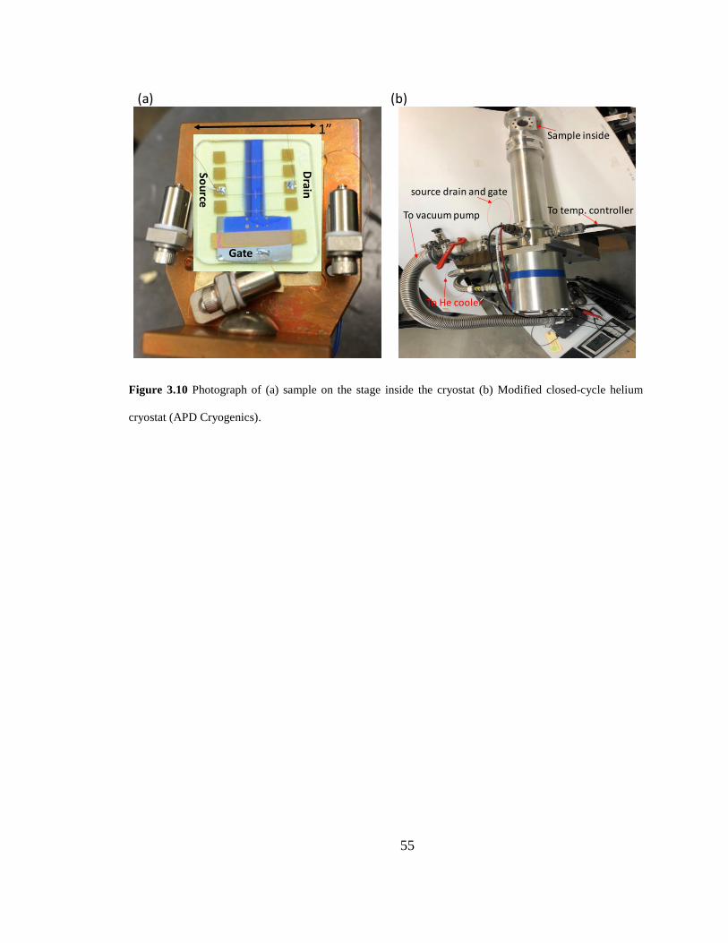
55
Figure 3.10 Photograph of (a) sample on the stage inside the cryostat (b) Modified closed-cycle helium
cryostat (APD Cryogenics).
1”
Sou
rce
Drain
Gate
(a) (b)
To temp. controller
Sample inside
To vacuum pump
To He cooler
source drain and gate
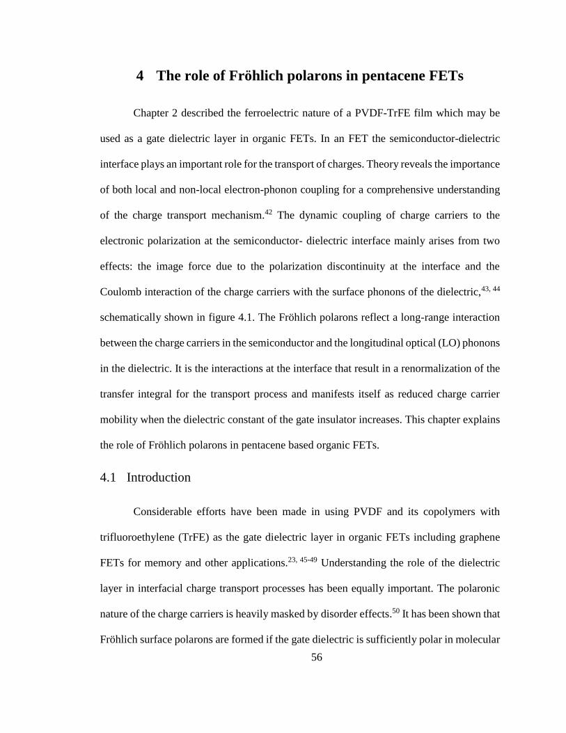
56
4 The role of Fröhlich polarons in pentacene FETs
Chapter 2 described the ferroelectric nature of a PVDF-TrFE film which may be
used as a gate dielectric layer in organic FETs. In an FET the semiconductor-dielectric
interface plays an important role for the transport of charges. Theory reveals the importance
of both local and non-local electron-phonon coupling for a comprehensive understanding
of the charge transport mechanism.42 The dynamic coupling of charge carriers to the
electronic polarization at the semiconductor- dielectric interface mainly arises from two
effects: the image force due to the polarization discontinuity at the interface and the
Coulomb interaction of the charge carriers with the surface phonons of the dielectric,43, 44
schematically shown in figure 4.1. The Fröhlich polarons reflect a long-range interaction
between the charge carriers in the semiconductor and the longitudinal optical (LO) phonons
in the dielectric. It is the interactions at the interface that result in a renormalization of the
transfer integral for the transport process and manifests itself as reduced charge carrier
mobility when the dielectric constant of the gate insulator increases. This chapter explains
the role of Fröhlich polarons in pentacene based organic FETs.
4.1 Introduction
Considerable efforts have been made in using PVDF and its copolymers with
trifluoroethylene (TrFE) as the gate dielectric layer in organic FETs including graphene
FETs for memory and other applications.23, 45-49 Understanding the role of the dielectric
layer in interfacial charge transport processes has been equally important. The polaronic
nature of the charge carriers is heavily masked by disorder effects.50 It has been shown that
Fröhlich surface polarons are formed if the gate dielectric is sufficiently polar in molecular
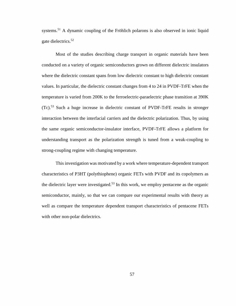
57
systems.51 A dynamic coupling of the Fröhlich polarons is also observed in ionic liquid
gate dielectrics.52
Most of the studies describing charge transport in organic materials have been
conducted on a variety of organic semiconductors grown on different dielectric insulators
where the dielectric constant spans from low dielectric constant to high dielectric constant
values. In particular, the dielectric constant changes from 4 to 24 in PVDF-TrFE when the
temperature is varied from 200K to the ferroelectric-paraelectric phase transition at 390K
(Tc).53 Such a huge increase in dielectric constant of PVDF-TrFE results in stronger
interaction between the interfacial carriers and the dielectric polarization. Thus, by using
the same organic semiconductor-insulator interface, PVDF-TrFE allows a platform for
understanding transport as the polarization strength is tuned from a weak-coupling to
strong-coupling regime with changing temperature.
This investigation was motivated by a work where temperature-dependent transport
characteristics of P3HT (polythiophene) organic FETs with PVDF and its copolymers as
the dielectric layer were investigated.53 In this work, we employ pentacene as the organic
semiconductor, mainly, so that we can compare our experimental results with theory as
well as compare the temperature dependent transport characteristics of pentacene FETs
with other non-polar dielectrics.
58
Figure 4.1 Schematic of a ferroelectric-based FET where the dynamic coupling of charge carriers to the
electronic polarization at the semiconductor-dielectric interface is illustrated. In addition to the bulk disorder
within the semiconductor, there is trapping of charges at the interface.
4.2 Comparison of polar versus non-polar dielectric
Thermally activated transport in pentacene organic FETs using non-ferroelectric
dielectrics has been observed by many groups.54-56 Other acene-based semiconductors also
show activated transport with a distinct relationship between the contact-induced film
microstructure and charge carrier mobility.57 Since pentacene has many grain boundaries,
rather than a bandlike transport, a thermally activated hopping of charges from site to site
within a disorder-induced exponential distribution of states, as proposed by Monroe58, is
observed. In such a mechanism, the charge carrier mobility, µFET, is given by,
µ𝐹𝐸𝑇 = µ𝑜exp(−
∆
𝑘𝐵𝑇), (4.1)
++
+ +
P(VDF)
P(TrFE)
N(E)
E
59
where ∆, the activation energy, is the energetic difference between the Fermi energy and
the transport level, µo is the mobility in the absence of any trap states, and kB is the
Boltzmann constant. Additionally, as the charge carrier density increases, the Fermi energy
gets closer to the transport level, easing the transport of charges; thus decreasing ∆. Within
the context of transport in organic FETs, the above model is more complex, especially
when the polarization field of the dielectric interface needs to be considered. By comparing
PVDF-TrFE-based organic FET characteristics to non-polar dielectric organic FETs, the
effect of the polarization field can be readily observed.
Figure 4.2 (a) Transfer curves at different temperatures from 100K to 350K for a pentacene FET with PMMA
as the dielectric layer. (b) Transfer curves at different temperatures from 200K to 440K for a pentacene FET
with PVDF-TrFE as the dielectric layer. In both cases, VDS=-4V.
Figure 4.2 shows the transconductance curves of PMMA and PVDF-TrFE organic
FETs at various temperatures. In both cases, each of transfer curves was measured at a 10
K interval of temperature in the saturation regime.
-4 -3 -2 -1 0
0.0
0.4
0.8
1.2
PVDF-TrFE (130nm)
200 K
I DS(
A)
VGS
(V)
440 K
-4 -3 -2 -1 0
0.0
0.1
0.2
350 K
I DS (
A
)
VGS
(V)
PMMA (150nm)
100 K
(a) (b)
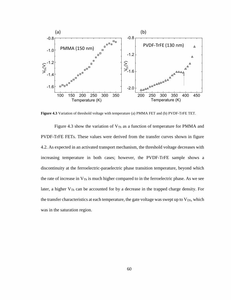
60
Figure 4.3 Variation of threshold voltage with temperature (a) PMMA FET and (b) PVDF-TrFE TET.
Figure 4.3 show the variation of VTh as a function of temperature for PMMA and
PVDF-TrFE FETs. These values were derived from the transfer curves shown in figure
4.2. As expected in an activated transport mechanism, the threshold voltage decreases with
increasing temperature in both cases; however, the PVDF-TrFE sample shows a
discontinuity at the ferroelectric-paraelectric phase transition temperature, beyond which
the rate of increase in VTh is much higher compared to in the ferroelectric phase. As we see
later, a higher VTh can be accounted for by a decrease in the trapped charge density. For
the transfer characteristics at each temperature, the gate voltage was swept up to VDS, which
was in the saturation region.
200 250 300 350 400 450
-2.0
-1.6
-1.2
-0.8
Vth(V
)
Temperature (K)100 150 200 250 300 350
-1.6
-1.4
-1.2
-1.0
-0.8
Vth(V
)
Temperature (K)
(a) (b)
PMMA (150 nm)PVDF-TrFE (130 nm)
Th
Th
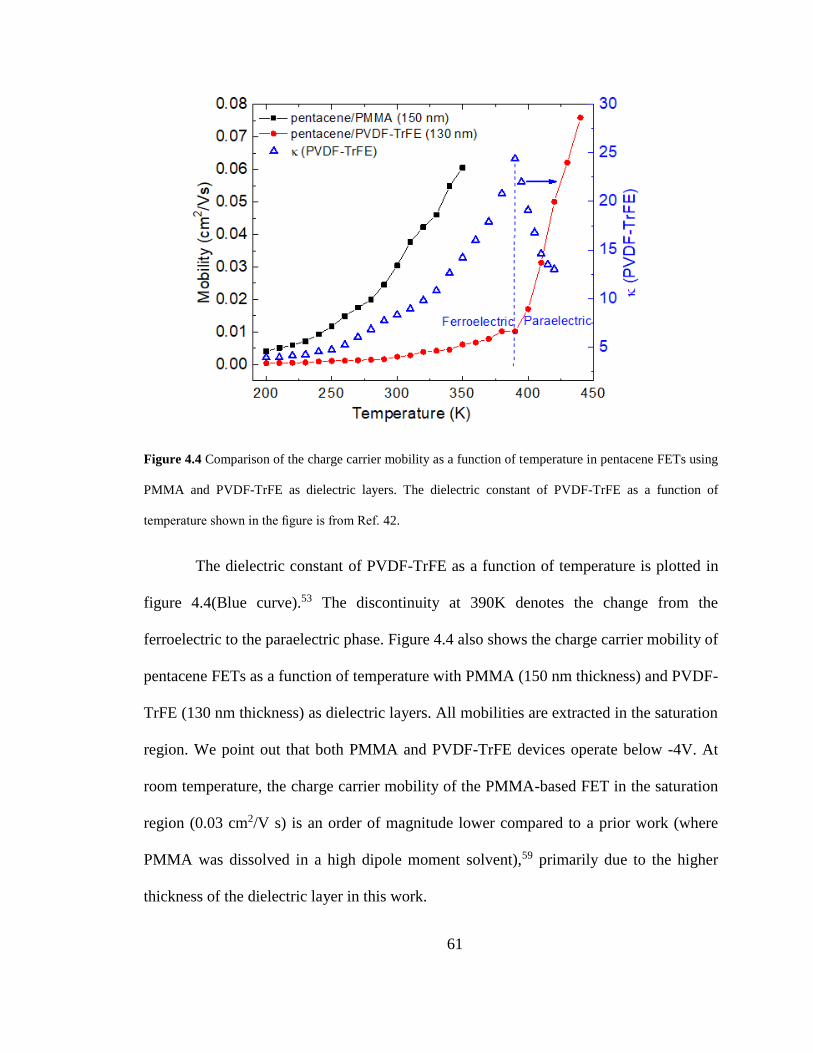
61
Figure 4.4 Comparison of the charge carrier mobility as a function of temperature in pentacene FETs using
PMMA and PVDF-TrFE as dielectric layers. The dielectric constant of PVDF-TrFE as a function of
temperature shown in the figure is from Ref. 42.
The dielectric constant of PVDF-TrFE as a function of temperature is plotted in
figure 4.4(Blue curve).53 The discontinuity at 390K denotes the change from the
ferroelectric to the paraelectric phase. Figure 4.4 also shows the charge carrier mobility of
pentacene FETs as a function of temperature with PMMA (150 nm thickness) and PVDF-
TrFE (130 nm thickness) as dielectric layers. All mobilities are extracted in the saturation
region. We point out that both PMMA and PVDF-TrFE devices operate below -4V. At
room temperature, the charge carrier mobility of the PMMA-based FET in the saturation
region (0.03 cm2/V s) is an order of magnitude lower compared to a prior work (where
PMMA was dissolved in a high dipole moment solvent),59 primarily due to the higher
thickness of the dielectric layer in this work.
62
Since PMMA degrades at higher temperatures, the pentacene/PMMA FET
measurements were carried out only up to 350 K. The PVDF-TrFE-based FETs were
tracked all the way from the ferroelectric phase to above Tc. Agreeably, the charge carrier
density may differ at the two dielectric interfaces but there are clear differences in the
nature of carrier mobility versus temperature in the two devices. The PMMA device shows
a sharp increase in its mobility with increasing temperature, whereas the PVDF-TrFE
device shows a suppressed mobility in the ferroelectric phase, beyond which there is a large
change in its mobility.
The suppression of the charge carrier mobility with increasing temperature in the
ferroelectric phase may be attributed to a coupling of the charge carriers to the dielectric
polarization of the gate insulator, resulting in a renormalization of the transfer integral, J.
The dynamic coupling thus reduces J to J*, thereby increasing the effective mass (m*) of
the carriers. Theoretical calculations show that m* increases by a factor of 1.27 in bulk
pentacene due to molecular polarization effects.44 In order to understand whether there is
a universality in the dynamical coupling due to the polarization effect and to distinguish
between surface and bulk effects, we have carried out detailed temperature dependent
current-voltage (I-V) measurements from pentacene FETs by varying the thickness of the
PVDF-TrFE layer. These results are presented in the next section.
4.3 Thickness-dependence of the ferroelectric layer
The thickness of the PVDF-TrFE layer was varied from 20nm to 500 nm; the
pentacene layer thickness was kept the same at 60 nm for all FETs. All devices show a
similar trend for charge carrier mobilities versus temperature as shown in figure 4.4, where
63
µFET shows a sharp increase beyond the ferroelectric-paraelectric phase transition at 390
K. Figure 4.5 shows the Arrhenius plots of FET mobilities in the ferroelectric phase for
varying thicknesses of the PVDF-TrFE layer. The 20 nm device (not shown here) shows
an activation energy of 88 meV. We note that the activation energies (∆) obtained by fits
to Eq. (4.1), are much higher here than typically seen for pentacene FETs with non-
ferroelectric dielectrics.56 Furthermore, the correction due to thermalization of individual
dipoles (as a result of the nonlinear contribution) when the system approaches Tc has not
been taken into account here.53 Taking this correction may slightly reduce the mobility in
the ferroelectric phase, thus further enhancing ∆. Since the FETs in this work are low
operating voltage devices, the nonlinear contribution may not be that high as evident from
a prior work on polarization measurements from PVDF-TrFE capacitors with similar
thicknesses.60
The trend in Figure 4.4 clearly shows the activation energy to decrease with
increasing thickness of the dielectric layer. This observation is consistent with slightly
higher values of µFET for thicker layers of PVDF-TrFE. In the ferroelectric region, there
are thus two competing effects: activated hopping transport, which tends to increase µFET
with increasing temperatures, and the coupling of the carriers to the electric polarization in
the form of surface Fröhlich polarons as ƙ increases with temperature, which tends to
decrease µFET. The thinner dielectric layers induce stronger polarization fields, suppressing
the charge carrier mobility even more compared to the thicker dielectric layers in the
ferroelectric region.
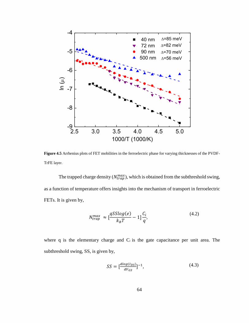
64
Figure 4.5 Arrhenius plots of FET mobilities in the ferroelectric phase for varying thicknesses of the PVDF-
TrFE layer.
The trapped charge density (𝑁𝑡𝑟𝑎𝑝𝑚𝑎𝑥), which is obtained from the subthreshold swing,
as a function of temperature offers insights into the mechanism of transport in ferroelectric
FETs. It is given by,
𝑁𝑡𝑟𝑎𝑝𝑚𝑎𝑥 ≈ [
𝑞𝑆𝑆𝑙𝑜𝑔(𝑒)
𝑘𝐵𝑇− 1]
𝐶𝑖𝑞,
(4.2)
where q is the elementary charge and Ci is the gate capacitance per unit area. The
subthreshold swing, SS, is given by,
𝑆𝑆 = [𝑑𝑙𝑜𝑔(𝐼𝐷𝑆)
𝑑𝑉𝐺𝑆]−1, (4.3)
2.5 3.0 3.5 4.0 4.5 5.0-9
-8
-7
-6
-5
-4
=82 meV
=56 meV
=70 meV
40 nm
72 nm
90 nm
500 nmln
()
1000/T (1000/K)
=85 meV
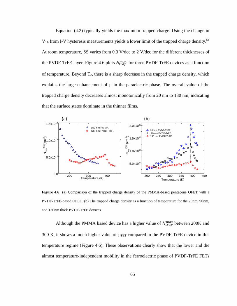
65
Equation (4.2) typically yields the maximum trapped charge. Using the change in
VTh from I-V hysteresis measurements yields a lower limit of the trapped charge density.61
At room temperature, SS varies from 0.3 V/dec to 2 V/dec for the different thicknesses of
the PVDF-TrFE layer. Figure 4.6 plots 𝑁𝑡𝑟𝑎𝑝𝑚𝑎𝑥 for three PVDF-TrFE devices as a function
of temperature. Beyond Tc, there is a sharp decrease in the trapped charge density, which
explains the large enhancement of µ in the paraelectric phase. The overall value of the
trapped charge density decreases almost monotonically from 20 nm to 130 nm, indicating
that the surface states dominate in the thinner films.
Figure 4.6 (a) Comparison of the trapped charge density of the PMMA-based pentacene OFET with a
PVDF-TrFE-based OFET. (b) The trapped charge density as a function of temperature for the 20nm, 90nm,
and 130nm thick PVDF-TrFE devices.
Although the PMMA based device has a higher value of 𝑁𝑡𝑟𝑎𝑝𝑚𝑎𝑥 between 200K and
300 K, it shows a much higher value of µFET compared to the PVDF-TrFE device in this
temperature regime (Figure 4.6). These observations clearly show that the lower and the
almost temperature-independent mobility in the ferroelectric phase of PVDF-TrFE FETs
200 250 300 350 400 450
5.0x10¹²
1.0x10¹³
1.5x10¹³
2.0x10¹³N
tra
pm
ax (
cm
-2)
Temperature (K)
20 nm PVDF-TrFE
90 nm PVDF-TrFE
130 nm PVDF-TrFE
200 300 4000.0
5.0x10¹²
1.0x10¹³
1.5x10¹³
Ntr
apm
ax(c
m-2
)
Temperature (K)
150 nm PMMA
130 nm PVDF-TrFE
(a) (b)
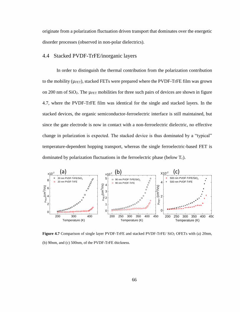
66
originate from a polarization fluctuation driven transport that dominates over the energetic
disorder processes (observed in non-polar dielectrics).
4.4 Stacked PVDF-TrFE/inorganic layers
In order to distinguish the thermal contribution from the polarization contribution
to the mobility (µFET), stacked FETs were prepared where the PVDF-TrFE film was grown
on 200 nm of SiO2. The µFET mobilities for three such pairs of devices are shown in figure
4.7, where the PVDF-TrFE film was identical for the single and stacked layers. In the
stacked devices, the organic semiconductor-ferroelectric interface is still maintained, but
since the gate electrode is now in contact with a non-ferroelectric dielectric, no effective
change in polarization is expected. The stacked device is thus dominated by a “typical”
temperature-dependent hopping transport, whereas the single ferroelectric-based FET is
dominated by polarization fluctuations in the ferroelectric phase (below Tc).
Figure 4.7 Comparison of single layer PVDF-TrFE and stacked PVDF-TrFE/ SiO2 OFETs with (a) 20nm,
(b) 90nm, and (c) 500nm, of the PVDF-TrFE thickness.
200 300 400
0
2
4
6
8
x10-2
F
ET(c
m2/V
s)
Temperature (K)
20 nm PVDF-TrFE/SiO2
20 nm PVDF-TrFE
200 250 300 350 400 450
0
2
4
500 nm PVDF-TrFE/SiO2
500 nm PVDF-TrFE
F
ET (
cm
2/V
s)
Temperature (K)
X10-2
200 250 300 350 400 450
0
1
2
3
4
5
x10-2
F
ET(c
m2/V
s)
Temperature (K)
90 nm PVDF-TrFE/SiO2
90 nm PVDF-TrFE
(a) (b) (c)
67
Assuming that the ferroelectric component of the stacked device contributes
negligibly to transport, the mobility (µstack) as a function of temperature may be used as a
reference to take into account the contribution from all additional factors. By using the
Matthiessen’s rule,
µ𝐹𝐸𝑇 = [1
µ𝑃+
1
µ𝑠𝑡𝑎𝑐𝑘]−1, (4.4)
the contribution due to the Fröhlich polarons, µP, may be extracted from the knowledge of
the temperature dependence of the mobility of single layer ferroelectric and stacked
devices. The strongly coupled Fröhlich polaron model27 yields,
µ𝑃(𝑇) =𝑒𝑎2𝜔𝑆
8𝑘𝐵𝑇exp (−
∆𝑃
𝑘𝐵𝑇), (4.5)
where ωS is the frequency of the surface phonons of the dielectric, a is the hopping length,
and ∆P is the polaron hopping barrier. We note that ωS is related to the longitudinal (ωL)
and transverse (ωT) optical phonon frequencies by,
𝜔𝑆2 =
1
2(𝜔𝐿
2 − 𝜔𝑇2), (4.6)
The factor of 8 in the denominator of Eq. 4.5 results from considering an upper bound to
the mobility in the hopping process. The Einstein’s relation for a nondegenerate carrier gas
yields µ =𝑞𝐷
𝑘𝑘𝐵𝑇, where D, the diffusion coefficient, is given by γa2/4 in two-dimensional
hopping motion, and γ is the hopping rate. The probability of hopping takes on a factor of
1/2 for each attempt to pass the barrier in the forward direction. Figure 4.8 shows the
temperature-dependent mobility of Fröhlich polarons for FETs with 500 nm, 90 nm, and
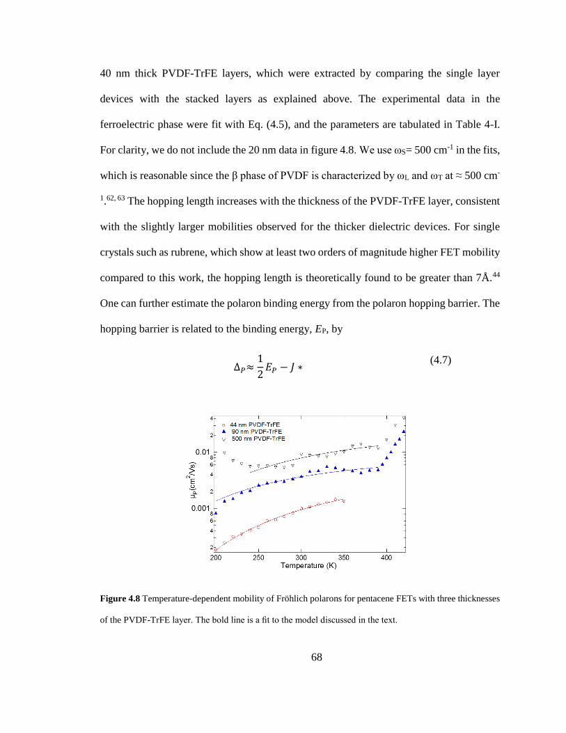
68
40 nm thick PVDF-TrFE layers, which were extracted by comparing the single layer
devices with the stacked layers as explained above. The experimental data in the
ferroelectric phase were fit with Eq. (4.5), and the parameters are tabulated in Table 4-I.
For clarity, we do not include the 20 nm data in figure 4.8. We use ωS= 500 cm-1 in the fits,
which is reasonable since the β phase of PVDF is characterized by ωL and ωT at ≈ 500 cm-
1.62, 63 The hopping length increases with the thickness of the PVDF-TrFE layer, consistent
with the slightly larger mobilities observed for the thicker dielectric devices. For single
crystals such as rubrene, which show at least two orders of magnitude higher FET mobility
compared to this work, the hopping length is theoretically found to be greater than 7Å.44
One can further estimate the polaron binding energy from the polaron hopping barrier. The
hopping barrier is related to the binding energy, EP, by
∆𝑃≈
1
2𝐸𝑃 − 𝐽 ∗
(4.7)
Figure 4.8 Temperature-dependent mobility of Fröhlich polarons for pentacene FETs with three thicknesses
of the PVDF-TrFE layer. The bold line is a fit to the model discussed in the text.
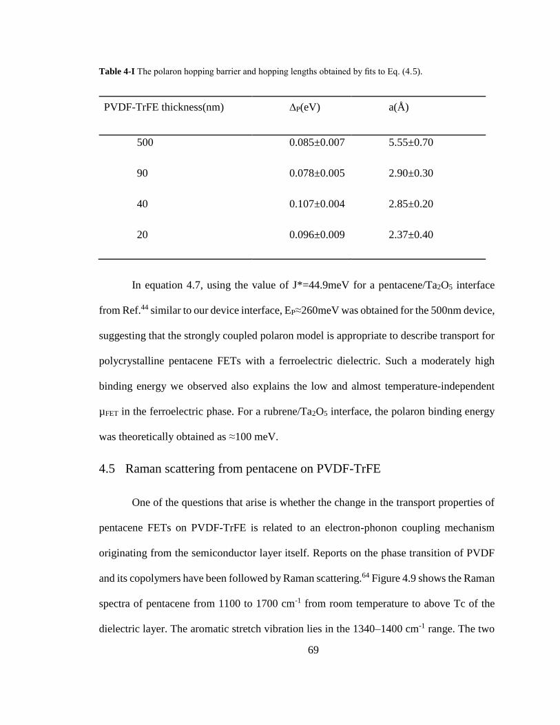
69
Table 4-I The polaron hopping barrier and hopping lengths obtained by fits to Eq. (4.5).
PVDF-TrFE thickness(nm) ∆P(eV) a(Å)
500 0.085±0.007 5.55±0.70
90 0.078±0.005 2.90±0.30
40 0.107±0.004 2.85±0.20
20 0.096±0.009 2.37±0.40
In equation 4.7, using the value of J*=44.9meV for a pentacene/Ta2O5 interface
from Ref.44 similar to our device interface, EP≈260meV was obtained for the 500nm device,
suggesting that the strongly coupled polaron model is appropriate to describe transport for
polycrystalline pentacene FETs with a ferroelectric dielectric. Such a moderately high
binding energy we observed also explains the low and almost temperature-independent
µFET in the ferroelectric phase. For a rubrene/Ta2O5 interface, the polaron binding energy
was theoretically obtained as ≈100 meV.
4.5 Raman scattering from pentacene on PVDF-TrFE
One of the questions that arise is whether the change in the transport properties of
pentacene FETs on PVDF-TrFE is related to an electron-phonon coupling mechanism
originating from the semiconductor layer itself. Reports on the phase transition of PVDF
and its copolymers have been followed by Raman scattering.64 Figure 4.9 shows the Raman
spectra of pentacene from 1100 to 1700 cm-1 from room temperature to above Tc of the
dielectric layer. The aromatic stretch vibration lies in the 1340–1400 cm-1 range. The two
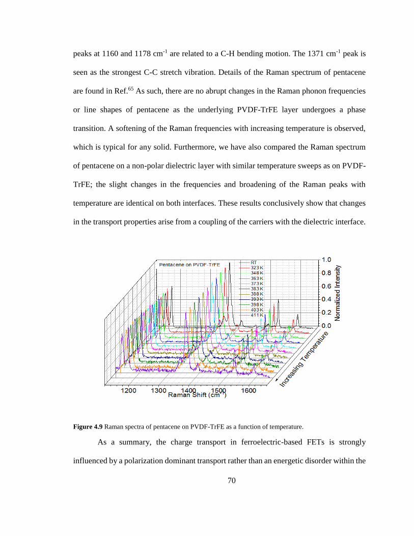
70
peaks at 1160 and 1178 cm-1 are related to a C-H bending motion. The 1371 cm-1 peak is
seen as the strongest C-C stretch vibration. Details of the Raman spectrum of pentacene
are found in Ref.65 As such, there are no abrupt changes in the Raman phonon frequencies
or line shapes of pentacene as the underlying PVDF-TrFE layer undergoes a phase
transition. A softening of the Raman frequencies with increasing temperature is observed,
which is typical for any solid. Furthermore, we have also compared the Raman spectrum
of pentacene on a non-polar dielectric layer with similar temperature sweeps as on PVDF-
TrFE; the slight changes in the frequencies and broadening of the Raman peaks with
temperature are identical on both interfaces. These results conclusively show that changes
in the transport properties arise from a coupling of the carriers with the dielectric interface.
Figure 4.9 Raman spectra of pentacene on PVDF-TrFE as a function of temperature.
As a summary, the charge transport in ferroelectric-based FETs is strongly
influenced by a polarization dominant transport rather than an energetic disorder within the
71
framework of a hopping transport. The ferroelectric dielectric, PVDF-TrFE, which shows
a large change in its dielectric constant as the temperature is swept from 200 K to the
ferroelectric paraelectric phase transition temperature at 390 K, provides a testbed to study
interfacial transport as the polarization strength is tuned. When the gate insulator is
sufficiently polar, Fröhlich polarons play an important role in interfacial transport.
Temperature-dependent charge carrier mobility in pentacene FETs shows almost no
change as long as the dielectric layer is in the ferroelectric phase due to the coupling of the
charge carriers with the surface phonons of the dielectric layer. This effect is more
pronounced for thinner dielectric films. The threshold voltage and the trapped charge
density also show a discontinuity at the ferroelectric paraelectric phase transition. To
extract the polarization contribution to the temperature dependence of the charge carrier
mobility from mechanisms other than Fröhlich polarons, ideally one should look at a
pentacene FET where the gate insulator is vacuum. This is clearly not an option for a
polycrystalline film such as pentacene. The bilayer (SiO2/PVDF-TrFE) devices show a
typical temperature-dependent mobility as seen with non-polar dielectrics. Temperature-
dependent mobility was extracted by comparing the bilayer devices with single layer
PVDF-TrFE pentacene FETs. Using a strongly coupled Fröhlich polaron model, we
estimate the hopping length and the hopping barrier of the polarons. The hopping lengths
vary between 2 Å and 5 Å.
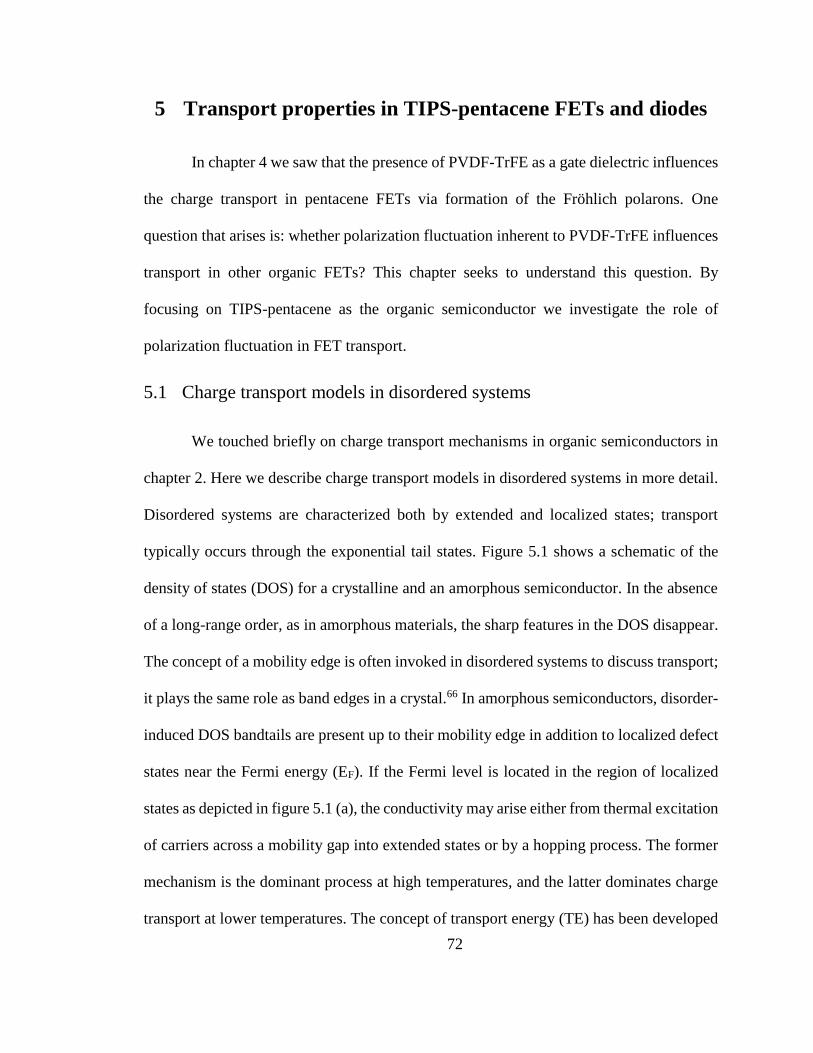
72
5 Transport properties in TIPS-pentacene FETs and diodes
In chapter 4 we saw that the presence of PVDF-TrFE as a gate dielectric influences
the charge transport in pentacene FETs via formation of the Fröhlich polarons. One
question that arises is: whether polarization fluctuation inherent to PVDF-TrFE influences
transport in other organic FETs? This chapter seeks to understand this question. By
focusing on TIPS-pentacene as the organic semiconductor we investigate the role of
polarization fluctuation in FET transport.
5.1 Charge transport models in disordered systems
We touched briefly on charge transport mechanisms in organic semiconductors in
chapter 2. Here we describe charge transport models in disordered systems in more detail.
Disordered systems are characterized both by extended and localized states; transport
typically occurs through the exponential tail states. Figure 5.1 shows a schematic of the
density of states (DOS) for a crystalline and an amorphous semiconductor. In the absence
of a long-range order, as in amorphous materials, the sharp features in the DOS disappear.
The concept of a mobility edge is often invoked in disordered systems to discuss transport;
it plays the same role as band edges in a crystal.66 In amorphous semiconductors, disorder-
induced DOS bandtails are present up to their mobility edge in addition to localized defect
states near the Fermi energy (EF). If the Fermi level is located in the region of localized
states as depicted in figure 5.1 (a), the conductivity may arise either from thermal excitation
of carriers across a mobility gap into extended states or by a hopping process. The former
mechanism is the dominant process at high temperatures, and the latter dominates charge
transport at lower temperatures. The concept of transport energy (TE) has been developed
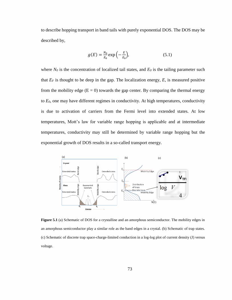
73
to describe hopping transport in band tails with purely exponential DOS. The DOS may be
described by,
𝑔(𝐸) =𝑁0
𝐸0exp (−
𝐸
𝐸0), (5.1)
where N0 is the concentration of localized tail states, and E0 is the tailing parameter such
that EF is thought to be deep in the gap. The localization energy, E, is measured positive
from the mobility edge (E = 0) towards the gap center. By comparing the thermal energy
to E0, one may have different regimes in conductivity. At high temperatures, conductivity
is due to activation of carriers from the Fermi level into extended states. At low
temperatures, Mott’s law for variable range hopping is applicable and at intermediate
temperatures, conductivity may still be determined by variable range hopping but the
exponential growth of DOS results in a so-called transport energy.
Figure 5.1 (a) Schematic of DOS for a crystalline and an amorphous semiconductor. The mobility edges in
an amorphous semiconductor play a similar role as the band edges in a crystal. (b) Schematic of trap states.
(c) Schematic of discrete trap space-charge-limited conduction in a log-log plot of current density (J) versus
voltage.
(a) (b) (c)
74
The concept of transport energy was introduced by Monroe in terms of a non-
equilibrium energy relaxation problem where the electrons directly hop between localized,
bandtail states.58 Starting from the mobility edge, the electrons hop downward in energy.
This relaxation process changes at some particular energy represented as the transport
energy (TE). The hopping process near and below this energy resembles dispersive
transport with TE playing the same role as the mobility edge.
The hopping rate of electrons between localized states may be described by Miller
Abraham's formalism 67,
𝜈𝑖𝑗 = 𝜈0exp (−2𝑅𝑖𝑗
𝛼−(𝐸𝑖−𝐸𝑗+|𝐸𝑗−𝐸𝑖|)
𝑘𝐵𝑇), (5.2)
In Eq. (5.2), νij is the rate of hopping between an occupied site i (with energy Ei)
and an empty state j (with energy Ej), separated by a distance Rij; α is the decay length of
the wave function; ν0 is the attempt-to-hop or attempt-to-escape frequency. Since the
decreasing DOS makes it difficult for a charge carrier to find a neighbor at low energies,
carriers in deep states move by thermal excitation to shallower states, whilst carriers in
shallow states move by hopping to other shallow states.
Organic and polymeric semiconductors are usually characterized by a Gaussian
DOS rather than the exponential bandtail discussed earlier. The rationale is that the
distribution of disordered potential leads to electron localization, which is Gaussian.
Although one can invoke the concept of TE with Gaussian DOS, an exact analytical form
is not possible. Furthermore, the concept of TE in organic semiconductors provides a
reasonable description of variable range hopping, where transport is via hopping in the
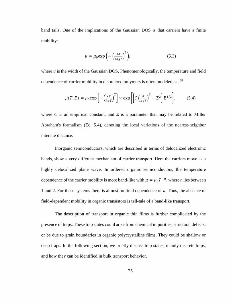
75
band tails. One of the implications of the Gaussian DOS is that carriers have a finite
mobility:
𝜇 = 𝜇0exp (−(2𝜎
3𝑘𝐵𝑇)2
), (5.3)
where σ is the width of the Gaussian DOS. Phenomenologically, the temperature and field
dependence of carrier mobility in disordered polymers is often modeled as: 68
𝜇(𝑇, 𝐸) = 𝜇0exp [− (2𝜎
𝑘𝐵𝑇)2
] × exp [[𝐶 (𝜎
𝑘𝐵𝑇)2
− Σ2] 𝐸1/2], (5.4)
where C is an empirical constant, and Σ is a parameter that may be related to Miller
Abraham's formalism (Eq. 5.4), denoting the local variations of the nearest-neighbor
intersite distance.
Inorganic semiconductors, which are described in terms of delocalized electronic
bands, show a very different mechanism of carrier transport. Here the carriers move as a
highly delocalized plane wave. In ordered organic semiconductors, the temperature
dependence of the carrier mobility is more band-like with 𝜇 = 𝜇0𝑇−𝑛, where n lies between
1 and 2. For these systems there is almost no field dependence of μ. Thus, the absence of
field-dependent mobility in organic transistors is tell-tale of a band-like transport.
The description of transport in organic thin films is further complicated by the
presence of traps. These trap states could arise from chemical impurities, structural defects,
or be due to grain boundaries in organic polycrystalline films. They could be shallow or
deep traps. In the following section, we briefly discuss trap states, mainly discrete traps,
and how they can be identified in bulk transport behavior.
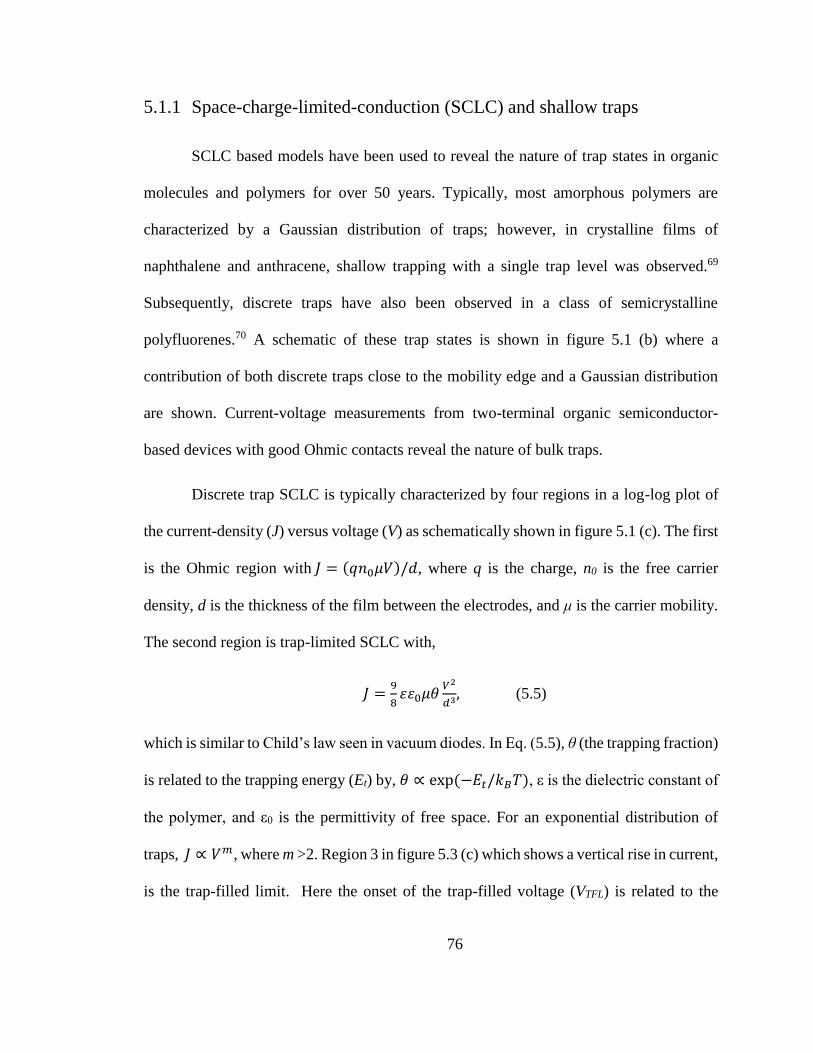
76
5.1.1 Space-charge-limited-conduction (SCLC) and shallow traps
SCLC based models have been used to reveal the nature of trap states in organic
molecules and polymers for over 50 years. Typically, most amorphous polymers are
characterized by a Gaussian distribution of traps; however, in crystalline films of
naphthalene and anthracene, shallow trapping with a single trap level was observed.69
Subsequently, discrete traps have also been observed in a class of semicrystalline
polyfluorenes.70 A schematic of these trap states is shown in figure 5.1 (b) where a
contribution of both discrete traps close to the mobility edge and a Gaussian distribution
are shown. Current-voltage measurements from two-terminal organic semiconductor-
based devices with good Ohmic contacts reveal the nature of bulk traps.
Discrete trap SCLC is typically characterized by four regions in a log-log plot of
the current-density (J) versus voltage (V) as schematically shown in figure 5.1 (c). The first
is the Ohmic region with 𝐽 = (𝑞𝑛0𝜇𝑉)/𝑑, where q is the charge, n0 is the free carrier
density, d is the thickness of the film between the electrodes, and μ is the carrier mobility.
The second region is trap-limited SCLC with,
𝐽 =9
8𝜀𝜀0𝜇𝜃
𝑉2
𝑑3, (5.5)
which is similar to Child’s law seen in vacuum diodes. In Eq. (5.5), θ (the trapping fraction)
is related to the trapping energy (Et) by, 𝜃 ∝ exp (−𝐸𝑡/𝑘𝐵𝑇), ε is the dielectric constant of
the polymer, and ε0 is the permittivity of free space. For an exponential distribution of
traps, 𝐽 ∝ 𝑉𝑚, where m >2. Region 3 in figure 5.3 (c) which shows a vertical rise in current,
is the trap-filled limit. Here the onset of the trap-filled voltage (VTFL) is related to the
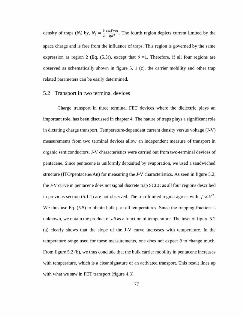
77
density of traps (Nt) by, 𝑁𝑡 =3
2
𝜀𝜀0𝑉𝑇𝐹𝐿
𝑞𝑑2. The fourth region depicts current limited by the
space charge and is free from the influence of traps. This region is governed by the same
expression as region 2 (Eq. (5.5)), except that θ =1. Therefore, if all four regions are
observed as schematically shown in figure 5. 1 (c), the carrier mobility and other trap
related parameters can be easily determined.
5.2 Transport in two terminal devices
Charge transport in three terminal FET devices where the dielectric plays an
important role, has been discussed in chapter 4. The nature of traps plays a significant role
in dictating charge transport. Temperature-dependent current density versus voltage (J-V)
measurements from two terminal devices allow an independent measure of transport in
organic semiconductors. J-V characteristics were carried out from two-terminal devices of
pentacene. Since pentacene is uniformly deposited by evaporation, we used a sandwiched
structure (ITO/pentacene/Au) for measuring the J-V characteristics. As seen in figure 5.2,
the J-V curve in pentacene does not signal discrete trap SCLC as all four regions described
in previous section (5.1.1) are not observed. The trap-limited region agrees with 𝐽 ∝ 𝑉2.
We thus use Eq. (5.5) to obtain bulk μ at all temperatures. Since the trapping fraction is
unknown, we obtain the product of μθ as a function of temperature. The inset of figure 5.2
(a) clearly shows that the slope of the J-V curve increases with temperature. In the
temperature range used for these measurements, one does not expect θ to change much.
From figure 5.2 (b), we thus conclude that the bulk carrier mobility in pentacene increases
with temperature, which is a clear signature of an activated transport. This result lines up
with what we saw in FET transport (figure 4.3).
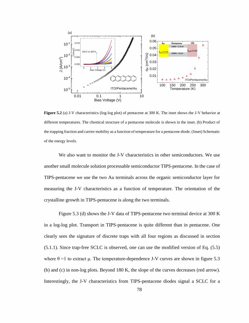
78
Figure 5.2 (a) J-V characteristics (log-log plot) of pentacene at 300 K. The inset shows the J-V behavior at
different temperatures. The chemical structure of a pentacene molecule is shown in the inset. (b) Product of
the trapping fraction and carrier mobility as a function of temperature for a pentacene diode. (Inset) Schematic
of the energy levels.
We also want to monitor the J-V characteristics in other semiconductors. We use
another small molecule solution processable semiconductor TIPS-pentacene. In the case of
TIPS-pentacene we use the two Au terminals across the organic semiconductor layer for
measuring the J-V characteristics as a function of temperature. The orientation of the
crystalline growth in TIPS-pentacene is along the two terminals.
Figure 5.3 (d) shows the J-V data of TIPS-pentacene two terminal device at 300 K
in a log-log plot. Transport in TIPS-pentacene is quite different than in pentacene. One
clearly sees the signature of discrete traps with all four regions as discussed in section
(5.1.1). Since trap-free SCLC is observed, one can use the modified version of Eq. (5.5)
where θ =1 to extract μ. The temperature-dependence J-V curves are shown in figure 5.3
(b) and (c) in non-log plots. Beyond 180 K, the slope of the curves decreases (red arrow).
Interestingly, the J-V characteristics from TIPS-pentacene diodes signal a SCLC for a
0.01 0.1 1 10
10-5
10-4
10-3
10-2
10-1
0 1 2 3 4
0.000
0.005
0.010
0.015
J (
A/c
m2)
Bias Voltage (V)
100 K to 300 K
J (
A/c
m2)
Bias Voltage (V)
ITO/Pentacene/Au100 150 200 250 300
0.01
0.02
0.03
0.04
0.05
0.06
ITO/Pentacene/Au
(cm
2/V
s)
Temperature (K)
Au Pentacene ITO
EF Au= 5.1 eV
LUMO = 2.70 eV
HOMO = 4.9 eV
EF ITO= 4.7 eV
(a)(b)
79
discrete set of trap levels, suggesting that charge injection and transport occur through
regions of ordering in the semiconductor. By using the same region for the trap-free SCLC
at all temperatures, the bulk carrier mobility (μbulk) is extracted, as plotted in the inset of
figure 5.3 (d). A clear decrease in μbulk is observed beyond 180 K.
Figure 5.3 (a) Chemical structure of TIPS-pentacene and an optical image from a TIPS-pentacene device.
(b) and (c) J-V curves from a TIPS-pentacene two-terminal device as a function of temperature. (d) J-V curve
(log-log plot) at 300 K showing all four regions, characteristics of discrete trap SCLC. Inset shows the bulk
carrier mobilities as a function of temperature.
In comparing pentacene to TIPS-pentacene, we found that the J-V diode
characteristics are quite different: TIPS-pentacene, which shows discrete trap SCLC, yields
a decreasing mobility beyond a certain temperature. The origin of the shallow discrete traps
in TIPS-pentacene could be structural or due to other chemical defects and may occur at
grain boundaries. Pentacene, on the other hand, which is characterized by a distribution of
0 5 10 15 20 25 30 35
0.000
0.001
0.002
0.003
0.004 100 K
120 K
140 K
160 K
180 K
J (
A/c
m2)
Bias Voltage (V)
0 5 10 15 20 25 30 35
0.000
0.001
0.002
0.003
0.004 180 K
200 K
220 K
260 K
280 K
300 K
J (
A/c
m2)
Bias Voltage (V)
300 K
(a)
(b)
(c)
(d)
0.1 1 1010-6
10-5
10-4
10-3
10-2
10-1
100 200 300
0.2
0.4
(
cm
2/V
s)
Temperature (K)
Au/TIPS-pentacene/Au
SCLC
trap-free
SCLC
trap-limited
J (
A/c
m2)
Bias Voltage (V)
Au/TIPS-pentacene/AuOhmic
VTFL
trap-filled
80
traps, yields an activated transport with increasing bulk μ as a function of increasing
temperature, in agreement with FET transport as discussed in chapter 4.
5.3 Role of dielectrics in charge transport
The field of organic FETs has seen an increasing usage in polymer dielectric
materials and a progressively lower dependence on traditional oxide dielectrics, such as
SiO2 and Al2O3. Much effort has gone into modification of the dielectric interface;
appropriate gate dielectrics that are free of electron-trapping groups, such as hydroxyl or
silanol, have allowed the demonstration of n-channel FETs.71 In order to achieve stable and
low-operating voltage FETs, the dielectric surface should be hydrophobic and must provide
a relatively high capacitance, which is often a challenge with polymer dielectrics as they
have an inherently low value of κ. However, using techniques for lowering the thickness
of polymer dielectrics, high capacitance may be achieved.
As discussed in chapter 4, Fröhlich polarons are observed in molecular
semiconductor based FETs when the gate dielectric is sufficiently polar.51 A consequence
of such an interaction would be lower carrier mobility. Thus, one would expect that as κ of
the dielectric medium increases, the FET carrier mobility should decrease. The polarization
field of a ferroelectric dielectric should have an additional contribution to the carrier
mobility. As an example, we plot the FET carrier mobilities of TIPS-pentacene FETs at
300 K for various polymer and inorganic dielectrics used in our study (Figure 5.4). Figure
5.4 (a-c) shows the various FET geometries used in our work, where either a top or a bottom
gate dielectric geometry has been used. CYTOP (κ = 2) is extremely hydrophobic; hence
it is easier to use it as top gate dielectric rather than a bottom gate dielectric. We will later
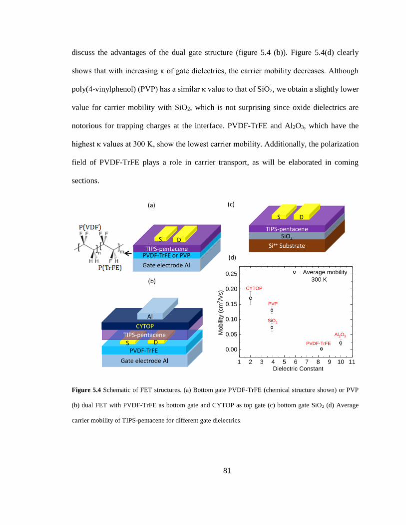
81
discuss the advantages of the dual gate structure (figure 5.4 (b)). Figure 5.4(d) clearly
shows that with increasing κ of gate dielectrics, the carrier mobility decreases. Although
poly(4-vinylphenol) (PVP) has a similar κ value to that of SiO2, we obtain a slightly lower
value for carrier mobility with SiO2, which is not surprising since oxide dielectrics are
notorious for trapping charges at the interface. PVDF-TrFE and Al2O3, which have the
highest κ values at 300 K, show the lowest carrier mobility. Additionally, the polarization
field of PVDF-TrFE plays a role in carrier transport, as will be elaborated in coming
sections.
Figure 5.4 Schematic of FET structures. (a) Bottom gate PVDF-TrFE (chemical structure shown) or PVP
(b) dual FET with PVDF-TrFE as bottom gate and CYTOP as top gate (c) bottom gate SiO2 (d) Average
carrier mobility of TIPS-pentacene for different gate dielectrics.
(c)
Si++ Substrate
SiO2
TIPS-pentacene
S D
Gate electrode Al
PVDF-TrFES D
TIPS-pentacene
CYTOP
Al
(b)
(a)
Gate electrode Al
PVDF-TrFE or PVPTIPS-pentacene
S D
(d)
1 2 3 4 5 6 7 8 9 10 11
0.00
0.05
0.10
0.15
0.20
0.25
Al2O3
PVDF-TrFE
SiO2
PVP
Average mobility
300 K
Mo
bili
ty (
cm
2/V
s)
Dielectric Constant
CYTOP
82
5.4 Carrier transport in TIPS-pentacene FETs
In section 5.2 we saw that the bulk transport in pentacene and TIPS-pentacene are
quite different. Furthermore, TIPS-pentacene shows an unusual property similar to single
crystals, where the mobility decreases with increase in temperature, which led us to
investigate the temperature dependent transport in TIPS-pentacene.
In single-crystal organic FETs such as rubrene, the disorder is significantly reduced,
enabling the realization of intrinsic polaronic transport, including the observation of the
Hall effect in the accumulation layer.72 The Hall voltage is a sensitive probe that measures
the extent of delocalized adiabatic transport. The presence of the normal Hall effect in
organic FETs is, therefore, a signature that the surface charge is similar to a two-
dimensional hole or an electron-gas system rather than a hopping of carriers.73
There have been several recent works that show band-like transport, characterized
by a negative coefficient of the charge-carrier μ with respect to temperature (T) (dμ/dT <
0), in solution-processable small-molecule and polymer-based FETs. In TIPS-pentacene a
negative coefficient of the carrier mobility at high electric fields was attributed to localized
transport limited by thermal-lattice fluctuation.12 In a few acene-based solution-
processable small molecule FETs, charge delocalization induced by the dynamic disorder
as a function of temperature has been probed by charge-modulation spectroscopy, shedding
light on the nature of shallow traps.74 By incorporating large thermal-lattice fluctuations
with weak van der Waals intermolecular bonding, theoretical models have explained the
band-like motion observed at high temperatures from highly conducting organic
semiconductors.75 In such materials, the carriers diffuse incoherently in the presence of
83
the large thermal fluctuations, resulting in a weakly metallic behavior. Band-like transport
in TIPS-pentacene FETs has also been observed by time-resolved optical second-
harmonic-generation imaging.76 A common feature for dμ/dT < 0 to occur beyond a certain
temperature, as seen across a variety of organic semiconductors, is that the FET carrier
mobility should be larger than μmin = er2/2ℏ, where r is the intermolecular distance, e is the
electronic charge, and ℏ is the Planck’s constant.77 Typically, this condition translates to
FET mobilities being greater than 1 to 2 cm2/Vs, ensuring that the energy bandwidth is
larger than the energy change involved in the scattering. Recently, ac Hall Effect
measurements have shed light on the coexistence of both band-like and hopping charge
carriers in the accumulation region of organic FETs. Because of this mixed transport
regime, even when FET carrier mobilities are less than 1 cm2/Vs, a Hall voltage is
measurable.78, 79 It may be prudent to point out that band-like transport in molecular
semiconductors, which mainly occurs in narrow bands, is somewhat different from true
band transport, where the latter occurs through extended states in perfect crystals.
In pure organic crystals such as naphthalene, band transport for electrons was
observed below 150 K .80 Subsequently, first-principles calculations involving inter- and
intramolecular vibrations and electron-phonon coupling constants (both local and
nonlocal) have elucidated band-to-hopping transition in naphthalene as a function of
temperature.81 This transition can be understood on the basis of localization of charge
carriers in the absence of any thermal disorder. Furthermore, at the transition where the
charges are more delocalized, raising the temperature destroys the translational symmetry
and reduces the charge transport efficiency, and thus its mobility.82 The apparent band-like
transport observed as dμ/dT < 0 in organic and polymeric FETs may be mediated by
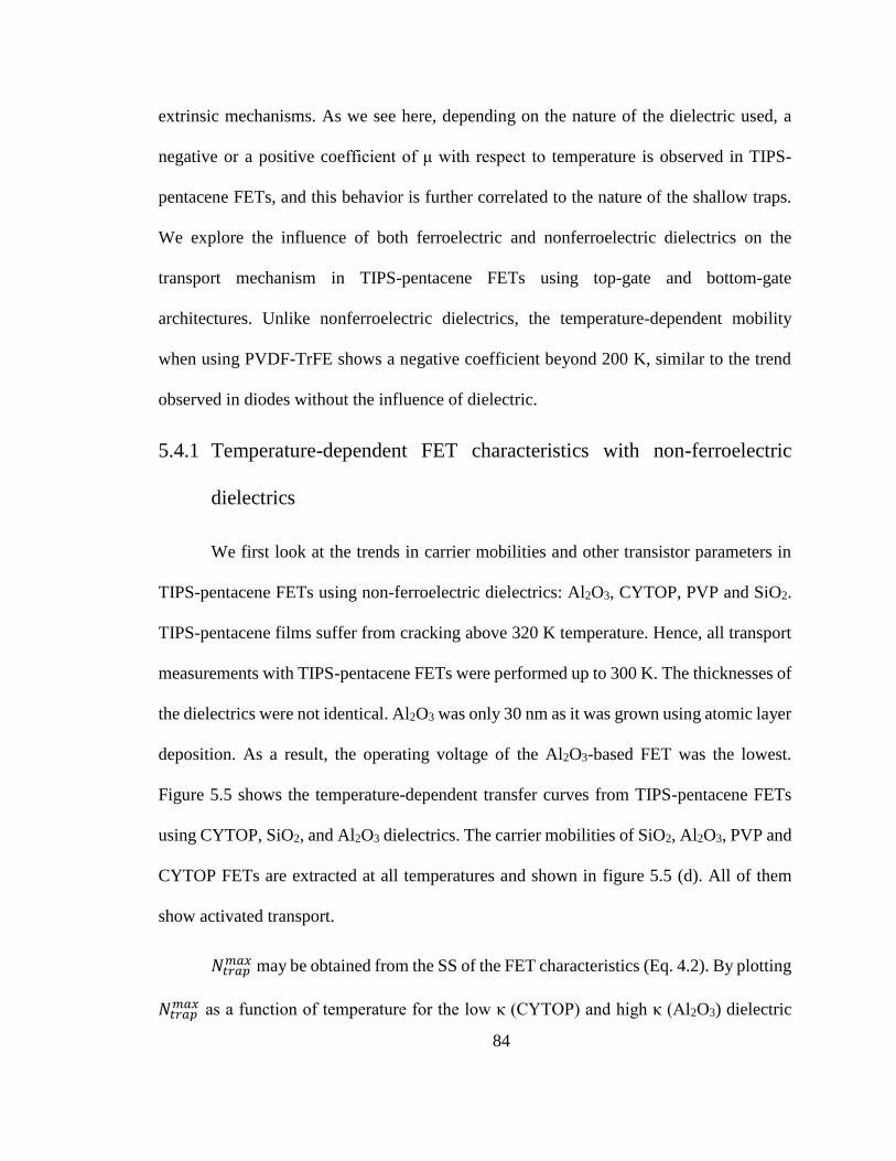
84
extrinsic mechanisms. As we see here, depending on the nature of the dielectric used, a
negative or a positive coefficient of μ with respect to temperature is observed in TIPS-
pentacene FETs, and this behavior is further correlated to the nature of the shallow traps.
We explore the influence of both ferroelectric and nonferroelectric dielectrics on the
transport mechanism in TIPS-pentacene FETs using top-gate and bottom-gate
architectures. Unlike nonferroelectric dielectrics, the temperature-dependent mobility
when using PVDF-TrFE shows a negative coefficient beyond 200 K, similar to the trend
observed in diodes without the influence of dielectric.
5.4.1 Temperature-dependent FET characteristics with non-ferroelectric
dielectrics
We first look at the trends in carrier mobilities and other transistor parameters in
TIPS-pentacene FETs using non-ferroelectric dielectrics: Al2O3, CYTOP, PVP and SiO2.
TIPS-pentacene films suffer from cracking above 320 K temperature. Hence, all transport
measurements with TIPS-pentacene FETs were performed up to 300 K. The thicknesses of
the dielectrics were not identical. Al2O3 was only 30 nm as it was grown using atomic layer
deposition. As a result, the operating voltage of the Al2O3-based FET was the lowest.
Figure 5.5 shows the temperature-dependent transfer curves from TIPS-pentacene FETs
using CYTOP, SiO2, and Al2O3 dielectrics. The carrier mobilities of SiO2, Al2O3, PVP and
CYTOP FETs are extracted at all temperatures and shown in figure 5.5 (d). All of them
show activated transport.
𝑁𝑡𝑟𝑎𝑝𝑚𝑎𝑥 may be obtained from the SS of the FET characteristics (Eq. 4.2). By plotting
𝑁𝑡𝑟𝑎𝑝𝑚𝑎𝑥 as a function of temperature for the low κ (CYTOP) and high κ (Al2O3) dielectric
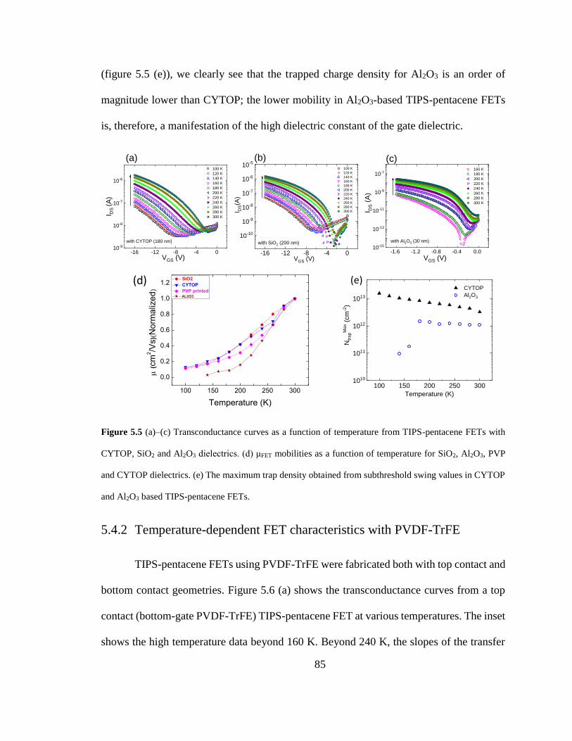
85
(figure 5.5 (e)), we clearly see that the trapped charge density for Al2O3 is an order of
magnitude lower than CYTOP; the lower mobility in Al2O3-based TIPS-pentacene FETs
is, therefore, a manifestation of the high dielectric constant of the gate dielectric.
Figure 5.5 (a)–(c) Transconductance curves as a function of temperature from TIPS-pentacene FETs with
CYTOP, SiO2 and Al2O3 dielectrics. (d) μFET mobilities as a function of temperature for SiO2, Al2O3, PVP
and CYTOP dielectrics. (e) The maximum trap density obtained from subthreshold swing values in CYTOP
and Al2O3 based TIPS-pentacene FETs.
5.4.2 Temperature-dependent FET characteristics with PVDF-TrFE
TIPS-pentacene FETs using PVDF-TrFE were fabricated both with top contact and
bottom contact geometries. Figure 5.6 (a) shows the transconductance curves from a top
contact (bottom-gate PVDF-TrFE) TIPS-pentacene FET at various temperatures. The inset
shows the high temperature data beyond 160 K. Beyond 240 K, the slopes of the transfer
-16 -12 -8 -4 0
10-10
10-9
10-8
10-7
10-6
10-5
with SiO2 (200 nm)
100 K
120 K
140 K
160 K
180 K
200 K
220 K
240 K
260 K
280 K
300 KI DS(A
)
VGS (V)-1.6 -1.2 -0.8 -0.4 0.0
10-15
10-13
10-11
10-9
10-7
with Al2O3 (30 nm)
160 K
180 K
200 K
220 K
240 K
260 K
280 K
300 K
I DS (
A)
VGS (V)
(c)
-16 -12 -8 -4 010-9
10-8
10-7
10-6
with CYTOP (180 nm)
100 K
120 K
140 K
160 K
180 K
200 K
220 K
240 K
260 K
280 K
300 K
I DS
(A
)
VGS (V)
(b)(a)
80 120 160 200 240 280 3200
50
100
150x10-3
(
cm
2/V
s)
SiO2
Al2O3
CYTOP
Temperature (K)
x10-3
0
10
20
(d)
100 150 200 250 3001010
1011
1012
1013
CYTOP
Al2O3
Ntr
ap
Ma
x (
cm
-2)
Temperature (K)
(e)-16 -12 -8 -4 0
10-10
10-9
10-8
10-7
10-6
10-5
with SiO2 (200 nm)
100 K
120 K
140 K
160 K
180 K
200 K
220 K
240 K
260 K
280 K
300 KI DS(A
)
VGS (V)-1.6 -1.2 -0.8 -0.4 0.0
10-15
10-13
10-11
10-9
10-7
with Al2O3 (30 nm)
160 K
180 K
200 K
220 K
240 K
260 K
280 K
300 K
I DS (
A)
VGS (V)
(c)
-16 -12 -8 -4 010-9
10-8
10-7
10-6
with CYTOP (180 nm)
100 K
120 K
140 K
160 K
180 K
200 K
220 K
240 K
260 K
280 K
300 K
I DS
(A
)
VGS (V)
(b)(a)
80 120 160 200 240 280 3200
50
100
150x10-3
(
cm
2/V
s)
SiO2
Al2O3
CYTOP
Temperature (K)
x10-3
0
10
20
(d)
100 150 200 250 3001010
1011
1012
1013
CYTOP
Al2O3
Ntr
ap
Ma
x (
cm
-2)
Temperature (K)
(e)(d)
100 150 200 250 300
0.0
0.2
0.4
0.6
0.8
1.0
1.2
(cm
2/V
s)(N
orm
aliz
ed
)
Temperature (K)
SiO2
CYTOP
PVP printed AL2O3
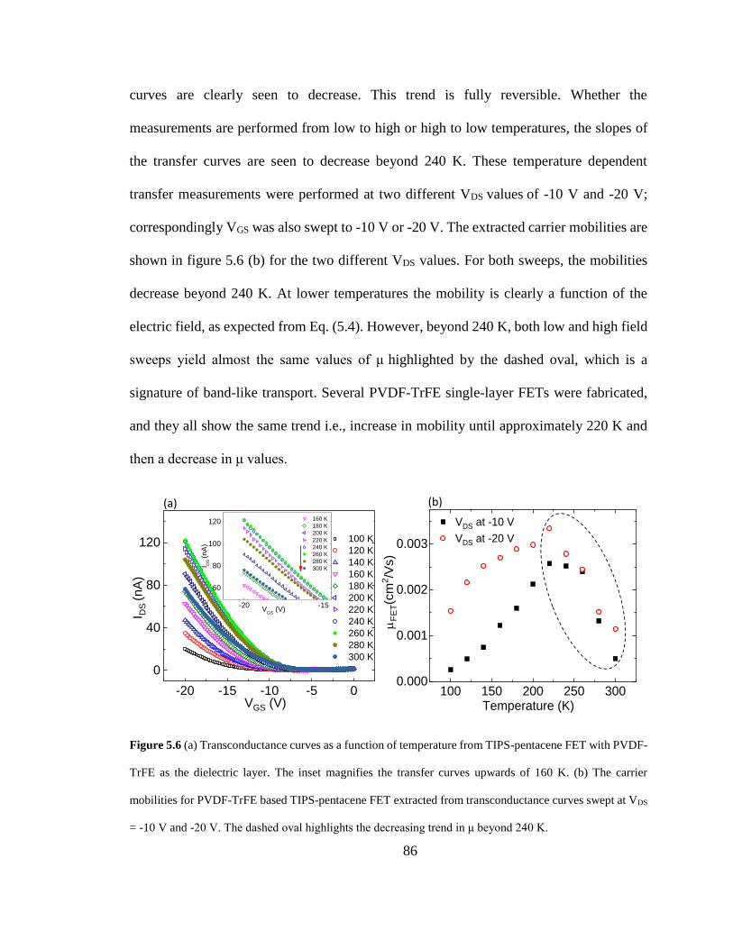
86
curves are clearly seen to decrease. This trend is fully reversible. Whether the
measurements are performed from low to high or high to low temperatures, the slopes of
the transfer curves are seen to decrease beyond 240 K. These temperature dependent
transfer measurements were performed at two different VDS values of -10 V and -20 V;
correspondingly VGS was also swept to -10 V or -20 V. The extracted carrier mobilities are
shown in figure 5.6 (b) for the two different VDS values. For both sweeps, the mobilities
decrease beyond 240 K. At lower temperatures the mobility is clearly a function of the
electric field, as expected from Eq. (5.4). However, beyond 240 K, both low and high field
sweeps yield almost the same values of μ highlighted by the dashed oval, which is a
signature of band-like transport. Several PVDF-TrFE single-layer FETs were fabricated,
and they all show the same trend i.e., increase in mobility until approximately 220 K and
then a decrease in μ values.
Figure 5.6 (a) Transconductance curves as a function of temperature from TIPS-pentacene FET with PVDF-
TrFE as the dielectric layer. The inset magnifies the transfer curves upwards of 160 K. (b) The carrier
mobilities for PVDF-TrFE based TIPS-pentacene FET extracted from transconductance curves swept at VDS
= -10 V and -20 V. The dashed oval highlights the decreasing trend in μ beyond 240 K.
-20 -15 -10 -5 0
0
40
80
120 100 K
120 K
140 K
160 K
180 K
200 K
220 K
240 K
260 K
280 K
300 K
I DS
(n
A)
VGS (V)
-20 -15
60
80
100
120 160 K
180 K
200 K
220 K
240 K
260 K
280 K
300 KI DS
(n
A)
VGS
(V)
100 150 200 250 3000.000
0.001
0.002
0.003
VDS at -10 V
VDS at -20 V
F
ET(c
m2/V
s)
Temperature (K)
(a) (b)
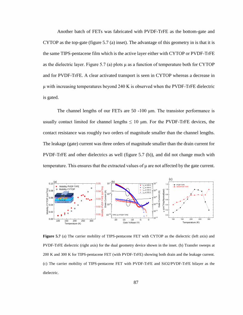
87
Another batch of FETs was fabricated with PVDF-TrFE as the bottom-gate and
CYTOP as the top-gate (figure 5.7 (a) inset). The advantage of this geometry in is that it is
the same TIPS-pentacene film which is the active layer either with CYTOP or PVDF-TrFE
as the dielectric layer. Figure 5.7 (a) plots μ as a function of temperature both for CYTOP
and for PVDF-TrFE. A clear activated transport is seen in CYTOP whereas a decrease in
μ with increasing temperatures beyond 240 K is observed when the PVDF-TrFE dielectric
is gated.
The channel lengths of our FETs are 50 -100 μm. The transistor performance is
usually contact limited for channel lengths ≤ 10 μm. For the PVDF-TrFE devices, the
contact resistance was roughly two orders of magnitude smaller than the channel lengths.
The leakage (gate) current was three orders of magnitude smaller than the drain current for
PVDF-TrFE and other dielectrics as well (figure 5.7 (b)), and did not change much with
temperature. This ensures that the extracted values of μ are not affected by the gate current.
Figure 5.7 (a) The carrier mobility of TIPS-pentacene FET with CYTOP as the dielectric (left axis) and
PVDF-TrFE dielectric (right axis) for the dual geometry device shown in the inset. (b) Transfer sweeps at
200 K and 300 K for TIPS-pentacene FET (with PVDF-TrFE) showing both drain and the leakage current.
(c) The carrier mobility of TIPS-pentacene FET with PVDF-TrFE and SiO2/PVDF-TrFE bilayer as the
dielectric.
100 150 200 250 3000.00
0.02
0.04
0.06
0.08
0.10
Mobility CYTOP
Mo
bili
ty C
YT
OP
(cm
2/V
s)
Temperature (K)
0.01
0.02
0.03
0.04
0.05
Mobility PVDF-TrFE
Mo
bili
ty P
VD
F-T
rFE
(cm
2/V
s)
-20 -15 -10 -5 0
10-10
10-9
10-8
10-7
IDS at 200 K
IDS at 300 K
IGS at 200 K
IGS at 300 K
Dra
in C
urr
en
t (A
)
Gate Voltage (V)
TIPS on PVDF-TrFE
10-12
10-11
10-10
10-9
10-8
10-7
Ga
te C
urr
en
t (A
)
(a) (b)
100 150 200 250 300
0.0
0.2
0.4
0.6
0.8
1.0
1.2 PVDF-TrFE
SiO2/PVDF-TrFE
(cm
2/V
s)(N
orm
aliz
ed
)
Temperature (K)
(c)
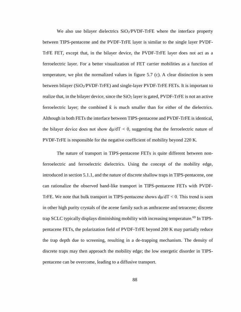
88
We also use bilayer dielectrics SiO2/PVDF-TrFE where the interface property
between TIPS-pentacene and the PVDF-TrFE layer is similar to the single layer PVDF-
TrFE FET, except that, in the bilayer device, the PVDF-TrFE layer does not act as a
ferroelectric layer. For a better visualization of FET carrier mobilities as a function of
temperature, we plot the normalized values in figure 5.7 (c). A clear distinction is seen
between bilayer (SiO2/PVDF-TrFE) and single-layer PVDF-TrFE FETs. It is important to
realize that, in the bilayer device, since the SiO2 layer is gated, PVDF-TrFE is not an active
ferroelectric layer; the combined ƙ is much smaller than for either of the dielectrics.
Although in both FETs the interface between TIPS-pentacene and PVDF-TrFE is identical,
the bilayer device does not show dμ/dT < 0, suggesting that the ferroelectric nature of
PVDF-TrFE is responsible for the negative coefficient of mobility beyond 220 K.
The nature of transport in TIPS-pentacene FETs is quite different between non-
ferroelectric and ferroelectric dielectrics. Using the concept of the mobility edge,
introduced in section 5.1.1, and the nature of discrete shallow traps in TIPS-pentacene, one
can rationalize the observed band-like transport in TIPS-pentacene FETs with PVDF-
TrFE. We note that bulk transport in TIPS-pentacene shows dμ/dT < 0. This trend is seen
in other high purity crystals of the acene family such as anthracene and tetracene; discrete
trap SCLC typically displays diminishing mobility with increasing temperature.69 In TIPS-
pentacene FETs, the polarization field of PVDF-TrFE beyond 200 K may partially reduce
the trap depth due to screening, resulting in a de-trapping mechanism. The density of
discrete traps may then approach the mobility edge; the low energetic disorder in TIPS-
pentacene can be overcome, leading to a diffusive transport.
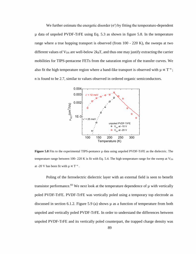
89
We further estimate the energetic disorder (σ′) by fitting the temperature-dependent
µ data of unpoled PVDF-TrFE using Eq. 5.3 as shown in figure 5.8. In the temperature
range where a true hopping transport is observed (from 100 - 220 K), the sweeps at two
different values of VDS are well-below 2kBT, and thus one may justify extracting the carrier
mobilities for TIPS-pentacene FETs from the saturation region of the transfer curves. We
also fit the high temperature region where a band-like transport is observed with µ ∝ T−n ;
n is found to be 2.7, similar to values observed in ordered organic semiconductors.
Figure 5.8 Fits to the experimental TIPS-pentance µ data using unpoled PVDF-TrFE as the dielectric. The
temperature range between 100- 220 K is fit with Eq. 5.4. The high temperature range for the sweep at VDS
at -20 V has been fit with µ ∝ T−n .
Poling of the ferroelectric dielectric layer with an external field is seen to benefit
transistor performance.83 We next look at the temperature dependence of µ with vertically
poled PVDF-TrFE. PVDF-TrFE was vertically poled using a temporary top electrode as
discussed in section 6.1.2. Figure 5.9 (a) shows µ as a function of temperature from both
unpoled and vertically poled PVDF-TrFE. In order to understand the differences between
unpoled PVDF-TrFE and its vertically poled counterpart, the trapped charge density was
100 150 200 250 300
1E-3
0.002
0.003
0.004
' = 12 meV
unpoled PVDF-TrFE
VDS
at -10 V
VDS
at -20 V
F
ET(c
m2/V
s)
Temperature (K)
' = 25 meV
90
estimated from the subthreshold swing of the FET characteristics. Figure 5.9 (b) plots
𝑁𝑡𝑟𝑎𝑝𝑚𝑎𝑥 for unpoled (swept at two different values of VDS) and poled PVDF-TrFE FETs.
Above 200 K, the trap density is seen to be an order of magnitude higher for the poled
dielectric film. The nature of transport with poled PVDF-TrFE is similar to other non-
ferroelectric dielectrics. These observations suggest that the energy fluctuations due to the
randomly oriented dipoles that are present locally in the unpoled PVDF-TrFE films, and
not the trapped charge density, are responsible for the band-like transport as well as lower
values of µ compared to poled PVDF-TrFE, seen above temperatures of 200 K. We want
to point out that the contact resistance of FETs used in this work are minimal as the channel
lengths are relatively large (50-100 µm). The contact resistance was at least two orders of
magnitude smaller than the channel resistance, and the difference between the poled and
unpoled FETs were minimal. Inset in figure 5.9 (b) shows the variation of threshold voltage
in unpoled and vertically poled PVDF-TrFE FETs.
Figure 5.9 (a) TIPS-pentacene FET mobility as a function of temperature at two different VDS values for
unpoled PVDF-TrFE. The blue triangles are the FET mobility from a TIPS-pentacene FET where the PVDF-
100 150 200 250 300 350
10-4
10-3
VDS
at -10 V
VDS
at -20 V
F
ET(c
m2/V
s)
Temperature (K)
10-4
10-3
10-2
10-1
F
ET (
cm
2/V
s)
100 150 200 250 300 3500
2x10¹²
4x10¹²
6x10¹²
8x10¹²
1x10¹³
100 150 200 250 300-10
-9
-8
-7
-6
-5
-4
VT
H (
V)
Temperature (K)
unpoled (VDS=-10 V)
unpoled (VDS=-20 V)
poled
Ntr
ap M
ax (
cm
-2)
Temperature (K)
PVDF-TrFE
(a) (b)
V-poled
91
TrFE dielectric layer was vertically poled. (b)The trapped charge density as a function of temperature for
TIPS-pentacene FETs using unpoled and vertically poled PVDF-TrFE.
In conclusion, polarization fluctuation inherent to PVDF-TrFE influences transport
in other organic FETs as well. Drop-casted TIPS-pentacene films exhibit single-trap-level
SCLC, similar to high-purity crystalline organic molecules. A bulk-transport measurement
from TIPS-pentacene clearly shows a negative coefficient of mobility beyond 180 K. A
similar behavior is seen in FET transport when a ferroelectric dielectric, PVDF-TrFE, is
used. The presence of a polarization field of the ferroelectric dielectric results in a transport
mechanism, exemplifying a band-like transport above a certain temperature. By fitting the
high temperature regime of unpoled PVDF-TrFE devices to μ=T-n, n was found to be 2.7,
similar to values obtained for ordered organic semiconductors. All other non-ferroelectric
dielectrics and poled PVDF-TrFE (where the dipoles are prealigned) show an activated
transport similar to Al2O3, suggesting that the reduced mobility with unpoled PVDF-TrFE
is not just due to the long-range polaron coupling but rather due to its inherent polarization
fluctuation in conjunction with the nature of discrete trap-states in TIPS-pentacene.
92
6 Dipole engineering of ferroelectric dielectrics- enhancement
in FET performance
In chapters 4 and 5 we gave several examples to show the influence of PVDF-TrFE
in organic FETs. This helps us to understand the charge transport mechanism in such
devices. The formation of Fröhlich polarons suppresses the FET mobility, reducing the
performance of such FETs. PVDF-TrFE, in spite of its applications in vast range of work
including as a gate dielectric in organic FETs48, 60, 84, 85 and sensing applications86, 87, pose
some concerns. These concerns are related to its inherent surface roughness issues as well
as higher conductivity compared to other polymer non-ferroelectric dielectrics; the DC
conductivity of PVDF (of approximately 10-12 S/m) is a few orders higher than other
polymer dielectrics such as poly-methylmethacrylate (PMMA).88 Additionally, the dipolar
disorder at the semiconductor-PVDF-TrFE interface in FET architectures is higher
compared to other polymer ferroelectrics. As a result PVDF-TrFE as a dielectric layer in
organic FETs show low carrier mobilities in comparison to non-ferroelectric polymer
dielectrics.85 To use PVDF-TrFE as a gate dielectric, we thus need to enhance the FET
performance. In this chapter we will discuss the techniques developed by us to enhance the
performance of organic FETs performance based on PVDF-TrFE. We use the method of
dipole engineering of the PVDF-TrFE film. In particular we have come up with new
methods of electrical poling the dielectric layer to enhance FET performance as well as
reduce gate leakage issues. This chapter includes two parts: (a) polarization rotation in the
dielectric PVDF-TrFE and (b) textured poling of dielectric PVDF-TrFE.
93
6.1 Polarization rotation in the dielectric PVDF-TrFE
6.1.1 Introduction
A juxtaposition of ferroelectric polymers and ferroelectric oxides shows MOSFETs
have greatly benefited from the intrinsic spontaneous electric polarization of ferroelectric
oxides. Polarization modulation in ferroelectric oxides has enabled fast switching and low-
power operation in MOSFETs.89, 90 The spontaneous electric polarization of ferroelectric
oxides not only controls the channel conductance but may be further reoriented by the
application of an external electric field.91, 92 Although the polarization distribution effect of
the ferroelectric oxide on the channel current-gate voltage has been considered in
MOSFETs.93, 94 There are no such parallel studies on polymer ferroelectric FETs,
especially where the effect of rotating the polarization direction by 90o on FET
performance has been examined.
Theoretical work shows the effect of polarization rotation on the performance of
MOSFETs using BaTiO3 as the gate insulator.35 Polarization rotation changes the surface
potential of the silicon substrate, resulting in a subthreshold swing (SS) lower than 60
mV/decade by a judicious choice of the thickness of the gate dielectric layer. It is seen that
polarization rotation (from out-of-plane to in-plane) offers significant advantages over
polarization inversion in the BaTiO3 layer. Spontaneous polarization during the
reorientation increases the screening charge accumulation in the MOSFET channel,
resulting in low SS. Although the SS of FETs based on polycrystalline organic films have
now paralleled those of MOSFETs with values close to 90 mV/decade,36, 37 they usually
involve a self-assembled monolayer on high-quality oxide dielectrics such as AlOx. In
94
single crystal rubrene FETs, the disorder is significantly reduced with interface trap
densities similar to that in silicon transistors, and SS values of 65 mV/decade have been
achieved.38 A question that arises is whether polarization reorientation in a polymer
ferroelectric dielectric is an effective mechanism for improving SS and other transistor
parameters in organic FETs. Specifically, we are interested in changes in SS and other FET
parameters by rotating the polarization direction of the dielectric by 90o. Polarization
rotation is different from polarization inversion, which in principle may be achieved by
sweeping the gate from high negative to positive voltages in ferroelectric organic FETs.
Such inversion effects have benefits in changing the on/off ratio for memory application.
By using two different organic molecules: DNTT and pentacene, and solution
processable semiconductor TIPS-pentacene along with unpoled and poled PVDF-TrFE as
the gate dielectric, in top-contact bottom-gate FET architectures, carrier transport is
investigated. Prior to depositing the organic semiconductor, the ferroelectric film is either
vertically or laterally poled by applying an external electric field while heating the polymer
just above its ferroelectric-paraelectric transition temperature at 135oC, which is known to
increase the degree of crystallinity.95 The presence of additional lateral electrodes with
vertically poled FETs facilitates the application of a lateral electric field, which helps to
monitor transistor properties as a function of reorientation of the polarization direction by
90o in the dielectric medium. Since we investigate p-type transport, the poling direction is
appropriately chosen so that the operating field does not work against the poling field. The
FETs with vertically poled PVDF-TrFE film perform the best with the lowest value of SS.
As a lateral electric field on the top surface is applied to the vertically poled FETs, the
transistor characteristics are seen to degrade. The phenomenon is reversible; by applying a
95
lateral field in the opposite direction, the transistor properties recover. The FETs operate
at lower voltages compared to the coercive voltage of the PVDF-TrFE layer, ensuring that
the changes observed in the FET properties arise from external poling conditions. The
poling field controls the microstructure of PVDF-TrFE, which is inferred from x-ray
diffraction (XRD) and electron microscopy images. Density-functional-theory (DFT)
studies from a monomer unit embedded in a dielectric medium under the application of
both vertical and horizontal electric fields shed light on the changes in the net dipole
moment and structure (deviation from the all-trans phase) of the molecule. This study
highlights new design principles for organic FETs in lowering SS and enhancing transport
properties by orienting the polarization direction by 90o in the ferroelectric dielectric layer.
6.1.2 Poling of PVDF-TrFE films
PVDF-TrFE is dissolved in the solvent N, N-dimethylformamide (50 mg/ml)
(DMF). This dielectric solution is then spin casted on top of the Al-coated glass at a spin
speed of 1600 rpm for 60 sec and heated at 70oC for 10 minutes to remove the solvent
residue. The PVDF-TrFE films are then annealed at 135oC for half an hour for further
enhancement of the β phase of the copolymer. A temporary electrode is prepared by
depositing 300 nm of Al on a glass slide. Electrical contacts are made, and the slide is
placed (with the Al strip facing down) on top of the PVDF-TrFE film, as shown in figure
6.1(a). A 50-g weight is added on top to ensure a uniform contact of the top electrode with
the ferroelectric surface. PVDF-TrFE films are vertically poled by applying an electric
field of ∼100 MV/m during the crystallization process. The field is on while the film is
allowed to slow cool for half an hour. Two aluminum strips, 2.0 mm apart, are deposited
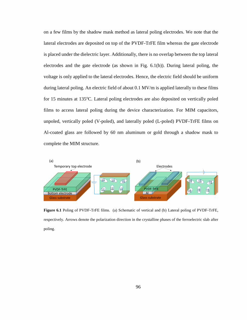
96
on a few films by the shadow mask method as lateral poling electrodes. We note that the
lateral electrodes are deposited on top of the PVDF-TrFE film whereas the gate electrode
is placed under the dielectric layer. Additionally, there is no overlap between the top lateral
electrodes and the gate electrode (as shown in Fig. 6.1(b)). During lateral poling, the
voltage is only applied to the lateral electrodes. Hence, the electric field should be uniform
during lateral poling. An electric field of about 0.1 MV/m is applied laterally to these films
for 15 minutes at 135oC. Lateral poling electrodes are also deposited on vertically poled
films to access lateral poling during the device characterization. For MIM capacitors,
unpoled, vertically poled (V-poled), and laterally poled (L-poled) PVDF-TrFE films on
Al-coated glass are followed by 60 nm aluminum or gold through a shadow mask to
complete the MIM structure.
Figure 6.1 Poling of PVDF-TrFE films. (a) Schematic of vertical and (b) Lateral poling of PVDF-TrFE,
respectively. Arrows denote the polarization direction in the crystalline phases of the ferroelectric slab after
poling.
Glass substrate
PVDF-TrFE
Electrodes
Glass substrate
Bottom electrodePVDF-TrFE
Temporary top electrode
(a) (b)
Al
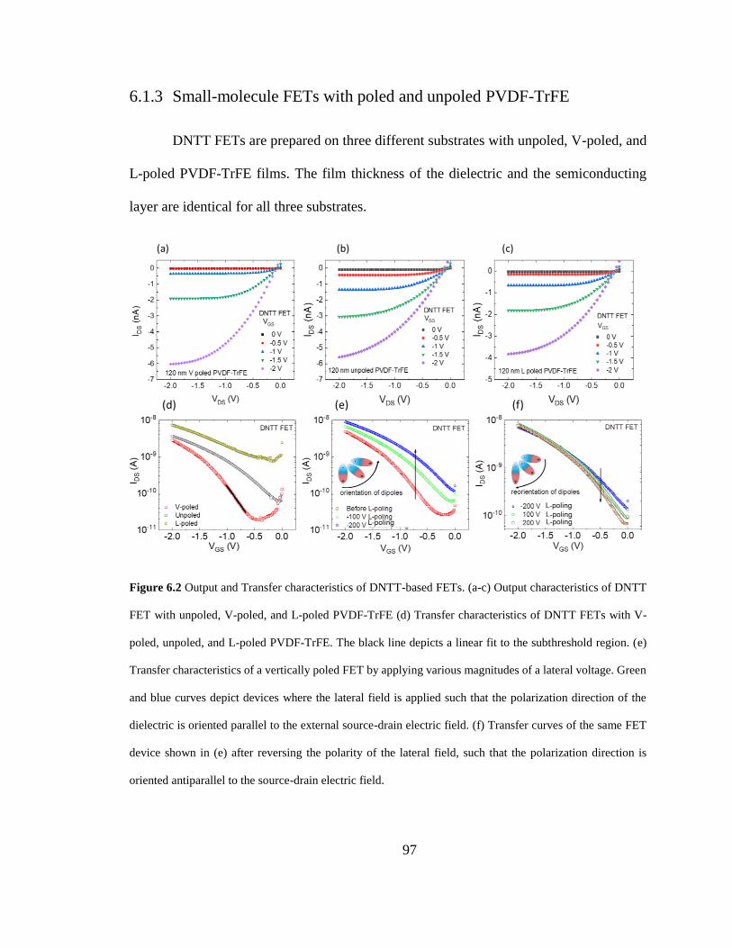
97
6.1.3 Small-molecule FETs with poled and unpoled PVDF-TrFE
DNTT FETs are prepared on three different substrates with unpoled, V-poled, and
L-poled PVDF-TrFE films. The film thickness of the dielectric and the semiconducting
layer are identical for all three substrates.
Figure 6.2 Output and Transfer characteristics of DNTT-based FETs. (a-c) Output characteristics of DNTT
FET with unpoled, V-poled, and L-poled PVDF-TrFE (d) Transfer characteristics of DNTT FETs with V-
poled, unpoled, and L-poled PVDF-TrFE. The black line depicts a linear fit to the subthreshold region. (e)
Transfer characteristics of a vertically poled FET by applying various magnitudes of a lateral voltage. Green
and blue curves depict devices where the lateral field is applied such that the polarization direction of the
dielectric is oriented parallel to the external source-drain electric field. (f) Transfer curves of the same FET
device shown in (e) after reversing the polarity of the lateral field, such that the polarization direction is
oriented antiparallel to the source-drain electric field.
98
Figure 6.2 (a-c) show the output characteristics of DNTT FET with unpoled, V-
poled, and L-poled PVDF-TrFE. The device size was identical for all of them (W=1mm
and L= 100 µm). Corresponding transfer characteristics of these DNTT FETs with V-
poled, unpoled, and L-poled PVDF-TrFE are shown in figure 6.2 (d). These are all swept
in the saturation region where the drain-source voltage (VDS) is maintained at −2 V, and
the gate voltage (VGS) is varied. Device parameters such as carrier mobility, on-off current
ratio, and threshold (VTh) are estimated using the standard saturation regime current-
voltage characteristics. Channel length varied between 50 and 125 μm for the FETs. More
than the changes in μ, the subthreshold swing and other FET parameters, as discussed
below, vary with the poling condition; hence, we quote only the saturation mobilities. Work
by Choi et al. defines the reliability factor r for extracting carrier mobilities both in the
saturation and linear regions of the transfer characteristics. The r factor is defined based on
the ideal Shockley FET equations with VTh = 0 and can be expressed as 96,
𝑟 = {√𝐼𝐷𝑆
𝑀𝑎𝑥−√𝐼𝐷𝑆𝑜
𝑉𝐺𝑆𝑀𝑎𝑥
}
2
/(𝜕√𝐼𝐷𝑆
𝜕𝑉𝐺𝑆)2 (6.1)
Based on this definition, the r factor for μsat (V-poled FET) is found to be ∼47%.
We point out that for ferroelectric dielectrics the value of VTh can greatly vary, from being
positive to negative, as discussed later. Hence, one cannot expect an ideal r factor of
∼100%.
The SS varies for the unpoled, V-poled, and L-poled PVDF-TrFE FETs. A
representative linear fit (black line) for the V-poled device is shown in figure 6.2(d). We
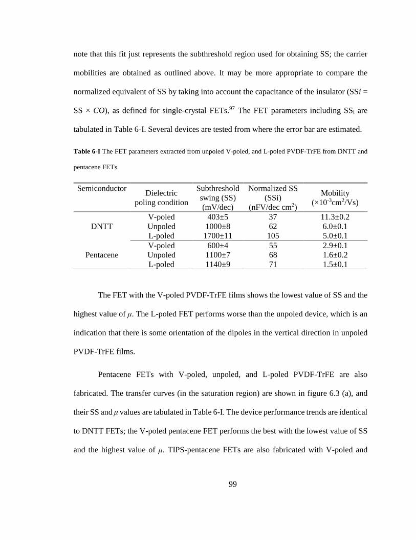
99
note that this fit just represents the subthreshold region used for obtaining SS; the carrier
mobilities are obtained as outlined above. It may be more appropriate to compare the
normalized equivalent of SS by taking into account the capacitance of the insulator (SSi =
SS × CO), as defined for single-crystal FETs.97 The FET parameters including SSi are
tabulated in Table 6-I. Several devices are tested from where the error bar are estimated.
Table 6-I The FET parameters extracted from unpoled V-poled, and L-poled PVDF-TrFE from DNTT and
pentacene FETs.
Semiconductor Dielectric
poling condition
Subthreshold
swing (SS)
(mV/dec)
Normalized SS
(SSi)
(nFV/dec cm2)
Mobility
(×10-3cm2/Vs)
DNTT
V-poled 403±5 37 11.3±0.2
Unpoled 1000±8 62 6.0±0.1
L-poled 1700±11 105 5.0±0.1
Pentacene
V-poled 600±4 55 2.9±0.1
Unpoled 1100±7 68 1.6±0.2
L-poled 1140±9 71 1.5±0.1
The FET with the V-poled PVDF-TrFE films shows the lowest value of SS and the
highest value of μ. The L-poled FET performs worse than the unpoled device, which is an
indication that there is some orientation of the dipoles in the vertical direction in unpoled
PVDF-TrFE films.
Pentacene FETs with V-poled, unpoled, and L-poled PVDF-TrFE are also
fabricated. The transfer curves (in the saturation region) are shown in figure 6.3 (a), and
their SS and μ values are tabulated in Table 6-I. The device performance trends are identical
to DNTT FETs; the V-poled pentacene FET performs the best with the lowest value of SS
and the highest value of μ. TIPS-pentacene FETs are also fabricated with V-poled and
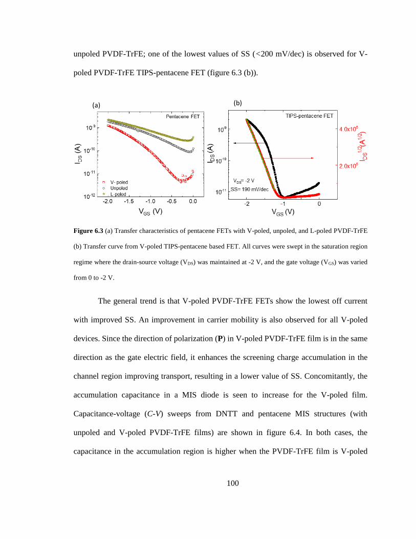
100
unpoled PVDF-TrFE; one of the lowest values of SS (<200 mV/dec) is observed for V-
poled PVDF-TrFE TIPS-pentacene FET (figure 6.3 (b)).
Figure 6.3 (a) Transfer characteristics of pentacene FETs with V-poled, unpoled, and L-poled PVDF-TrFE
(b) Transfer curve from V-poled TIPS-pentacene based FET. All curves were swept in the saturation region
regime where the drain-source voltage (VDS) was maintained at -2 V, and the gate voltage (VGS) was varied
from 0 to -2 V.
The general trend is that V-poled PVDF-TrFE FETs show the lowest off current
with improved SS. An improvement in carrier mobility is also observed for all V-poled
devices. Since the direction of polarization (P) in V-poled PVDF-TrFE film is in the same
direction as the gate electric field, it enhances the screening charge accumulation in the
channel region improving transport, resulting in a lower value of SS. Concomitantly, the
accumulation capacitance in a MIS diode is seen to increase for the V-poled film.
Capacitance-voltage (C-V) sweeps from DNTT and pentacene MIS structures (with
unpoled and V-poled PVDF-TrFE films) are shown in figure 6.4. In both cases, the
capacitance in the accumulation region is higher when the PVDF-TrFE film is V-poled
(a) (b)
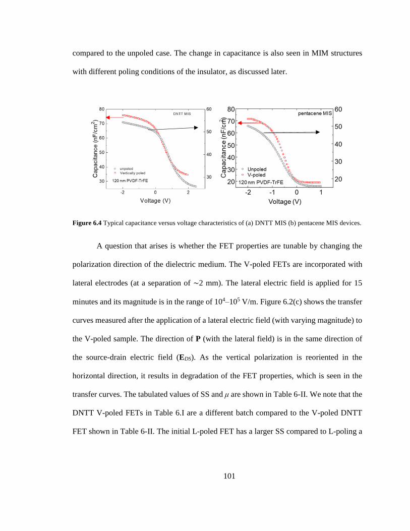
101
compared to the unpoled case. The change in capacitance is also seen in MIM structures
with different poling conditions of the insulator, as discussed later.
Figure 6.4 Typical capacitance versus voltage characteristics of (a) DNTT MIS (b) pentacene MIS devices.
A question that arises is whether the FET properties are tunable by changing the
polarization direction of the dielectric medium. The V-poled FETs are incorporated with
lateral electrodes (at a separation of ∼2 mm). The lateral electric field is applied for 15
minutes and its magnitude is in the range of 104–105 V/m. Figure 6.2(c) shows the transfer
curves measured after the application of a lateral electric field (with varying magnitude) to
the V-poled sample. The direction of P (with the lateral field) is in the same direction of
the source-drain electric field (EDS). As the vertical polarization is reoriented in the
horizontal direction, it results in degradation of the FET properties, which is seen in the
transfer curves. The tabulated values of SS and μ are shown in Table 6-II. We note that the
DNTT V-poled FETs in Table 6.I are a different batch compared to the V-poled DNTT
FET shown in Table 6-II. The initial L-poled FET has a larger SS compared to L-poling a
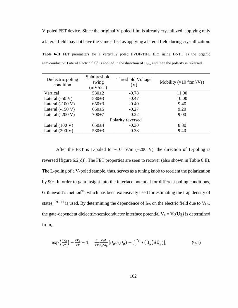
102
V-poled FET device. Since the original V-poled film is already crystallized, applying only
a lateral field may not have the same effect as applying a lateral field during crystallization.
Table 6-II FET parameters for a vertically poled PVDF-TrFE film using DNTT as the organic
semiconductor. Lateral electric field is applied in the direction of EDS, and then the polarity is reversed.
Dielectric poling
condition
Subthreshold
swing
(mV/dec)
Threshold Voltage
(V) Mobility (×10-3cm2/Vs)
Vertical 530±2 -0.78 11.00
Lateral (-50 V) 580±3 -0.47 10.00
Lateral (-100 V) 650±3 -0.40 9.40
Lateral (-150 V) 660±5 -0.27 9.20
Lateral (-200 V) 700±7 -0.22 9.00
Polarity reversed
Lateral (100 V) 650±4 -0.30 8.30
Lateral (200 V) 580±3 -0.33 9.40
After the FET is L-poled to ∼105 V/m (−200 V), the direction of L-poling is
reversed [figure 6.2(d)]. The FET properties are seen to recover (also shown in Table 6.II).
The L-poling of a V-poled sample, thus, serves as a tuning knob to reorient the polarization
by 90o. In order to gain insight into the interface potential for different poling conditions,
Grünewald’s method98, which has been extensively used for estimating the trap density of
states, 99, 100 is used. By determining the dependence of IDS on the electric field due to VGS,
the gate-dependent dielectric-semiconductor interface potential Vo = V0(Ug) is determined
from,
exp (𝑒𝑉𝑜
𝑘𝑇) −
𝑒𝑉𝑜
𝑘𝑇− 1 =
𝑒
𝑘𝑇
𝜖𝑖𝑑
𝜖𝑠𝑙𝜎0[𝑈𝑔𝜎(𝑈𝑔) − ∫ 𝜎
𝑈𝑔
0(Ũ𝑔)𝑑Ũ𝑔)], (6.1)
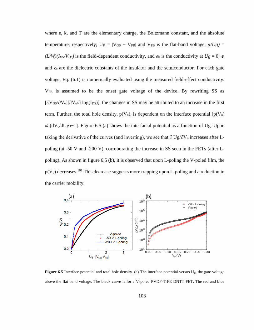
103
where e, k, and T are the elementary charge, the Boltzmann constant, and the absolute
temperature, respectively; Ug = |VGS − VFB| and VFB is the flat-band voltage; σ(Ug) =
(L/W)(IDS/VDS) is the field-dependent conductivity, and σ0 is the conductivity at Ug = 0; 𝛜i
and 𝛜s are the dielectric constants of the insulator and the semiconductor. For each gate
voltage, Eq. (6.1) is numerically evaluated using the measured field-effect conductivity.
VFB is assumed to be the onset gate voltage of the device. By rewriting SS as
[∂VGS/∂Vo][∂Vo/∂ log(IDS)], the changes in SS may be attributed to an increase in the first
term. Further, the total hole density, p(Vo), is dependent on the interface potential [p(Vo)
∝ (dVo/dUg)−1]. Figure 6.5 (a) shows the interfacial potential as a function of Ug. Upon
taking the derivative of the curves (and inverting), we see that ∂ Ug/∂Vo increases after L-
poling (at -50 V and -200 V), corroborating the increase in SS seen in the FETs (after L-
poling). As shown in figure 6.5 (b), it is observed that upon L-poling the V-poled film, the
p(Vo) decreases.101 This decrease suggests more trapping upon L-poling and a reduction in
the carrier mobility.
Figure 6.5 Interface potential and total hole density. (a) The interface potential versus Ug, the gate voltage
above the flat band voltage. The black curve is for a V-poled PVDF-TrFE DNTT FET. The red and blue
0.00 0.05 0.10 0.15 0.20 0.25 0.301020
1021
1022
1023
1024
1025
-50 V L-poling
V poled
p(V
0)
(m-3
)
Vo (V)
A B(a) (b)
Ug
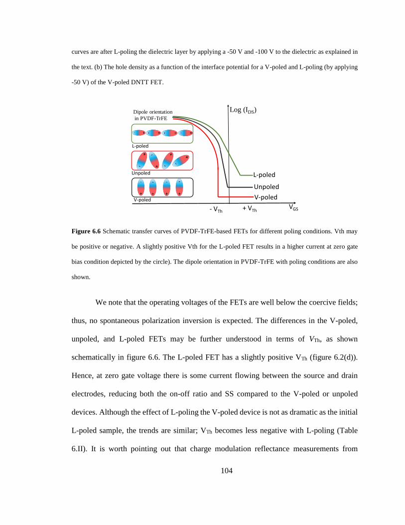
104
curves are after L-poling the dielectric layer by applying a -50 V and -100 V to the dielectric as explained in
the text. (b) The hole density as a function of the interface potential for a V-poled and L-poling (by applying
-50 V) of the V-poled DNTT FET.
Figure 6.6 Schematic transfer curves of PVDF-TrFE-based FETs for different poling conditions. Vth may
be positive or negative. A slightly positive Vth for the L-poled FET results in a higher current at zero gate
bias condition depicted by the circle). The dipole orientation in PVDF-TrFE with poling conditions are also
shown.
We note that the operating voltages of the FETs are well below the coercive fields;
thus, no spontaneous polarization inversion is expected. The differences in the V-poled,
unpoled, and L-poled FETs may be further understood in terms of VTh, as shown
schematically in figure 6.6. The L-poled FET has a slightly positive VTh (figure 6.2(d)).
Hence, at zero gate voltage there is some current flowing between the source and drain
electrodes, reducing both the on-off ratio and SS compared to the V-poled or unpoled
devices. Although the effect of L-poling the V-poled device is not as dramatic as the initial
L-poled sample, the trends are similar; VTh becomes less negative with L-poling (Table
6.II). It is worth pointing out that charge modulation reflectance measurements from
VGS
Log (IDS)
L-poled
Unpoled
V-poledV-poled
Unpoled
L-poled
Dipole orientation
in PVDF-TrFE
+ VTh- VTh
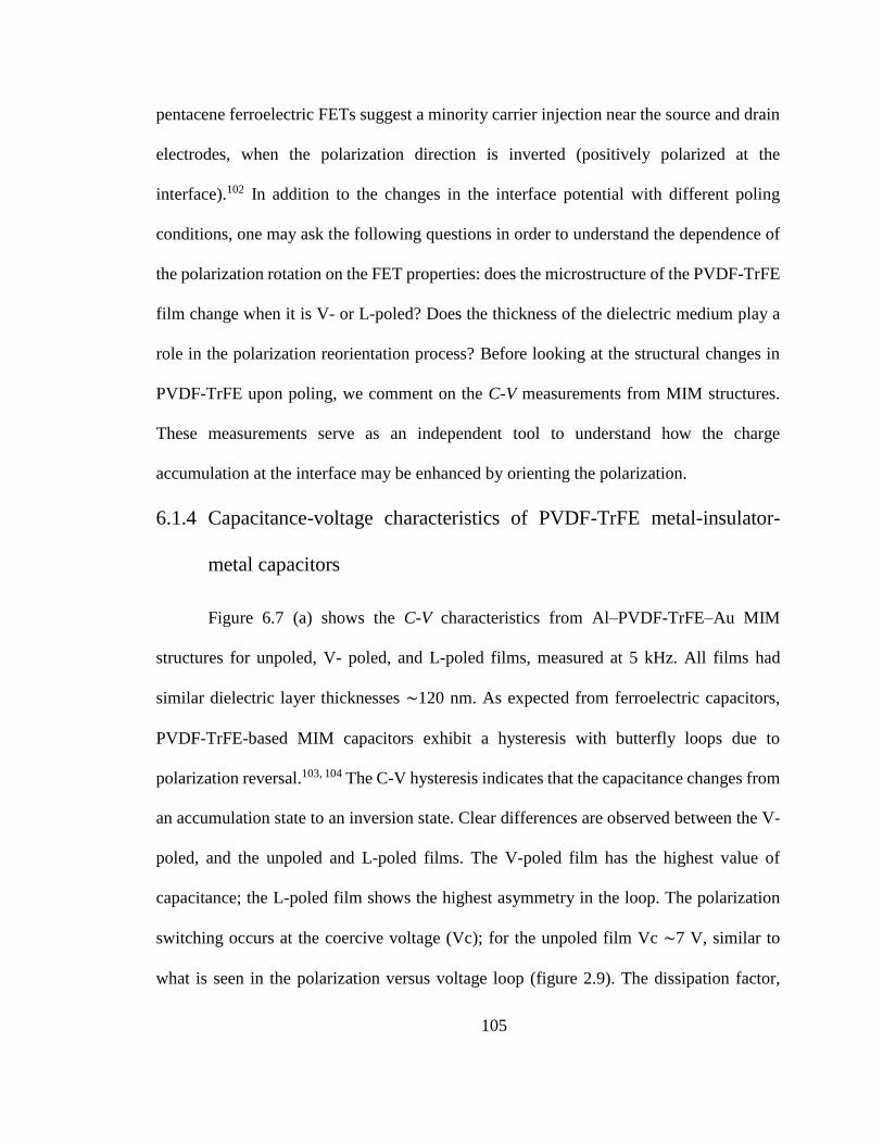
105
pentacene ferroelectric FETs suggest a minority carrier injection near the source and drain
electrodes, when the polarization direction is inverted (positively polarized at the
interface).102 In addition to the changes in the interface potential with different poling
conditions, one may ask the following questions in order to understand the dependence of
the polarization rotation on the FET properties: does the microstructure of the PVDF-TrFE
film change when it is V- or L-poled? Does the thickness of the dielectric medium play a
role in the polarization reorientation process? Before looking at the structural changes in
PVDF-TrFE upon poling, we comment on the C-V measurements from MIM structures.
These measurements serve as an independent tool to understand how the charge
accumulation at the interface may be enhanced by orienting the polarization.
6.1.4 Capacitance-voltage characteristics of PVDF-TrFE metal-insulator-
metal capacitors
Figure 6.7 (a) shows the C-V characteristics from Al–PVDF-TrFE–Au MIM
structures for unpoled, V- poled, and L-poled films, measured at 5 kHz. All films had
similar dielectric layer thicknesses ∼120 nm. As expected from ferroelectric capacitors,
PVDF-TrFE-based MIM capacitors exhibit a hysteresis with butterfly loops due to
polarization reversal.103, 104 The C-V hysteresis indicates that the capacitance changes from
an accumulation state to an inversion state. Clear differences are observed between the V-
poled, and the unpoled and L-poled films. The V-poled film has the highest value of
capacitance; the L-poled film shows the highest asymmetry in the loop. The polarization
switching occurs at the coercive voltage (Vc); for the unpoled film Vc ∼7 V, similar to
what is seen in the polarization versus voltage loop (figure 2.9). The dissipation factor,
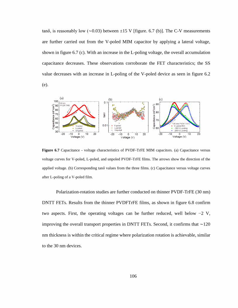
106
tanδ, is reasonably low (∼0.03) between ±15 V [figure. 6.7 (b)]. The C-V measurements
are further carried out from the V-poled MIM capacitor by applying a lateral voltage,
shown in figure 6.7 (c). With an increase in the L-poling voltage, the overall accumulation
capacitance decreases. These observations corroborate the FET characteristics; the SS
value decreases with an increase in L-poling of the V-poled device as seen in figure 6.2
(e).
Figure 6.7 Capacitance - voltage characteristics of PVDF-TrFE MIM capacitors. (a) Capacitance versus
voltage curves for V-poled, L-poled, and unpoled PVDF-TrFE films. The arrows show the direction of the
applied voltage. (b) Corresponding tanδ values from the three films. (c) Capacitance versus voltage curves
after L-poling of a V-poled film.
Polarization-rotation studies are further conducted on thinner PVDF-TrFE (30 nm)
DNTT FETs. Results from the thinner PVDFTrFE films, as shown in figure 6.8 confirm
two aspects. First, the operating voltages can be further reduced, well below −2 V,
improving the overall transport properties in DNTT FETs. Second, it confirms that ∼120
nm thickness is within the critical regime where polarization rotation is achievable, similar
to the 30 nm devices.
107
Figure 6.8 Typical FET characteristics of DNTT based devices with 30 nm PVDF-TrFE layer. (a) The
voltage between source and drain was swept from 0 to -1.6 V to obtain the output characteristics at various
gate voltages varying from 0 to -1.6 V. (b) The transfer curve was swept in the saturation region where the
drain-source voltage (VDS) was maintained at -1.6 V, and the gate voltage (VGS) was varied from 0 to -1.6 V.
Both output and transfer curves were from a V-poled PVDF-TrFE based FET. (c) Transfer characteristics of
a V-poled FET after applying two different lateral electric fields. The lateral field was applied such that the
polarization direction of the dielectric is oriented parallel to the external source-drain electric field.
Irrespective of the organic semiconductor layer, our results show that the
polarization orientation in the polymer ferroelectric layer directly impacts FET
performance. In particular, SS of the FET transfer characteristics may be lowered by
orienting P in a direction parallel to the applied gate electric field. This agrees well with
some of the highest switching times that have been observed for polymer ferroelectric FETs
when the interface layer is pre-biased in the perpendicular direction.83 In order to
understand how the microstructure affects the overall polarization in the ferroelectric layer,
we obtain SEM images and conduct XRD studies from poled and unpoled PVDF-TrFE
films. To obtain a better signal-to-noise ratio, the sample thickness for the XRD
measurements is higher than what is used in FETs. The PVDF-TrFE films are deposited
on Si++ with thickness ∼800 nm.
(a) (b) (c)
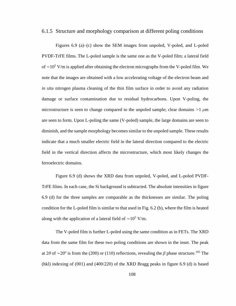
108
6.1.5 Structure and morphology comparison at different poling conditions
Figures 6.9 (a)–(c) show the SEM images from unpoled, V-poled, and L-poled
PVDF-TrFE films. The L-poled sample is the same one as the V-poled film; a lateral field
of ∼105 V/m is applied after obtaining the electron micrographs from the V-poled film. We
note that the images are obtained with a low accelerating voltage of the electron beam and
in situ nitrogen plasma cleaning of the thin film surface in order to avoid any radiation
damage or surface contamination due to residual hydrocarbons. Upon V-poling, the
microstructure is seen to change compared to the unpoled sample; clear domains >1 μm
are seen to form. Upon L-poling the same (V-poled) sample, the large domains are seen to
diminish, and the sample morphology becomes similar to the unpoled sample. These results
indicate that a much smaller electric field in the lateral direction compared to the electric
field in the vertical direction affects the microstructure, which most likely changes the
ferroelectric domains.
Figure 6.9 (d) shows the XRD data from unpoled, V-poled, and L-poled PVDF-
TrFE films. In each case, the Si background is subtracted. The absolute intensities in figure
6.9 (d) for the three samples are comparable as the thicknesses are similar. The poling
condition for the L-poled film is similar to that used in Fig. 6.2 (b), where the film is heated
along with the application of a lateral field of ∼105 V/m.
The V-poled film is further L-poled using the same condition as in FETs. The XRD
data from the same film for these two poling conditions are shown in the inset. The peak
at 2θ of ∼20o is from the (200) or (110) reflections, revealing the β phase structure.105 The
(hkl) indexing of (001) and (400/220) of the XRD Bragg peaks in figure 6.9 (d) is based
109
on the pseudohexagonal nature of the ferroelectric (FE) phase.106 The V-poled sample
shows the strongest intensity for the (200) or (110) reflection, suggesting an enhancement
of the overall β phase. The L-poled and unpoled samples are almost identical except for a
shoulder peak at ∼19o, which is more pronounced for the L-poled sample. This shoulder is
most likely a signature of the α and γ phases of the paraelectric (PE) phase107; the
deconvolution of the spectrum as two Gaussian peaks is shown in figure 6.9 (e).
The enhanced intensity of the β phase diffraction in PVDF-TrFE upon V-poling
may be understood from previous XRD measurements in PVDF. The increase in
polarization of a PVDF film (upon poling) originates from reorientation of the dipoles in
the crystalline phase by an electric field rather than orientation of the dipoles of the
amorphous (PE) phase.108-110 It is pointed out that although the β phase unit cell is
orthorhombic, it is very close to being hexagonal.111 A small distortion of the primitive
hexagonal unit cell is required to yield the β phase unit cell. A slight change in the peak
position of the (200) or (110) reflection (of the β phase) upon V-poling compared to the
unpoled sample in figure 6.9 (d) may reflect a unit cell closer to the β phase unit cell. Due
to the overlapping reflections, it is difficult to predict the exact lattice constants from our
experiments.
110
Figure 6.9 Structure and morphology of PVDF-TrFE as a function of poling. (a)–(c) Scanning electron
micrographs from unpoled, V-poled, and laterally L-poled films. (d) Grazing-incidence XRD from unpoled,
V-poled, and Lpoled PVDF-TrFE films on Si substrate. The (hkl) indexing is based on the ferroelectric phase
as discussed in the text. (e) The XRD from the V-poled film and after L-poling the same V-poled film.
Deconvolution of two peaks at 2θ (deg) (β phase) and at 18o for the paraelectric phase (PE) are shown for the
laterally poled film.
Since the sample thickness of PVDF-TrFE for XRD measurements is about eight
times more than those used in FETs, the polarization changes for the L-poled sample may
even be higher in the FET devices compared to what is observed in Fig. 6.9(d). A small
change in the XRD intensity after L-poling the V-poled film (in the inset) reflects a
reorientation of the dipole moment of the unit cell that affects the β phase. However, this
change is much smaller compared to the L-poled film, which is poled during
unpoled V-poled L-poled
(a) (b) (c)
(d) (e)
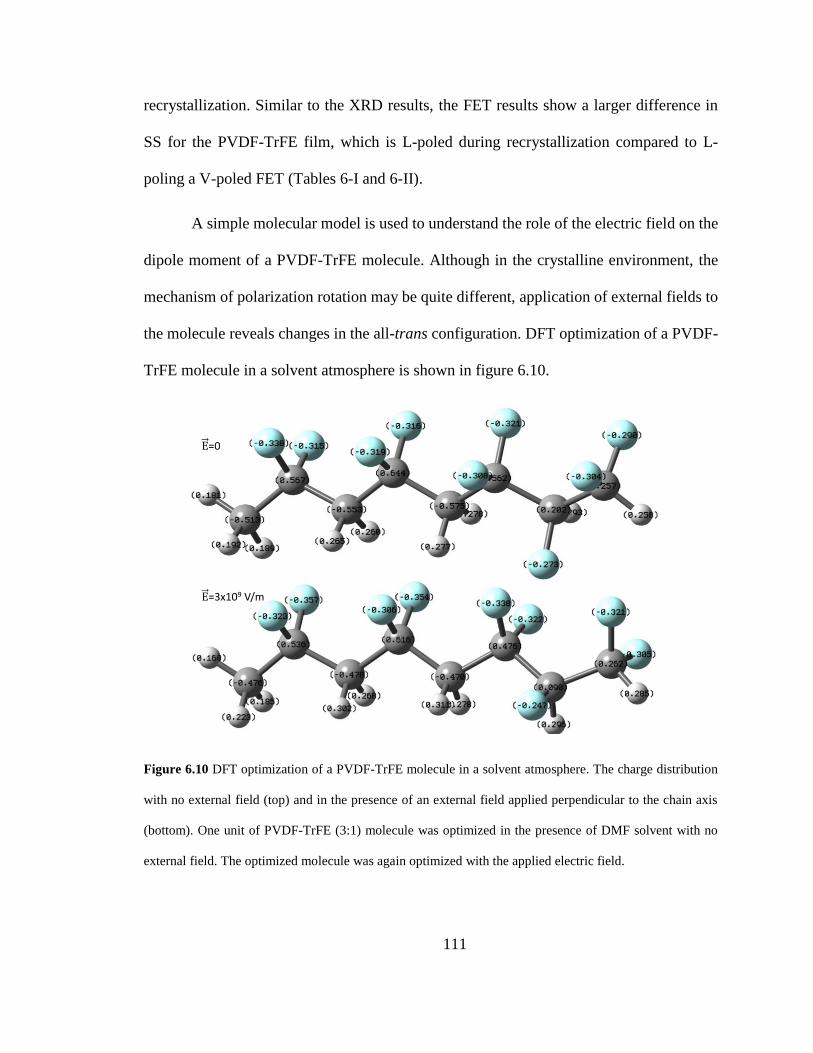
111
recrystallization. Similar to the XRD results, the FET results show a larger difference in
SS for the PVDF-TrFE film, which is L-poled during recrystallization compared to L-
poling a V-poled FET (Tables 6-I and 6-II).
A simple molecular model is used to understand the role of the electric field on the
dipole moment of a PVDF-TrFE molecule. Although in the crystalline environment, the
mechanism of polarization rotation may be quite different, application of external fields to
the molecule reveals changes in the all-trans configuration. DFT optimization of a PVDF-
TrFE molecule in a solvent atmosphere is shown in figure 6.10.
Figure 6.10 DFT optimization of a PVDF-TrFE molecule in a solvent atmosphere. The charge distribution
with no external field (top) and in the presence of an external field applied perpendicular to the chain axis
(bottom). One unit of PVDF-TrFE (3:1) molecule was optimized in the presence of DMF solvent with no
external field. The optimized molecule was again optimized with the applied electric field.
=0
=3x10⁹ V/m
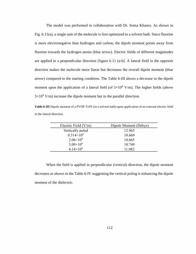
112
The model was performed in collaboration with Dr. Soma Khanra. As shown in
Fig. 6.11(a), a single unit of the molecule is first optimized in a solvent bath. Since fluorine
is more electronegative than hydrogen and carbon, the dipole moment points away from
fluorine towards the hydrogen atoms (blue arrow). Electric fields of different magnitudes
are applied in a perpendicular direction [figure 6.11 (a-b]. A lateral field in the opposite
direction makes the molecule more linear but decreases the overall dipole moment (blue
arrow) compared to the starting condition. The Table 6-III shows a decrease in the dipole
moment upon the application of a lateral field (of 5×10⁸ V/m). The higher fields (above
5×10⁹ V/m) increase the dipole moment but in the parallel direction.
Table 6-III Dipole moment of a PVDF-TrFE (in a solvent bath) upon application of an external electric field
in the lateral direction.
Electric Field (V/m) Dipole Moment (Debye)
Vertically poled 12.963
0.514×10⁹ 10.669
2.06×10⁹ 10.665
3.09×10⁹ 10.749
4.14×10⁹ 11.082
When the field is applied in perpendicular (vertical) direction, the dipole moment
decreases as shown in the Table 6-IV suggesting the vertical poling is enhancing the dipole
moment of the dielectric.
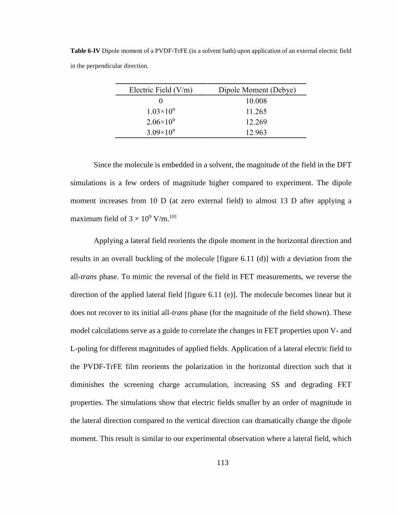
113
Table 6-IV Dipole moment of a PVDF-TrFE (in a solvent bath) upon application of an external electric field
in the perpendicular direction.
Electric Field (V/m) Dipole Moment (Debye)
0 10.008
1.03×10⁹ 11.265
2.06×10⁹ 12.269
3.09×10⁹ 12.963
Since the molecule is embedded in a solvent, the magnitude of the field in the DFT
simulations is a few orders of magnitude higher compared to experiment. The dipole
moment increases from 10 D (at zero external field) to almost 13 D after applying a
maximum field of 3 × 10⁹ V/m.101
Applying a lateral field reorients the dipole moment in the horizontal direction and
results in an overall buckling of the molecule [figure 6.11 (d)] with a deviation from the
all-trans phase. To mimic the reversal of the field in FET measurements, we reverse the
direction of the applied lateral field [figure 6.11 (e)]. The molecule becomes linear but it
does not recover to its initial all-trans phase (for the magnitude of the field shown). These
model calculations serve as a guide to correlate the changes in FET properties upon V- and
L-poling for different magnitudes of applied fields. Application of a lateral electric field to
the PVDF-TrFE film reorients the polarization in the horizontal direction such that it
diminishes the screening charge accumulation, increasing SS and degrading FET
properties. The simulations show that electric fields smaller by an order of magnitude in
the lateral direction compared to the vertical direction can dramatically change the dipole
moment. This result is similar to our experimental observation where a lateral field, which
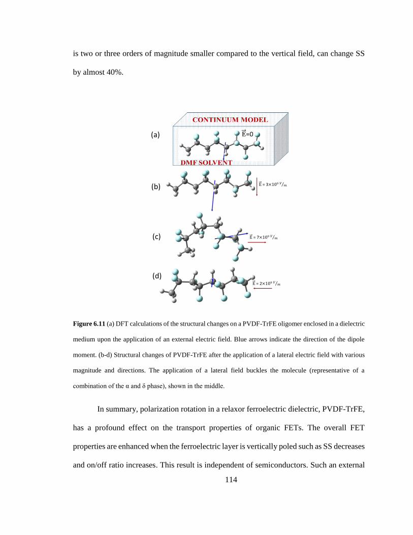
114
is two or three orders of magnitude smaller compared to the vertical field, can change SS
by almost 40%.
Figure 6.11 (a) DFT calculations of the structural changes on a PVDF-TrFE oligomer enclosed in a dielectric
medium upon the application of an external electric field. Blue arrows indicate the direction of the dipole
moment. (b-d) Structural changes of PVDF-TrFE after the application of a lateral electric field with various
magnitude and directions. The application of a lateral field buckles the molecule (representative of a
combination of the α and δ phase), shown in the middle.
In summary, polarization rotation in a relaxor ferroelectric dielectric, PVDF-TrFE,
has a profound effect on the transport properties of organic FETs. The overall FET
properties are enhanced when the ferroelectric layer is vertically poled such as SS decreases
and on/off ratio increases. This result is independent of semiconductors. Such an external
= 3×109
= 7×109
= 2×10⁹
Electric Field(V/m)
Dipole Moment (Debye)
Vertically poled 12.963
5.14×10⁸ 10.669
2.06×10⁹ 10.665
3.09×10⁹ 10.749
5.14×10⁹ 11.082
(a)
(b)
(c)
(d)
115
tuning knob not only benefits an understanding of charge-transport mechanisms in a wide
range of polymeric and molecular semiconductor-based devices but also provides new
design architectures for improving FET performance. By employing low-operating voltage
FETs, we independently exploit the impact of polarization rotation on the FET
characteristics. A caveat for high-operating voltage FETs is that L-poled FETs may behave
like V-poled devices due to polarization inversion in the dielectric layer by the gate voltage
during normal FET operation. A strong effect of polarization modulation may be
envisioned if the transistor architecture is scaled down by reducing channel lengths,
decreasing the distance between the lateral electrodes, and by using thin ferroelectric
dielectric films. Channel lengths in the tens to hundreds of nm range and a thin dielectric
layer (tens of nm) lowers the operating voltage of FETs. Such dimensions may allow poling
of the dielectric layer during the normal operation of the FET, resulting in SS values close
to that of MOSFETs.
A small channel length, which may be achieved by nanolithography, allows the
placement of the lateral electrodes closer than the mm distances used in this work. The
energy needed for polarization rotation will thus be reduced, and one may expect larger
differences in SS and other FET transport properties between V-poled and L-poled devices.
Orienting and reorienting the polarization direction serves as a tuning parameter for
manipulating SS and carrier mobilities in organic FETs. L-poling of a V-poled PVDF-TrFE
film shows changes in carrier transport in FETs as well as reduces the overall capacitance
in MIM structures. SEM images and XRD from poled and unpoled PVDF-TrFE reveal
subtle changes in the microstructure and overall polarization of the PVDF-TrFE film. DFT
calculations of the dipole moment from a molecular unit embedded in a solvent bath show
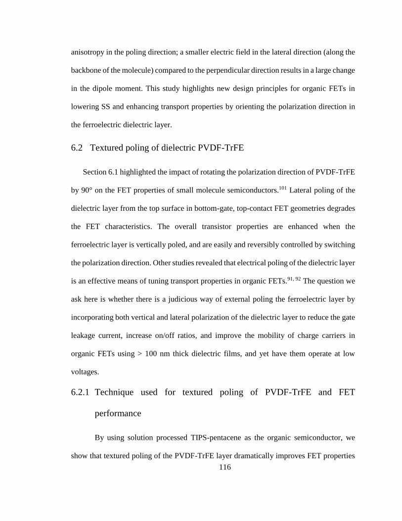
116
anisotropy in the poling direction; a smaller electric field in the lateral direction (along the
backbone of the molecule) compared to the perpendicular direction results in a large change
in the dipole moment. This study highlights new design principles for organic FETs in
lowering SS and enhancing transport properties by orienting the polarization direction in
the ferroelectric dielectric layer.
6.2 Textured poling of dielectric PVDF-TrFE
Section 6.1 highlighted the impact of rotating the polarization direction of PVDF-TrFE
by 90° on the FET properties of small molecule semiconductors.101 Lateral poling of the
dielectric layer from the top surface in bottom-gate, top-contact FET geometries degrades
the FET characteristics. The overall transistor properties are enhanced when the
ferroelectric layer is vertically poled, and are easily and reversibly controlled by switching
the polarization direction. Other studies revealed that electrical poling of the dielectric layer
is an effective means of tuning transport properties in organic FETs.91, 92 The question we
ask here is whether there is a judicious way of external poling the ferroelectric layer by
incorporating both vertical and lateral polarization of the dielectric layer to reduce the gate
leakage current, increase on/off ratios, and improve the mobility of charge carriers in
organic FETs using > 100 nm thick dielectric films, and yet have them operate at low
voltages.
6.2.1 Technique used for textured poling of PVDF-TrFE and FET
performance
By using solution processed TIPS-pentacene as the organic semiconductor, we
show that textured poling of the PVDF-TrFE layer dramatically improves FET properties
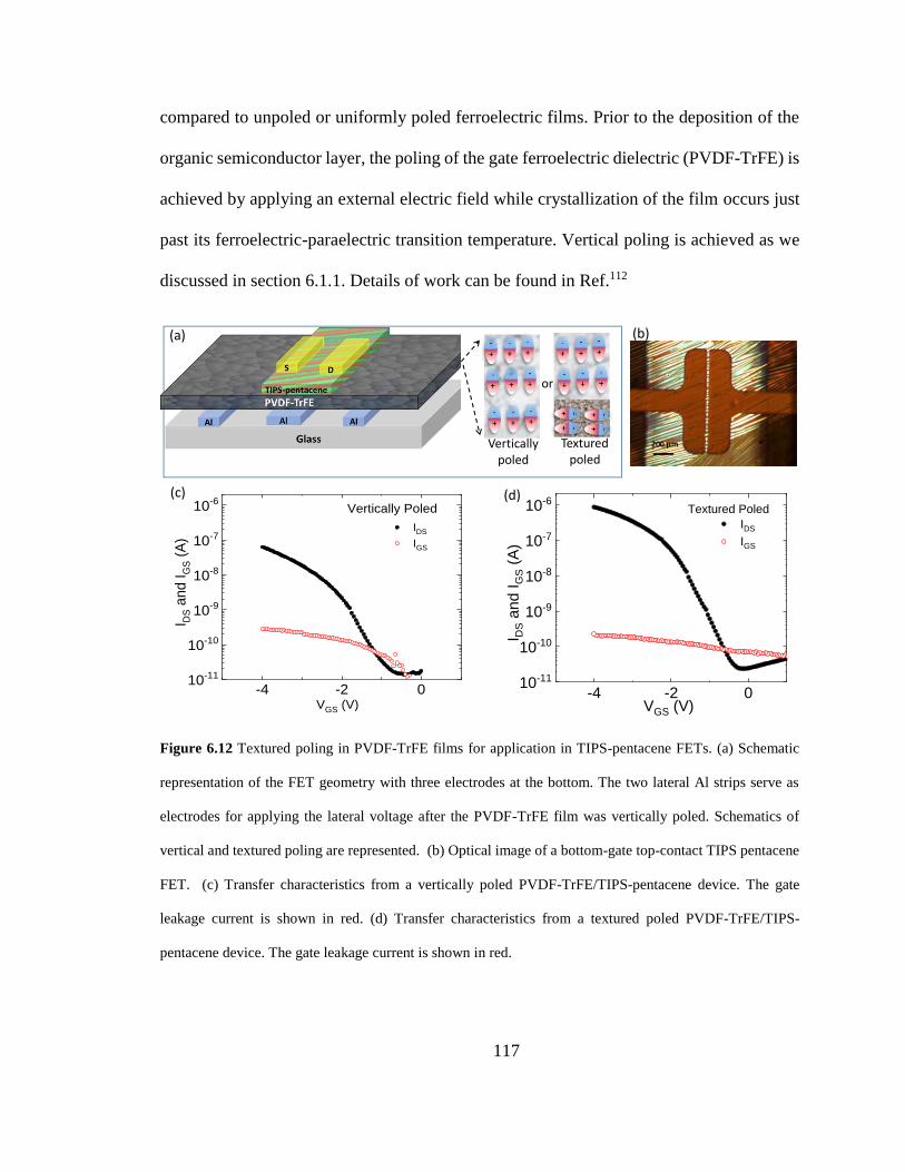
117
compared to unpoled or uniformly poled ferroelectric films. Prior to the deposition of the
organic semiconductor layer, the poling of the gate ferroelectric dielectric (PVDF-TrFE) is
achieved by applying an external electric field while crystallization of the film occurs just
past its ferroelectric-paraelectric transition temperature. Vertical poling is achieved as we
discussed in section 6.1.1. Details of work can be found in Ref.112
Figure 6.12 Textured poling in PVDF-TrFE films for application in TIPS-pentacene FETs. (a) Schematic
representation of the FET geometry with three electrodes at the bottom. The two lateral Al strips serve as
electrodes for applying the lateral voltage after the PVDF-TrFE film was vertically poled. Schematics of
vertical and textured poling are represented. (b) Optical image of a bottom-gate top-contact TIPS pentacene
FET. (c) Transfer characteristics from a vertically poled PVDF-TrFE/TIPS-pentacene device. The gate
leakage current is shown in red. (d) Transfer characteristics from a textured poled PVDF-TrFE/TIPS-
pentacene device. The gate leakage current is shown in red.
Verticallypoled
Texturedpoled
(a) (b)
(c) (d)
or
-4 -2 010-11
10-10
10-9
10-8
10-7
10-6
I DS a
nd
IG
S (
A)
IDS
IGS
Textured Poled
VGS (V)-4 -2 0
10-11
10-10
10-9
10-8
10-7
10-6
IDS
IGS
I DS a
nd I
GS (
A)
VGS (V)
Vertically Poled
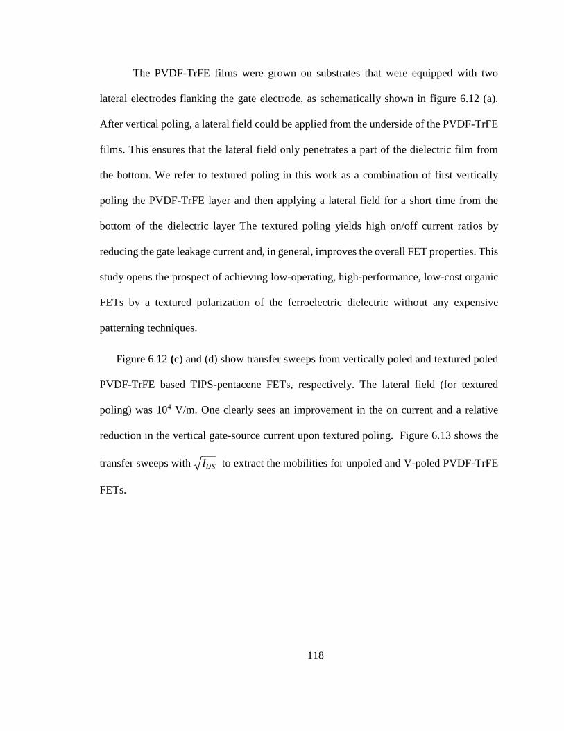
118
The PVDF-TrFE films were grown on substrates that were equipped with two
lateral electrodes flanking the gate electrode, as schematically shown in figure 6.12 (a).
After vertical poling, a lateral field could be applied from the underside of the PVDF-TrFE
films. This ensures that the lateral field only penetrates a part of the dielectric film from
the bottom. We refer to textured poling in this work as a combination of first vertically
poling the PVDF-TrFE layer and then applying a lateral field for a short time from the
bottom of the dielectric layer The textured poling yields high on/off current ratios by
reducing the gate leakage current and, in general, improves the overall FET properties. This
study opens the prospect of achieving low-operating, high-performance, low-cost organic
FETs by a textured polarization of the ferroelectric dielectric without any expensive
patterning techniques.
Figure 6.12 (c) and (d) show transfer sweeps from vertically poled and textured poled
PVDF-TrFE based TIPS-pentacene FETs, respectively. The lateral field (for textured
poling) was 104 V/m. One clearly sees an improvement in the on current and a relative
reduction in the vertical gate-source current upon textured poling. Figure 6.13 shows the
transfer sweeps with √𝐼𝐷𝑆 to extract the mobilities for unpoled and V-poled PVDF-TrFE
FETs.
119
Figure 6.13 Typical transfer and square root of current plots to show how the saturation mobility and
subthreshold swing (SS) parameters were extracted. (a) Transfer characteristics and square root of IDS of a
vertically poled PVDF-TrFE/TIPS-pentacene FET. (b) Transfer characteristics and square root of IDS of a
textured poled PVDF-TrFE/TIPS-pentacene FET.
The best performing textured poled FETs yield mobility of 1 cm2/Vs or higher, on/off
ratio of 105 and a SS of 200 mV/decade whereas the vertically poled FETs yield mobility
0.08 cm2/Vs, on/off ratio of 104 and a SS of 350 mV/decade. On average, the carrier
mobilities are seen to improve by an order of a magnitude for the textured poled devices.
-4 -2 010-11
10-10
10-9
10-8
10-7
mobility= 0.08 cm 2/Vs
on/off = 104
Subthreshold= 550 mV/decadeI D
S(A
)
VGS (V)
Vertically poled0
1
2
I DS
1/2
(A)1
/2
x10-4(a) (b)
-4 -2 0 210-11
10-10
10-9
10-8
10-7
10-6
Textured poled
I DS
(A)
VGS (V)
0
5
10
I DS
1/2
(A)1
/2
X10-4
mobility= 1 cm2/Vs
on/off = 105
Subthreshold= 350 mV/decade
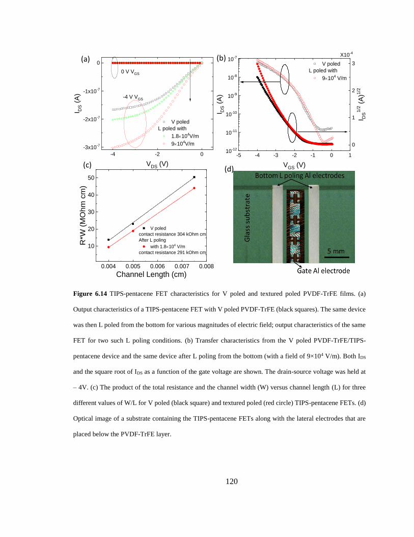
120
Figure 6.14 TIPS-pentacene FET characteristics for V poled and textured poled PVDF-TrFE films. (a)
Output characteristics of a TIPS-pentacene FET with V poled PVDF-TrFE (black squares). The same device
was then L poled from the bottom for various magnitudes of electric field; output characteristics of the same
FET for two such L poling conditions. (b) Transfer characteristics from the V poled PVDF-TrFE/TIPS-
pentacene device and the same device after L poling from the bottom (with a field of 9×10⁴ V/m). Both IDS
and the square root of IDS as a function of the gate voltage are shown. The drain-source voltage was held at
– 4V. (c) The product of the total resistance and the channel width (W) versus channel length (L) for three
different values of W/L for V poled (black square) and textured poled (red circle) TIPS-pentacene FETs. (d)
Optical image of a substrate containing the TIPS-pentacene FETs along with the lateral electrodes that are
placed below the PVDF-TrFE layer.
-5 -4 -3 -2 -1 0 110-12
10-11
10-10
10-9
10-8
10-7
V poled
L poled with
9´104 V/m
I DS (
A)
VGS (V)
0
1
2
3
I DS
1/2
(A
)1/2
X10-4
-4 -2 0
-3x10⁻⁷
-2x10⁻⁷
-1x10⁻⁷
0
V poled
L poled with
1.8´104V/m
9´104V/m
-4 V VGS
I DS (
A)
VDS (V)
0 V VGS
0.004 0.005 0.006 0.007 0.008
10
20
30
40
50
V poled
contact resistance 304 kOhm cm
After L poling
with 1.8´104 V/m
contact resistance 291 kOhm cm
R*W
(M
Ohm
cm
)
Channel Length (cm)
(a) (b)
(c) (d)
121
Figure 6.14 (a) shows the output characteristics of a V-poled FET at VGS of 0 V and -
4V (black square). The same device was then L-poled for different magnitudes of electric
fields for 15 min, and then the FET characteristics were measured. The results after
applying field strengths of 1.8×10⁴ V/m and 9×10⁴ V/m are shown. An improvement in the
FET modulation in the output characteristics is seen after L poling. The transfer curves
from the same V poled FET (as in figure 6.14 (a)) and after L poling the device is shown
in Figure 6.14 (b). The off current (IDS) goes down after L poling along and shows a higher
slope for √𝐼𝐷𝑆 compared to the only V poled FET.
One may ask whether the improvement in FET characteristics after L poling the V-
poled device (textured poling) is related to a change in the contact resistance. Each
substrate supported several FETs with varying W/L ratio as shown in figure 6.14 (d).
Contact resistance normalized with width of the channel (W) is obtained by using the
transmission line method (TLM), commonly used for the calculation of contact resistance
in FETs.113, 114
RW = RCW+L
μCi(VGS−VTh) (6.2)
Where R is total resistance, RC is contact resistance, Ci is the dielectric capacitance, μ is
the carrier mobility, L is the channel length, VGS and VTh are the gate-source and threshold
voltages, respectively. The product of the total resistance and the channel width versus
channel length for three different values of W/L for V-poled (black square) and L poled
with 1.8×10⁴ V/m (red circle) are shown in figure 6.14 (c). The contact resistance (~ 300
kΩ cm) is approximately the same for both conditions of poling, and is at least two orders
of magnitude smaller than the channel resistance. Thus, the differences in the V poled and
122
the textured poled devices arise from an improvement in the dielectric layer itself. It is not
surprising that the contact resistance of TIPS-pentacene FETs here is higher with PVDF-
TrFE compared with other dielectrics found in the literature; it is mainly due to the effect
of polarization fluctuation at the semiconductor-dielectric interface.
6.2.2 Poling field optimization, microscopy and simulation
Next, we look at optimum lateral electric fields required for improving the FET
characteristics. As was shown in Ref.101, lateral poling from the top of the dielectric layer
induces a spontaneous parallel electric field, which greatly increases the off current and
degrades SS and μ. One may expect a similar scenario by L poling from the bottom; if the
electric field is high enough, it may penetrate the bulk of the dielectric layer. Figure 6.15
(a) shows the transfer characteristics for a V poled and after L poling from bottom by
applying an electric field of 105 V/m. Here we clearly see a degradation of transfer
characteristics where the off current is greatly enhanced and VTh is seen to become positive.
What may seem a bit odd at the first glance is the difference between figure 6.15 (a) and
figure 6.15 (b) as the magnitude of the lateral fields are not that different. We point out that
the field distribution here is not uniform. As there is the central gate electrode, the
penetrated field can be quite different at different locations. One expects from Gauss’s law
that right in the middle of the central gate electrode, the electric field is exactly zero. Hence,
if the FETs are slightly displaced from the center of the gate electrode (bright central region
shown in figure 6.15 (d)), the field distribution will be higher. We point out that the FET
in figure 6.15 (a) was more off-centered compared to the device shown in figure 6.14. As
a comparison, we show the transfer characteristics of another V poled FET where it was
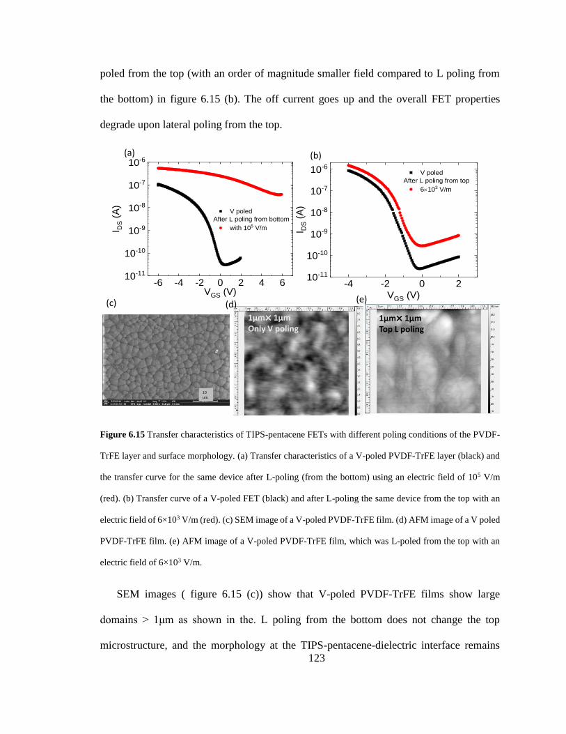
123
poled from the top (with an order of magnitude smaller field compared to L poling from
the bottom) in figure 6.15 (b). The off current goes up and the overall FET properties
degrade upon lateral poling from the top.
Figure 6.15 Transfer characteristics of TIPS-pentacene FETs with different poling conditions of the PVDF-
TrFE layer and surface morphology. (a) Transfer characteristics of a V-poled PVDF-TrFE layer (black) and
the transfer curve for the same device after L-poling (from the bottom) using an electric field of 105 V/m
(red). (b) Transfer curve of a V-poled FET (black) and after L-poling the same device from the top with an
electric field of 6×10³ V/m (red). (c) SEM image of a V-poled PVDF-TrFE film. (d) AFM image of a V poled
PVDF-TrFE film. (e) AFM image of a V-poled PVDF-TrFE film, which was L-poled from the top with an
electric field of 6×10³ V/m.
SEM images ( figure 6.15 (c)) show that V-poled PVDF-TrFE films show large
domains > 1μm as shown in the. L poling from the bottom does not change the top
microstructure, and the morphology at the TIPS-pentacene-dielectric interface remains
-6 -4 -2 0 2 4 610-11
10-10
10-9
10-8
10-7
10-6
V poled
After L poling from bottom
with 105 V/mI DS (
A)
VGS (V)
1μm× 1μmOnly V poling
1μm× 1μmTop L poling
10 μm
(a) (b)
(c) (d)(e)
-4 -2 0 210-11
10-10
10-9
10-8
10-7
10-6 V poled
After L poling from top
6´103 V/m
I DS (
A)
VGS (V)
124
unchanged. These features are discernable even with AFM images at small length scales.
Figure 6.15 (d) shows 1μm×1μm AFM image of a film that was V-poled which is similar
to films that are L-poled from the bottom. Upon L poling from the top, the morphology of
the film is seen to change along with the increase in the off currents. In this work the
processing conditions for depositing TIPS-pentacene was not changed; only the poling
conditions of the dielectric were altered.
We obtained cross-sectional TEM images from V-poled, textured poled and unpoled
PVDF-TrFE films grown on Al coated glass. A focused ion beam (FIB) SEM dual beam
instrument was used for creating a cross-section from the sample, which was subsequently
lifted out of the sample. TEM cross-sections were prepared in the Scios DualBeam via the
Ga ion beam. First, between 0.5-1 μm of Pt was deposited using the electron beam,
followed by 2 μm of Pt deposited using the ion beam. The sample was then trenched to
form a cross-section and cut away from the substrate using the ion beam at 30 kV and
various beam currents. The cross-sections were subsequently lifted out when attached to a
needle within the Scios, and polished from 2 μm to 100 nm using smaller ion beam currents
and voltages as the cross-sections became thinner. Finally, a Ga ion beam with low kV and
low current (2 kV, 15 pA) was employed to further clean off the surface amorphorization
layer. The cross-sections were attached to a copper omniprobe through Pt deposition,
which were then able to be directly loaded onto the TEM single-tilt holder. HRTEM
imaging was conducted in a FEI Tecnai F30 G2 at 100 kV. Beam alignments were
conducted on the glass portion of the cross-sections to minimize beam damage and any
interactions with the PVDF-TrFE film.
125
Figure 6.16 (b)-(e) show the cross-sectional TEM images from textured and
unpoled films grown on Al coated glass, identical to the FETs. The textured poling was
achieved as described earlier. Overall, the bulk of the PVDF-TrFE morphology looks quite
similar for poled and unpoled films. Since the Al layer is also lifted out along with the
PVDF-TrFE, there is an issue of additional poling by the e-beam while imaging near the
Al interface over time. Even then, we find subtle differences between the textured poled
and unpoled films. For the textured poled sample, there is a difference in the morphology
of the PVDF-TrFE film near the Al electrode compared to the bulk as shown in figure 6.16
(b). The initial TEM images show a layer of approximately 30 - 40 nm region near the
electrode with a different morphology, which is lighter in color (highlighted by the blue
box). Upon subsequent measurements, this layer expands from 40 nm to 55 nm due to
additional polarization by the e-beam in the proximity of the Al interface (figure 6.16 (c)).
It is important to note that this narrow layer near the Al electrode is immediately visible in
textured poled TEM images. In contrast, the unpoled sample does not show any difference
in morphology throughout the PVDF-TrFE film in the first few TEM images (figure 6.16
(d)) but over time there is a layer near the Al electrode that looks quite similar to the
textured poled films (figure 6.16 (e)). The TEM measurements yield some insight into the
penetration of the field into the dielectric layer upon textured poling; however, it is difficult
to systematically quantify the extent of lateral poling in the dielectric layer as a function of
the electric field due to additional poling problems. Since textured poling is achieved by
lateral poling after vertical poling, the bottom Al electrode is necessary.
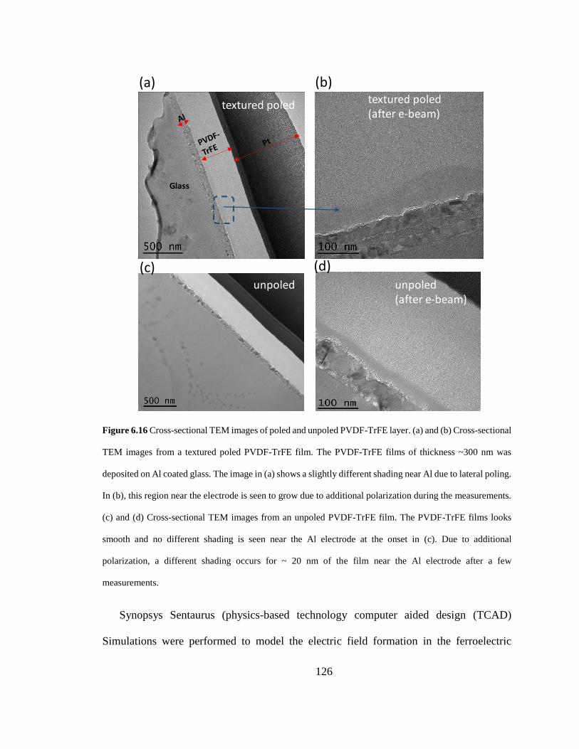
126
Figure 6.16 Cross-sectional TEM images of poled and unpoled PVDF-TrFE layer. (a) and (b) Cross-sectional
TEM images from a textured poled PVDF-TrFE film. The PVDF-TrFE films of thickness ~300 nm was
deposited on Al coated glass. The image in (a) shows a slightly different shading near Al due to lateral poling.
In (b), this region near the electrode is seen to grow due to additional polarization during the measurements.
(c) and (d) Cross-sectional TEM images from an unpoled PVDF-TrFE film. The PVDF-TrFE films looks
smooth and no different shading is seen near the Al electrode at the onset in (c). Due to additional
polarization, a different shading occurs for ~ 20 nm of the film near the Al electrode after a few
measurements.
Synopsys Sentaurus (physics-based technology computer aided design (TCAD)
Simulations were performed to model the electric field formation in the ferroelectric
Glass
unpoled unpoled(after e-beam)
textured poled textured poled (after e-beam)
(a) (b)
(c) (d)
127
dielectric layer. Sentaurus Device has an extensive set of device physics models and is
capable of modeling drift-diffusion, thermodynamic, and hydrodynamic effects in
semiconductor devices. It enables the numeric simulation of electrical behavior at user
defined mesh points using coupled Poisson equation. The meshing scheme for the
simulated device stack, using TCAD, is shown in figure 6.17 (a-b).
The 2-D structure model consisted of 500 μm thick glass substrate with 400 nm thick
dielectric layer. Aluminum source and drain electrodes (25 μm wide, 60 nm thick) were
separated by 550 μm gap. In the center of the device was an unbiased gate contact of the
same dimensions as the source-drain electrode. The dielectric material parameters were
modeled using the generic Insulator2 material file in the Sentaurus suite. The dielectric
constant of this material was changed to 8.3 to better simulate real device. The device was
biased from source to drain using a quasistationary voltage ramp to 20 V with minimum
step size of 10-5 V and maximum step size 0.1V, solving the coupled Poisson electron-hole
formula at each step. The mesh was refined to 100 nm x 100 nm around the length of the
dielectric/Al contacts (refer to Fig. S4). A finer meshing was placed around the central
electrode for high resolution view of absolute electric field (10 nm x 10 nm). The resulting
horizontal electric field was plotted as a function of length at two vertical points in the
dielectric layer.
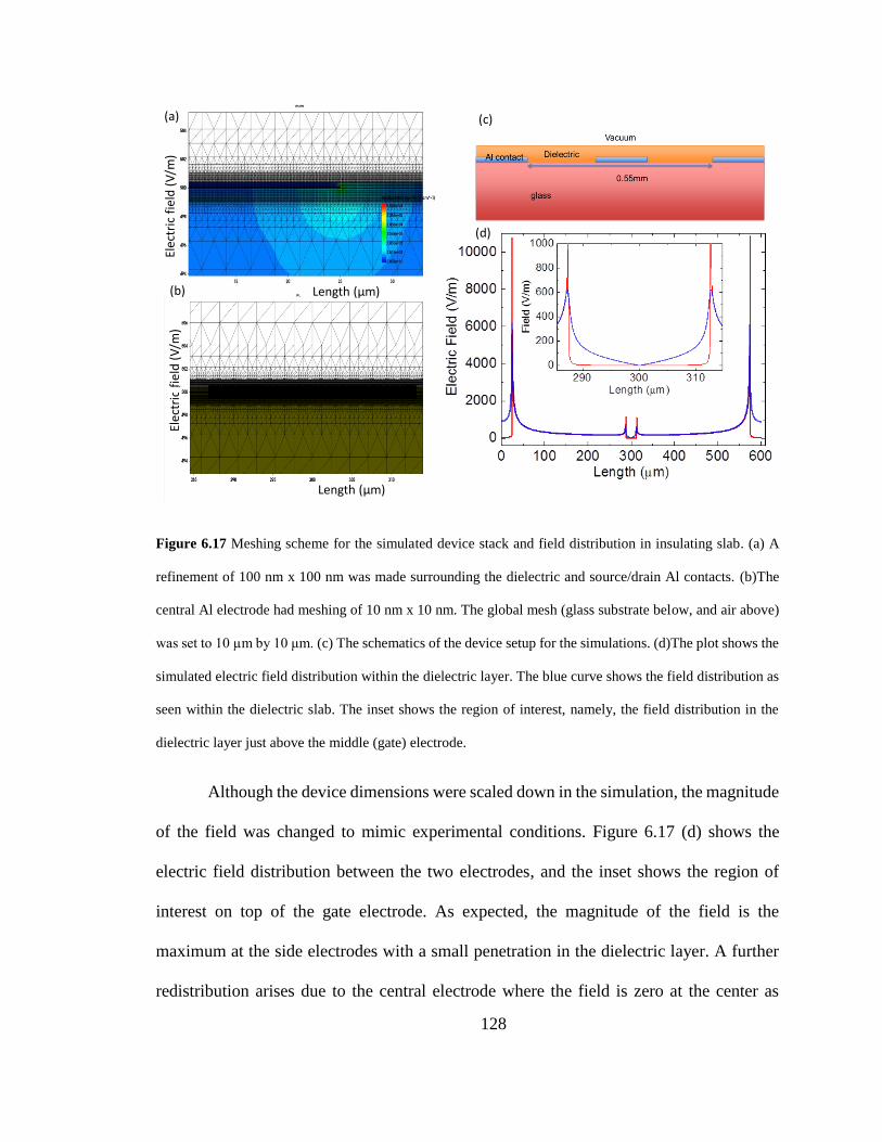
128
Figure 6.17 Meshing scheme for the simulated device stack and field distribution in insulating slab. (a) A
refinement of 100 nm x 100 nm was made surrounding the dielectric and source/drain Al contacts. (b)The
central Al electrode had meshing of 10 nm x 10 nm. The global mesh (glass substrate below, and air above)
was set to 10 µm by 10 μm. (c) The schematics of the device setup for the simulations. (d)The plot shows the
simulated electric field distribution within the dielectric layer. The blue curve shows the field distribution as
seen within the dielectric slab. The inset shows the region of interest, namely, the field distribution in the
dielectric layer just above the middle (gate) electrode.
Although the device dimensions were scaled down in the simulation, the magnitude
of the field was changed to mimic experimental conditions. Figure 6.17 (d) shows the
electric field distribution between the two electrodes, and the inset shows the region of
interest on top of the gate electrode. As expected, the magnitude of the field is the
maximum at the side electrodes with a small penetration in the dielectric layer. A further
redistribution arises due to the central electrode where the field is zero at the center as
Length (µm)
Elec
tric
fie
ld (
V/m
)
(a)
(b)
Length (µm)
Elec
tric
fie
ld (
V/m
)
(c)
(d)
129
shown in the inset of figure 6.17 (d). Viewing from the top of the dielectric layer the field
penetration within the dielectric layer is seen to be roughly 1/3 the value near the edge,
which falls off closer to the center of the electrode [inset of figure 6.17 (d)]. Since the
channel length of the FETs were > 50 μm, it is expected that there will be some influence
of the field roughly at 1/3 of the dielectric layer from the bottom while lateral poling.
Additionally, the simulations only considered a slab of a dielectric with the same κ as
PVDF-TrFE but not a real ferroelectric with spontaneous polarization. The simulations
highlight that if the FETs are away from the center of the gate electrode, the field
penetration is high. This was observed for the FET shown in figure 6.15 (a), where most
likely the entire dielectric layer is laterally polarized with the applied field strength,
destroying the vertical polarization. These observations show that the optimum condition
of textured poling for enhancing the FET characteristics is when the top of the dielectric
(at the semiconductor-insulator interface) is still vertically polarized but only the bottom
1/3-1/4 portion of the dielectric is laterally poled. We further note that the applied electric
fields quoted here are based on the applied voltages to the lateral electrodes; the simulations
show that the actual field felt at the central electrode would be only around 2% of the
applied field or even lower.
In summary, the strategy of textured poling of the polymer ferroelectric layer
dramatically reduces the gate leakage current and enhances transport in organic FETs. By
applying a lateral electric field near the gate electrode to an already vertically poled PVDF-
TrFE layer, the on/off ratios are found to be upwards of 105 in TIPS-pentacene FETs.
Carrier mobilities measured under ambient conditions are an order of magnitude higher for
textured poled TIPS-pentacene FETs compared to vertically poled FETs. Without any

130
specific processing of the TIPS-pentacene films and using the strategy of only textured
poling the ferroelectric dielectric, ambient condition μFET (holes) easily reaches 1 cm2/Vs.
131
7 Summary and suggested future works
7.1 Summary
In this thesis we showed that the ferroelectric dielectric PVDF-TrFE, where the
polarization strength can be tuned with temperature, provides a mechanism for
understanding charge transport in the rapidly growing field of small molecule and polymer-
based thin film transistors. The charge transport in ferroelectric-based organic FETs is
strongly influenced by a polarization dominant transport rather than an energetic disorder
within the framework of a hopping transport. When the gate insulator is sufficiently polar,
Fröhlich polarons play an important role in interfacial transport. This effect is more
pronounced for thinner dielectric films. By fabricating stacked PVDF-TrFE/SiO2
dielectrics, the surface between pentacene and PVDF-TrFE remains unchanged but since
the gate electrode is in contact with the SiO2 layer, the polarization field is absent. By
comparing the stacked devices with single layer PVDF-TrFE pentacene OFETs,
temperature-dependent mobility due to the polarization fluctuation due to the dielectric
layer was extracted.
Drop-casted TIPS-pentacene films exhibit single-trap-level SCLC, similar to high-
purity crystalline organic molecules. The origin of these traps could be structural or other
chemical defects, which typically give rise to discrete trap states and may occur at the grain
boundaries. A bulk-transport measurement from TIPS-pentacene clearly shows a negative
coefficient of mobility beyond 180 K. A similar behavior is seen in FET transport when a
ferroelectric dielectric, PVDF-TrFE, is used. As such, the FET mobilities are lower than
the minimum condition mobility required for observing disorder-free transport, yet the
132
presence of a polarization field of the ferroelectric dielectric results in a transport
mechanism, mimicking band-like transport beyond 200 K. This is attributed to an ease of
a de-trapping mechanism owing to the nature of discrete traps. This paves the way for
exploring band-like transport (dμ/dT < 0) in other solution-processable π-conjugated
molecules and polymers with discrete trap levels by utilizing ferroelectric dielectrics in
FET geometries.
We demonstrated that the dipole engineering of the ferroelectric dielectric PVDF-
TrFE enhances FET properties in particular the subthreshold swing can change by an order
of magnitude, and the carrier mobility is enhanced by two order of magnitude. Polarization
rotation in PVDF-TrFE has a profound effect on the transport properties of organic FETs.
The subthreshold swing decreases, and the overall FET properties are enhanced when the
ferroelectric layer is vertically poled with an external field. The direction of polarization
for the V-poled PVDF-TrFE film is chosen such that it is in the same direction as the gate
electric field, boosting the screening charge accumulation in the channel region.
Irrespective of the organic semiconductor layer in the FET, results show that polarization
orientation in the polymer ferroelectric layer directly controls FET performance. Orienting
and reorienting the polarization direction serves as a tuning parameter for manipulating SS
and carrier mobilities in organic FETs. L-poling of a V-poled PVDF-TrFE film shows
changes in carrier transport in FETs as well as reduces the overall capacitance in MIM
structures. This study highlights new design principles for organic FETs in lowering SS
and enhancing transport properties by orienting the polarization direction in the
ferroelectric dielectric layer. It has also been demonstrated that the strategy of textured
poling of the polymer ferroelectric layer dramatically reduces the gate leakage current and
133
enhances transport in organic FETs. The texturing achieved by first vertically poling the
PVDF-TrFE film and then laterally poling close to the gate electrode results in improved
mobility, on/off ratio, and subthreshold swing. TIPS-pentacene FETs, for example, show
an improvement of more than an order of magnitude in carrier mobility and on/off ratio
under ambient condition and operating voltages below -4 V. This study opens the prospect
of achieving low-operating, high-performance, low-cost organic FETs by a textured
polarization of the ferroelectric dielectric without any expensive patterning techniques.
7.2 Suggested future works
7.2.1 Fast switching organic FETs by dipole engineering of PVDF-TrFE
In chapter 6 we saw that dipole engineering of PVDF-TrFE with external field
results in improved FET properties. We wish to expand the study on dipole engineering
of ferroelectric polymers such as PVDF-TrFE to enhance the switching time in organic
FETs. Low-cost, large area, solution processed, thin film polymer transistors are emerging
as a next-generation technology, allowing electronic components to be integrated into
flexible substrates. However, polymer thin film transistors suffer from low switching times,
rendering their use in analytical and digital logic circuits problematic. Fast switching times
in polymer transistors may be achieved by miniaturizing the device size, but this requires
nanolithography, which is impractical for polymers and low-cost fabrication methods like
printing. It would be worthwhile to utilize low-cost strategies for materials engineering to
improve switching times by orders of magnitude compared to the present state-of-the-art
thin film polymer transistors, which will open up the polymer circuit technology for many
new applications. An experimental method based on a comparative study on unpoled,
134
vertically poled and textured poled PVDF-TrFE FETs may be fabricated and characterized
to get the crucial parameters that controls switching time. The transistor switching speed
and the frequency bandwidth measurement can be obtained as described in previous
works.115
As a further extension of this work, the switching times in FETs could be enhanced
by optimized dipole engineering of PVDF-TrFE. Dipole engineering of the dielectric layer,
using low-cost solvent processing and poling polymer ferroelectric dielectrics with external
field, is likely to have a transformative impact on technology where fast switching times
may be realized in long-channel printable thin film organic field-effect transistors and logic
circuits.
7.2.2 Carrier transport mechanism and FET mobility using non-linear optics
In our research, we use current-voltage measurements and analyze data to extract
charge mobility in an organic FET. This method involves the contribution of contact
resistance, the size and geometry of device, and the property of dielectric. Alternative
methods could be developed which does not involve contact resistance, or the influence of
dielectrics. Nonlinear optical methods such as Time-resolved microscopic optical second
harmonic generation (TRM-SHG) and Transient electric field-induced second-harmonic
generation (EFISHG) are well known to probe the carrier mobility and dynamical carrier
transport in organic semiconductors.116-120
The TRM-SHG approach, based on the second order susceptibility, gives
information about the charge transport motion without considering the effect of the
electrode injection process. It is free from the issues of contact resistance. This technique
135
allows selective and direct probing of dynamic carrier motion in organic semiconductor
materials. This technique reveals the dynamic changes in SHG intensity profiles. The
TRM-SHG images can be directly visualized using a charge-coupled device (CCD)
camera. Carrier mobility in semiconductors is estimated by using76,
𝜇 = (1
2
𝑥2
(𝑉−𝑉𝑑𝑟𝑜𝑝)𝜏), (7.1)
where x is the distance from the edge of the source electrode to the front edge of the SHG
emission called transported carrier distance. V is the external voltage applied to the source
electrode and Vdrop is the potential drop. The time delay, τ, is the delay between the laser
pulse and the voltage pulse. The current setup has some limitations and we hope to build
the imaging part of the setup using a CCD and a microscope attachment.
EFISHG, based on the third-order susceptibility, allows direct and selective probing
of dynamic carrier motion in field-effect transistors. Under the application of some DC
field and irradiation of a laser light on the organic materials, the nonlinear polarization, P,
will induce an interaction between electromagnetic fields and electrons in the organic
materials. This is a basic principle of EFISHG measurement. As the electron distribution
of molecules is distorted by the presence of the dc field E(0), this type of nonlinear
polarization is induced even in a centrosymmetric molecular system and P(2ω) can, be
presented by equation,
𝑃(2𝜔) = 𝜒3(2𝜔; 0, 𝜔, 𝜔)𝐸(0)𝐸𝑖(𝜔)𝐸𝑗(𝜔), (7.2)
where χ3 is the third-order-nonlinear susceptibility and E(0) is a local electrostatic field. Ei
and Ej represent the electric field of incident light. EFISHG enables the probing of the
electric field distribution in the FET channel and generates the signals that follow above
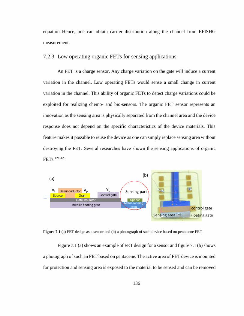
136
equation. Hence, one can obtain carrier distribution along the channel from EFISHG
measurement.
7.2.3 Low operating organic FETs for sensing applications
An FET is a charge sensor. Any charge variation on the gate will induce a current
variation in the channel. Low operating FETs would sense a small change in current
variation in the channel. This ability of organic FETs to detect charge variations could be
exploited for realizing chemo- and bio-sensors. The organic FET sensor represents an
innovation as the sensing area is physically separated from the channel area and the device
response does not depend on the specific characteristics of the device materials. This
feature makes it possible to reuse the device as one can simply replace sensing area without
destroying the FET. Several researches have shown the sensing applications of organic
FETs.121-123
Figure 7.1 (a) FET design as a sensor and (b) a photograph of such device based on pentacene FET
Figure 7.1 (a) shows an example of FET design for a sensor and figure 7.1 (b) shows
a photograph of such an FET based on pentacene. The active area of FET device is mounted
for protection and sensing area is exposed to the material to be sensed and can be removed
VS VDVC Sensing part
Floating gate
control gate
Sensing area
(a)(b)
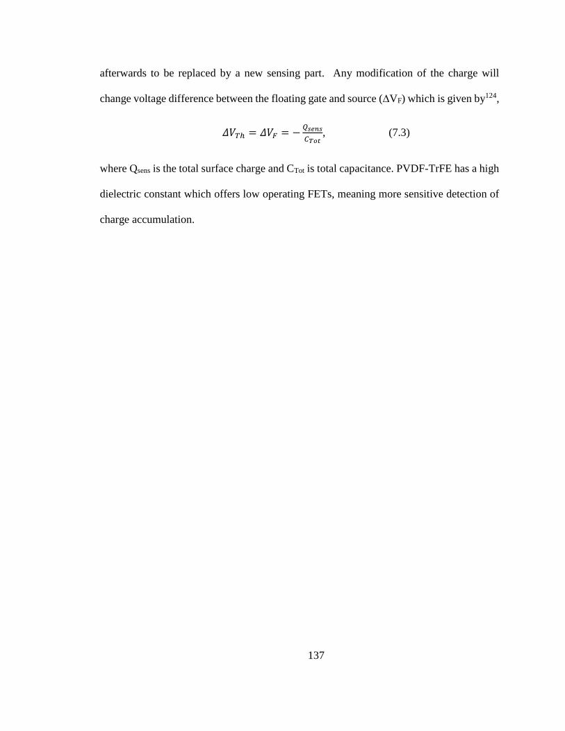
137
afterwards to be replaced by a new sensing part. Any modification of the charge will
change voltage difference between the floating gate and source (∆VF) which is given by124,
𝛥𝑉𝑇ℎ = 𝛥𝑉𝐹 = −𝑄𝑠𝑒𝑛𝑠
𝐶𝑇𝑜𝑡, (7.3)
where Qsens is the total surface charge and CTot is total capacitance. PVDF-TrFE has a high
dielectric constant which offers low operating FETs, meaning more sensitive detection of
charge accumulation.
138
References
1. Chiang, C. K.; Fincher, C. R.; Park, Y. W.; Heeger, A. J.; Shirakawa, H.; Louis,
E. J.; Gau, S. C.; MacDiarmid, A. G., Electrical Conductivity in Doped Polyacetylene.
Phys. Rev. Lett. 1977, 39 (17), 1098-1101.
2. Tsumura, A., applied physic letters 1986, 49, 2.
3. Khan, S. U. M., Organic Semiconductors. Salem Press: 2013.
4. Kim, J. H.; Yun, S. W.; An, B.-K.; Han, Y. D.; Yoon, S.-J.; Joo, J.; Park, S. Y.,
Remarkable Mobility Increase and Threshold Voltage Reduction in Organic Field-Effect
Transistors by Overlaying Discontinuous Nano-Patches of Charge-Transfer Doping Layer
on Top of Semiconducting Film. 2013, 25 (5), 719-724.
5. Xu, W.; Rhee, S.-W., Low-operating voltage organic field-effect transistors with
high-k cross-linked cyanoethylated pullulan polymer gate dielectrics. Journal of Materials
Chemistry 2009, 19 (29), 5250-5257.
6. Gundlach, D. J.; Lin, Y. Y.; Jackson, T. N.; Nelson, S. F.; Schlom, D. G.,
Pentacene organic thin-film transistors-molecular ordering and mobility. IEEE Electron
Device Letters 1997, 18 (3), 87-89.
7. Dinca, L. E.; De Marchi, F.; MacLeod, J. M.; Lipton-Duffin, J.; Gatti, R.; Ma,
D.; Perepichka, D. F.; Rosei, F., Pentacene on Ni(111): room-temperature molecular
packing and temperature-activated conversion to graphene. Nanoscale 2015, 7 (7), 3263-
3269.
139
8. Yamamoto, T.; Takimiya, K., Facile Synthesis of Highly π-Extended Heteroarenes,
Dinaphtho[2,3-b:2‘,3‘-f]chalcogenopheno[3,2-b]chalcogenophenes, and Their
Application to Field-Effect Transistors. J. Am. Chem. Soc. 2007, 129 (8), 2224-2225.
9. Zschieschang, U.; Ante, F.; Kälblein, D.; Yamamoto, T.; Takimiya, K.;
Kuwabara, H.; Ikeda, M.; Sekitani, T.; Someya, T.; Nimoth, J. B.; Klauk, H.,
Dinaphtho[2,3-b:2′,3′-f]thieno[3,2-b]thiophene (DNTT) thin-film transistors with
improved performance and stability. Organic Electronics 2011, 12 (8), 1370-1375.
10. Park, S. K.; Jackson, T. N.; Anthony, J. E.; Mourey, D. A., High mobility solution
processed 6,13-bis(triisopropyl-silylethynyl) pentacene organic thin film transistors.
Applied Physics Letters 2007, 91 (6), 063514.
11. Park, J. G.; Vasic, R.; Brooks, J. S.; Anthony, J. E., Characterization of
functionalized pentacene field-effect transistors and its logic gate application. J. Appl.
Phys. 2006, 100 (4), 044511.
12. Sakanoue, T.; Sirringhaus, H., Band-like temperature dependence of mobility in
a solution-processed organic semiconductor. Nat Mater 2010, 9 (9), 736-740.
13. Davi, N. F. M. a. E. A., Electronic Processes in Non-crystalline Materials. second
ed.; 1979.
14. Klauk, H., Organic thin-film transistors. Chemical Society Reviews 2010, 39 (7),
2643-2666.
15. Zaumseil, J.; Sirringhaus, H., Electron and Ambipolar Transport in Organic Field-
Effect Transistors. Chem. Rev. 2007, 107 (4), 1296-1323.
16. Vissenberg, M. C. J. M.; Matters, M., Theory of the field-effect mobility in
amorphous organic transistors. Physical Review B 1998, 57 (20), 12964-12967.
140
17. Koh, S. E.; Delley, B.; Medvedeva, J. E.; Facchetti, A.; Freeman, A. J.; Marks,
T. J.; Ratner, M. A., Quantum Chemical Analysis of Electronic Structure and n- and p-
Type Charge Transport in Perfluoroarene-Modified Oligothiophene Semiconductors. The
Journal of Physical Chemistry B 2006, 110 (48), 24361-24370.
18. Chesterfield, R. J.; McKeen, J. C.; Newman, C. R.; Frisbie, C. D.; Ewbank, P.
C.; Mann, K. R.; Miller, L. L., Variable temperature film and contact resistance
measurements on operating n-channel organic thin film transistors. J. Appl. Phys. 2004, 95
(11), 6396-6405.
19. Waragai, K.; Akimichi, H.; Hotta, S.; Kano, H.; Sakaki, H., Charge transport in
thin films of semiconducting oligothiophenes. Physical Review B 1995, 52 (3), 1786-1792.
20. Horowitz, G., Organic thin film transistors: From theory to real devices. J. Mater.
Res. 2004, 19 (7), 1946-1962.
21. Jurchescu, O. D.; Baas, J.; Palstra, T. T. M., Effect of impurities on the mobility
of single crystal pentacene. 2004, 84 (16), 3061-3063.
22. Kittel, C., Introduction to Solid State Physics. Book 2004, 8th editioh, 704.
23. Lovinger, A. J., Ferroelectric Polymers. Science 1983, 220 (4602), 1115-1121.
24. Oliveira, F.; Leterrier, Y.; Månson, J.-A.; Sereda, O.; Neels, A.; Dommann, A.;
Damjanovic, D., Process influences on the structure, piezoelectric, and gas-barrier
properties of PVDF-TrFE copolymer. Journal of Polymer Science Part B: Polymer Physics
2014, 52 (7), 496-506.
25. Furukawa, T., Piezoelectricity and pyroelectricity in polymers. IEEE Transactions
on Electrical Insulation 1989, 24 (3), 375-394.
141
26. Li, M.; Wondergem, H. J.; Spijkman, M.-J.; Asadi, K.; Katsouras, I.; Blom, P.
W. M.; de Leeuw, D. M., Revisiting the δ-phase of poly(vinylidene fluoride) for solution-
processed ferroelectric thin films. Nature Materials 2013, 12, 433.
27. G., A. I.; F., M. N., 1969, 18, 41.
28. Laudari, A.; Guha, S., Polarization-induced transport in ferroelectric organic field-
effect transistors. Journal of Applied Physics 2015, 117 (10), 105501.
29. Nan, C.-W.; Weng, G. J., Influence of polarization orientation on the effective
properties of piezoelectric composites. J. Appl. Phys. 2000, 88 (1), 416-423.
30. Khanra, S.; Ghosh, K.; Ferreira, F. F.; Alves, W. A.; Punzo, F.; Yu, P.; Guha,
S., Probing nonlinear optical coefficients in self-assembled peptide nanotubes. Physical
Chemistry Chemical Physics 2017, 19 (4), 3084-3093.
31. Berge, B.; Wicker, A.; Lajzerowicz, J.; Legrand, J. F., Second-Harmonic
Generation of Light and Evidence of Phase Matching in Thin Films of P(VDF-TrFE)
Copolymers. EPL (Europhysics Letters) 1989, 9 (7), 657.
32. Dong-Jin, P.; Jaehyun, M.; Byung-Ok, P., An Analysis on the Electrical Short in a
Large Area Organic Thin Film Transistor Array with the Poly(4-vinylphenol) Gate
Dielectrics. Jpn. J. Appl. Phys. 2009, 48 (8R), 081504.
33. P. Parisse, S. P., M. Passacantando, L. Ottaviano, Thin Sol. Films 2007, 515, 8316.
34. Simon M. Sze, K. K. N., Physics of Semiconductor Devices. 2006, 832.
35. Qi, Y.; Rappe, A. M., Designing Ferroelectric Field-Effect Transistors Based on
the Polarization-Rotation Effect for Low Operating Voltage and Fast Switching. Physical
Review Applied 2015, 4 (4), 044014.
142
36. Zschieschang, U.; Bader, V. P.; Klauk, H., Below-one-volt organic thin-film
transistors with large on/off current ratios. Organic Electronics 2017, 49, 179-186.
37. Zschieschang, U.; Klauk, H., Low-voltage organic transistors with steep
subthreshold slope fabricated on commercially available paper. Organic Electronics 2015,
25, 340-344.
38. Blülle, B.; Häusermann, R.; Batlogg, B., Approaching the Trap-Free Limit in
Organic Single-Crystal Field-Effect Transistors. Physical Review Applied 2014, 1 (3),
034006.
39. Ben Streetman, S. B., Solid State Electronic Devices book 2006.
40. Adil, D. Light scattering studies of organic field effect transistors. University of
Missouri, 2013.
41. CRC Handbook of Chemistry and Physics, 84th Edition Edited by David R. Lide
(National Institute of Standards and Technology). CRC Press LLC: Boca Raton. 2003.
2616 pp. $139.95. ISBN 0-8493-0484-9. J. Am. Chem. Soc. 2004, 126 (5), 1586-1586.
42. Coropceanu, V.; Cornil, J.; da Silva Filho, D. A.; Olivier, Y.; Silbey, R.; Brédas,
J.-L., Charge Transport in Organic Semiconductors. Chem. Rev. 2007, 107 (4), 926-952.
43. Houili, H.; Picon, J. D.; Zuppiroli, L.; Bussac, M. N., Polarization effects in the
channel of an organic field-effect transistor. J. Appl. Phys. 2006, 100 (2), 023702.
44. Konezny, S. J.; Bussac, M. N.; Zuppiroli, L., Hopping and trapping mechanisms
in organic field-effect transistors. Physical Review B 2010, 81 (4), 045313.
45. Naber, R. C. G.; Blom, P. W. M.; Marsman, A. W.; de Leeuw, D. M., Low voltage
switching of a spin cast ferroelectric polymer. Appl. Phys. Lett. 2004, 85 (11), 2032-2034.
143
46. Naber, R. C. G.; Tanase, C.; Blom, P. W. M.; Gelinck, G. H.; Marsman, A. W.;
Touwslager, F. J.; Setayesh, S.; de Leeuw, D. M., High-performance solution-processed
polymer ferroelectric field-effect transistors. Nat Mater 2005, 4 (3), 243-248.
47. Fujisaki, S.; Ishiwara, H.; Fujisaki, Y., Low-voltage operation of ferroelectric
poly(vinylidene fluoride-trifluoroethylene) copolymer capacitors and metal-ferroelectric-
insulator-semiconductor diodes. Applied Physics Letters 2007, 90 (16), 162902.
48. Nguyen, C. A.; Mhaisalkar, S. G.; Ma, J.; Lee, P. S., Enhanced organic
ferroelectric field effect transistor characteristics with strained poly(vinylidene fluoride-
trifluoroethylene) dielectric. Organic Electronics 2008, 9 (6), 1087-1092.
49. Zheng, Y.; Ni, G.-X.; Toh, C.-T.; Tan, C.-Y.; Yao, K.; Özyilmaz, B., Graphene
Field-Effect Transistors with Ferroelectric Gating. Phys. Rev. Lett. 2010, 105 (16), 166602.
50. Bässler, H., Charge Transport in Disordered Organic Photoconductors a Monte
Carlo Simulation Study. physica status solidi (b) 1993, 175 (1), 15-56.
51. Hulea, I. N.; Fratini, S.; Xie, H.; Mulder, C. L.; Iossad, N. N.; Rastelli, G.;
Ciuchi, S.; Morpurgo, A. F., Tunable Frohlich polarons in organic single-crystal
transistors. Nat Mater 2006, 5 (12), 982-986.
52. Xia, Y.; Cho, J. H.; Lee, J.; Ruden, P. P.; Frisbie, C. D., Comparison of the
Mobility–Carrier Density Relation in Polymer and Single-Crystal Organic Transistors
Employing Vacuum and Liquid Gate Dielectrics. Advanced Materials 2009, 21 (21), 2174-
2179.
53. Senanayak, S. P.; Guha, S.; Narayan, K. S., Polarization fluctuation dominated
electrical transport processes of polymer-based ferroelectric field effect transistors.
Physical Review B 2012, 85 (11), 115311.
144
54. Knipp, D.; Street, R. A.; Völkel, A.; Ho, J., Pentacene thin film transistors on
inorganic dielectrics: Morphology, structural properties, and electronic transport. J. Appl.
Phys. 2003, 93 (1), 347-355.
55. Guo, D.; Miyadera, T.; Ikeda, S.; Shimada, T.; Saiki, K., Analysis of charge
transport in a polycrystalline pentacene thin film transistor by temperature and gate bias
dependent mobility and conductance. Journal of Applied Physics 2007, 102 (2), 023706.
56. Dunn, L.; Dodabalapur, A., Temperature dependent transient velocity and mobility
studies in an organic field effect transistor. J. Appl. Phys. 2010, 107 (11), 113714.
57. Gundlach, D. J.; Royer, J. E.; Park, S. K.; Subramanian, S.; Jurchescu, O. D.;
Hamadani, B. H.; Moad, A. J.; Kline, R. J.; Teague, L. C.; Kirillov, O.; Richter, C. A.;
Kushmerick, J. G.; Richter, L. J.; Parkin, S. R.; Jackson, T. N.; Anthony, J. E., Contact-
induced crystallinity for high-performance soluble acene-based transistors and circuits.
Nature Materials 2008, 7, 216.
58. Monroe, D., Hopping in Exponential Band Tails. Phys. Rev. Lett. 1985, 54 (2), 146-
149.
59. Ukah, N. B.; Granstrom, J.; Sanganna Gari, R. R.; King, G. M.; Guha, S., Low-
operating voltage and stable organic field-effect transistors with poly (methyl
methacrylate) gate dielectric solution deposited from a high dipole moment solvent.
Applied Physics Letters 2011, 99 (24), 243302.
60. Knotts, G.; Bhaumik, A.; Ghosh, K.; Guha, S., Enhanced performance of
ferroelectric-based all organic capacitors and transistors through choice of solvent. Appl.
Phys. Lett. 2014, 104 (23), 233301.
61. W., X.; S.-W., R., 2009, 19, 5250.
145
62. Tashiro, K.; Itoh, Y.; Kobayashi, M.; Tadokoro, H., Polarized Raman spectra and
LO-TO splitting of poly(vinylidene fluoride) crystal form I. Macromolecules 1985, 18
(12), 2600-2606.
63. Nakhmanson, S. M.; Korlacki, R.; Johnston, J. T.; Ducharme, S.; Ge, Z.; Takacs,
J. M., Vibrational properties of ferroelectric $\ensuremath{\beta}$-vinylidene fluoride
polymers and oligomers. Physical Review B 2010, 81 (17), 174120.
64. Tashiro, K.; Kobayashi, M., Vibrational spectroscopic study of the ferroelectric
phase transition in vinylidene fluoride-trifluoroethylene copolymers: 1. Temperature
dependence of the Raman spectra. Polymer 1988, 29 (3), 426-436.
65. Adil, D.; Guha, S., Surface-enhanced Raman spectroscopic studies of the Au-
pentacene interface: A combined experimental and theoretical investigation. The Journal
of Chemical Physics 2013, 139 (4), 044715.
66. Mott, N. F.; Davis, E. A., Electronic processes in non-crystalline materials.
Clarendon Press ; Oxford University Press: Oxford; New York, 1979.
67. Miller, A.; Abrahams, E., Impurity Conduction at Low Concentrations. Phys. Rev.
1960, 120 (3), 745-755.
68. Borsenberger, P. M.; Pautmeier, L.; Bässler, H., Charge transport in disordered
molecular solids. The Journal of Chemical Physics 1991, 94 (8), 5447-5454.
69. Pope, M.; Swenberg, C. E., Electronic Processes in Organic Crystals and Polymer.
Second ed.; Oxford University Press: Oxford, 1999.
70. Arif, M.; Yun, M.; Gangopadhyay, S.; Ghosh, K.; Fadiga, L.; Galbrecht, F.;
Scherf, U.; Guha, S., Polyfluorene as a model system for space-charge-limited conduction.
Physical Review B 2007, 75 (19), 195202.
146
71. Chua, L.-L.; Zaumseil, J.; Chang, J.-F.; Ou, E. C. W.; Ho, P. K. H.; Sirringhaus,
H.; Friend, R. H., General observation of n-type field-effect behaviour in organic
semiconductors. Nature 2005, 434 (7030), 194-199.
72. Podzorov, V.; Menard, E.; Rogers, J. A.; Gershenson, M. E., Hall Effect in the
Accumulation Layers on the Surface of Organic Semiconductors. Phys. Rev. Lett. 2005, 95
(22), 226601.
73. Jun, T.; Kazuhito, T.; Yoshinobu, A.; Taishi, T.; Yoshihiro, I., Hall Effect of
Quasi-Hole Gas in Organic Single-Crystal Transistors. Japanese Journal of Applied
Physics 2005, 44 (11L), L1393.
74. Meneau, A. Y. B.; Olivier, Y.; Backlund, T.; James, M.; Breiby, D. W.;
Andreasen, J. W.; Sirringhaus, H., Temperature Dependence of Charge Localization in
High-Mobility, Solution-Crystallized Small Molecule Semiconductors Studied by Charge
Modulation Spectroscopy. Advanced Functional Materials 2015, doi:
10.1002/adfm.201502502.
75. Fratini, S.; Ciuchi, S., Bandlike Motion and Mobility Saturation in Organic
Molecular Semiconductors. Phys. Rev. Lett. 2009, 103 (26), 266601.
76. Kohei, M.; Takaaki, M.; Mitsumasa, I., Band-like transport observed in TIPS-
pentacene thin film by time-resolved microscopic optical second-harmonic generation
imaging. Applied Physics Express 2015, 8 (4), 041601.
77. Stafstrom, S., Electron localization and the transition from adiabatic to
nonadiabatic charge transport in organic conductors. Chemical Society Reviews 2010, 39
(7), 2484-2499.
147
78. Chen, Y.; Yi, H. T.; Podzorov, V., High-Resolution ac Measurements of the Hall
Effect in Organic Field-Effect Transistors. Physical Review Applied 2016, 5 (3), 034008.
79. Yi, H. T.; Gartstein, Y. N.; Podzorov, V., Charge carrier coherence and Hall effect
in organic semiconductors. Scientific Reports 2016, 6, 23650.
80. Schein, L. B.; Duke, C. B.; McGhie, A. R., Observation of the Band-Hopping
Transition for Electrons in Naphthalene. Phys. Rev. Lett. 1978, 40 (3), 197-200.
81. Wang, L. J.; Peng, Q.; Li, Q. K.; Shuai, Z., Roles of inter- and intramolecular
vibrations and band-hopping crossover in the charge transport in naphthalene crystal. The
Journal of Chemical Physics 2007, 127 (4), 044506.
82. Wang, L.; Prezhdo, O. V.; Beljonne, D., Mixed quantum-classical dynamics for
charge transport in organics. Physical Chemistry Chemical Physics 2015, 17 (19), 12395-
12406.
83. Senanayak, S. P.; Narayan, K. S., Strategies for Fast-Switching in All-Polymer
Field Effect Transistors. Advanced Functional Materials 2014, 24 (22), 3324-3331.
84. Naber, R. C. G.; Mulder, M.; de Boer, B.; Blom, P. W. M.; de Leeuw, D. M.,
High charge density and mobility in poly(3-hexylthiophene) using a polarizable gate
dielectric. Organic Electronics 2006, 7 (3), 132-136.
85. Brondijk, J. J.; Asadi, K.; Blom, P. W. M.; de Leeuw, D. M., Physics of organic
ferroelectric field-effect transistors. Journal of Polymer Science Part B: Polymer Physics
2012, 50 (1), 47-54.
86. Zirkl, M.; Sawatdee, A.; Helbig, U.; Krause, M.; Scheipl, G.; Kraker, E.;
Ersman, P. A.; Nilsson, D.; Platt, D.; Bodö, P.; Bauer, S.; Domann, G.; Stadlober, B.,
An All-Printed Ferroelectric Active Matrix Sensor Network Based on Only Five Functional
148
Materials Forming a Touchless Control Interface. Advanced Materials 2011, 23 (18), 2069-
2074.
87. Lee, J.-H.; Yoon, H.-J.; Kim, T. Y.; Gupta, M. K.; Lee, J. H.; Seung, W.; Ryu,
H.; Kim, S.-W., Micropatterned P(VDF-TrFE) Film-Based Piezoelectric Nanogenerators
for Highly Sensitive Self-Powered Pressure Sensors. Advanced Functional Materials 2015,
25 (21), 3203-3209.
88. Li, Y. C.; Tjong, S. C.; Li, R. K. Y., Electrical conductivity and dielectric response
of poly(vinylidene fluoride)–graphite nanoplatelet composites. Synthetic Metals 2010, 160
(17), 1912-1919.
89. Kimura, H.; Hanyu, T.; Kameyama, M.; Fujimori, Y.; Nakamura, T.; Takasu, H.,
Complementary ferroelectric-capacitor logic for low-power logic-in-memory VLSI. IEEE
Journal of Solid-State Circuits 2004, 39 (6), 919-926.
90. Sakai, S.; Takahashi, M., Recent Advances in Ferroelectric-Gate Field-Effect-
Transistor Technology. Integrated Ferroelectrics 2011, 124 (1), 140-146.
91. Mathews, S.; Ramesh, R.; Venkatesan, T.; Benedetto, J., Ferroelectric Field Effect
Transistor Based on Epitaxial Perovskite Heterostructures. Science 1997, 276 (5310), 238-
240.
92. Fu, H.; Cohen, R. E., Polarization rotation mechanism for ultrahigh
electromechanical response in single-crystal piezoelectrics. Nature 2000, 403 (6767), 281-
283.
93. Nagarajan, V.; Roytburd, A.; Stanishevsky, A.; Prasertchoung, S.; Zhao, T.;
Chen, L.; Melngailis, J.; Auciello, O.; Ramesh, R., Dynamics of ferroelastic domains in
ferroelectric thin films. Nat Mater 2003, 2 (1), 43-47.
149
94. Hlinka, J.; Márton, P., Phenomenological model of a 900 domain wall in BaTiO3-
type ferroelectrics. Physical Review B 2006, 74 (10), 104104.
95. Bourgaux-Leonard, C.; Legrand, J. F.; Renault, A.; Delzenne, P., Annealing
effects in ferroelectric poly(vinylidene fluoride-trifluoroethylene) copolymers: real-time
studies using synchrotron radiation. Polymer 1991, 32 (4), 597-604.
96. Choi, H. H.; Cho, K.; Frisbie, C. D.; Sirringhaus, H.; Podzorov, V., Critical
assessment of charge mobility extraction in FETs. Nature Materials 2017, 17, 2.
97. Podzorov, V.; Sysoev, S. E.; Loginova, E.; Pudalov, V. M.; Gershenson, M. E.,
Single-crystal organic field effect transistors with the hole mobility ∼8 cm2/V s. Applied
Physics Letters 2003, 83 (17), 3504-3506.
98. Grünewald, M.; Thomas, P.; Würtz, D., A Simple Scheme for Evaluating Field
Effect Data. physica status solidi (b) 1980, 100 (2), K139-K143.
99. Kalb, W. L.; Batlogg, B., Calculating the trap density of states in organic field-
effect transistors from experiment: A comparison of different methods. Physical Review B
2010, 81 (3), 035327.
100. Diemer, P. J.; Lamport, Z. A.; Mei, Y.; Ward, J. W.; Goetz, K. P.; Li, W.; Payne,
M. M.; Guthold, M.; Anthony, J. E.; Jurchescu, O. D., Quantitative analysis of the density
of trap states at the semiconductor-dielectric interface in organic field-effect transistors.
Applied Physics Letters 2015, 107 (10), 103303.
101. Laudari, A.; Mazza, A. R.; Daykin, A.; Khanra, S.; Ghosh, K.; Cummings, F.;
Muller, T.; Miceli, P. F.; Guha, S., Polarization Modulation in Ferroelectric Organic Field-
Effect Transistors. Physical Review Applied 2018, 10 (1), 014011.
150
102. Otsuka, T.; Taguchi, D.; Manaka, T.; Iwamoto, M., Direct visualization of
polarization reversal of organic ferroelectric memory transistor by using charge modulated
reflectance imaging. Journal of Applied Physics 2017, 122 (18), 185501.
103. Jung, S.-W.; Baeg, K.-J.; Yoon, S.-M.; You, I.-K.; Lee, J.-K.; Kim, Y.-S.; Noh,
Y.-Y., Low-voltage-operated top-gate polymer thin-film transistors with high capacitance
poly(vinylidene fluoride-trifluoroethylene)/poly(methyl methacrylate) dielectrics. J. Appl.
Phys. 2010, 108 (10), 102810.
104. Sun, H.; Wang, Q.; Li, Y.; Lin, Y.-F.; Wang, Y.; Yin, Y.; Xu, Y.; Liu, C.;
Tsukagoshi, K.; Pan, L.; Wang, X.; Hu, Z.; Shi, Y., Boost Up Carrier Mobility for
Ferroelectric Organic Transistor Memory via Buffering Interfacial Polarization
Fluctuation. Scientific Reports 2014, 4, 7227.
105. Guo, D.; Setter, N., Impact of Confinement-Induced Cooperative Molecular
Orientation Change on the Ferroelectric Size Effect in Ultrathin P(VDF-TrFE) Films.
Macromolecules 2013, 46 (5), 1883-1889.
106. Garcia-Gutierrez, M.-C.; Linares, A.; Martin-Fabiani, I.; Hernandez, J. J.; Soccio,
M.; Rueda, D. R.; Ezquerra, T. A.; Reynolds, M., Understanding crystallization features
of P(VDF-TrFE) copolymers under confinement to optimize ferroelectricity in
nanostructures. Nanoscale 2013, 5 (13), 6006-6012.
107. Martins, P.; Lopes, A. C.; Lanceros-Mendez, S., Electroactive phases of
poly(vinylidene fluoride): Determination, processing and applications. Progress in
Polymer Science 2014, 39 (4), 683-706.
151
108. Dvey-Aharon, H.; Sluckin, T. J.; Taylor, P. L.; Hopfinger, A. J., Kink propagation
as a model for poling in poly(vinylidene fluoride). Physical Review B 1980, 21 (8), 3700-
3707.
109. Kepler, R. G.; Anderson, R. A., Ferroelectric polymers. Adv. Phys. 1992, 41 (1), 1-
57.
110. Samara, G. A., Ferroelectricity revisited—Advances in materials and physics. In
Solid State Phys., Ehrenreich, H.; Spaepen, F., Eds. Academic Press: 2001; Vol. 56, pp
239-458.
111. Kepler, R. G.; Anderson, R. A., Ferroelectricity in polyvinylidene fluoride. J. Appl.
Phys. 1978, 49 (3), 1232-1235.
112. Laudari, A.; Pickett, A.; Shahedipour-Sandvik, F.; Hogan, K.; Anthony, J. E.;
He, X.; Guha, S., Textured Poling of the Ferroelectric Dielectric Layer for Improved
Organic Field-Effect Transistors. Advanced Materials Interfaces 2019, 0 (0), 1801787.
113. Gundlach, D. J.; Zhou, L.; Nichols, J. A.; Jackson, T. N.; Necliudov, P. V.; Shur,
M. S., An experimental study of contact effects in organic thin film transistors. J. Appl.
Phys. 2006, 100 (2), 024509.
114. Lamport, Z. A.; Haneef, H. F.; Anand, S.; Waldrip, M.; Jurchescu, O. D., Tutorial:
Organic field-effect transistors: Materials, structure and operation. J. Appl. Phys. 2018, 124
(7), 071101.
115. Ukah, N. B.; Senanayak, S. P.; Adil, D.; Knotts, G.; Granstrom, J.; Narayan, K.
S.; Guha, S., Enhanced mobility and environmental stability in all organic field-effect
transistors: The role of high dipole moment solvent. Journal of Polymer Science Part B:
Polymer Physics 2013, 51 (21), 1533-1542.
152
116. Manaka, T.; Lim, E.; Tamura, R.; Yamada, D.; Iwamoto, M., Probing of the
electric field distribution in organic field effect transistor channel by microscopic second-
harmonic generation. Applied Physics Letters 2006, 89 (7), 072113.
117. Manaka, T.; Nakao, M.; Yamada, D.; Lim, E.; Iwamoto, M., Optical second
harmonic generation imaging for visualizing in-plane electric field distribution. Opt.
Express 2007, 15 (24), 15964-15971.
118. Yamada, D.; Manaka, T.; Lim, E.; Tamura, R.; Weis, M.; Iwamoto, M., Injected
carrier distribution in a pentacene field effect transistor probed using optical second
harmonic generation. Journal of Applied Physics 2008, 104 (7), 074502.
119. Zubair, A.; Shahino Mah, A.; Dai, T.; Khaulah, S.; Takaaki, M.; Mitsumasa, I.,
Investigation of carrier transit motion in PCDTBT by optical SHG technique. Laser
Physics 2014, 24 (10), 105701.
120. Katsuno, T.; Manaka, T.; Soejima, N.; Ishikawa, T.; Iwamoto, M., Degradation
analysis of AlGaN/GaN high electron mobility transistor by electroluminescence, electric
field-induced optical second-harmonic generation, and photoluminescence imaging.
Applied Physics Letters 2018, 113 (1), 012106.
121. Goetz, S. M.; Erlen, C. M.; Grothe, H.; Wolf, B.; Lugli, P.; Scarpa, G., Organic
field-effect transistors for biosensing applications. Organic Electronics 2009, 10 (4), 573-
580.
122. Caroline, K.; Patrik, A.; Hadayat Ullah, K.; Ciril, R.-R.; Josef, B.; Sabine, S.;
Jang-Joo, K.; Zhenan, B.; Christoph, K.; Paolo, P.; Wolfgang, K., Electronic biosensing
with flexible organic transistor devices. Flexible and Printed Electronics 2018, 3 (3),
034003.
153
123. Berto, M.; Vecchi, E.; Baiamonte, L.; Condò, C.; Sensi, M.; Di Lauro, M.; Sola,
M.; De Stradis, A.; Biscarini, F.; Minafra, A.; Bortolotti, C. A., Label free detection of
plant viruses with organic transistor biosensors. Sensors and Actuators B: Chemical 2019,
281, 150-156.
124. Demelas, M.; Lai, S.; Spanu, A.; Martinoia, S.; Cosseddu, P.; Barbaro, M.;
Bonfiglio, A., Charge sensing by organic charge-modulated field effect transistors:
application to the detection of bio-related effects. Journal of Materials Chemistry B 2013,
1 (31), 3811-3819.
154
Publications
1. A. Laudari, A. Pickett, F. Shahedipour-Sandvik, K. Hogan, J. E. Anthony, X. He,
and S. Guha “Textured Poling of the Ferroelectric Dielectric Layer for Improved
Organic Field-Effect Transistors” Advanced Materials Interfaces, 1801787 (2019)
2. A. Laudari and S. Guha, “Temperature dependent carrier mobility in organic
field-effect transistors: role of dielectrics” J. Appl. Phys. 125, 035501 (2019)
3. A. Laudari, A.R. Mazza, A. Daykin, S., K. Ghosh, F. Cummings, T. Muller, P. F.
Miceli, and S. Guha “Polarization Modulation in Ferroelectric Organic Field-Effect
Transistors” Phys. Rev. Applied 10, 014011 (2018)
4. A. Pickett, M. Torkkeli, T. Mukhopadhyay, B. Puttaraju, A. Laudari, A.
Lauritzen, O. Bikondoa, J. K. Hansen, M. Knaapila, S. Patil, and S. Guha
“Correlating charge transport to structure in deconstructed diketopyrrolopyrrole
oligomers: A case study of a monomer in field-effect transistors” ACS Appl. Mater.
Interfaces 10 (23), 19844–19852 (2018)
5. S.Goswami, J. L. Hernandez, M. K. Gish, J. Wang, B. Kim, A. Laudari, S. Guha,
J.M. Papanikolas, J. R. Reynolds, and K. S. Schanze “Cyclometalated Platinum-
Containing Diketopyrrolopyrrole Complexes and Polymers: Photophysics and
Photovoltaic Applications” Chemistry of Materials, 29 (19), 8449–8461 (2017)
6. S. Guha and A. Laudari, "Polarization-induced transport in organic field-effect
transistors: the role of ferroelectric dielectrics," Proc. SPIE 10365, Organic Field-
Effect Transistors XVI, 103650I (2017)
155
7. A. Pickett, A. Mohapatra, A. Laudari, S. Khanra, T. Ram, S. Patil, S. Guha,
“Hybrid ZnO-organic semiconductor interfaces in photodetectors: A comparison of
two near-infrared donor-acceptor copolymers” Org. Electron. 45, 115-123(2017)
8. A. Laudari, S. Gangopadhyay, & S. Guha, “Polarization-induced transport: A
comparative study of ferroelectric and non-ferroelectric dielectric-gated organic
field-effect transistors” MRS Advances, 1-6 (2017)
9. A. Laudari and S. Guha, “Bandlike transport in ferroelectric-based organic field-
effect transistors” Phys. Rev. Applied 6, 044007(2016)
10. K. Gooden, A. Laudari, G. Knotts, and S. Guha, “Printed dielectric-based organic
diodes and transistors” Flex. Print. Electron. 1, 015004 (2016)
11. A. Laudari and S. Guha, “Polarization-induced transport in ferroelectric-based
organic field-effect transistors” J. Appl. Phys. 117, 105501 (2015)
12. T. Cipriano, G. Knotts, A. Laudari, R. Bianchi, W. A. Alves, and S. Guha, “Bio-
inspired peptide nanostructures for organic field-effect transistors” ACS Appl.
Mater. Interfaces 6 (23) 21408 -21415 (2014)
156
Vita
Amrit Prasad Laudari was born in a small village in Tanahun, Nepal. He received
his BS and MS in Physics from the Tribhuvan University, Nepal in 2004 and 2007
respectively. After completion of his MS degree he was appointed as a lecturer in the
Department of Physics at Kathmandu Model College, Nepal and served until Summer
2011. In the Fall of 2011, Amrit joined Missouri State University, Springfield as a graduate
research assistant and got his MS degree in Materials Science under the supervision of
Prof. Kartik Ghosh. In the Summer 2013, Amrit joined the University of Missouri,
Columbia as a PhD research assistant in Physics under the supervision of Prof. Suchi Guha.
His interests are focused on the thin film-based device fabrication and characterization.
In April of 2013, Amrit was married to Dipa Khaniya and they have a daughter
born in May 19, 2017.