process-induced variability in electronic and thermal transport
TRANSCRIPT
1
Titanium Contacts to Graphene: Process-Induced
Variability in Electronic and Thermal Transport
Keren M. Freedy1, Ashutosh Giri2, Brian M. Foley2, Matthew R. Barone1, Patrick E. Hopkins1,2,
Stephen McDonnell1
1Department of Materials Science and Engineering, University of Virginia, Charlottesville,
Virginia, 22904, United States
2Department of Mechanical and Aerospace Engineering University of Virginia, Charlottesville,
Virginia, 22904, United States
KEYWORDS: Graphene, Vacuum Deposition, Contact Resistance, Thermal Boundary
Conductance, X-ray Photoelectron Spectroscopy, Thermal Transport, Interface Chemistry
CORRESPONDING AUTHOR: [email protected].
ABSTRACT
Contact Resistance (RC) is a major limiting factor in the performance of graphene devices. RC is
sensitive to the quality of the interface and the composition of the contact, which are affected by
the graphene transfer process and contact deposition conditions. In this work, a linear correlation
is observed between the composition of Ti contacts, characterized by X-ray photoelectron
spectroscopy, and the Ti/graphene (Gr) contact resistance measured by the transfer length method.
We find that contact composition is tunable via deposition rate and base pressure. Reactor base
2
pressure is found to effect the resultant contact resistance. The effect of contact deposition
conditions on thermal transport measured by time-domain thermoreflectance is also reported and
interfaces with higher oxide composition appear to result in a lower thermal boundary
conductance. Possible origins of this thermal boundary conductance change with oxide
composition are discussed.
INTRODUCTION
One of the major challenges associated with the design of two dimensional (2D) devices is
the large contact resistance (RC) at the interface between the 2D material and the metal.[1, 2] The
contribution of RC to the total device resistance increases as the channel length is scaled down,
meaning that RC can ultimately be the limiting factor in the performance of 2D devices[3-5]
Graphene has excellent electrical and thermal transport properties,[6, 7] making it particularly
important to understand the mechanisms of losses across the meta/Gr interface. A large volume of
recent experimental[4, 8-13] and theoretical[14-16] work is focused on understanding the
chemistry and electronic properties of the metal/Gr interface. Many assume ideal interfaces in
which RC is explained by intrinsic interactions between graphene and the metal such as effects of
orbital hybridization, electrochemical equalization, and other mechanisms which cause changes in
the electronic structure of graphene due to the presence of a metal overlayer.[5, 14] The effects of
processing conditions on the chemistry and properties of the contact are often overlooked. The
details of graphene processing procedures and contact deposition conditions such as base pressure
and deposition rate are rarely reported in device studies, even in those which focus specifically on
characterization of contacts.[4, 9, 10, 17, 18] Several works demonstrate that RC is independent of
the gate voltage and the number of graphene layers, indicating that it is dominated by the properties
3
of the metal/Gr interface.[9, 12, 19] This warrants more thorough interface characterization.
Titanium was selected for this work as it is commonly used as a contact or adhesion layer for
graphene due to its low work function and low electron Schottky barrier.[10, 18, 19]
EXPERIMENTAL DETAILS
To fabricate samples for this experiment, commercial graphene grown by chemical vapor
deposition (CVD) on Cu foil was transferred to SiO2 by a polymethyl methacrylate (PMMA)
carrier film. [20, 21] A solution of 30 mg/mL PMMA dissolved in chlorobenzene was spin-coated
at 4000 rpm for 30 seconds onto the Gr/Cu stack. The PMMA/Gr/Cu stack was cured at 60 C for
10 minutes. The stack was placed in 3:1 deionized (DI) H2O:HNO3 for 1 minute followed by DI
H2O for 1 minute to remove graphene from the back of the foil. This was repeated twice. The Cu
foil was then dissolved in a solution of 0.5 M ammonium persulfate (APS) for a total of 21 hours.
The PMMA/graphene film was then transferred onto a 300 nm SiO2/Si wafer. Before transfer, the
wafer was cleaned with methanol, acetone, and DI water. The Gr/SiO2 was left to air dry for 30
minutes and was then heated to 180 C for 5 minutes. Following this process, PMMA was
dissolved in acetone. The samples were then annealed in ultra-high vacuum at 350-410 C for three
hours to remove PMMA residues.
A 5 nm film of titanium was then deposited onto Gr/SiO2 in a HV electron beam evaporator
at pressures of 10-7-10-6 Torr and deposition rates ranging from 0.01 to 0.5 nm/s, indicated by a
quartz crystal monitor. Samples for TLM measurements were fixed with a shadow mask described
elsewhere.[13] The impact of resist residues on contact resistance will be the focus of future work.
The samples were not exposed to atmosphere immediately following the deposition of Ti. In other
words, Au was deposited to cap the samples prior to removal from UHV in order to prevent further
4
oxidation of the Ti layer upon air exposure. Au films of 500 nm, 80 nm, and 2 nm were deposited
on samples for TLM, thermal measurements, and XPS, respectively. X-ray photoelectron
spectroscopy data was collected with a monochromated X-ray source at a pass energy of 50 eV in
a UHV system described previously.[22] Spectra were deconvoluted using kolXPD software[23]
to extract relative compositions of Ti metal and Ti oxide.
TLM data was acquired using 19 micron gold-plated tungsten probe tips
(CascadeMicrotech, 154-001) in a probe station (JmicroTechnology, LMS-2709) connected to a
SourceMeter unit (SMU, Keithley Instruments 2612A) with an applied source current of 1 mA.
The data was acquired under ambient conditions within 12 to 14 days of the initial graphene
transfer and within one week of contact deposition. Prior to measurement, the samples were stored
in a desiccator. On each sample, sixteen TLM structures were measured and the resistances
corresponding to each contact separation distance were averaged. Results acquired on the same
samples after six months of air exposure show a trend consistent with the original analysis. The
contact separation distances for this TLM structure are 47.3±1.3, 71.9±1.2, 97.9±2.0, 122.5±1.7
and 147.4±1.0 μm with a contact size of 200x450 μm2.[13] The contact resistance of the interface
was determined by plotting average contact resistance vs. separation distance and extrapolating
the y- intercept from a linear fit to the data. Other graphene TLM studies utilize a wide range of
TLM geometries typically processed by photolithography with contact spacings less than 100
μm.[9, 10, 24, 25] Typical reactor base pressures and deposition rates were not report and no
detailed comparison with these reports in possible. The present work reports on the effect of metal
deposition conditions on contact resistance and the minimization of potential variations induced
by photoresist residue was therefore avoided by using a shadow mask.
5
Thermal boundary conductance was measured using time-domain thermoreflectance
(TDTR). Laser pulses emanate from a Ti:Sapphire oscillator with an 80 MHz repetition rate, which
are energetically split into a pump path (that provides the heating event for the sample) and probe
path (that is time-delayed in reference to the pump pulses) that is used to monitor the
thermoreflectance of the sample under consideration as a function of pump-probe time delay. The
pump path is modulated at 10 MHz and a lock-in amplifier is utilized to monitor the ratio of the
in-phase to out-of-phase signal of the reflected probe beam (-Vin/Vout) at the pump modulation
frequency for a total of 5.5 ns after the initial heating event. Several TDTR scans are performed at
different locations across the samples to ensure repeatability of the measurements, and the data are
fit with a model that accounts for thermal diffusion in a two layer system by fitting for hK across
the Au/SiO2 interface.
The value of hK provides a quantitative metric for the efficacy with which energy is
exchanged across interfaces.[26] Note, in practice these reported values represent the thermal
boundary conductance across an Au/SiO2 contact with contributions from the Ti and graphene
layers and contaminant interfaces. These measured Au/SiO2 thermal boundary conductance values
represent a lumped conductance value that accounts for heat flow from the Au, across the Au/Ti
interface, through the Ti layer, across the Ti/Gr interface, and finally across the Gr/SiO2 interface.
Due to the relatively small thicknesses of the Ti and graphene, this Ti/Gr layer is treated as the
interfacial layer between the Au and SiO2, and thus these values for hK are indicative of the thermal
conductance across an Au/SiO2 contact with Ti/Gr in between, consistent with prior TDTR
analyses and descriptions on similar systems.[13, 27] The appropriate analysis procedure to
measure hK and the details of the experimental setup are given elsewhere.[28-30] The specific
6
assumptions in our analysis regarding similar Au/Ti/Gr/SiO2 systems are outlined in detail in our
previous work.[13]
RESULTS
We have found that oxide composition is largely dependent on the contact deposition
conditions. Titanium is highly reactive and will readily oxidize under high-vacuum deposition
conditions. As others have suggested,[19, 27, 31-34] the adsorption of oxidizing species onto the
substrate surface during deposition will affect the chemistry of the contact which is expected to
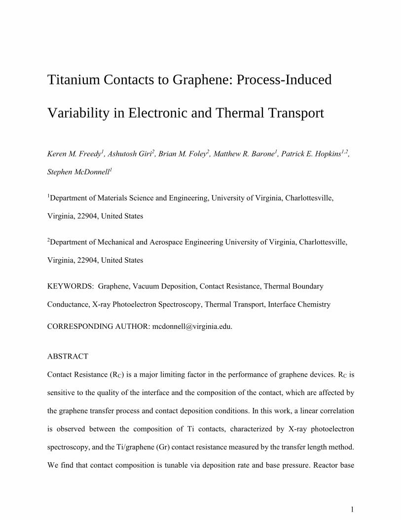
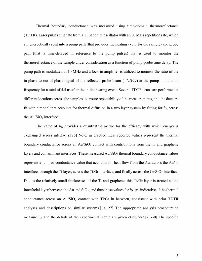
manifest in the electrical and thermal properties of the interface. Figure 1 shows oxide composition
vs. deposition rate for samples fabricated from three individually transferred pieces of graphene.
Figure 1. Plot of Ti oxide composition vs. deposition rate at a pressure of 1x10⁻⁷ Torr on
Gr/SiO2 samples. Each identical marker shape represents samples cut from the same piece of
graphene.

7
Each color represents a single piece of graphene transferred to SiO2 and subsequently split
into three (or four) samples to receive metal deposition at three (or four) different deposition rates.
Sample-to-sample variability is observed, but there appears to be a trend of decreasing oxide
composition with increasing deposition rate. The deposition rate determines the impingement rate
of Ti atoms on the surface of the substrate relative to the impingement rate of the oxidizing species
from residual gases. It is therefore expected that higher deposition rates result in lower oxide
composition, since at higher deposition rates, Ti atoms arrive at the sample surface at faster rates
than oxidizing species in the chamber. Anomalous data points can be explained by the presence of
additional oxidizing species from PMMA residues which will be addressed in the Discussion
section.
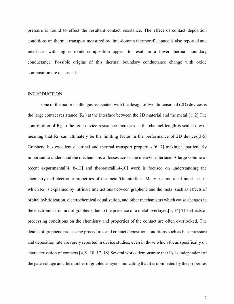
Base pressure also has a substantial effect which can dominate over deposition rate. The
base pressure is a measure of the quantity of residual gases in the chamber. Depositing at higher
pressures increases the amount of oxidizing species available for reaction with Ti, and depositing
at lower deposition rates increases the fraction of Ti atoms which will react with oxidizing species
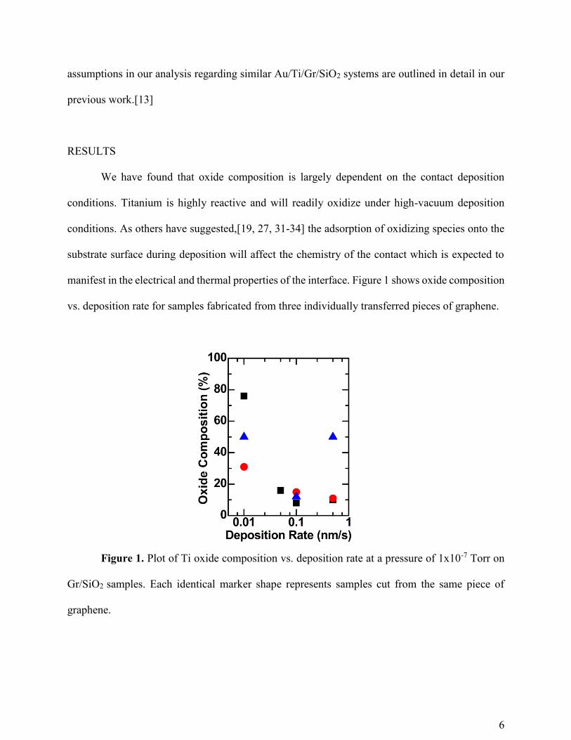
upon reaching the surface. This is observed in Figure 2. To overcome the issue of sample-to-
sample variability, each sample represented in Figure 2 was cut from a single piece Gr/SiO2
produced in a single transfer. Two out of the three samples were deposited on at the same rate and
different base pressures, and two out of three were deposited on at the same base pressure but
different rates. In Figure 2(a), (i) corresponds to a deposition 1x10⁻⁷ Torr and a rate of 0.01 nm/s,
(ii) corresponds to a deposition at 1x10⁻⁷ Torr and a rate of 0.1 nm/s and (iii) corresponds to a
pressure girof 1x10⁻⁶ Torr at a rate of 0.1 nm/s. The corresponding TLM data for each are shown
in Figure 2(b). The results indicate that base pressure has a stronger effect on contact composition
than deposition rate, since (iii) shows a comparable oxide composition of 78% compared with (i)
8
which is 67% and yet shows markedly different RC. It is known that UHV depositions result in
cleaner interfaces and improved RC for unreactive metals like Au.[3] Our comparison of samples
processed under lower and higher base pressures show that RC might be dominated by the
composition of the interface rather than the composition of the contact itself, as contacts with
similar oxide compositions ((i) and (iii)) exhibit a large difference in RC. The larger error bars and
confidence interval in the TLM data for (iii) are also indicative of greater variability in measured
RC throughout different regions of the sample. Comparison of spectra (i) and (ii) in Figure 2
illustrate the results reported in Figure 1 concerning the effect of deposition rate at a constant base
pressure.
Figure 2. (a) Ti 2p core-level spectra for Ti deposited onto samples cut from a single
Gr/SiO2 sample at different deposition conditions resulting in different oxide compositions. (b)
Corresponding TLM results for each sample where black line represents the linear fit and the red
lines represent the upper and lower 95% confidence bounds
9
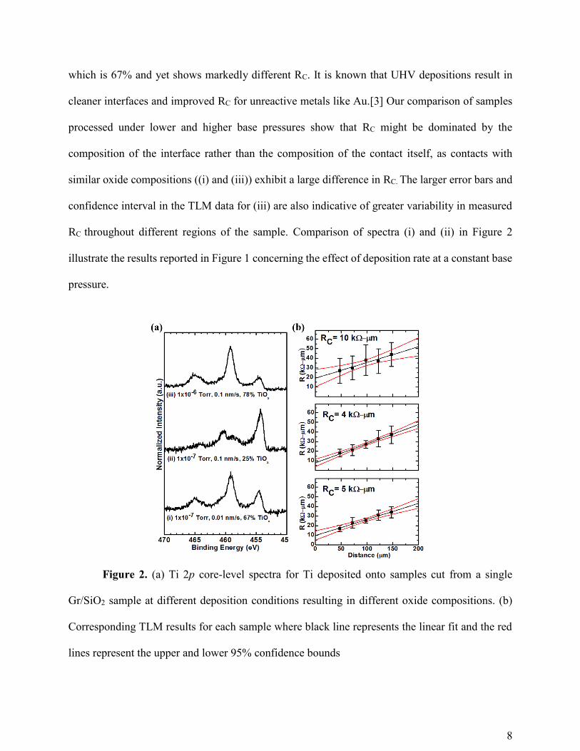
We have observed an overall correlation between the oxide composition of the contacts
shown in Figure 3.While large sample-to-sample variability is observed, the data has a linear
correlation coefficient of 0.7. The linear correlation coefficient describes the extent to which two
variables support a linear relation.[35] Thus, a value of this linear correlation coefficient close to
approaching unity indicates a linear relationship likely exists where the probability of correlation
depends on the number of data points acquired. For the thirteen values reported in this work, the
probability of a linear correlation is 99.2%. Thus we conclude there exists a linear relationship
between oxide composition and RC. Differences in the cleanliness of the interface observed in
Figure 2 might also explain why contacts of similar oxide composition show large variation in RC
as seen in Figure 3.
Figure 3. Plot of width-normalized contact resistivity as a function of oxide composition
showing a linear trend with a correlation coefficient of 0.7. Each set of identical markers on the
plot corresponds to samples which were cut from the same piece of transferred graphene but
processed under different conditions
10
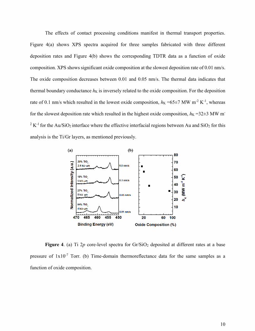
The effects of contact processing conditions manifest in thermal transport properties.
Figure 4(a) shows XPS spectra acquired for three samples fabricated with three different
deposition rates and Figure 4(b) shows the corresponding TDTR data as a function of oxide
composition. XPS shows significant oxide composition at the slowest deposition rate of 0.01 nm/s.
The oxide composition decreases between 0.01 and 0.05 nm/s. The thermal data indicates that
thermal boundary conductance hK is inversely related to the oxide composition. For the deposition
rate of 0.1 nm/s which resulted in the lowest oxide composition, hK =65±7 MW m-2 K-1, whereas
for the slowest deposition rate which resulted in the highest oxide composition, hK =32±3 MW m-
2 K-1 for the Au/SiO2 interface where the effective interfacial regions between Au and SiO2 for this
analysis is the Ti/Gr layers, as mentioned previously.
Figure 4. (a) Ti 2p core-level spectra for Gr/SiO2 deposited at different rates at a base
pressure of 1x10⁻⁷ Torr. (b) Time-domain thermoreflectance data for the same samples as a
function of oxide composition.
11
The measured value of hK for the slower deposition rates matches very well with those
measured for a similar Au/Ti/Gr/SiO2 interface deposited at 0.05 nm/s and reported by Koh et
al.[27] The twofold increase in hK with the faster deposition rate corresponds to the relative
decrease in the oxide composition between the different deposition rates as shown in Figure 4(a).
Thus, a higher oxide composition in the Ti layer at an Au/Ti/Gr/SiO2 contact leads to a lower hK
(higher resistance) than a lower oxide composition. Stated differently, our results suggest that to
minimize the thermal resistance at an Au/Ti/Gr/SiO2 contact, the Ti should be as metallic as
possible. In contrast to thermal transport, electrical transport does not appear to be as sensitive to
the composition of the contact for this particular sample, however the results shown in Figure 3
indicate that the reactor base pressure does have an impact on RC.
DISCUSSION
It is apparent in Figure 1 that samples processed identically might result in different oxide
compositions. A major source of variability in the Gr/metal interface chemistry is related to
PMMA residue from the transfer process.[20, 36, 37] PMMA is typically removed by dissolution
in acetone followed by an anneal in UHV at a temperature high enough to dissociate the various
hydrocarbon species.[38] The thermal decomposition of PMMA is inherently a random process,
and generated radicals can react with defects in the graphene or form longer polymer chains that
cannot be removed.[39] Therefore, samples which undergo the same PMMA removal process can
be left with different quantities of PMMA residue, and the quantity of PMMA residue is unlikely
to be uniform across a single sample. Lee et al. have shown that a PMMA-free transfer process
results in lower contact resistance than that which uses PMMA.[40] PMMA residues are known
to dope graphene and alter its electronic properties.[38] Furthermore, transport across the Ti/Gr
12
interface will be inhibited by the presence of contaminants which scatter charge carriers and
obstruct hybridization between the graphene π-orbitals and Ti metal d-orbitals.[5, 14] Orbital
hybridization will be inhibited both by the presence of polymer residues at the interface and by the
presence of an oxidized contact rather than a metallic one. It has been shown that PMMA residues
react with Ti overlayers.[41] Other sources of variability in both the interface and contact
chemistry could be related to intrinsic defects in the CVD-grown graphene film or due to other
extrinsic effects of transfer process including residual Cu, incomplete removal of graphene from
the back of the Cu foil, wrinkles and tears in the film, or adsorbates. While measures can be taken
to assess the quality and uniformity of the transferred graphene prior to device fabrication, such as
characterization with Raman spectroscopy,[37, 38, 42] these defects are inherent to the transfer
process and are fundamentally uncontrollable.
Despite the inevitable sample-to-sample variability, our results suggest that some degree
of control over contact composition is achievable during the deposition process, particularly via
deposition rate and base pressure. The overall linear correlation between oxide composition and
RC summarized in Figure 3 is not surprising given that the electrical resistivity of TiO2 is orders
of magnitude higher than that of metallic Ti.[43] Since the contact resistance includes any
contribution to resistance that is independent of the channel length[9], resistances within the Au
and Ti layers, and at the Au/TiOx and graphene/TiOx interfaces are all contributors to the
measured value. The results presented in Figure 3 indicate that the cleanliness of the
graphene/TiOx interface likely dominates RC to a greater extent than the oxide composition.
The possible origins of the change in thermal boundary conductance with change in oxygen
content of the Ti layer between the Au and graphene could manifest from various changes in
electronic and vibrational scattering and interfacial transport in each layer of the Au/Ti/Gr/SiO2
13
boundary region. The major contributors to this change in thermal resistance, R = (1/hK) ~15.9
m2 K GW-1, could be the change in hK at the Au/Ti interface, the change in thermal conductivity
of the Ti, and the change in hK across the Ti/Gr/SiO2 interface that would occur with a change in
oxygen content in the Ti layer. In the extreme cases for thermal conductivity of the Ti layer, one
would expect the Ti layer to either be fully TiO2 or metallic Ti (clearly these are not the cases in
our study, but we pose these extreme cases for exemplary purposes). Assuming the extreme cases
of the thermal conductivity of amorphous TiO2 (~1.2 W m-1 K-1)[44] and that of crystalline metallic
Ti (~21.9 W m-1 K-1)[45], this leads to a change in resistance of this layer as R = 5x10⁻⁹/1.2 -
5x10⁻⁹/21.9 ~ 4 m2 K GW-1. We note this example calculation considers the extreme case to
calculate the maximum hypothetical resistance change of this layer. As is evident, the above
calculation for R cannot explain the entire observed change in thermal boundary resistance with
different oxygen content in the Ti layer (as previously mentioned, R ~15.9 m2 K GW-1). We note
also that size effects were not considered in this R calculation.[46-48] Thus, the change in thermal
resistance of the Ti layer cannot solely explain measured change in thermal boundary conductance.
Another possibility for the observed change in thermal conductance across the
Au/Ti/Gr/SiO2 region is the change in the Ti/Gr/SiO2 thermal boundary conductance. Our previous
work has demonstrated that changes in graphene surface chemistry induced from plasma
functionalization (including oxygen functionalization) can lead to appreciable changes in thermal
boundary conductance.[13, 49, 50] Thus, one could hypothesize that the change in oxygen
stoichiometry in the Ti layer would also lead to changes in how the Ti reacts with residues and
thereby lead to changes in the chemistry at the Ti/Gr interface; thus impacting thermal boundary
conductance. We note that residual PMMA residue is present on all samples. Therefore it is
presumed that all Gr/Ti interfaces will actually be TiOx/Gr with some variation in amount of
14
hydrocarbon incorporated.[41] At this time the impact of the variations in hydrocarbon
incorporation at the interface on the thermal boundary conductance is unknown. Therefore, we
cannot rule this out as a potential mechanism, and thus leave an intricate study of the chemistry
effects on Ti/Gr thermal boundary conductance to future work.
Finally, we consider the change in thermal boundary conductance at the Au/Ti interface as
a possible contributor to the measured change in R of the Au/Ti/Gr/SiO2 interfacial region. At
pure metal/metal interfaces, the thermal boundary conductance is driven by the electron densities
of states at the Fermi energies of the metals[51-54], and this corresponding thermal boundary
conductance can be more than an order of magnitude greater than those at metal/non-metal
interfaces.[55] While the thermal boundary conductances across Au/metal Ti and Au/TiO2
interfaces have not been explicitly and reliably measured previously due to the exceptionally high
hK affiliated with metal/metal interfaces, we can assume that the resistance associated with the
metallic phase of Ti in contact with the Au will offer negligible resistance as compared to the non-
metal oxide phases in the Ti layer. Indeed, typical values for thermal boundary conductances across
Au/non-metal interfaces range from ~50 – 100 MW m-2 K-1, [53, 56-58] limited by the relatively
narrow spectral phonon bandwidth in the Au. This corresponds to a R of ~10 – 20 m2 K GW-1,
on the order of our measured change in thermal boundary conductance with changes in oxygen
content in the Ti (R ~15.9 m2 K GW-1).
We estimate these various electron-electron and phonon-phonon resistances at the Au/Ti
layer interface in more quantitative detail through the use of diffuse mismatch models (DMM). As
mentioned previously, the electron DMM (eDMM) predicts the thermal boundary conductance
between two materials with large electron densities of states compared to phonon density of states
(e.g., at metal/metal interfaces).[51, 53, 54] Assuming values for the electron density of states at
15
the Fermi energy and calculated Fermi velocities for Au and Ti[59, 60], we predict a thermal
boundary resistance of Ree,Au/Ti = 0.17 m2 K GW-1 (thermal boundary conductance of 5,970 MW
m-2 K-1 between the electronic systems in Au and Ti, assuming both are pure metals). This eDMM
calculation thus predicts the thermal transport across the Au/Ti interface in the case when Ti is
fully metallic. When the Ti layer is oxidized, this electron-electron interfacial thermal transport
pathway will be reduced, and thus the Au phonon/Ti phonon interfacial thermal transport pathway
can become a dominant conductance, since the electronic densities of states of the TiOx regions of
the adhesion layer will be greatly reduced compared to the metallic Ti regions. Thus, we quantify
this phonon-phonon thermal boundary resistance using the traditionally implemented phonon
DMM (pDMM).[26] We calculate the phonon-phonon thermal boundary resistance of two cases:
Au/Ti and Au/TiO2 (rutile). In our pDMM calculations, we assume sine-type phonon dispersions
of the longitudinal and two degenerate transverse acoustic modes in each material with zone edge
phonon frequencies taken from Ref. [61] for Au (X direction), Ref. [62] for Ti (A
direction), and Ref. [63] for rutile (A direction). From this, we predict phonon-phonon thermal
boundary resistances of Rpp,Au/Ti = 6.17 m2 K GW-1 (hK,pp,Au/Ti = 162 MW m-2 K-1) and Rpp,Au/TiO2 =
6.76 m2 K GW-1 (hK,pp,Au/TiO2 = 148 MW m-2 K-1) for the Au/Ti and Au/TiO2, respectively. Based
on these eDMM and pDMM calculations, the predicted change in thermal boundary resistance
associated with the change from a metal/metal Au/Ti interface (electron-electron) to a metal/non-
metal Au/Ti (Au/TiO2) interface (phonon-phonon) as R = 6.0 m2 K GW-1 (6.6 m2 K GW-1). While
this calculation of R is slightly lower than our observed change in thermal boundary resistance
across the Au/Ti/Gr/SiO2 interfaces (R ~15.9 m2 K GW-1), we caution that the assumptions
required for DMM predictions could lead to uncertainties in these predicted values. Regardless, a
16
clear change in Au/Ti thermal boundary conductance will occur when the interfacial transport
transitions from an electron to phonon dominated process.
These simple qualitative and quantitative analyses suggest that the changes in thermal
boundary conductance across the Au/Ti/Gr/SiO2 boundary originate from changes in resistance at
the Au/Ti interface and possible additional changes in thermal conductivity in the Ti layer.
However, much more work needs to be pursued to study this precise interface in more detail and
to understand the fundamental electron and phonon scattering mechanisms driving this thermal
transport process with respect to changes in oxygen chemistry. This points to the future promise
of manipulating metal/metal contacts through metal type and chemistry to impact the thermal
resistances of graphene devices.
CONCLUSION
This work sheds light on the inherent variability in graphene devices. By attempting to
correlate deposition conditions with the contact composition and contact resistance, we have found
that contact resistance is sensitive to the partial pressure during contact deposition, and that the
oxide of a Ti contact can strongly impact the thermal boundary conductance. It should be noted
that reactor pressure and deposition rate are not parameters that are typically reported when
describing device fabrication and yet this work demonstrates that both clearly affect device
properties. The relationship between interface chemistry and contact resistance as well as thermal
transport opens doors for interface engineering. While the role of interface morphology has not
been explored in this study, we intend to examine it in future work.
17
ACKNOWLEDGMENTS
This work was supported in part by the Army Research Office, Grant No. W911NF-16-1-0320.
The Authors thank Prof. Suzanne Mohney for useful discussions. They also thank Genevieve
Glista for her work on optimization of the graphene transfer process.
REFERENCES
[1] Allain A, Kang J, Banerjee K and Kis A 2015 Electrical contacts to two-dimensional
semiconductors Nat Mater 14 1195-205
[2] Xu Y, Cheng C, Du S, Yang J, Yu B, Luo J, Yin W, Li E, Dong S, Ye P and Duan X
2016 Contacts between Two- and Three-Dimensional Materials: Ohmic, Schottky, and p–
n Heterojunctions ACS Nano 10 4895-919
[3] English C D, Shine G, Dorgan V E, Saraswat K C and Pop E 2016 Improved Contacts to
MoS2 Transistors by Ultra-High Vacuum Metal Deposition Nano. Lett. 16 3824-30
[4] Politou M, Asselberghs I, Radu I, Conard T, Richard O, Lee C S, Martens K, Sayan S,
Huyghebaert C, Tokei Z, De Gendt S and Heyns M 2015 Transition metal contacts to
graphene Appl. Phys. Lett. 107 153104
[5] Toriumi A and Nagashio K 2016 Metal Contacts to Graphene 2D Materials for
Nanoelectronics 17 53
[6] Tian L, Anilkumar P, Cao L, Kong C Y, Meziani M J, Qian H, Veca L M, Thorne T J,
Tackett K N, Edwards T and Sun Y-P 2011 Graphene Oxides Dispersing and Hosting
Graphene Sheets for Unique Nanocomposite Materials ACS Nano 5 3052-8
[7] Hou Z-L, Song W-L, Wang P, Meziani M J, Kong C Y, Anderson A, Maimaiti H,
LeCroy G E, Qian H and Sun Y-P 2014 Flexible Graphene–Graphene Composites of
Superior Thermal and Electrical Transport Properties ACS Appl. Mater. Interfaces 6
15026-32
[8] Gong C, McDonnell S, Qin X, Azcatl A, Dong H, Chabal Y J, Cho K and Wallace R M
2014 Realistic Metal–Graphene Contact Structures ACS Nano 8 642-9
[9] Venugopal A, Colombo L and Vogel E M 2010 Contact resistance in few and multilayer
graphene devices Appl. Phys. Lett. 96 013512
[10] Xia F, Perebeinos V, Lin Y-m, Wu Y and Avouris P 2011 The origins and limits of
metal-graphene junction resistance Nat Nano 6 179-84
[11] Nagashio K, Nishimura T, Kita K and Toriumi A 2009 Metal/graphene contact as a
performance Killer of ultra-high mobility graphene analysis of intrinsic mobility and
contact resistance. In: IEEE Int. Electron Devices Meet., pp 1-4
[12] Nagashio K, Nishimura T, Kita K and Toriumi A 2010 Contact resistivity and current
flow path at metal/graphene contact Appl. Phys. Lett. 97 143514
[13] Foley B M, Hernández S C, Duda J C, Robinson J T, Walton S G and Hopkins P E 2015
Modifying Surface Energy of Graphene via Plasma-Based Chemical Functionalization to
Tune Thermal and Electrical Transport at Metal Interfaces Nano. Lett. 15 4876-82
18
[14] Gong C, Lee G, Shan B, Vogel E M, Wallace R M and Cho K 2010 First-principles study
of metal–graphene interfaces J. Appl. Phys. 108 123711
[15] Kang J, Sarkar D, Liu W, Jena D and Banerjee K 2012 A computational study of metal-
contacts to beyond-graphene 2D semiconductor materials. In: Int. Electron Devices
Meet., pp 17.4.1-.4.4
[16] Ran Q, Gao M, Guan X, Wang Y and Yu Z 2009 First-principles investigation on
bonding formation and electronic structure of metal-graphene contacts Appl. Phys. Lett.
94 103511
[17] Nouchi R, Saito T and Tanigaki K 2012 Observation of negative contact resistances in
graphene field-effect transistors J. Appl. Phys. 111 084314
[18] Blake P, Yang R, Morozov S V, Schedin F, Ponomarenko L A, Zhukov A A, Nair R R,
Grigorieva I V, Novoselov K S and Geim A K 2009 Influence of metal contacts and
charge inhomogeneity on transport properties of graphene near the neutrality point Solid
State Commun. 149 1068-71
[19] Russo S, Craciun M F, Yamamoto M, Morpurgo A F and Tarucha S 2010 Contact
resistance in graphene-based devices Phys. E 42 677-9
[20] Reina A, Son H, Jiao L, Fan B, Dresselhaus M S, Liu Z and Kong J 2008 Transferring
and Identification of Single- and Few-Layer Graphene on Arbitrary Substrates J. Phys.
Chem. C 112 17741-4
[21] Suk J W, Kitt A, Magnuson C W, Hao Y, Ahmed S, An J, Swan A K, Goldberg B B and
Ruoff R S 2011 Transfer of CVD-Grown Monolayer Graphene onto Arbitrary Substrates
ACS Nano 5 6916-24
[22] Freedy K M, Litwin P M and McDonnell S J 2017 (Invited) In-Vacuo Studies of
Transition Metal Dichalcogenide Synthesis and Layered Material Integration ECS
Transactions 77 11-25
[23] http://kolxpd.kolibrik.net.
[24] Gahoi A, Wagner S, Bablich A, Kataria S, Passi V and Lemme M C 2016 Contact
resistance study of various metal electrodes with CVD graphene Solid-State Electronics
125 234-9
[25] Moon J S, Antcliffe M, Seo H C, Curtis D, Lin S, Schmitz A, Milosavljevic I, Kiselev A
A, Ross R S, Gaskill D K, Campbell P M, Fitch R C, Lee K M and Asbeck P 2012 Ultra-
low resistance ohmic contacts in graphene field effect transistors Appl. Phys. Lett. 100
203512
[26] Swartz E T and Pohl R O 1989 Thermal boundary resistance Reviews of Modern Physics
61 605-68
[27] Koh Y K, Bae M-H, Cahill D G and Pop E 2010 Heat Conduction across Monolayer and
Few-Layer Graphenes Nano. Lett. 10 4363-8
[28] Cahill D G 2004 Analysis of heat flow in layered structures for time-domain
thermoreflectance Rev. Sci. Instrum. 75 5119-22
[29] Schmidt A J, Chen X and Chen G 2008 Pulse accumulation, radial heat conduction, and
anisotropic thermal conductivity in pump-probe transient thermoreflectance Rev. Sci.
Instrum. 79 114902
[30] Hopkins P E, Serrano J R, Phinney L M, Kearney S P, Grasser T W and Harris C T 2010
Criteria for Cross-Plane Dominated Thermal Transport in Multilayer Thin Film Systems
During Modulated Laser Heating J. Heat Transfer 132 081302-
19
[31] McCreery R, Dieringer J, Solak A O, Snyder B, Nowak A M, McGovern W R and
DuVall S 2004 Molecular Rectification and Conductance Switching in Carbon-Based
Molecular Junctions by Structural Rearrangement Accompanying Electron Injection [J.
Am. Chem. Soc. 2003, 125, 10748−10758]. J. Am. Chem. Soc. 126 6200-
[32] McGovern W R, Anariba F and McCreery R L 2005 Importance of oxides in
carbon/molecule/metal molecular junctions with titanium and copper top contacts J.
Electrochem. Soc. 152 E176-E83
[33] McDonnell S, Smyth C, Hinkle C L and Wallace R M 2016 MoS2–Titanium Contact
Interface Reactions ACS Appl. Mater. Interfaces 8 8289-94
[34] Felten A, Suarez-Martinez I, Ke X, Van Tendeloo G, Ghijsen J, Pireaux J-J, Drube W,
Bittencourt C and Ewels C P 2009 The Role of Oxygen at the Interface between Titanium
and Carbon Nanotubes ChemPhysChem 10 1799-804
[35] Taylor J R 1997 Introduction To Error Analysis: The Study of Uncertainties in Physical
Measurements: University Science Books)
[36] Li X, Zhu Y, Cai W, Borysiak M, Han B, Chen D, Piner R D, Colombo L and Ruoff R S
2009 Transfer of Large-Area Graphene Films for High-Performance Transparent
Conductive Electrodes Nano. Lett. 9 4359-63
[37] Chan J, Venugopal A, Pirkle A, McDonnell S, Hinojos D, Magnuson C W, Ruoff R S,
Colombo L, Wallace R M and Vogel E M 2012 Reducing Extrinsic Performance-
Limiting Factors in Graphene Grown by Chemical Vapor Deposition ACS Nano 6 3224-9
[38] Pirkle A, Chan J, Venugopal A, Hinojos D, Magnuson C W, McDonnell S, Colombo L,
Vogel E M, Ruoff R S and Wallace R M 2011 The effect of chemical residues on the
physical and electrical properties of chemical vapor deposited graphene transferred to
SiO2 Appl. Phys. Lett. 99 122108
[39] Lin Y C, Lu C C, Yeh C H, Jin C, Suenaga K and Chiu P W 2012 Graphene annealing:
how clean can it be? Nano. Lett. 12 414-9
[40] Lee J e a 2013 Clean transfer of graphene and its effect on contact resistance Appl. Phys.
Lett. 103 103104
[41] Joiner C A, Roy T, Hesabi Z R, Chakrabarti B and Vogel E M 2014 Cleaning graphene
with a titanium sacrificial layer Appl. Phys. Lett. 104 223109
[42] Gong C, Floresca H C, Hinojos D, McDonnell S, Qin X, Hao Y, Jandhyala S, Mordi G,
Kim J, Colombo L, Ruoff R S, Kim M J, Cho K, Wallace R M and Chabal Y J 2013
Rapid Selective Etching of PMMA Residues from Transferred Graphene by Carbon
Dioxide J. Phys. Chem. C 117 23000-8
[43] Haynes W M 2011 CRC Handbook of Chemistry and Physics, 92nd Edition: CRC Press)
[44] Hopkins P E, Mittal M, Phinney L M, Grillet A M and Furst E M 2011 Ultra-low thermal
conductivity of ellipsoidal TiO2 nanoparticle films Appl. Phys. Lett. 99 133106
[45] Lide D R 2008 CRC Handbook for Chemistry and Physics, 89th edition
[46] Chen G 2005 Nanoscale Energy Transport and Conversion: A Parallel Treatment of
Electrons, Molecules, Phonons, and Photons: Oxford University Press)
[47] Stewart D and Norris P M 2000 Size effects on the thermal conductivity of thin metallic
wires: microscale implications Microscale Thermophys. Eng. 4 89-101
[48] Tellier C R, Tosser A J and Siddall G 2016 Size Effects in Thin Films: Elsevier Science)
[49] Hopkins P E, Baraket M, Barnat E V, Beechem T E, Kearney S P, Duda J C, Robinson J
T and Walton S G 2012 Manipulating Thermal Conductance at Metal–Graphene Contacts
via Chemical Functionalization Nano. Lett. 12 590-5
20
[50] Walton S G, Foley B M, Hernández S C, Boris D R, Baraket M, Duda J C, Robinson J T
and Hopkins P E 2017 Plasma-based chemical functionalization of graphene to control
the thermal transport at graphene-metal interfaces Surf. Coat. Technol. 314 148-54
[51] Hopkins P E, Beechem T E, Duda J C, Smoyer J L and Norris P M 2010 Effects of
subconduction band excitations on thermal conductance at metal-metal interfaces Appl.
Phys. Lett. 96 011907
[52] Giri A, Gaskins J T, Donovan B F, Szwejkowski C, Warzoha R J, Rodriguez M A,
Ihlefeld J and Hopkins P E 2015 Mechanisms of nonequilibrium electron-phonon
coupling and thermal conductance at interfaces J. Appl. Phys. 117 105105
[53] Cheaito R, Hattar K, Gaskins J T, Yadav A K, Duda J C, Beechem T E, Ihlefeld J F,
Piekos E S, Baldwin J K and Misra A 2015 Thermal flux limited electron Kapitza
conductance in copper-niobium multilayers Appl. Phys. Lett. 106 093114
[54] Gundrum B C, Cahill D G and Averback R S 2005 Thermal conductance of metal-metal
interfaces Phys. Rev. B 72 245426
[55] Hopkins P E 2013 Thermal transport across solid interfaces with nanoscale
imperfections: effects of roughness, disorder, dislocations, and bonding on thermal
boundary conductance ISRN Mech. Eng. 2013
[56] Duda J C, Yang C Y P, Foley B M, Cheaito R, Medlin D L, Jones R E and Hopkins P E
2013 Influence of interfacial properties on thermal transport at gold:silicon contacts Appl.
Phys. Lett. 102 081902
[57] Oh D W, Kim S, Rogers J A, Cahill D G and Sinha S 2011 Interfacial Thermal
Conductance of Transfer‐Printed Metal Films Adv. Mater. 23 5028-33
[58] Donovan B F, Szwejkowski C J, Duda J C, Cheaito R, Gaskins J T, Peter Yang C Y,
Constantin C, Jones R E and Hopkins P E 2014 Thermal boundary conductance across
metal-gallium nitride interfaces from 80 to 450 K Appl. Phys. Lett. 105 203502
[59] Lin Z, Zhigilei L V and Celli V 2008 Electron-phonon coupling and electron heat
capacity of metals under conditions of strong electron-phonon nonequilibrium Phys. Rev.
B 77 075133
[60] Jafari M, Jahandoost A, Vaezzadeh M and Zarifi N 2011 Effect of pressure on the
electronic structure of hcp Titanium arXiv preprint arXiv:1107.3948
[61] Lynn J, Smith H and Nicklow R 1973 Lattice dynamics of gold Phys. Rev. B 8 3493
[62] Stassis C, Arch D, Harmon B and Wakabayashi N 1979 Lattice dynamics of hcp Ti Phys.
Rev. B 19 181
[63] Mei Z-G, Wang Y, Shang S-L and Liu Z-K 2011 First-principles study of lattice
dynamics and thermodynamics of TiO2 polymorphs Inorg. Chem. 50 6996-7003
21
SUPPORTING INFORMATION
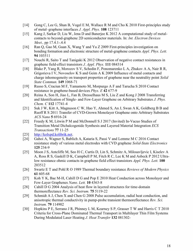
Compositional Analysis
X-ray photoelectron spectroscopy of the Ti 2p core level was used to quantify the composition of
oxide and metal components. The spectra were fit using kolXPD software.[23] An example fit is
shown in Figure S1 where the metal peaks are fit with a Doniach-Sunjic lineshape convoluted with
a Gaussian, and the oxide peaks are fit with a Voigt lineshape. The integrated areas, or amplitudes,
of the 2p core level peaks corresponding to metal (𝐼𝑚𝑒𝑡𝑎𝑙) and oxide (𝐼𝑜𝑥𝑖𝑑𝑒) are used to calculate
% oxide as follows:
% 𝑜𝑥𝑖𝑑𝑒 =𝐼𝑜𝑥𝑖𝑑𝑒
𝐼𝑜𝑥𝑖𝑑𝑒 + 𝐼𝑚𝑒𝑡𝑎𝑙× 100
Figure S1. Example of peak deconvolution of a Ti 2p spectrum for Ti deposited on Gr/SiO2
(base pressure 1x10⁻⁷ Torr, 0.01 nm/s deposition rate for this particular sample)
22
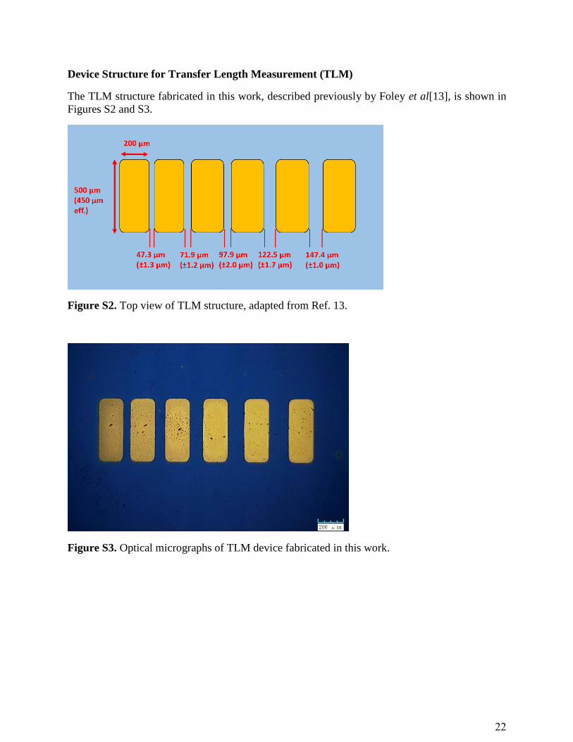
Device Structure for Transfer Length Measurement (TLM)
The TLM structure fabricated in this work, described previously by Foley et al[13], is shown in
Figures S2 and S3.
Figure S2. Top view of TLM structure, adapted from Ref. 13.
Figure S3. Optical micrographs of TLM device fabricated in this work.

23
Coefficient of Linear Correlation for RC vs. Oxide Composition
The extent which there exists a linear correlation between a set of points (x1,y1)…(xN,yN) is
measured by the linear correlation coefficient, r, given by[35]
𝑟 =𝜎𝑥𝑦
𝜎𝑥𝜎𝑦 (Eq. 1)
where 𝜎𝑥𝑦 is the covariance, and 𝜎𝑥 and 𝜎𝑦 are the standard deviations of x and y. Eq. 1 can then
be written as
𝑟 =∑(𝑥𝑖−�̅�)(𝑦𝑖−�̅�)
√∑(𝑥𝑖−�̅�)2 ∑(𝑦𝑖−�̅�)2 (Eq. 2)
If all points (xi,yi) lie exactly on the line 𝑦𝑖 = 𝐴 + 𝐵𝑥 then the value of r will be ±1. The
quantitative significance of r depends on the number of measurements, N, which determines the
probability that two uncorrelated variables will yield a particular value of r. This can be applied
conversely to determine the probability that a particular value of r indicates that two variables are
correlated. For the data reported in this work plotted in Figure 1 of the text, the measurement of
oxide composition and RC on thirteen distinct samples yielded a correlation coefficient of 0.7. By
the methods reported in Ref. 1, this represents a 0.8% probability that oxide composition and RC
are uncorrelated. We therefore infer a 99.2% probability that RC is linearly correlated with oxide
composition. This value corresponds to a highly significant probability of linear correlation.
24
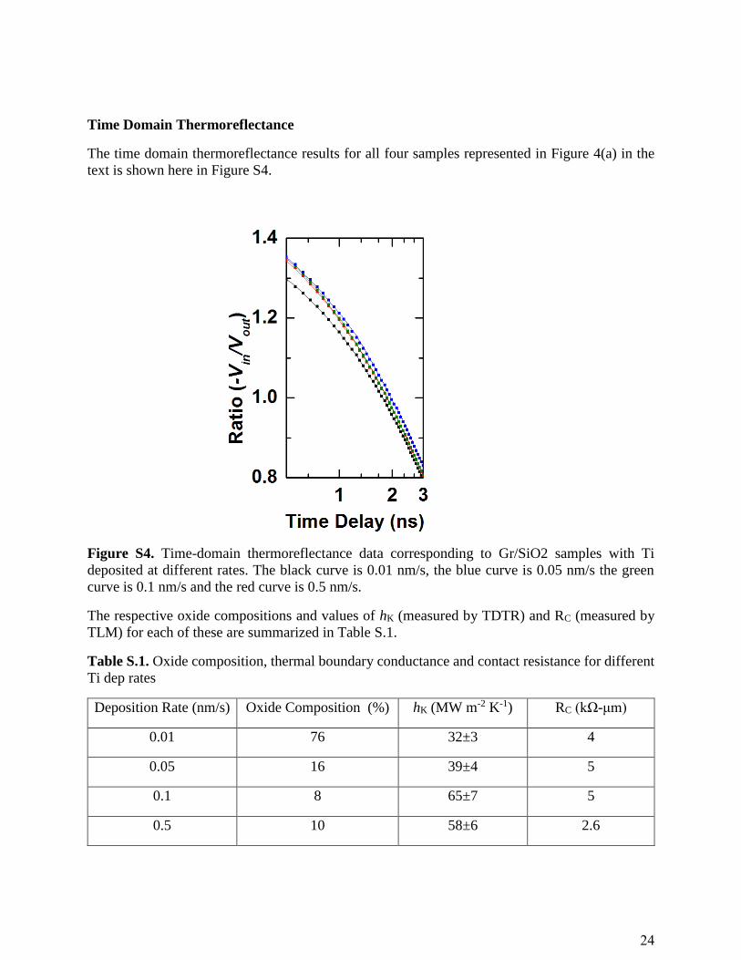
Time Domain Thermoreflectance
The time domain thermoreflectance results for all four samples represented in Figure 4(a) in the
text is shown here in Figure S4.
Figure S4. Time-domain thermoreflectance data corresponding to Gr/SiO2 samples with Ti
deposited at different rates. The black curve is 0.01 nm/s, the blue curve is 0.05 nm/s the green
curve is 0.1 nm/s and the red curve is 0.5 nm/s.
The respective oxide compositions and values of hK (measured by TDTR) and RC (measured by
TLM) for each of these are summarized in Table S.1.
Table S.1. Oxide composition, thermal boundary conductance and contact resistance for different
Ti dep rates
Deposition Rate (nm/s) Oxide Composition (%) hK (MW m-2 K-1) RC (kΩ-μm)
0.01 76 32±3 4
0.05 16 39±4 5
0.1 8 65±7 5
0.5 10 58±6 2.6