plasmonic terahertz lasing in an array of graphene nanocavities
TRANSCRIPT
PHYSICAL REVIEW B 86, 195437 (2012)
Plasmonic terahertz lasing in an array of graphene nanocavities
V. V. Popov,1,2,* O. V. Polischuk,1,2 A. R. Davoyan,1 V. Ryzhii,3 T. Otsuji,3 and M. S. Shur4
1Kotelnikov Institute of Radio Engineering and Electronics (Saratov Branch), Russian Academy of Sciences, Saratov 410019, Russia2Saratov State University, Saratov 410012, Russia
3Research Institute for Electrical Communication, Tohoku University, Sendai 980-8577, Japan4Department of Electrical, Computer, and Systems Engineering, Rensselaer Polytechnic Institute, Troy, New York 12180, USA
(Received 27 July 2012; revised manuscript received 31 October 2012; published 30 November 2012)
We propose a novel concept of terahertz lasing based on stimulated generation of plasmons in a planararray of graphene resonant micro/nanocavities strongly coupled to terahertz radiation. Due to the strongplasmon confinement and superradiant nature of terahertz emission by the array of plasmonic nanocavities, theamplification of terahertz waves is enhanced by many orders of magnitude at the plasmon resonance frequencies.We show that the lasing regime is ensured by the balance between the plasmon gain and plasmon radiativedamping.
DOI: 10.1103/PhysRevB.86.195437 PACS number(s): 73.20.Mf, 07.57.Hm, 78.67.Wj, 42.60.Lh
Fundamental limits reached by the available sources of elec-tromagnetic radiation based on classical electronic oscillationsradiating at radio and microwave frequencies, and on electrontransitions between quantized energy levels corresponding toinfrared and optical frequencies, give rise to the so-calledterahertz (THz) gap.1,2
Extraordinary electronic properties of novel materialsmight help to go beyond the limits of the THz gap. In particular,graphene, a two-dimensional monolayer of graphite, hasreceived a great deal of interest recently due to its uniqueelectronic properties stemming from a linear (Dirac-type)gapless carrier energy spectrum E = ±VF |p| (see the insetin Fig. 1), where E and p are the electron (hole) energy andmomentum, respectively, VF ≈ 108 cm/s is the Fermi velocity,which is a constant for graphene, and upper and lower signsrefer to the conduction and valence bands, respectively.3,4
Graphene is especially promising for THz photonics5 due toits zero (or small in doped graphene) band gap.
Interband population inversion in graphene can be achievedby its optical pumping6 or carrier injection.7 At sufficientlystrong excitation, the interband stimulated emission of photonscan prevail over the intraband (Drude) absorption. In this case,the real part of the dynamic conductivity of graphene canbe negative in the THz range. This effect can be used forTHz photon lasing.8 Stimulated emission of near-infrared9
and THz10 photons from population inverted graphene wasrecently observed.
Graphene exhibits strong plasmonic response due to bothhigh density and small “relativistic” effective mass mF =EF /V 2
F of free carriers, where EF is the Fermi energy. Disper-sion of the plasma waves (plasmons) in graphene was studiedfor intrinsic (undoped)11,12 and doped (or gated)13–17 graphene.Plasmon resonances in graphene can be controlled in graphenenanoribbon arrays18–20 and tuned in the entire THz range,depending on the direction of the plasmon propagation in thearray plane and/or by varying the nanoribbon width. Plasmonsin patterned graphene strongly couple to electromagneticwaves, which makes graphene nanostructures very promisingfor the development of tunable graphene-based THz plasmonicmetamaterials.19,21–24
Compared with the stimulated emission of electromagneticmodes (photons), the stimulated emission of plasmons by the
interband transitions in population inverted graphene exhibits amuch higher gain due to a small group velocity of the plasmonsin graphene and strong confinement of the plasmon fieldin the vicinity of the graphene layer.25,26 Plasmon emissiondue to recombination of the electron-hole pairs in graphenewas demonstrated experimentally recently.27 However, a largeplasmon gain in graphene leads to strong dephasing of theplasmon mode, hence preventing THz lasing. Also, strongcoupling between the plasmons in graphene and electromag-netic radiation can hinder THz lasing from nonequilibriumplasmons. Therefore, to the best of our knowledge, neitherplasmonic amplification of THz radiation nor THz plasmoniclasing in graphene has been reported so far.
In this paper, we consider the amplification of a THz waveby the stimulated generation of resonant plasmons in a planarperiodic array of graphene plasmonic micro/nanocavitiesstrongly coupled to THz radiation. We show that, due to thestrong confinement of the plasmon modes in the graphenemicro/nanocavities and superradiant nature of electromagneticemission from the array of the plasmonic micro/nanocavities,the amplification of THz waves is enhanced by several ordersof magnitude at the plasmon resonance frequencies. It isshown that the plasmonic THz lasing becomes possible due torestoring the plasmon coherence in the graphene nanocavitiesstrongly coupled to THz radiation at the balance between theplasmon gain and plasmon radiative damping.
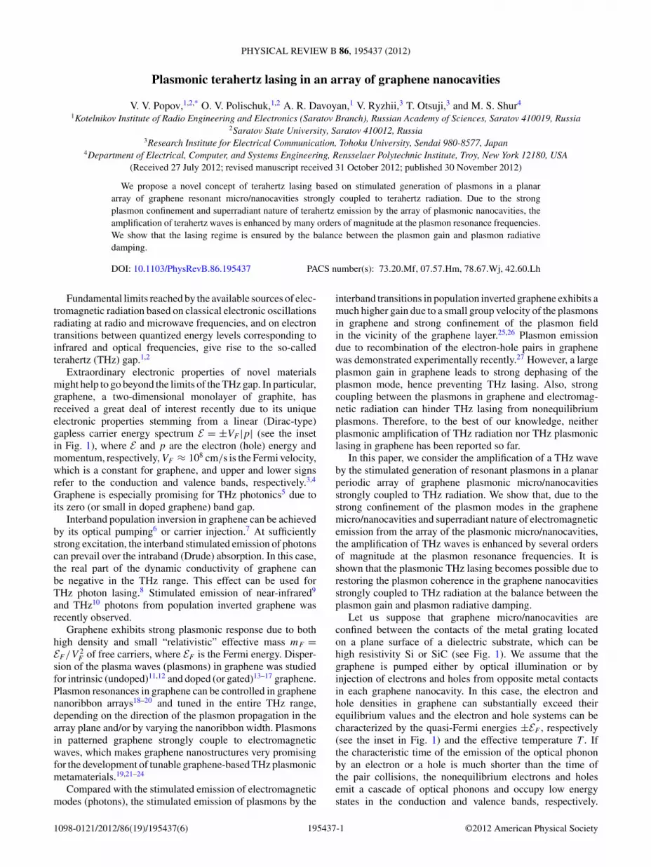
Let us suppose that graphene micro/nanocavities areconfined between the contacts of the metal grating locatedon a plane surface of a dielectric substrate, which can behigh resistivity Si or SiC (see Fig. 1). We assume that thegraphene is pumped either by optical illumination or byinjection of electrons and holes from opposite metal contactsin each graphene nanocavity. In this case, the electron andhole densities in graphene can substantially exceed theirequilibrium values and the electron and hole systems can becharacterized by the quasi-Fermi energies ±EF , respectively(see the inset in Fig. 1) and the effective temperature T . Ifthe characteristic time of the emission of the optical phononby an electron or a hole is much shorter than the time ofthe pair collisions, the nonequilibrium electrons and holesemit a cascade of optical phonons and occupy low energystates in the conduction and valence bands, respectively.
195437-11098-0121/2012/86(19)/195437(6) ©2012 American Physical Society

V. V. POPOV et al. PHYSICAL REVIEW B 86, 195437 (2012)
L
a
THz Output
E(s-e)
Pump
THz Input
graphene metal
substrate
hωp
E
p
F
-E(s-e)F
E0
x
y
FIG. 1. (Color online) Schematic view of the array of graphenemicro/nanocavities. The incoming electromagnetic wave is incidentfrom the top at normal direction to the structure plane with thepolarization of the electric field across the metal grating contacts. Theenergy band structure of pumped graphene is shown schematically inthe inset.
In this case, the contribution of nonequilibrium carriers tothe heating of the electron-hole system is small and theireffective temperature T is close to the lattice temperature T0.28
(If the effective temperature exceeds T0, somewhat strongerpumping might be needed to ensure the population inversionin graphene.28) For T = T0, one can describe the response ofpumped graphene by its complex-valued sheet conductivity inthe local approximation26 (see also Refs. 17 and 29, as well asthe recent review paper 30)
σGr (ω) =(
e2
4h
){8kBT τ
πh(1 − iωτ )ln
[1 + exp
( EF
kBT
)]
+ tanh
(hω − 2EF
4kBT
)− 4hω
iπ
×∫ ∞
0
G(E,EF ) − G(hω/2,EF )
(hω)2 − 4E2dE
}. (1)
Here ω is the frequency of the incoming electromagnetic wave,e is the electron charge, h is the reduced Planck constant, kB
is the Boltzmann constant, and
G(E,E ′) = sinh(E/kBT )
cosh(E/kBT ) + cosh(E ′/kBT ).
The first term in the curly braces in Eq. (1) describes aDrude-model response for the intraband processes involvingthe phenomenological electron and hole scattering time τ ,which can be estimated from the measured dc carrier mo-bility: τ = μEF /eV 2
F .31 The temperature-independent carriermobility μ > 250000 cm2/V s observed recently in multilayerepitaxial graphene on 4H-SiC substrate32,33 corresponds toτ ≈ 10−12 s for EF = 40 meV at room temperature. Carrierscattering times longer than 1 ps were observed recently bythe Raman spectroscopy of optically pumped graphene34,35 ina quasiequilibrium regime (after the carriers are equilibrated
LOSS
GAIN
frequency, THz
ygrene imre
F-izauqVe
m ,
-1.00
0.25
-0.75
-0.50
-0.25
0.00
Re[ ( )]=0Gr
F
(se)
ecnabrosba
FIG. 2. (Color online) Contour map of the absorbance as afunction of the quasi-Fermi energy and the frequency of incomingTHz wave for the array of graphene microcavities with period L =4 μm and the length of a graphene microcavity a = 2 μm. Theelectron scattering time in graphene is τ = 10−12 s. Blue and redarrows mark the quasi-Fermi energies for the maximal absorptionand for the plasmonic lasing regime, respectively, at the fundamentalplasmon resonance.
due to fast carrier-carrier scattering). The remaining terms inEq. (1) arise from the interband transitions. For sufficientlystrong degeneracy of the electron and hole systems, thequasi-Fermi energy EF depends on the electron (hole) density,Nn(p)(Nn = Np), in graphene: EF ∼ hVF
√πNn(p).4 Hence,
the quasi-Fermi energy is determined by the photogenerationrate36 or by the carrier injection rate7 under optical orcarrier injection pumping, respectively. Of course, the simpleestimates of the phenomenological parameters given aboveare to be considered only as rough approximations. Theirexact values are to be measured34,35 or calculated by usinga microscopic ab initio approach.37–39
We assume that the external THz electromagnetic wave isincident upon the planar array of graphene micro/nanocavitiesat normal direction to its plane with the polarization of theelectric field across the metal grating contacts as shown inFig. 1. Then we solve the problem of the amplification ofthe THz wave by the array of graphene micro/nanocavitiesin a semianalytical self-consistent electromagnetic approachsimilar to that described in Ref. 40 (for more details of ourtheoretical approach see Ref. 41).
Figure 2 shows the contour map of the calculated ab-sorbance as a function of the quasi-Fermi energy (whichcorresponds to the pumping strength) and the THz wave fre-quency for an array of the graphene microcavities with periodL = 4 μm and the length of each microcavity a = 2 μm.The absorbance is defined as the ratio between the absorbedor emitted (which corresponds to negative absorbance) THzpower per unit area of the array and the energy flux densityin the incoming THz wave. In the amplification regime, thenegative value of the absorbance yields the amplificationcoefficient. The value of Re[σGr (ω)] is negative above the solidblack line in Fig. 2, corresponding to Re[σGr (ω)] = 0 (i.e.,to transparent graphene). Above this boundary line, negativeabsorption (i.e., amplification) takes place at all frequenciesand pumping strengths. The plasmon absorption resonancesbelow the Re[σGr (ω)] = 0 line give way to the amplificationresonances above this line. Plasmon resonances appear at
195437-2

PLASMONIC TERAHERTZ LASING IN AN ARRAY OF . . . PHYSICAL REVIEW B 86, 195437 (2012)
frequencies ω = ωp(q) determined by the selection rule forthe plasmon wave vector qn = (2n − 1)π/aeff, where aeff isthe effective length of the graphene micro/nanocavity. Theeffective length of the graphene micro/nanocavity can be,in general, different from its geometric length a due to theeffect of the metal contacts (see the related discussion for aconventional two-dimensional electron system in Ref. 42). Thefrequency of the plasmon resonance is determined mainly bythe imaginary part of the graphene conductivity in Eq. (1),while the real part of the conductivity is responsible forthe energy loss (for Re[σGr (ω)] > 0) or energy gain (forRe[σGr (ω)] < 0).
As seen from Fig. 2, the absorbance (including the negativeabsorbance in the amplification regime) at the plasmonresonance does not vary monotonously with increasing EF ,but rather exhibits absorption and amplification maxima atsome values of the quasi-Fermi energy. The reason is that theabsorbed or amplified electromagnetic power depends not onlyon the plasmon loss due to its energy dissipation, γdis(EF ,ω) <
0, or plasmon gain, g(EF ,ω) > 0, respectively, but also on thecoupling between the plasmons and electromagnetic wave.Coupling might be different for different structures but,basically, it is controlled by the radiative damping, γrad(EF ,ω),due to plasmon radiative decay into electromagnetic waves.General phenomenological consideration of THz absorptionin a planar periodic plasmonic structure43–45 shows that themaximal absorption at the plasmon resonance takes place whenγdis = γrad irrespective of details of the plasmonic structure.
For zero pumping strength, the dissipative damping of theplasmons in graphene, γdis, comes from the energy loss dueto the electron and hole scattering with the decay rate γsc andthe energy loss due to generation of the electron-hole pairswith the decay rate γe-h. Hence γdis = γsc + γe-h. These twodifferent energy loss mechanisms are accounted for by the firstand second terms in the curly braces in Eq. (1), respectively. Inthe structure under consideration, the dissipative broadening ofthe plasmon resonance resulting from the carrier scattering ingraphene for τ = 10−12 s is 2γsc = 1/2πτ ≈ 0.16 THz. Theplasmon loss resulting from the generation of the electron-holepairs by the THz wave depends on frequency, see Eq. (1), andleads to a plasmon resonance broadening of about 0.014 THzat frequency 1.96 THz of the fundamental plasmon resonancein Fig. 2 for zero pumping strength, EF = 0. The radiativebroadening of the plasmon resonance depends on both thecarrier concentration in graphene and on the antenna propertiesof the planar periodic plasmonic structure.43–45 In the “cold”structure (without pumping), the radiative broadening of thefirst plasmon resonance in Fig. 2 is about 0.01 THz.
For 2EF > hω, the energy loss due to the generationof the electron-hole pairs described by the second termin the curly braces in Eq. (1) becomes negative (whichcorresponds to the energy gain), while the net loss can bestill positive due to the electron (hole) scattering contribution,so that the plasmon net dissipative damping becomes smaller.Because the electron scattering loss in graphene for EF = 0is typically greater than the plasmon radiative loss in thearray of the graphene micro/nanocavities, the plasmon netdissipative damping becomes equal to their radiative dampingat some pumping strength EF > 0 that results in the maximalabsorption at the plasmon resonance. The quasi-Fermi energy
=31.5 meV
(b)
01 ecnabrosba2
frequency, THz
=25.5 meV
( )a01 ecnabr osba2
frequency, THz
2
=36.3 meV
frequency, THz2.98 3.00
-16
-8
01 ecnabrosba22-
(c)
3.02
F
F
F
FIG. 3. The fundamental plasmon resonance (a) in the maximalabsorption regime, (b) near the graphene transparency regimeRe[σGr (ω)] = 0, and (c) near the self-excitation regime.
value corresponding to the maximal absorption at the firstplasmon resonance is marked by the blue arrow in Fig. 2.The maximal theoretical value of the absorbance at theplasmon resonance is44,45 Amax
res = 0.5(1 − √R0), where R0 is
the reflectivity of a bare substrate, which yields Amaxres ≈ 0.23
for a silicon substrate [see Fig. 3(a)].With further increase of EF , the energy gain can balance
the energy loss caused by the electron scattering in grapheneresulting in zero net energy loss, Re[σGr (ω)] = 0, and cor-responding graphene transparency. In this case, the plasmonresonance line exhibits a nonsymmetric Fano-like shape46,47
shown in Fig. 3(b), since the real part of graphene conductivitychanges sign across the plasmon resonance. The linewidthof the Fano-like plasmon resonance is given mainly by itsradiative broadening (since the dissipative damping is close tozero in this case). The radiative linewidth of the Fano-likeresonance at Re[σGr (ω)] = 0 is greater than that for zeropumping (EF = 0) because the carrier density in grapheneis higher for EF > 0.
Above the graphene transparency line Re[σGr (ω)] = 0, theTHz wave amplification at the plasmon resonance frequency[see Fig. 3(c)] is several orders of magnitude stronger thanaway from the resonances (the latter corresponding to the pho-ton amplification in population inverted graphene9,10). Notethat at a certain value of the quasi-Femi energy, EF = E (se)
F ,the amplification coefficient at the plasmon resonance tends
195437-3

V. V. POPOV et al. PHYSICAL REVIEW B 86, 195437 (2012)
p energy
(a)
(b)
1
0
-12 4 6 8 10 121
-910
-340
229
798
1140
x, mm
,y
( )c
EE
(x,y
)/0
FIG. 4. (Color online) (a) The variation of the power amplifica-tion coefficient along the first-plasmon-resonance lobe (see Fig. 2)near the self-excitation regime. The frequency of the plasmon lasingis marked by the vertical dashed line. (b) Schematic illustration of theenergy rate balance in the plasmon lasing regime. (c) The snapshotof the distribution of the normalized induced in-plane electric field atthe moment of time corresponding to the maximal swing of plasmaoscillations in the graphene microcavities at the fundamental plasmonamplification resonance shown in Fig. 3(c).
toward infinity with corresponding amplification linewidthshrinking down to zero. This corresponds to plasmonic lasingin the graphene micro/nanocavities in the self-excitationregime. The behavior of the amplification coefficient aroundthe self-excitation regime is shown in Fig. 4(a). The lasingoccurs when the plasmon gain balances the electron scatteringloss and the radiative loss, g(E (se)
F ,ω) = −[γrad(E (se)F ,ω) +
γsc]; see Fig. 4(b). It means that the plasmon oscillations arehighly coherent in this case, with virtually no dephasing atall. When g(EF ,ω) < −[γrad(E (se)
F ,ω) + γsc], a fast radiativedecay hinders the plasmon stimulated generation in graphene,whereas when g(EF ,ω) > −[γrad(E (se)
F ,ω) + γsc] a low radia-tive decay rate slows down the release of the plasmon energyinto THz radiation. The quasi-Fermi energy corresponding toplasmonic lasing in the first plasmon resonance is markedby the red arrow in Fig. 2. Weaker plasmon gain is neededto meet the self-excitation condition at the higher-orderplasmon resonances because of smaller radiative damping(due to a smaller oscillator strength) of the higher-orderplasmon modes. Hence, plasmonic lasing takes place at quasi-Fermi energy values closer to the graphene-transparency lineRe[σGr (ω)] = 0 for the higher-order plasmon resonances (seeFig. 2). Therefore, dynamic and frequency ranges of plasmoniclasing decrease for higher order resonances. Plasmon radiativedamping not only determines the plasmonic lasing condition,but also plays a constructive role in the amplification process.By conservation of energy, the electromagnetic power emittedfrom the array of graphene micro/nanocavities is proportionalto the radiative decay rate of stored energy, 2|γrad|. Hence, amuch higher amplification coefficient can be reached at the firstplasmon resonance as compared to that for the higher-orderplasmon resonances (in the same frequency range around theself-excitation frequency).
Of course, the divergence of the amplification coefficient atEF = E (se)
F is unphysical. It is a consequence of the linearelectromagnetic approach used in this work. It is naturalto assume that the linear approach is quantitatively valid
when the amplitude of amplified plasmon oscillations ingraphene is much smaller than the unperturbed density ofthe photogenerated or injected electron-hole pairs. Estimat-ing the unperturbed density of the nonequilibrium carriersas (Nn + Np) ∼ 2E2
F /(πh2V 2F ) ≈ 4 × 1011 cm−2 for EF =
36 meV, we can claim that our approach is quantitatively validup to power amplification coefficients of 103 or even higher.(For example, the fluctuations corresponding to blackbodyradiation at 300 K would be amplified above the mW/cm2
level at the plasmon resonance frequencies.) This value ofthe amplification coefficient is five orders of magnitude higherthan that away from the plasmon resonance. We expect that themain conclusions of this paper concerning general propertiesand conditions of the amplification process and plasmonlasing remain valid qualitatively even for greater amplificationcoefficients.
Although we presented the above results of numericalcalculations obtained for an array of graphene microcavities,similar results were obtained also for an array of graphenenanocavities. The plasmon resonance frequency is roughlyproportional to the inverse value of the square root of thenanocavity length, so that, for example, the lasing at thefundamental plasmon resonance takes place at a frequency ofabout 6.7 THz at EF = 18 meV for the graphene nanocavitylength 200 nm. It is worth mentioning that the main resultsof our paper remain valid also for a shorter relaxation time.Only the corresponding values of the quasi-Fermi energy andthe frequency of the plasmonic lasing increase somewhat inthis case. For example, assuming the carrier relaxation time0.1 ps, we obtain the plasmonic lasing at frequency 9.8 THz ofthe fundamental plasmon resonance for a quasi-Fermi energyvalue of about 55 meV in an array of the graphene nanocavitiesof length 200 nm each.
Enhanced THz emission from the graphene nanocavitiesis caused by the fact that plasmons in different nanocavitiesoscillate in phase (even without the incoming electromag-netic wave) because the metal contacts act as synchronizingelements between adjacent graphene nanocavities (applyinga mechanical analogy, one may think of rigid crossbarsconnecting oscillating springs arranged in a chain). Therefore,the plasma oscillations in the array of graphene nanocavitiesconstitute a single collective plasmon mode distributed overthe entire area of the array, which leads to the enhancedsuperradiant electromagnetic emission from the array. Theplasmon-mode locking regime among different graphenenanocavities is illustrated in Fig. 4(c). Extraordinary propertiesof a collective mode in an array of synchronized dipoleoscillators are well known in quantum optics: the powerof electromagnetic emission from such an array grows asthe square of the number of the oscillators in the array.48
Superradiant plasmon resonances in concentric ring/disc goldnanocavities in the visible and near-infrared spectral rangeswere experimentally demonstrated recently.49
Giant THz amplification enhancement at the plasmonresonance is also ensured by strong plasmon confinement in thegraphene micro/nanocavities; see Fig. 4(c). A large plasmongain in graphene would lead to the strong dephasing of aplasma wave over quite long propagation distance (whichcorresponds to the nonresonant stimulated generation ofplasmons25,26). Therefore, strong plasmon-mode confinement
195437-4

PLASMONIC TERAHERTZ LASING IN AN ARRAY OF . . . PHYSICAL REVIEW B 86, 195437 (2012)
in a single-mode plasmonic cavity is required to ensurethe resonant stimulated generation of plasmons. Plasmonconfinement to a single-mode micro/nanocavity also enhancesthe rate of spontaneous electromagnetic emission by theplasmon mode due to the Purcell effect.50 It is expected thatthe confinement of plasmons in a two-dimensional array ofgraphene micro/nanocavities could enhance the amplificationeven more.
In conclusion, we predict a giant amplification and lasingof THz radiation due to the stimulated generation of plasmonsin an array of graphene resonant micro/nanocavities stronglycoupled to THz radiation. The amplification of the THz waveat the plasmon resonance frequencies is several orders ofmagnitude stronger than away from the resonances. Giant THzwave amplification is due to the strong plasmon confinementand superradiant nature of THz emission by the array ofplasmonic micro/nanocavities. The THz lasing at the plasmonresonance is achieved when the net plasmon gain in grapheneapproaches the negative of the radiative damping of theresonant plasmons, which ensures high plasmon coherenceand self-excitation of plasmons in the graphene nanocavities.The amplification resonance line is mainly of Lorentzian shape
except when the net energy gain in graphene is close tozero. In that case, a Fano-like resonant lineshape is formeddue to a strong variation of the graphene conductivity acrossthe resonance linewidth. These results might be of broadphysical interest as revealing new general features of the stronginteraction of an array of nonequilibrium oscillators withelectromagnetic radiation. In terms of practical applications,these results can pave a way to creation of plasmonic grapheneamplifiers and generators for THz frequencies.
The work was supported by the Russian Foundation forBasic Research (Grants No. 11-02-92101 and No. 12-02-93105) and by the Russian Academy of Sciences Program“Technological Fundamentals of Nanostructures and Nano-materials.” The work at RPI was supported by the US NSFunder the auspices of I/UCRC “CONNECTION ONE,” NSFI-Corp, and by the NSF EAGER program. This work wasfinancially supported in part by NPRP Grant No. NPRP09-1211-2-475 from the Qatar National Research Fund, bythe JSPS Grant-in-Aid for Specially Promoting Research(No. 23000008), Japan, by the JSPS-RFBR Japan-RussianCollaborative Research Program, and by JST-CREST, Japan.
*[email protected]. Zhang and J. Xu, Introduction to THz Wave Photonics(Springer-Verlag, New York, 2009).
2M. Tonouchi, Nature Photon. 1, 97 (2007).3K. S. Novoselov, A. K. Geim, S. V. Morozov, D. Jiang, Y. Zhang,S. V. Dubonos, I. V. Grigorieva, and A. A. Firsov, Science 306, 666(2004).
4A. H. Castro Neto, F. Guinea, N. M. R. Peres, K. S. Novoselov, andA. K. Geim, Rev. Mod. Phys. 81, 109 (2009).
5B. Sensale-Rodriguez, R. Yan, M. M. Kelly, T. Fang, K. Tahy,W. S. Hwang, D. Jena, L. Liu, and H. G. Xing, Nature Commun. 3,780 (2012).
6A. Satou, F. T. Vasko, and V. Ryzhii, Phys. Rev. B 78, 115431(2008).
7V. Ryzhii, M. Ryzhii, V. Mitin, and T. Otsuji, J. Appl. Phys. 110,094503 (2011).
8V. Ryzhii, M. Ryzhii, A. Satou, N. Ryabova, T. Otsuji, V. Mitin, F. T.Vasko, A. A. Dubinov, V. Y. Aleshkin, and M. S. Shur, Future Trendsin Microelectronics, edited by S. Luryi, J. Xu, and A. Zaslavsky(John Wiley & Sons, New York, 2010).
9T. Li, L. Luo, M. Hupalo, J. Zhang, M. C. Tringides, J. Schmalian,and J. Wang, Phys. Rev. Lett. 108, 167401 (2012).
10S. Boubanga-Tombet, S. Chan, T. Watanabe, A. Satou, V. Ryzhii,and T. Otsuji, Phys. Rev. B 85, 035443 (2012).
11O. Vafek, Phys. Rev. Lett. 97, 266406 (2006).12L. A. Falkovsky and A. A. Varlamov, Eur. Phys. J. B 56, 281
(2007).13V. Ryzhii, Jpn. J. Appl. Phys. 45, L923 (2006).14B. Wunsch, T. Stauber, F. Sols, and F. Guinea, New J. Phys. 8, 318
(2006).15E. H. Hwang and S. Das Sarma, Phys. Rev. B 75, 205418 (2007).16V. Ryzhii, A. Satou, and T. Otsuji, J. Appl. Phys. 101, 024509
(2007).17G. W. Hanson, J. Appl. Phys. 103, 064302 (2008).
18V. V. Popov, T. Y. Bagaeva, T. Otsuji, and V. Ryzhii, Phys. Rev. B81, 073404 (2010).
19L. Ju, B. Geng, J. Horng, C. Girit, M. Martin, Z. Hao, H. A. Bechtel,X. Liang, A. Zettl, Y. R. Shen, and F. Wang, Nature Nanotech. 6,630 (2011).
20A. Yu. Nikitin, F. Guinea, F. J. Garcia-Vidal, and L. Martin-Moreno,Phys. Rev. B 84, 161407 (2011).
21S. Thongrattanasiri, F. H. L. Koppens, and F. J. Garcia de Abajo,Phys. Rev. Lett. 108, 047401 (2012).
22A. Y. Nikitin, F. Guinea, F. J. Garcia-Vidal, and L. Martin-Moreno,Phys. Rev. B 85, 081405 (2012).
23F. H. Koppens, D. E. Chang, and F. J. Garcia de Abajo, Nano Lett.11, 3370 (2011).
24A. Vakil and N. Engheta, Science 332, 1291 (2011).25F. Rana, IEEE Trans. Nanotechnol. 7, 91 (2008).26A. A. Dubinov, V. Y. Aleshkin, V. Mitin, T. Otsuji, and V. Ryzhii,
J. Phys.: Condens. Matter 23, 145302 (2011).27A. Bostwick, T. Ohta, T. Seyller, K. Horn, and E. Rotenberg, Nature
Phys. 3, 36 (2007).28V. Ryzhii, M. Ryzhii, V. Mitin, A. Satou, and T. Otsuji, Jpn. J. Appl.
Phys. 50, 094001 (2011).29L. A. Falkovsky and S. S. Pershoguba, Phys. Rev. B 76, 153410
(2007).30N. M. R. Peres, Rev. Mod. Phys. 82, 2673 (2010).31Y.-W. Tan, Y. Zhang, K. Bolotin, Y. Zhao, S. Adam, E. H. Hwang,
S. Das Sarma, H. L. Stormer, and P. Kim, Phys. Rev. Lett. 99,246803 (2007).
32M. Orlita, C. Faugeras, P. Plochocka, P. Neugebauer, G. Martinez,D. K. Maude, A.-L. Barra, M. Sprinkle, C. Berger, W. A. de Heer,and M. Potemski, Phys. Rev. Lett. 101, 267601 (2008).
33M. Sprinkle, D. Siegel, Y. Hu, J. Hicks, A. Tejeda, A. Taleb-Ibrahimi, P. Le Fevre, F. Bertran, S. Vizzini, H. Enriquez, S. Chiang,P. Soukiassian, C. Berger, W. A. de Heer, A. Lanzara, and E. H.Conrad, Phys. Rev. Lett. 103, 226803 (2009).
195437-5

V. V. POPOV et al. PHYSICAL REVIEW B 86, 195437 (2012)
34J. M. Dawlaty, S. Shivaraman, M. Chandrashekhar, F. Rana, andM. G. Spencer, Appl. Phys. Lett. 92, 042116 (2008).
35T. Otsuji, S. A. Boubanga Tombet, A. Satou, H. Fukidome,M. Suemitsu, E. Sano, V. Popov, M. Ryzhii, and V. Ryzhii,J. Phys. D: Appl. Phys. 45, 303001 (2012).
36V. Ryzhii, M. Ryzhii, A. Satou, T. Otsuji, A. A. Dubinov, and V. Y.Aleshkin, J. Appl. Phys. 106, 084507 (2009).
37F. Rana, Phys. Rev. B 76, 155431 (2007).38R. Kim, V. Perebeinos, and P. Avouris, Phys. Rev. B 84, 075449
(2011).39T. Winzer and E. Malic, Phys. Rev. B 85, 241404(R) (2012).40D. V. Fateev, V. V. Popov, and M. S. Shur, Fiz. Tekh.
Poluprovodn. 44, 1455 (2010) [Semiconductors 44, 1406(2010)].
41See Supplemental Material at http://link.aps.org/supplemental/10.1103/PhysRevB.86.195437 for more details of our theoreticalapproach.
42V. V. Popov, A. N. Koudymov, M. Shur, and O. V. Polischuk,J. Appl. Phys. 104, 024508 (2008).
43V. V. Popov, G. M. Tsymbalov, D. V. Fateev, and M. S. Shur, Appl.Phys. Lett. 89, 123504 (2006).
44V. V. Popov, O. V. Polischuk, T. V. Teperik, X. G. Peralta, S. J.Allen, N. J. M. Horing, and M. C. Wanke, J. Appl. Phys. 94, 3556(2003).
45V. V. Popov, D. V. Fateev, O. V. Polischuk, and M. S. Shur, Opt.Express 18, 16771 (2010).
46B. Luk’yanchuk, N. I. Zheludev, S. A. Maier, N. J. Halas,P. Nordlander, H. Giessen, and T. C. Chong, Nat. Mater. 9, 707(2010).
47A. E. Miroshnichenko, S. Flach, and Y. S. Kivshar, Rev. Mod. Phys.82, 2257 (2010).
48M. G. Benedict, A. M. Ermolaev, V. A. Malyshev, I. V. Sokolov,and E. D. Trifinov, Superradiance: Multiatomic Coherent Emission(IOP, Bristol, 1996).
49Y. Sonnefraud, N. Verellen, H. Sobhani, G. A. E. Vandenbosch,V. V. Moshchalkov, P. Van Dorpe, P. Nordlander, and S. A. Maier,ACS Nano 4, 1664 (2010).
50E. M. Purcell, Phys. Rev. 69, 681 (1946).
195437-6