plasmonic excitations in tight-binding nanostructures
TRANSCRIPT
arX
iv:0
903.
2984
v2 [
cond
-mat
.str
-el]
20
Mar
200
9
Plasmonic Excitations in Tight-Binding Nanostructures
Rodrigo A. Muniz∗ and Stephan Haas
Department of Physics and Astronomy,
University of Southern California, Los Angeles, CA 90089-0484
A.F.J. Levi
Department of Electrical Engineering,
University of Southern California, Los Angeles, CA 90089-0082
Ilya Grigorenko
Theoretical Division T-11, Center for Nonlinear Studies,
Center for Integrated Nanotechnologies,
Los Alamos National Laboratory, Los Alamos, New Mexico 87545, USA
(Dated: November 27, 2013)
Abstract
We explore the collective electromagnetic response in atomic clusters of various sizes and ge-
ometries. Our aim is to understand, and hence to control, their dielectric response, based on a
fully quantum-mechanical description which captures accurately their relevant collective modes.
The electronic energy levels and wave functions, calculated within the tight-binding model, are
used to determine the non-local dielectric response function. It is found that the system shape,
the electron filling and the driving frequency of the external electric field strongly control the res-
onance properties of the collective excitations in the frequency and spatial domains. Furthermore,
it is shown that one can design spatially localized collective excitations by properly tailoring the
nanostructure geometry.
1

I. INTRODUCTION
Recent advances in nanoscience have created a vast number of experimentally accessible
ways to configure atomic and molecular clusters into different geometries with strongly vary-
ing physical properties. Specifically, exquisite control of the shape and size of atomic and
molecular clusters has made it now possible to investigate the collective electromagnetic re-
sponse of ultra-small metal and semiconductor particles.1,2 The aim of this study is to model
and examine plasmonic excitations in such structures, and thus to gain an understanding of
the quantum-to-classical crossover of collective modes with increasing cluster size. There is
obvious technological relevance to tunable collective modes in nanostructures. For example,
surface plasmon resonances in metallic nanospheres and films have been found to be highly
sensitive to nearby microscopic objects, and hence are currently investigated for potential
sensing applications.3 In this context, it is desirable to design customized nanostructures
with specifically tailored resonance properties,4 and this study is intended to be a first step
into this direction.
It is natural to expect that in many cases the electromagnetic response of nanoclusters
is considerably different from the bulk. In particular for very small clusters, the quantum
properties of electrons confined in the structure need to be taken into account. Moreover,
unlike in the bulk, the coupling between single-particle excitations and collective modes can
be very strongly affected by its system parameters. This exponential sensitivity opens up
excellent opportunities to optimize the dielectric response via tuning the cluster geometry
and its electron filling. For example, by proper arrangement of atoms on a surface one can
design nanostructures with controllable resonances in the near-infrared or visible frequency
range.2 A possible application of such nanostructures is the creation of metamaterials with
negative refractive index at a given frequency. Furthermore, since geometry optimization
of bulk resonators has demonstrated minimization of losses in metamaterials5, it is also
interesting to investigate the effect of the nanostructure shape on the loss function at a
given resonance frequency.
To approach this problem, in this study we investigate the formation of resonances in
generic systems of finite conducting clusters, and examine how their frequency and spatial
dielectric response depends on the system size and geometry. In particular, the non-locality
of the dielectric response function in these structures is important, and will therefore be
2
properly accounted for. A similar analysis for the case of small metallic nanostructures was
performed recently, using an effective mass approximation.6 Here we focus on the opposite
limit, namely we assume that electrons in the cluster can be effectively described using a
tight-binding model.7 Because of the more localized nature of the electronic wave functions
in this model the overall magnitude of the collective modes are expected to be strongly
suppressed as compared to metallic clusters.
This paper is organized in the following way. In the next section we introduce the model
and method. For a more extended discussion, the reader is referred to Ref.6. Results for
the induced energy as a function of the driving frequency of an externally applied electric
field and the corresponding spatial modulations of the charge density distribution func-
tion are discussed in the following section. Finally, a discussion of possible extentions and
applications is given in the conclusion section.
II. MODEL
The interaction of electromagnetic radiation with nanoscale conducting clusters is con-
ventionally described by semi-classical Mie theory.8 This is a local, continuum-field model
which uses empirical values of the linear optical response of the corresponding bulk mate-
rial, and has been applied in nanoparticles to describe plasmon resonances.9 However, such
a semi-empirical continuum description breaks down beyond a certain degree of roughness
introduced by atomic length scales, and thus cannot be used to describe ultra-small systems.
In addition, near-field applications, such as surface-enhanced Raman scattering,10 are most
naturally described using a real-space theory which includes the non-local electronic response
of inhomogeneous structures. Therefore, we will use a recently developed self-consistent and
fully quantum-mechanical model which fully accounts for the non-locality of the dielectric
response function.6
Specifically, to identify the plasmonic modes in small clusters we calculate the total
induced energy due to an applied external electric field with driving frequency ω, and scan
for the resonance peaks. The induced energy is determined within the non-local linear
response approximation.
To keep the computational complexity of this procedure at a minimum, we use a one-
band tight-binding model to obtain the electronic energy levels Ei and wave functions ψi(r)
3
as a linear combination of of s-orbitals
ψi(r) =∑
i,j
αijϕ(r −Rj), (1)
where ϕ(r −Rj) is the wave function of a s-orbital around an atom localized at position Rj
and αij are the coeficients of the eigenvector (with energy Ei) of the Hamiltonian, which
has the matrix elements
〈ϕ(r− Ri)|H|ϕ(r−Rj)〉 =
µ i = j
−t i, j n.n.
0 otherwise
(2)
Here t is the tight-binding hopping parameter. The Hamiltonian matrix is diagonalized
using the Householder method to first obtain a tridiagonal matrix and then a QL algorithm
for the final eigenvectors and eigenvalues.11
Once the electronic wave functions have been obtained, it is possible to calculate the
dielectric susceptibility χ(r, r′, ω) via
χ(r, r′, ω) =∑
i,j
f(Ei) − f(Ej)
Ei −Ej − ω − iγψ∗
i (r)ψi(r′)ψ∗
j (r′)ψj(r). (3)
The induced charge density distribution function is then obtained by
ρind(r, ω) =
∫
χ(r, r′, ω)(φind(r′, ω) + φext(r
′, ω))dr′, (4)
where in turn the induced potential is given by
φind(r, ω) =
∫
ρind(r′, ω)
|r − r′|dr′. (5)
We avoid the large memory requirement to store χ(r, r′, ω) by calculating the induced charge
density distribution iteratively via
ρind(r, ω) =∑
i,j
f(Ei) − f(Ej)
Ei − Ej − ω − iγψ∗
i (r)ψj(r)
∫
ψi(r′)φtot(r
′, ω)ψ∗
j (r′)dr′, (6)
with φtot(r′, ω) = φind(r
′, ω) + φext(r′, ω). The integrals are evaluated using a 4th order
formula obtained from a combination of Simpson’s Rule and Simpson’s 3/8 Rule. Eqs. 5 and
6 are solved self-consistently by iterating φind(r, ω) and ρind(r, ω). This procedure typically
converges in 3-8 steps when starting with φind(r, ω) = 0, depending on the proximity to
4
a resonance and on the value of the damping constant γ, which throughout this paper is
chosen as γ = 0.08t. A much better performance can be achieved when the initial φind(r, ω)
is taken as the solution of a previously solved nearby frequency. Upon its convergence, the
frequency and spatial dependence of the induced electric field and the induced energy are
obtained using
Eind(r, ω) = −∇φind(r, ω) (7)
and
Uind(ω) =
∫
|Eind(r, ω)|2dr (8)
The observed resonances in the induced energy and charge density distribution at certain
driving frequencies of the applied electric field correspond to collective modes of the cluster.
In the following, the local induced charge density distribution is used for analyzing the
characteristic spatial modulation of a given plasmonic resonance.
III. RESULTS
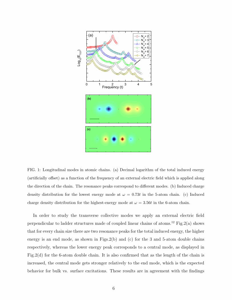
Let us first focus on the dielectric response function in linear chains of atoms, with the
intent to identify the basic features of their collective excitations. The frequency dependence
of the induced energy in such systems, exposed to a driving electric field along the chain
direction, is shown in Fig.1(a). It exhibits a series of resonances, which increase in number
for chains with increasing length. As observed in the spatial charge density distribution, e.g.
shown for the 5-atom chain in Fig.1(b), the lowest peak corresponds to a dipole resonance.
When increasing the system size, the dipole peak moves to lower frequencies, which is
the expected finite-size scaling behavior. The resonances at higher frequency correspond
to higher harmonic charge density distributions. For example, in Fig.1(c), we show the
charge density distribution corresponding to the highest frequency resonance of the 6-atom
chain. In contrast to the dipole resonance, these modes show a rapidly oscillating charge
density distribution, and thus have the potential to provide spatial localization of collective
excitations in more sophisticated structures. While an extension to much larger chains
is numerically prohibitive within the current method, the finite-size scaling of the observed
dielectric response of these clusters is consistent with the 1D bulk expectation of a dominant
low-energy plasmon mode, coexisting with a particle-hole continuum of much weaker spectral
intensity.
5
0 1 2 3 4 5
(c)
(b)
(a)
Log 10
(ETO
T)
Frequency (t)
Nat= 2 Nat= 3 Nat= 4 Nat= 5 Nat= 6 Nat= 7
FIG. 1: Longitudinal modes in atomic chains. (a) Decimal logarithm of the total induced energy
(artificially offset) as a function of the frequency of an external electric field which is applied along
the direction of the chain. The resonance peaks correspond to different modes. (b) Induced charge
density distribution for the lowest energy mode at ω = 0.73t in the 5-atom chain. (c) Induced
charge density distribution for the highest-energy mode at ω = 3.56t in the 6-atom chain.
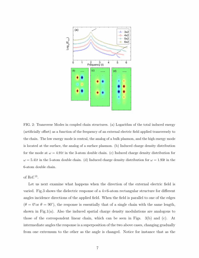
In order to study the transverse collective modes we apply an external electric field
perpendicular to ladder structures made of coupled linear chains of atoms.12 Fig.2(a) shows
that for every chain size there are two resonance peaks for the total induced energy, the higher
energy is an end mode, as shown in Figs.2(b) and (c) for the 3 and 5-atom double chains
respectively, whereas the lower energy peak corresponds to a central mode, as displayed in
Fig.2(d) for the 6-atom double chain. It is also confirmed that as the length of the chain is
increased, the central mode gets stronger relatively to the end mode, which is the expected
behavior for bulk vs. surface excitations. These results are in agreement with the findings
6
0 1 2 3 4 5 6
(d)
(c)(b)
(a)
Log 10
(ETO
T)Frequency (t)
3x2 4x2 5x2 6x2
FIG. 2: Transverse Modes in coupled chain structures. (a) Logarithm of the total induced energy
(artificially offset) as a function of the frequency of an external electric field applied transversely to
the chain. The low energy mode is central, the analog of a bulk plasmon, and the high energy mode
is located at the surface, the analog of a surface plasmon. (b) Induced charge density distribution
for the mode at ω = 4.91t in the 3-atom double chain. (c) Induced charge density distribution for
ω = 5.41t in the 5-atom double chain. (d) Induced charge density distribution for ω = 1.93t in the
6-atom double chain.
of Ref.13.
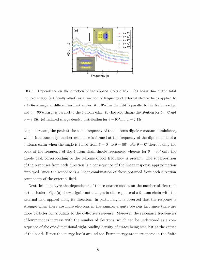
Let us next examine what happens when the direction of the external electric field is
varied. Fig.3 shows the dielectric response of a 4×6-atom rectangular structure for different
angles incidence directions of the applied field. When the field is parallel to one of the edges
(θ = 0°or θ = 90°), the response is essentially that of a single chain with the same length,
shown in Fig.1(a). Also the induced spatial charge density modulations are analogous to
those of the correspondent linear chain, which can be seen in Figs. 3(b) and (c). At
intermediate angles the response is a superposition of the two above cases, changing gradually
from one extremum to the other as the angle is changed. Notice for instance that as the
7
0 2 4 6 8
(b)
(c)
(a)
Log 10
(ETO
T)
Frequency (t)
= 00
= 200
= 450
= 700
= 900
FIG. 3: Dependence on the direction of the applied electric field. (a) Logarithm of the total
induced energy (artificially offset) as a function of frequency of external electric fields applied to
a 4×6-rectangle at different incident angles. θ = 0°when the field is parallel to the 4-atoms edge,
and θ = 90°when it is parallel to the 6-atoms edge. (b) Induced charge distribution for θ = 0°and
ω = 3.15t. (c) Induced charge density distribution for θ = 90°and ω = 2.15t.
angle increases, the peak at the same frequency of the 4-atoms dipole resonance diminishes,
while simultaneously another resonance is formed at the frequency of the dipole mode of a
6-atoms chain when the angle is tuned from θ = 0° to θ = 90°. For θ = 0° there is only the
peak at the frequency of the 4-atom chain dipole resonance, whereas for θ = 90° only the
dipole peak corresponding to the 6-atoms dipole frequency is present. The superposition
of the responses from each direction is a consequence of the linear response approximation
employed, since the response is a linear combination of those obtained from each direction
component of the external field.
Next, let us analyze the dependence of the resonance modes on the number of electrons
in the cluster. Fig.4(a) shows significant changes in the response of a 9-atom chain with the
external field applied along its direction. In particular, it is observed that the response is
stronger when there are more electrons in the sample, a quite obvious fact since there are
more particles contributing to the collective response. Moreover the resonance frequencies
of lower modes increase with the number of electrons, which can be understood as a con-
sequence of the one-dimensional tight-binding density of states being smallest at the center
of the band. Hence the energy levels around the Fermi energy are more sparse in the finite
8

0 1 2 3 4-6
-5
-4
-3
-2
-1
0
1
2
3 (c)
(b)
(a)
Log 10
(ETO
T)
Frequency (t)
Nel=1
Nel=3
Nel=5
Nel=7
Nel=9
FIG. 4: Variation of the number of electrons. (a) Logarithm of the total induced energy as a
function of the external electric field frequency. The number of electrons Nel in a 9-atom chain
is varied. (b) Induced charge density distribution for Nel = 1 at ω = 0.36t. (c) Induced charge
density distribution for Nel = 9 at ω = 0.53t.
system, and therefore the excitations require larger frequencies at half-filling. The same
does not hold for higher frequency modes since these correspond to transitions between the
lowest and highest levels for any number of electrons in the sample. Therefore these modes
have the same frequency, independent of the electronic filling. Higher filling also allows
the induced charge density to concentrate closer to the boundaries of the structure, as a
comparison between Figs.4(b) and (c) demonstrates. Fig.4(b) shows that a 9-atoms chain
with Nel = 1 electron has its induced charge density localized around the center of the
chain. In contrast, Fig.4(c) displays the induced charge density localized at the boundaries
of the same structure with Nel = 9. This concentration closer to the surface happens be-
cause higher energy states have a stronger charge density modulation than the lower energy
ones. Therefore the induced charge density is more localized for higher fillings, because at
low fillings the excitations responsible for the induced charge density are between the more
homogeneous lower energy levels. This can be interpreted as a finite-size rendition of the
fact that by increasing the electronic filling one obtains the classical response with all the
induced charge density on the surface of the object.
Access to high energy states is very important for achieving spatial localization of the
induced charge density, as the next example shows. In order to find a structure with spatially
9
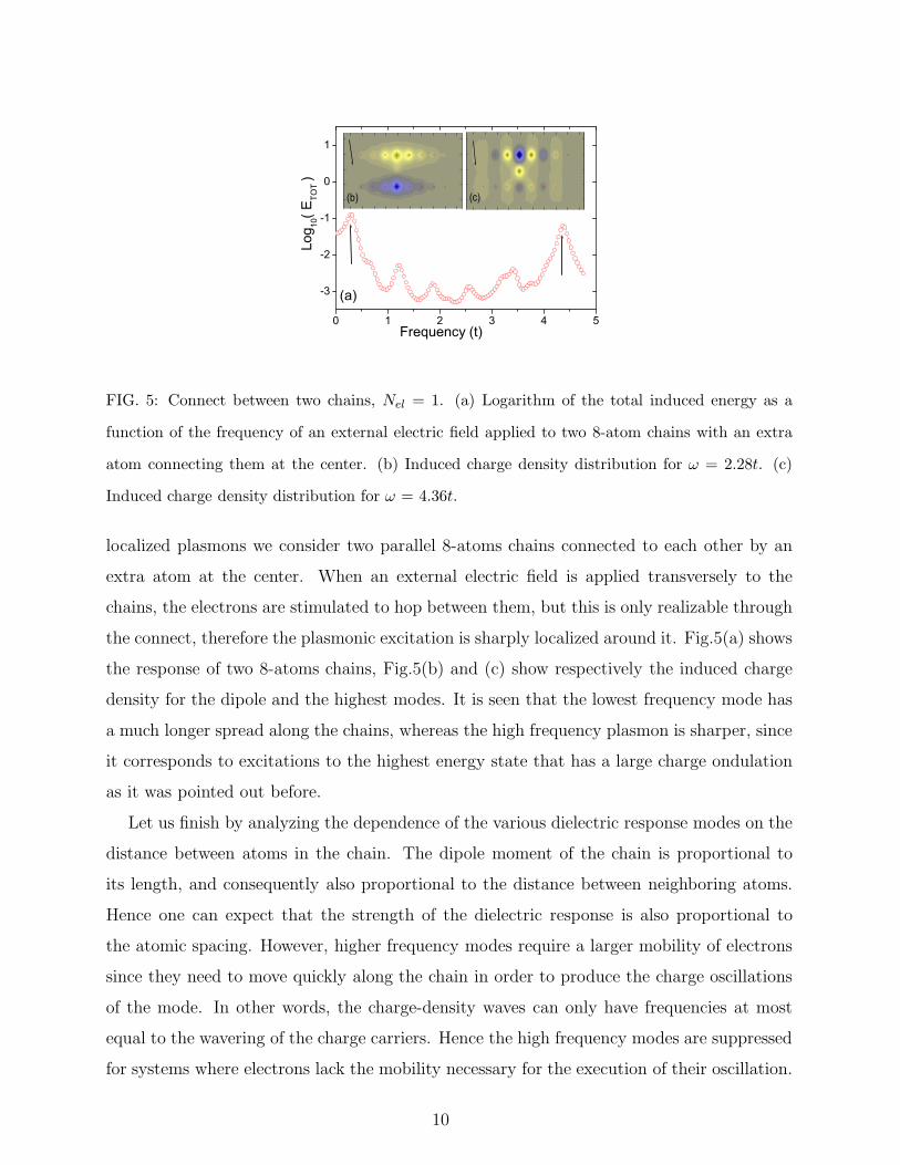
0 1 2 3 4 5
-3
-2
-1
0
1
(b)
(c)
(a)
Log 10
( ETO
T )
Frequency (t)
FIG. 5: Connect between two chains, Nel = 1. (a) Logarithm of the total induced energy as a
function of the frequency of an external electric field applied to two 8-atom chains with an extra
atom connecting them at the center. (b) Induced charge density distribution for ω = 2.28t. (c)
Induced charge density distribution for ω = 4.36t.
localized plasmons we consider two parallel 8-atoms chains connected to each other by an
extra atom at the center. When an external electric field is applied transversely to the
chains, the electrons are stimulated to hop between them, but this is only realizable through
the connect, therefore the plasmonic excitation is sharply localized around it. Fig.5(a) shows
the response of two 8-atoms chains, Fig.5(b) and (c) show respectively the induced charge
density for the dipole and the highest modes. It is seen that the lowest frequency mode has
a much longer spread along the chains, whereas the high frequency plasmon is sharper, since
it corresponds to excitations to the highest energy state that has a large charge ondulation
as it was pointed out before.
Let us finish by analyzing the dependence of the various dielectric response modes on the
distance between atoms in the chain. The dipole moment of the chain is proportional to
its length, and consequently also proportional to the distance between neighboring atoms.
Hence one can expect that the strength of the dielectric response is also proportional to
the atomic spacing. However, higher frequency modes require a larger mobility of electrons
since they need to move quickly along the chain in order to produce the charge oscillations
of the mode. In other words, the charge-density waves can only have frequencies at most
equal to the wavering of the charge carriers. Hence the high frequency modes are suppressed
for systems where electrons lack the mobility necessary for the execution of their oscillation.
10
0 2 4 6-4
-3
-2
-1
0
1
2
3
Log 10
(ETO
T)
Frequency (t3)
a = 2.5rB
a = 3.0rB
a = 3.5rB
a = 4.0rB
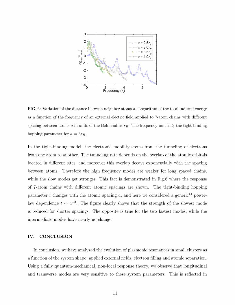
FIG. 6: Variation of the distance between neighbor atoms a. Logarithm of the total induced energy
as a function of the frequency of an external electric field applied to 7-atom chains with different
spacing between atoms a in units of the Bohr radius rB . The frequency unit is t3 the tight-binding
hopping parameter for a = 3rB .
In the tight-binding model, the electronic mobility stems from the tunneling of electrons
from one atom to another. The tunneling rate depends on the overlap of the atomic orbitals
located in different sites, and moreover this overlap decays exponentially with the spacing
between atoms. Therefore the high frequency modes are weaker for long spaced chains,
while the slow modes get stronger. This fact is demonstrated in Fig.6 where the response
of 7-atom chains with different atomic spacings are shown. The tight-binding hopping
parameter t changes with the atomic spacing a, and here we considered a generic14 power-
law dependence t ∼ a−3. The figure clearly shows that the strength of the slowest mode
is reduced for shorter spacings. The opposite is true for the two fastest modes, while the
intermediate modes have nearly no change.
IV. CONCLUSION
In conclusion, we have analyzed the evolution of plasmonic resonances in small clusters as
a function of the system shape, applied external fields, electron filling and atomic separation.
Using a fully quantum-mechanical, non-local response theory, we observe that longitudinal
and transverse modes are very sensitive to these system parameters. This is reflected in
11
their frequency, oscillator strength and the spatial modulation of the induced charge density.
Specifically, we identify bulk and surface plasmonic excitations which can be controlled in
amplitude and frequency by the cluster size. Furthermore, we observe a non-trivial filling
dependence, which critically depends on the electronic level spacing in a given structure.
We also find that changes in atomic spacings strongly affect the electron mobility in these
structures, with a very different impact on low-energy vs. high-energy modes. And we
see that changing the position of a single atom in a nanostructure can completely alter its
collective dielectric response. This strong sensitivity to small changes is the key to controlling
the modes of ultra-small structures, and it can thus become the gateway to a new generation
of quantum devices which effectively utilize quantum physics for new functionalities.
Acknowledgments
We would like to thank Gene Bickers, Richard Thompson, Vitaly Kresin, Aiichiro Nakano
amd Yung-Ching Liang for useful conversations, and we acknowledge financial support by the
Department of Energy, grant number DE-FG02-06ER46319. The numerical computations
were carried out on the University of Southern California high-performance computer cluster.
∗ Electronic address: [email protected]
1 V.V. Kresin, Phys. Rep. 220, 1 (1992); K.D. Bonin and V.V. Kresin, “Electric-Dipole Polariz-
abilities of Atoms, Molecules and Clusters” (World Scientific, Singapore, 1997).
2 G.V. Nazin, X.H. Oiu, and W. Ho, Science 302, 77 (2003); G.V. Nazin, X.H. Oiu, and W. Ho,
Phys. Rev. Lett. 90, 216110 (2003); N. Nilius, T.M. Wallis, M. Persson, and W. Ho, Phys. Rev.
Lett. 90, 196103 (2003); N. Nilius, T.M. Wallis, and W. Ho, Science 297, 1853 (2002).
3 J. Homola, S.S. Yee, and G. Gauglitz, Sensors & Actuators: B 54, 3 (1999).
4 C.R. Moon, L.S, Mattos, B.K. Foster, G. Zeltzer, W. Ko, and H.C. Monoharan, Science 319,
782 (2008).
5 A. K. Sarychev and V. M. Shalaev, “Electrodynamics of Metamaterials” (World Scientific,
Singapore, 2007).
6 I. Grigorenko, S. Haas and A.F.J. Levi, Phys. Rev. Lett. 97, 036806 (2006); A. Cassidy, I.
12
Grigorenko, and S. Haas, Phys. Rev. B 77, 245404 (2008); I. Grigorenko, S. Haas, A.V. Balatsky,
and A.F.J. Levi, New J. Phys. 10, 043017 (2008).
7 J.C. Slater and G.F. Koster, Phys. Rev. 94, 1498 (1954); C.M. Goringe, D.R. Bowler and E.
Hernndez, Rep. Prog. Phys. 60, 1447 (1997); N. W. Ashcroft and N. D. Mermin, “Solid State
Physics” (Thomson Learning, 1976).
8 G. Mie, Annalen der Physik, 25, 377 (1908).
9 D. M. Wood and W. R. Ashcroft, Phys. Rev. B 25, 6255 (1982); M. J. Rice, W. R. Schneider,
and S. Strassler, Phys. Rev. B 8, 474 (1973); S. Das Sarma, Phys. Rev. B 43, 11768 (1991); D.
R. Fredkin and L. D. Mayergoyz, Phys. Rev. Lett. 91, 253902 (2003).
10 S. Nie and S. R. Emory, Science 275, 1102 (1997).
11 W. H. Press, B. P. Flanney, S. A. Teukolsky, W. T. Vetterling, “Numerical Recipes” (Cambridge
University Press, 1988).
12 Within the current approach, at least two coupled chains are necessary to visualize charge
redistributions along the transverse direction, since charge fluctuations within the orbitals are
not accounted for.
13 J. Yan, Z. Yuan and S. Gao, Phys. Rev. Lett. 98, 216602 (2007).
14 W.A. Harrison, “Electronic Structure and the Properties of Solids” (W. H. Freeman, San Fran-
cisco, 1980).
13