physics and application of plasmas based on pulsed power
TRANSCRIPT
Physics and Application of Plasmas
Based on Pulsed Power Technology
Edited by Eiki Hotta and Tetsuo Ozaki
December 21-22, 2010
National Institute for Fusion Science
Toki, Gifu, Japan
Abstract
The papers presented at the symposium on “Physics and Application of Plasmas Based
on Pulsed Power Technology” held on December 21-22, 2010 at National Institute of
Fusion Science are collected. The papers in this proceeding reflect the current status and
progress in the experimental and theoretical researches on high power particle beams
and high energy density plasmas produced by pulsed power technology.
Keyword: high power particle beams, high energy density plasma, pulsed power
technology, z-pinch, soft x-ray, EUV, x-ray laser, pulsed discharge, high power micro
wave, material processing, medical application
Preface
The symposium entitled “Physics and Application of Plasmas Based on Pulsed Power
Technology” was organized as a part of the General Collaborative Research of National
Institute for Fusion Science (NIFS) and held on December 21-22, 2010 at NIFS, Toki.
In the symposium, 23 papers were presented in two days, of which 22 papers are
reported in this proceeding. The total number of participants was 47 including students
and researchers from universities and companies.
The main objective of the symposium is to provide a place of discussion about the
pulsed power technology, generation of plasmas by using pulsed power technology and
its application. Therefore, the papers in this proceeding reflect the current status and
progress in the experimental and theoretical researches on high power particle beams
and high energy density plasmas produced by pulsed power technology in Japan. It is
our great pleasure with the unexpectedness if the symposium was beneficial to the
development of pulsed power technology.
We would like to express our sincere thanks to all of the participants, the authors and
the staff of NIFS.
Thank you very much.
Eiki Hotta
Department of Energy Sciences
Tokyo Institute of Technology
Tetsuo Ozaki
National Institute for Fusion Science

List of Participants
K. Takaki Iwate University
I. Yagi Iwate University
H. Aoki Iwate University
S. Ihara Saga University
W. Jiang Nagaoka University of Technology
G. Imada Niigata Institute of Technology
K. Satoh Niigata Institute of Technology
M. Onda Niigata Institute of Technology
T. Kikuchi Nagaoka University of Technology
S. Furuya Gunma University (Present: Saitama Institute of Technology)
N. Tashiro Gunma University
K. Masugata University of Toyama
H. Ito University of Toyama
H. Yamamoto University of Toyama
Y. Ochiai University of Toyama
H.M. Liu Toyama University
T. Kawamura Tokyo Institute of Technology
T. Ozawa Tokyo Institute of Technology
K. Kamada Kanazawa University
R. Ando Kanazawa University
Y. Soga Kanazawa University
K. Nose Kanazawa University
K. Misawa Kanazawa University
S. Yanagi Kanazawa University
K. Kato Kanazawa University
T. Kitamura Kanazawa University
N. Yamada Kanazawa University
M. Kato Kanazawa University
T. Mimura Kanazawa University
K. Horioka Tokyo Institute of Technology
H. Sakai Tokyo Institute of Technology
Y. Ogata Tokyo Institute of Technology
A. Nakayama Tokyo Institute of Technology

Y. Kuroda Tokyo Institute of Technology
K. Takasugi Nihon University
M. Nishio Nihon University
H. Sakuma Nihon University
M. Iwata Nihon University
E. Hotta Tokyo Institute of Technology
H. Kumai Tokyo Institute of Technology
J. Li Tokyo Institute of Technology
A. Tokuchi Pulse Power Technology Lab.
T. Tazima National Institute for Fusion Science
T. Ozaki National Institute for Fusion Science
H. Akiyama Kumamoto University
M. Akiyama Kumamoto University
T. Ihara Kumamoto University
Contents
Mechanism of Destruction on Ice Breaking Using Pulsed Power 1
S. Ihara, Y. Kominato, K. Fukuda (Saga University), and S. Ushio (National
Institute of Polar Research)
Experimental Study on Underwater Shock Wave Generated by Using
Pulse Power Technology
5
H. Yamamoto, Y. Nakaya, H. Ito, and K. Masugata (University of Toyama)
Discharge Phenomena in Supercritical Carbon Dioxide 9
T. Ihara, T. Kiyan, S. Katsuki, M. Hara, and H. Akiyama (Kumamoto University)
Production of Metal Contained Carbon Plasma Using Shunting Arc
Discharge for Composite Film Preparation
13
H. Aoki, K. Takahashi, and K. Takaki (Iwate University)
Application of Triboluminescence to Roentgen Diagnosis 18
N. Tashiro and S. Furuya (Saitama Institute of Technology)
Laser Target using Continuous Supersonic Jet 22
Y. Ogata, K. Takahashi (Tokyo Institute of Technology), H. Kuwabara (IHI
Corporation), M. Nakajima, and K. Horioka (Tokyo Institute of Technology)
Ion Acceleration Independent of the Direction of Electric Currents in
Gas-puff Z-pinch
26
M. Nishio, K. Takasugi, and H. Sakuma (Nihon University)
Characteristics of Nano-second Pulsed Discharge Using All Solid State
Pulsed Power Generator
30
I. Yagi, K. Takaki (Iwate University), T. Namihara (Kumamoto University), and R.
Ono (The University of Tokyo)
Electrical Conductivity Measurements of Warm Dense Matter with
Semi-rigid Vessel
36
H. Sakai, K. Iwasaki, M. Nakajima, T. Kawamura, and K. Horioka (Tokyo Institute
of Technology)
Pulsed Power Generator Using Solid-State LTD Modules 40
W. Jiang and A. Tokuchi (Nagaoka University of Technology)
Development of MOS-FET Based Marx Generator with Self-Proved
Gate Power
43
A. Tokuchi (Pulsed Power Japan Laboratory Ltd.), W. Jiang (Nagaoka University
of Thechnology), K. Takayama, T. Arai, T. Kawakubo, and T. Adachi (High Energy
Accelerator Research Organization (KEK))
Design of Bragg Resonator for Free Electron Maser 48
K. Nose, K. Misawa, S. Yanagi, K. Kato, T. Kitamura, N. Yamada, Y. Soga, K.
Kamada (Kanazawa University), M. Yoshida (High Energy Accelerator Research
Organization), and N.S. Ginzburg (Institute of Applied Physics, Russian Academy
of Science)
Development of 100 GHz Interdigital Backward-Wave Oscillator 54
M. Kato, Y. Soga, T. Mimura, Y. Kato, K. Kamada (Kanazawa University), and M.
Yoshida (High Energy Accelerator Research Organization)
Longitudinal Bunch Compression Study with Induction Voltage
Modulator
59
A. Nakayama, Y. Miyazaki (Tokyo Institute of Technology), T. Kikuchi (Nagaoka
University of Technology), M. Nakajima, and K. Horioka (Tokyo Institute of
Technology)
Theoretical Study on Population Inversion of Hydrogen-like Nitrogen
in Recombination Plasma
63
T. Ozawa, Y. Ishizuka, H. Kumai, E. Hotta, K. Horioka, and T. Kawamura (Tokyo
Institute of Technology)
Analysis of Highly Ionized N Plasma Spectra under the Effect of an
External Magnetic Field in Fast Capillary Discharge
67
H. Kumai, Y. Ishizuka, M. Watanabe and E. Hotta (Tokyo Institute of Technology)
Counter-facing Plasma Guns for Efficient Extreme Ultra-Violet Plasma
Light Source
73
Y. Kuroda, K. Hayashi (Tokyo Institute of Technology), H. Kuwabara (IHI
Corporation), M. Nakajima, T. Kawamura, and K. Horioka (Tokyo Institute of
Technology)
Characterization of the Pulsed Ion Beam in a Plasma Focus Device for
Al Surface Modification
77
H.M. Liu, D.X. Cheng, H. Ito, and K. Masugata (Toyama University)
Characteristics of an Atmospheric Pulsed DBD Plasma Jet and Its
Preliminary Application for Sterilization
82
J. Li, N. Sakai, M. Watanabe, E. Hotta, and M. Wachi (Tokyo Institute of
Technology)
Treatment of Zooplankton in Water by Pulsed Power -An Effect of
NaHCO3 Additive for Micro Bubble Production-
88
K. Satoh, M. Onda, S. Sakai, and G. Imada (Niigata Institute of Technology)
Applications of Pulsed Intense Relativistic Electron Beam to Aquatic
Conservation
93
T. Kikuchi, H. Kondo, T. Sasaki (Nagaoka University of Technology), H. Moriwaki
(Shinshu University), G. Imada (Niigata Institute of Technology), and N. Harada
(Nagaoka University of Technology)
Development of Exploding Wire Ion Source for Intense Pulsed Heavy
Ion Beam Accelerator
99
Y. Ochiai, T. Murata, H. Ito, and K. Masugata (University of Toyama)
Mechanisms of Destruction on Ice breaking using Pulsed Power
Satoshi Ihara, Yuichi Kominato, Kazuyuki Fukuda, Shuki Ushio*
Saga University
*National Institute of Polar Research
ABSTRACTIn this research, investigation on breaking of ice using a pulsed power generator as a navigation of
ice-breaker at ice-covered ocean, was described. In these experiments, pulsed arc discharge was formed by Marx generator. In order to investigate the dependence of input energy required for ice breaking on circuit parameters of generator, the capacitance of generator was changed. The input energy for ice-breaking was calculated from waveforms of electric power. It was found that the input energy for ice-breaking decreased as the peak power increased with decrease of the capacitance of generator.
Keywordspulsed power, ice, shock wave
1. Introduction The development of navigation systems for icebreakers on icebound sea has been important for the advancement of natural resources production, economic activities and so on. To make possible the navigation in ice-covered ocean, an icebreaker crushes the sea ice using the force generated by the ship’s mass [1-3].
In this research, investigation on ice breaking using a pulsed power as a navigation of icebreaker at ice-covered ocean was curried out. In the previous researches, the ice breaking using Marx generator has been demonstrated experimentally [4-5]. In order to reduce the energy of ice breaking, understanding mechanisms of ice breaking is required.
Generally air bubbles is one of the very important parameters for strength of ice. In this paper, experimental result on influences of air bubbles in ice were described. The energy required to break specimen of ice was obtained on ice with and without air bubbles. Furthermore crack formation inside ice was observed by high speed camera.
2. Experimental Setup Figure 1 shows a configuration of the
experimental apparatus which consists of pulsed power generator, plastic water vessel, electrodes and measuring devices. A Marx generator, with six capacitors with a capacitance of 0.22 �F, was used as a pulsed power generator. The ice sample was placed in a plastic water vessel, which was filled with tap water. Electrodes were placed at 20 mm from surface of ice specimen as shown in Fig. 2. The electrodes were made of a dielectric material (polyethylene) and metal (copper). The distance between electrodes was 45 mm.
Figure 3 shows typical specimens of ice with size of 7x7x13cm, used in the experiments. Two kinds of ice with and without bubbles as shown in Fig. 3 were tested. At thin ice specimen, specimen is destructed in only one shot of generator. The number of shot for breaking increase with thickness of specimen. Fig. 4 shows the typical broken specimen after several shots.
11
Fig. 1. Configuration of the experimental apparatus.
Water(3 to 4�)
Ice sample
45mm
electrode
20mm
Fig. 2. Setting of ice specimen and electrodes.
(a) Clear ice
(b) Ice with bubbles
Fig. 3. Typical specimens of ice.
Fig. 4. Typical specimen broken in testing.
3. Results and Discussion 3.1 Characteristics of energy for ice breaking
Figure 5 shows characteristics of energy for ice breaking on pressure of shock wave on clear ice and ice with bubbles when the charging energy was constant. The pressure of shock wave indicated at horizontal axis was estimated from Hugoniot’s equation using velocity of shock wave. It is found that the Eib decreases with increase of pressure of shock wave at the both types of ice, and Eib was about 0.5 times lower when the ice with bubbles was used than when the clear ice was used. The decrease of Eib suggests that efficient ice breaking was realized.
500 600 700 800 900 1000 11000
5
10
15
�
�
Ene
rgy
for i
ce b
reak
ing E
ib [k
J]
Pressure of shock wave Psw [MPa]
Clear ice
Ice with bubbles
Fig. 5. Characteristics of energy for ice breaking on pressure of shock wave.
3.2 Observation of crack formation
Figure 6 shows the configuration of apparatus for taking photograph of crack formation at inside ice. High speed camera (SIMD16, Specialised lmaging Limited) was used for observation of crack.
Figure 7 show photographs and waveforms when the clear ice are used. First photograph of Fig. 7(a) shows the ice at no discharge, and photo 1, 2, 3 show the images at after 17.5, 24.0 and 30.5��s from onset
22
of discharge current, respectively. Gate pulses, which correspond to shutter timing, are shown in Fig. 7 (b) with voltage and current waveforms. In photo 1 cracks can be observed at upper side of ice, and the cracks propagated in ice.
Clear Ice
Current probe
Gate signal To oscilloscope
Back light source
Fig. 6. Schematic diagram of apparatus for taking photograph of crack formation at inside ice.
Reference 1
2 3
Ice20mm
20mm
20mm 20mm
Crack
electrodes
Crack Crack
(a) Photographs of crack formation in clear ice. (b)
-10 0 10 20 30 40-100
-50
0
50
100
150
200
Time t [�s]
App
lied
Vol
tage
V [k
V]G
ate
sign
al V
gs [a
.u.]
-2
0
2
4
Cur
rent
I [k
A]
1 2 3Gate Signal
(b) Waveforms of voltage, current and gate signal of camera.
Fig. 7. Photographs and waveforms when the clear ice are used.
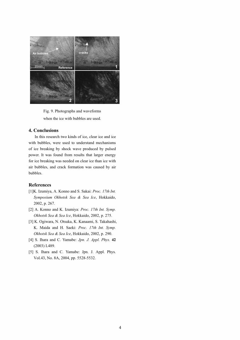
Figure 8 (a) and (b) show photographs of crack formation in ice with bubbles, and voltage, current and gate pulse waveforms. In photo 1 no cracks were found in ice. In photo 2 cracks can be observed, and propagated in ice. Fig. 9 shows detail of crack formation in ice. In these photos, it was found that cracks were formed along air bubbles. We can explain these phenomena as follows. When the shock wave propagates in ice, the wave refracts at air bubble. At that time the stress is applied to ice, and then the structure of ice is destructed locally, that lead to formation of cracks. It was found that crack formation is caused by air bubbles inside ice cause.
1
2 3
Reference
Ice
20mm
Crack
Air bubble
electrodes
Crack
(a) Photographs of crack formation in ice with bubbles.
-10 0 10 20 30 40-100
-50
0
50
100
150
200
Time t [�s]
Appl
ied
Volta
ge V
[kV]
Gat
e si
gnal
Vgs
[a.u
.]
-2
0
2
4C
urre
nt I
[kA]
1 2 3Gate Signal
(b) Waveforms of voltage, current and gate signal of camera.
Fig. 8. Photographs and waveforms when the ice with bubbles are used.
33
1
2 3
Air bubbles
20mm
cracks
Reference
Fig. 9. Photographs and waveforms
when the ice with bubbles are used.
4. Conclusions In this research two kinds of ice, clear ice and ice with bubbles, were used to understand mechanisms of ice breaking by shock wave produced by pulsed power. It was found from results that larger energy for ice breaking was needed on clear ice than ice with air bubbles, and crack formation was caused by air bubbles.
References[1]K. Izumiya, A. Konno and S. Sakai: Proc. 17th Int.
Symposium Okhotsk Sea & Sea Ice, Hokkaido, 2002, p. 267.
[2] A. Konno and K. Izumiya: Proc. 17th Int. Symp. Okhotsk Sea & Sea Ice, Hokkaido, 2002, p. 275.
[3] K. Ogiwara, N. Otsuka, K. Kanaami, S. Takahashi, K. Maida and H. Saeki: Proc. 17th Int. Symp. Okhotsk Sea & Sea Ice, Hokkaido, 2002, p. 290.
[4] S. Ihara and C. Yamabe: Jpn. J. Appl. Phys. 42(2003) L489.
[5] S. Ihara and C. Yamabe: Jpn. J. Appl. Phys. Vol.43, No. 8A, 2004, pp. 5528-5532.
44
Experimental Study on Underwater Shock Wave Generated by Using Pulse Power Technology
H. Yamamoto, Y. Nakaya, H. Ito and K. Masugata
Dep. of Electrical and Electronic Engineering, University of Toyama, 3190 Gofuku, Toyama 930-8555, Japan
ABSTRACT Applications of underwater shock waves have been extended to various industrial, medical and environmental fields. The underwater shock wave is easily generated by means of explosion of explosives or high voltage electric discharge in water. In order to generate the underwater shock wave with high pressure and good controllability, we have developed the underwater shock wave system utilizing the pulse power machine which consists of a Marx generator and a pulse forming line. Characteristics of the underwater shock wave generated by the pulsed electric discharge in water are studied by a polyvinyliden-difluoride pressure transducer. When the Marx generator was operated at 120 kV and the discharge gap distance was d=7 mm, the underwater shock with peak pressure of 122 MPa and average velocity of 2100 m/s and a half-width of 2.5 �swas obtained at 30 mm downstream from the axis.
KeywordsUnderwater shock wave, ultrasound wave, pulse power technology
1. Introduction The subject of the generation of strong shock waves has already been of continuous interest for more than 100 years due to its important potential applications in basic and applied research related to equations of state, plasma and space physics. In a laboratory environment, there are several methods of shock wave generation, for instance, chemical explosions [1,2], laser irradiation of a target [3], the Z-pinch approach [4], and underwater electrical explosions of wires [5]. In the latter case, underwater shock waves with several tens of megapascals were generated using moderate pulsed power generators with stored energy of only several kilojoules. A high shock wave pressure in water is realized due to underwater explosion of explosives (wire) and/or quick release of high current at the high voltage electric power in water. The small compressibility of water and the relatively slight decay of a shock wave during its propagation make the shock wave attractive for various practical applications.
The pulsed power technology has been developed over the last two decades primarily for nuclear fusion and high energy density physics research. Advances in pulsed power technology have led us to a number of potential applications such as intense pulsed charged particle beam, discharge light source (EUV source), gas laser, pulsed ozonizer and exhaust gases cleaning. The developed high-voltage pulsed power generators can cause the electrical discharge breakdown in liquid medium, such as water and dielectric oil. The discharge in liquid follows some physical phenomena, such as an intense electric field at a tip of discharge column, a radical formation in discharge channel, an ultra violet radiation from discharge and a shockwave generation on boundary between plasma and liquid medium. These phenomena are very attractive for variety of industry, medical and environmental applications. In using underwater shock wave for various applications, the control of strength and the pulse duration of the underwater shock wave are the most
55
important parameter. In order to generate the underwater shock wave with high pressure and good controllability, we have developed the underwater shock wave system utilizing the pulse power machine which consists of a Marx generator and a pulse forming line. In this paper, we report characteristics of the underwater shock wave measured by a polyvinyliden-difluoride pressure transducer.
2. Experimental Setup Figure 1 shows a schematic configuration of
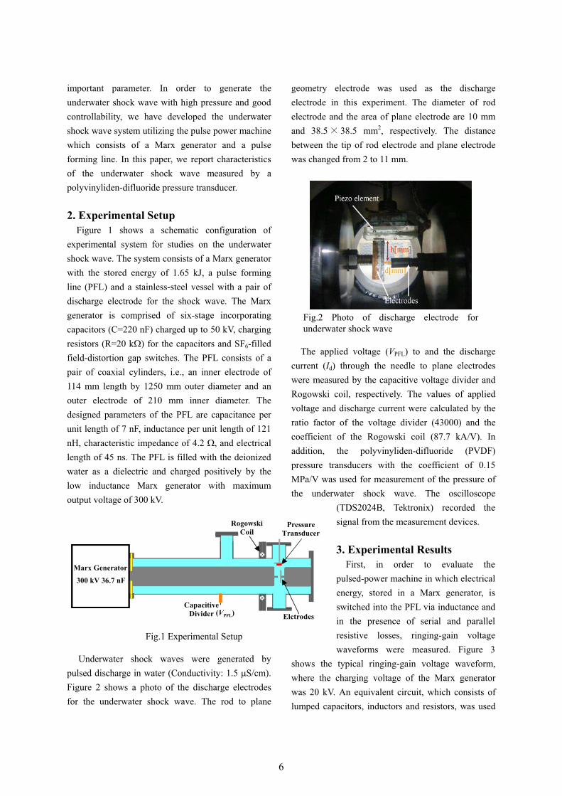
experimental system for studies on the underwater shock wave. The system consists of a Marx generator with the stored energy of 1.65 kJ, a pulse forming line (PFL) and a stainless-steel vessel with a pair of discharge electrode for the shock wave. The Marx generator is comprised of six-stage incorporating capacitors (C=220 nF) charged up to 50 kV, charging resistors (R=20 k�) for the capacitors and SF6-filled field-distortion gap switches. The PFL consists of a pair of coaxial cylinders, i.e., an inner electrode of 114 mm length by 1250 mm outer diameter and an outer electrode of 210 mm inner diameter. The designed parameters of the PFL are capacitance per unit length of 7 nF, inductance per unit length of 121 nH, characteristic impedance of 4.2 �, and electrical length of 45 ns. The PFL is filled with the deionized water as a dielectric and charged positively by the low inductance Marx generator with maximum output voltage of 300 kV.
Underwater shock waves were generated by pulsed discharge in water (Conductivity: 1.5 �S/cm). Figure 2 shows a photo of the discharge electrodes for the underwater shock wave. The rod to plane
geometry electrode was used as the discharge electrode in this experiment. The diameter of rod electrode and the area of plane electrode are 10 mm and 38.5 38.5 mm2, respectively. The distance between the tip of rod electrode and plane electrode was changed from 2 to 11 mm.
The applied voltage (VPFL) to and the discharge current (Id) through the needle to plane electrodes were measured by the capacitive voltage divider and Rogowski coil, respectively. The values of applied voltage and discharge current were calculated by the ratio factor of the voltage divider (43000) and the coefficient of the Rogowski coil (87.7 kA/V). In addition, the polyvinyliden-difluoride (PVDF) pressure transducers with the coefficient of 0.15 MPa/V was used for measurement of the pressure of the underwater shock wave. The oscilloscope
(TDS2024B, Tektronix) recorded the signal from the measurement devices.
3. Experimental Results First, in order to evaluate the
pulsed-power machine in which electrical energy, stored in a Marx generator, is switched into the PFL via inductance and in the presence of serial and parallel resistive losses, ringing-gain voltage waveforms were measured. Figure 3
shows the typical ringing-gain voltage waveform, where the charging voltage of the Marx generator was 20 kV. An equivalent circuit, which consists of lumped capacitors, inductors and resistors, was used
Marx Generator
300 kV 36.7 nF
CapacitiveDivider (VPFL)
RogowskiCoil
Elctrodes
PressureTransducer
Fig.1 Experimental Setup
Fig.2 Photo of discharge electrode for underwater shock wave
66
which allows the determination of three unknown electrical parameters from two decay constants and the frequency of an oscillatory component calculated from the ringing-gain waveform. As seen in Fig. 3, the ringing period is about 500 ns, which gives the lumped inductance of 892 nH. Taking the PFL’s inductance of 152 nH into account, the Marx generator is estimated to be 740 nH. From two decay constants of ringing voltage waveform, serial and parallel resistances of the equivalent circuit are estimated to be 0.82 � and 130 �, respectively.
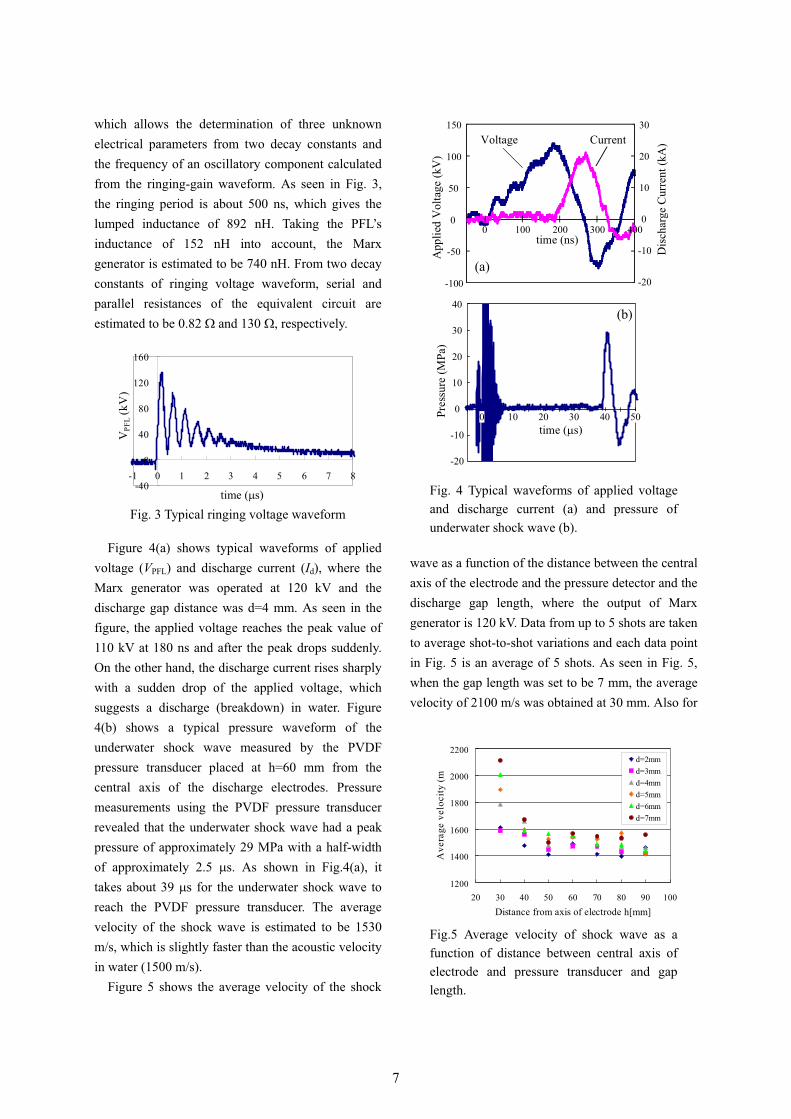
Figure 4(a) shows typical waveforms of applied voltage (VPFL) and discharge current (Id), where the Marx generator was operated at 120 kV and the discharge gap distance was d=4 mm. As seen in the figure, the applied voltage reaches the peak value of 110 kV at 180 ns and after the peak drops suddenly. On the other hand, the discharge current rises sharply with a sudden drop of the applied voltage, which suggests a discharge (breakdown) in water. Figure 4(b) shows a typical pressure waveform of the underwater shock wave measured by the PVDF pressure transducer placed at h=60 mm from the central axis of the discharge electrodes. Pressure measurements using the PVDF pressure transducer revealed that the underwater shock wave had a peak pressure of approximately 29 MPa with a half-width of approximately 2.5 �s. As shown in Fig.4(a), it takes about 39 �s for the underwater shock wave to reach the PVDF pressure transducer. The average velocity of the shock wave is estimated to be 1530 m/s, which is slightly faster than the acoustic velocity in water (1500 m/s).
Figure 5 shows the average velocity of the shock
wave as a function of the distance between the central axis of the electrode and the pressure detector and the discharge gap length, where the output of Marx generator is 120 kV. Data from up to 5 shots are taken to average shot-to-shot variations and each data point in Fig. 5 is an average of 5 shots. As seen in Fig. 5, when the gap length was set to be 7 mm, the average velocity of 2100 m/s was obtained at 30 mm. Also for
-40
0
40
80
120
160
-1 0 1 2 3 4 5 6 7 8
time (�s)
VPF
L(k
V)
Fig. 3 Typical ringing voltage waveform
App
lied
Vol
tage
(kV
)
Dis
char
ge C
urre
nt (k
A)
time (ns)-50
-100
0
50
100
150 30
20
10
0
-10
-20
3000 100 200 400
Voltage Current
(a)
Pres
sure
(MPa
)-10
-20
0
10
20
40
30(b)
time (�s)0 40 50302010
Fig. 4 Typical waveforms of applied voltage and discharge current (a) and pressure of underwater shock wave (b).
1200
1400
1600
1800
2000
2200
20 30 40 50 60 70 80 90 100Distance from axis of electrode h[mm]
Ave
rage
vel
ocity
(m
d=2mmd=3mmd=4mmd=5mmd=6mmd=7mm
Fig.5 Average velocity of shock wave as a function of distance between central axis of electrode and pressure transducer and gap length.
77
other gap lengths, the average velocity observed in the vicinity of the axis is fast enough compared with the acoustic velocity in water which shows that the underwater shock wave is generated by the pulsed discharge. The velocity decreases by the acoustic velocity in water as the shock wave propagates away from the central axis. In future, we are planning to evaluate the local velocity of the shock wave in detail by a time of flight method.
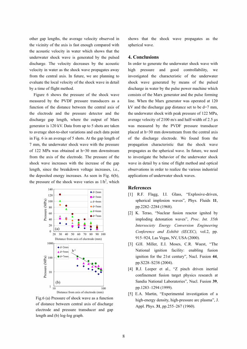
Figure 6 shows the pressure of the shock wave measured by the PVDF pressure transducers as a function of the distance between the central axis of the electrode and the pressure detector and the discharge gap length, where the output of Marx generator is 120 kV. Data from up to 5 shots are taken to average shot-to-shot variations and each data point in Fig. 6 is an average of 5 shots. At the gap length of 7 mm, the underwater shock wave with the pressure of 122 MPa was obtained at h=30 mm downstream from the axis of the electrode. The pressure of the shock wave increases with the increase of the gap length, since the breakdown voltage increases, i.e., the deposited energy increases. As seen in Fig. 6(b), the pressure of the shock wave varies as 1/h2, which
shows that the shock wave propagates as the spherical wave.
4. Conclusions In order to generate the underwater shock wave with high pressure and good controllability, we investigated the characteristic of the underwater shock wave generated by means of the pulsed discharge in water by the pulse power machine which consists of the Marx generator and the pulse forming line. When the Marx generator was operated at 120 kV and the discharge gap distance set to be d=7 mm, the underwater shock with peak pressure of 122 MPa, average velocity of 2100 m/s and half-width of 2.5 �swas measured by the PVDF pressure transducer placed at h=30 mm downstream from the central axis of the discharge electrode. We found from the propagation characteristic that the shock wave propagates as the spherical wave. In future, we need to investigate the behavior of the underwater shock wave in detail by a time of flight method and optical observations in order to realize the various industrial applications of underwater shock waves.
References [1] R.F. Flagg, I.I. Glass, “Explosive-driven,
spherical implosion waves”, Phys. Fluids 11,pp.2282–2284 (1968).
[2] K. Terao, “Nuclear fusion reactor ignited by imploding detonation waves”, Proc. Int. 35th Intersociety Energy Conversion Engineering Conference and Exhibit (IECEC), vol.2, pp. 915–924, Las Vegas, NV, USA (2000).
[3] G.H. Miller, E.I. Moses, C.R. Wuest, “The National ignition facility: enabling fusion ignition for the 21st century”, Nucl. Fusion 44,pp.S228–S238 (2004).
[4] R.J. Leeper et al., “Z pinch driven inertial confinement fusion target physics research at Sandia National Laboratories”, Nucl. Fusion 39,pp.1283–1294 (1999).
[5] E.A. Martin, “Experimental investigation of a high-energy density, high-pressure arc plasma”, J. Appl. Phys. 31, pp.255–267 (1960).
d=2mm
d=3mm
d=4mm
d=5mm
d=6mm
d=7mm
Pres
sure
(MPa
)
20 30 40 50 60 70 80 90 100Distance from axis of electrode (mm)
0
20
40
60
80
100
120
140
(a)
d=2mmd=5mm
d=7mm
10 100
Pres
sure
(MPa
)
Distance from axis of electrode (mm)
(b)1
10
100
1000
h-2
Fig.6 (a) Pressure of shock wave as a function of distance between central axis of discharge electrode and pressure transducer and gap length and (b) log-log graph.
88
Discharge Phenomena in Supercritical Carbon Dioxide
Takeshi Ihara, Tsuyoshi, Kiyan, Sunao Katsuki, Masanori Hara and Hidenori Akiyama
Graduate School of Science and Technology, Kumamoto University
ABSTRACT Pulsed streamers in highly pressurized carbon dioxide, including supercritical state were observed using the Schlieren method. The medium temperature and pressure were set to T= 305 K and P= 7.5, 8.0 MPa, respectively. The gap was a needle-to-plane: the gap length and the tip radius were d=7 and 1 mm and 5 �m, respectively. Pulse voltages of positive/negative polarity generated by a magnetic pulse compression generator were applied to a needle electrode. The main results obtained can be summarized as follows: Positive streamers in a supercritical state are branched tree-like, associated with shock waves of spherical and cylindrical shapes; their average development velocity is in order of 60 km/s. Conversely, the negative corona shape in a supercritical state, a spherical shape without branches, differs greatly from the positive one. The spherical shock wave started from the needle tip at the corona onset. Appearances of positive/ negative discharge obviously differ.
KeywordsKey Words: Pulse streamer, supercritical fluids, carbon dioxide, polarity effect
1. Introduction Discharge plasma in supercritical fluids has attracted much attention in new discharge plasma sciences [1]-[2]. Supercritical fluids (SCFs) exist at a state that is heated and pressurized above a critical point (fig.1). SCFs have very unique characteristics as an intermediate medium between a gas and a liquid. Supercritical carbon dioxide (scCO2) in particularly has been actively used as a generation field of discharge plasma.
Breakdown characteristics in scCO2 have been investigated in previous research. T. Kiyan et al. have reported polarity effects on DC breakdown in needle-to-plane electrode geometry from high pressurized gas state to supercritical condition [1]. The results show that, only for negative polarity discharge and not for positive, breakdown voltage in sub- and supercritical state increased due to the occurrence of corona discharge before breakdown. The corona discharge caused relaxation of the electric field at the needle tip. T. Ihara et al. have reported on observation
of pulsed streamer discharge in scCO2[2]. The report
for the first time indicated the appearance of streamers; these streamers had many branches, and spherical shock waves were confirmed along streamer channels.
This paper investigates polarity effects on pulsed pre-breakdown phenomena in supercritical using the laser Schlieren method.
Fig. 1 Phase diagram of CO2
99
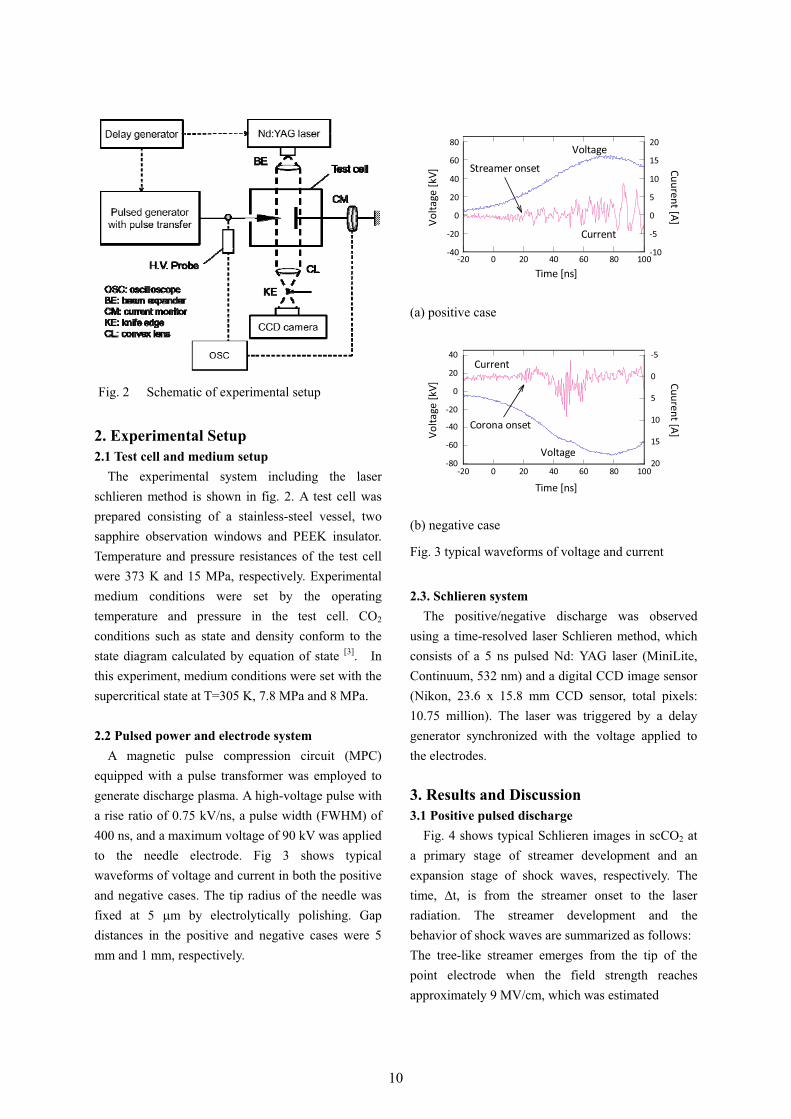
Fig. 2 Schematic of experimental setup
2. Experimental Setup 2.1 Test cell and medium setup
The experimental system including the laser schlieren method is shown in fig. 2. A test cell was prepared consisting of a stainless-steel vessel, two sapphire observation windows and PEEK insulator. Temperature and pressure resistances of the test cell were 373 K and 15 MPa, respectively. Experimental medium conditions were set by the operating temperature and pressure in the test cell. CO2
conditions such as state and density conform to the state diagram calculated by equation of state [3]. In this experiment, medium conditions were set with the supercritical state at T=305 K, 7.8 MPa and 8 MPa.
2.2 Pulsed power and electrode system A magnetic pulse compression circuit (MPC)
equipped with a pulse transformer was employed to generate discharge plasma. A high-voltage pulse with a rise ratio of 0.75 kV/ns, a pulse width (FWHM) of 400 ns, and a maximum voltage of 90 kV was applied to the needle electrode. Fig 3 shows typical waveforms of voltage and current in both the positive and negative cases. The tip radius of the needle was fixed at 5 �m by electrolytically polishing. Gap distances in the positive and negative cases were 5 mm and 1 mm, respectively.
�40
�20
0
20
40
60
80
�10
�5
0
5
10
15
20
�20 0 20 40 60 80 100
Volta
ge�[k
V]
Cuurent�[A]
Time�[ns]
Voltage
Current
Streamer�onset
(a) positive case
�80
�60
�40
�20
0
20
40 �5
0
5
10
15
20�20 0 20 40 60 80 100
Volta
ge�[k
V]
Cuurent�[A]
Time�[ns]
Voltage
Current
Corona�onset
(b) negative case
Fig. 3 typical waveforms of voltage and current
2.3. Schlieren system The positive/negative discharge was observed
using a time-resolved laser Schlieren method, which consists of a 5 ns pulsed Nd: YAG laser (MiniLite, Continuum, 532 nm) and a digital CCD image sensor (Nikon, 23.6 x 15.8 mm CCD sensor, total pixels: 10.75 million). The laser was triggered by a delay generator synchronized with the voltage applied to the electrodes.
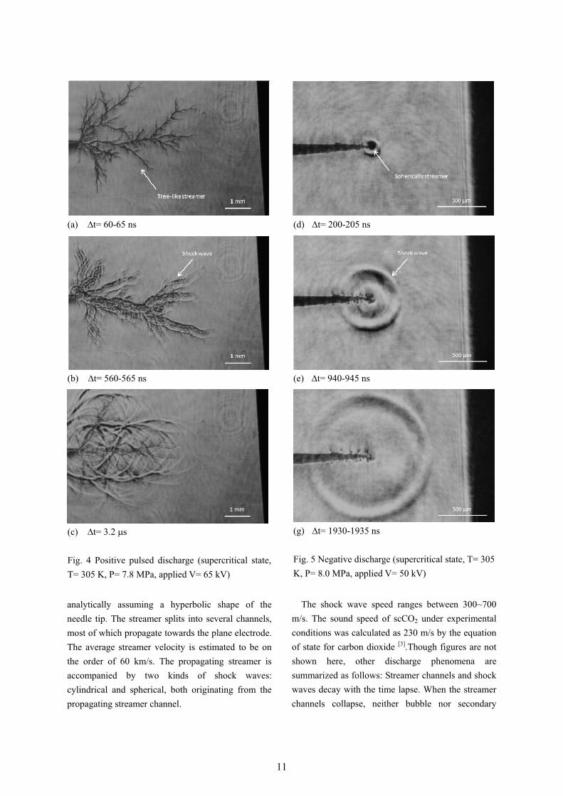
3. Results and Discussion 3.1 Positive pulsed discharge
Fig. 4 shows typical Schlieren images in scCO2 at a primary stage of streamer development and an expansion stage of shock waves, respectively. The time, �t, is from the streamer onset to the laser radiation. The streamer development and the behavior of shock waves are summarized as follows: The tree-like streamer emerges from the tip of the point electrode when the field strength reaches approximately 9 MV/cm, which was estimated
1010
(a) �t= 60-65 ns
(b) �t= 560-565 ns
(c) �t= 3.2 �s
Fig. 4 Positive pulsed discharge (supercritical state, T= 305 K, P= 7.8 MPa, applied V= 65 kV)
analytically assuming a hyperbolic shape of the needle tip. The streamer splits into several channels, most of which propagate towards the plane electrode. The average streamer velocity is estimated to be on the order of 60 km/s. The propagating streamer is accompanied by two kinds of shock waves: cylindrical and spherical, both originating from the propagating streamer channel.
(d) �t= 200-205 ns
(e) �t= 940-945 ns
(g) �t= 1930-1935 ns
Fig. 5 Negative discharge (supercritical state, T= 305 K, P= 8.0 MPa, applied V= 50 kV)
The shock wave speed ranges between 300~700 m/s. The sound speed of scCO2 under experimental conditions was calculated as 230 m/s by the equation of state for carbon dioxide [3].Though figures are not shown here, other discharge phenomena are summarized as follows: Streamer channels and shock waves decay with the time lapse. When the streamer channels collapse, neither bubble nor secondary
1111
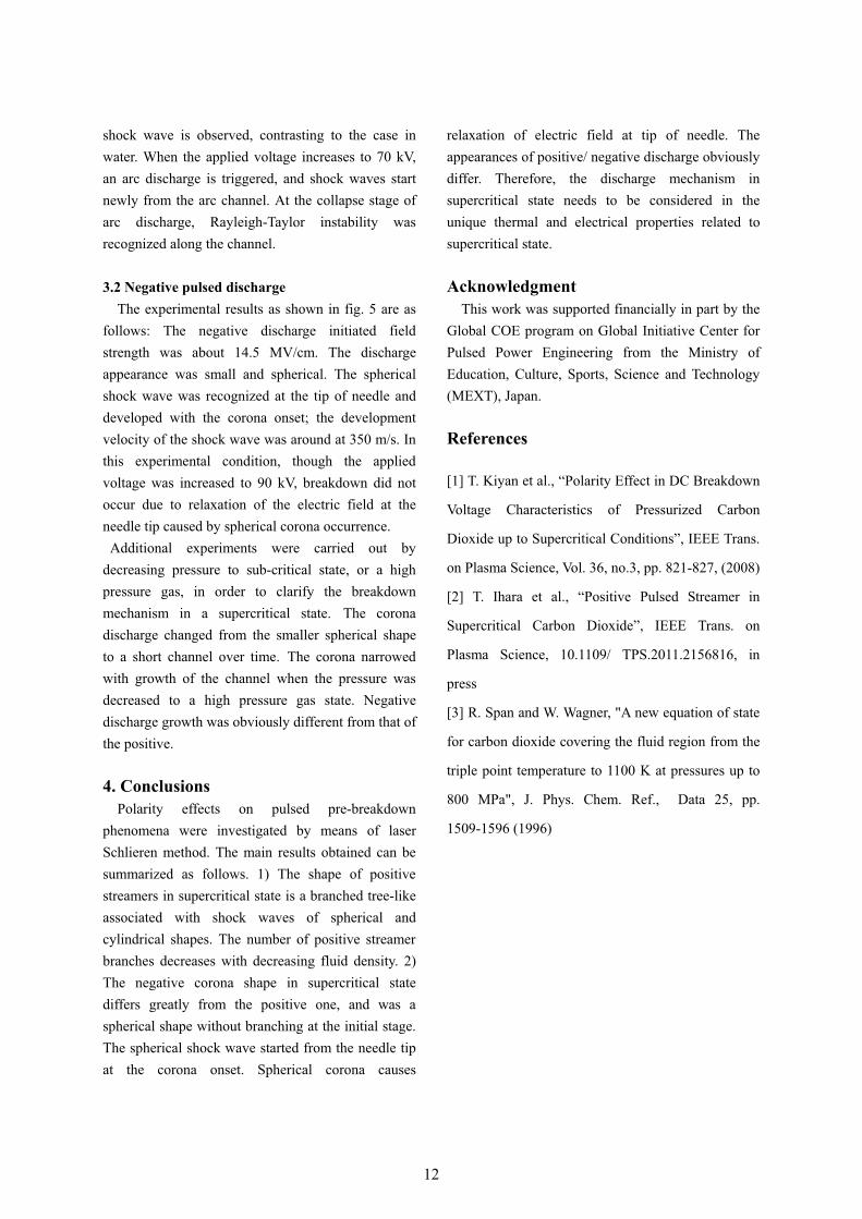
shock wave is observed, contrasting to the case in water. When the applied voltage increases to 70 kV, an arc discharge is triggered, and shock waves start newly from the arc channel. At the collapse stage of arc discharge, Rayleigh-Taylor instability was recognized along the channel.
3.2 Negative pulsed discharge The experimental results as shown in fig. 5 are as
follows: The negative discharge initiated field strength was about 14.5 MV/cm. The discharge appearance was small and spherical. The spherical shock wave was recognized at the tip of needle and developed with the corona onset; the development velocity of the shock wave was around at 350 m/s. In this experimental condition, though the applied voltage was increased to 90 kV, breakdown did not occur due to relaxation of the electric field at the needle tip caused by spherical corona occurrence. Additional experiments were carried out by
decreasing pressure to sub-critical state, or a high pressure gas, in order to clarify the breakdown mechanism in a supercritical state. The corona discharge changed from the smaller spherical shape to a short channel over time. The corona narrowed with growth of the channel when the pressure was decreased to a high pressure gas state. Negative discharge growth was obviously different from that of the positive.
4. Conclusions Polarity effects on pulsed pre-breakdown phenomena were investigated by means of laser Schlieren method. The main results obtained can be summarized as follows. 1) The shape of positive streamers in supercritical state is a branched tree-like associated with shock waves of spherical and cylindrical shapes. The number of positive streamer branches decreases with decreasing fluid density. 2) The negative corona shape in supercritical state differs greatly from the positive one, and was a spherical shape without branching at the initial stage. The spherical shock wave started from the needle tip at the corona onset. Spherical corona causes
relaxation of electric field at tip of needle. The appearances of positive/ negative discharge obviously differ. Therefore, the discharge mechanism in supercritical state needs to be considered in the unique thermal and electrical properties related to supercritical state.
Acknowledgment This work was supported financially in part by the Global COE program on Global Initiative Center for Pulsed Power Engineering from the Ministry of Education, Culture, Sports, Science and Technology (MEXT), Japan.
References
[1] T. Kiyan et al., “Polarity Effect in DC Breakdown
Voltage Characteristics of Pressurized Carbon
Dioxide up to Supercritical Conditions”, IEEE Trans.
on Plasma Science, Vol. 36, no.3, pp. 821-827, (2008)
[2] T. Ihara et al., “Positive Pulsed Streamer in
Supercritical Carbon Dioxide”, IEEE Trans. on
Plasma Science, 10.1109/ TPS.2011.2156816, in
press
[3] R. Span and W. Wagner, "A new equation of state
for carbon dioxide covering the fluid region from the
triple point temperature to 1100 K at pressures up to
800 MPa", J. Phys. Chem. Ref., Data 25, pp.
1509-1596 (1996)
1212
Production of Metal Contained Carbon Plasma Using Shunting Arc Discharge for Composite Film Preparation
H. Aoki, K. Takahashi and K. Takaki
Iwate University, 4-3-5 Ueda, Morioka, Iwate 020-8551, JAPAN
ABSTRACT Nitrogen and titanium contained plasmas were induced by a carbon shunting arc discharge. The carbon shunting arc was generated using a carbon rod which was held vertically between a pair of titanium plane electrodes. The titanium ions were supplied from the titanium plane electrodes during the shunting arc discharge. The nitrogen gas was injected into the vicinity of the carbon rod to produce nitrogen contained plasmas. It was confirmed from a spectroscopic observation that the produced plasma contained carbon and titanium ions without nitrogen injection. The spectra of nitrogen species were also confirmed at 10 Pa nitrogen gas injected into the discharge chamber. The electron density was measured using a double probe and was obtained as 1018 m-3 orders.
Keywords
PBII&D, DLC, Shunting arc, Arc discharge, Ion source, Ion density, Double probe.
1. Introduction A shunting arc is a pulsed plasma source for solid-state materials such as titanium, tungsten, silicon and carbon [1-2]. The shunting arc is ignited by self-heating of the rod material to increase vapor pressure and/or emit thermo electrons around the material, which is connected to a current source such as a capacitor [3]. Since the shunting arc system consists of simple components, it has a potential to be a cost-effective technology. Moreover, the shunting arc can be easily generated in a wide gas pressure range from vacuum to atmospheric pressure by evaporation from a rod heated by a pulse current [4]. Accordingly, the shunting arc is a promising method to prepare droplet-free films [5].
Diamond-like carbon (DLC) based composite films have many superior properties such as high hardness and optical characteristics and are used in many industrial applications for surface modification. DLC films can be prepared using the shunting arc discharge employing a carbon rod as a solid material [5]. DLC-based composite films can also be prepared
using the carbon shunting arc with addition of reactive gases [6-7]. For example, a nitrogen-containing DLC film is prepared using a magnetically driven carbon shunting arc in nitrogen gas [7].
DLC films containing metals such as titanium and tungsten stir up interest in various application fields owing to their excellent tribological properties, high electrical conductivity, and so on. These superior properties are suitable for many kinds of sensors such as electro-catalytic sensors. The titanium-containing DLC film with a few hundreds of nanometer thickness is prepared as a low friction coating using the sputtering procedures.
The shunting arc discharge in various electrode materials may be capable of producing individual composite films. The titanium-containing DLC film was prepared using carbon shunting arc discharge with titanium rail electrodes [8]. It was confirmed based on spectroscopic measurements that the shunting arc plasma contained titanium and carbon ions which were extracted by negative pulse voltage.
1313
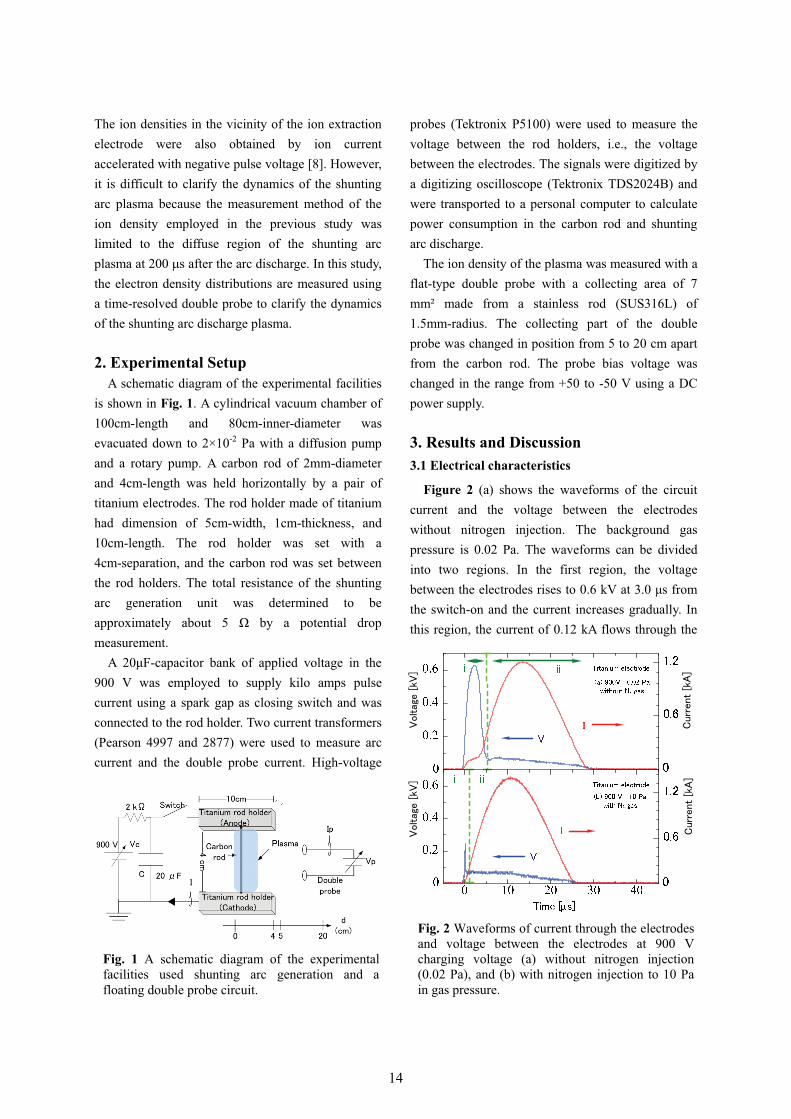
The ion densities in the vicinity of the ion extraction electrode were also obtained by ion current accelerated with negative pulse voltage [8]. However, it is difficult to clarify the dynamics of the shunting arc plasma because the measurement method of the ion density employed in the previous study was limited to the diffuse region of the shunting arc plasma at 200 �s after the arc discharge. In this study, the electron density distributions are measured using a time-resolved double probe to clarify the dynamics of the shunting arc discharge plasma. 2. Experimental Setup A schematic diagram of the experimental facilities is shown in Fig. 1. A cylindrical vacuum chamber of 100cm-length and 80cm-inner-diameter was evacuated down to 2×10⁻² Pa with a diffusion pump and a rotary pump. A carbon rod of 2mm-diameter and 4cm-length was held horizontally by a pair of titanium electrodes. The rod holder made of titanium had dimension of 5cm-width, 1cm-thickness, and 10cm-length. The rod holder was set with a 4cm-separation, and the carbon rod was set between the rod holders. The total resistance of the shunting arc generation unit was determined to be approximately about 5 � by a potential drop measurement.
A 20�F-capacitor bank of applied voltage in the 900 V was employed to supply kilo amps pulse current using a spark gap as closing switch and was connected to the rod holder. Two current transformers (Pearson 4997 and 2877) were used to measure arc current and the double probe current. High-voltage
probes (Tektronix P5100) were used to measure the voltage between the rod holders, i.e., the voltage between the electrodes. The signals were digitized by a digitizing oscilloscope (Tektronix TDS2024B) and were transported to a personal computer to calculate power consumption in the carbon rod and shunting arc discharge.
The ion density of the plasma was measured with a flat-type double probe with a collecting area of 7 mm² made from a stainless rod (SUS316L) of 1.5mm-radius. The collecting part of the double probe was changed in position from 5 to 20 cm apart from the carbon rod. The probe bias voltage was changed in the range from +50 to -50 V using a DC power supply. 3. Results and Discussion 3.1 Electrical characteristics
Figure 2 (a) shows the waveforms of the circuit current and the voltage between the electrodes without nitrogen injection. The background gas pressure is 0.02 Pa. The waveforms can be divided into two regions. In the first region, the voltage between the electrodes rises to 0.6 kV at 3.0 �s from the switch-on and the current increases gradually. In this region, the current of 0.12 kA flows through the
����
Fig. 1 A schematic diagram of the experimental facilities used shunting arc generation and a floating double probe circuit.
���� ����
�
���� ������
���� ����
�
���� ������
Fig. 2 Waveforms of current through the electrodes and voltage between the electrodes at 900 V charging voltage (a) without nitrogen injection (0.02 Pa), and (b) with nitrogen injection to 10 Pa in gas pressure.
1414
rod. These current values almost agree with those estimated based on Ohm’s law (=600V/5�). Therefore this phase indicates the current flows through the rod and the rod temperature rises with Ohmic heating process.
In the second region, the voltage abruptly decreases 6.0 �s after switching on the closing gap switch and the abrupt decrease of voltage is accompanied by an abrupt increase in current. These rapid changes in voltage and current indicate the initiation of the shunting arc. The arc current is sinusoidal with duration of about 35 �s, and its peak current is about 1.1 kV, 20 �s after switch-on. This is due to LC oscillation from the capacitor and the inductance of the wiring of the present shunting arc generation system. The minimum resistance of the arc discharge can be estimated from the current and the voltage waveforms and is obtained as 0.08 �.
Figure2 (b) shows the waveform of the circuit current and the voltage between the electrodes with nitrogen injection to 10 Pa in gas pressure. In the first region, the voltage between the carbon electrode rises to 0.5 kV in 1.0 �s. In this region, the current of about 0.05 kA flows through the rod. The arc current is sinusoidal with duration of approximately 25 �s, and its peak current is about 1.2 kV at 13 �s after the switch-on.
Figure 3 shows the heating energy to ignite the shunting arc and the onset voltage as a function of nitrogen gas pressure at 900 V charging voltage of
the capacitor. The heating energy and the onset voltage have U-shape characteristics in pressure range from 0.02 to 400 Pa. The heating energy decreases from 0.4 to 0.003 J with increasing gas pressure from 0.02 to 10 Pa in Paschen left region, and then increases to about 0.3 J with increasing gas pressure to 400 Pa. The discharge onset voltage decreases from 800 to 240 V with increasing gas pressure from 0.01 to 10 Pa, and then increases to about 800 V with increasing gas pressure to 400 Pa.
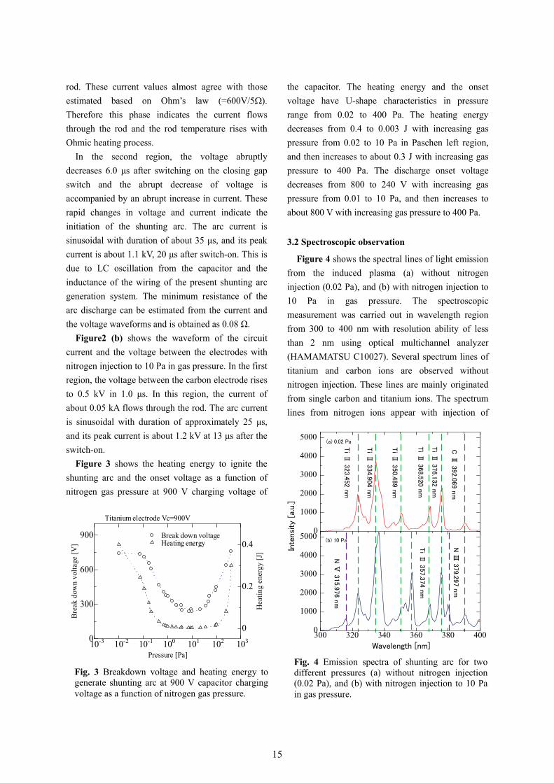
3.2 Spectroscopic observation
Figure 4 shows the spectral lines of light emission from the induced plasma (a) without nitrogen injection (0.02 Pa), and (b) with nitrogen injection to 10 Pa in gas pressure. The spectroscopic measurement was carried out in wavelength region from 300 to 400 nm with resolution ability of less than 2 nm using optical multichannel analyzer (HAMAMATSU C10027). Several spectrum lines of titanium and carbon ions are observed without nitrogen injection. These lines are mainly originated from single carbon and titanium ions. The spectrum lines from nitrogen ions appear with injection of
����
������
����
����
������
����
����
������
����
����
� ��������
����
�! �"�����
���
�����
���
�
0
1000
2000
3000
4000
5000
300 320 340 360 380 4000
1000
2000
3000
4000
5000
#� �$�%�������
&�' ��(�����
)�*
�"���
! ��
�
)�+
�!����!��
�
����
��!��!����
,�-������.�
,/-�"��.�
Fig. 4 Emission spectra of shunting arc for two different pressures (a) without nitrogen injection (0.02 Pa), and (b) with nitrogen injection to 10 Pa in gas pressure.
10-3 10-2 10-1 100 101 102 1030
300
600
900
0
0.2
0.4
Pressure [Pa]
Brea
k do
wn
volta
ge [V
]
Hea
ting
ener
gy [J
]
Titanium electrode Vc=900V
Break down voltage Heating energy
Fig. 3 Breakdown voltage and heating energy to generate shunting arc at 900 V capacitor charging voltage as a function of nitrogen gas pressure.
1515
nitrogen at 10 Pa in gas pressure. The lines from single carbon and titanium ions are also observed. Intensities of the light emission from titanium ions increase by injecting nitrogen gas owing to the increase of the arc current as shown in Fig. 2.
3.3 Double probe measurement
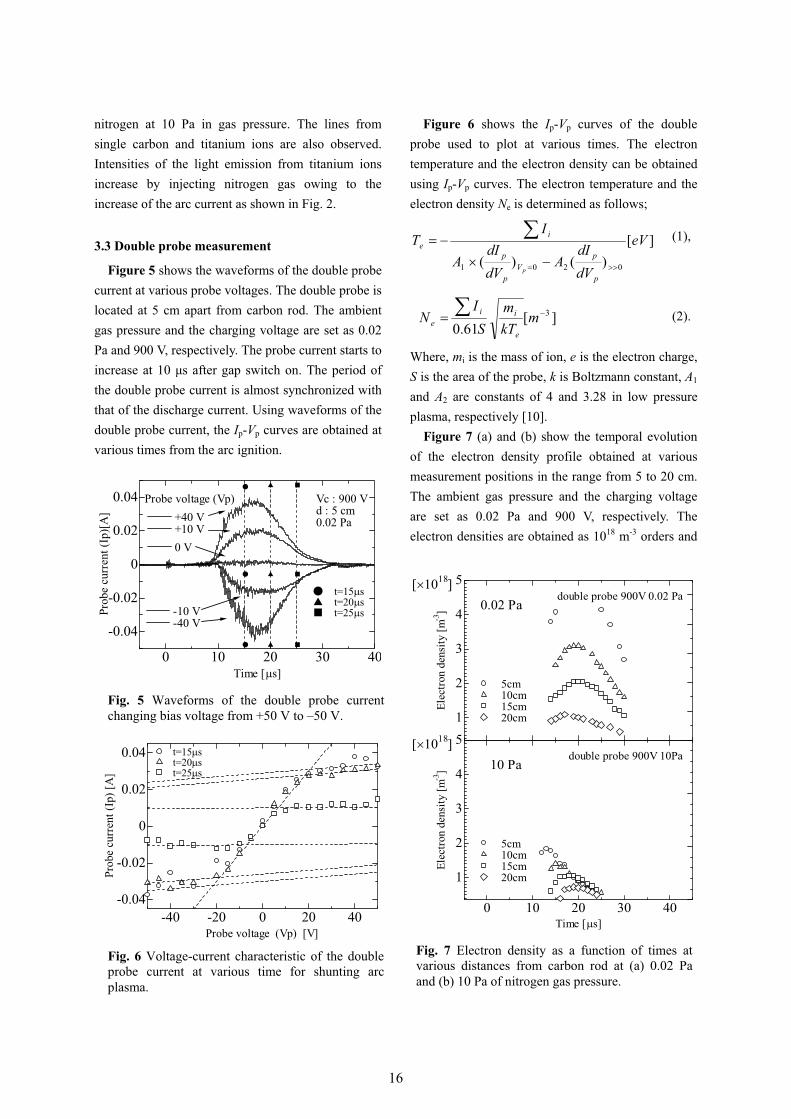
Figure 5 shows the waveforms of the double probe current at various probe voltages. The double probe is located at 5 cm apart from carbon rod. The ambient gas pressure and the charging voltage are set as 0.02 Pa and 900 V, respectively. The probe current starts to increase at 10 �s after gap switch on. The period of the double probe current is almost synchronized with that of the discharge current. Using waveforms of the double probe current, the Ip-Vp curves are obtained at various times from the arc ignition.
Figure 6 shows the Ip-Vp curves of the double probe used to plot at various times. The electron temperature and the electron density can be obtained using Ip-Vp curves. The electron temperature and the electron density Ne is determined as follows;
][)()( 0201
eV
dVdI
AdVdI
A
IT
p
pV
p
p
ie
p ��� ��� (1),
][61.0
3�� mkTm
SI
Ne
iie � � � (2).
Where, mi is the mass of ion, e is the electron charge, S is the area of the probe, k is Boltzmann constant, A1
and A2 are constants of 4 and 3.28 in low pressure plasma, respectively [10].
Figure 7 (a) and (b) show the temporal evolution of the electron density profile obtained at various measurement positions in the range from 5 to 20 cm. The ambient gas pressure and the charging voltage are set as 0.02 Pa and 900 V, respectively. The electron densities are obtained as 1018 m-3 orders and
0 10 20 30 40
-0.04
-0.02
0
0.02
0.04
0 V
Vc : 900 Vd : 5 cm0.02 Pa
Prob
e cu
rren
t (Ip
)[A
]
Time [�s]
-10 V -40 V
+40 V +10 V
� � �
�
�
�
� �
�
��t=15�s��t=20�s��t=25�s
Probe voltage (Vp)
Fig. 5 Waveforms of the double probe current changing bias voltage from +50 V to –50 V.
-40 -20 0 20 40-0.04
-0.02
0
0.02
0.04 t=15�s t=20�s t=25�s
Probe voltage (Vp) [V]
Prob
e cu
rren
t (Ip
) [A
]
Fig. 6 Voltage-current characteristic of the double probe current at various time for shunting arc plasma.
1
2
3
4
5[1018]
5cm 10cm 15cm 20cm
Elec
tron
dens
ity [m
-3]
double probe 900V 0.02 Pa0.02 Pa
0 10 20 30 40
1
2
3
4
5[1018]
Elec
tron
dens
ity [m
-3]
Time [�s]
5cm 10cm 15cm 20cm
double probe 900V 10Pa10 Pa
Fig. 7 Electron density as a function of times at various distances from carbon rod at (a) 0.02 Pa and (b) 10 Pa of nitrogen gas pressure.
1616
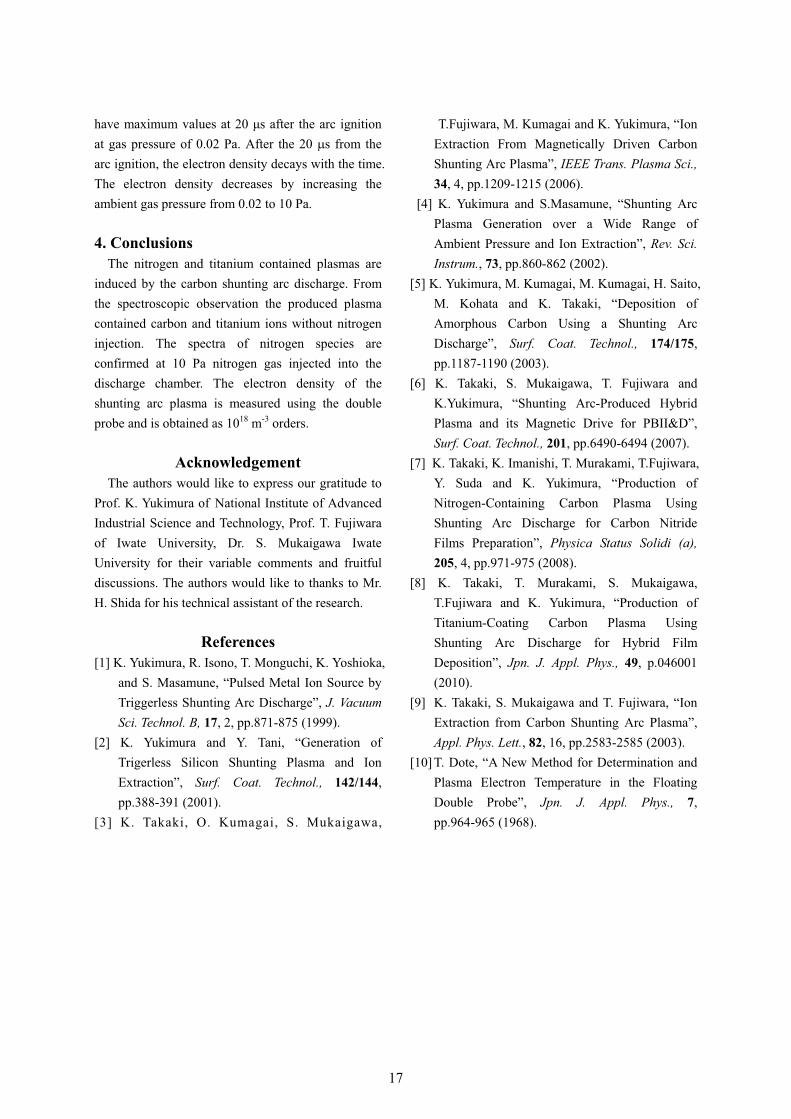
have maximum values at 20 �s after the arc ignition at gas pressure of 0.02 Pa. After the 20 �s from the arc ignition, the electron density decays with the time. The electron density decreases by increasing the ambient gas pressure from 0.02 to 10 Pa. 4. Conclusions
The nitrogen and titanium contained plasmas are induced by the carbon shunting arc discharge. From the spectroscopic observation the produced plasma contained carbon and titanium ions without nitrogen injection. The spectra of nitrogen species are confirmed at 10 Pa nitrogen gas injected into the discharge chamber. The electron density of the shunting arc plasma is measured using the double probe and is obtained as 1018 m-3 orders.
Acknowledgement
The authors would like to express our gratitude to Prof. K. Yukimura of National Institute of Advanced Industrial Science and Technology, Prof. T. Fujiwara of Iwate University, Dr. S. Mukaigawa Iwate University for their variable comments and fruitful discussions. The authors would like to thanks to Mr. H. Shida for his technical assistant of the research.
References
[1] K. Yukimura, R. Isono, T. Monguchi, K. Yoshioka, and S. Masamune, “Pulsed Metal Ion Source by Triggerless Shunting Arc Discharge”, J. Vacuum Sci. Technol. B, 17, 2, pp.871-875 (1999).
[2] K. Yukimura and Y. Tani, “Generation of Trigerless Silicon Shunting Plasma and Ion Extraction”, Surf. Coat. Technol., 142/144, pp.388-391 (2001).
[3] K. Takaki, O. Kumagai, S. Mukaigawa,
T.Fujiwara, M. Kumagai and K. Yukimura, “Ion Extraction From Magnetically Driven Carbon Shunting Arc Plasma”, IEEE Trans. Plasma Sci., 34, 4, pp.1209-1215 (2006).
[4] K. Yukimura and S.Masamune, “Shunting Arc Plasma Generation over a Wide Range of Ambient Pressure and Ion Extraction”, Rev. Sci. Instrum., 73, pp.860-862 (2002).
[5] K. Yukimura, M. Kumagai, M. Kumagai, H. Saito, M. Kohata and K. Takaki, “Deposition of Amorphous Carbon Using a Shunting Arc Discharge”, Surf. Coat. Technol., 174/175, pp.1187-1190 (2003).
[6] K. Takaki, S. Mukaigawa, T. Fujiwara and K.Yukimura, “Shunting Arc-Produced Hybrid Plasma and its Magnetic Drive for PBII&D”, Surf. Coat. Technol., 201, pp.6490-6494 (2007).
[7] K. Takaki, K. Imanishi, T. Murakami, T.Fujiwara, Y. Suda and K. Yukimura, “Production of Nitrogen-Containing Carbon Plasma Using Shunting Arc Discharge for Carbon Nitride Films Preparation”, Physica Status Solidi (a), 205, 4, pp.971-975 (2008).
[8] K. Takaki, T. Murakami, S. Mukaigawa, T.Fujiwara and K. Yukimura, “Production of Titanium-Coating Carbon Plasma Using Shunting Arc Discharge for Hybrid Film Deposition”, Jpn. J. Appl. Phys., 49, p.046001 (2010).
[9] K. Takaki, S. Mukaigawa and T. Fujiwara, “Ion Extraction from Carbon Shunting Arc Plasma”, Appl. Phys. Lett., 82, 16, pp.2583-2585 (2003).
[10] T. Dote, “A New Method for Determination and Plasma Electron Temperature in the Floating Double Probe”, Jpn. J. Appl. Phys., 7, pp.964-965 (1968).
1717
APPLICATION OF TRIBOLUMINESCENCE TO ROENTGEN DIAGNOSIS
Naoya TASHIRO and Seizo FURUYA
Saitama Institute of Technology, Fukaya 369-0293 JAPAN
ABSTRACT
Triboluminescence is a luminous phenomenon resulted from friction; for example, peeling scotch tape, breaking rock sugar with a hammer, peeling mica and so on. Triboluminescence is well known over 50 years but in 2008 UCLA group reported the radiation of x-ray region by triboluminescence in vacuum for the first time. UCLA group made an automatic machine which peels scotch tape. With a view to practical application of triboluminescence to roentgen diagnosis we made an automatic peeling machine similar to that of UCLA group. Replacing conventional x-ray tube with triboluminescence is very useful to roentgen diagnosis. First, we have confirmed the x-ray generation from triboluminescence using a filtered phosphor screen when the parameters such as the followings are changed; peeling speed, atmospheric pressure, variety of scotch tape, emission angle etc. Then in a similar way we have successfully measured the x-ray dose from triboluminescence using a potable dosemeter. It was found that the x-ray generation from triboluminescence has a directional property.
I. Introduction Triboluminescence is a luminous phenomenon
resulted from friction; for example, peeling scotch tape, breaking rock sugar with a hammer, peeling mica and so on. Triboluminescence is well known over 50 years but in 2008 UCLA group reported the radiation of x-ray region by triboluminescence in vacuum for the first time.1) UCLA group made an automatic machine which peels scotch tape. With a view to practical application of triboluminescence to roentgen diagnosis we made an automatic peeling machine similar to that of UCLA group. An x-ray tube for conventional roentgen diagnosis needs a high voltage power supply. In contrast, triboluminescence does not need it. So it is very useful for roentgen diagnosis to replace a conventional x-ray tube with triboluminescence.
In our previous report2), we have made an automatic peeling machine similar to that of UCLA group and have confirmed the visible light and x-ray emissions from the peeling tape. The visible light emission from peeling tape seems continuous by the naked eye but we have verified using a photomultiplier that the peeling tape emits light in pulses actually.
In this report, at first, we have confirmed the x-ray generation from triboluminescence using a filtered phosphor screen when the parameters such as the followings are changed; peeling speed, atmospheric pressure, variety of scotch tape, emission angle etc. Then in a similar way we have
successfully measured the x-ray dose from triboluminescence using a potable dosemeter. It was found that the x-ray generation from triboluminescence has a directional property.
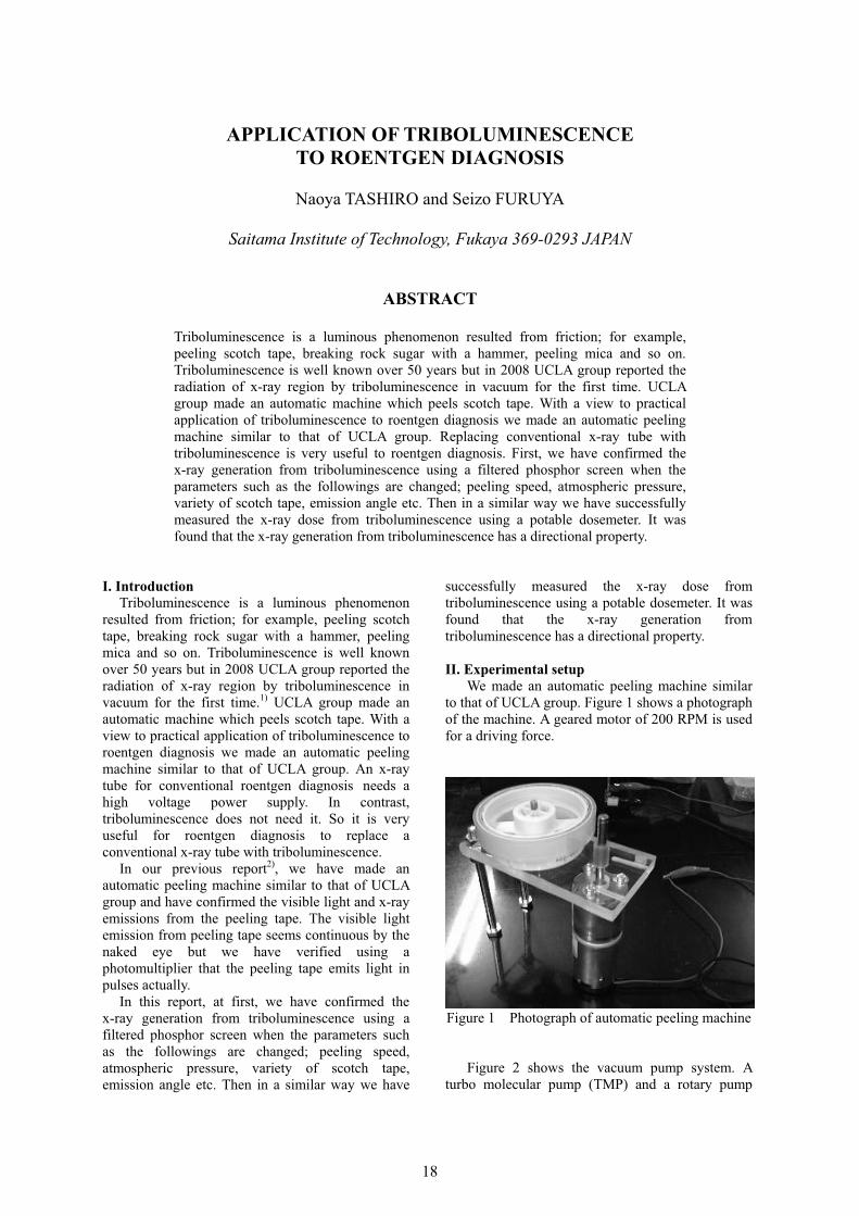
II. Experimental setup We made an automatic peeling machine similar to that of UCLA group. Figure 1 shows a photograph of the machine. A geared motor of 200 RPM is used for a driving force.
Figure 1 Photograph of automatic peeling machine
Figure 2 shows the vacuum pump system. A turbo molecular pump (TMP) and a rotary pump
1818
(RP1) are a pair (PFEIFFER VACUUM, Turbomolecular Drag Pumping Station TSH261 with DUO2.5). The pumping speed of RP1 is 2.5 m3/h and total pumping speed is 210 L/s. To enhance the pumping capability RP2 (SHINKU KIKO, GVD-135A, 135 L/m) is added.
Figure 2 Vacuum pump system
Figure 3 shows a photograph of the vacuum chamber. The inner diameter is 210.7 mm and the inner height is 200 mm.
Figure 3 Photograph of vacuum chamber
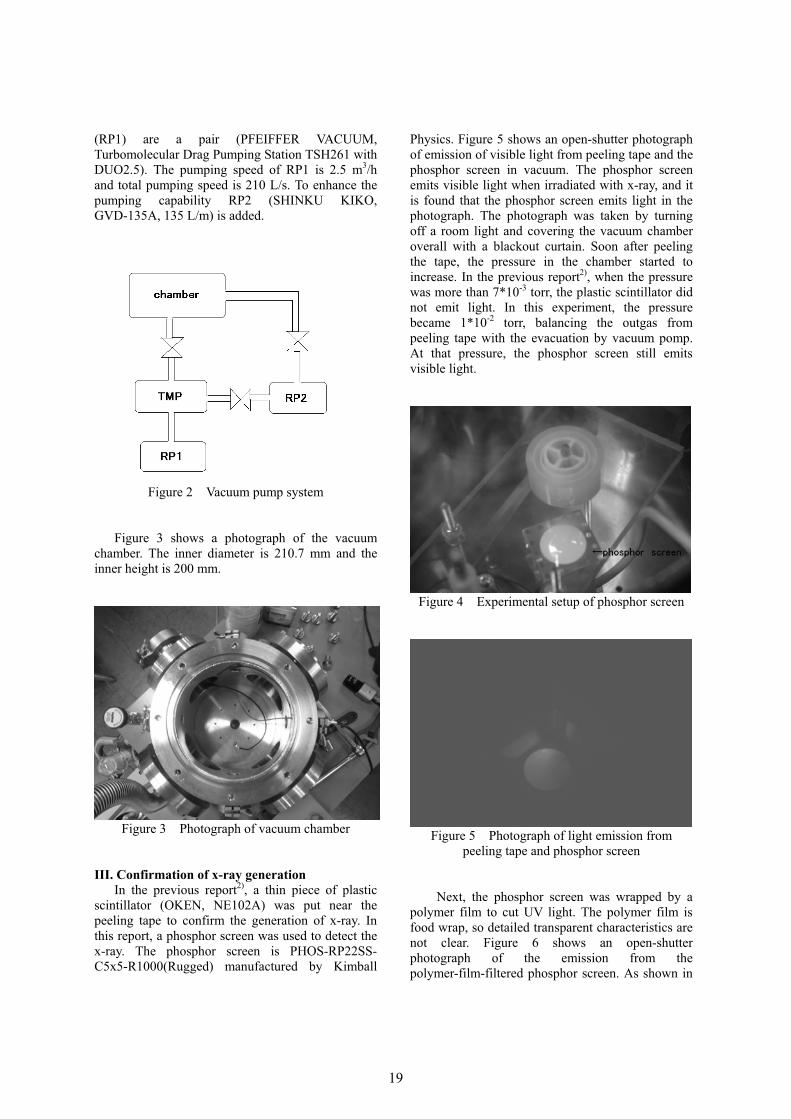
III. Confirmation of x-ray generation In the previous report2), a thin piece of plastic scintillator (OKEN, NE102A) was put near the peeling tape to confirm the generation of x-ray. In this report, a phosphor screen was used to detect the x-ray. The phosphor screen is PHOS-RP22SS- C5x5-R1000(Rugged) manufactured by Kimball
Physics. Figure 5 shows an open-shutter photograph of emission of visible light from peeling tape and the phosphor screen in vacuum. The phosphor screen emits visible light when irradiated with x-ray, and it is found that the phosphor screen emits light in the photograph. The photograph was taken by turning off a room light and covering the vacuum chamber overall with a blackout curtain. Soon after peeling the tape, the pressure in the chamber started to increase. In the previous report2), when the pressure was more than 7*10-3 torr, the plastic scintillator did not emit light. In this experiment, the pressure became 1*10-2 torr, balancing the outgas from peeling tape with the evacuation by vacuum pomp. At that pressure, the phosphor screen still emits visible light.
Figure 4 Experimental setup of phosphor screen
Figure 5 Photograph of light emission from peeling tape and phosphor screen
Next, the phosphor screen was wrapped by a polymer film to cut UV light. The polymer film is food wrap, so detailed transparent characteristics are not clear. Figure 6 shows an open-shutter photograph of the emission from the polymer-film-filtered phosphor screen. As shown in
1919

the figure, because the polymer film was not flat, the phosphor screen emitted light in stripes.
Figure 6 Photograph of emission from polymer-film-filtered phosphor screen
Figure 7 Experimental setup of aluminum foil
Figure 8 Photograph of emission from aluminum-foil-filtered phosphor screen
Finally, an aluminum foil was set between peeling tape and phosphor screen to cut visible and UV light. The experimental setup of the aluminum foil was shown in Figure 7, and Figure 8 shows an open-shutter photograph of the emission from the aluminum-foil-filtered phosphor screen. As shown in
Figure 8, because the size of aluminum foil is insufficient, the phosphor screen produced luminescence in semicircular shape due to stray light.
IV. Measurement of x-ray dose Figure 9 shows the experimental setup to
measure the x-ray dose of upward direction. The x-ray dose was measured using a portable dosemeter(ALOKA, PDM-117). Figure 10 shows the time variation of pressure and accumulated x-ray dose. The dotted lines in the figure are the data in the case that the initial pressure was 1.0*10-3 torr and the peeling speed is 0.6-1.2 cm/s. The x-ray dose of 1 �Sv was detected for 10-minute exposure. The broken lines are the experimental results in the case of 7.8*10-4 torr and 0.6-1.2 cm/s. When the initial pressure is low, the x-ray dose increases. When the peeling speed increases, the x-ray dose also increases? The continuous lines are the data in the case that the peeling speed is twice. The answer is no because the pressure rapidly increases.
Figure 9 Experimental setup to measure x-ray dose of upward direction
Figure 10 Time variation of pressure and accumulated x-ray dose
2020
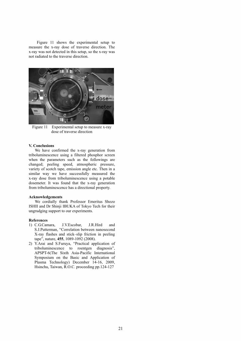
Figure 11 shows the experimental setup to measure the x-ray dose of traverse direction. The x-ray was not detected in this setup, so the x-ray was not radiated to the traverse direction.
Figure 11 Experimental setup to measure x-ray dose of traverse direction
V. Conclusions We have confirmed the x-ray generation from triboluminescence using a filtered phosphor screen when the parameters such as the followings are changed; peeling speed, atmospheric pressure, variety of scotch tape, emission angle etc. Then in a similar way we have successfully measured the x-ray dose from triboluminescence using a potable dosemeter. It was found that the x-ray generation from triboluminescence has a directional property.
Acknowledgements We cordially thank Professor Emeritus Shozo ISHII and Dr Shinji IBUKA of Tokyo Tech for their ungrudging support to our experiments.
References 1) C.G.Camara, J.V.Escobar, J.R.Hird and
S.J.Putterman, “Correlation between nanosecond X-ray flashes and stick–slip friction in peeling tape”, nature, 455, 1089-1092 (2008).
2) Y.Arai and S.Furuya, “Practical application of triboluminescence to roentgen diagnosis”, APSPT-6(The Sixth Asia-Pacific International Symposium on the Basic and Application of Plasma Technology) December 14-16, 2009, Hsinchu, Taiwan, R.O.C. proceeding pp.124-127
2121
Laser Target using Continuous Supersonic Jet
Yujin Ogata, Kazumasa Takahashi, Hajime Kuwabara1, Mitsuo Nakajima, and Kazuhiko Horioka∗Department of Energy Sciences, Tokyo Institute of Technology,
Nagatsuta 4259, Midori-ku, Yokohama, 226-8502, Japan1Yokohama Engineering Center, IHI Corporation, 1,
Shin-nakaharacho, Isago-ku, Yokohama, 235-8501, Japan
For an extreme ultraviolet (EUV) light source, Sn plasmas, which can produce a strong radiationwith high conversion efficiency at 13.5nm, attract attention. The purpose of this study is to establishtechnology to form and recover a tin vapor supersonic jet in vacuum and to make clear the interactionbetween the supersonic free jet and an incident laser experimentally. In order to make the tin vapor,a tantalum crucible is inductively heated up and the radiation loss is compared with the input energy.In future, we increase the number of shields and heat the tantalum crucible to the boiling point.We observe the density gradient of vapor jet emitted from a supersonic nozzle by shadowgraph. Weare planning to make a study on the interaction process between laser and the free jet.
Keywords: EUV, Debris, Laser-produced plasma, Tin, Supersonic free jet
I. INTRODUCTION
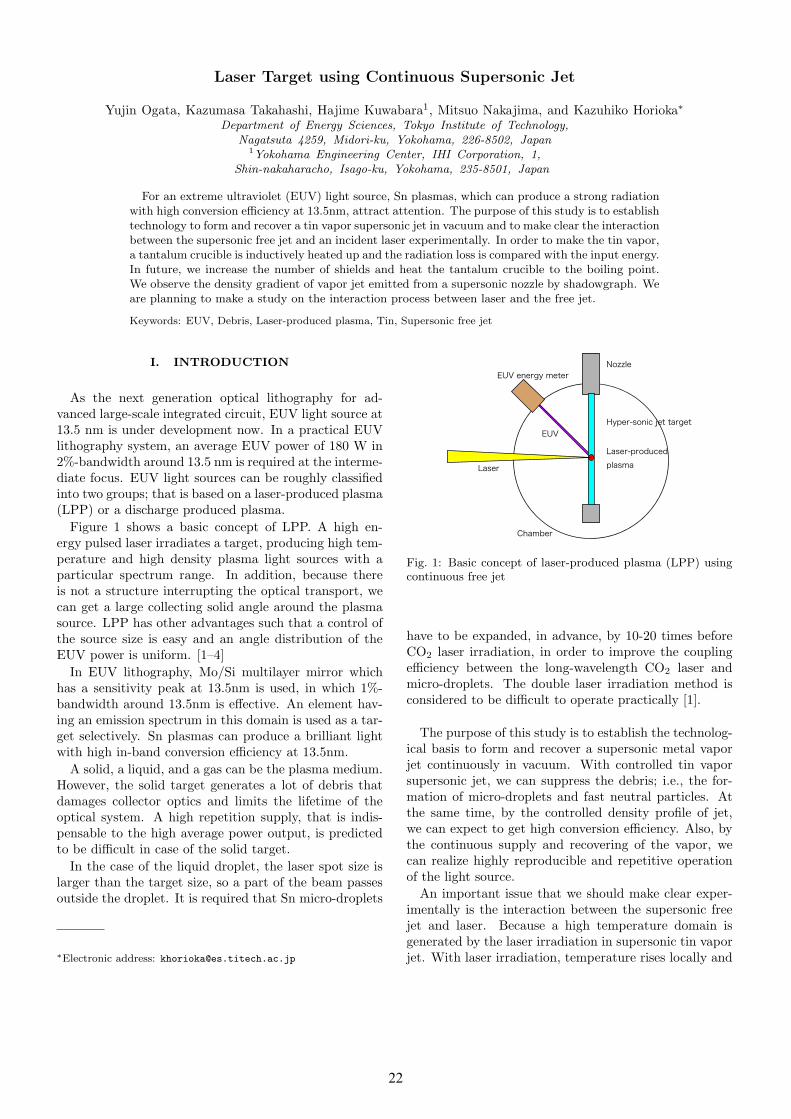
As the next generation optical lithography for ad-vanced large-scale integrated circuit, EUV light source at13.5 nm is under development now. In a practical EUVlithography system, an average EUV power of 180 W in2%-bandwidth around 13.5 nm is required at the interme-diate focus. EUV light sources can be roughly classifiedinto two groups; that is based on a laser-produced plasma(LPP) or a discharge produced plasma.
Figure 1 shows a basic concept of LPP. A high en-ergy pulsed laser irradiates a target, producing high tem-perature and high density plasma light sources with aparticular spectrum range. In addition, because thereis not a structure interrupting the optical transport, wecan get a large collecting solid angle around the plasmasource. LPP has other advantages such that a control ofthe source size is easy and an angle distribution of theEUV power is uniform. [1–4]
In EUV lithography, Mo/Si multilayer mirror whichhas a sensitivity peak at 13.5nm is used, in which 1%-bandwidth around 13.5nm is effective. An element hav-ing an emission spectrum in this domain is used as a tar-get selectively. Sn plasmas can produce a brilliant lightwith high in-band conversion efficiency at 13.5nm.
A solid, a liquid, and a gas can be the plasma medium.However, the solid target generates a lot of debris thatdamages collector optics and limits the lifetime of theoptical system. A high repetition supply, that is indis-pensable to the high average power output, is predictedto be difficult in case of the solid target.
In the case of the liquid droplet, the laser spot size islarger than the target size, so a part of the beam passesoutside the droplet. It is required that Sn micro-droplets
∗Electronic address: [email protected]
Nozzle
Hyper-sonic jet target
Laser-producedplasma
EUV
EUV energy meter
Laser
Chamber
Fig. 1: Basic concept of laser-produced plasma (LPP) usingcontinuous free jet
have to be expanded, in advance, by 10-20 times beforeCO2 laser irradiation, in order to improve the couplingefficiency between the long-wavelength CO2 laser andmicro-droplets. The double laser irradiation method isconsidered to be difficult to operate practically [1].
The purpose of this study is to establish the technolog-ical basis to form and recover a supersonic metal vaporjet continuously in vacuum. With controlled tin vaporsupersonic jet, we can suppress the debris; i.e., the for-mation of micro-droplets and fast neutral particles. Atthe same time, by the controlled density profile of jet,we can expect to get high conversion efficiency. Also, bythe continuous supply and recovering of the vapor, wecan realize highly reproducible and repetitive operationof the light source.
An important issue that we should make clear exper-imentally is the interaction between the supersonic freejet and laser. Because a high temperature domain isgenerated by the laser irradiation in supersonic tin vaporjet. With laser irradiation, temperature rises locally and
2222
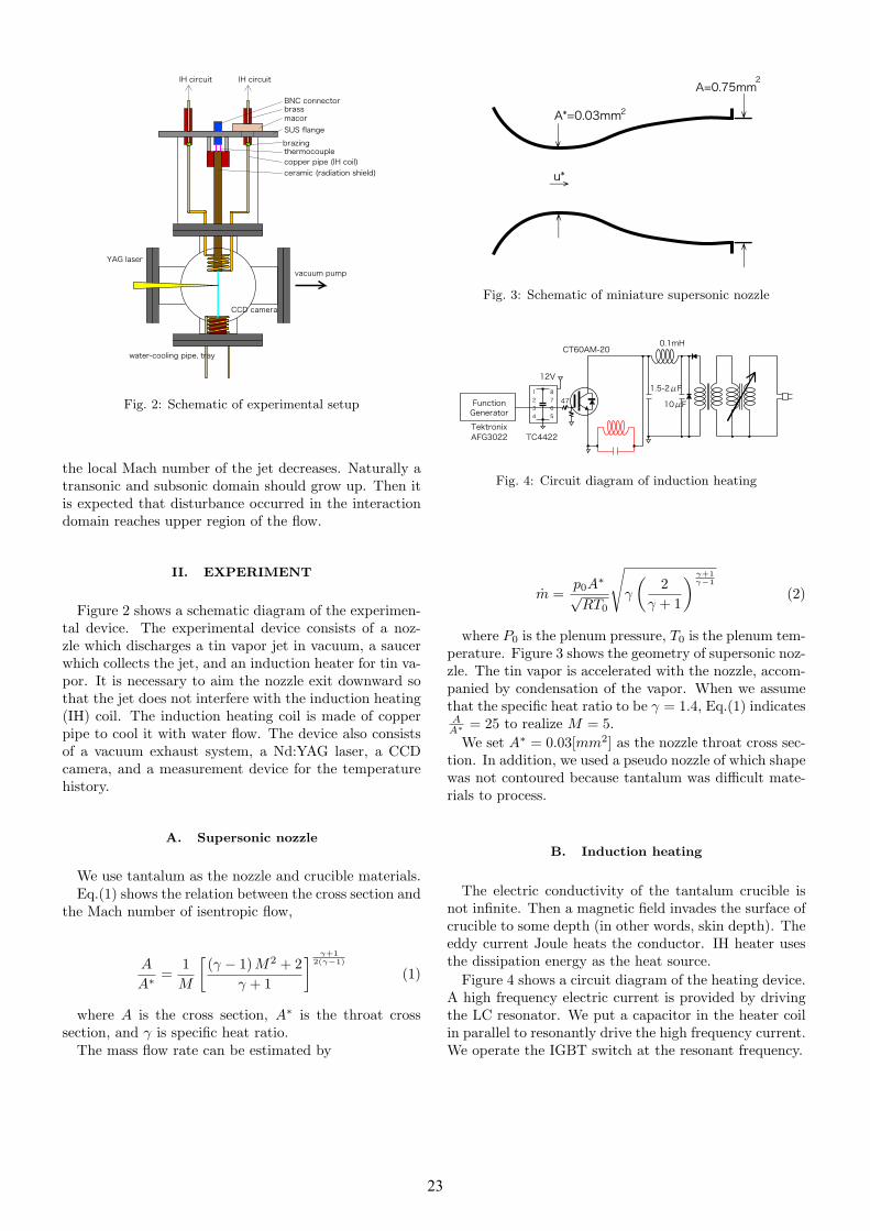
YAG laser
vacuum pump
water-cooling pipe, tray
CCD camera
BNC connector
copper pipe (IH coil)
brass
brazing
macor
ceramic (radiation shield)
thermocouple
SUS flange
IH circuit IH circuit
Fig. 2: Schematic of experimental setup
the local Mach number of the jet decreases. Naturally atransonic and subsonic domain should grow up. Then itis expected that disturbance occurred in the interactiondomain reaches upper region of the flow.
II. EXPERIMENT
Figure 2 shows a schematic diagram of the experimen-tal device. The experimental device consists of a noz-zle which discharges a tin vapor jet in vacuum, a saucerwhich collects the jet, and an induction heater for tin va-por. It is necessary to aim the nozzle exit downward sothat the jet does not interfere with the induction heating(IH) coil. The induction heating coil is made of copperpipe to cool it with water flow. The device also consistsof a vacuum exhaust system, a Nd:YAG laser, a CCDcamera, and a measurement device for the temperaturehistory.
A. Supersonic nozzle
We use tantalum as the nozzle and crucible materials.Eq.(1) shows the relation between the cross section and
the Mach number of isentropic flow,
A
A∗ =1M
[(γ − 1) M2 + 2
γ + 1
] γ+12(γ−1)
(1)
where A is the cross section, A∗ is the throat crosssection, and γ is specific heat ratio.
The mass flow rate can be estimated by
→u*
↓
↓↓
↓2
A=0.75mm2
A*=0.03mm
Fig. 3: Schematic of miniature supersonic nozzle
1234 5
678
TektronixAFG3022
FunctionGenerator
12V
TC4422
CT60AM-200.1mH
1.5-2μF
10μF47
Fig. 4: Circuit diagram of induction heating
m =p0A
∗√
RT0
√γ
(2
γ + 1
) γ+1γ−1
(2)
where P0 is the plenum pressure, T0 is the plenum tem-perature. Figure 3 shows the geometry of supersonic noz-zle. The tin vapor is accelerated with the nozzle, accom-panied by condensation of the vapor. When we assumethat the specific heat ratio to be γ = 1.4, Eq.(1) indicatesAA∗ = 25 to realize M = 5.
We set A∗ = 0.03[mm2] as the nozzle throat cross sec-tion. In addition, we used a pseudo nozzle of which shapewas not contoured because tantalum was difficult mate-rials to process.
B. Induction heating
The electric conductivity of the tantalum crucible isnot infinite. Then a magnetic field invades the surface ofcrucible to some depth (in other words, skin depth). Theeddy current Joule heats the conductor. IH heater usesthe dissipation energy as the heat source.
Figure 4 shows a circuit diagram of the heating device.A high frequency electric current is provided by drivingthe LC resonator. We put a capacitor in the heater coilin parallel to resonantly drive the high frequency current.We operate the IGBT switch at the resonant frequency.
2323
-14
-12
-10
-8
-6
-4
-2
0
300 400 500 600 700 800 900 1000
n=1
n=2
n=3
n=4
n=10Heat Flux of Radiation[J/s]
Crucible Temperature[K]
Fig. 5: Theoretical value of radiation flux versus crucible tem-perature (n shows the number of shield)
We considered the next three points for operation ofthe IH device. First, for the heating, we increase theamplitude of the electric current which flows in the heatercoil. Second we avoid the audible frequency. Third, weshould not heat IGBT over the operation limit to savethe element.
C. Radiation shields
The radiation heat flux q is estimated with
q =σ
(n + 1)(
2ε − 1
) (T 4
j − T 40
)(3)
where σ is the Stefan-Boltzmann constant, n is thenumber of the radiation shield, ε is the emissivity.
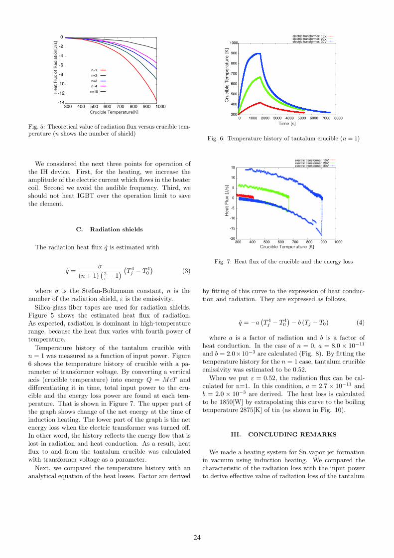
Silica-glass fiber tapes are used for radiation shields.Figure 5 shows the estimated heat flux of radiation.As expected, radiation is dominant in high-temperaturerange, because the heat flux varies with fourth power oftemperature.
Temperature history of the tantalum crucible withn = 1 was measured as a function of input power. Figure6 shows the temperature history of crucible with a pa-rameter of transformer voltage. By converting a verticalaxis (crucible temperature) into energy Q = McT anddifferentiating it in time, total input power to the cru-cible and the energy loss power are found at each tem-perature. That is shown in Figure 7. The upper part ofthe graph shows change of the net energy at the time ofinduction heating. The lower part of the graph is the netenergy loss when the electric transformer was turned off.In other word, the history reflects the energy flow that islost in radiation and heat conduction. As a result, heatflux to and from the tantalum crucible was calculatedwith transformer voltage as a parameter.
Next, we compared the temperature history with ananalytical equation of the heat losses. Factor are derived
300
400
500
600
700
800
900
1000
0 1000 2000 3000 4000 5000 6000 7000 8000
Crucible Temperature [K]
Time [s]
electric transformer: 10Velectric transformer: 20Velectric transformer: 30V
Fig. 6: Temperature history of tantalum crucible (n = 1)
-20
-15
-10
-5
0
5
10
15
300 400 500 600 700 800 900 1000
Heat Flux [J/s]
Crucible Temperature [K]
electric transformer: 10Velectric transformer: 20Velectric transformer: 30V
Fig. 7: Heat flux of the crucible and the energy loss
by fitting of this curve to the expression of heat conduc-tion and radiation. They are expressed as follows,
q = −a(T 4
j − T 40
)− b (Tj − T0) (4)
where a is a factor of radiation and b is a factor ofheat conduction. In the case of n = 0, a = 8.0 × 10⁻¹¹
and b = 2.0×10⁻³ are calculated (Fig. 8). By fitting thetemperature history for the n = 1 case, tantalum crucibleemissivity was estimated to be 0.52.
When we put ε = 0.52, the radiation flux can be cal-culated for n=1. In this condition, a = 2.7 × 10⁻¹¹ andb = 2.0 × 10⁻³ are derived. The heat loss is calculatedto be 1850[W] by extrapolating this curve to the boilingtemperature 2875[K] of tin (as shown in Fig. 10).
III. CONCLUDING REMARKS
We made a heating system for Sn vapor jet formationin vacuum using induction heating. We compared thecharacteristic of the radiation loss with the input powerto derive effective value of radiation loss of the tantalum
2424
-60
-50
-40
-30
-20
-10
0
10
20
300 400 500 600 700 800 900 1000
n=1n=0
-a*(x**4-300**4)-b*(x-300)
-a(T -T )-b(T -T )4 4j j 00
Heat Flux [J/s]
Crucible Temperature [K]
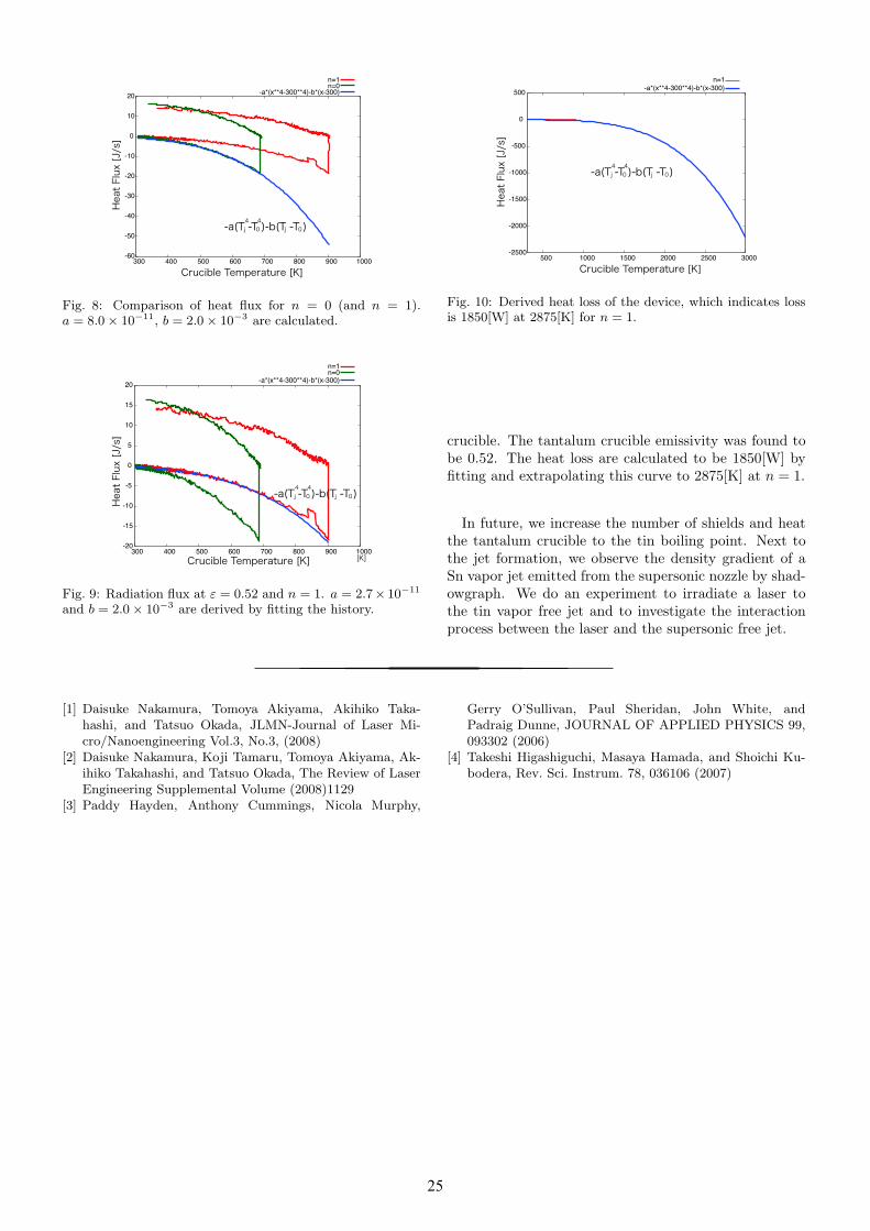
Fig. 8: Comparison of heat flux for n = 0 (and n = 1).a = 8.0 × 10⁻¹¹, b = 2.0 × 10⁻³ are calculated.
-20
-15
-10
-5
0
5
10
15
20
300 400 500 600 700 800 900 1000
-a(T -T )-b(T -T )4 4j j 00
[K]
Heat Flux [J/s]
Crucible Temperature [K]
n=1n=0
-a*(x**4-300**4)-b*(x-300)
Fig. 9: Radiation flux at ε = 0.52 and n = 1. a = 2.7× 10⁻¹¹
and b = 2.0 × 10⁻³ are derived by fitting the history.
-2500
-2000
-1500
-1000
-500
0
500
500 1000 1500 2000 2500 3000
n=1
-a*(x**4-300**4)-b*(x-300)
-a(T -T )-b(T -T )4 4j j 00
Heat Flux [J/s]
Crucible Temperature [K]
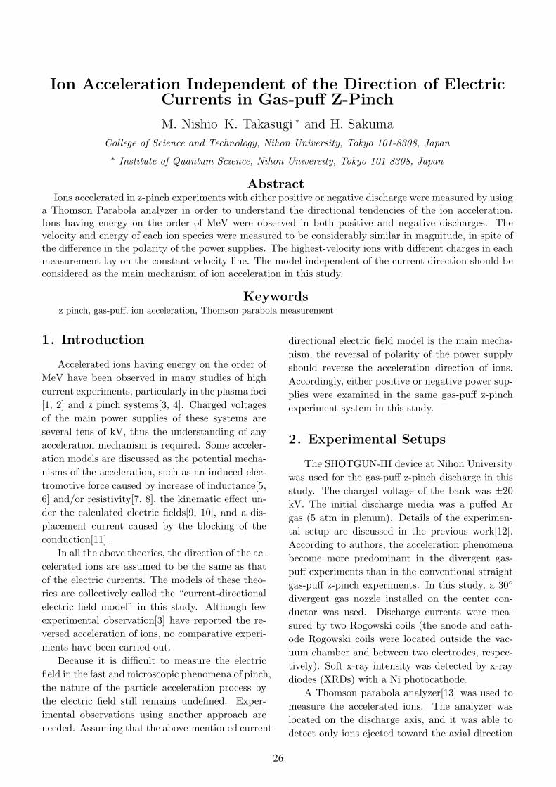
Fig. 10: Derived heat loss of the device, which indicates lossis 1850[W] at 2875[K] for n = 1.
crucible. The tantalum crucible emissivity was found tobe 0.52. The heat loss are calculated to be 1850[W] byfitting and extrapolating this curve to 2875[K] at n = 1.
In future, we increase the number of shields and heatthe tantalum crucible to the tin boiling point. Next tothe jet formation, we observe the density gradient of aSn vapor jet emitted from the supersonic nozzle by shad-owgraph. We do an experiment to irradiate a laser tothe tin vapor free jet and to investigate the interactionprocess between the laser and the supersonic free jet.
[1] Daisuke Nakamura, Tomoya Akiyama, Akihiko Taka-hashi, and Tatsuo Okada, JLMN-Journal of Laser Mi-cro/Nanoengineering Vol.3, No.3, (2008)
[2] Daisuke Nakamura, Koji Tamaru, Tomoya Akiyama, Ak-ihiko Takahashi, and Tatsuo Okada, The Review of LaserEngineering Supplemental Volume (2008)1129
[3] Paddy Hayden, Anthony Cummings, Nicola Murphy,
Gerry O’Sullivan, Paul Sheridan, John White, andPadraig Dunne, JOURNAL OF APPLIED PHYSICS 99,093302 (2006)
[4] Takeshi Higashiguchi, Masaya Hamada, and Shoichi Ku-bodera, Rev. Sci. Instrum. 78, 036106 (2007)
2525
Ion Acceleration Independent of the Direction of ElectricCurrents in Gas-puff Z-Pinch
M. Nishio K. Takasugi ∗ and H. Sakuma
College of Science and Technology, Nihon University, Tokyo 101-8308, Japan∗ Institute of Quantum Science, Nihon University, Tokyo 101-8308, Japan
AbstractIons accelerated in z-pinch experiments with either positive or negative discharge were measured by using
a Thomson Parabola analyzer in order to understand the directional tendencies of the ion acceleration.Ions having energy on the order of MeV were observed in both positive and negative discharges. Thevelocity and energy of each ion species were measured to be considerably similar in magnitude, in spite ofthe difference in the polarity of the power supplies. The highest-velocity ions with different charges in eachmeasurement lay on the constant velocity line. The model independent of the current direction should beconsidered as the main mechanism of ion acceleration in this study.
Keywordsz pinch, gas-puff, ion acceleration, Thomson parabola measurement
1. Introduction
Accelerated ions having energy on the order ofMeV have been observed in many studies of highcurrent experiments, particularly in the plasma foci[1, 2] and z pinch systems[3, 4]. Charged voltagesof the main power supplies of these systems areseveral tens of kV, thus the understanding of anyacceleration mechanism is required. Some acceler-ation models are discussed as the potential mecha-nisms of the acceleration, such as an induced elec-tromotive force caused by increase of inductance[5,6] and/or resistivity[7, 8], the kinematic effect un-der the calculated electric fields[9, 10], and a dis-placement current caused by the blocking of theconduction[11].
In all the above theories, the direction of the ac-celerated ions are assumed to be the same as thatof the electric currents. The models of these theo-ries are collectively called the “current-directionalelectric field model” in this study. Although fewexperimental observation[3] have reported the re-versed acceleration of ions, no comparative experi-ments have been carried out.
Because it is difficult to measure the electricfield in the fast and microscopic phenomena of pinch,the nature of the particle acceleration process bythe electric field still remains undefined. Exper-imental observations using another approach areneeded. Assuming that the above-mentioned current-
directional electric field model is the main mecha-nism, the reversal of polarity of the power supplyshould reverse the acceleration direction of ions.Accordingly, either positive or negative power sup-plies were examined in the same gas-puff z-pinchexperiment system in this study.
2. Experimental Setups
The SHOTGUN-III device at Nihon Universitywas used for the gas-puff z-pinch discharge in thisstudy. The charged voltage of the bank was ±20kV. The initial discharge media was a puffed Argas (5 atm in plenum). Details of the experimen-tal setup are discussed in the previous work[12].According to authors, the acceleration phenomenabecome more predominant in the divergent gas-puff experiments than in the conventional straightgas-puff z-pinch experiments. In this study, a 30◦
divergent gas nozzle installed on the center con-ductor was used. Discharge currents were mea-sured by two Rogowski coils (the anode and cath-ode Rogowski coils were located outside the vac-uum chamber and between two electrodes, respec-tively). Soft x-ray intensity was detected by x-raydiodes (XRDs) with a Ni photocathode.
A Thomson parabola analyzer[13] was used tomeasure the accelerated ions. The analyzer waslocated on the discharge axis, and it was able todetect only ions ejected toward the axial direction
2626
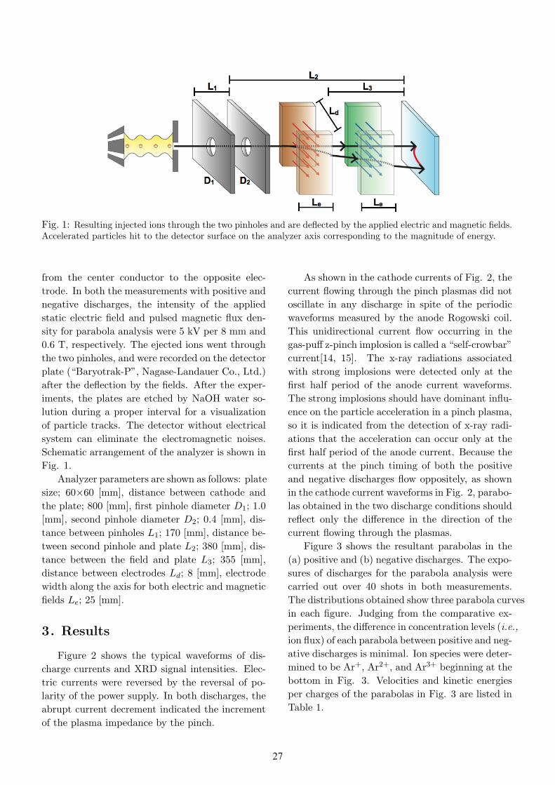
Fig. 1: Resulting injected ions through the two pinholes and are deflected by the applied electric and magnetic fields.Accelerated particles hit to the detector surface on the analyzer axis corresponding to the magnitude of energy.
from the center conductor to the opposite elec-trode. In both the measurements with positive andnegative discharges, the intensity of the appliedstatic electric field and pulsed magnetic flux den-sity for parabola analysis were 5 kV per 8 mm and0.6 T, respectively. The ejected ions went throughthe two pinholes, and were recorded on the detectorplate (“Baryotrak-P”, Nagase-Landauer Co., Ltd.)after the deflection by the fields. After the exper-iments, the plates are etched by NaOH water so-lution during a proper interval for a visualizationof particle tracks. The detector without electricalsystem can eliminate the electromagnetic noises.Schematic arrangement of the analyzer is shown inFig. 1.
Analyzer parameters are shown as follows: platesize; 60×60 [mm], distance between cathode andthe plate; 800 [mm], first pinhole diameter D1; 1.0[mm], second pinhole diameter D2; 0.4 [mm], dis-tance between pinholes L1; 170 [mm], distance be-tween second pinhole and plate L2; 380 [mm], dis-tance between the field and plate L3; 355 [mm],distance between electrodes Ld; 8 [mm], electrodewidth along the axis for both electric and magneticfields Le; 25 [mm].
3. Results
Figure 2 shows the typical waveforms of dis-charge currents and XRD signal intensities. Elec-tric currents were reversed by the reversal of po-larity of the power supply. In both discharges, theabrupt current decrement indicated the incrementof the plasma impedance by the pinch.
As shown in the cathode currents of Fig. 2, thecurrent flowing through the pinch plasmas did notoscillate in any discharge in spite of the periodicwaveforms measured by the anode Rogowski coil.This unidirectional current flow occurring in thegas-puff z-pinch implosion is called a “self-crowbar”current[14, 15]. The x-ray radiations associatedwith strong implosions were detected only at thefirst half period of the anode current waveforms.The strong implosions should have dominant influ-ence on the particle acceleration in a pinch plasma,so it is indicated from the detection of x-ray radi-ations that the acceleration can occur only at thefirst half period of the anode current. Because thecurrents at the pinch timing of both the positiveand negative discharges flow oppositely, as shownin the cathode current waveforms in Fig. 2, parabo-las obtained in the two discharge conditions shouldreflect only the difference in the direction of thecurrent flowing through the plasmas.
Figure 3 shows the resultant parabolas in the(a) positive and (b) negative discharges. The expo-sures of discharges for the parabola analysis werecarried out over 40 shots in both measurements.The distributions obtained show three parabola curvesin each figure. Judging from the comparative ex-periments, the difference in concentration levels (i.e.,ion flux) of each parabola between positive and neg-ative discharges is minimal. Ion species were deter-mined to be Ar+, Ar2+, and Ar3+ beginning at thebottom in Fig. 3. Velocities and kinetic energiesper charges of the parabolas in Fig. 3 are listed inTable 1.
2727
a
b
Fig. 2: Typical waveforms of discharge currentsand XRD signal intensities with (a) positive and(b) negative discharges.
4. Discussions
Comparing experiments of positive and nega-tive discharges, three results were obtained: (1)Ions having energy on the order of MeV were ob-served in measurements of both positive and nega-tive discharges. (2) The velocity and energy of eachion species were measured to have similar magni-tudes of accelerations both in the same and oppo-site direction of the electric currents, as shown inTable 1. (3) The highest velocity ions with dif-ferent charges in each figure lay on the constant-velocity lines (eq. 6 in ref.[13]). These results showthat the direction of the acceleration could not de-pend on the direction of currents. This contradictsthe existing current-directional electric field model,because ions should not be accelerated toward theopposite direction to the supposed strong electricfields dependent on the current direction.
The reasonable mechanisms of particle acceler-ation from the z-pinch plasma in this study are con-cluded to have no dependence of the electric currentdirection. The models of the current independentmodel listed previously are evaluated as follows.
Fig. 3: Resultant parabola curves in measurementswith (a) positive and (b) negative discharges.
(1) Thermal energization with the fluid dynamicalinstabilities of sausage instability[16] and/or kinkinstability[17]. However it cannot explain sharpboundary of upper velocity limit. (2) Trappingeffect by the axially propagating potential troughgenerated in the two-stream instability [18] It canexplain sharp boundary of upper velocity limit asthe phase velocity of propagating potential, how-ever may not explain the gradual boundary of lowervelocity regime. (3) Mechanical reflection by theimploding current sheet[19] It can explain sharpboundary of upper velocity limit and also can ex-plain current-directional independency, in addition,may explain the anisotropy of axial ion distribu-tion.
The third model, that is mechanical reflectionmodel proposed by Gureev (1980), is considered tobe the most reasonable model. In short time ofpinch phenomena, the strong acceleration of par-ticles may needs multiple head-on collisions withimploding wall like first-order shockwave Fermi ac-
2828
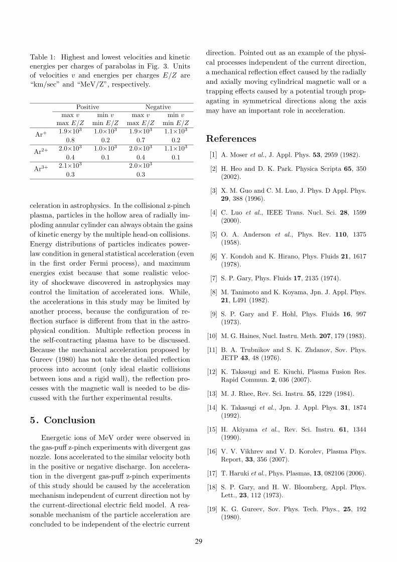
Table 1: Highest and lowest velocities and kineticenergies per charges of parabolas in Fig. 3. Unitsof velocities v and energies per charges E/Z are“km/sec” and “MeV/Z”, respectively.
Positive Negativemax v min v max v min v
max E/Z min E/Z max E/Z min E/Z
Ar+ 1.9×10³ 1.0×10³ 1.9×10³ 1.1×10³
0.8 0.2 0.7 0.2
Ar2+ 2.0×10³ 1.0×10³ 2.0×10³ 1.1×10³
0.4 0.1 0.4 0.1
Ar3+ 2.1×10³ 2.0×10³
0.3 0.3
celeration in astrophysics. In the collisional z-pinchplasma, particles in the hollow area of radially im-ploding annular cylinder can always obtain the gainsof kinetic energy by the multiple head-on collisions.Energy distributions of particles indicates power-law condition in general statistical acceleration (evenin the first order Fermi process), and maximumenergies exist because that some realistic veloc-ity of shockwave discovered in astrophysics maycontrol the limitation of accelerated ions. While,the accelerations in this study may be limited byanother process, because the configuration of re-flection surface is different from that in the astro-physical condition. Multiple reflection process inthe self-contracting plasma have to be discussed.Because the mechanical acceleration proposed byGureev (1980) has not take the detailed reflectionprocess into account (only ideal elastic collisionsbetween ions and a rigid wall), the reflection pro-cesses with the magnetic wall is needed to be dis-cussed with the further experimental results.
5. Conclusion
Energetic ions of MeV order were observed inthe gas-puff z-pinch experiments with divergent gasnozzle. Ions accelerated to the similar velocity bothin the positive or negative discharge. Ion accelera-tion in the divergent gas-puff z-pinch experimentsof this study should be caused by the accelerationmechanism independent of current direction not bythe current-directional electric field model. A rea-sonable mechanism of the particle acceleration areconcluded to be independent of the electric current
direction. Pointed out as an example of the physi-cal processes independent of the current direction,a mechanical reflection effect caused by the radiallyand axially moving cylindrical magnetic wall or atrapping effects caused by a potential trough prop-agating in symmetrical directions along the axismay have an important role in acceleration.
References
[1] A. Moser et al., J. Appl. Phys. 53, 2959 (1982).
[2] H. Heo and D. K. Park. Physica Scripta 65, 350(2002).
[3] X. M. Guo and C. M. Luo, J. Phys. D Appl. Phys.29, 388 (1996).
[4] C. Luo et al., IEEE Trans. Nucl. Sci. 28, 1599(2000).
[5] O. A. Anderson et al., Phys. Rev. 110, 1375(1958).
[6] Y. Kondoh and K. Hirano, Phys. Fluids 21, 1617(1978).
[7] S. P. Gary, Phys. Fluids 17, 2135 (1974).
[8] M. Tanimoto and K. Koyama, Jpn. J. Appl. Phys.21, L491 (1982).
[9] S. P. Gary and F. Hohl, Phys. Fluids 16, 997(1973).
[10] M. G. Haines, Nucl. Instru. Meth. 207, 179 (1983).
[11] B. A. Trubnikov and S. K. Zhdanov, Sov. Phys.JETP 43, 48 (1976).
[12] K. Takasugi and E. Kiuchi, Plasma Fusion Res.Rapid Commun. 2, 036 (2007).
[13] M. J. Rhee, Rev. Sci. Instru. 55, 1229 (1984).
[14] K. Takasugi et al., Jpn. J. Appl. Phys. 31, 1874(1992).
[15] H. Akiyama et al., Rev. Sci. Instru. 61, 1344(1990).
[16] V. V. Vikhrev and V. D. Korolev, Plasma Phys.Report, 33, 356 (2007).
[17] T. Haruki et al., Phys. Plasmas, 13, 082106 (2006).
[18] S. P. Gary, and H. W. Bloomberg, Appl. Phys.Lett., 23, 112 (1973).
[19] K. G. Gureev, Sov. Phys. Tech. Phys., 25, 192(1980).
2929
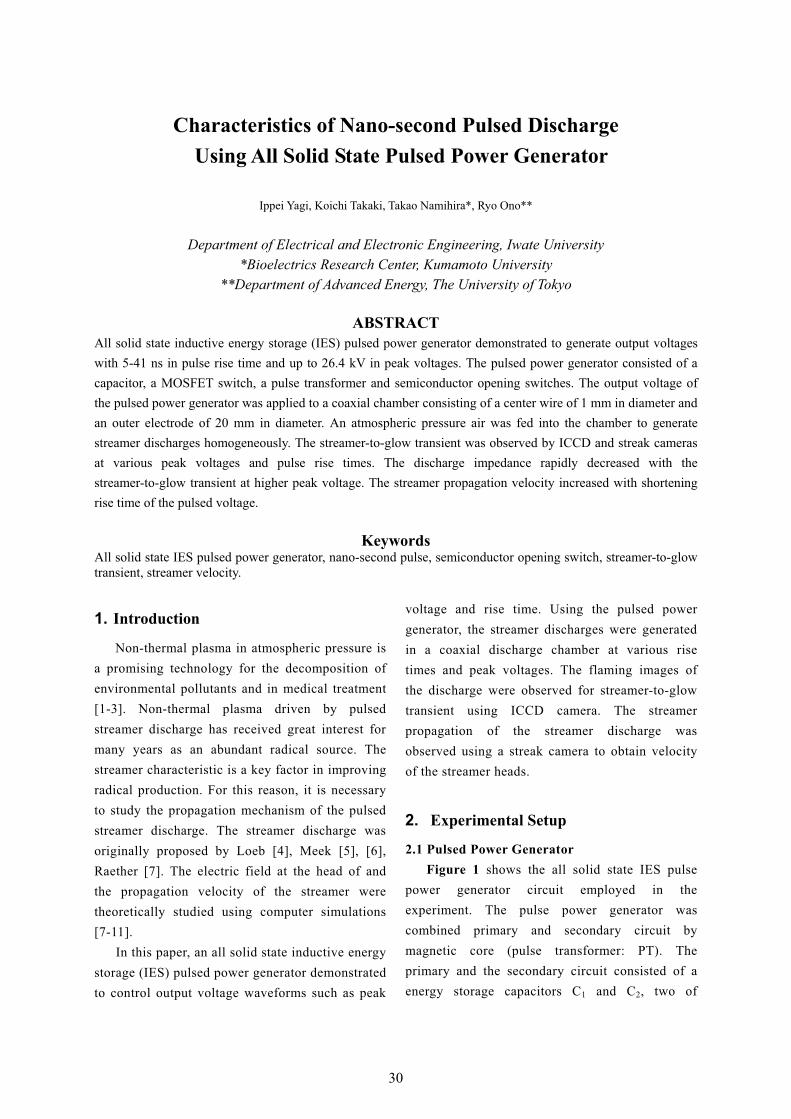
� �
Characteristics of Nano-second Pulsed Discharge Using All Solid State Pulsed Power Generator
Ippei Yagi, Koichi Takaki, Takao Namihira*, Ryo Ono**
Department of Electrical and Electronic Engineering, Iwate University *Bioelectrics Research Center, Kumamoto University
**Department of Advanced Energy, The University of Tokyo
ABSTRACT All solid state inductive energy storage (IES) pulsed power generator demonstrated to generate output voltages with 5-41 ns in pulse rise time and up to 26.4 kV in peak voltages. The pulsed power generator consisted of a capacitor, a MOSFET switch, a pulse transformer and semiconductor opening switches. The output voltage of the pulsed power generator was applied to a coaxial chamber consisting of a center wire of 1 mm in diameter and an outer electrode of 20 mm in diameter. An atmospheric pressure air was fed into the chamber to generate streamer discharges homogeneously. The streamer-to-glow transient was observed by ICCD and streak cameras at various peak voltages and pulse rise times. The discharge impedance rapidly decreased with the streamer-to-glow transient at higher peak voltage. The streamer propagation velocity increased with shortening rise time of the pulsed voltage.
Keywords
All solid state IES pulsed power generator, nano-second pulse, semiconductor opening switch, streamer-to-glow transient, streamer velocity.
1. Introduction
Non-thermal plasma in atmospheric pressure is a promising technology for the decomposition of environmental pollutants and in medical treatment [1-3]. Non-thermal plasma driven by pulsed streamer discharge has received great interest for many years as an abundant radical source. The streamer characteristic is a key factor in improving radical production. For this reason, it is necessary to study the propagation mechanism of the pulsed streamer discharge. The streamer discharge was originally proposed by Loeb [4], Meek [5], [6], Raether [7]. The electric field at the head of and the propagation velocity of the streamer were theoretically studied using computer simulations [7-11].
In this paper, an all solid state inductive energy storage (IES) pulsed power generator demonstrated to control output voltage waveforms such as peak
voltage and rise time. Using the pulsed power generator, the streamer discharges were generated in a coaxial discharge chamber at various rise times and peak voltages. The flaming images of the discharge were observed for streamer-to-glow transient using ICCD camera. The streamer propagation of the streamer discharge was observed using a streak camera to obtain velocity of the streamer heads.
2. Experimental Setup
2.1 Pulsed Power Generator Figure 1 shows the all solid state IES pulse
power generator circuit employed in the experiment. The pulse power generator was combined primary and secondary circuit by magnetic core (pulse transformer: PT). The primary and the secondary circuit consisted of a energy storage capacitors C1 and C2, two of
3030
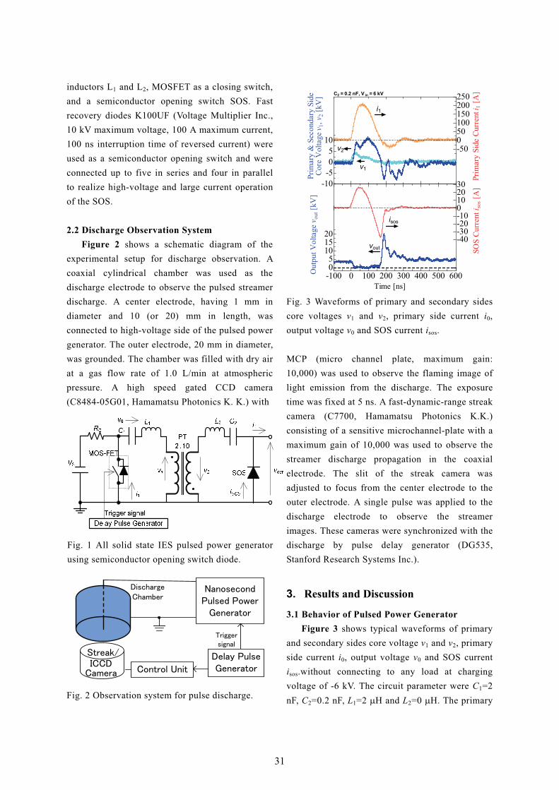
inductors L1 and L2, MOSFET as a closing switch, and a semiconductor opening switch SOS. Fast recovery diodes K100UF (Voltage Multiplier Inc., 10 kV maximum voltage, 100 A maximum current, 100 ns interruption time of reversed current) were used as a semiconductor opening switch and were connected up to five in series and four in parallel to realize high-voltage and large current operation of the SOS.
2.2 Discharge Observation System
Figure 2 shows a schematic diagram of the experimental setup for discharge observation. A coaxial cylindrical chamber was used as the discharge electrode to observe the pulsed streamer discharge. A center electrode, having 1 mm in diameter and 10 (or 20) mm in length, was connected to high-voltage side of the pulsed power generator. The outer electrode, 20 mm in diameter, was grounded. The chamber was filled with dry air at a gas flow rate of 1.0 L/min at atmospheric pressure. A high speed gated CCD camera (C8484-05G01, Hamamatsu Photonics K. K.) with
Fig. 1 All solid state IES pulsed power generator using semiconductor opening switch diode.
)���$ ���0�.�$ 0�.�1 ��2 � ����
��� ��
3 �%�.�$ �2 � ����
����� �$����
3�$�(��� ��(��/ �
4� ��5#��3
������6��
Fig. 2 Observation system for pulse discharge.
-10-505
10-50050100150200250
Prim
ary
& S
econ
dary
Sid
eC
ore
Vol
tage
v 1, v
2 [kV
]
Prim
ary
Side
Cur
rent
i 1 [A
]
v2
-100 0 100 200 300 400 500 60005
101520 -40
-30-20-100102030
Time [ns]
Out
put V
olta
ge v o
ut [k
V]
C2 = 0.2 nF, V in = 6 kV
SOS
Curr
ent i
sos [
A]
i1
v1
vout
isos
Fig. 3 Waveforms of primary and secondary sides core voltages v1 and v2, primary side current i0, output voltage v0 and SOS current isos. MCP (micro channel plate, maximum gain: 10,000) was used to observe the flaming image of light emission from the discharge. The exposure time was fixed at 5 ns. A fast-dynamic-range streak camera (C7700, Hamamatsu Photonics K.K.) consisting of a sensitive microchannel-plate with a maximum gain of 10,000 was used to observe the streamer discharge propagation in the coaxial electrode. The slit of the streak camera was adjusted to focus from the center electrode to the outer electrode. A single pulse was applied to the discharge electrode to observe the streamer images. These cameras were synchronized with the discharge by pulse delay generator (DG535, Stanford Research Systems Inc.).
3. Results and Discussion
3.1 Behavior of Pulsed Power Generator Figure 3 shows typical waveforms of primary
and secondary sides core voltage v1 and v2, primary side current i0, output voltage v0 and SOS current isos.without connecting to any load at charging voltage of -6 kV. The circuit parameter were C1=2 nF, C2=0.2 nF, L1=2 �H and L2=0 �H. The primary
3131
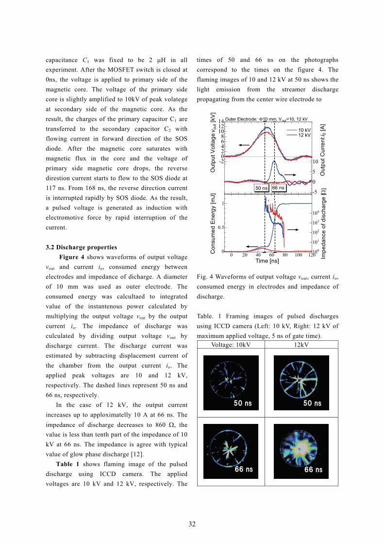
capacitance C1 was fixed to be 2 �H in all experiment. After the MOSFET switch is closed at 0ns, the voltage is applied to primary side of the magnetic core. The voltage of the primary side core is slightly amplified to 10kV of peak volatege at secondary side of the magnetic core. As the result, the charges of the primary capacitor C1 are transferred to the secondary capacitor C2 with flowing current in forward direction of the SOS diode. After the magnetic core saturates with magnetic flux in the core and the voltage of primary side magnetic core drops, the reverse direstion current starts to flow to the SOS diode at 117 ns. From 168 ns, the reverse direction current is interrupted rapidly by SOS diode. As the result, a pulsed voltage is generated as induction with electromotive force by rapid interruption of the current.
3.2 Discharge properties
Figure 4 shows waveforms of output voltage vout and current io, consumed energy between electrodes and impedance of dicharge. A diameter of 10 mm was used as outer electrode. The consumed energy was calcultaed to integrated value of the instantenous power calculated by multiplying the output voltage vout by the output current io. The impedance of discharge was culculated by dividing output voltage vout by discharge current. The discharge current was estimated by subtracting displacement current of the chamber from the output current io. The applied peak voltages are 10 and 12 kV, respectively. The dashed lines represent 50 ns and 66 ns, respectively.
In the case of 12 kV, the output current increases up to apploximatelly 10 A at 66 ns. The impedance of discharge decreases to 860 �� the value is less than tenth part of the impedance of 10 kV at 66 ns. The impedance is agree with typical value of glow phase discharge [12].
Table 1 shows flaming image of the pulsed discharge using ICCD camera. The applied voltages are 10 kV and 12 kV, respectively. The
times of 50 and 66 ns on the photographs correspond to the times on the figure 4. The flaming images of 10 and 12 kV at 50 ns shows the light emission from the streamer discharge propagating from the center wire electrode to
Fig. 4 Waveforms of output voltage vout, current io, consumed energy in electrodes and impedance of discharge. Table. 1 Framing images of pulsed discharges using ICCD camera (Left: 10 kV, Right: 12 kV of maximum applied voltage, 5 ns of gate time).
Voltage: 10kV 12kV
-202468
101214
-5
0
5
10
Out
put V
olta
ge v o
ut [k
V]
Out
put C
urre
nt i 0
[A]
Time [ns]
Outer Electrode: �10 mm, Vout=10, 12 kV
10 kV 12 kV
0 20 40 60 80 100 1200
0.5
1
100
101
102
103
104C
onsu
med
Ene
rgy
[mJ]
Impe
danc
e of
dis
char
ge [�
50 ns 66 ns
������
������ ������
������
3232
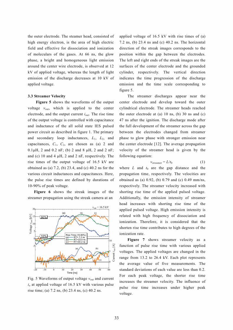
the outer electrode. The steamer head, consisted of high energy electron, is the area of high electric field and effective for dissociation and ionization of moleculars of the gases. At 66 ns, the glow phase, a bright and homogeneous light emission around the center wire electrode, is observed at 12 kV of applied voltage, whereas the length of light emission of the discharge decreases at 10 kV of applied voltage.
3.3 Streamer Velocity
Figure 5 shows the waveforms of the output voltage vout, which is applied to the center electrode, and the output current iout. The rise time of the output voltage is controlled with capacitance and inductance of the all solid state IES pulsed power circuit as described in figure 1. The primary and secondary loop inductances, L1, L2, and capacitances, C1, C2, are chosen as (a) 2 and 0.1�H, 2 and 0.2 nF; (b) 2 and 8 �H, 2 and 2 nF; and (c) 10 and 4 �H, 2 and 2 nF, respectively. The rise times of the output voltage of 16.5 kV are obtained as (a) 7.2, (b) 23.4, and (c) 40.2 ns for the various circuit inductances and capacitances. Here, the pulse rise times are defined by durations of 10-90% of peak voltage.
Figure 6 shows the streak images of the streamer propagation using the streak camera at an
-20 -10 0 10 20 30 40 50 60
-5
0
5
10
15
20
0
5
10
Time [ns]
Vol
tage
vou
t [kV
]
Cur
rent
i out
[A]
Rise Time (10-90%)(a) RT= 7.2 ns(b) RT=23.4 ns (c) RT=40.2 ns
vout = 16.5 kV
90%
10%
(a)
(b)
(b) (c)
(c)
(a)
Fig. 5 Waveforms of output voltage vout and current io at applied voltage of 16.5 kV with various pulse rise time; (a) 7.2 ns, (b) 23.4 ns, (c) 40.2 ns.
applied voltage of 16.5 kV with rise times of (a) 7.2 ns, (b) 23.4 ns and (c) 40.2 ns. The horizontal direction of the streak images corresponds to the position within the gap between the electrodes. The left and right ends of the streak images are the surfaces of the center electrode and the grounded cylinder, respectively. The vertical direction indicates the time progression of the discharge emission and the time scale corresponding to figure 5.
The streamer discharges appear near the center electrode and develop toward the outer cylindrical electrode. The streamer heads reached the outer electrode at (a) 10 ns, (b) 30 ns and (c) 47 ns after the ignition. The discharge mode after the full development of the streamer across the gap between the electrodes changed from streamer phase to glow phase with stronger emission near the center electrode [12]. The average propagation velocity of the streamer head is given by the following equation:
vstreamer = L/t0 (1) where L and t0 are the gap distance and the propagation time, respectively. The velocities are obtained as (a) 0.92, (b) 0.79 and (c) 0.49 mm/ns, respectively. The streamer velocity increased with shorting rise time of the applied pulsed voltage. Additionally, the emission intensity of streamer head increases with shorting rise time of the applied pulsed voltage. High emission intensity is related with high frequency of dissociation and ionization. Therefore, it is considered that the shorten rise time contributes to high degrees of the ionization rate.
Figure 7 shows streamer velocity as a function of pulse rise time with various applied voltages. The applied voltages are changed in the range from 13.2 to 26.4 kV. Each plot represents the average value of five measurements. The standard deviations of each value are less than 0.2. For each peak voltage, the shorter rise time increases the streamer velocity. The influence of pulse rise time increases under higher peak voltage.
3333
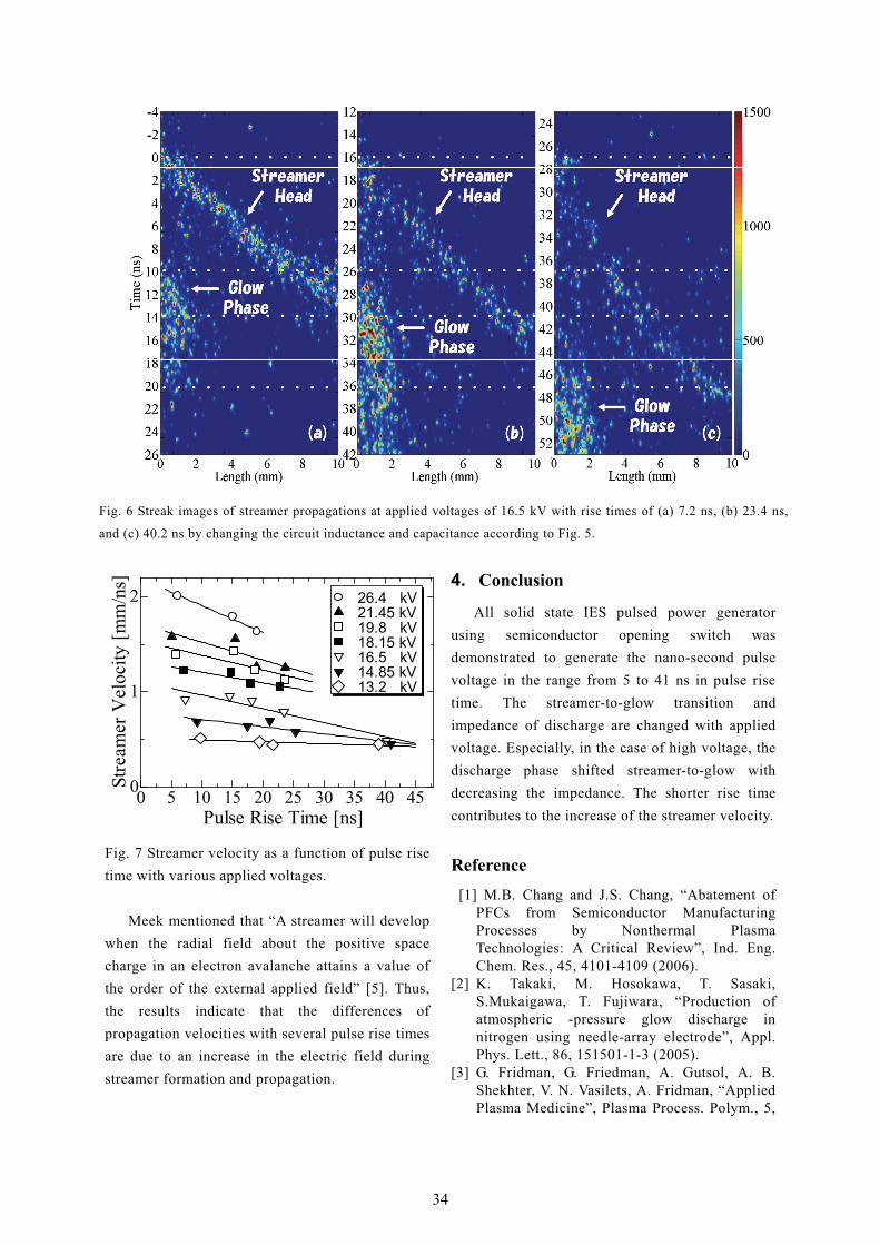
0 5 10 15 20 25 30 35 40 450
1
2
Pulse Rise Time [ns]
Stre
amer
Vel
ocity
[mm
/ns]
26.4 kV 21.45 kV 19.8 kV 18.15 kV 16.5 kV 14.85 kV 13.2 kV
Fig. 7 Streamer velocity as a function of pulse rise time with various applied voltages.
Meek mentioned that “A streamer will develop when the radial field about the positive space charge in an electron avalanche attains a value of the order of the external applied field” [5]. Thus, the results indicate that the differences of propagation velocities with several pulse rise times are due to an increase in the electric field during streamer formation and propagation.
4. Conclusion
All solid state IES pulsed power generator using semiconductor opening switch was demonstrated to generate the nano-second pulse voltage in the range from 5 to 41 ns in pulse rise time. The streamer-to-glow transition and impedance of discharge are changed with applied voltage. Especially, in the case of high voltage, the discharge phase shifted streamer-to-glow with decreasing the impedance. The shorter rise time contributes to the increase of the streamer velocity.
Reference [1] M.B. Chang and J.S. Chang, “Abatement of
PFCs from Semiconductor Manufacturing Processes by Nonthermal Plasma Technologies: A Critical Review”, Ind. Eng. Chem. Res., 45, 4101-4109 (2006).
[2] K. Takaki, M. Hosokawa, T. Sasaki, S.Mukaigawa, T. Fujiwara, “Production of atmospheric -pressure glow discharge in nitrogen using needle-array electrode”, Appl. Phys. Lett., 86, 151501-1-3 (2005).
[3] G. Fridman, G. Friedman, A. Gutsol, A. B. Shekhter, V. N. Vasilets, A. Fridman, “Applied Plasma Medicine”, Plasma Process. Polym., 5,
Fig. 6 Streak images of streamer propagations at applied voltages of 16.5 kV with rise times of (a) 7.2 ns, (b) 23.4 ns,
and (c) 40.2 ns by changing the circuit inductance and capacitance according to Fig. 5.
3434
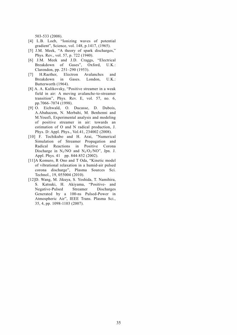
503-533 (2008). [4] L.B. Loeb, “Ionizing waves of potential
gradient”, Science, vol. 148, p.1417, (1965). [5] J.M. Meek, “A theory of spark discharges,”
Phys. Rev., vol. 57, p. 722 (1940). [6] J.M. Meek and J.D. Craggs, “Electrical
Breakdown of Gases”, Oxford, U.K.: Clarendon, pp. 251–290 (1953).
[7] H.Raether, Electron Avalanches and Breakdown in Gases. London, U.K.: Butterworth (1964).
[8] A. A. Kulikovsky, “Positive streamer in a weak field in air: A moving avalanche-to-streamer transition”, Phys. Rev. E, vol. 57, no. 6, pp.7066–7074 (1998).
[9] O. Eichwald, O. Ducasse, D. Dubois, A.Abahazem, N. Merbahi, M. Benhenni and M.Yousfi, Experimental analysis and modeling of positive streamer in air: towards an estimation of O and N radical production, J. Phys. D: Appl. Phys., Vol.41, 234002 (2008).
[10] F. Tochikubo and H. Arai, ”Numerical Simulation of Streamer Propagation and Radical Reactions in Positive Corona Discharge in N2/NO and N2/O2/NO”, Jpn. J. Appl. Phys. 41 pp. 844-852 (2002).
[11]A Komuro, R Ono and T Oda, “Kinetic model of vibrational relaxation in a humid-air pulsed corona discharge”, Plasma Sources Sci. Technol., 19, 055004 (2010).
[12]D. Wang, M. Jikuya, S. Yoshida, T. Namihira, S. Katsuki, H. Akiyama, “Positive- and Negative-Pulsed Streamer Discharges Generated by a 100-ns Pulsed-Power in Atmospheric Air”, IEEE Trans. Plasma Sci., 35, 4, pp. 1098-1103 (2007).
3535
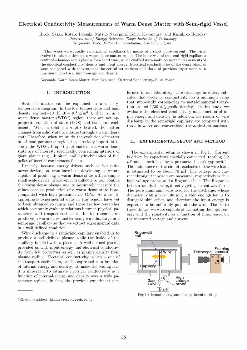
Electrical Conductivity Measurements of Warm Dense Matter with Semi-rigid Vessel
Hiroki Sakai, Kotaro Iwasaki, Mitsuo Nakajima, Tohru Kawamura, and Kazuhiko Horioka∗Department of Energy Sciences, Tokyo Institute of Technology,
Nagatsuta 4259, Midori-ku, Yokohama, 226-8502, Japan
Thin wires were rapidly vaporized in capillaries by means of a short pulse current. The wiresevolved to plasma through a warm dense matter region. The inner wall of the semi-rigid capillariesconfined a homogeneous plasma for a short time, which enabled us to make accurate measurements ofthe electrical conductivity, density and input energy. Electrical conductivities of the dense plasmaswere compared with conventional theoretical estimations and those of previous experiment as afunction of electrical input energy and density.
Keywords: Warm Dense Matter, Wire Explosion, Electrical Conductivity, Pulse-Power
I. INTRODUCTION
State of matter can be explained in a density-temperature diagram. In the low temperature and highdensity regime(−105 K, 10− 104 g/m3 ), that is, in awarm dense matter (WDM) region, there are not ap-propriate equation of state (EOS) and transport coef-ficient. When a solid is abruptly heated, the matterchanges from solid state to plasma through a warm densestate.Therefore, when we study the evolution of matterin a broad parameter region, it is crucially important tostudy the WDM. Properties of matter in a warm densestate are of interest, specifically, concerning interiors ofgiant planet (e.g., Jupiter) and hydrodynamics of fuelpellet of inertial confinement fusion.
Recently, because energy drivers such as fast pulsepower device, ion beam have been developing, so we arecapable of producing a warm dense state with a simplesmall scale device. However, it is difficult to well confinethe warm dense plasma and to accurately measure thevalues because production of a warm dense state is ac-companied with high pressure over GPa. As a result,appropriate experimental data in this region have yetto been obtained so much, and there are few researcheswhich accurately evaluate relations between physical pa-rameters and trasport coefficient. In this research, weproduced a warm dense matter using wire discharge in asemi-rigid capillary so that we extract experimental datain a wall defined condition.
Wire discharge in a semi-rigid capillary enabled us toproduce a well-defined plasma while the inside of thecapillary is filled with a plasma. A well-defined plasmaprovided us with input energy and electrical conductiv-ity from I-V properties as well as plasma density fromplasma radius. Electrical conductivity, which is one ofthe trasport coefficients, can be expressed as a functionof internal-energy and density. To make the scaling law,it is important to estimate electrical conductivity as afunction of internal-energy and density over a wide pa-rameter region. In fact, the previous experiment per-
∗Electronic address: [email protected]
formed in our laboratory; wire discharge in water, indi-cated that electrical conductivity has a minimum valuethat supposedly corresponds to metal-nonmetal transi-tion around 1/30 ρs(ρs:solid density). In this study, weevaluate the electrical conductivity as a function of in-put energy and density. In addition, the results of wiredischarge in the semi-rigid capillary are compared withthose in water and conventional theoretical estimations.
II. EXPERIMENTAL SETUP AND METHOD
The experimental setup is shown in Fig.1. Currentis driven by capacitors coaxially connected, totaling 3.2μF and is switched by a pressurized spark-gap switch.The inductance of the circuit, exclusive of the wire load,is estimated to be about 70 nH. The voltage and cur-rent through the wire were measured, respectively with ahigh voltage probe, and a Rogowski belt. The Rogowskibelt surrounds the wire, directly giving current waveform.The pure aluminum wire used for the discharge, whosediameter is 50 μm or 100 μm, is thin enough for us todisregard skin effect, and therefore the input energy isexpected to be uniformly put into the wire. Thanks tothese things, we were capable of evaluating the input en-ergy and the resistivity as a function of time, based onthe measured voltage and current.
Wire
Gap swich
READYSINGLECONT.
OPENCLOSE
Framing camera
Rogowski coil
Telescope
High voltage probe
V
Capillary
Fig.1 Schematic diagram of experimental setup
3636
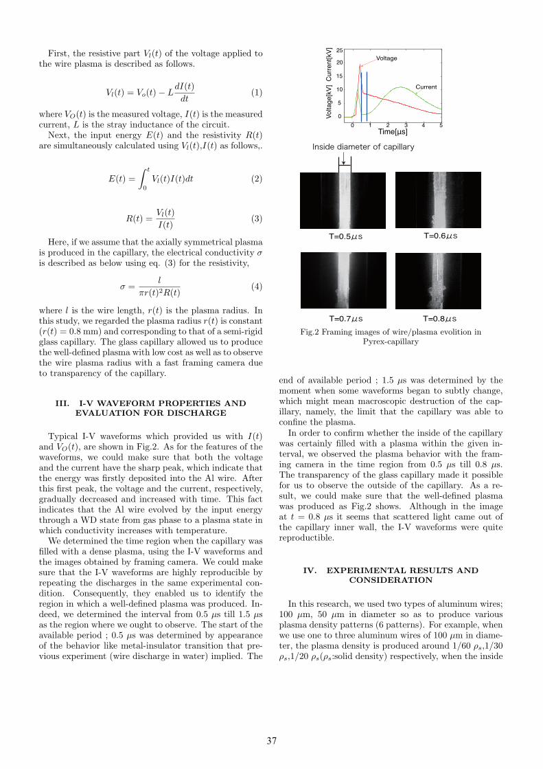
First, the resistive part Vl(t) of the voltage applied tothe wire plasma is described as follows.
Vl(t) = Vo(t)− LdI(t)dt
(1)
where VO(t) is the measured voltage, I(t) is the measuredcurrent, L is the stray inductance of the circuit.
Next, the input energy E(t) and the resistivity R(t)are simultaneously calculated using Vl(t),I(t) as follows,.
E(t) =∫ t
0
Vl(t)I(t)dt (2)
R(t) =Vl(t)I(t)
(3)
Here, if we assume that the axially symmetrical plasmais produced in the capillary, the electrical conductivity σis described as below using eq. (3) for the resistivity,
σ =l
πr(t)2R(t)(4)
where l is the wire length, r(t) is the plasma radius. Inthis study, we regarded the plasma radius r(t) is constant(r(t) = 0.8 mm) and corresponding to that of a semi-rigidglass capillary. The glass capillary allowed us to producethe well-defined plasma with low cost as well as to observethe wire plasma radius with a fast framing camera dueto transparency of the capillary.
III. I-V WAVEFORM PROPERTIES ANDEVALUATION FOR DISCHARGE
Typical I-V waveforms which provided us with I(t)and VO(t), are shown in Fig.2. As for the features of thewaveforms, we could make sure that both the voltageand the current have the sharp peak, which indicate thatthe energy was firstly deposited into the Al wire. Afterthis first peak, the voltage and the current, respectively,gradually decreased and increased with time. This factindicates that the Al wire evolved by the input energythrough a WD state from gas phase to a plasma state inwhich conductivity increases with temperature.
We determined the time region when the capillary wasfilled with a dense plasma, using the I-V waveforms andthe images obtained by framing camera. We could makesure that the I-V waveforms are highly reproducible byrepeating the discharges in the same experimental con-dition. Consequently, they enabled us to identify theregion in which a well-defined plasma was produced. In-deed, we determined the interval from 0.5 μs till 1.5 μsas the region where we ought to observe. The start of theavailable period ; 0.5 μs was determined by appearanceof the behavior like metal-insulator transition that pre-vious experiment (wire discharge in water) implied. The
25
0 1 2 3 4 5Time[μs]
0
5
10
15
20
Vol
tage
[kV
] C
urre
nt[k
V]
Voltage
Current
T=0.5μs
Inside diameter of capillary
T=0.6μs
T=0.7μs T=0.8μsFig.2 Framing images of wire/plasma evolition in
Pyrex-capillary
end of available period ; 1.5 μs was determined by themoment when some waveforms began to subtly change,which might mean macroscopic destruction of the cap-illary, namely, the limit that the capillary was able toconfine the plasma.
In order to confirm whether the inside of the capillarywas certainly filled with a plasma within the given in-terval, we observed the plasma behavior with the fram-ing camera in the time region from 0.5 μs till 0.8 μs.The transparency of the glass capillary made it possiblefor us to observe the outside of the capillary. As a re-sult, we could make sure that the well-defined plasmawas produced as Fig.2 shows. Although in the imageat t = 0.8 μs it seems that scattered light came out ofthe capillary inner wall, the I-V waveforms were quitereproductible.
IV. EXPERIMENTAL RESULTS ANDCONSIDERATION
In this research, we used two types of aluminum wires;100 μm, 50 μm in diameter so as to produce variousplasma density patterns (6 patterns). For example, whenwe use one to three aluminum wires of 100 μm in diame-ter, the plasma density is produced around 1/60 ρs,1/30ρs,1/20 ρs(ρs:solid density) respectively, when the inside
3737
of the capillary was filled with a plasma. Similarly, inthe case of one to three aluminum wires of 50 μm in di-ameter, the produced plasma density are around 1/255ρs,1/125 ρs,1/85 ρs respectively. Typical I-V waveformsfor the respective plasma densities are indicated in Fig.3.We found the time histories depend on the density andcould confirm highly reproductible I-V waveforms. Theirpatterns were qualitatively similar ; a sharp peak in theinitial phase, its collapse, and current evolution. There-fore, we were not only able to obtain the well-definedplasma in the glass capillary within the density regionwhich ranges from 1/255 ρs to 1/20 ρs, but we were ca-pable of getting input energy and electrical conductivitybased on the Eqs.(2) and (4).
The input energy versus conductivity of aluminum wireis shown in Fig.5, which shows change of the conductiv-ity versus the input energy. We determined the availableregion for estimation of conductivity and input energyto be a period while the inside of the capillary was filledwith a plasma. Considering the volume of the capillary,the wire mass and the input energy per unit mass ofthe wire, the relations between plasma states and con-ductivity are uniquely determined. Fig.5 indicates thatconductivity has a minimum at a specific input energypoint for respective plasma densities.
As the conductivity and the input energy per unit massand density of Al plasma were well defined, we could get
0 1 2 3 4 5 6 7
Vol
tage
[kV
] Cur
rent
[kA
]
-5
0
5
10
15
20
25
Voltage
Current
(d) ρ/ρs = 1/85
Volta
ge[k
V]
Curr
ent[kA
]
-5
0
5
10
15
20
25
0 1 2 3 4 5 6 7
(c) ρ/ρs = 1/60
Voltage
Current
70 1 2 3 4 5 6
Voltage
Current
Vol
tage
[kV
] Cur
rent
[kA
]
-5
0
5
10
15
20
25
(b) ρ/ρs = 1/30
Voltage
Current
Vol
tage
[kV
] Cur
rent
[kA
]
-5
0
5
10
15
20
25
0 1 2 3 4 5 6 7
(a) ρ/ρs = 1/20
Voltage
Current
0 1 2 3 4 5 6 7
Vol
tage
[kV
] Cur
rent
[kA
]
-5
0
5
10
15
20
25
(f) ρ/ρs = 1/255
0 1 2 3 4 5 6 7
(e) ρ/ρs = 1/125
Vol
tage
[kV
] Cur
rent
[kA
]
-5
0
5
10
15
20
25
Current
Voltage
Fig.3 Typical waveforms of voltage and current of Al-wiredischarges (Vc = 10 kV, in glass capillary)
1/20
1/30
1/60
1/85
1/125
1/255
160
120
80
40
0
0 1 2 3 4 5 6 7
ρ/ρs=
Input energy[J]
Time[μs]
Fig.4 Input energy history of wire discharge
-10 0 10 20 30 40 50
5
4
3
7
6
2
1
81/20
1/30
1/60
1/85
1/125
1/255
ρ/ρs=
Conductivity log 1
0σ[S/m]
Input energy[J]Fig.5 Input elcetric energy versus estimated conductivity of
Al-wire/plasma
density dependence of the conductivity with a parameterof specific energy density.
We could make sure that in the case of 15 kJ/g, con-ductivity has a minimum around 1/85 ρs. We think thatthis result implied that metal-insulator transition hav-ing been alluded by the previous experiment appeared inthe low input energy per unit mass, that is, in the lowtemperature region. The minimum of conductivity disap-pears with increase of specific energy density as shown bythe data in Fig.6 for 47 kJ/g. In fact, this tendency thatminimum of conductivity is gradually disappearing withtemperature increase is predicted by quantum moleculardynamics (QMD) simulation.
We compared our experimental results with conven-tional theoretical models ; by Spitzer, Ichimaru and Lee-More, together with, previous experimental results, asFig.6 shows. These theoretical models effectively includevarious effects, for instance, collisions which are involvedin electron - electron, electron - ion, electron - neutral,and degeneracy effect appearing in the vicinity of the
3838
1/255 1/125 1/85 1/60 1/30 1/20 3
4
5
6
7
8
-3.5 -3 -2.5 -2 -1.5 -1 -0.5 0
47 [kJ/g]
Spitzer
Ichimaru
Lee-More
Previous experiment
24 [kJ/g]
15 [kJ/g]
5000K
15300K
6500K
2800K
Experimental results
Existingtheoreticmodels
Density log10(ρ/ρs)[-]
Conductivity log 1
0σ[S/m]
Fig.6 Comparison between experimental results andtheoretical models, together with previous experimental
results
solid density. As warm dense matter state is located inthe region between solid and plasma, we need to con-sider these complicated effects. However, it is extremelydifficult to self-consistently treat these effects in WDMphysics even using theoretical models like these.
The data given as 5000 K in Fig.6 is based on the tem-perature estimated by spectroscopic measurement which
was obtained in previous experiment. When we approx-imately estimate the temperature corresponding inputenergy per unit mass obtained from our experiment, thetemperatures of 2800 K, 6500 K, 15300 K were obtained.Comparing our experimental result with previous experi-mental one, we could make sure that the data at the tem-perature of 5000 K are corresponding to those between2800 K and 6500 K. This means conductivity derivedfrom our experiment was about 1/10 of conventional the-oretical predictions and it has a minimum at 1/30 ρs -1/100 ρs.
V. CONCLUSION
We produced well-defined dense plasma using wire dis-charge in the semi-rigid capillary. Using the I-V wave-forms, we were capable of getting input energy and con-ductivity with a parameter of density. Consequently, wecould confirm that conductivity of Al plasma depends oninput energy and plasma density. Obtained results in-dicate that the conductivity has a minimum at specificdensity at low temperature and it disappears with tem-perature rise. These results are consistent with the recentresults by QMD simulations.
VI. ACKNOWLEDGEMENT
This work is partly supported by Grant-in-Aid for Sci-entific Research (A) from the Japan Society for the Pro-motion of Science (JSPS).
[1] K.Horioka, T.Kawamura, M.Nakajima, et.al., Nucl. In-str. Meth., A606. 1 (2009)
[2] Horioka,K, Sasaki,T, Takayama, Hasegawa, J, Journal ofPlasma Fusion Research, Vol.86. 269-281 (2010)
[3] T.Sasaki, Y.Yano, M.Nakajima, T.Kawamura,K.Horioka, Laser and Particle Beams. Vol.24, 371(2006)
[4] T.Sasaki, M.Nakajima, T.Kawamura, K.Horioka, Phys.Plasmas. Vol.17, 084501, (2010)
[5] A.W.Desilva, and J.D.Kasouros, Phys. Rev. E-49. 4448
(1994)[6] A.W.Desilba and J.D.Kasouros, Phys. Rev. E57 . 5945
(1998)[7] T.Hosoi, M.Nakajima, T.Kawamura, K.Horioka, NIFS-
Proceedings . to be appear (2011)[8] Y.T.Lee, R.More, Phys. Fluids . Vol.27, 1273 (1984)[9] M.P.Desjarlais, Contrib. Plasma Physics . Vol.41, 267
(2001)[10] S.Kuhlbrodt and Redmer, Phys. Rev. . E62, 7191 (2000)
3939
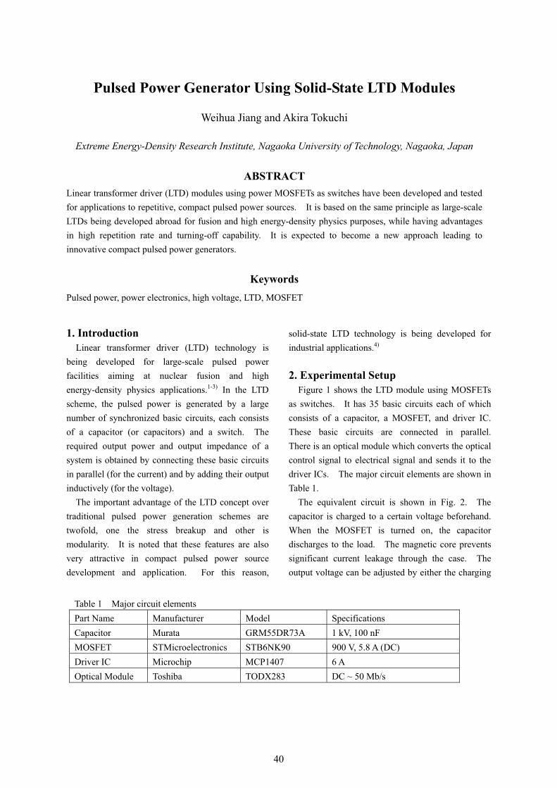
Table 1 Major circuit elements Part Name Manufacturer Model Specifications Capacitor Murata GRM55DR73A 1 kV, 100 nF MOSFET STMicroelectronics STB6NK90 900 V, 5.8 A (DC) Driver IC Microchip MCP1407 6 A Optical Module Toshiba TODX283 DC ~ 50 Mb/s
Pulsed Power Generator Using Solid-State LTD Modules
Weihua Jiang and Akira Tokuchi
Extreme Energy-Density Research Institute, Nagaoka University of Technology, Nagaoka, Japan
ABSTRACT Linear transformer driver (LTD) modules using power MOSFETs as switches have been developed and tested for applications to repetitive, compact pulsed power sources. It is based on the same principle as large-scale LTDs being developed abroad for fusion and high energy-density physics purposes, while having advantages in high repetition rate and turning-off capability. It is expected to become a new approach leading to innovative compact pulsed power generators.
Keywords
Pulsed power, power electronics, high voltage, LTD, MOSFET
1. Introduction Linear transformer driver (LTD) technology is being developed for large-scale pulsed power facilities aiming at nuclear fusion and high energy-density physics applications.1-3) In the LTD scheme, the pulsed power is generated by a large number of synchronized basic circuits, each consists of a capacitor (or capacitors) and a switch. The required output power and output impedance of a system is obtained by connecting these basic circuits in parallel (for the current) and by adding their output inductively (for the voltage). The important advantage of the LTD concept over traditional pulsed power generation schemes are twofold, one the stress breakup and other is modularity. It is noted that these features are also very attractive in compact pulsed power source development and application. For this reason,
solid-state LTD technology is being developed for industrial applications.4) 2. Experimental Setup Figure 1 shows the LTD module using MOSFETs as switches. It has 35 basic circuits each of which consists of a capacitor, a MOSFET, and driver IC. These basic circuits are connected in parallel. There is an optical module which converts the optical control signal to electrical signal and sends it to the driver ICs. The major circuit elements are shown in Table 1. The equivalent circuit is shown in Fig. 2. The capacitor is charged to a certain voltage beforehand. When the MOSFET is turned on, the capacitor discharges to the load. The magnetic core prevents significant current leakage through the case. The output voltage can be adjusted by either the charging
4040
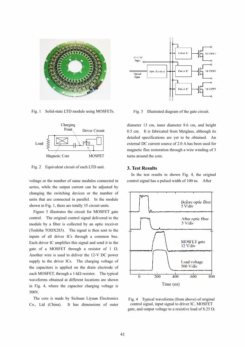
Fig. 1 Solid-state LTD module using MOSFETs.
Fig. 2 Equivalent circuit of each LTD unit.
Fig. 3 Illustrated diagram of the gate circuit.
voltage or the number of same modules connected in series, while the output current can be adjusted by changing the switching devices or the number of units that are connected in parallel. In the module shown in Fig. 1, there are totally 35 circuit units. Figure 3 illustrates the circuit for MOSFET gate control. The original control signal delivered to the module by a fiber is collected by an optic receiver (Toshiba TODX283). The signal is then sent to the inputs of all driver ICs through a common bus. Each driver IC amplifies this signal and send it to the gate of a MOSFET through a resistor of 1 �. Another wire is used to deliver the 12-V DC power supply to the driver ICs. The charging voltage of the capacitors is applied on the drain electrode of each MOSFET, through a 1-k� resistor. The typical waveforms obtained at different locations are shown in Fig. 4, where the capacitor charging voltage is 500V. The core is made by Sichuan Liyuan Electronics Co., Ltd (China). It has dimensions of outer
diameter 13 cm, inner diameter 8.6 cm, and height 0.5 cm. It is fabricated from Metglass, although its detailed specifications are yet to be obtained. An external DC current source of 2.0 A has been used for magnetic flux restoration through a wire winding of 3 turns around the core. 3. Test Results In the test results in shown Fig. 4, the original control signal has a pulsed width of 100 ns. After
Fig. 4 Typical waveforms (from above) of original control signal, input signal to driver IC, MOSFET
gate, and output voltage to a resistive load of 8.25 �.
4141
Fig. 5 LTD-based pulsed power generator
using 5 modules shown in Fig. 1.
0 100 200 300
0
1
2
3
4
5
Time (ns)
Load
Vol
tage
(kV
)
Rload = 12.5 �
Fig. 6 Output voltage from a 5-module LTD
generator to resistive load of 12.5 �.
the optical transmission, the signal is delayed for only
a few nanoseconds and the pulse width is about the
same. However, a ~100 ns delay is caused by the
driver IC which also causes a slight increase in pulse
length. The output waveform clearly followed that
of the driver IC.
Figure 5 shows the 5-module LTD assemble. It
has been tested with charging voltage of 800 V. The
output voltage form obtained on a resistive load of
12.5 � is shown in Fig. 6. The peak voltage reaches
nearly 4 kV, with a rise-time of ~ 20 ns and a
fall-time of ~ 40 ns, and a pulse width (FWHM) of ~
120 ns. The peak output current is calculated to be
~ 320 A giving a peak output power of ~ 1.3 MW.
The repetition rate for this testing operation was 1
kHz (continuous).
4. Conclusions A 5-module LTD assembly has been developed and tested, in order to demonstrate the effectiveness of LTD concept in pulsed power generation. Output of 4 kV with pulsed length of ~ 120 ns has been obtained at repetition rate of 1 kHz. References [1] B. M. Koval’chuk, V. A. Vizir’, A. A. Kim, E. V.
Kumpyak, S. V. Loginov, A. N. Bastrikov, V. V. Chervyakov, N. V. Tsoi, P. Monjaux, and D. Kh’yui, “Fast Primary Storage Device Utilizing A Linear Pulse Transformer”, Russian Physics Journal, vol. 40, no. 12, pp. 1142-1153, 1997.
[2] M. G. Mazarakis, W. E. Fowler, A. A. Kim, V. A. Sinebryukhov, S. T. Rogowski, R. A. Sharpe, D. H. McDaniel, C. L. Olson, J. L. Porter, K. W. Struve, W. A. Stygar, and J. R. Woodworth, “High Current, 0.5-MA, Fast, 100-ns, Linear Transformer Driver Experiments”, Physical Review Special Topics – Accelerators and Beams, vol. 12, 050401-1~17, 2009.
[3] W. A. Stygar, M. E. Cuneo, D. I. Headley, H. C. Ives, R. J. Leeper, M. G. Mazarakis, C. L. Olson, J. L. Porter, T. C. Wagoner, and J. R. Woodworth, “Architecture of Petawatt-Class Z-Pinch Accelerators”, Physical Review Special Topics – Accelerators and Beams, vol. 10, 030401-1~24, 2007.
[4] W. Jiang: “Solid-State LTD Module Using Power MOSFETs”, IEEE Transactions on Plasma Science, vol. 38, no. 10, 2730-2733, 2010.
4242
DEVELOPMENT OF MOS-FET BASED MARX GENERATOR WITH SELF-PROVED GATE POWER
A. Tokuchi1,2,3, W. Jiang2, K. Takayama3, T. Arai3, T. Kawakubo3 and T. Adachi3
1Pulsed Power Japan Laboratory Ltd., Kusatsu, Shiga, 525-0027, Japan
2Nagaoka University of Technology, Nagaoka, Niigata, 525-0027, Japan
3High Energy Accelerator Research Organization (KEK), Tsukuba, Ibaraki 305-0801, Japan
ABSTRACT
New MOS-FET based Marx generator is described. An electric gate power for the MOS-FET is provided from the Marx main circuit itself. Four-stage Marx generator generates -12kV of the output voltage. The Marx Generator is successfully used to drive an Einzel lens chopper to generate a short pulsed ion beam for a KEK digital accelerator.
1. Introduction For many years, A Marx circuit was used to
generate a high voltage pulse. Figure 1 shows a conventional Marx circuit. All capacitors ( C1~CN ) are charged in parallel through charging resistors up to a voltage of Vc. After finishing the charging, all spark gap switches are closed the circuit by an external trigger pulse, then all capacitors are connected in series and a high voltage pulse of NVc is generated. Here, N is a number of the capacitors. There are some demerits in the conventional Marx circuit as follows. � Long charging time because the charging
current flows through the charging resistors. � Low efficiency because of the same reason
mentioned above. � Low repetition rate because of the same
reason.� Few output voltage appearance in charging
period because the charging current flows through the charging resistors and a load.
� Turn-off is impossible because of using the spark gap switches.
� Short life time of the spark gap switches. In order to solve these problems, some new Marx
circuits are proposed. These new improved circuits use semiconductor switches such as MOS-FETs or IGBTs. Two types of the improved circuits are introduced here. Figure 2 shows an improved Marx circuit that we
called TYPE-1. In the TYPE-1 circuit, all charging resistors are replaced to diodes and all spark gap switches are replaced to semiconductor switches. In fig. 2, MOS-FETs are used as semiconductor
Figure 1: Conventional Marx circuit.
switches. In The TYPE-1 circuit, some demerits of conventional Marx circuit are improved as follows. � Relatively short charging time because the
charging current flows through the diodes instead of the charging resistors.
� Relatively high efficiency because of the same reason mentioned above.
� Reletively high repetition rate because of the same reason.
� Turn-off is possible because of using the semiconductor switches instead of the spark gap switches.
� Long life time of the switches. But some demerits and new demerit are still remained in the TYPE-1 circuit as follows. � Few output voltage appearance in charging
period because the charging current flows through a load.
� About the chrging time, the efficiency and the repetition rate, they are not optimal because
4343
of above-mentioned reason. � One additional gate circuit is required in each
Marx stage to drive the semiconductor switch.
Figure 2: Improved Marx circuit (TYPE-1).
To the next, fig. 3 shows an improved Marx circuit that we called TYPE-2. In the TYPE-2 circuit, a half of the charging diodes are replaced to another semiconductor switches. In fig. 3, MOS-FETs are also used as the second semiconductor switches. In The TYPE-2 circuit, all demerits of conventional Marx circuit are further improved as follows. � Very short charging time because of no
charging resistor in charging circuit. � Very high efficiency because of the same
reason mentioned above. � Very high repetition rate because of the same
reason.� Turn-off is possible because of using the
semiconductor switches. � Long life time of the switches. � No output voltage appearance in charging
period because the charging current dose not flow a load.
But new demerit of the TYPE-2 circuit is described as follows. � Two additional gate circuits are required in
each Marx stage to drive the semiconductor switch.
Figure 3: Improved Marx circuit (TYPE-2).
We developed TYPE-1 Marx circuit in order to drive an Einzel lens chopper used for a short pulsed ion beam generation to inject into a digital accelerator
at KEK.
2. A design of a Marx board Table 1 shows target specifications of the
developed Marx board. Four Marx-boards were used to generate an output pulsed voltage of 12kV.
Table 1 Specifications of the Marx board. Switching device MOS-FET
IXTF1N400(IXYS) Rationg:4kV,1A,3Ap
Circuit configuration Improved Marx circuit (TYPE-1) Involving a dummy load
Charging voltage 3kV Pulse output current 9Ap Gate power supply Self-providing from
main circuit Rise time Less than 30ns
In case of the Marx circuit using semiconductor switch, an important technical problem is how to provide a gate power to drive the semiconductor switches. Each Marx board is triggered by optical fiber signal, because a voltage potential of the each Marx board is different each other. An electric power supply is required to transmit from optical trigger signal to electric gate signal in each Marx board. There are following three methods to provide the electric gate power to the Marx board.
(1) Using DC-DC converter (2) Using isolation transformer and AC-DC
converter (3) Self-providing from main circuit
In case of (1), an isolation voltage of the commercial DC-DC converter is less than about 6kV. Therefore a high voltage pulse generator cannot use this method. In case of (2), a stray capacitance of the isolation transformer may cause a serious oscillation of the output pulsed voltage, and it is usually difficult to find out optimal devices in commercial. In case of (3), a technical problem is how to reduce a current from main circuit to the gate circuit. In this development we chose a method of (3). Figure 4 shows a circuit diagram to provide a electric gate power from a main circuit of the Marx circuit. A
Figure 4: Circuit diagram to provide gate power from main circuit.
4444
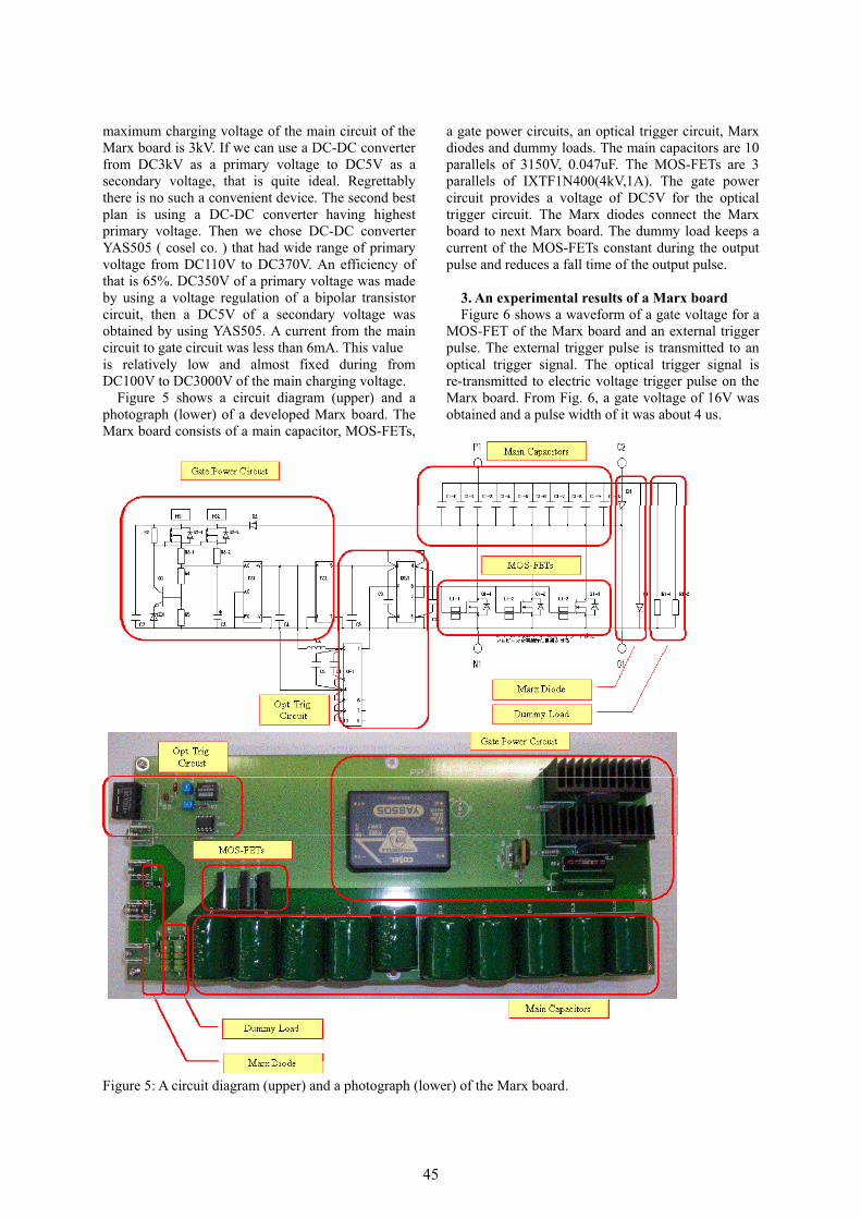
maximum charging voltage of the main circuit of the Marx board is 3kV. If we can use a DC-DC converter from DC3kV as a primary voltage to DC5V as a secondary voltage, that is quite ideal. Regrettably there is no such a convenient device. The second best plan is using a DC-DC converter having highest primary voltage. Then we chose DC-DC converter YAS505 ( cosel co. ) that had wide range of primary voltage from DC110V to DC370V. An efficiency of that is 65%. DC350V of a primary voltage was made by using a voltage regulation of a bipolar transistor circuit, then a DC5V of a secondary voltage was obtained by using YAS505. A current from the main circuit to gate circuit was less than 6mA. This value is relatively low and almost fixed during from DC100V to DC3000V of the main charging voltage.
Figure 5 shows a circuit diagram (upper) and a photograph (lower) of a developed Marx board. The Marx board consists of a main capacitor, MOS-FETs,
a gate power circuits, an optical trigger circuit, Marx diodes and dummy loads. The main capacitors are 10 parallels of 3150V, 0.047uF. The MOS-FETs are 3 parallels of IXTF1N400(4kV,1A). The gate power circuit provides a voltage of DC5V for the optical trigger circuit. The Marx diodes connect the Marx board to next Marx board. The dummy load keeps a current of the MOS-FETs constant during the output pulse and reduces a fall time of the output pulse.
3. An experimental results of a Marx board Figure 6 shows a waveform of a gate voltage for a
MOS-FET of the Marx board and an external trigger pulse. The external trigger pulse is transmitted to an optical trigger signal. The optical trigger signal is re-transmitted to electric voltage trigger pulse on the Marx board. From Fig. 6, a gate voltage of 16V was obtained and a pulse width of it was about 4 us.
Figure 5: A circuit diagram (upper) and a photograph (lower) of the Marx board.
4545
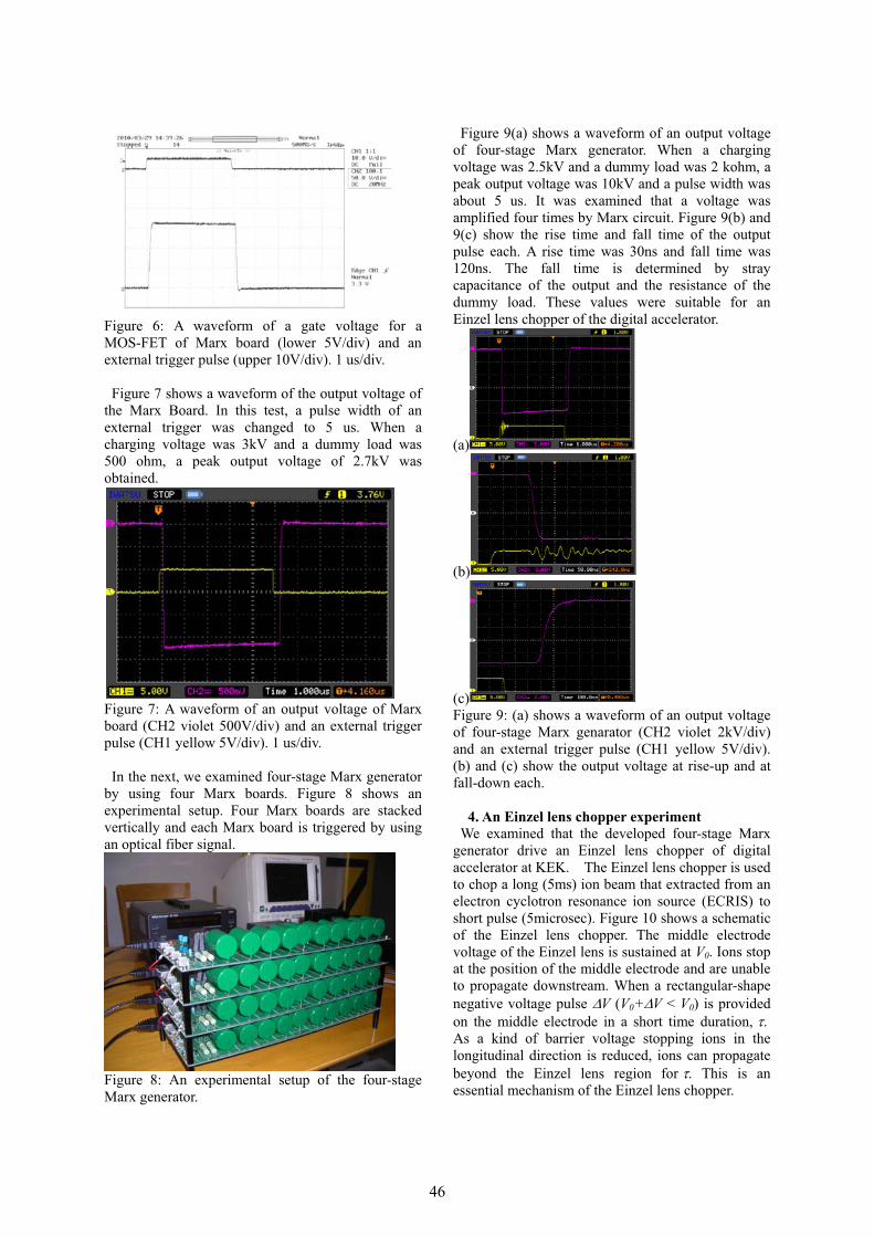
Figure 6: A waveform of a gate voltage for a MOS-FET of Marx board (lower 5V/div) and an external trigger pulse (upper 10V/div). 1 us/div.
Figure 7 shows a waveform of the output voltage of the Marx Board. In this test, a pulse width of an external trigger was changed to 5 us. When a charging voltage was 3kV and a dummy load was 500 ohm, a peak output voltage of 2.7kV was obtained.
Figure 7: A waveform of an output voltage of Marx board (CH2 violet 500V/div) and an external trigger pulse (CH1 yellow 5V/div). 1 us/div.
In the next, we examined four-stage Marx generator by using four Marx boards. Figure 8 shows an experimental setup. Four Marx boards are stacked vertically and each Marx board is triggered by using an optical fiber signal.
Figure 8: An experimental setup of the four-stage Marx generator.
Figure 9(a) shows a waveform of an output voltage of four-stage Marx generator. When a charging voltage was 2.5kV and a dummy load was 2 kohm, a peak output voltage was 10kV and a pulse width was about 5 us. It was examined that a voltage was amplified four times by Marx circuit. Figure 9(b) and 9(c) show the rise time and fall time of the output pulse each. A rise time was 30ns and fall time was 120ns. The fall time is determined by stray capacitance of the output and the resistance of the dummy load. These values were suitable for an Einzel lens chopper of the digital accelerator.
(a)
(b)
(c) Figure 9: (a) shows a waveform of an output voltage of four-stage Marx genarator (CH2 violet 2kV/div) and an external trigger pulse (CH1 yellow 5V/div). (b) and (c) show the output voltage at rise-up and at fall-down each.
4. An Einzel lens chopper experiment We examined that the developed four-stage Marx
generator drive an Einzel lens chopper of digital accelerator at KEK. The Einzel lens chopper is used to chop a long (5ms) ion beam that extracted from an electron cyclotron resonance ion source (ECRIS) to short pulse (5microsec). Figure 10 shows a schematic of the Einzel lens chopper. The middle electrode voltage of the Einzel lens is sustained at V0. Ions stop at the position of the middle electrode and are unable to propagate downstream. When a rectangular-shape negative voltage pulse �V (V0+�V < V0) is provided on the middle electrode in a short time duration,����As a kind of barrier voltage stopping ions in the longitudinal direction is reduced, ions can propagate beyond the Einzel lens region for��. This is an essential mechanism of the Einzel lens chopper.
4646
Figure 10: ECRIS with the extraction system and Einzel lens in the high voltage terminal.
Figure 11 show an experimental result of Einzel lens chopper. In the preliminary experiment, a pulse voltage of -8 kV and 5 �sec, which was generated by the Marx generator, was superimposed on the DC bias voltage of 14 kV at the middle electrode of the Einzel lens. The ion current of He2+ was monitored by a Faraday cap. The ion current pulse profile and the electrode voltage profile are shown in Fig. 7. In the time duration of the negative voltage pulse, the ion flow arrived at the Faraday cap. A reason of a delay time between the pulse voltage and the ion current pulse is a response of the Faraday cap. It was proved that the Einzel lens chopper driven by the MOS-FET based Marx generator successfully made the short ion beam from an ion beam extracted from slow ion source.
Figure 11: Experimental result of the Einzel lens chopper driven by the Marx generator. Negative voltage pulse (blue) and ion beam profile monitored by the Faraday cup (red).
5. summary A MOS-FET based Marx generator (TYPE-1) was
developed. A gate power was directly provided from the main circuit of Marx generator. A current flown from the main circuit to the gate circuit was about 6mA that was practically low. When the charging voltage was 3kV, an peak output voltage of 12kV was obtained by using Four-stage Marx generator. A rise time of the output voltage was 30ns. The MOS-FET based Marx generator was used to drive an Einzel lens chopper of a digital accelerator and successfully chopped to the short ion beam.
In near future, we will develop the next generation Marx generator (TYPE-2) and new gate power circuit using a combination of a high frequency inverter, a high voltage isolation transformer and a AC/DC converter.
A Marx generator using semiconductor switches has great advantages such as high repetition rate, high efficiency, small size, high reliability, easy control of an output voltage waveform and low cost. It is expected that the semiconductor Marx generator will be utilized for many new industrial applications.
References 1) T. Iwashita, T. Adachi, K. Takayama, T. Arai, Y.
Arakida, M. Hashimoto, E. Kadokura, M. Kawai, T. Kawakubo, Tomio Kubo, K. Koyama, H.Nakanishi, K. Okazaki, K. Okamura, H. Someya, A. Takagi, A. Tokuchi, K. W. Leo, and M. Wake, “KEK Digital Accelerator”, to be published in Phys. Rev. ST-AB 14, 071301 (2011).
2) Toshikazu Adachi, Teruo Arai, Kwee Wah Leo, Ken Takayama, and Akira Tokuchi, "A Solid-state Marx Generator Driven Einzel Lens Chopper", Rev. of Sci. Inst. 82, 083305 (2011).
4747
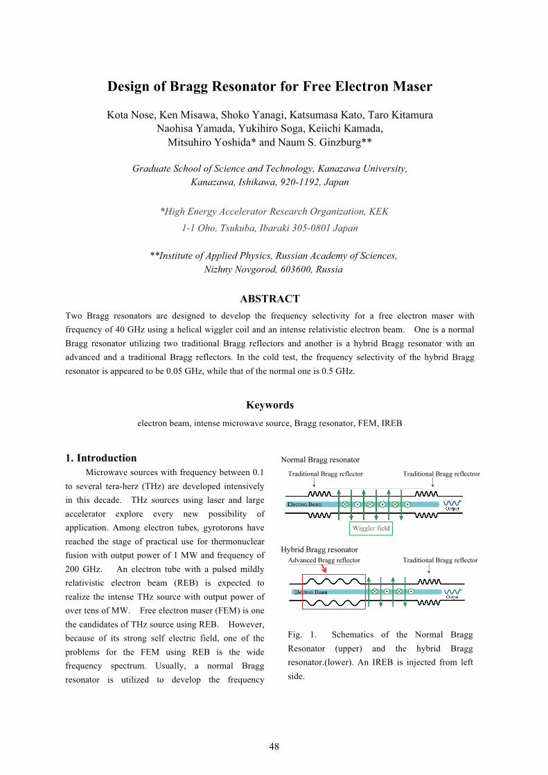
Design of Bragg Resonator for Free Electron Maser
Kota Nose, Ken Misawa, Shoko Yanagi, Katsumasa Kato, Taro Kitamura Naohisa Yamada, Yukihiro Soga, Keiichi Kamada,
Mitsuhiro Yoshida* and Naum S. Ginzburg**
Graduate School of Science and Technology, Kanazawa University, Kanazawa, Ishikawa, 920-1192, Japan
*High Energy Accelerator Research Organization, KEK
1-1 Oho, Tsukuba, Ibaraki 305-0801 Japan
**Institute of Applied Physics, Russian Academy of Sciences, Nizhny Novgorod, 603600, Russia
ABSTRACT Two Bragg resonators are designed to develop the frequency selectivity for a free electron maser with frequency of 40 GHz using a helical wiggler coil and an intense relativistic electron beam. One is a normal Bragg resonator utilizing two traditional Bragg reflectors and another is a hybrid Bragg resonator with an advanced and a traditional Bragg reflectors. In the cold test, the frequency selectivity of the hybrid Bragg resonator is appeared to be 0.05 GHz, while that of the normal one is 0.5 GHz.
Keywords
electron beam, intense microwave source, Bragg resonator, FEM, IREB
1. Introduction Microwave sources with frequency between 0.1
to several tera-herz (THz) are developed intensively in this decade. THz sources using laser and large accelerator explore every new possibility of application. Among electron tubes, gyrotorons have reached the stage of practical use for thermonuclear fusion with output power of 1 MW and frequency of 200 GHz. An electron tube with a pulsed mildly relativistic electron beam (REB) is expected to realize the intense THz source with output power of over tens of MW. Free electron maser (FEM) is one the candidates of THz source using REB. However, because of its strong self electric field, one of the problems for the FEM using REB is the wide frequency spectrum. Usually, a normal Bragg resonator is utilized to develop the frequency
Fig. 1. Schematics of the Normal Bragg Resonator (upper) and the hybrid Bragg resonator.(lower). An IREB is injected from left side.
4848
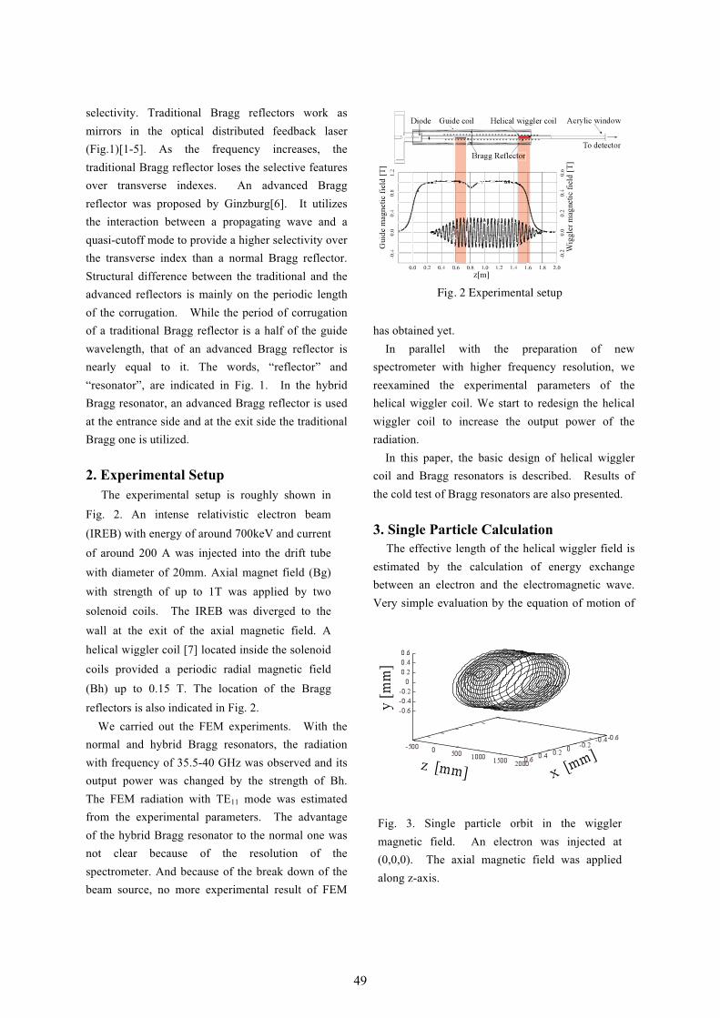
selectivity. Traditional Bragg reflectors work as mirrors in the optical distributed feedback laser (Fig.1)[1-5]. As the frequency increases, the traditional Bragg reflector loses the selective features over transverse indexes. An advanced Bragg reflector was proposed by Ginzburg[6]. It utilizes the interaction between a propagating wave and a quasi-cutoff mode to provide a higher selectivity over the transverse index than a normal Bragg reflector. Structural difference between the traditional and the advanced reflectors is mainly on the periodic length of the corrugation. While the period of corrugation of a traditional Bragg reflector is a half of the guide wavelength, that of an advanced Bragg reflector is nearly equal to it. The words, “reflector” and “resonator”, are indicated in Fig. 1. In the hybrid Bragg resonator, an advanced Bragg reflector is used at the entrance side and at the exit side the traditional Bragg one is utilized.
2. Experimental Setup The experimental setup is roughly shown in
Fig. 2. An intense relativistic electron beam (IREB) with energy of around 700keV and current of around 200 A was injected into the drift tube with diameter of 20mm. Axial magnet field (Bg) with strength of up to 1T was applied by two solenoid coils. The IREB was diverged to the wall at the exit of the axial magnetic field. A helical wiggler coil [7] located inside the solenoid coils provided a periodic radial magnetic field (Bh) up to 0.15 T. The location of the Bragg reflectors is also indicated in Fig. 2. We carried out the FEM experiments. With the normal and hybrid Bragg resonators, the radiation with frequency of 35.5-40 GHz was observed and its output power was changed by the strength of Bh. The FEM radiation with TE11 mode was estimated from the experimental parameters. The advantage of the hybrid Bragg resonator to the normal one was not clear because of the resolution of the spectrometer. And because of the break down of the beam source, no more experimental result of FEM
has obtained yet. In parallel with the preparation of new spectrometer with higher frequency resolution, we reexamined the experimental parameters of the helical wiggler coil. We start to redesign the helical wiggler coil to increase the output power of the radiation. In this paper, the basic design of helical wiggler coil and Bragg resonators is described. Results of the cold test of Bragg resonators are also presented. 3. Single Particle Calculation The effective length of the helical wiggler field is estimated by the calculation of energy exchange between an electron and the electromagnetic wave. Very simple evaluation by the equation of motion of
Fig. 3. Single particle orbit in the wiggler magnetic field. An electron was injected at (0,0,0). The axial magnetic field was applied along z-axis.
Fig. 2 Experimental setup
4949
an electron was employed. An electron was injected into the axial and helical magnetic field with the electromagnetic wave. The typical orbit of an electron without the electromagnetic wave is shown
in Fig. 3. A helical orbit whose period is equal to that of the helical coil is observed. Without the gradual increase of the helical wiggler field, electrons hit the wall. The increase or decrease of the kinetic energy of an electron travelling with electromagnetic wave through the magnetic fields was evaluated along the axis. The initial phase of the electromagnetic wave at the injection point of an electron was varied from 0 to 2π. The sum of the kinetic energy difference of electrons injected at different initial phase was calculated along the axial length. It was supposed that the decrease of the kinetic energy of electrons was equal to the increase of the energy of the electromagnetic wave. But the latter increase was not reflected to the calculation. Figure 4 show the energy increase/decrease of the beam electrons propagating with the electromagnetic wave with frequency of 40 GHz. The maximum energy decrease is observed at the electron energy of 630 keV. The intersection point of the beam and TE11 mode lines of the dispersion relation is 620 keV, 40 GHz where the phase velocities of the beam and TE11 mode are the same. At this point, the exchange of the energy is zero as shown in Fig.3 as expected. We use the results of the single particle calculation as rough criteria to design the helical wiggler coil and beam radius. Figure 5 shows the energy decrease of the electrons along the axial length of the helical wiggler coil. It is clear that the energy decrease is saturated at z=200 cm i.e. 40 pitches of the wiggler coil. It is also calculated that the energy decrease of the electrons reduces with the distance from the axis (Fig. 6). This can be used to determine the beam radius. The energy exchange between the backward wave and electrons was calculated as the energy exchange by the reflected wave from the Bragg reflector at the downstream side was anticipated. The energy of electrons was not changed by the backward wave. 4. Bragg resonators 4.1 Design and cold test of Bragg reflectors
Fig. 6. Energy decrease of electrons vs the
initial radial position of electrons.
Fig. 4. Energy decrease of electrons propagating with 40 GHz, TE11 electromagnetic wave through drift tube immersed in the wiggler and axial magnetic field.
Fig. 5. Energy decrease of electrons vs the
wiggler length.
5050

The period of corrugation for a traditional Bragg reflector can be determined by the relation kg=kb/2, where kg is the wave number for 40 GHz, TE11 mode of the circular waveguide and kb is that of the corrugation period. To determine the depth of the corrugation and the length of the traditional reflector, we use the simulation code CST MW studio. Before we utilized the simulation, we check the reliability of the simulation. The reflective coefficient of the traditional Bragg reflector was calculated by use of the Mode-coupling theory [8]. In the calculation, the frequency of 40 GHz (TE11 mode) is expected and TM11 mode is considered to be a candidate of mode conversion. The calculated results showed good agreement with the simulated one as shown in Fig. 7.
The simulated results of reflective coefficient for the depth and the total length of the corrugation for the traditional Bragg reflector are sown in Fig. 8. From these results, the depth and total length are decided to be 0.25 mm and 400 mm, respectively. We applied the simulated results to set the parameters of an advanced Bragg reflector. The parameters of both Bragg reflectors are summarized on Table 1. The reflective coefficient of the 40 GHz advanced Bragg reflector is also plotted in Fig. 7
along the frequency. The width of the frequency peak of the advanced Bragg reflector is nearly 10 times narrower than the traditional one. Traditional Advanced Mode TE11 TE11
Frequency [GHz] 39.8 39.8
Frequency Width [GHz]
0.5 0.05
Corrugation
Period [mm] 3.9 7.6
Depth [mm] 0.25 0.1
Length [mm] 400 200
Table 1 Parameters of traditional and advanced
Bragg reflectors
Fig. 7. Calculated results based on the mode coupling theory and simulated results for the traditional Bragg reflector show good agreement. The simulated results of the advanced Bragg reflector is also shown.
Fig. 8. Simulated results of reflective coefficient vs depth (upper) and length (lower) for the traditional Bragg reflector
5151
Cold tests of the Bragg reflectors were carried out using network analyzer E8354C (Agilent Technology). The microwave passed through the Bragg reflector was detected. The experimental results show good agreements with the simulated results as shown in Fig.9. The width of the reflected frequency of the advanced Bragg reflector is about 10 times narrower than that of the traditional one. This result should contribute to higher frequency selectivity of the hybrid Bragg resonator than that of the normal one.
4.2 Cold test of Bragg resonators Cold tests for normal and hybrid Bragg resonators were carried out with the same network analyzer used for Bragg reflectors. Microwave with frequency around 40 GHz was radiated at the center of the Bragg resonator. And the microwave passed through the traditional Bragg reflector located at the downstream side of both resonators was detected as shown in Fig. 10. The experimental result of the normal Bragg resonator is shown in Fig. 11. Several peaks were observed within the frequency range in which the microwave passed through the traditional Bragg reflector. The frequencies of each peak are the function of the distance between two Bragg reflectors. The frequency spectrum passed through the hybrid Bragg resonator is shown in Fig. 12. A single
narrow peak is observed at the detected frequency of the advanced Bragg reflector. In comparison with the cold test of the normal Bragg resonator, we can expect the higher frequency selectivity of the hybrid Bragg resonator. We will carry out the further experiments to increase the output power of the hybrid Bragg
Fig. 9. Transparent characteristics of normal and
advanced Bragg reflectors (cold test).
Fig.10. Schematic of the cold test of Bragg
resonators.
Fig. 12. Frequency spectrum of the hybrid
Bragg resonator.
Fig. 11. Frequency spectrum of the normal
Bragg resonator.
5252
resonator and the appropriate distance between the Bragg reflectors. 4. Conclusions Criteria of the design of the wiggler coil and beam radius for more intense radiation were obtained by the single particle calculation of the energy exchange between electrons and electromagnetic wave. The simulated and experimental results of the traditional and the advanced Bragg reflectors show good agreements. We can design new Bragg resonators by the simulation. From the results of the cold test of both Bragg resonators, we can expect higher frequency selectivity of the hybrid Bragg resonator than the normal one. References [1] A. Kasugai, K. Sakamoto, K. Takahashi, K.
Kajiwara and N. Kobayashi: "Steady-state operation of 170 GHz–1 MW gyrotron for ITER", Nuclear Fusion, Vol. 48, Issue 5, pp. 054009 (2008).
[2] G. G. Denisov, M. G. Reznikov: "Corrugated cylindrical resonators for short-wavelength relativistic microwave oscillators ", Radiophysics and Quantum Electronics, vol. 25, No 5, pp. 407-413, (1982).
[3] R. B. Mccowan: “Design of a waveguide resonator with rippled wall reflectors for a 100 GHz CARM oscillator”, Int. J. Electronics, Vol.65, No.3, pp. 463-475, (1988).
[4] I. Boscolo: “A tunable Bragg cavity for an efficient millimeter FEL driven by electrostatic accelerators”, Appl. Phys. B57, pp. 217-225, (1993)
[5] T. S. Chu, F. V. Hartemann, B. G. Danly, and R. J. Temkin: “Single-Mode Operation of a Bragg Free-Electron Maser Oscillator”, Phys. Rev. Lett., 72, 2391-2394 (1994)
[6] N. S. Ginzburg, A. M. Malkin, N. Yu. Peskov, A. S. Sergeev, A. K. Kaminsky, S. N. Sedykh,
E. A. Perelshtein, A. P. Sergeev, A. V. Elzhov: "Improving selectivity of free electron maser with 1D Bragg resonator using coupling of propagating and trapped waves", Phys. Rev. ST-AB, vol. 8, 040705, (2005).
[7] K. T. McDonald:“The Helical Wiggler” Joseph Henry Laboratory Princeton UniversityPrinceton NJ 08544 Oct.12. (1986).
[8] N. S. Ginzburg, A. M. Malkin, N. Yu. Peskov, A. S. Sergeev, V. Yu. Zaslavsky, K. Kamada, R. Ando: "Free electron laser with terahertz band Bragg reflectors", Phys. Rev. ST-AB, vol. 12, 060702, (2009).
[9] N. S. Ginzburg, A. M. Malkin, N. Yu. Peskov, A. S. Sergeev, V. Yu. Zaslavsky, K. Kamada, Y. Soga: "Tunable terahertz band planar Bragg reflectors", Appl. Phys. Lett. 95, 043504, (2009).
[10] N. Ginzburg, A. Malkin, N. Peskov, A. S. Sergeev, V. Zaslavsky, I. Zotova, K. Kamada, Y. Soga: "Terahertz band FEL with advanced Bragg Reflectors", Proc. of FEL conf., Liverpool, UK., pp. 424-427, (2009).
5353
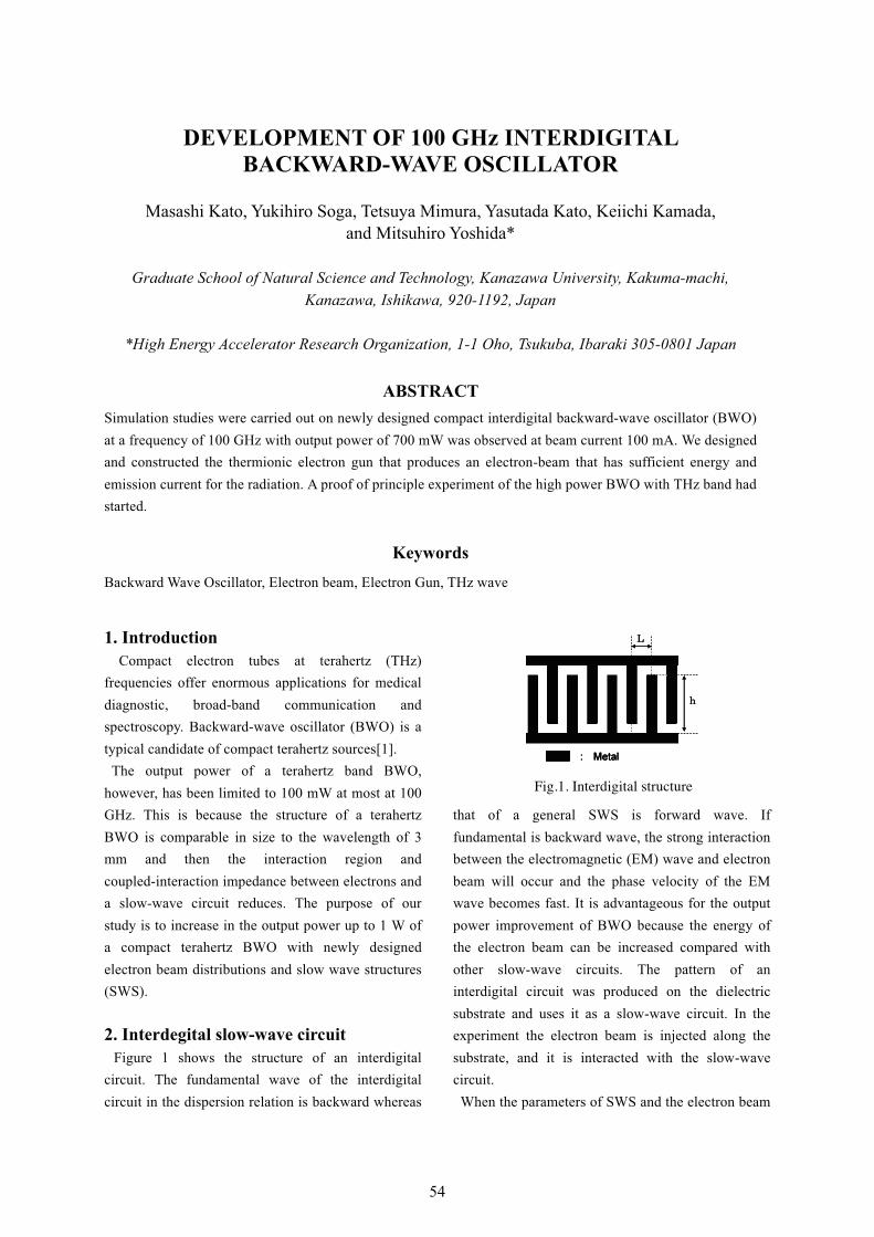
DEVELOPMENT OF 100 GHz INTERDIGITAL BACKWARD-WAVE OSCILLATOR
Masashi Kato, Yukihiro Soga, Tetsuya Mimura, Yasutada Kato, Keiichi Kamada,
and Mitsuhiro Yoshida*
Graduate School of Natural Science and Technology, Kanazawa University, Kakuma-machi, Kanazawa, Ishikawa, 920-1192, Japan
*High Energy Accelerator Research Organization, 1-1 Oho, Tsukuba, Ibaraki 305-0801 Japan
ABSTRACT Simulation studies were carried out on newly designed compact interdigital backward-wave oscillator (BWO) at a frequency of 100 GHz with output power of 700 mW was observed at beam current 100 mA. We designed and constructed the thermionic electron gun that produces an electron-beam that has sufficient energy and emission current for the radiation. A proof of principle experiment of the high power BWO with THz band had started.
Keywords
Backward Wave Oscillator, Electron beam, Electron Gun, THz wave
1. Introduction Compact electron tubes at terahertz (THz) frequencies offer enormous applications for medical diagnostic, broad-band communication and spectroscopy. Backward-wave oscillator (BWO) is a typical candidate of compact terahertz sources[1]. The output power of a terahertz band BWO, however, has been limited to 100 mW at most at 100 GHz. This is because the structure of a terahertz BWO is comparable in size to the wavelength of 3 mm and then the interaction region and coupled-interaction impedance between electrons and a slow-wave circuit reduces. The purpose of our study is to increase in the output power up to 1 W of a compact terahertz BWO with newly designed electron beam distributions and slow wave structures (SWS). 2. Interdegital slow-wave circuit Figure 1 shows the structure of an interdigital circuit. The fundamental wave of the interdigital circuit in the dispersion relation is backward whereas
that of a general SWS is forward wave. If fundamental is backward wave, the strong interaction between the electromagnetic (EM) wave and electron beam will occur and the phase velocity of the EM wave becomes fast. It is advantageous for the output power improvement of BWO because the energy of the electron beam can be increased compared with other slow-wave circuits. The pattern of an interdigital circuit was produced on the dielectric substrate and uses it as a slow-wave circuit. In the experiment the electron beam is injected along the substrate, and it is interacted with the slow-wave circuit. When the parameters of SWS and the electron beam
Fig.1. Interdigital structure
5454
are determined, it is needed to estimate the radiation frequency from the intersection of the dispersion curve of the EM wave propagating on SWS and the beam mode. In this analysis the dispersion of the interdigital type slow-wave circuit is considered. Because the EM wave propagates between the combs of metal, the relation between the phase �BW and the frequency � can be written as �BW = (h + L)� /vg �� . (1)
Here h is the height of the comb teeth, L is the length of one pitch (Fig.1) and vg is a group velocity of the EM wave and then vg = c �eff . (2)
Here �eff is an effective permittivity of the
dielectric substrate. Because the mode of EM wave on the SWS is almost the same as the quasi-TEM mode that propagates on the coplanar stripline, �eff may be written as follows
�eff = 1 +�r �1
2
K (k' )K (k1)
K (k)K (k1' ), (3)
where K is complete elliptic integral of the first kind and
k = a /b , k1 =sinh(�a / 2d)
sinh(�b / 2d), a = S / 2, b = S / 2 +W
k' = 1� k 2 ,
where S is the width of metal, W is the distance between the gap and d is the thickness of dielectric. The interdigital slow-wave circuit is designed by using the equations (1) - (3) that can radiate the EM wave at a frequency 100GHz for the electron beam with the energy of 10keV. The dielectric substrate is made from 1 mm thickness Teflon (relative permittivity is equal to 2). Table 1 shows the designed parameters of SWS.
Table.1 Parameters of SWS
Figure 2 shows the dispersion relation of the
slow-wave circuit in the determined parameters. The radiation is expected at the frequency on the intersection with the beam mode in the dispersion. However, the dispersion lines will actually bend where the wave number is 0 and because the impedance change for the frequency is not considered in Fig.2.
3. Simulation on EM wave radiation We calculated an EM wave radiation from the designed interdigital slow-wave circuit using CST PARTICLE STUDIO in CST STUDIO SUITE. This is one of the most commonly used software in the field of accelerator or microwave tubes [2,3]. Figure 3 shows the position of the slow-wave circuit and the electron beam. The cylindrical electron beam is injected along the surface of the slow-wave circuit on the substrate. The diameter of the cathode is 1 mm, and the distance between the SWS and the bottom of the electron beam is 0.1 mm.
The metal of SWS is made of copper. The EM radiation generated in the slow-wave circuit is
Thickness of metal 20 μm
Thickness of substrate 1 mm
L 150 μm
h 440 μm
Number of pitch 200
Fig.2. Dispersion of interdigital circuit
Fig.3. Schematic view of slow-wave circuit
and electron beam
5555
observed in the port indicated by a square under the left in Fig. 3 connected with the coplanar stripline on the cathode side. The expected mode of EM wave received in the port is a quasi-TEM mode, and the electric field distribution is shown in Fig. 4.
In this simulation it is assumed that the electron beam is emitted from the surface of the cathode along the axis with an equal energy of 10 keV, and the current is from 50 to 100 mA (5 – 10 A/cm2). The axial magnetic field to prevent the electron beam from being scattered is generated with the doughnut type neodymium magnet of 15 mm in the inside diameter, 30mm in the outside diameter, and 40mm in the axial length. An almost homogeneous axial magnetic field of 0.17 to 0.2 T can be obtained by this magnet as shown in Fig. 5. Figure 6 shows the signal of the EM wave observed at the port when the beam current is 100 mA. The signal begins to increase at about 8 ns after the injection of the beam, and a steady radiation is achieved in 14 ns. The output power at the steady state is 700mW. A FFT analysis shown in the lower
graph of Fig. 6 indicates the signal of the port is a single spectrum at a frequency of 102GHz. This frequency is corresponding to that expected from the intersection of the beam mode and the dispersion of the slow-wave circuit.
Fig.6. A signal at the port and FFT analysis
Figure 7 represents a typical energy distribution of the electron beam during the steady radiation. A bunch of electrons corresponding to the fundamental period of the slow-wave circuit is formed as a result of the interaction with the EM radiation. Only a vicinity of the electron beam near the SWS can interact with the EM wave.
Fig.7. Energy distribution of electrons during radiation
The output power of a radiation when the beam current is changed from 50 to 100 mA is plotted in Fig. 8. The almost linear increase of output power as the injection power of electrons increases suggests
Fig.4. Distribution of electric field at the port
Fig.5. Distribution of magnetic field along the axis
-1
-0.8
-0.6
-0.4
-0.2
0
0.2
0.4
0.6
0.8
0 2 4 6 8 10 12 14 16
E-f
ield
[a.u
.]
Time [nsec]
signal
0
0.02
0.04
0.06
0.08
0.1
0.12
0 20 40 60 80 100 120 140 160
Inte
nsity
[a.u
.]
Frequency [GHz]
FFT of signal
5656
that the ratio of the interactive part of the electrons is unchanged. A radiation is not observed in the current of 50 mA because of the lack of the simulation time (up to 100 ns) or the joule loss in the slow-wave circuit. Moreover the start time decreases as the current increases. The large current contributes to the intense radiation due to the strong coupling to the EM wave. To obtain the radiation in this slow-wave circuit under the present condition, the electron current of more than 60 mA (the current density of about 6 A/cm2) is required.
4. Experimental test of electron gun The designed electron gun was experimentally evaluated. We used Ir coated impregnated cathode as the emitter [4]. The schematic experimental device is shown in Fig. 9. The electrons that flow into the drift space are received with the collector, and the observation currents are plotted in Fig. 10. The maximum total current of 3.3 mA is observed at 650 V in the acceleration voltage. The currents are proportional to the 1.6th power of the acceleration voltage. This result suggests that the current is limited by the space charge. The electron beam that has flowed into the drift space is about 65 % of the total current. This is because the electron beam is absorbed to the anode due to misalignment of the magnet, the cathode, and the anode. It is important to inject the electron-beam with an enough constant current density into the interacting region in order to get a steady radiation of BWO. Because the strong magnetic field guides beam to the axial direction, the current density doesn't change greatly even if the 35 % of the beam hits the anode in
our electron gun. The result of current measurements suggests that the electron-beam obtained by the electron gun has sufficient energy and emission current density for the radiation.
5. Conclusions We designed interdigital BWO at a frequency of 100GHz for the electron beam of 10 keV. The particle simulation using CST studio showed that when the electron-beam of 10kV in the acceleration voltage and the current 100mA is injected, the EM radiation of frequency 102GHz with output power of 700mW was observed. This is about five times larger than the present BWO with a same range. An experimental evaluation was carried out about the designed thermionic electron gun. We confirmed the electron-beam emitted from the electron gun has sufficient energy and emission current for the radiation. References [1] G. Kantorowicz and P. Palluel, “Backward Wave
Fig.8. Current vs output power and start time
Fig.9. Illustration of experimental device
Fig.10. Beam energy vs current in drift space
5757
Oscillators”, Infrared and Millimeter Waves, Vol.1 Sources of radiation, edited by K. J. Button pp.185-211 (1979).
[2] Carol L. Kory and James A. Dayton, Jr,
“Interaction Simulations of Two 650 GHz BWOs Using MAFIA”, Vacuum Electronics Conference, 2008. IVEC 2008. IEEE International, pp.390-391 (2008).
[3] Carol L. Kory and James A. Dayton, Jr, “Design
of 650 GHz Helical BWO Using CST Studio Suite”, Vacuum Electronics Conference, 2008. IVEC 2008. IEEE International, pp.392-393 (2008)
[4] S. Kimura, T. Yakabe, S. Matsumoto, D. Miyazaki,
T. Yoshii, M Fujiwara, and S. Koshigoe : “Ir-Coated Dispenser Cathode for CRT”, IEEE TRANSACTION ON ELECTRON DEVICES, Vol.37, No.12 pp.2564-2567 (1990)
5858
Longitudinal Bunch Compression Study with Induction Voltage Modulator
Akira Nakayama1, Yoshifumi Miyazaki1, Takashi Kikuchi2, Mitsuo Nakajima1, and Kazuhiko Horioka1∗1Department of Energy Sciences, Tokyo Institute of Technology,
Nagatsuta 4259, Midori-ku, Yokohama, 226-8502, Japan2Department of Electrical Engineering, Nagaoka University of Technology, 1603-1 Kamitomioka, Niigata 940-2188, Japan
For the beam driver of inertial confinement fusion, the technology to compress charged particlebeam in longitudinal direction is crucially important. However, the quality of the beam is expectedto be deteriorated when beam is rapidly compressed in the longitudinal direction. In order toinvestigate the beam dynamics during the bunch compression, we made a compact beam compressionsystem and carried out beam compression experiments. In this paper, we show the background ofstudy and recent progress of the beam compression experiments.
Keywords: Beam bunching, Induction accelerator, Emittance, Switching device
I. INTRODUCTION
Nuclear fusion is expected as one of the future energysources. In the case of inertial confinement nuclear fu-sion, millimeter-sized fuel is heated and compressed byirradiation with laser or particle beams of 10nsec pulselength. A high power driver of the short pulse is neces-sary in order to compress the fuel up to fusion ignitionlevel. Heavy ion beams are considered to be potential in-ertial fusion driver of reactor level. To increase the beampower, we have to raise the beam energy by accelerationand the beam current by compression. At the final stageof the accelerator, we have to raise the charged particledensity of the beam by compression in both longitudinaland traverse directions[1].
For the beam driven inertial fusion, we have to in-crease the beam current to kA level by acceleration andcompression. However, the space charge effect disturbsthe beam compression rate during the bunch compres-sion. According to the concept of the heavy ion fusion,the beam is accelerated with long pulse and low currentduring the low energy domain, and the beam current in-creases by the longitudinal compression as beam energyincreases[2–5]. The beam current is expected to increaseabout 10 times at the final stage of the accelerator.
At the longitudinal compression process, the emittanceof the beam increases due to space charge effects[6–8].Emittance is an index to express the quality of beamand defined by the volume in 6 dimensional phase space.In addition, emittance is an index of degree that beam isable to be compressed and focused. In other words, thebeam can not get expected compression ratio when emit-tance increases. As factors to decrease the beam com-pression ratio, followings are considered[9]. They are (1)accuracy of the compression voltage waveform, (2) ini-tial energy spread of charged particles, (3) space chargeeffect, and (4) collective effects. Above all factors, ourfinal goal is to analyze collective effect on the emittancegrowth.
∗Electronic address: [email protected]
ion sourse andinjector
acceleration with focusing
acceleration with focusing
10Mev50A
100Mev250A
10Gev10kA
10Gev
64Beams 16Beams
target
FIG. 1: Concept of HIF with induction accelerator[1]
When beam bunch changes quasi-statically, emittancecan keep a constant value. However, it is not the casein the final stage of the high power accelerators. We aregoing to make the bunch compression experiments withabrupt bunch compression using induction voltage mod-ulator. The modulated beam is compressed through asolenoidal transport line. All of the emittance increasecan be reflected only to the longitudinal direction by lim-iting the influence of traverse motion of the beam. Inother words, the beam current waveform observed in theexperiment includes all influence factors for compressionratio. Basically, we can include influence and predict thefactors (1)-(3) in numerical calculations. We can evalu-ate collective effect on the emittance growth by compar-ing experimental value with the numerical calculation inwhich factors (1)-(3) are included.
As the first step of the bunch compression study, weimproved accuracy of the compression voltage waveformthan the previous device by using higher-speed semicon-ductor device[9].
II. EXPERIMENTAL METHOD
We explain our device for the beam compression exper-iment. Figure 2 shows a schematic diagram of the exper-imental arrangement. The experimental device consistsof an electron gun which makes electron beam bunch,an induction modulator to form the compression volt-
5959
HV pulse module
Electron gun 5-CH Induction Adderfor Beam Modulation
Acceleration Gap for Beam Modulation
Solenoidal transport line (L=2m)
Faraday cup
FIG. 2: Setup for beam compression experiment
age, and a solenoidal beam transport line to transportand suppress the transverse motion of the beam.
First, electron beam bunch is formed by the electrongun. Second, compression voltage is applied at the ac-celeration gap. Finally, the beam is bunched during abunching distance through the solenoidal transport line,in which transverse motion of the beam is suppressed. Asthe front of the beam is decelerated by the modulationvoltage so as to catch up the front of the beam, the beambunch is compressed up to the ratio that is determinedwith the influence factors.
A. ELECTRON GUN
To make the beam compression experiment with labo-ratory level, we used electron beam because the reactionfor the acceleration and the modulation voltage is muchfaster than heavy ion beam[10].
We show a schematic diagram of the electron gun inFig 3. In the figure, H is the heater of which normalrating is 6.3V and 95mA, K is the cathode, G1 is gridto control bunch length of electron beam, G2 is grid tocontrol focusing, P1 and P2 are focus electrodes, X is Xdeflector electrode, and Y is Y deflector electrode. Theelectron beam is generated by thermionic emission, andextracted as a pulsed beam by a high-speed gate pulser.We could get a beam bunch with quasi-constant energyby extracting it with electrostatic field and the gated op-eration of the gun.
B. FET DRIVER
The induction modulator is driven by five independentunits. The output of each unit is basically sinusoidal,and their waveforms are synthesized in the accelerationgap.
Because high speed switching is necessary in our ex-periment, we used MOSFET as the switching device. Weconnected four MOSFET devices in series. We show cir-cuit diagram of the FET driver in Fig 4. As shown, each
sine wave of the pulse is controlled by the FET-basedswitching circuit.
H K
G1
XYP2
P1G2
FIG. 3: Schematic of electron gun
680k
.047
~+2500V
.001uF
Output
150k
5 8
4 3 2 1
Bottom View
HFBR2528
1
2
3
4
8
7
6
5
TC4421CPA
RECOM
RP-1212S
5V 12V
TARCO
TUHI-0511
DEIC420
DE475
FIG. 4: Equivalent circuit of FET driver
C. INDUCTION MODULATOR ANDSOLENOIDAL TRANSPORT LINE
Our induction modulator is driven by five modules asshown in Fig 2. Each module is driven independently byeach FET driver. Five voltage waves transmitted fromfive FET driver are added with the induction modulatorat the acceleration gap. Therefore, composite voltage isapplied at the acceleration gap. Magnetic cores insidethe induction modulator are made of FINEMET whichhas high saturation magnetic induction at high frequency.During driving of the induction modulator, the inductionmodulator must be operated within the saturation level.
When the beam passages the acceleration gap, thecomposite compression voltage is applied for the bunchmodulation. Afterward, the beam is compressed dur-ing the transportation in the solenoidal line of 2m inlength[11–13]. When we extract the electron beam at2.8kV, speed of the beam is about 3.1×10⁷m/s. Becausethe distance from the electron gun to the gap of the in-duction modulator is about 60cm, the electron beam ar-rives at the acceleration gap after about 20ns from the
6060
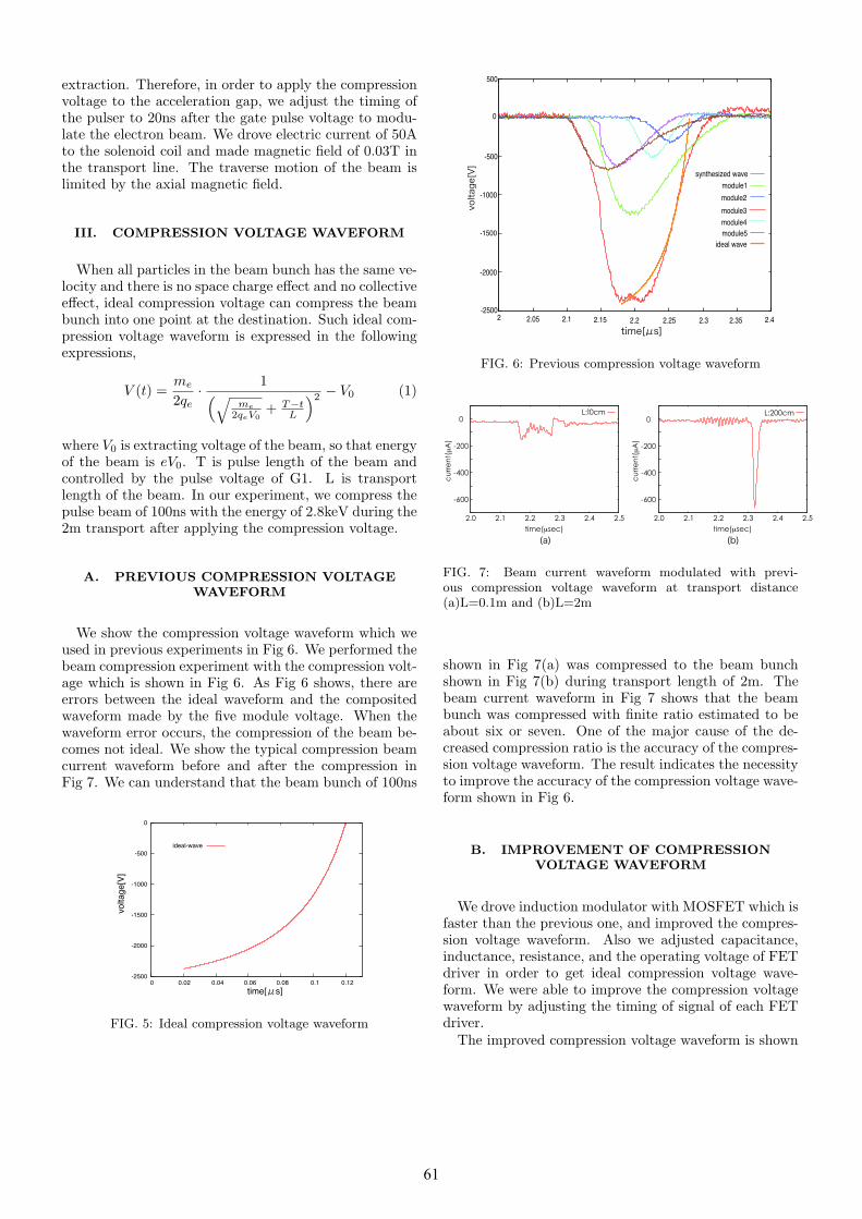
extraction. Therefore, in order to apply the compressionvoltage to the acceleration gap, we adjust the timing ofthe pulser to 20ns after the gate pulse voltage to modu-late the electron beam. We drove electric current of 50Ato the solenoid coil and made magnetic field of 0.03T inthe transport line. The traverse motion of the beam islimited by the axial magnetic field.
III. COMPRESSION VOLTAGE WAVEFORM
When all particles in the beam bunch has the same ve-locity and there is no space charge effect and no collectiveeffect, ideal compression voltage can compress the beambunch into one point at the destination. Such ideal com-pression voltage waveform is expressed in the followingexpressions,
V (t) =me
2qe· 1(√
me
2qeV0+ T−t
L
)2 − V0 (1)
where V0 is extracting voltage of the beam, so that energyof the beam is eV0. T is pulse length of the beam andcontrolled by the pulse voltage of G1. L is transportlength of the beam. In our experiment, we compress thepulse beam of 100ns with the energy of 2.8keV during the2m transport after applying the compression voltage.
A. PREVIOUS COMPRESSION VOLTAGEWAVEFORM
We show the compression voltage waveform which weused in previous experiments in Fig 6. We performed thebeam compression experiment with the compression volt-age which is shown in Fig 6. As Fig 6 shows, there areerrors between the ideal waveform and the compositedwaveform made by the five module voltage. When thewaveform error occurs, the compression of the beam be-comes not ideal. We show the typical compression beamcurrent waveform before and after the compression inFig 7. We can understand that the beam bunch of 100ns
-2500
-2000
-1500
-1000
-500
0
0 0.02 0.04 0.06 0.08 0.1 0.12
vo
lta
ge
[V]
time[μs]
ideal-wave
FIG. 5: Ideal compression voltage waveform
-500
-1000
-1500
-2000
-2500
500
time[μs]
0
ideal wave
voltage[V]
2 2.05 2.1 2.15 2.2 2.25 2.3 2.35 2.4
synthesized wave
module1
module5
module4
module3
module2
FIG. 6: Previous compression voltage waveform
0
cu
rre
nt(μ
A)
-200
-400
-600
time(μsec)
2.0 2.1 2.52.42.32.2
L :10cm0
cu
rre
nt(μ
A)
-200
-400
-600
time(μsec)
2.0 2.1 2.52.42.32.2
L:200cm
(a) (b)
FIG. 7: Beam current waveform modulated with previ-ous compression voltage waveform at transport distance(a)L=0.1m and (b)L=2m
shown in Fig 7(a) was compressed to the beam bunchshown in Fig 7(b) during transport length of 2m. Thebeam current waveform in Fig 7 shows that the beambunch was compressed with finite ratio estimated to beabout six or seven. One of the major cause of the de-creased compression ratio is the accuracy of the compres-sion voltage waveform. The result indicates the necessityto improve the accuracy of the compression voltage wave-form shown in Fig 6.
B. IMPROVEMENT OF COMPRESSIONVOLTAGE WAVEFORM
We drove induction modulator with MOSFET which isfaster than the previous one, and improved the compres-sion voltage waveform. Also we adjusted capacitance,inductance, resistance, and the operating voltage of FETdriver in order to get ideal compression voltage wave-form. We were able to improve the compression voltagewaveform by adjusting the timing of signal of each FETdriver.
The improved compression voltage waveform is shown
6161
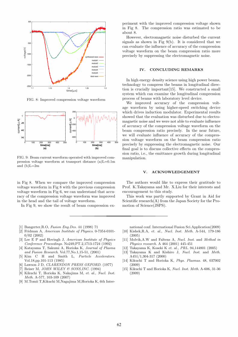
-2500
-2000
-1500
-1000
-500
0
500
1.1 1.15 1.2 1.25 1.3
module1
module2
module3
module4
module5
synthesized wave
ideal wave
time[μs]
voltage[V]
FIG. 8: Improved compression voltage waveform
-600
-400
-200
0
200
0 100 200 300 400 500
curr
ent[μ
A]
time[ns]
�
� � � �
� �
� � �
curr
ent[μ
A]
time[ns]
0 100 200 300 400 500
(a) (b)
FIG. 9: Beam current waveform operated with improved com-pression voltage waveform at transport distance (a)L=0.1mand (b)L=2m
in Fig 8. When we compare the improved compressionvoltage waveform in Fig 8 with the previous compressionvoltage waveform in Fig 6, we can understand that accu-racy of the compression voltage waveform was improvedin the head and the tail of voltage waveform.
In Fig 9, we show the result of beam compression ex-
periment with the improved compression voltage shownin Fig 8. The compression ratio was estimated to beabout 8.
However, electromagnetic noise disturbed the currentsignals as shown in Fig 9(b). It is considered that wecan evaluate the influence of accuracy of the compressionvoltage waveform on the beam compression ratio moreprecisely by suppressing the electromagnetic noise.
IV. CONCLUDING REMARKS
In high energy density science using high power beams,technology to compress the beams in longitudinal direc-tion is crucially important[15]. We constructed a smallsystem which can examine the longitudinal compressionprocess of beams with laboratory level device.
We improved accuracy of the compression volt-age waveform by using higher-speed switching devicewhich drives induction modulator. Experimental resultsshowed that the evaluation was disturbed due to electro-magnetic noise and we were not able to evaluate influenceof accuracy of the compression voltage waveform on thebeam compression ratio precisely. In the near future,we will evaluate influence of accuracy of the compres-sion voltage waveform on the beam compression ratioprecisely by suppressing the electromagnetic noise. Ourfinal goal is to discuss collective effects on the compres-sion ratio, i.e., the emittance growth during longitudinalmanipulation.
V. ACKNOWLEDGEMENT
The authors would like to express their gratitude toProf. K.Takayama and Mr. X.Liu for their interests andencouragement to this study.
This work was partly supported by Grant in Aid forScientific research(A) from the Japan Society for the Pro-motion of Science(JSPS).
[1] Bangerter,R.O, Fusion Eng.Des. 44 (1998) 71[2] Fridman A, American Institute of Physics. 0-7354-0101-
0/02 (2002)[3] Lee E P and Hovingh J, American Institute of Physics
Conference Proceedings. No249,PT.2,1713-1724 (1992)[4] Katayama T, Sakumi A, Horioka K, Journal of Plasma
and Fusion Research. Vol.77,No.1,15-51, (2001)[5] Kim C H and Smith L, Particle Accelerators.
Vol.18,pp.101-113 (1985)[6] Lawson J D, CLARENDON PRESS OXFORD. (1977)[7] Reiser M, JOHN WILEY & SONS,INC. (1994)[8] Kikuchi T, Horioka K, Nakajima M, et. al., Nucl. Inst.
Meth. A-577, 103-109 (2007)[9] M.Tomii T,Kikuchi M,Nagajima M,Horioka K, 6th Inter-
national conf. International Fusion Sci.Application(2009)[10] Kishek,R.A, et. al., Nucl. Inst. Meth. A-544, 179-186
(2005)[11] Molvik,A.W and Faltens A, Nucl. Inst. and Method in
Physics research. A 464 (2001) 445-451[12] Takayama K, Koseki K et. al., PRL. 94,144801 (2005)[13] Takayama K and Kishiro J, Nucl. Inst. and Meth.
A451/1,304-317 (2000)[14] Kikuchi T and Horioka K, Phys. Plasmas. 48, 037002
(2009)[15] Kikuchi T and Horioka K, Nucl. Inst. Meth. A-606, 31-36
(2009)
6262

Theoretical Study on Population Inversion of Hydrogen-like Nitrogen in Recombining Plasma
T. Ozawa, Y. Ishizuka, H. Kumai, E. Hotta, K. Horioka, and T. Kawamura
Tokyo Institute of Technology, Department of Energy Sciences,
Nagatsuta 4259, Midori, Yokohama, Kanagawa.
ABSTRACT Discharge produced plasma (DPP) is a promising tool to generate effective extreme ultraviolet (EUV) light. Hydrogen-like nitrogen ions are one of good candidates to get photons at about 13.4 nm with an optical allowed atomic transition from n=3 to 2, where n stands for a principal quantum number. To get an optimum condition for the generation of about 13.4 nm laser light, we focus on the properties of population inversion between n=3 and 2 in recombining phase. Population inversion is calculated in the framework of population kinetics and an inversion factor F is estimated. The higher plasma density is up to 1019 cc 1, the higher F can be obtained and the shorter becomes the duration of the population inversion. Finally, to get enough GL, where G is a gain for raising at about 13.4nm, and L is created plasma length (L is determined by the duration), the competition between the increase in F and the reduction of the duration at higher plasma density seems to be very critical.
Keywords
Discharge produced plasma, Population inversion, Extreme ultraviolet light, Hydrogen-like nitrogen
1. Introduction A short-wavelength light source has been used for such industrial applications as nanostructure imaging and creation [1]. Especially, extreme ultraviolet (EUV) light is one of the most promising candidates for the next generation lithography. The wavelength of EUV light is typically 5 ~ 40 nm, and can be obtained by creation of hot dense plasma. The EUV light generation has been experimentally done by intense laser light and high current discharge [2,3]. In general, hot dense plasma creation by discharge seems to be more efficient due to its compact and simple scheme compared with that by laser irradiation [4]. In this study, hydrogen-like nitrogen is focused as one of EUV light emitters of which wavelength is about 13.4 nm. The wavelength is near that for the next generation semiconductor lithography, and may be expected to have potential for the industrial use described above. The 13.4 nm light comes from an optical allowed transition from
n=3 to 2 (Balmer-�). To get enough intensity of the radiation, nitrogen must be ionized up to the ionization degree of six, and the associated atomic states are higher ones compared with the conventional hydrogen-like line emission, for example, Ly-� and Ly-� and so on. Therefore, a recombination scheme may work well. In the scheme, hot dense fully stripped nitrogen plasma is created and the hydrogen-like nitrogen is populated by collisional recombination with rapidly plasma expansion and cooling, resulting in the creation of population inversion and the lasing of Balmer-�. A research with a magnetohydrodynamic (MHD) and a plasma ion kinetics codes for Z-pinch recombination pumping was done [5]. However, in this study, because of plasma motion, understanding for the lasing characteristics in the viewpoint of atomic population kinetics is not clear. To gain insight into the efficient generation of the EUV laser light, population kinetics simulation with a stepwise
6363
cooling profile for the electron temperature is carried out. The ion density is kept constant since clear dependence on the plasma parameters may be obtained. In a sense, this cooling condition is expected to give us strong nonequilibrium properties on atomic processes, and a maximum inversion factor can be expected. Finally, we can gain an insight into the potential of the lasing of nitrogen at about 13.4 nm and an optimum condition to create a population inversion between n=3 and 2. 2. Estimation of lasing performance The laser intensity I is expressed by using the incident intensity I0,
I = I0eGL. (1) Here, L is plasma length, G is a gain coefficient, and the product GL is an index to show lasing performance [6]. With the cross-section of stimulated emission �stim, the gain coefficient of Balmer-� is
G = Nn=3�stimF, (2) where F stands for an inversion factor and can be written as follows.
F = 1 (Nn=2 /gn=2 )/(Nn=3 /gn=3) (3) Nn=2 and Nn=3 are the population density of n=2 and 3, respectively. gn=3 and gn=2 are the corresponding statistical weights. In this study, Nn=3F is focused to evaluate the gain, and normalized population inversion
, (4)
is defined. Here, � is the duration where population inversion between the target atomic levels is created. 3. Simulation conditions In plasma, atoms and ions undergo transitions between the quantum states through radiative and collisional processes [7].
Table 2.1 Plasma parameters. temperature [eV] ion density
ni [ cc�1] initial: TH final: TL 300 ~ 800 150 200 ~ 700 100 100 ~ 600 50
1016 ~ 1020
100 ~ 600 10
Fig. 2.1 Time evolution of electron temperature. Atomic processes are calculated with rapid plasma cooling. Here, the ion density is kept constant to exclude the effect of fluid motion in the calculation of population kinetics. Table 2.1 shows the plasma parameters which can be obtained in the plasma creation by discharge, and the plasma cooling is assumed to be a stepwise shown in fig. 2.1. 4. Simulation results and discussion Fig. 3.1 shows the population densities of hydrogen-like nitrogen ions per statistical weights (N/g). The initial electron temperature TH is assumed to be 300 eV, and the final one is 50 eV. The ion density is 1017~18 cc�1. In this case, the population inversion is created, and we can see that Nn=3/gn=3 is higher than Nn=2/gn=2. The higher the plasma ion density is, the higher is N/g and the shorter becomes the duration of the population inversion �. This is because a collision between an ion and an electron becomes frequent with increase in the ion density. The plasma length L can be approximately estimated by the product of � and the speed of light c. For example, when the initial and the final temperatures are 300 eV and 10 eV and the ion density is 1019 cc�1 (the corresponding result is not given in fig. 3.1.), L is on the order of about ten centimeters. L may be enough when the ion density is below 1019 cc�1. However, the population inversion quickly reduced and may become too small to amplify the EUV light with decrease in the ion density. The spontaneous emission from n=3 to 2 occurs about 10 ps after the population Nn=3 is created, which can be estimated by the Einstein’s transition probability. Hence, the duration of the population inversion must be greater than the time.
Nn=3Fdt0
�
� ni�
time0
TH
TL
elec
tron
tem
pera
ture
6464
Fig. 3.1 The population densities of hydrogen-like nitrogen ions per statistical weights (n stands for principal quantum number, (a) ni = 1017 cc�1 and (b) ni = 1018 cc�1).
Fig. 3.2 Normalized population inversion at (a) TL=150 eV, (b) TL=100 eV and (c) TL=50 eV. The dependence of the population inversion on the ion density and electron temperature is evaluated by eq. (4), and shown in fig. 3.2. When the final temperatures TL are 150 eV, 100 eV and 50 eV, the initial temperatures TH need respectively 500 eV, 300 eV and 200 eV to create the population inversion. The population inversion increases with increase in the initial temperature TH, and saturates at certain higher temperature. The reason is that nitrogen is fully stripped at such electron temperature. When the final temperature TL is higher than 100 eV, the initial temperature TH needs several hundreds electron volts or more, and when the final temperature TL is lower than 100 eV, the initial temperature TH is only about 200 ~ 300 eV.
1.2
1.0
0.8
0.6
0.4
0.2
0.0
11
0 100 200 300 400time [ns]
T = 50 eVL
T = 300 eVH
n = 10 cci17
(a)
–1
nn
n = 2n = 3
N /g
×10 [cc ]
–1
1.2
1.0
0.8
0.6
0.4
0.2
0.0
N /g
×10 [cc ]
13
time [ns]
T = 50 eVL
T = 300 eVH
n = 10 cci18
(b)
–1
nn
n = 2n = 3
–1
0 10 20 30 40
norm
aliz
ed p
opul
atio
n in
vers
ion
(a) T =150 eVL
T [eV]H
n =10 cc18 ‒1i
n =10 cc17 ‒1i
n =10 cc16 ‒1i
norm
aliz
ed p
opul
atio
n in
vers
ion
(c)
T = 50 eVL
T [eV]H
n =10 cc18 ‒1i
n =10 cc17 ‒1i
n =10 cc16 ‒1i
n =10 cc19 ‒1i
norm
aliz
ed p
opul
atio
n in
vers
ion
(b) T =100 eVL
T [eV]H
n =10 cc18 ‒1i
n =10 cc17 ‒1i
n =10 cc16 ‒1i
6565
The higher the ion density is, the higher is the population inversion. However, when the ion density is 1019 cc�1, population inversion is not created at the final temperatures TL of higher than 100 eV. Fig. 3.3 Normalized population inversion at ni=1018 cc�1. Fig. 3.3 shows that the population inversion at the ion density of 1018 cc�1. It indicates that the maximum of the population inversion is almost determined by the ion density, not by the final temperature TL. 5. Conclusions In this study, to get an optimum condition for the generation of about 13.4 nm laser light, we focus on the properties of the population inversion between n=3 and 2 (Balmer-�) in recombining phase. In the estimation of the inversion factor F, it is found that higher F can be obtained at higher plasma density. However, the duration of the population inversion � becomes shorter with increase in the plasma density. Since the duration may become too short to get enough GL, the plasma density cannot be high. Numerical simulation of the population inversion with a stepwise cooling shows that the difference of the electron temperatures between TH and TL is about a few hundreds electron volts at TL�100 eV. The maximum of the population inversion is almost determined by the ion density, and has a weak
dependence on TL. In the future, since we focus Nn=3F, the gain coefficient must be estimated. In the estimation, the spectral broadening is essential, and the Stark broadening may play an important role to determine the coefficient. We will report the results somewhere. References [1] D. T. Attwood, “Soft X-rays and extreme
ultraviolet radiation”, Cambridge University Press (1990).
[2] D. L. Matthews et al., Phys. Rev. Lett., “Demonstration of a Soft X-Ray Amplifier” 54, pp.110-113 (1985).
[3] M. C. Marconi and J. J. Rocca, “Time-resolved extreme ultraviolet emission from a highly ionized lithium capillary discharge”, Appl. Phys. Lett., 54, pp.2180-2182 (1989).
[4] J. J. Rocca et al., “Demonstration of a Discharge Pumped Table-Top Soft-X-Ray Laser”, Phys. Rev. Lett., 73, pp.2192-2195 (1994).
[5] P. Vrba, et al., “Modeling of capillary Z-pinch recombination pumping of boron extreme ultraviolet laser”, Phys. Plasmas, 16, 073105 (2009).
[6] R. C. Elton, “X-ray lasers”, Academic Press, Inc. (1990).
[7] T. Fujimoto, “Plasma Spectroscopy”, Clarendon Press (2004).
norm
aliz
ed p
opul
atio
n in
vers
ion
T =150 eVL
T [eV]H
n =10 cc18 ‒1i
T =100 eVL
T = 50 eVL
6666
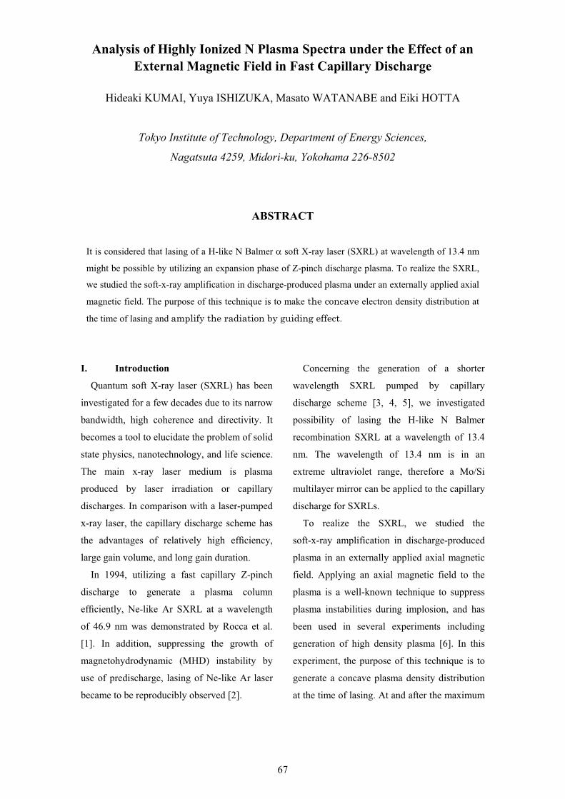
Analysis of Highly Ionized N Plasma Spectra under the Effect of an External Magnetic Field in Fast Capillary Discharge
Hideaki KUMAI, Yuya ISHIZUKA, Masato WATANABE and Eiki HOTTA
Tokyo Institute of Technology, Department of Energy Sciences,
Nagatsuta 4259, Midori-ku, Yokohama 226-8502
ABSTRACT
It is considered that lasing of a H-like N Balmer � soft X-ray laser (SXRL) at wavelength of 13.4 nm
might be possible by utilizing an expansion phase of Z-pinch discharge plasma. To realize the SXRL,
we studied the soft-x-ray amplification in discharge-produced plasma under an externally applied axial
magnetic field. The purpose of this technique is to make the concave electron density distribution at
the time of lasing and amplify the radiation by guiding effect.
I. Introduction
Quantum soft X-ray laser (SXRL) has been
investigated for a few decades due to its narrow
bandwidth, high coherence and directivity. It
becomes a tool to elucidate the problem of solid
state physics, nanotechnology, and life science.
The main x-ray laser medium is plasma
produced by laser irradiation or capillary
discharges. In comparison with a laser-pumped
x-ray laser, the capillary discharge scheme has
the advantages of relatively high ef�ciency,
large gain volume, and long gain duration.
In 1994, utilizing a fast capillary Z-pinch
discharge to generate a plasma column
ef�ciently, Ne-like Ar SXRL at a wavelength
of 46.9 nm was demonstrated by Rocca et al.
[1]. In addition, suppressing the growth of
magnetohydrodynamic (MHD) instability by
use of predischarge, lasing of Ne-like Ar laser
became to be reproducibly observed [2].
Concerning the generation of a shorter
wavelength SXRL pumped by capillary
discharge scheme [3, 4, 5], we investigated
possibility of lasing the H-like N Balmer
recombination SXRL at a wavelength of 13.4
nm. The wavelength of 13.4 nm is in an
extreme ultraviolet range, therefore a Mo/Si
multilayer mirror can be applied to the capillary
discharge for SXRLs.
To realize the SXRL, we studied the
soft-x-ray amplification in discharge-produced
plasma in an externally applied axial magnetic
field. Applying an axial magnetic field to the
plasma is a well-known technique to suppress
plasma instabilities during implosion, and has
been used in several experiments including
generation of high density plasma [6]. In this
experiment, the purpose of this technique is to
generate a concave plasma density distribution
at the time of lasing. At and after the maximum
6767
pinch, a convex electron density distribution
will be formed in usual Z-pinch plasma. This
electron density distribution refracts the ray of
light off the axis, as shown in Fig.1. Refraction
decreases the effective gain coefficient and
limits the maximum gain-length product that
could be obtained. For this reason, we aimed to
make the concave electron density distribution
at the time of lasing by applying axial magnetic
field and amplify the radiation by guiding
effect. In this paper we discuss the results of the
study of soft x-ray amplification in a
discharge-produced plasma column under the
influence of an axial magnetic field.
II. Experimental setup
Capillary discharge plasma was generated by
utilizing a triangular current with peak
amplitude of about 50 kA and a pulse width of
about 50 ns. A pulsed power supply system
with a pulse shaping transmission line as shown
in Fig. 2 was used [7, 8]. An alumina (Al2O3)
ceramics capillary with an inner radius of 1.5
mm and a length of 150 mm was filled with
initial nitrogen molecular gas at pressure of
about 600 mTorr.
The gas was pre-ionized by RC discharge
with amplitude of about 10 A and a decay time
constant of 3 �s. Schematic diagram of time
integrated spectrum pinhole imaging set-up is
illustrated in Fig. 3. The measurement of
radiation from the nitrogen plasma was carried
out using a transmission grating spectrometer
with a lattice constant of 1/1000 mm-1 in
combination with an X-ray CCD camera which
has 1024 1024 pixels. Each pixel has an area
of 13-�m square. The transmission grating was
placed at a distance of 600 mm from the end of
capillary and a distance between the grating
and the CCD camera was 425 mm. In addition,
two slits of 1 mm 5 mm were placed between
the capillary and the transmission grating, and
the diameter of the transmission grating was 50
�m.
The axial magnetic field was generated by
using a 4-cm diameter, 15-cm long coil
positioned concentrically with the capillary
channel. The coil, which was excited by a DC power supply, produced magnetic fields up to
15 mT.
Fig. 2. Experimental setup for lasing H-like N
soft X-ray laser
Fig. 3. Time integrated spectrum pinhole
imaging set-up
Fig.1. Refraction effect of electron density
gradient
6868
When an axial magnetic field is applied to
plasma, the magnetic flux is conserved in the
plasma because of induced azimuthal current in
plasma shell. The magnetic flux is collected by
the imploding plasma, which leads to increase
of the magnetic field strength inside the plasma.
When the plasma is compressed to a radius of r,
the magnetic flux density inside plasma, B, is
given by
� � ������
� (1)
where �� �� ���� are the initial magnetic
flux density of the external field, initial plasma
radius, and leakage of the magnetic flux during
implosion.
From previous experimental results, the
plasma is compressed to one tenth of initial
plasma radius at maximum pinch. Therefore,
the multiplication factor of 100 in the magnetic
flux density is expected.
III. Experimental results and discussions
The effects of the axial magnetic field [9, 10]
on the time-resolved XRD signals radiated
from fast capillary Z-pinch discharge plasma
are illustrated in Fig. 4. Axial magnetic field
inside the plasma opposes the compression
force driven by the plasma current. This
phenomenon prevents the plasma compression
and the increase of the electron temperature and
density, which may lead to the decrease of
radiation intensity. However no change is
observed in radiation intensity with an axial
magnetic field. This result indicates that an
externally applied axial magnetic �eld of 15
mT does not signi�cantly affect the evolution
of the plasma. The cause may be the negligibly
small compressed axial magnetic �eld strength
��� ��� � ����� compared with the
self-generated azimuthal magnetic �eld
��� � �� ���� = 33 T.
Fig. 4. XRD signals radiated from fast capillary
Z-pinch discharge plasma. (a) Without external
magnetic field. (b) With axial magnetic field of
15 mT.
Fig. 5. Emission spectrum profiles without and
with axial magnetic field of 15 mT
6969
Fig. 6. Soft-x-ray pro�les (a) 9 nm, (b) 13.4 nm, (c) 18 nm and (d) 27 nm corresponding to
discharges of approximately 45 kA through 15-cm-long, 3-mm-diameter capillary without and with
axial magnetic �eld of 0.15 T
The effects of the axial magnetic �eld on the
intensity pro�le of the emission spectrum at
wavelength of below 27 nm are illustrated in
Fig. 5. As shown in Fig.5, the intensities of
spectrum line at wavelengths below 6 nm and
over 21 nm slightly increase by an axial
magnetic field. However, intensity of spectrum
line at wavelengths over 20 nm decreases.
Figure 6 shows radiation patterns recorded
along the direction of the spectrometer slit
under the condition of no external magnetic
�eld applied.
(a) �=9 nm
This line corresponds to spectrum of highly
ionized NVII state. The beam pro�le exhibits a
double peak. Since electron temperature of Te
�150 eV is needed in order to generate NVII
ions, NVII state is considered to be obtained
after maximum pinch. Therefore, this line may
be affected by convex electron density
distribution. The intensity of radiation in axis
region obtained without axial magnetic field is
lower than that with magnetic field. This result
suggests that the ray of radiation is bended off
the axial region by convex electron density
distribution. With magnetic field, the radiation
patterns sharpen and the intensity of radiation
increases, suggesting the waveguide effect.
7070
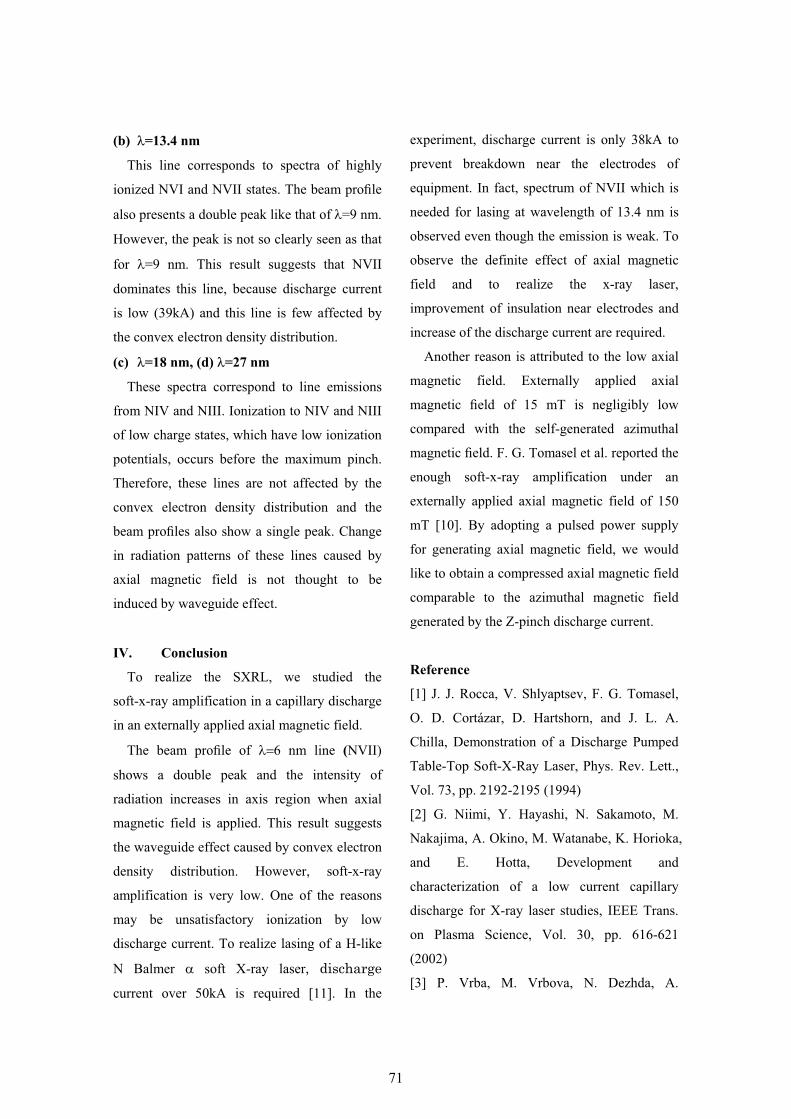
(b) �=13.4 nm
This line corresponds to spectra of highly
ionized NVI and NVII states. The beam pro�le
also presents a double peak like that of �=9 nm.
However, the peak is not so clearly seen as that
for �=9 nm. This result suggests that NVII
dominates this line, because discharge current
is low (39kA) and this line is few affected by
the convex electron density distribution.
(c) �=18 nm, (d) �=27 nm
These spectra correspond to line emissions
from NIV and NIII. Ionization to NIV and NIII
of low charge states, which have low ionization
potentials, occurs before the maximum pinch.
Therefore, these lines are not affected by the
convex electron density distribution and the
beam pro�les also show a single peak. Change
in radiation patterns of these lines caused by
axial magnetic field is not thought to be
induced by waveguide effect.
IV. Conclusion
To realize the SXRL, we studied the
soft-x-ray amplification in a capillary discharge
in an externally applied axial magnetic field.
The beam pro�le of ��6 nm line (NVII)
shows a double peak and the intensity of
radiation increases in axis region when axial
magnetic field is applied. This result suggests
the waveguide effect caused by convex electron
density distribution. However, soft-x-ray
amplification is very low. One of the reasons
may be unsatisfactory ionization by low
discharge current. To realize lasing of a H-like
N Balmer � soft X-ray laser, discharge current over 50kA is required [11]. In the
experiment, discharge current is only 38kA to
prevent breakdown near the electrodes of
equipment. In fact, spectrum of NVII which is
needed for lasing at wavelength of 13.4 nm is
observed even though the emission is weak. To
observe the definite effect of axial magnetic
field and to realize the x-ray laser,
improvement of insulation near electrodes and
increase of the discharge current are required.
Another reason is attributed to the low axial
magnetic field. Externally applied axial
magnetic �eld of 15 mT is negligibly low
compared with the self-generated azimuthal
magnetic �eld. F. G. Tomasel et al. reported the
enough soft-x-ray amplification under an
externally applied axial magnetic field of 150
mT [10]. By adopting a pulsed power supply
for generating axial magnetic field, we would
like to obtain a compressed axial magnetic field
comparable to the azimuthal magnetic field
generated by the Z-pinch discharge current.
Reference
[1] J. J. Rocca, V. Shlyaptsev, F. G. Tomasel,
O. D. Cortázar, D. Hartshorn, and J. L. A.
Chilla, Demonstration of a Discharge Pumped
Table-Top Soft-X-Ray Laser, Phys. Rev. Lett.,
Vol. 73, pp. 2192-2195 (1994)
[2] G. Niimi, Y. Hayashi, N. Sakamoto, M.
Nakajima, A. Okino, M. Watanabe, K. Horioka,
and E. Hotta, Development and
characterization of a low current capillary
discharge for X-ray laser studies, IEEE Trans.
on Plasma Science, Vol. 30, pp. 616-621
(2002)
[3] P. Vrba, M. Vrbova, N. Dezhda, A.
7171
Bobrova, and P. V. Sasorov, Modeling of a
nitrogen x-ray laser pumped by capillary
discharge, Central European Journal of Physics,
Vol. 3, pp. 564-580 (2005)
[4] N. S. Kampel, A. Rikanati, I. Be'ery, A.
Ben-Kish, A. Fisher, and A. Ron, Feasibility of
a nitrogen-recombination soft-x-ray laser using
capillary discharge Z pinch, Phys. Rev. E, Vol.
78, 056404 (2008)
[5] Y. Sakai, S. Takahashi, T. Hosokai, M.
Watanabe, A. Okino and E. Hotta, The
possibility of a capillary discharge soft X-ray
laser with shorter wavelength by utilizing a
recombination scheme, Journal of Plasma and
Fusion Research Series, Vol. 8, pp. 1317-1312
(2009)
[6] Liberman M A, De Groot J S, Toor A and
Spielman R B, Physics of High-density Z-pinch
Plasmas, New York, Springer, 1999
[7] Y. Sakai, T. Komatsu, I. Song, M.
Watanabe, G. H Kim and E. Hotta, High
efficient pulsed power supply system with a
two-stage LC generator and a step-up
transformer for fast capillary discharge soft
X-ray laser at shorter wavelength, Review of
Scientific Instruments., Vol. 81, 013303 (2010)
[8] Y. Sakai, S. Takahashi, M. Watanabe, G. H.
Kim and E. Hotta, Pulsed current wave shaping
with a transmission line by utilizing
superposition of a forward and a backward
voltage wave for fast capillary Z-pinch
discharge, Review of Scientific Instruments,
Vol. 81, 043504 (2010)
[9] R. A. London, Beam optics of exploding
foil plasma x-ray lasers, Phys. Fluids, Vol. 31,
p.184 (1988)
[10] F. G. Tomasel, V. N. Shlyaptsev, and J. J.
Rocca, Enhanced beam characteristics of a
discharge-pumped soft x-ray amplifier by an
axial magnetic field, Phys. Rev. A, Vol. 54, No.
3, pp.2474-2478 (1996)
[11] : Z
(2010)
7272
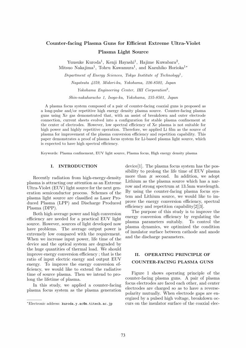
Counter-facing Plasma Guns for Efficient Extreme Ultra-Violet
Plasma Light Source
Yuusuke Kuroda1, Kenji Hayashi1, Hajime Kuwabara2,Mitsuo Nakajima1, Tohru Kawamura1, and Kazuhiko Horioka1∗
Department of Energy Sciences, Tokyo Institute of Technology1,
Nagatsuta 4259, Midori-ku, Yokohama, 226-8502, Japan
Yokohama Engineering Center, IHI Corporation2,
Shin-nakaharacho 1, Isogo-ku, Yokohama, 235-8501, Japan
A plasma focus system composed of a pair of counter-facing coaxial guns is proposed asa long-pulse and/or repetitive high energy density plasma source. Counter-facing plasmaguns using Xe gas demonstrated that, with an assist of breakdown and outer electrodeconnection, current sheets evolved into a configuration for stable plasma confinement atthe center of electrodes. However, low spectral efficiency of Xe plasma is not suitable forhigh power and highly repetitive operation. Therefore, we applied Li film as the source ofplasma for improvement of the plasma conversion efficiency and repetition capability. Thispaper demonstrates a proof of plasma focus system for Li-based plasma light source, whichis expected to have high spectral efficiency.
Keywords: Plasma confinement, EUV light source, Plasma focus, High energy density plasma
I. INTRODUCTION
Recently radiation from high-energy-densityplasma is attracting our attention as an ExtremeUltra-Violet (EUV) light source for the next gen-eration semiconductor process. Schemes of theplasma light source are classified as Laser Pro-duced Plasma (LPP) and Discharge ProducedPlasma (DPP).
Both high average power and high conversionefficiency are needed for a practical EUV lightsource. However, sources of light developed nowhave problems. The average output power isextremely low compared with the requirement.When we increase input power, life time of thedevice and the optical system are degraded bythe huge quantities of thermal load. We shouldimprove energy conversion efficiency ; that is theratio of input electric energy and output EUVenergy. To improve the energy conversion ef-ficiency, we would like to extend the radiativetime of source plasma. Then we intend to pro-long the lifetime of plasma.
In this study, we applied a counter-facingplasma focus system as the plasma generation
∗Electronic address: [email protected]
device[1]. The plasma focus system has the pos-sibility to prolong the life time of EUV plasmamore than μ second. In addition, we adoptLithium as the plasma source which has a nar-row and strong spectrum at 13.5nm wavelength.By using the counter-facing plasma focus sys-tem and Lithium source, we would like to im-prove the energy conversion efficiency, spectralefficiency and repetition capability[2][3].
The purpose of this study is to improve theenergy conversion efficiency by regulating theplasma parameters suitably. To control theplasma dynamics, we optimized the conditionof insulator surface between cathode and anodeand the discharge parameters.
II. OPERATING PRINCIPLE OF
COUNTER-FACING PLASMA GUNS
Figure 1 shows operating principle of thecounter-facing plasma guns. A pair of plasmafocus electrodes are faced each other, and centerelectrodes are charged so as to have a reverse-polarity mutually. When electrode gaps are en-ergized by a pulsed high voltage, breakdown oc-curs on the insulator surface of the coaxial elec-
7373
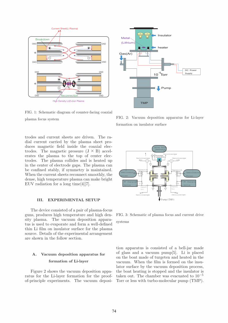
+
GND
GND
GND
GND Reconnection
+
GND
GND
GND
GND
Breakdown
B
Current Sheet(Li Plasma)
High Density Li(2+)ion Plasma
FIG. 1: Schematic diagram of counter-facing coaxial
plasma focus system
trodes and current sheets are driven. The ra-dial current carried by the plasma sheet pro-duces magnetic field inside the coaxial elec-trodes. The magnetic pressure (J × B) accel-erates the plasma to the top of center elec-trodes. The plasma collides and is heated upin the center of electrode gaps. The plasma canbe confined stably, if symmetry is maintained.When the current sheets reconnect smoothly, thedense, high temperature plasma can make brightEUV radiation for a long time[4][7].
III. EXPERIMENTAL SETUP
The device consisted of a pair of plasma-focusguns, produces high temperature and high den-sity plasma. The vacuum deposition appara-tus is used to evaporate and form a well-definedthin Li film on insulator surface for the plasmasource. Details of the experimental arrangementare shown in the follow section.
A. Vacuum deposition apparatus for
formation of Li-layer
Figure 2 shows the vacuum deposition appa-ratus for the Li-layer formation for the proof-of-principle experiments. The vacuum deposi-
10 Torr-5
Pump
Gas(Ar)
Insulator
heater
DC Power
Supply
Metal
(Lithium)
TMP
FIG. 2: Vacuum deposition apparatus for Li-layer
formation on insulator surface
Pump(TMP)
Oscilloscope Oscilloscope
OscilloscopeOscilloscope
C C
Gapswitch Gapswitch
Delay PulseGenerator
HV Charging
Device
Semiconductor
Pulser
HV Charging
Device
V V
Semiconductor
Pulser
Rogowski
Coil
Rogowski
Coil
OscilloscopePhotodiode(AXUV 20HS1)
FIG. 3: Schematic of plasma focus and current drive
systems
tion apparatus is consisted of a bell-jar madeof glass and a vacuum pump[5]. Li is placedon the boat made of turgeten and heated in thevacuum. When the film is formed on the insu-lator surface by the vacuum deposition process,the boat heating is stopped and the insulator istaken out. The chamber was evacuated to 10−5
Torr or less with turbo-molecular pump (TMP).
7474
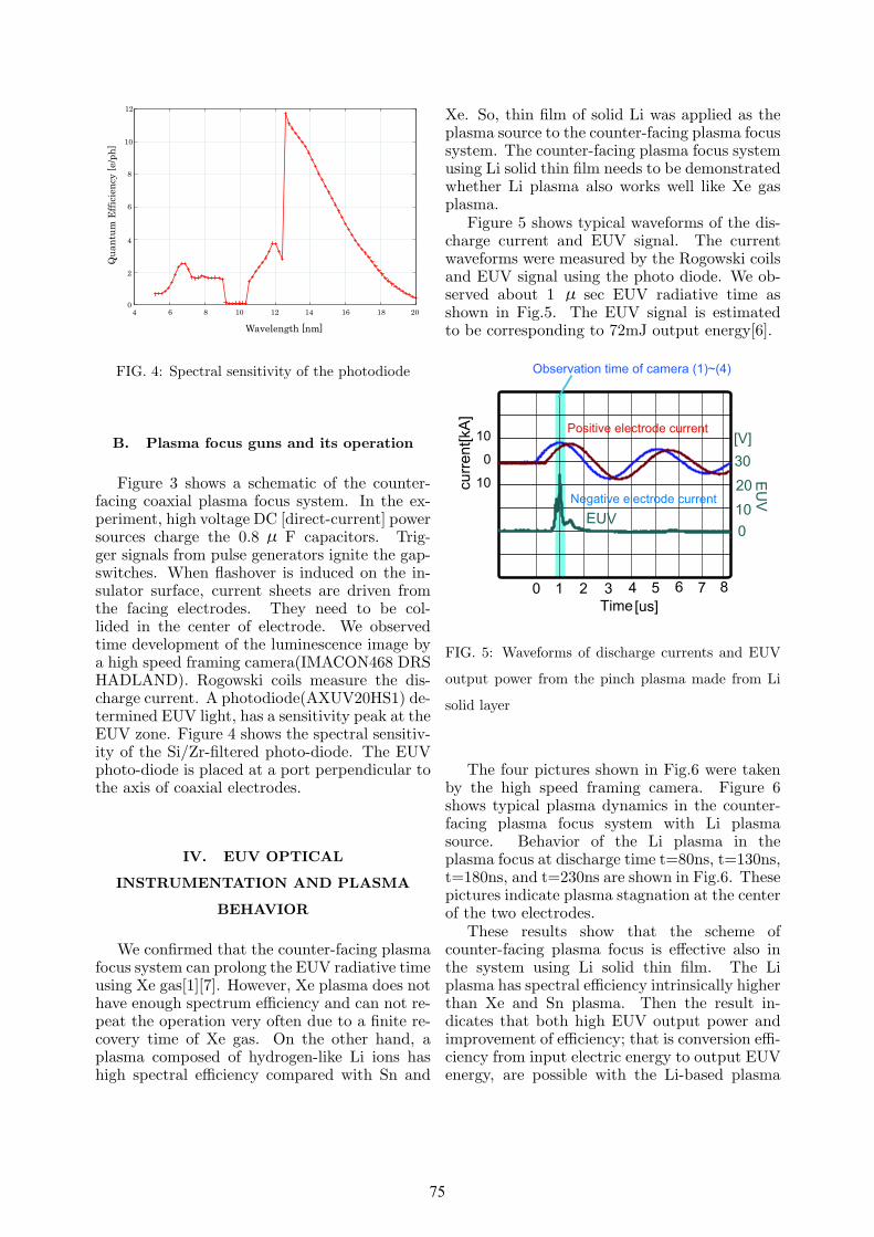
0
2
4
6
8
10
12
4 6 8 10 12
Wavelength [nm]
Qu
an
tum
Eff
icie
ncy
[e/
ph
]
14 16 18 20
FIG. 4: Spectral sensitivity of the photodiode
B. Plasma focus guns and its operation
Figure 3 shows a schematic of the counter-facing coaxial plasma focus system. In the ex-periment, high voltage DC [direct-current] powersources charge the 0.8 μ F capacitors. Trig-ger signals from pulse generators ignite the gap-switches. When flashover is induced on the in-sulator surface, current sheets are driven fromthe facing electrodes. They need to be col-lided in the center of electrode. We observedtime development of the luminescence image bya high speed framing camera(IMACON468 DRSHADLAND). Rogowski coils measure the dis-charge current. A photodiode(AXUV20HS1) de-termined EUV light, has a sensitivity peak at theEUV zone. Figure 4 shows the spectral sensitiv-ity of the Si/Zr-filtered photo-diode. The EUVphoto-diode is placed at a port perpendicular tothe axis of coaxial electrodes.
IV. EUV OPTICAL
INSTRUMENTATION AND PLASMA
BEHAVIOR
We confirmed that the counter-facing plasmafocus system can prolong the EUV radiative timeusing Xe gas[1][7]. However, Xe plasma does nothave enough spectrum efficiency and can not re-peat the operation very often due to a finite re-covery time of Xe gas. On the other hand, aplasma composed of hydrogen-like Li ions hashigh spectral efficiency compared with Sn and
Xe. So, thin film of solid Li was applied as theplasma source to the counter-facing plasma focussystem. The counter-facing plasma focus systemusing Li solid thin film needs to be demonstratedwhether Li plasma also works well like Xe gasplasma.
Figure 5 shows typical waveforms of the dis-charge current and EUV signal. The currentwaveforms were measured by the Rogowski coilsand EUV signal using the photo diode. We ob-served about 1 μ sec EUV radiative time asshown in Fig.5. The EUV signal is estimatedto be corresponding to 72mJ output energy[6].
[us]
[V]
EU
V
0
10
20
30
0 1 2 3 4 5 6 7 8
Time
EUV
Positive electrode current
Negative electrode current
Observation time of camera (1)~(4)
10
0
10curr
ent[kA
]
FIG. 5: Waveforms of discharge currents and EUV
output power from the pinch plasma made from Li
solid layer
The four pictures shown in Fig.6 were takenby the high speed framing camera. Figure 6shows typical plasma dynamics in the counter-facing plasma focus system with Li plasmasource. Behavior of the Li plasma in theplasma focus at discharge time t=80ns, t=130ns,t=180ns, and t=230ns are shown in Fig.6. Thesepictures indicate plasma stagnation at the centerof the two electrodes.
These results show that the scheme ofcounter-facing plasma focus is effective also inthe system using Li solid thin film. The Liplasma has spectral efficiency intrinsically higherthan Xe and Sn plasma. Then the result in-dicates that both high EUV output power andimprovement of efficiency; that is conversion effi-ciency from input electric energy to output EUVenergy, are possible with the Li-based plasma
7575
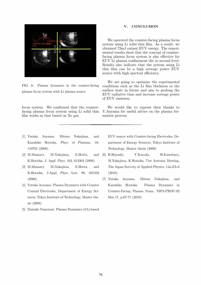
� �� �
FIG. 6: Plasma dynamics in the counter-facing
plasma focus system with Li plasma source
focus system. We confirmed that the counter-facing plasma focus system using Li solid thinfilm works as that based on Xe gas.
V. CONCLUSION
We operated the counter-facing plasma focussystem using Li solid thin film. As a result, weobtained 72mJ output EUV energy. The experi-mental results show that the concept of counter-facing plasma focus system is also effective forEUV Li plasma confinement theμ-second level.Results also indicate that the system using Lithin film can be a high average power EUVsource with high spectral efficiency.
We are going to optimize the experimentalconditions such as the Li film thickness or thesurface state in future and aim to prolong theEUV radiative time and increase average powerof EUV emission.
We would like to express their thanks toY.Aoyama for useful advice on the plasma for-mation process.
[1] Yutaka Aoyama, Mitsuo Nakajima, and
Kazuhiko Horioka, Phys. of Plasmas, 16,
110701 (2009).
[2] M.Masnavi, M.Nakajima, E.Hotta, and
K.Horioka, J. Appl. Phys. 103, 013303 (2008).
[3] M.Masnavi, M.Nakajima, E.Hotta, and
K.Horioka, J.Appl. Phys. Lett. 89, 031503
(2006).
[4] Yutaka Aoyama: Plasma Dynamics with Counter
Coaxial Electrodes, Department of Energy Sci-
ences, Tokyo Institute of Technology, Master the-
sis (2008)
[5] Daisuke Nunotani: Plasma Dynamics of Li-based
EUV source with Counter-facing Electrodes, De-
partment of Energy Sciences, Tokyo Institute of
Technology, Master thesis (2009)
[6] H.Hayashi, Y.Kuroda, H.Kuwabara,
M.Nakajima, K.Horioka, 71st Autumn Meeting,
The Japan Soci-ety of Applied Physics, 14a-ZA-6
(2010).
[7] Yutaka Aoyama, Mitsuo Nakajima, and
Kazuhiko Horioka: Plasma Dynamics in
Counter-Facing Plasma Guns, NIFS-PROC-82
Mar.17, p.67-71 (2010)
7676
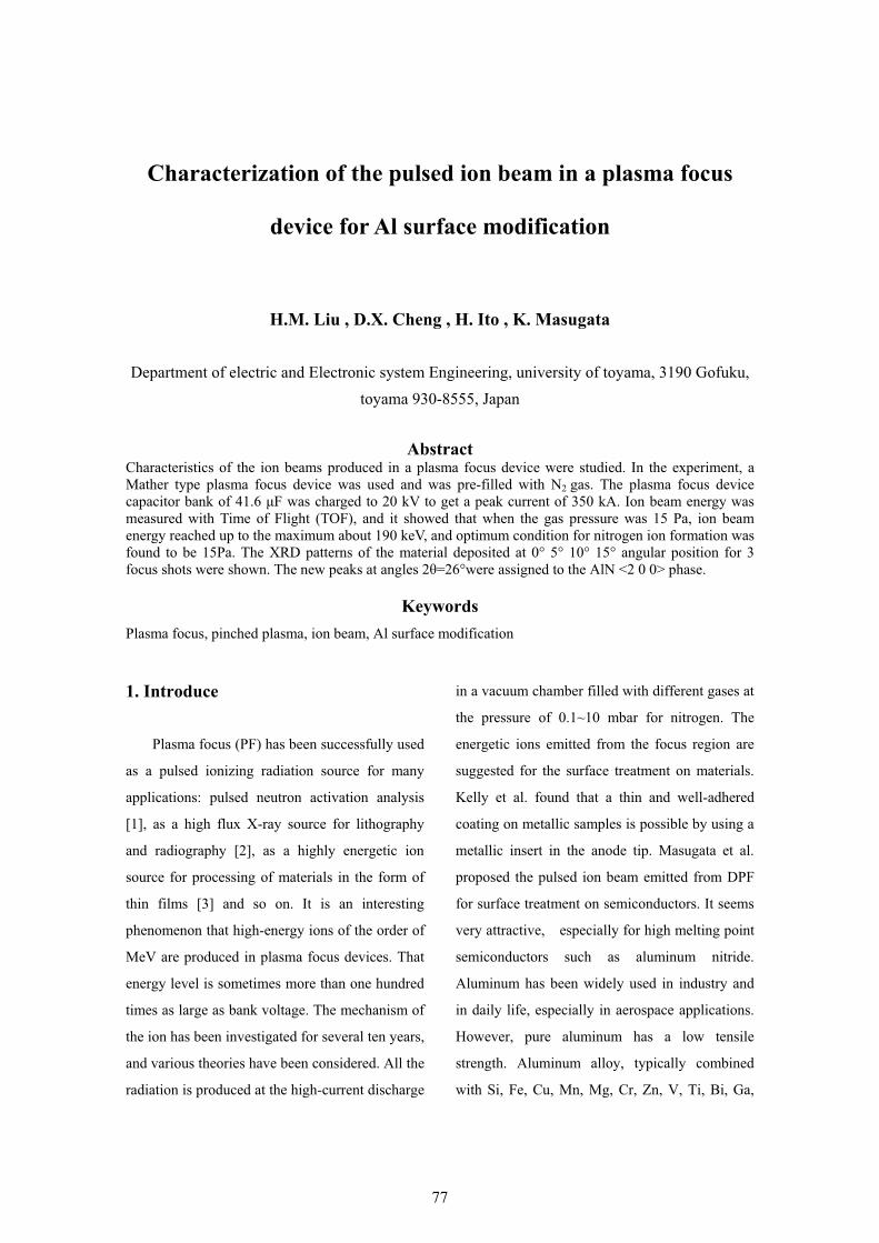
Characterization of the pulsed ion beam in a plasma focus
device for Al surface modification
H.M. Liu , D.X. Cheng , H. Ito , K. Masugata
Department of electric and Electronic system Engineering, university of toyama, 3190 Gofuku, toyama 930-8555, Japan
Abstract
Characteristics of the ion beams produced in a plasma focus device were studied. In the experiment, a Mather type plasma focus device was used and was pre-filled with N2 gas. The plasma focus device capacitor bank of 41.6 �F was charged to 20 kV to get a peak current of 350 kA. Ion beam energy was measured with Time of Flight (TOF), and it showed that when the gas pressure was 15 Pa, ion beam energy reached up to the maximum about 190 keV, and optimum condition for nitrogen ion formation was found to be 15Pa. The XRD patterns of the material deposited at 0° 5° 10° 15° angular position for 3 focus shots were shown. The new peaks at angles 2�=26°were assigned to the AlN <2 0 0> phase.
Keywords Plasma focus, pinched plasma, ion beam, Al surface modification
1. Introduce
Plasma focus (PF) has been successfully used
as a pulsed ionizing radiation source for many
applications: pulsed neutron activation analysis
[1], as a high flux X-ray source for lithography
and radiography [2], as a highly energetic ion
source for processing of materials in the form of
thin films [3] and so on. It is an interesting
phenomenon that high-energy ions of the order of
MeV are produced in plasma focus devices. That
energy level is sometimes more than one hundred
times as large as bank voltage. The mechanism of
the ion has been investigated for several ten years,
and various theories have been considered. All the
radiation is produced at the high-current discharge
in a vacuum chamber filled with different gases at
the pressure of 0.1~10 mbar for nitrogen. The
energetic ions emitted from the focus region are
suggested for the surface treatment on materials.
Kelly et al. found that a thin and well-adhered
coating on metallic samples is possible by using a
metallic insert in the anode tip. Masugata et al.
proposed the pulsed ion beam emitted from DPF
for surface treatment on semiconductors. It seems
very attractive, especially for high melting point
semiconductors such as aluminum nitride.
Aluminum has been widely used in industry and
in daily life, especially in aerospace applications.
However, pure aluminum has a low tensile
strength. Aluminum alloy, typically combined
with Si, Fe, Cu, Mn, Mg, Cr, Zn, V, Ti, Bi, Ga,
7777
Pb, Zr. AlN is a hard material with 11.8Gpa in
Knoop hardness. AlN is the only stable compound
in the binary system Al - N and exists in one
crystal structure. Pure AlN has a density of 3.26
g/cm3 and dissociates under atmospheric
pressure above 2500 °C. Pure AlN is colorless
and translucent but is easily colored by impurities.
Thus, carbon impurities cause the typical light
gray color of AlN powder. AlN powder is
susceptible to hydrolysis by water and humidity.
This is the reason for its characteristic ammonia
smell. Because AlN is a covalent compound,
limited atomic mobility prevents complete
densification of pure AlN. Thus, relatively high
pressures or sintering aids are required to assist
densification. Typical sintering additives are
rare-earth or alkaline-earth oxides. To achieve
high thermal conductivities mostly yttrium
compounds are used. The formation and micro
structural distribution of yttrium Al’s garnet
controls both densification and thermal properties.
2. Experiment set up What we used was mather type plasma focus
device [4]. Mather type plasma focus device is a
simple pulsed coaxial plasma accelerator that
produces a short but finite two dimensional non
cylindrical Z-pinch, at the end of the central
electrode, and compresses the plasma to very high
densities and temperatures of the order of 1-2KeV.
Plasma focus also serves as a source of high
energy density ion with energies from few keV to
hundreds of keV, X-rays, neutrons and relativistic
electrons. The plasma focus possesses the
advantages of small size, easy maintenance, and
technical simplicity of construction as well as
operation and considerably lower cost over
continuous accelerators. Electron and ion beams
emitted by PF devices have unique features for
each device. The device accelerates the ions to
high energy values by means of fast electric
discharge of only tens of kilovolts. The energy
profile of these ion beams is continuous from a
few tens keV to some hundreds keV. The ions
coming from the focus region are much more
energetic than those present in other material
processing reactors. These ions cause the heating
of the substrate during a deposition process which
eliminates the requirement of separate heating.
Another distinct advantage of this technique is
that the substrate needs not to be electrically
conductive. Thus many of the insulators and
semiconductors can be used for surface
modification. This technique, when used for
material processing purposes, especially in thin
film deposition gives the advantages of labor
savings, less treatment time, significant reduction
in energy consumption and high deposition rates.
Plasma focus device is made up of electrodes
and capacitor banks. Electrodes play the main role
in the formation of plasma inside the chamber,
where working gas is present. It provides the
positive and negative polarity to ionize the gas
atoms. The electrode arrangement of Mather type
plasma focus is shown in Fig1. It consist a central
rod which serves as the anode surrounded by 24
coaxial copper rods acting as the cathode. The
length of anode rod is 242mm, and the length of
each cathode rod is 230mm. A cylindrical
insulator sleeve of glass of length 100mm with
the inner diameter of 50mm and outer diameter
60mm is placed at the close end of the focus
7878
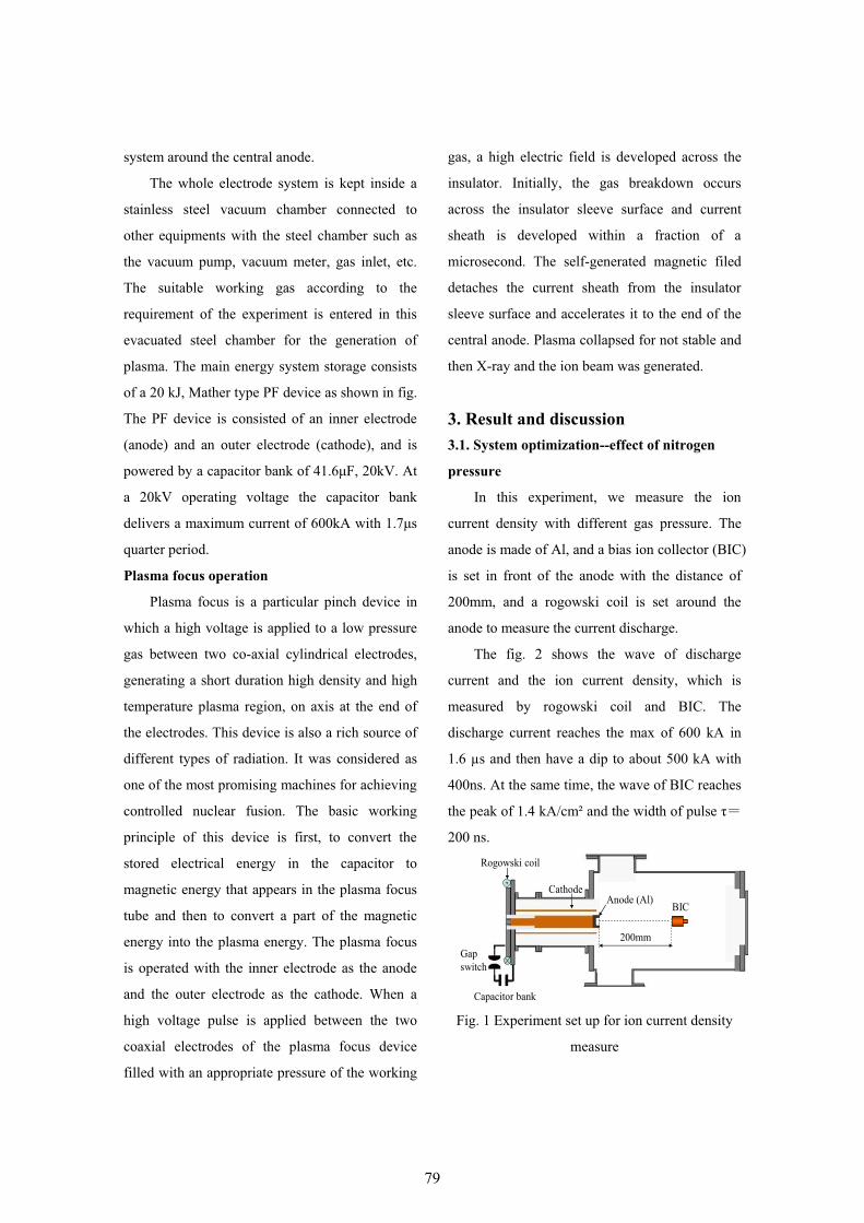
system around the central anode.
The whole electrode system is kept inside a
stainless steel vacuum chamber connected to
other equipments with the steel chamber such as
the vacuum pump, vacuum meter, gas inlet, etc.
The suitable working gas according to the
requirement of the experiment is entered in this
evacuated steel chamber for the generation of
plasma. The main energy system storage consists
of a 20 kJ, Mather type PF device as shown in fig.
The PF device is consisted of an inner electrode
(anode) and an outer electrode (cathode), and is
powered by a capacitor bank of 41.6�F, 20kV. At
a 20kV operating voltage the capacitor bank
delivers a maximum current of 600kA with 1.7�s
quarter period.
Plasma focus operation
Plasma focus is a particular pinch device in
which a high voltage is applied to a low pressure
gas between two co-axial cylindrical electrodes,
generating a short duration high density and high
temperature plasma region, on axis at the end of
the electrodes. This device is also a rich source of
different types of radiation. It was considered as
one of the most promising machines for achieving
controlled nuclear fusion. The basic working
principle of this device is first, to convert the
stored electrical energy in the capacitor to
magnetic energy that appears in the plasma focus
tube and then to convert a part of the magnetic
energy into the plasma energy. The plasma focus
is operated with the inner electrode as the anode
and the outer electrode as the cathode. When a
high voltage pulse is applied between the two
coaxial electrodes of the plasma focus device
filled with an appropriate pressure of the working
gas, a high electric field is developed across the
insulator. Initially, the gas breakdown occurs
across the insulator sleeve surface and current
sheath is developed within a fraction of a
microsecond. The self-generated magnetic filed
detaches the current sheath from the insulator
sleeve surface and accelerates it to the end of the
central anode. Plasma collapsed for not stable and
then X-ray and the ion beam was generated.
3. Result and discussion 3.1. System optimization--effect of nitrogen
pressure
In this experiment, we measure the ion
current density with different gas pressure. The
anode is made of Al, and a bias ion collector (BIC)
is set in front of the anode with the distance of
200mm, and a rogowski coil is set around the
anode to measure the current discharge.
The fig. 2 shows the wave of discharge
current and the ion current density, which is
measured by rogowski coil and BIC. The
discharge current reaches the max of 600 kA in
1.6 μs and then have a dip to about 500 kA with
400ns. At the same time, the wave of BIC reaches
the peak of 1.4 kA/cm² and the width of pulse �
200 ns.
Fig. 1 Experiment set up for ion current density
measure
200mm
Capacitor bank
Anode (Al)BIC
Rogowski coil
Cathode
Gap switch
7979
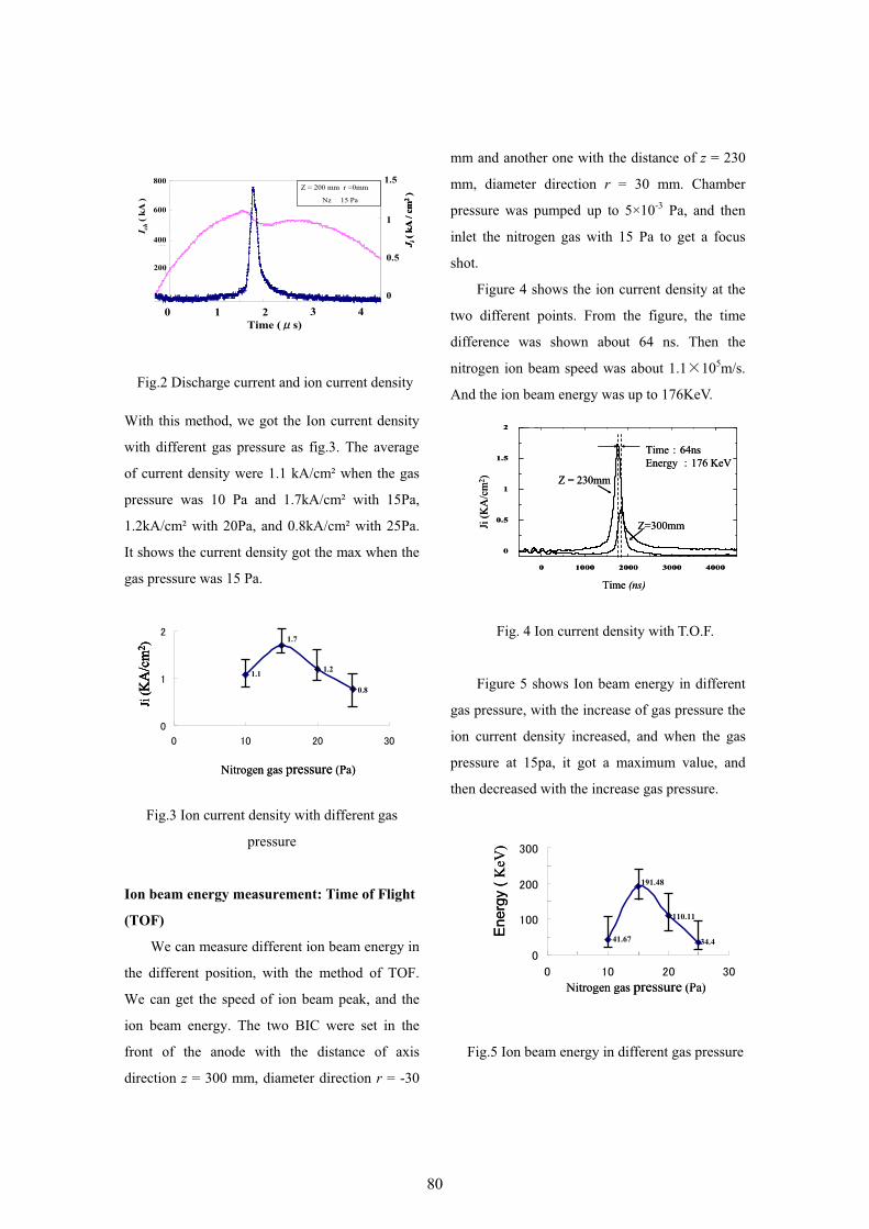
With this method, we got the Ion current density
with different gas pressure as fig.3. The average
of current density were 1.1 kA/cm² when the gas
pressure was 10 Pa and 1.7kA/cm² with 15Pa,
1.2kA/cm² with 20Pa, and 0.8kA/cm² with 25Pa.
It shows the current density got the max when the
gas pressure was 15 Pa.
Fig.3 Ion current density with different gas
pressure
Ion beam energy measurement: Time of Flight
(TOF)
We can measure different ion beam energy in
the different position, with the method of TOF.
We can get the speed of ion beam peak, and the
ion beam energy. The two BIC were set in the
front of the anode with the distance of axis
direction z = 300 mm, diameter direction r = -30
mm and another one with the distance of z = 230
mm, diameter direction r = 30 mm. Chamber
pressure was pumped up to 5×10⁻³ Pa, and then
inlet the nitrogen gas with 15 Pa to get a focus
shot.
Figure 4 shows the ion current density at the
two different points. From the figure, the time
difference was shown about 64 ns. Then the
nitrogen ion beam speed was about 1.1 105m/s.
And the ion beam energy was up to 176KeV.
Fig. 4 Ion current density with T.O.F.
Figure 5 shows Ion beam energy in different
gas pressure, with the increase of gas pressure the
ion current density increased, and when the gas
pressure at 15pa, it got a maximum value, and
then decreased with the increase gas pressure.
Fig.5 Ion beam energy in different gas pressure
Nitrogen gas pressure (Pa)
Ji(K
A/c
m2 )
0.8
1.2
1.7
1.1
Nitrogen gas pressure (Pa)
Ji(K
A/c
m2 )
0.8
1.2
1.7
1.1
Ji(K
A/c
m2 )
Ji(K
A/c
m2 )
0.8
1.2
1.7
1.1
800
600
400
0 1 2 3 40
0.5
1
1.5
200
Time ( s)
I ch
( kA
)
J i( k
A /
cm2
)
Z = 200 mm r =0mm
N 15 Pa
800
600
400
0 1 2 3 40
0.5
1
1.5
200
Time ( s)
I ch
( kA
)
J i( k
A /
cm2
)
Z = 200 mm r =0mm
N 15 Pa
0 1000 2000 3000 4000
0
0.5
1
1.5
2
Time (ns)
Z = 230mm
Z=300mm
Time 64nsEnergy 176 KeV
Ji(K
A/c
m2 )
0 1000 2000 3000 4000
0
0.5
1
1.5
2
Time (ns)
Z = 230mm
Z=300mm
Time 64nsEnergy 176 KeV
Ji(K
A/c
m2 )
Ener
gy(K
eV)
Nitrogen gas pressure (Pa)
34.4
110.11
191.48
41.67Ener
gy(K
eV)
Nitrogen gas pressure (Pa)
34.4
110.11
191.48
41.67
Fig.2 Discharge current and ion current density
8080
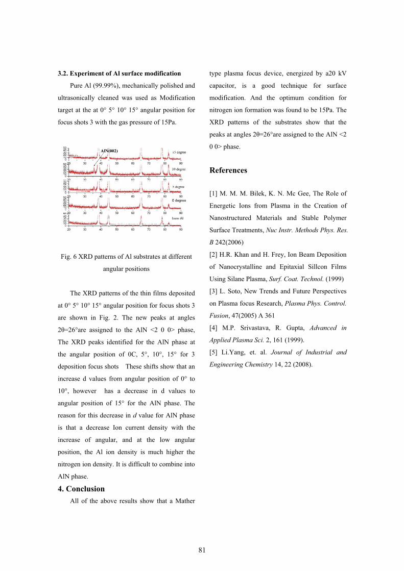
3.2. Experiment of Al surface modification
Pure Al (99.99%), mechanically polished and
ultrasonically cleaned was used as Modification
target at the at 0° 5° 10° 15° angular position for
focus shots 3 with the gas pressure of 15Pa.
Fig. 6 XRD patterns of Al substrates at different
angular positions
The XRD patterns of the thin films deposited
at 0° 5° 10° 15° angular position for focus shots 3
are shown in Fig. 2. The new peaks at angles
2�=26°are assigned to the AlN <2 0 0> phase,
The XRD peaks identified for the AlN phase at
the angular position of 0C, 5°, 10°, 15° for 3
deposition focus shots These shifts show that an
increase d values from angular position of 0° to
10°, however has a decrease in d values to
angular position of 15° for the AlN phase. The
reason for this decrease in d value for AlN phase
is that a decrease Ion current density with the
increase of angular, and at the low angular
position, the Al ion density is much higher the
nitrogen ion density. It is difficult to combine into
AlN phase.
4. Conclusion All of the above results show that a Mather
type plasma focus device, energized by a20 kV
capacitor, is a good technique for surface
modification. And the optimum condition for
nitrogen ion formation was found to be 15Pa. The
XRD patterns of the substrates show that the
peaks at angles 2�=26°are assigned to the AlN <2
0 0> phase.
References
[1] M. M. M. Bilek, K. N. Mc Gee, The Role of
Energetic Ions from Plasma in the Creation of
Nanostructured Materials and Stable Polymer
Surface Treatments, Nuc Instr. Methods Phys. Res.
B 242(2006)
[2] H.R. Khan and H. Frey, Ion Beam Deposition
of Nanocrystalline and Epitaxial Sillcon Films
Using Silane Plasma, Surf. Coat. Technol. (1999)
[3] L. Soto, New Trends and Future Perspectives
on Plasma focus Research, Plasma Phys. Control.
Fusion, 47(2005) A 361
[4] M.P. Srivastava, R. Gupta, Advanced in
Applied Plasma Sci. 2, 161 (1999).
[5] Li.Yang, et. al. Journal of Industrial and
Engineering Chemistry 14, 22 (2008).
AlN(002)AlN(002)
8181
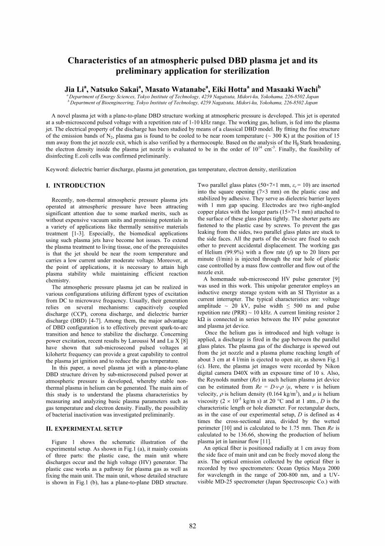
Characteristics of an atmospheric pulsed DBD plasma jet and its preliminary application for sterilization
Jia Lia, Natsuko Sakaia, Masato Watanabea, Eiki Hottaa and Masaaki Wachiba Department of Energy Sciences, Tokyo Institute of Technology, 4259 Nagatsuta, Midori-ku, Yokohama, 226-8502 Japan b Department of Bioengineering, Tokyo Institute of Technology, 4259 Nagatsuta, Midori-ku, Yokohama, 226-8502 Japan
A novel plasma jet with a plane-to-plane DBD structure working at atmospheric pressure is developed. This jet is operated
at a sub-microsecond pulsed voltage with a repetition rate of 1-10 kHz range. The working gas, helium, is fed into the plasma jet. The electrical property of the discharge has been studied by means of a classical DBD model. By fitting the fine structure of the emission bands of N2, plasma gas is found to be cooled to be near room temperature (~ 300 K) at the position of 15 mm away from the jet nozzle exit, which is also verified by a thermocouple. Based on the analysis of the H Stark broadening, the electron density inside the plasma jet nozzle is evaluated to be in the order of 1014 cm-3. Finally, the feasibility of disinfecting E.coli cells was confirmed preliminarily.
Keyword: dielectric barrier discharge, plasma jet generation, gas temperature, electron density, sterilization
I. INTRODUCTION
Recently, non-thermal atmospheric pressure plasma jets operated at atmospheric pressure have been attracting significant attention due to some marked merits, such as without expensive vacuum units and promising potentials in a variety of applications like thermally sensitive materials treatment [1-3]. Especially, the biomedical applications using such plasma jets have become hot issues. To extend the plasma treatment to living tissue, one of the prerequisites is that the jet should be near the room temperature and carries a low current under moderate voltage. Moreover, at the point of applications, it is necessary to attain high plasma stability while maintaining efficient reaction chemistry.
The atmospheric pressure plasma jet can be realized in various configurations utilizing different types of excitation from DC to microwave frequency. Usually, their generation relies on several mechanisms: capacitively coupled discharge (CCP), corona discharge, and dielectric barrier discharge (DBD) [4-7]. Among them, the major advantage of DBD configuration is to effectively prevent spark-to-arc transition and hence to stabilize the discharge. Concerning power excitation, recent results by Laroussi M and Lu X [8] have shown that sub-microsecond pulsed voltages at kilohertz frequency can provide a great capability to control the plasma jet ignition and to reduce the gas temperature.
In this paper, a novel plasma jet with a plane-to-plane DBD structure driven by sub-microsecond pulsed power at atmospheric pressure is developed, whereby stable non-thermal plasma in helium can be generated. The main aim of this study is to understand the plasma characteristics by measuring and analyzing basic plasma parameters such as gas temperature and electron density. Finally, the possibility of bacterial inactivation was investigated preliminarily.
II. EXPERIMENTAL SETUP
Figure 1 shows the schematic illustration of the experimental setup. As shown in Fig.1 (a), it mainly consists of three parts: the plastic case, the main unit where discharges occur and the high voltage (HV) generator. The plastic case works as a pathway for plasma gas as well as fixing the main unit. The main unit, whose detailed structure is shown in Fig.1 (b), has a plane-to-plane DBD structure.
Two parallel glass plates (50×7×1 mm, �r = 10) are inserted into the square opening (7×3 mm) on the plastic case and stabilized by adhesive. They serve as dielectric barrier layers with 1 mm gap spacing. Electrodes are two right-angled copper plates with the longer parts (15×7×1 mm) attached to the surface of these glass plates tightly. The shorter parts are fastened to the plastic case by screws. To prevent the gas leaking from the sides, two parallel glass plates are stuck to the side faces. All the parts of the device are fixed to each other to prevent accidental displacement. The working gas of Helium (99.9%) with a flow rate (f) up to 20 liters per minute (l/min) is injected through the rear hole of plastic case controlled by a mass flow controller and flow out of the nozzle exit.
A homemade sub-microsecond HV pulse generator [9] was used in this work. This unipolar generator employs an inductive energy storage system with an SI Thyristor as a current interrupter. The typical characteristics are: voltage amplitude ~ 20 kV, pulse width 500 ns and pulse repetition rate (PRR) ~ 10 kHz. A current limiting resistor 2 k� is connected in series between the HV pulse generator and plasma jet device.
Once the helium gas is introduced and high voltage is applied, a discharge is fired in the gap between the parallel glass plates. The plasma gas of the discharge is spewed out from the jet nozzle and a plasma plume reaching length of about 3 cm at 4 l/min is ejected to open air, as shown Fig.1 (c). Here, the plasma jet images were recorded by Nikon digital camera D40X with an exposure time of 10 s. Also, the Reynolds number (Re) in such helium plasma jet device can be estimated from Re = D�v�� /�, where v is helium velocity, � is helium density (0.164 kg/m3), and � is helium viscosity (2 10-5 kg/m s) at 20 �C and at 1 atm., D is the characteristic length or hole diameter. For rectangular ducts, as in the case of our experimental setup, D is defined as 4 times the cross-sectional area, divided by the wetted perimeter [10] and is calculated to be 1.75 mm. Then Re is calculated to be 136.66, showing the production of helium plasma jet in laminar flow [11].
An optical fiber is positioned radially at 1 cm away from the side face of main unit and can be freely moved along the axis. The optical emission collected by the optical fiber is recorded by two spectrometers: Ocean Optics Maya 2000 for wavelength in the range of 200-800 nm, and a UV-visible MD-25 spectrometer (Japan Spectroscopic Co.) with
8282
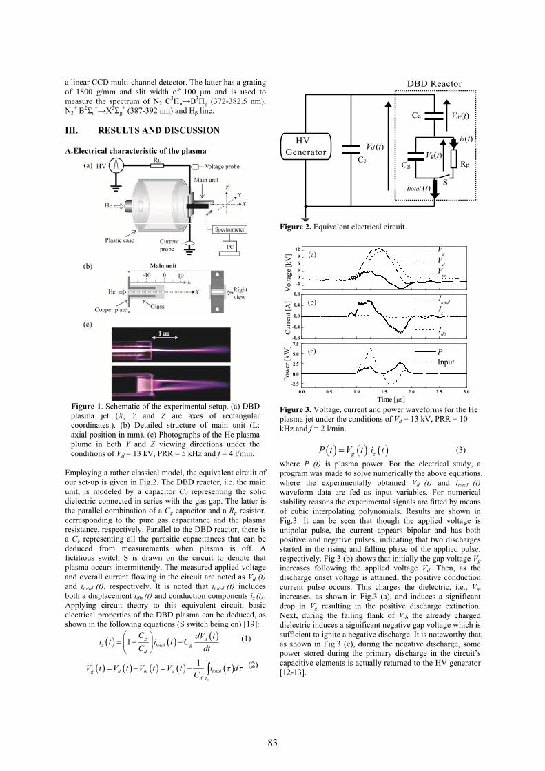
a linear CCD multi-channel detector. The latter has a grating of 1800 g/mm and slit width of 100 �m and is used to measure the spectrum of N2 C3�u�B3�g (372-382.5 nm), N2
+ B2 u+�X2 g
+ (387-392 nm) and H line.
III. RESULTS AND DISCUSSION
A.Electrical characteristic of the plasma
Figure 1. Schematic of the experimental setup. (a) DBD plasma jet (X, Y and Z are axes of rectangular coordinates.). (b) Detailed structure of main unit (L: axial position in mm). (c) Photographs of the He plasma plume in both Y and Z viewing directions under the conditions of Vd = 13 kV, PRR = 5 kHz and f = 4 l/min.
Employing a rather classical model, the equivalent circuit of our set-up is given in Fig.2. The DBD reactor, i.e. the main unit, is modeled by a capacitor Cd representing the solid dielectric connected in series with the gas gap. The latter is the parallel combination of a Cg capacitor and a Rp resistor, corresponding to the pure gas capacitance and the plasma resistance, respectively. Parallel to the DBD reactor, there is a Cc representing all the parasitic capacitances that can be deduced from measurements when plasma is off. A fictitious switch S is drawn on the circuit to denote that plasma occurs intermittently. The measured applied voltage and overall current flowing in the circuit are noted as Vd (t) and itotal (t), respectively. It is noted that itotal (t) includes both a displacement idis (t) and conduction components iz (t). Applying circuit theory to this equivalent circuit, basic electrical properties of the DBD plasma can be deduced, as shown in the following equations (S switch being on) [19]:
� � � � � �1 g dz total g
d
C dV ti t i t C
C dt� �
� � �� �� �
(1)
� � � � � � � � � �0
1 t
g d m d totald t
V t V t V t V t i dC
� �� � � � � (2)
HVGenerator
DBD Reactor
Cg Rp
Cd
Vd (t)
itotal (t)
iz(t)
Vg(t)
Vm(t)
S
Cc
Figure 2. Equivalent electrical circuit.
0.0 0.5 1.0 1.5 2.0 2.5 3.0-2.5
0.0
2.5
5.0
7.5
P Input
Time [�s]
Pow
er [k
W]
-0.8
-0.4
0.0
0.4
0.8 Itotal Iz
Idis Curre
nt [A
]-30369
12 Vg Vd Vm
(c)
(b)
(a)
Vol
tage
[kV
]
Figure 3. Voltage, current and power waveforms for the He plasma jet under the conditions of Vd = 13 kV, PRR = 10 kHz and f = 2 l/min.
� � � � � �g zP t V t i t� (3)
where P (t) is plasma power. For the electrical study, a program was made to solve numerically the above equations, where the experimentally obtained Vd (t) and itotal (t) waveform data are fed as input variables. For numerical stability reasons the experimental signals are fitted by means of cubic interpolating polynomials. Results are shown in Fig.3. It can be seen that though the applied voltage is unipolar pulse, the current appears bipolar and has both positive and negative pulses, indicating that two discharges started in the rising and falling phase of the applied pulse, respectively. Fig.3 (b) shows that initially the gap voltage Vg increases following the applied voltage Vd. Then, as the discharge onset voltage is attained, the positive conduction current pulse occurs. This charges the dielectric, i.e., Vm increases, as shown in Fig.3 (a), and induces a significant drop in Vg resulting in the positive discharge extinction. Next, during the falling flank of Vd, the already charged dielectric induces a significant negative gap voltage which is sufficient to ignite a negative discharge. It is noteworthy that, as shown in Fig.3 (c), during the negative discharge, some power stored during the primary discharge in the circuit’s capacitive elements is actually returned to the HV generator [12-13].
8383
B. Plasma emission To investigate what kinds of excited species presented in
the plasma, the aforementioned spectrometer (Maya 2000) is used to measure the optical emission of plasma plume. All spectral plots are the result of 5 data acquisitions. Spectral
species identification, labeling and relative intensity measurements were done by using the Spectrum Analyzer
(version 1.7) software [14]. A typical emission spectrum of the helium plasma in the
range of 200-800 nm obtained at the nozzle exit (L = 0 mm) is shown in Fig. 4. It shows that there are strong nitrogen molecular lines as well as a few helium and oxygen atomic lines. The strongest emission is the excited He atom line at 706.5 nm, and N2 (C3�u�B3�g) band at 337.1 nm and excited oxygen line (3p 5P �3s 5S) at 777.3 nm are shown.
Oxygen and nitrogen species arise because the plasma is ejected into the ambient air where its energetic electrons and He metastables ionize and excite air molecules. The N2
+ line at 391.4 nm is attributed to Penning ionization and charge transfer [15] followed by direct electron-impact excitation. Atomic oxygen is generally generated by a dissociative collision between an oxygen molecule and an electron. Atomic oxygen may also be generated though Penning ionization [16]. Moreover, the emission band of the OH radical at 308.9 nm is shown in the spectrum. The OH radicals represent the result of the dissociation of H2O molecules from the humid back-diffused air caused by collisions with accelerated electrons or with long-lived species present in the plasma, especially helium metastables[17].
To observe qualitatively the behavior of the plasma species along the axial direction, we selected four representative lines: He – 706.5 nm as plasma gas, N2 – 337.1 nm as the dominant component of the diffusing air, O – 777.4 nm as species crucial for biomedical treatment and N2
+ – 391.4 nm as an indicator of helium metastable presence.
Figure 5 portrays the peak intensity of selected emission line as a function of axial position L. For better distinction, the emission intensity of the species other than He is normalized to 1/5 of the peak intensity of He 706.5 nm line. As can be seen, the He 706.5 nm decays as soon as the plasma plume propagates out of the discharge zone between parallel electrodes (L � -5 mm). The reason may be due to its high excitation energy (23.07 eV) and thus sensitive to the intensity of electric field. The emissions of the air originating species (N2
+, O) present peaks at the same position, the nozzle exit ( i.e. L = 0 mm). This is the place corresponding to the most favorable combination between the electric field strength and the back-diffusion of air into the plasma column to excite the species. Inside the jet nozzle, although the electric field is very intense, the back-diffusion of air is low, and away from the jet nozzle the back-diffusion of air is high while the electric field strength decreases. The N2 337.1 nm line increases slowly and reaches its maximum at about 5 mm away from the nozzle exit. This may be explained as follows. The threshold energy of N2 (C3�u) state is much lower than that of N2
+
(B2 u+) and O (3p 5P). Therefore, N2 (C3�u) state can still be
generated through various processes such as step excitation and pooling reaction (2N2 (A3 u
+) � N2 (C3�u) + N2 (X1 g
+)) [18]. This process was found to be the dominant production mechanism of the C-state in the afterglow of He/N2 plasmas in DBD at atmospheric pressure [19].
-20 -15 -10 -5 0 5 10
0.0
0.2
0.4
0.6
0.8
1.0
He (706.5 nm) O (777.4 nm)
Inte
nsity
[a.u
.]
Axial position L [mm]
N2 (C) (337.1 nm) N2
+ (391.4 nm)
Figure 5. Dependence of selected N2 (C), N2+, He and
O atom normalized line intensities on the axial position L. Experimental conditions are same as that of Fig.4.
C. Excitation temperature and Gas temperature To have a further insight into the plasma characteristics,
the excitation temperature is obtained provided that the population in the levels of atom follows the Boltzmann distribution for plasma in the local thermodynamic equilibrium. Based on the optical emission spectrum shown in Fig.4, the characteristic spectral lines 587.56, 667.82, 706.5, and 728.13 of He atoms are chosen for approximation. After calculation, the Texc is found to be around 1123 K.
Gas temperature Tg is another important parameter to evaluate non-thermal plasma behavior and some parameters, like electron density, are dependent on Tg. Also, it is quite important when plasmas are to be applied to biomedical processing. Generally, Tg increases with applied voltage and pulse repetition rate while decreases with flow rate.
For non-thermal plasma, Tg can be usually deduced from the rotational temperature Tr of diatomic species, such as N2, N2
+ and OH. The rotational temperature describes the population of the rotational levels in molecular species. The distribution, unlike that of vibrational levels, is not given by a pure Boltzmann distribution. Each rotational level has a different statistical weight due to the (2J+1)-fold degeneracy of the states, where J is the total angular momentum of the molecule. Therefore, the thermal distribution of the rotational states will be given by the product of the Boltzmann factor exp(-E/kT) times the statistical weight (2J+1) [20]. For most species it can be assumed that Tr is
200 300 400 500 600 700 8000
2000
4000
6000
8000
NO
He
667.
8
He 706.5
O 7
77.4
He
728.
1
H�
He
587.
5
N2+ 3
91.4
N2(C) 337.1
OH
308
.9
Inte
nsity
[a.u
.]
Wavelength [nm]Figure 4. Emission spectra at the axial position L=0 mm under the conditions of Vd = 13 kV, PRR = 10 kHz and f = 2 l/min.
8484
close to the translational temperature Tt and is effectively considered to be Tg of the mixture because rotational-to-translational relaxation is fast at atmospheric pressure [15, 21, 22, 23]. Since the MD-25 spectrometer used in this paper does not resolve the rotational structure, in order to calculate the rotational temperature, we have fitted the experimental data with a theoretical calculation that takes into account the instrumental line broadening of the spectrometer.
In this work, to determine the gas temperature, the MD-25 spectrometer was used to measure the emission of N2 C3�u-B3�g (�v = -2) band at the position L = 15 mm and then the Specair program [22, 24] was used to generate the simulated spectra and for comparison, both experimental and simulated spectra were normalized. A least-square procedure was made to obtain the best fit, which gives the rotational temperature. A typical fitting of the measured band spectrum with the simulated one is shown in Fig.6. By this way, it is found that gas temperature is already cooled to be around room temperature (300 K) at the position 15 mm away from the nozzle outlet. The gas temperature obtained from this method is in good agreement with the value (301.75 ± 0.8 K) measured by the thermocouple (CIE 305P) with a nominal error of 0.1�C. By applying the same method to simulate the emission of N2
+ (B2 u+�X2 g
+) band,
366 369 372 375 378 3810.00.20.40.60.81.0 Simulated spectrum
Inte
nsity
[a.u
.]
Wavelength [nm]
Experimental spectrum
3-52-4
1-3
0-2
Best fitTr = 300 K
Figure 6. Experimental and simulated best-fit spectra of N2 (C3�u�B3�g) at L = 15 mm. Experimental conditions are: Vd = 13 kV, PRR = 10 kHz , f = 2 l/min.
the gas temperature inside the plasma jet was determined to be in the range of 360 ~ 400 K. These results will be used to calculate electron density in the next section.
D. Electron density The spectral method for obtaining the electron density is
based on the analysis of the profile broadening of the 486.13 nm H line. Compared to other hydrogen Balmer lines, the H line is often preferred because it has adequate emission intensity, higher sensitivity to electron density and lower susceptibility to self-absorption [25]. Besides the Stark broadening, the H line emitted from plasma (usually mixed with a little H2) can be broadened by other mechanisms and the total broadening of the line profile is due to the combined contribution of all effects. Each broadening mechanism is independent and plays a different role on broadening the line depending on the plasma conditions. Under the experimental conditions of this work (1 atm, Tg ~ 360-400K), the only relevant sources of broadening are the Stark broadening, the van der Waals broadening, the Doppler broadening and the instrumental broadening. Other less important effects such as resonance broadening can be ignored due to the small amount of H2 addition.
The total H lineshape can be approximated with a Voigt function, resulting from a convolution of Gaussian and Lorentzian profiles. The full-width at half maximum
(FWHM) of both the Gaussian and Lorentzian components, ��G and ��L, are given in Eq. (4) and (5), respectively
2 2G Doppler Instrument� � �� � � � � (4)
L VanderWaals Stark� � �� � � � � (5)
where ��Doppler, ��Instrument, ��Van der Waals and ��Stark are the FWHM of Doppler, instrumental, Van der Waals and Stark broadening, respectively. The part of the line broadening corresponding only to the Stark broadening can be obtained from the total broadened profile.
During the experiment, a small amount of H2 (0.02 mol%) was added into the He gas flow and the emission emitted from plasma was recorded. The instrumental broadening was calibrated with the He–Ne laser (5 mW) on steady glow 632.8 nm, using the same experimental set-up (1800 grooves/mm gratings) and was found to be a Gaussian of FWHM 0.359 nm. Doppler broadening is due to the thermal motion of excited hydrogen atoms and is determined from the gas temperature Tg by the expression of its FWHM
0.5
707.16 10 g
Doppler
TM
� �� � �� � � �
� � (6)
where �0 is the emission wavelength in nm and M is the atomic weight of H atoms in gmol�1. Van der Waals broadening is caused by collisions of excited H atoms (the emitters) with ground state He atoms (the perturbers). According to [21], the value of ��Van der Waals was estimated by formula
� �3/10
2/513 2 204.09 10 g
Vander Waals He
TR n� � �
�� � �
� � � �� �
(7)
where � is the average polarizability of He, given in cm3, and is equal to 1.38×a0
3 (a0 is the Bohr radius in cm), the parameter R2 � 600 × a0
2 cm2 is determined from the ionization energy of H and the upper and lower energy levels of the H, � = 0.8 is the emitter-perturber reduced mass, and nHe is the neutral He gas density in cm�3. Stark broadening arises from the interaction between charged particles and excited H atoms, and the FWHM of Stark broadening is related to the electron density by [26]
� � � �2/3112 10Stark enm n� �� � (8)
where ne is the electron density in cm�3. The electron temperature is not considered since the electron density depends scarcely on the electron temperature for the H line.
The recorded H spectral profile was normalized to its area and then fitted to a Voigt function according to the Maquardt–Levenberg method. ��G, calculated from equation (4), was kept constant at a given gas temperature. ��L was obtained from the best fit between the simulated Voigt profile and the experimental spectrum. Then, the Stark contribution, ��Stark, was found from equation (5). A typical fitting is shown in Fig.7, where ne = 1.52×1014 cm-3 is obtained from ��Stark = 0.0571 nm.
By this way, the effects of peak applied voltage, pulse repetition rate, flow rate and axial position on electron density are investigated. Results are shown in Fig.8. Electron density increases almost linearly with the pulse repetition rate and applied voltage, as shown in Fig.8 (a). With the increase of pulse repetition rate or applied voltage, electrons can gain more energy and cause more ionization collisions. On the other hand, from Fig.8 (b), it can be seen
8585
484.5 485 485.5 486 486.5 487 487.50
0.2
0.4
0.6
0.8
1
Inte
nsity
[a.u
.]
Wavelength [nm]
H line Measured Voigit fit
Figure 7. A typical line profile of H line at the position of L = -10 mm under the conditions of Vd = 8 kV, PRR = 10 kHz and f = 2 l/min. ��Stark = 0.0571 nm and electron density ne = 1.52×1014 cm-3.
that electron density varies inversely with the He gas flow rate. A same behavior was also found in Ar plasma jet [26]. With the increased flow rates, the gas velocity increases and the residence time of the gas in the electrode gap decreases. Consequently, the electron density becomes lower.
Figure 8 (c) reveals the electron density as a function of axial position. The pulse repetition rate was set to be 5 and 10 kHz under the conditions of 13 kV and 2 l/min. As shown in Fig.8 (c), the electron density rapidly decreases as the position is approaching the nozzle exit, due to recombination and attachment. At the position of the nozzle exit, the electron density has been 3~4 times less than that in the center of jet nozzle. Electron density away from the nozzle exit could not be determined due to the limitation of the spectrometer used here; it is reasonable to estimate that the electron density in the plasma plume should be lower, probably in the order of 1013 cm-3. However, its confirmation needs further investigations.
E. Sterilization experiment
To confirm the feasibility of disinfecting micro-organisms, we employed the E.coli bacterial cells as a model micro-organism. The plasma jet was directed to the center of the Petri dish perpendicularly to its surface. The distance between surface of agar and outlet edge of plasma nozzle was 2 cm. The operational conditions were set to be f = 2 l/min, PRR = 5 kHz and Vd = 13 kV. Figure 9 presents photos of Petri dishes of 90 mm diameter, showing the distribution of bacteria population of E. coli on agar. It was taken after incubation over 24 h at 37 °C. Before incubation, E. coli was treated with plasma jet under exposure time of 4 and 8 min, respectively. By contrast with untreated culture medium growing E.coli, the inactivation effect is clearly seen.
Figure 8. (a) The variation in the electron density with peak applied voltage at different pulse repetition rate. Experimental condition: f = 2 l/min; (b) The variation in the electron density with pulse repetition rate at serial of He gas flow rate of 2 and 3 l/min. Experimental condition: Vd = 13 kV; (c) The variation in the electron density with axial position at different pulse repetition rate. Experimental condition: f = 2 l/min and Vd = 13 kV.
(a) (b) (c)
(d) (e) (f)
Figure 9. E.coli growth represented in terms of CFUs on agar plates, where (a) and (d) control without plasma treatment, (b) and (e) treated with 4 min and (c) and (f) treated with 8 min. CFU: (a) - (c) 5×10³ (d)-(f) 5×10⁴ .
8686
IV. SUMMARY
A novel plasma jet with a plane-to-plane DBD structure working at atmospheric pressure is developed to create non-thermal plasma. This jet is operated at a pulsed voltage, produced by a homemade sub-microsecond pulsed power generator, with a repetition rate of 1-10 kHz range. The working gas, helium for the moment, is fed into the plasma jet. The electrical property of the discharge has been studied by means of a classical DBD model. By fitting the fine structure of the emission bands of N2
+ and N2, plasma gas is found to be heated inside the jet nozzle up to ~ 400 K but is cooled during transport from the nozzle exit. At the position of 15 mm away from the jet nozzle exit, the gas has been cooled to be near room temperature (~ 300 K), which is also verified by a thermocouple. The electron density is evaluated from the analysis of the Stark broadening of H emission and found to be in the order of 1014 cm-3 inside the plasma jet nozzle. It is shown that the electron density increases almost linearly with the applied voltage and pulse repetition rate while decays rapidly as plasma moves towards the nozzle exit. Finally, preliminary results show that this jet has potential in bacterial inactivation.
REFERENCES
[1] F. Iza, G. J. Kim, S. M. Lee, J. K. Lee, J. L. Walsh, Y. T. Zhang and M. G. Kong: “Microplasmas: Sources, particle kinetics, and biomedical applications”, Plasma Processes Polym, Vol.5, No.4, pp.322-344 (2008)
[2] M. Laroussi and T. Akan, “Arc-Free Atmospheric Pressure Cold Plasma Jets: A Review”, Plasma Processes Polym, Vol.4, No.9, pp.777-788 (2007)
[3] X. Zhang, M. Li, R. Zhou, K. Feng, and S. Yang: “Ablation of liver cancer cells in vitro by a plasma needle”, Appl. Phys. Lett. , Vol.93, No.2, pp. 021502 (2008)
[4] T. L. Ni, F. Ding, X. D. Zhu, X. H. Wen, and H. Y. Zhou: “Cold microplasma plume produced by a compact and flexible generator at atmospheric pressure”, Appl. Phys. Lett. , Vol.92, No.2, pp. 241503 (2008)
[5] H. S. Park, S. J. Kim, H. M. Joh, T. H. Chung, S. H. Bae and S. H. Leem: “Optical and electrical characterization of an atmospheric pressure microplasma jet with a capillary electrode”, Phys. Plasmas, Vol.17, No.3, pp. 033502 (2010)
[6] M. Teschke, J. Kedzierski, E. G. Finantu-Dinu, D. Korzec, and J. Engemann: “High-speed photographs of a dielectric barrier atmospheric pressure plasma jet”, IEEE Trans. Plasma Sci., Vol.33, No.2, pp. 310-311 (2005)
[7] A. Fridman, A. Chirokov, and A. Gutsol: “Non-thermal atmospheric pressure discharges”, J. Phys. D: Appl. Phys., Vol.38, No.2, pp. R1-R24 (2005)
[8] Laroussi M and Lu X: “Room-temperature atmospheric pressure plasma plume for biomedical applications”, Appl. Phys. Lett., Vol.87, No. 11, pp.113902 (2005)
[9] J. Li, N.Sakai, M. Watanabe and E. Hotta: “A 10 kHz Sub-microsecond High-voltage Pulse Generator Using SI Thyristor for Micro-plasma Jets Generation”, IEEJ Trans.FM, Vol.130, No.6, pp.573-578 (2010)
[10] http://en.wikipedia.org/wiki/Reynolds_number [11] John F.O’Hanlon: A User’s Guide to Vacuum Technology, 2nd ed, p. 23,
New York: John Wiley (1980) [12] E. Panousis, N. Merbahi, F. Clement, A.Ricard, M. Yousfi,
L.Papageorghiou, J.F. Loiseau, O.Ficheald, B.Held and N.Spyrou: “Atmospheric Pressure Dielectric Barrier Discharges Under Unipolar and Bipolar HV Excitation in View of Chemical Reactivity in Afterglow Conditions”, IEEE Trans. Plasma Sci., Vol. 37, No. 6, pp. 1004–1015 (2009)
[13] Laroussi M and Lu X: “Power consideration in the pulsed dielectric barrier discharge at atmospheric pressure”, J.Appl. Phys., Vol.96, No. 5, pp.3028-3030 (2004)
[14] Z.Navratil, D. Trunc, R. Smid and L. Lazar: “A software for optical emission spectroscopy-problem formulation and application to plasma diagnostics”,Czech. J. Phys., Vol. 56, pp.B944–B951 (2006)
[15] G.Nersisyan and W. G. Graham: “Characterization of a dielectric barrier discharge operating in an open reactor with flowing helium”, Plasma Sources Sci. Technol., Vol. 13, No.4, pp. 582-587 (2004)
[16] R.Oikari, V. Hayrinen and R. Hernberg: “Influence of N-O chemistry on the radiative emission from a direct current nitrogen plasma jet”, J. Phys. D: Appl. Phys., Vol. 35, No.11, pp. 1109-1116 (2002)
[17] S. D. Anghel, A. Simon and T. Frentiu: “Spectroscopic investigations on a low power atmospheric pressure capacitively coupled helium plasma”, Plasma Sources Sci. Technol., Vol. 17, No.4, pp. 045016(2008)
[18] I. Stefanovic, N.K. Bibinov, A.A. Deryugin, I.P. Vinogradov, A.P. Napartovich and K. Wiesemann: “Kinetics of ozone and nitric oxides in dielectric barrier discharges in O2/NOx and N2/O2/NOx mixtures”, Plasma Sources Sci. Technol.,Vol.10, No. 3, pp. 406–416 (2001)
[19] N.K. Bibinov, A.A. Fateev and K. Wiesemann: “On the influence of metastable reactions on rotational temperatures in dielectric barrier discharges in He-N2 mixtures”, J.Phys.D: Appl.Phys., Vol.34, No.12, pp.1819-1826 (2001))
[20] G. Herzberg: Molecular Spectra and Molecular Structure, 2nd ed, p. 124, New York: Van Nostrand(1950)
[21] Q.Wang,I. Koleva, V. M. Donnelly and D. J. Economou: “Spatially resolved diagnostics of an atmospheric pressure direct current helium microplasma”, J. Phys. D: Appl. Phys., Vol.38, No.11, pp. 1690-1697(2005)
[22] D.Staack, B. Farouk, A.F. Gutsol and A.A. Fridman: “Spectroscopic
studies and rotational and vibrational temperature measurements of atmospheric pressure normal glow plasma discharges in air”, Plasma Sources Sci. Technol., Vol. 15, No.4, pp. 818-827 (2006)
[23] D. M. Phillips: “Determination of gas temperature from unresolved bands in the spectrum from a nitrogen discharge”, J. Phys. D: Appl. Phys., Vol. 9, No.3, pp. 507-521 (1976)
[24] C.O. Laux, T.G. Spence, C.H. Kruger and R.N. Zare: “Optical diagnostics of atmospheric pressure air plasmas”,Plasma Sources Sci.Technol., Vol.12,No., pp.125-138(2003)
[25] J.M. Luque, M.D. Calzada and M. S´aez: “Experimental research into the influence of ion dynamics when measuring the electron density from the Stark broadening of the H� and H lines”, J. Phys. B: At. Mol. Opt. Phys., Vol.36, No.8, pp.1573-1584 (2003)
[26] M. Y. Qian, C. S. Ren, D. Z. Wang, J. L. Zhang and G. D. Wei: “Stark broadening measurement of the electron density in an atmospheric pressure argon plasma jet with double-power electrodes”, J.Appl. Phys., Vol.107, No. 6, pp.063303 (2010)
8787
Treatment of Zooplankton in Water by Pulsed Power − An Effect of NaHCO3 Additive for Micro Bubble Production −
Kouhei Satoh1, Masayuki Onda1, Shin-ichi Sakai2, and Go Imada2,3,*
1 Graduate School of Engineering, Niigata Institute of Technology, Japan 2 Department of Information & Electronics Engineering, Niigata Institute of Technology, Japan
3 Extreme Energy Density Research Institute, Nagaoka University of Technology, Japan
ABSTRACT Enhancement of inactivation of zooplankton in ballast water is experimentally proved inpulsed power method. A large number of micro bubbles are successfully produced by applying the pulsed power to the water with sodium hydrogen carbonate (NaHCO3)additive. The diameter and number density of bubbles are estimated to be 25 �m and 20 mm-2, respectively. Shock wave generated by burst of the bubbles inactivates the larvae of Artemia. We found that 12.5 % of the larvae of Artemia are inactivated by firing 20 shots of the pulsed power exposure, which is 2.6 times as high as that obtained for the water solution without NaHCO3 additive.
Keyword Pulsed power, Zooplankton, Ballast water, Micro bubble, Sodium hydrogen carbonate, Additive
1. Introduction Ballast water is necessary to stabilize ship's hulls during navigation. The total amount of ballast water reaches 3 to 5 billion tons a year, which is transferred internationally. Japan exports approximately 0.3 billion tons of the ballast water a year and imports 0.017 billion. The ballast water includes bacilli, microbes, eggs and larvae of marine organisms, which are undesirably discharged at a port of call. To prevent the migration of these organisms and conserve the marine environment, a international convention for the control and management of ships ballast water and sediments was adopted by the International Maritime Organization in 2004 [1]. It obligates the ships to manage their ballast water by using devices not later than 2006. Many methods for treatment of the ballast water have been studied; such as chemical, heat, sonic, magnetic, biological, radioactive and electrical treatments, however, more methods and techniques are required to develop the feasible devices.
In this study, we propose a new technique on the treatment of the larvae of zooplankton in the ballast water, which uses pulsed-power method [2]. Micro bubbles are produced by applying the pulsed power to the water. Shock wave generated by burst of the bubbles affects the life of the larvae of zooplankton. A large number of bubbles and the bubbles in small diameter are effective for the treatment of the zooplankton. To increase the number of bubbles and decrease the diameter of bubbles, in this study,sodium hydrogen carbonate, NaHCO3, is added to the water. If some energy is injected to NaHCO3 in the water, gaseous H2O and CO2 are generated as follows.
2NaHCO3 → Na2CO3 + H2O + CO2 − 136 kJ. (1)
Na2CO3 → Na2O + CO2 − 319 kJ. (2)
Na2O + H2O → 2NaOH. (3)
The reactions (1) and (2) tend to increase the number of bubbles. The solubility in water of NaHCO3 is 94 g/L at 25 °C. In addition, NaHCO3 is harmless
--------------------------------------------------------------------------------------------------------------------------------------------------------------------------------------------------------------------------------------------------------------------------------------------------------------------------------------------------------------------------------------
8888
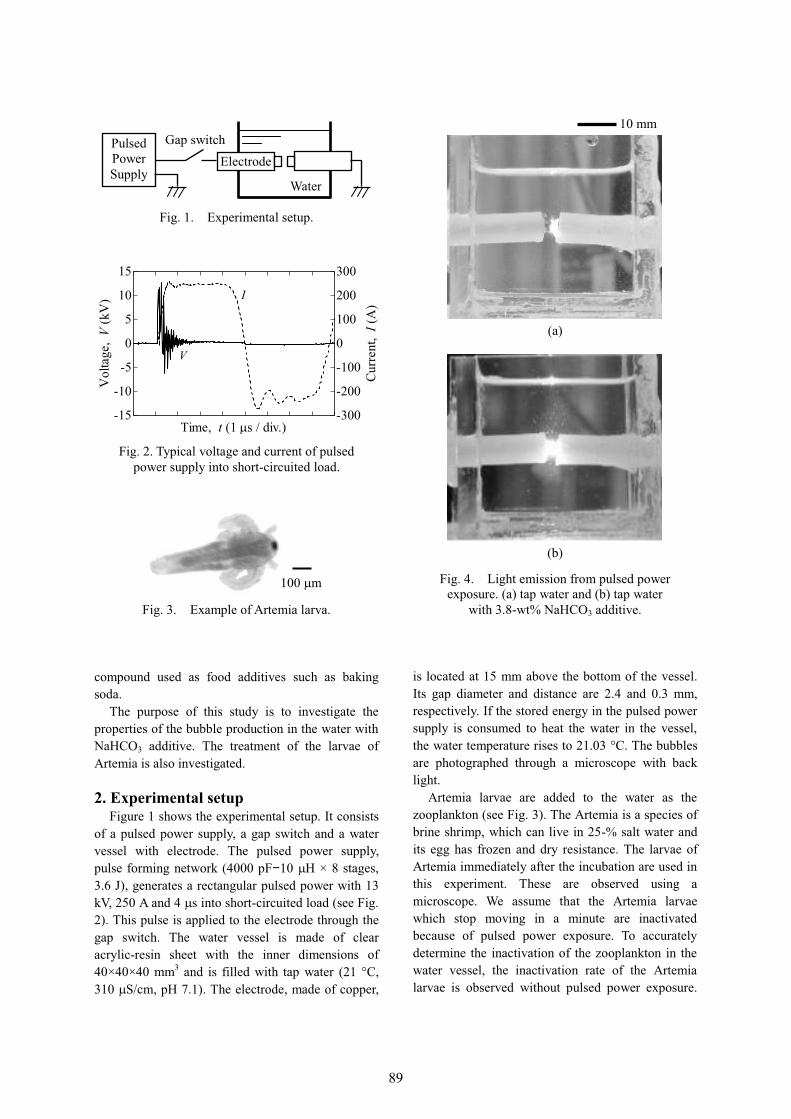
compound used as food additives such as baking soda. The purpose of this study is to investigate the properties of the bubble production in the water with NaHCO3 additive. The treatment of the larvae of Artemia is also investigated.
2. Experimental setup Figure 1 shows the experimental setup. It consists of a pulsed power supply, a gap switch and a water vessel with electrode. The pulsed power supply,pulse forming network (4000 pF−10 �H × 8 stages,3.6 J), generates a rectangular pulsed power with 13kV, 250 A and 4 �s into short-circuited load (see Fig. 2). This pulse is applied to the electrode through the gap switch. The water vessel is made of clear acrylic-resin sheet with the inner dimensions of40×40×40 mm3 and is filled with tap water (21 °C, 310 �S/cm, pH 7.1). The electrode, made of copper,
is located at 15 mm above the bottom of the vessel. Its gap diameter and distance are 2.4 and 0.3 mm,respectively. If the stored energy in the pulsed power supply is consumed to heat the water in the vessel, the water temperature rises to 21.03 °C. The bubbles are photographed through a microscope with back light. Artemia larvae are added to the water as the zooplankton (see Fig. 3). The Artemia is a species of brine shrimp, which can live in 25-% salt water and its egg has frozen and dry resistance. The larvae of Artemia immediately after the incubation are used in this experiment. These are observed using a microscope. We assume that the Artemia larvae which stop moving in a minute are inactivated because of pulsed power exposure. To accurately determine the inactivation of the zooplankton in the water vessel, the inactivation rate of the Artemia larvae is observed without pulsed power exposure.
Pulsed Power Supply
Electrode
Water
Gap switch
Fig. 1. Experimental setup.
100 �m
Fig. 3. Example of Artemia larva.
-15
-10
-5
0
5
10
15
-300
-200
-100
0
100
200
300
Time, t (1 �s / div.)
Curr
ent,
I (A
)
Vo l
tage
, V
(kV
)
V
I
Fig. 2. Typical voltage and current of pulsed power supply into short-circuited load.
10 mm
(a)
(b)
Fig. 4. Light emission from pulsed power exposure. (a) tap water and (b) tap water
with 3.8-wt% NaHCO3 additive.
8989
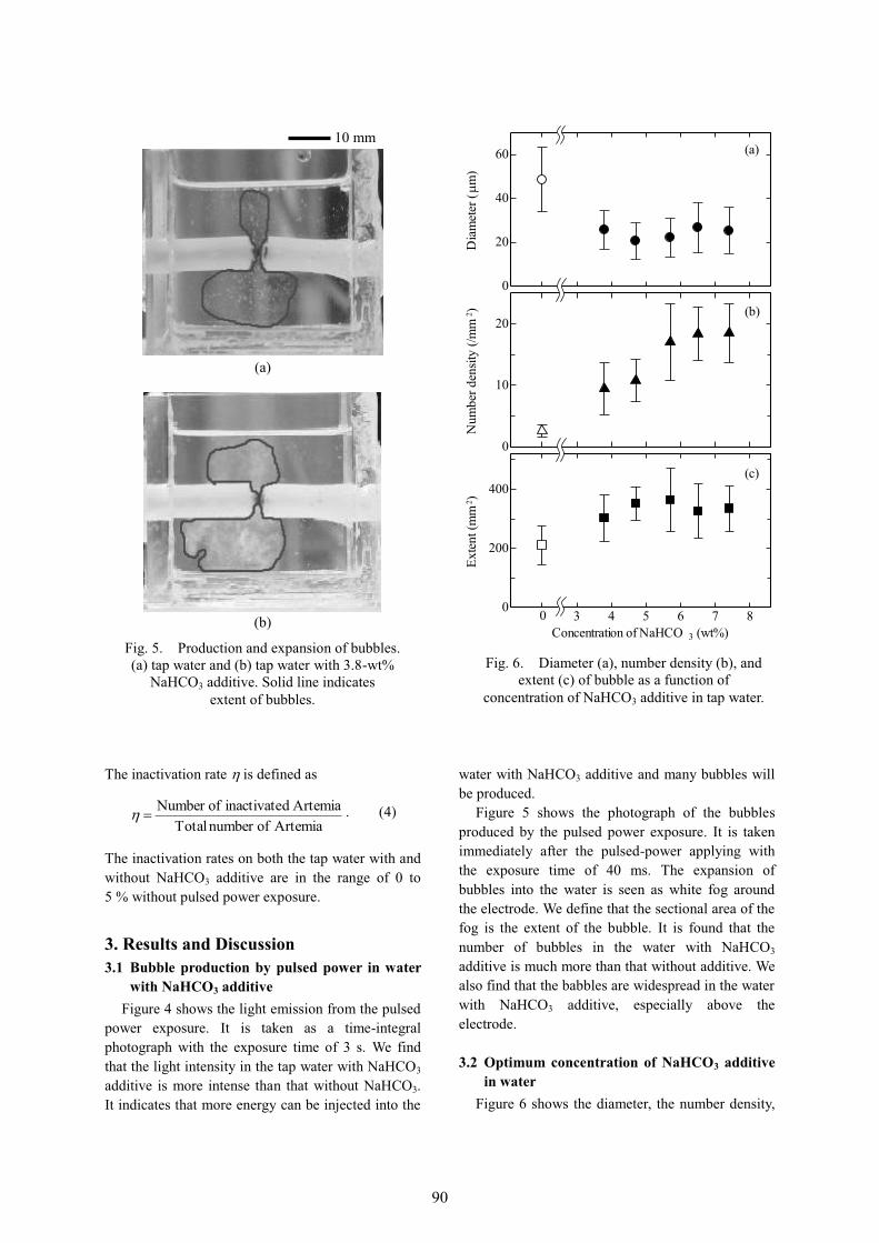
The inactivation rate � is defined as
Artemia ofnumber TotalArtemia dinactivate ofNumber
� . (4)
The inactivation rates on both the tap water with and without NaHCO3 additive are in the range of 0 to 5 % without pulsed power exposure.
3. Results and Discussion 3.1 Bubble production by pulsed power in water
with NaHCO3 additive Figure 4 shows the light emission from the pulsed power exposure. It is taken as a time-integral photograph with the exposure time of 3 s. We find that the light intensity in the tap water with NaHCO3
additive is more intense than that without NaHCO3.It indicates that more energy can be injected into the
water with NaHCO3 additive and many bubbles will be produced. Figure 5 shows the photograph of the bubbles produced by the pulsed power exposure. It is taken immediately after the pulsed-power applying with the exposure time of 40 ms. The expansion of bubbles into the water is seen as white fog around the electrode. We define that the sectional area of the fog is the extent of the bubble. It is found that the number of bubbles in the water with NaHCO3
additive is much more than that without additive. We also find that the babbles are widespread in the water with NaHCO3 additive, especially above the electrode.
3.2 Optimum concentration of NaHCO3 additive in water
Figure 6 shows the diameter, the number density,
0
10
20
Num
ber d
ensit
y (/m
m2 )
0
0
20
40
60
Dia
met
er (
�m
)
(a)
(b)
(c)
3 4 5 6 7 80
200
400
Concentration of NaHCO 3 (wt%)
Exte
nt (m
m2 )
Fig. 6. Diameter (a), number density (b), and extent (c) of bubble as a function of
concentration of NaHCO3 additive in tap water.
10 mm
(a)
(b)
Fig. 5. Production and expansion of bubbles. (a) tap water and (b) tap water with 3.8-wt%
NaHCO3 additive. Solid line indicates extent of bubbles.
9090
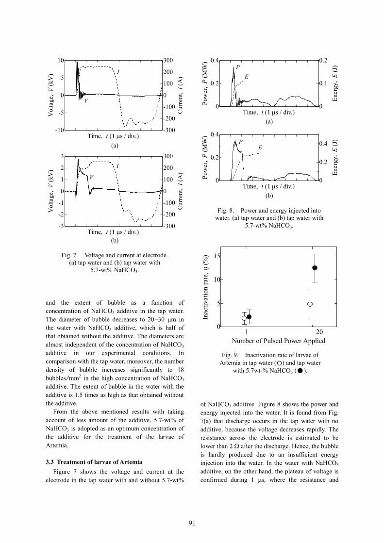
and the extent of bubble as a function of concentration of NaHCO3 additive in the tap water. The diameter of bubble decreases to 20−30 �m in the water with NaHCO3 additive, which is half of that obtained without the additive. The diameters are almost independent of the concentration of NaHCO3
additive in our experimental conditions. In comparison with the tap water, moreover, the number density of bubble increases significantly to 18 bubbles /mm2 in the high concentration of NaHCO3
additive. The extent of bubble in the water with the additive is 1.5 times as high as that obtained without the additive. From the above mentioned results with taking account of less amount of the additive, 5.7-wt% of NaHCO3 is adopted as an optimum concentration of the additive for the treatment of the larvae of Artemia.
3.3 Treatment of larvae of Artemia Figure 7 shows the voltage and current at the electrode in the tap water with and without 5.7-wt%
of NaHCO3 additive. Figure 8 shows the power and energy injected into the water. It is found from Fig. 7(a) that discharge occurs in the tap water with no additive, because the voltage decreases rapidly. The resistance across the electrode is estimated to be lower than 2 after the discharge. Hence, the bubble is hardly produced due to an insufficient energy injection into the water. In the water with NaHCO3
additive, on the other hand, the plateau of voltage is confirmed during 1 �s, where the resistance and
-10
-5
0
5
10
-300
-200
-100
0
100
200
300
Time, t (1 �s / div.)
Curr
ent,
I (A
)
Vo l
tage
, V
(kV
)
V
I
(a)
(b)
Fig. 7. Voltage and current at electrode. (a) tap water and (b) tap water with
5.7-wt% NaHCO3.
-3
-2
-1
0
1
2
3
-300
-200
-100
0
100
200
300
Time, t (1 �s / div.)
Curr
ent,
I (A
)
Vo l
tage
, V
(kV
) I
V
(a)
(b)
Fig. 8. Power and energy injected into water. (a) tap water and (b) tap water with
5.7-wt% NaHCO3.
0
0.2
0.4
0
0.1
0.2
Time, t (1 �s / div.)
Ener
gy,
E (J
)
Pow
er,
P (M
W)
EP
0
0.2
0.4
0
0.2
0.4
Time, t (1 �s / div.)
Ener
gy,
E (J
)
Pow
er,
P (M
W)
EP
Fig. 9. Inactivation rate of larvae of Artemia in tap water (�) and tap water
with 5.7wt-% NaHCO3 (●).
0
5
10
15
Number of Pulsed Power Applied
Inac
tivat
ion
rate
, ���
�
1 20
9191
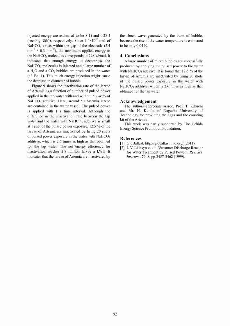
injected energy are estimated to be 8 and 0.28 J (see Fig. 8(b)), respectively. Since 9.4×10⁻⁷ mol of NaHCO3 exists within the gap of the electrode (2.4 mm� × 0.3 mmW), the maximum applied energy to the NaHCO3 molecules corresponds to 298 kJ/mol. It indicates that enough energy to decompose the NaHCO3 molecules is injected and a large number of a H2O and a CO2 bubbles are produced in the water (cf. Eq. 1). This much energy injection might cause the decrease in diameter of bubble. Figure 9 shows the inactivation rate of the larvae of Artemia as a function of number of pulsed power applied in the tap water with and without 5.7-wt% of NaHCO3 additive. Here, around 50 Artemia larvae are contained in the water vessel. The pulsed power is applied with 1 s time interval. Although the difference in the inactivation rate between the tap water and the water with NaHCO3 additive is small at 1 shot of the pulsed power exposure, 12.5 % of the larvae of Artemia are inactivated by firing 20 shots of pulsed power exposure in the water with NaHCO3
additive, which is 2.6 times as high as that obtained for the tap water. The net energy efficiency for inactivation reaches 3.8 million larvae a kWh. It indicates that the larvae of Artemia are inactivated by
the shock wave generated by the burst of bubble, because the rise of the water temperature is estimated to be only 0.04 K.
4. Conclusions A large number of micro bubbles are successfully produced by applying the pulsed power to the water with NaHCO3 additive. It is found that 12.5 % of the larvae of Artemia are inactivated by firing 20 shots of the pulsed power exposure in the water with NaHCO3 additive, which is 2.6 times as high as that obtained for the tap water.
Acknowledgement The authors appreciate Assoc. Prof. T. Kikuchi and Mr. H. Kondo of Nagaoka University of Technology for providing the eggs and the counting kit of the Artemia. This work was partly supported by The Uchida Energy Science Promotion Foundation.
References [1] GloBallast, http://globallast.imo.org/ (2011). [2] I. V. Lisitsyn et al., "Streamer Discharge Reactor
for Water Treatment by Pulsed Power", Rev. Sci. Instrum., 70, 8, pp.3457-3462 (1999).
9292
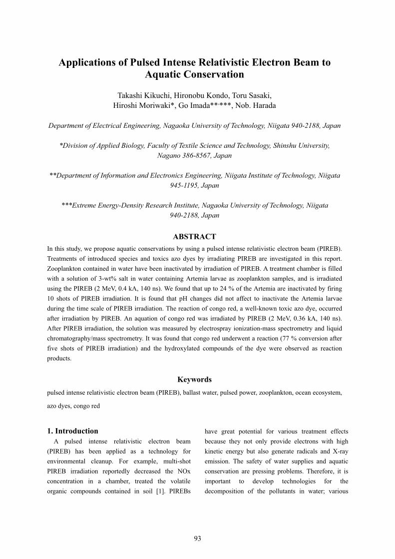
Applications of Pulsed Intense Relativistic Electron Beam to Aquatic Conservation
Takashi Kikuchi, Hironobu Kondo, Toru Sasaki,
Hiroshi Moriwaki*, Go Imada**,***, Nob. Harada
Department of Electrical Engineering, Nagaoka University of Technology, Niigata 940-2188, Japan
*Division of Applied Biology, Faculty of Textile Science and Technology, Shinshu University, Nagano 386-8567, Japan
**Department of Information and Electronics Engineering, Niigata Institute of Technology, Niigata 945-1195, Japan
***Extreme Energy-Density Research Institute, Nagaoka University of Technology, Niigata 940-2188, Japan
ABSTRACT In this study, we propose aquatic conservations by using a pulsed intense relativistic electron beam (PIREB). Treatments of introduced species and toxics azo dyes by irradiating PIREB are investigated in this report. Zooplankton contained in water have been inactivated by irradiation of PIREB. A treatment chamber is filled with a solution of 3-wt% salt in water containing Artemia larvae as zooplankton samples, and is irradiated using the PIREB (2 MeV, 0.4 kA, 140 ns). We found that up to 24 % of the Artemia are inactivated by firing 10 shots of PIREB irradiation. It is found that pH changes did not affect to inactivate the Artemia larvae during the time scale of PIREB irradiation. The reaction of congo red, a well-known toxic azo dye, occurred after irradiation by PIREB. An aquation of congo red was irradiated by PIREB (2 MeV, 0.36 kA, 140 ns). After PIREB irradiation, the solution was measured by electrospray ionization-mass spectrometry and liquid chromatography/mass spectrometry. It was found that congo red underwent a reaction (77 % conversion after five shots of PIREB irradiation) and the hydroxylated compounds of the dye were observed as reaction products.
Keywordspulsed intense relativistic electron beam (PIREB), ballast water, pulsed power, zooplankton, ocean ecosystem,
azo dyes, congo red
1. Introduction A pulsed intense relativistic electron beam (PIREB) has been applied as a technology for environmental cleanup. For example, multi-shot PIREB irradiation reportedly decreased the NOx concentration in a chamber, treated the volatile organic compounds contained in soil [1]. PIREBs
have great potential for various treatment effects because they not only provide electrons with high kinetic energy but also generate radicals and X-ray emission. The safety of water supplies and aquatic conservation are pressing problems. Therefore, it is important to develop technologies for the decomposition of the pollutants in water; various
9393
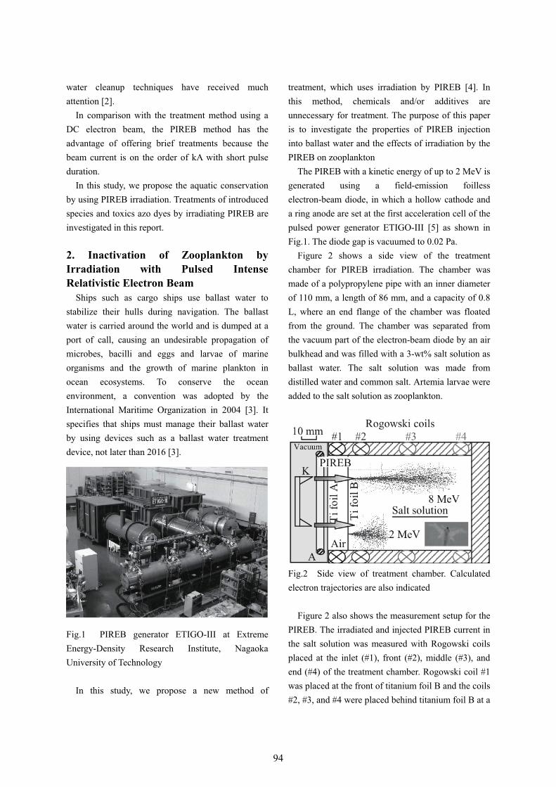
water cleanup techniques have received much attention [2].
In comparison with the treatment method using a DC electron beam, the PIREB method has the advantage of offering brief treatments because the beam current is on the order of kA with short pulse duration.
In this study, we propose the aquatic conservation by using PIREB irradiation. Treatments of introduced species and toxics azo dyes by irradiating PIREB are investigated in this report. 2. Inactivation of Zooplankton by Irradiation with Pulsed Intense Relativistic Electron Beam
Ships such as cargo ships use ballast water to stabilize their hulls during navigation. The ballast water is carried around the world and is dumped at a port of call, causing an undesirable propagation of microbes, bacilli and eggs and larvae of marine organisms and the growth of marine plankton in ocean ecosystems. To conserve the ocean environment, a convention was adopted by the International Maritime Organization in 2004 [3]. It specifies that ships must manage their ballast water by using devices such as a ballast water treatment device, not later than 2016 [3].
Fig.1 PIREB generator ETIGO-III at Extreme Energy-Density Research Institute, Nagaoka University of Technology
In this study, we propose a new method of
treatment, which uses irradiation by PIREB [4]. In this method, chemicals and/or additives are unnecessary for treatment. The purpose of this paper is to investigate the properties of PIREB injection into ballast water and the effects of irradiation by the PIREB on zooplankton
The PIREB with a kinetic energy of up to 2 MeV is generated using a field-emission foilless electron-beam diode, in which a hollow cathode and a ring anode are set at the first acceleration cell of the pulsed power generator ETIGO-III [5] as shown in Fig.1. The diode gap is vacuumed to 0.02 Pa.
Figure 2 shows a side view of the treatment chamber for PIREB irradiation. The chamber was made of a polypropylene pipe with an inner diameter of 110 mm, a length of 86 mm, and a capacity of 0.8 L, where an end flange of the chamber was floated from the ground. The chamber was separated from the vacuum part of the electron-beam diode by an air bulkhead and was filled with a 3-wt% salt solution as ballast water. The salt solution was made from distilled water and common salt. Artemia larvae were added to the salt solution as zooplankton.
Fig.2 Side view of treatment chamber. Calculated electron trajectories are also indicated
Figure 2 also shows the measurement setup for the PIREB. The irradiated and injected PIREB current in the salt solution was measured with Rogowski coils placed at the inlet (#1), front (#2), middle (#3), and end (#4) of the treatment chamber. Rogowski coil #1 was placed at the front of titanium foil B and the coils #2, #3, and #4 were placed behind titanium foil B at a
9494
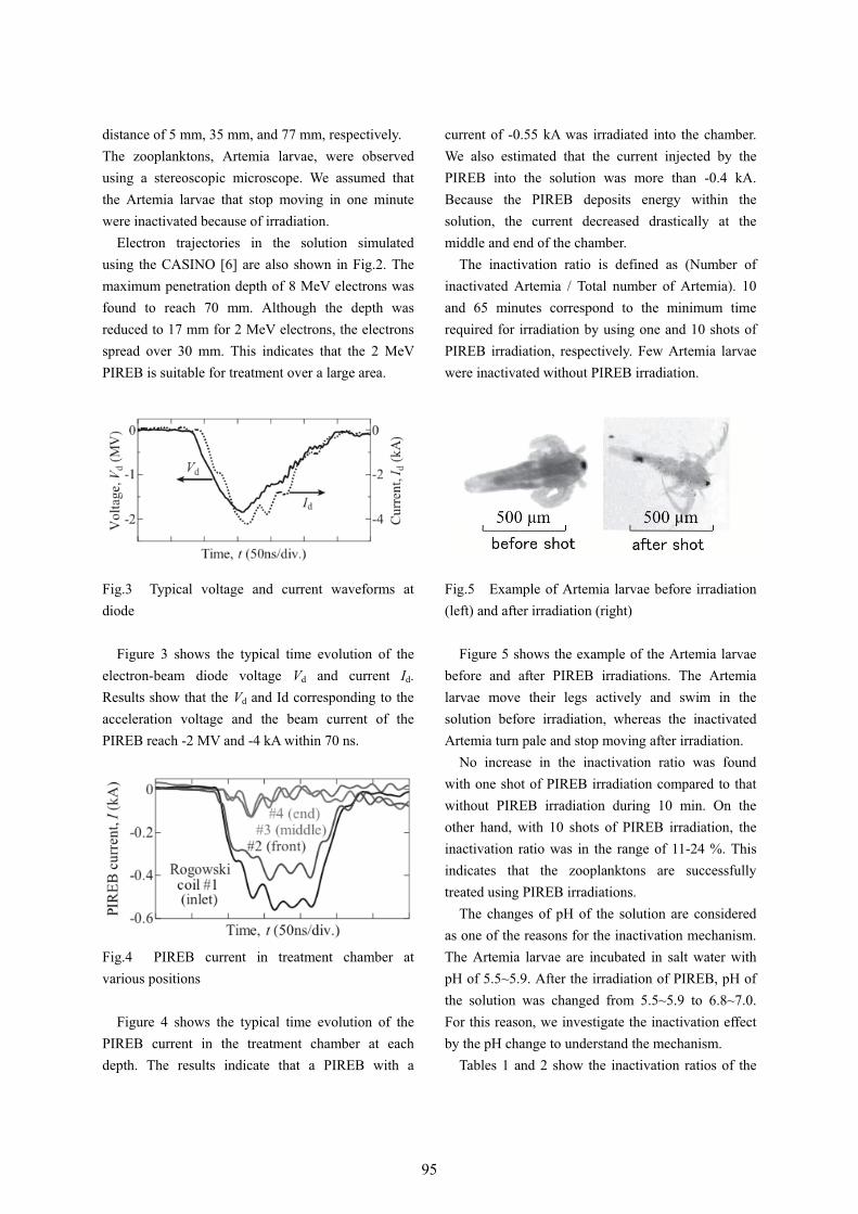
distance of 5 mm, 35 mm, and 77 mm, respectively. The zooplanktons, Artemia larvae, were observed using a stereoscopic microscope. We assumed that the Artemia larvae that stop moving in one minute were inactivated because of irradiation.
Electron trajectories in the solution simulated using the CASINO [6] are also shown in Fig.2. The maximum penetration depth of 8 MeV electrons was found to reach 70 mm. Although the depth was reduced to 17 mm for 2 MeV electrons, the electrons spread over 30 mm. This indicates that the 2 MeV PIREB is suitable for treatment over a large area.
Fig.3 Typical voltage and current waveforms at diode
Figure 3 shows the typical time evolution of the electron-beam diode voltage Vd and current Id. Results show that the Vd and Id corresponding to the acceleration voltage and the beam current of the PIREB reach -2 MV and -4 kA within 70 ns.
Fig.4 PIREB current in treatment chamber at various positions
Figure 4 shows the typical time evolution of the PIREB current in the treatment chamber at each depth. The results indicate that a PIREB with a
current of -0.55 kA was irradiated into the chamber. We also estimated that the current injected by the PIREB into the solution was more than -0.4 kA. Because the PIREB deposits energy within the solution, the current decreased drastically at the middle and end of the chamber.
The inactivation ratio is defined as (Number of inactivated Artemia / Total number of Artemia). 10 and 65 minutes correspond to the minimum time required for irradiation by using one and 10 shots of PIREB irradiation, respectively. Few Artemia larvae were inactivated without PIREB irradiation.
Fig.5 Example of Artemia larvae before irradiation (left) and after irradiation (right)
Figure 5 shows the example of the Artemia larvae before and after PIREB irradiations. The Artemia larvae move their legs actively and swim in the solution before irradiation, whereas the inactivated Artemia turn pale and stop moving after irradiation.
No increase in the inactivation ratio was found with one shot of PIREB irradiation compared to that without PIREB irradiation during 10 min. On the other hand, with 10 shots of PIREB irradiation, the inactivation ratio was in the range of 11-24 %. This indicates that the zooplanktons are successfully treated using PIREB irradiations.
The changes of pH of the solution are considered as one of the reasons for the inactivation mechanism.The Artemia larvae are incubated in salt water with pH of 5.5~5.9. After the irradiation of PIREB, pH of the solution was changed from 5.5~5.9 to 6.8~7.0. For this reason, we investigate the inactivation effect by the pH change to understand the mechanism.
Tables 1 and 2 show the inactivation ratios of the
9595
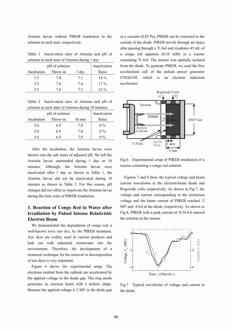
Artemia larvae without PIREB irradiation in the solution at each time, respectively. Table 1 Inactivation ratio of Artemia and pH of solution at each state of Artemia during 1 day
pH of solution InactivationIncubation Throw-in 1 day Ratio
5.5 7.0 7.1 18 % 5.5 7.0 7.4 17 % 5.5 7.0 7.3 23 %
Table 2 Inactivation ratio of Artemia and pH of solution at each state of Artemia during 10 minutes
pH of solution InactivationIncubation Throw-in 10 min Ratio
5.6 6.9 7.0 0 % 5.6 6.9 7.0 0 % 5.6 6.9 7.0 0 %
After the incubation, the Artemia larvae were
thrown into the salt water of adjusted pH. We left the Artemia larvae unattended during 1 day or 10 minutes. Although, the Artemia larvae were inactivated after 1 day as shown in Table 1, the Artemia larvae did not be inactivated during 10 minutes as shown in Table 2. For this reason, pH changes did not affect to inactivate the Artemia larvae during the time scale of PIREB irradiation.
3. Reaction of Congo Red in Water after Irradiation by Pulsed Intense Relativistic Electron Beam
We demonstrated the degradation of congo red, a well-known toxic azo dye, by the PIREB treatment. Azo dyes are widely used in various products and leak out with industrial wastewater into the environment. Therefore, the development of a treatment technique for the removal or decomposition of azo dyes is very important.
Figure 6 shows the experimental setup. The electrons emitted from the cathode are accelerated by the applied voltage in the diode gap. The ring anode generates an electron beam with a hollow shape. Because the applied voltage is 2 MV in the diode gap
in a vacuum (0.02 Pa), PIREB can be extracted to the outside of the diode. PIREB travels through air space after passing through a Ti foil and irradiates 45 mL of a congo red aquation (0.10 mM) in a reactor containing Ti foil. The reactor was spatially isolated from the diode. To generate PIREB, we used the first acceleration cell of the pulsed power generator ETIGO-III, which is an electron induction accelerator.
Fig.6 Experimental setup of PIREB irradiation of a reactor containing a congo red solution
Figures 7 and 8 show the typical voltage and beam current waveforms at the electron-beam diode and Rogowski coils, respectively. As shown in Fig.7, the voltage and current corresponding to the extraction voltage and the beam current of PIREB reached -2 MV and -4 kA at the diode, respectively. As shown in Fig.8, PIREB with a peak current of -0.36 kA entered the solution in the reactor.
Fig.7 Typical waveforms of voltage and current at the diode
9696
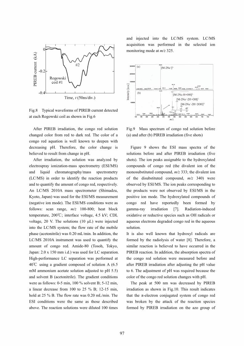
Fig.8 Typical waveforms of PIREB current detected at each Rogowski coil as shown in Fig.6
After PIREB irradiation, the congo red solution changed color from red to dark red. The color of a congo red aquation is well known to deepen with decreasing pH. Therefore, the color change is believed to result from change in pH.
After irradiation, the solution was analyzed by electrospray ionization-mass spectrometry (ESI/MS) and liquid chromatography/mass spectrometry (LC/MS) in order to identify the reaction products and to quantify the amount of congo red, respectively. An LC/MS 2010A mass spectrometer (Shimadzu, Kyoto, Japan) was used for the ESI/MS measurement (negative ion mode). The ESI/MS conditions were as follows: scan range, m/z 100-800; heat block temperature, 200 ; interface voltage, 4.5 kV; CDL voltage, 20 V. The solutions (10 �L) were injected into the LC/MS system; the flow rate of the mobile phase (acetonitrile) was 0.20 mL/min. In addition, the LC/MS 2010A instrument was used to quantify the amount of congo red. Amide-80 (Tosoh, Tokyo, Japan: 2.0 x 150 mm i.d.) was used for LC separation. High-performance LC separation was performed at 40 using a gradient composed of solution A (6.5 mM ammonium acetate solution adjusted to pH 5.5) and solvent B (acetonitrile). The gradient conditions were as follows: 0-5 min, 100 % solvent B; 5-12 min, a linear decrease from 100 to 25 % B; 12-15 min, hold at 25 % B. The flow rate was 0.20 mL/min. The ESI conditions were the same as those described above. The reaction solutions were diluted 100 times
and injected into the LC/MS system. LC/MS acquisition was performed in the selected ion monitoring mode at m/z 325.
Fig.9 Mass spectrum of congo red solution before (a) and after (b) PIREB irradiation (five shots)
Figure 9 shows the ESI mass spectra of the solutions before and after PIREB irradiation (five shots). The ion peaks assignable to the hydroxylated compounds of congo red (the divalent ion of the monosubstituted compound, m/z 333; the divalent ion of the disubstituted compound, m/z 340) were observed by ESI/MS. The ion peaks corresponding to the products were not observed by ESI/MS in the positive ion mode. The hydroxylated compounds of congo red have reportedly been formed by gamma-ray irradiation [7]. Radiation-induced oxidative or reductive species such as OH radicals or aqueous electrons degraded congo red in the aqueous solution. It is also well known that hydroxyl radicals are formed by the radiolysis of water [8]. Therefore, a similar reaction is believed to have occurred in the PIREB reaction. In addition, the absorption spectra of the congo red solution were measured before and after PIREB irradiation after adjusting the pH value to 6. The adjustment of pH was required because the color of the congo red solution changes with pH.
The peak at 500 nm was decreased by PIREB irradiation as shown in Fig.10. This result indicates that the �-electron conjugated system of congo red was broken by the attack of the reaction species formed by PIREB irradiation on the azo group of
9797
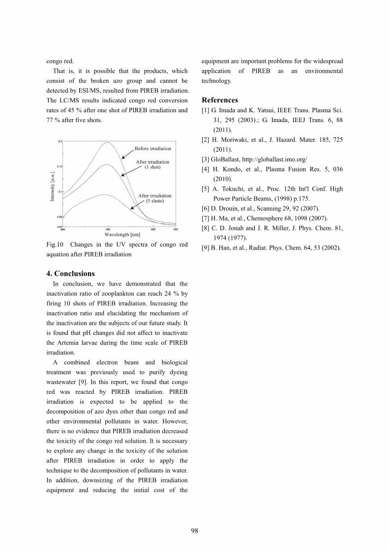
congo red. That is, it is possible that the products, which
consist of the broken azo group and cannot be detected by ESI/MS, resulted from PIREB irradiation. The LC/MS results indicated congo red conversion rates of 45 % after one shot of PIREB irradiation and 77 % after five shots.
Fig.10 Changes in the UV spectra of congo red aquation after PIREB irradiation 4. Conclusions
In conclusion, we have demonstrated that the inactivation ratio of zooplankton can reach 24 % by firing 10 shots of PIREB irradiation. Increasing the inactivation ratio and elucidating the mechanism of the inactivation are the subjects of our future study. It is found that pH changes did not affect to inactivate the Artemia larvae during the time scale of PIREB irradiation.
A combined electron beam and biological treatment was previously used to purify dyeing wastewater [9]. In this report, we found that congo red was reacted by PIREB irradiation. PIREB irradiation is expected to be applied to the decomposition of azo dyes other than congo red and other environmental pollutants in water. However, there is no evidence that PIREB irradiation decreased the toxicity of the congo red solution. It is necessary to explore any change in the toxicity of the solution after PIREB irradiation in order to apply the technique to the decomposition of pollutants in water. In addition, downsizing of the PIREB irradiation equipment and reducing the initial cost of the
equipment are important problems for the widespread application of PIREB as an environmental technology.
References [1] G. Imada and K. Yatsui, IEEE Trans. Plasma Sci.
31, 295 (2003).; G. Imada, IEEJ Trans. 6, 88 (2011).
[2] H. Moriwaki, et al., J. Hazard. Mater. 185, 725 (2011).
[3] GloBallast, http://globallast.imo.org/ [4] H. Kondo, et al., Plasma Fusion Res. 5, 036
(2010). [5] A. Tokuchi, et al., Proc. 12th Int'l Conf. High
Power Particle Beams, (1998) p.175. [6] D. Drouin, et al., Scanning 29, 92 (2007). [7] H. Ma, et al., Chemosphere 68, 1098 (2007). [8] C. D. Jonah and J. R. Miller, J. Phys. Chem. 81,
1974 (1977). [9] B. Han, et al., Radiat. Phys. Chem. 64, 53 (2002).
9898
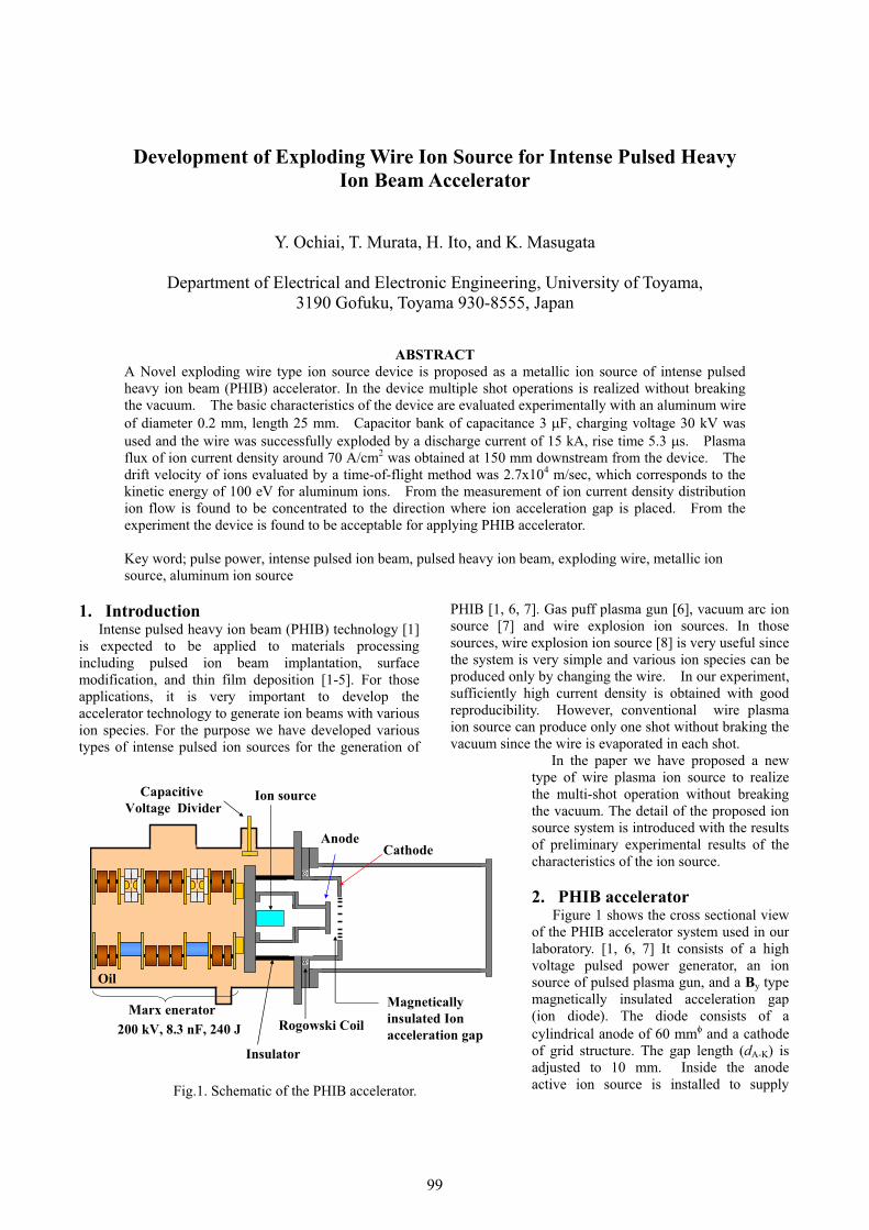
Development of Exploding Wire Ion Source for Intense Pulsed Heavy Ion Beam Accelerator
Y. Ochiai, T. Murata, H. Ito, and K. Masugata
Department of Electrical and Electronic Engineering, University of Toyama, 3190 Gofuku, Toyama 930-8555, Japan
ABSTRACT A Novel exploding wire type ion source device is proposed as a metallic ion source of intense pulsed heavy ion beam (PHIB) accelerator. In the device multiple shot operations is realized without breaking the vacuum. The basic characteristics of the device are evaluated experimentally with an aluminum wire of diameter 0.2 mm, length 25 mm. Capacitor bank of capacitance 3 �F, charging voltage 30 kV was used and the wire was successfully exploded by a discharge current of 15 kA, rise time 5.3 �s. Plasma flux of ion current density around 70 A/cm2 was obtained at 150 mm downstream from the device. The drift velocity of ions evaluated by a time-of-flight method was 2.7x10⁴ m/sec, which corresponds to the kinetic energy of 100 eV for aluminum ions. From the measurement of ion current density distribution ion flow is found to be concentrated to the direction where ion acceleration gap is placed. From the experiment the device is found to be acceptable for applying PHIB accelerator.
Key word; pulse power, intense pulsed ion beam, pulsed heavy ion beam, exploding wire, metallic ion source, aluminum ion source
1. Introduction Intense pulsed heavy ion beam (PHIB) technology [1]
is expected to be applied to materials processing including pulsed ion beam implantation, surface modification, and thin film deposition [1-5]. For those applications, it is very important to develop the accelerator technology to generate ion beams with various ion species. For the purpose we have developed various types of intense pulsed ion sources for the generation of
PHIB [1, 6, 7]. Gas puff plasma gun [6], vacuum arc ion source [7] and wire explosion ion sources. In those sources, wire explosion ion source [8] is very useful since the system is very simple and various ion species can be produced only by changing the wire. In our experiment, sufficiently high current density is obtained with good reproducibility. However, conventional wire plasma ion source can produce only one shot without braking the vacuum since the wire is evaporated in each shot.
In the paper we have proposed a new type of wire plasma ion source to realize the multi-shot operation without breaking the vacuum. The detail of the proposed ion source system is introduced with the results of preliminary experimental results of the characteristics of the ion source.
2. PHIB accelerator Figure 1 shows the cross sectional view
of the PHIB accelerator system used in our laboratory. [1, 6, 7] It consists of a high voltage pulsed power generator, an ion source of pulsed plasma gun, and a By type magnetically insulated acceleration gap (ion diode). The diode consists of a cylindrical anode of 60 mm! and a cathode of grid structure. The gap length (dA-K) is adjusted to 10 mm. Inside the anode active ion source is installed to supply
Oil
Insulator
Marx enerator200 kV, 8.3 nF, 240 J
CapacitiveVoltage Divider
Anode
Magnetically insulated Ion acceleration gap
Cathode
Rogowski Coil
Ion source
Fig.1. Schematic of the PHIB accelerator.
9999
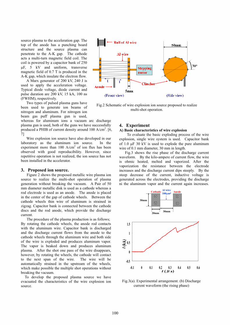
source plasma to the acceleration gap. The top of the anode has a punching board structure and the source plasma can penetrate to the A-K gap. The cathode acts a multi-turn magnetic field coil. The coil is powered by a capacitor bank of 250 �F, 5 kV and uniform, transverse magnetic field of 0.7 T is produced in the A-K gap, which insulate the electron flow.
A Marx generator of 200 kV, 240 J is used to apply the acceleration voltage. Typical diode voltage, diode current and pulse duration are 200 kV, 15 kA, 100 ns (FWHM), respectively.
Two types of pulsed plasma guns have been used to generate ion beams of nitrogen and aluminum. For nitrogen ion beam gas puff plasma gun is used, whereas for aluminum ions a vacuum arc discharge plasma gun is used, both of the guns we have successfully produced a PHIB of current density around 100 A/cm2. [6, 7]
Wire explosion ion source have also developed in our laboratory as the aluminum ion source. In the experiment more than 100 A/cm2 of ion flux has been observed with good reproducibility. However, since repetitive operation is not realized, the ion source has not been installed in the accelerator.
3. Proposed ion source. Figure 2 shows the proposed metallic wire plasma ion source to realize the multi-shot operation of plasma generation without breaking the vacuum. A Pair of 50 mm diameter metallic disk is used as a cathode whereas a rod electrode is used as an anode. The anode is placed in the center of the gap of cathode wheels. Between the cathode wheels thin wire of aluminum is strained in zigzag. Capacitor bank is connected between the cathode discs and the rod anode, which provide the discharge current.
The procedure of the plasma production is as follows; By rotating the cathode wheels, the anode rod contacts with the aluminum wire. Capacitor bank is discharged and the discharge current flows from the anode to the cathode wheels through the aluminum wire and both side of the wire is exploded and produces aluminum vapor. The vapor is beaked down and produces aluminum plasma. After the shot one pass of the wire disappears, however, by rotating the wheels, the cathode will contact to the next span of the wire. The wire will be automatically strained in the upstream of the wheels, which make possible the multiple shot operations without breaking the vacuum.
To develop the proposed plasma source we have evacuated the characteristics of the wire explosion ion source.
4. ExperimentA) Basic characteristics of wire explosion
To evaluate the basic exploding process of the wire explosion, single wire system is used. Capacitor bank of 1.0 �F 30 kV is used to explode the pure aluminum wire of 0.1 mm diameter, 30 mm in length.
Fig.3 shows the rise phase of the discharge current waveform. By the kilo-ampere of current flow, the wire is ohmic heated, melted and vaporized. After the vaporization the resistance between the electrode increases and the discharge current dips steeply. By the steep decrease of the current, inductive voltage is generated across the electrodes, providing the discharge ni the aluminum vapor and the current again increases.
AnodeCathode
20mm
30mm
Al wire 100�m!
30mm
-0.5
0
0.5
1
1.5
-0.1 0 0.1 0.2 0.3 0.4 0.5 0.6
Fig.3(a). Experimental arrangement. (b) Discharge current waveform (the rising phase)
Fig.2 Schematic of wire explosion ion source proposed to realize multi-shot operation.
100100
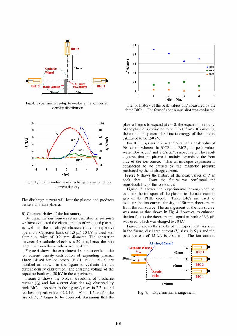
The discharge current will heat the plasma and produces dense aluminum plasma.
B) Characteristics of the ion source By using the ion source system described in section 2 we have evaluated the characteristics of produced plasma, as well as the discharge characteristics in repetitive operation. Capacitor bank of 1.0 �F, 30 kV is used with aluminum wire of 0.2 mm diameter. The separation between the cathode wheels was 20 mm; hence the wire length between the wheels is around 45 mm. Figure 4 shows the experimental setup to evaluate the ion current density distribution of expanding plasma. Three Biased ion collectors (BIC1, BIC2, BIC3) are installed as shown in the figure to evaluate the ion current density distribution. The charging voltage of the capacitor bank was 30 kV in the experiment.
Figure 5 shows the typical waveform of discharge current (Id) and ion current densities (Ji) observed by each BICs. As seen in the figure Id rises in 2.3 �s and reaches the peak value of 8.8 kA. About 1.5 �s after the rise of Id, Ji begin to be observed. Assuming that the
plasma begins to expand at t = 0, the expansion velocity of the plasma is estimated to be 3.3x10⁴ m/s. If assuming the aluminum plasma the kinetic energy of the ions is estimated to be 150 eV.
For BIC1, Ji rises in 2 �s and obtained a peak value of 90 A/cm2, whereas in BIC2 and BIC3, the peak values were 13.6 A/cm2 and 3.6A/cm2, respectively. The result suggests that the plasma is mainly expands to the front side of the ion source. This un-isotropic expansion is considered to be caused by the magnetic pressure produced by the discharge current. Figure 6 shows the history of the peak values of Ji in each shot. From the figure we confirmed the reproducibility of the ion source. Figure 7 shows the experimental arrangement to evaluate the transport of the plasma to the acceleration gap of the PHIB diode. Three BICs are used to evaluate the ion current density at 150 mm downstream from the ion source. The arrangement of the ion source was same as that shown in Fig. 4, however, to enhance the ion flux to the downstream, capacitor bank of 3.3 �Fwas used, which was charged to 30 kV
Figure 8 shows the results of the experiment. As seen in the figure, discharge current (Id) rises in 5 �s and the peak current of 15 kA is obtained. The ion current
50mm
50mm
50mm
Al wire
Cathode Wheel
BIC 1
BIC 2
BIC 3 (0.2 mm!)Rode Anode
50mm
50mm
50mm
Al wire
Cathode Wheel
BIC 1
BIC 2
BIC 3 (0.2 mm!)Rode Anode
Fig.4. Experimental setup to evaluate the ion current density distribution
-2
0
2
4
6
8
10
-1 0 1 2 3 4 5-20
0
20
40
60
80
100
I d(k
A)
J i(A
/cm
2 )
t (�s)
BIC 1
BIC2
BIC 3
Id
-2
0
2
4
6
8
10
-1 0 1 2 3 4 5-20
0
20
40
60
80
100
I d(k
A)
J i(A
/cm
2 )
t (�s)
BIC 1
BIC2
BIC 3
Id
I d(k
A)
J i(A
/cm
2 )
t (�s)
BIC 1
BIC2
BIC 3
Id
Fig.5. Typical waveforms of discharge current and ion current density
150mm
40mm
40mm
20mm
Al wire, 0.2mmf
Anoderode
Cathode Wheels
BIC 1
BIC 2
BIC 3
150mm
40mm
40mm
20mm
Al wire, 0.2mmf
Anoderode
Cathode Wheels
BIC 1
BIC 2
BIC 3
Fig. 7. Experimental arrangement.
0
20
40
60
80
100
0 1 2 3 4 5
BIC1BIC2BIC3J(
A/c
m2 )
Shot No.
0
20
40
60
80
100
0 1 2 3 4 5
BIC1BIC2BIC3J(
A/c
m2 )
Shot No. Fig. 6. History of the peak values of Ji measured by the three BICs. For four of continuous shot was evaluated.
101101
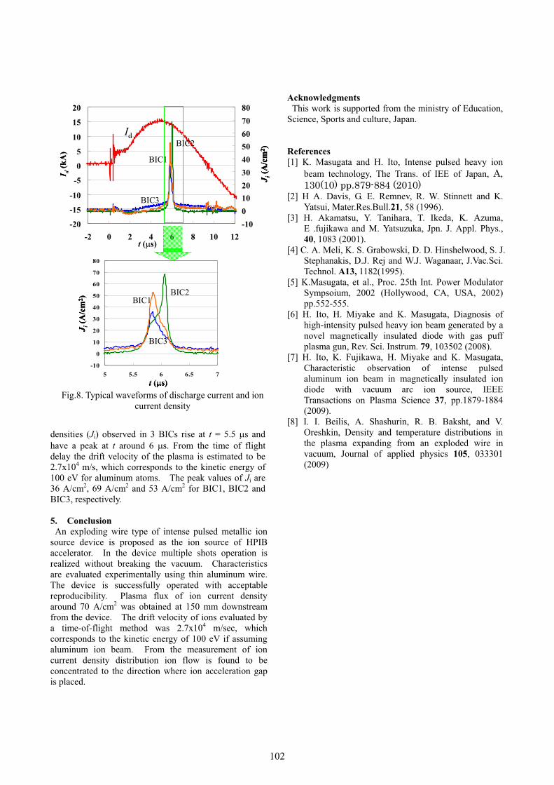
densities (Ji) observed in 3 BICs rise at t = 5.5 �s and have a peak at t around 6 �s. From the time of flight delay the drift velocity of the plasma is estimated to be 2.7x10⁴ m/s, which corresponds to the kinetic energy of 100 eV for aluminum atoms. The peak values of Ji are 36 A/cm2, 69 A/cm2 and 53 A/cm2 for BIC1, BIC2 and BIC3, respectively.
5. Conclusion An exploding wire type of intense pulsed metallic ion
source device is proposed as the ion source of HPIB accelerator. In the device multiple shots operation is realized without breaking the vacuum. Characteristics are evaluated experimentally using thin aluminum wire. The device is successfully operated with acceptable reproducibility. Plasma flux of ion current density around 70 A/cm2 was obtained at 150 mm downstream from the device. The drift velocity of ions evaluated by a time-of-flight method was 2.7x10⁴ m/sec, which corresponds to the kinetic energy of 100 eV if assuming aluminum ion beam. From the measurement of ion current density distribution ion flow is found to be concentrated to the direction where ion acceleration gap is placed.
Acknowledgments This work is supported from the ministry of Education,
Science, Sports and culture, Japan.
References [1] K. Masugata and H. Ito, Intense pulsed heavy ion
beam technology, The Trans. of IEE of Japan, A, 130(10) pp.879-884 (2010)
[2] H A. Davis, G. E. Remnev, R. W. Stinnett and K. Yatsui, Mater.Res.Bull.21, 58 (1996).
[3] H. Akamatsu, Y. Tanihara, T. Ikeda, K. Azuma, E .fujikawa and M. Yatsuzuka, Jpn. J. Appl. Phys., 40, 1083 (2001).
[4] C. A. Meli, K. S. Grabowski, D. D. Hinshelwood, S. J. Stephanakis, D.J. Rej and W.J. Waganaar, J.Vac.Sci. Technol. A13, 1182(1995).
[5] K.Masugata, et al., Proc. 25th Int. Power Modulator Sympsoium, 2002 (Hollywood, CA, USA, 2002) pp.552-555.
[6] H. Ito, H. Miyake and K. Masugata, Diagnosis of high-intensity pulsed heavy ion beam generated by a novel magnetically insulated diode with gas puff plasma gun, Rev. Sci. Instrum. 79, 103502 (2008).
[7] H. Ito, K. Fujikawa, H. Miyake and K. Masugata, Characteristic observation of intense pulsed aluminum ion beam in magnetically insulated ion diode with vacuum arc ion source, IEEE Transactions on Plasma Science 37, pp.1879-1884 (2009).
[8] I. I. Beilis, A. Shashurin, R. B. Baksht, and V. Oreshkin, Density and temperature distributions in the plasma expanding from an exploded wire in vacuum, Journal of applied physics 105, 033301 (2009)
-20
-15
-10
-5
0
5
10
15
20
-2 0 2 4 6 8 10 12-1001020304050607080
t (�s)
I d(k
A)
-10
0
10
20
30
40
50
60
70
80
5 5.5 6 6.5 7
J i(A
/cm
2 )
J i(A
/cm
2 )
t (�s)
Id
BIC1
BIC2
BIC3
BIC2BIC1
BIC3
-20
-15
-10
-5
0
5
10
15
20
-2 0 2 4 6 8 10 12-1001020304050607080
t (�s)
I d(k
A)
-10
0
10
20
30
40
50
60
70
80
5 5.5 6 6.5 7
J i(A
/cm
2 )
J i(A
/cm
2 )
t (�s)
-20
-15
-10
-5
0
5
10
15
20
-2 0 2 4 6 8 10 12-1001020304050607080
t (�s)
I d(k
A)
-10
0
10
20
30
40
50
60
70
80
5 5.5 6 6.5 7
J i(A
/cm
2 )
J i(A
/cm
2 )
t (�s)
Id
BIC1
BIC2
BIC3
BIC2BIC1
BIC3
Fig.8. Typical waveforms of discharge current and ion current density
102102