photon induced electron transfer in quantum dot solar cell
TRANSCRIPT
International Journal of Scientific and Research Publications, Volume 5, Issue 2, February 2015 1 ISSN 2250-3153
www.ijsrp.org
Photon Induced Electron Transfer in Quantum Dot Solar
Cell
Ubani Charles Ahamefula
* Department of Physics, Universiti Kebangsaan Malaysia, Bangi, 43600 Selangor D.E., Malaysia.
Abstract- Low dimensional semiconductor crystals structures otherwise known as quantum dots are in possession of unique
optoelectronic properties that allow the flow of electrons to be harvested instantaneously. The advent of quantum dot for various
technological applications is motivated by their flexibility of their bandgap supporting their capability to tap power from the visible
spectrum as well as the invisible infrared through absorbable wavelength ranges from about 700 nanometre to 10 micron. Besides the
wide energy harvesting range, quantum dot utilizes small to area for high energy production. The emergence of quantum dot and its
application in optoelectronic device such as solar is set to improve the efficiency limit of traditional devices. The configuration of
quantum dot in solar cell is discussed as well as electron transfer processes. Their three unique advantages for solar-to-electric energy
conversion such as provision of large surface and interfacial areas per unit volume for light absorption and charge separation. The
confinement process of charge carriers in quantum dot provides the ability to tune the optical and electronic properties of materials in
ways that are not possible with bulk materials. The study shows that the incorporation of quantum into solar cell could enhance the
performance of devices and as well, low their cost.
Index Terms- Quantum dots, Electron transfer, optoelectronic properties, Charge carriers, Solar cell.
I. INTRODUCTION
he cost of photovoltaic (PV) power is determined by the PV module conversion efficiency as well as the capital cost of the PV
system per unit area. The ratio of the capital cost per unit area (RM/m2) to the peak power (Wp) produced per unit area yields the
generated power cost in the unit of RM/peak watt (RM/Wp). The cost of finite energy sources (gas and petroleum) in 2007 ranges
from 0.25 – 0.35 RM/kWh while PV generated power was in the range of 28 RM/Wp (RM 17.5 for the PV module plus RM 10.5 for
the balance of system cost). Owing to the increase in energy demand, active components for PV cell must be rid of the barriers to high
efficiency such as the avoidance of internal losses due to non-radiative centres and the generation of excessive heat which is
predominant in conventional silicon based solar cells. Presently, the market share of silicon-based solar cells comprises single crystal,
polycrystal, and amorphous silicon is about 99%. Silicon-based solar cell consumes huge amount of energy, requires high temperature
purification of the raw material and many processing steps and as a result, is expensive. “Photon induced charge transfer of quantum
dot in solar cell” is favoured by nano-sized domain energetic semiconductors particles capable of absorbing wide electromagnetic
spectrum and can be structured to avoid premature recombination of electrons-hole pairs.
To meet the global energy demand as well as encouraging wider use of solar power on terawatt scale (TW), there is need to
develop low-cost PV cell with high conversion efficiency. The efficiency of semiconducting material used in solar cell for absorbing
sunlight varies with respect to their energy gap while, the solar spectrum contains photon of wavelength between 700nm to 10 micron
or in terms of energy between 0.5eV to 3.5eV. Absorption of solar photons larger than the bandgap create electron – hole pairs with
the total energy equivalent to the difference between the photogenerated electron energy and the conduction band energy [1–4].
However, in a single-junction solar cell made of semiconductor material such as silicon, spectral losses can be as large as
50%. This is as a result of the mismatch between the incident solar spectrum and the spectral absorption properties of the material [5].
Large part of the solar spectrum is not absorbed as a result of the band gap (Eg) of the material. Photons with energy (Eph) larger than
the band gap are absorbed while the excess energy Eph−Eg is effectively transferred to the electrons as thermal energy. Photons with
Eph < Eg are not absorbed. Alternatively, report [6] on CuInSe2 (CIS) based solar cell is promising though limited by the complexity
and complicated nature of the technology. In search for breakthrough on cost and efficiency, nanocrytalline dye sensitized solar cells
in contrast to Si and CIS cells offer promising functional element for light absorption as well as charge separation. Currently, the
chemisorption of dye on the surface of the semiconductor was developed to enhance the function of the dye [7, 8]. The concept uses
dispersed particles to provide enhanced surface interface [9]. Photoelectrodes having high surface roughness were employed with
TiO2 as the choice semiconductor [10, 11]. The materials are inexpensive, non-toxic and abundant. A conversion efficiency of 7.1 %
was obtained in 1991 [12] while the efficiency to date is over 18 %. In another development, quantum dot solar cells exploit quantum
confinement either to tune the optical absorption spectrum of the solar cell or to generate multiple excitons (MEG). Though this has
not to date been demonstrated in an actual solar cell several proposed designs have been reported [13, 14]. In these designs the dye
molecules are replaced with a layer of quantum dots adsorbed onto nanowires. Such solar cell operates in a similar manner to the dye
T
International Journal of Scientific and Research Publications, Volume 5, Issue 2, February 2015 2
ISSN 2250-3153
www.ijsrp.org
sensitized solar cell but the light would be absorbed by the quantum dots instead of the dye molecules. The concept of quantum dot
sensitized solar cell [15] based on CdSe quantum dots attached to ZnO nanowires was used to demonstrate the absorption of light
energy to generate electrons that were then transferred to the nanowire to create electrical current. Report shows that better utilization
of the solar spectrum takes place in quantum dot sensitized solar cell [16]. Besides its wide energy harvesting range, quantum dot may
be painted onto walls or windows, sprayed on clothing, or printed onto rolls of paper. Owing to the design flexibility of QDSSCs,
handheld devices ranging from PDAs and iPods to cell phones could be powered eliminating need for electrical cords through the use
of QDSSC.
II. QUANTUM DOTS SENSITIZATION SOLAR CELL (QDSSC)
Quantum dot sensitized solar cells (QDSCs) offers an ideal approach to third generation solar cells [17-20]. The intrinsic attractive
properties of quantum dots (QDs) (tunable band gap [21] high extinction coefficients, [21, 22] and large intrinsic dipole moment [23,
24]) is of advantage over metallorganic dyes as alternative light absorbing medium. Couple with the demonstration of MEG by impact
ionization, QDs [25, 26] could extend the thermodynamic efficiency limit of these devices to 44% [18] ignoring 31% of the Schockley
Queisser detailed balance limit. Although the conceptual efficiencies of QDSCs have not been attained [27] QD-sensitized
nanostructured solar cells are rapidly been researched on as a promising alternative to conventional solar cells [28-31]. The principle
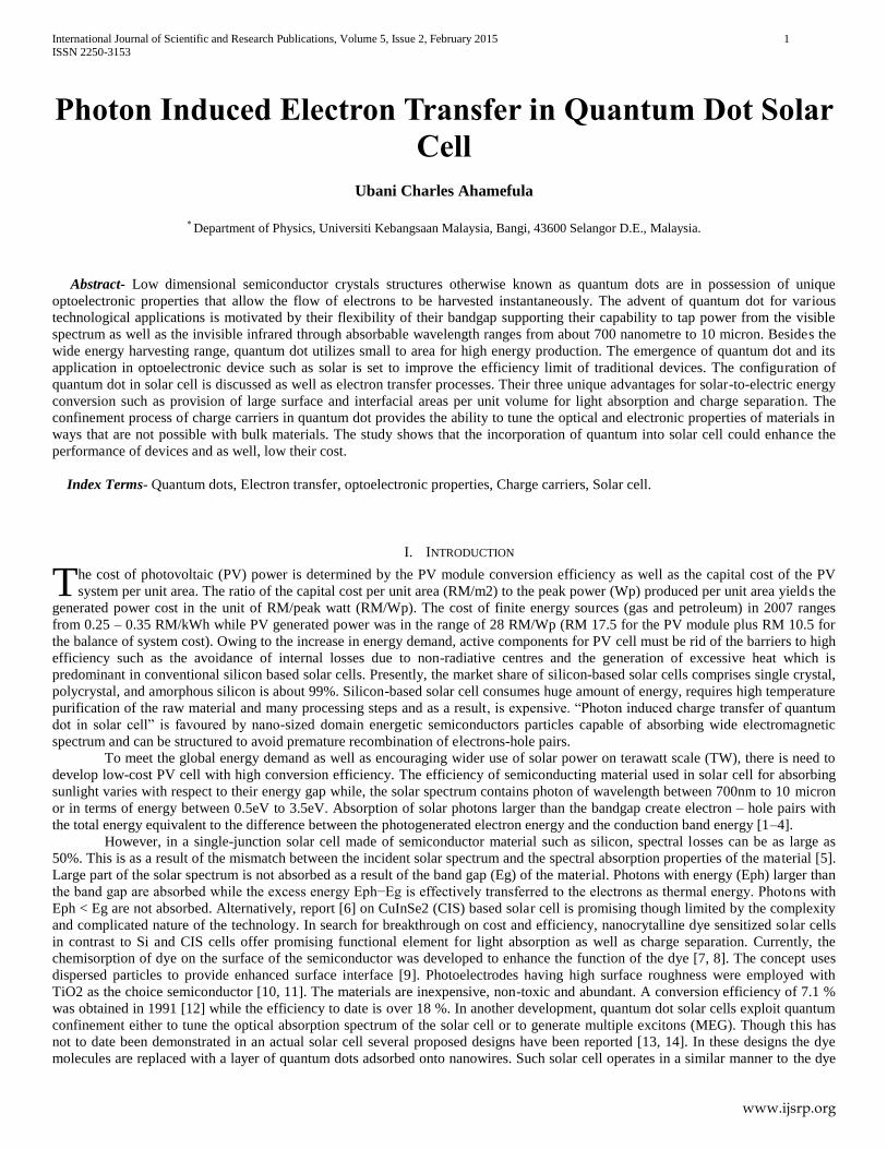
of the sensitized solar cell is explained in Fig. 1.
Fig. 1 Generalised Electron and Hole Orbital and Cell Movement in QDSSCs: (a) Photoexitation of the Light-Absorbing Material; (b)
Electron/Hole Pair Photogeneration; (c) Movement of the Generated Hole from the HOMO of the Light-Absorbing Material to the VB
of the Hole-Conducting Material via the Transfer of an Electron from the Latter to the Former; (d) Electron Flow from the Excited
State of the Light-Absorbing Material to the CB of the Electron Conducting Material; (e) Electron Flow Through the Photoelectrode
and the External Circuit, Re-entering Through the Counter Electrode; (f) Regeneration of the Hole-Conducting Material
In general, sensitized solar cell is made up of three principle components: a light-absorbing material, an electron-conducting
material and a hole-conducting material. A Quantum Dot Sensitized Solar Cell is shown in Fig. 2. In a QDSC, it is the QDs that
absorb the light, creating an electron/hole pair. The efficiency of QDSSCs depends on the spectral absorbance of the QDs
semiconductor material and the electron/hole injection efficiency, the electron transport and recombination rates, which are dependent
on the electron-conducting material; and the hole transport and stability is related to the hole conductor used. The processes taken
place in a QDSSC such as photoexcitation, electron injection as well as recombination of electrons and holes is shown in Fig. 2.
QDSSC are sandwiched between two electrical contacts or electrodes.
International Journal of Scientific and Research Publications, Volume 5, Issue 2, February 2015 3
ISSN 2250-3153
www.ijsrp.org
M
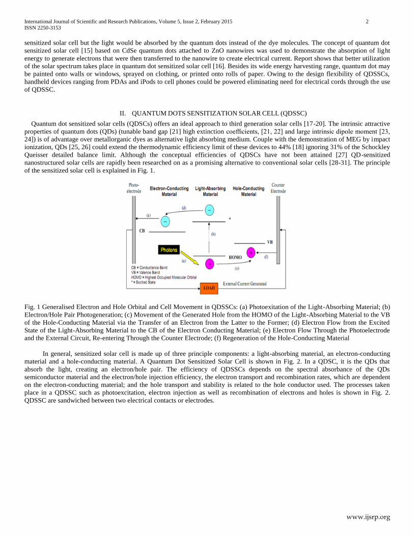
Fig. 2 Diagrammatic representation of electronic band structure of 3.5 nm CdSe with bandgap of 2.17 eV and nanocrystalline TiO2:N
having bandgap of 3.2 eV, in association with TiO2 and a N dopant state of about 1.14 eV above the valence band. Electron and hole
generation, relaxation, and recombination pathways are shown in the figure with (A) photoexcitation of an electron from the valence
band (VB) to the conduction band (CB) of TiO2, (B) transition or photoexcitation of an electron from the N energy level to the CB of
TiO2, (C) recombination of an electron in the CB of TiO2 with a hole in the N energy level, (D) electron transfer or injection from the
CB of a CdSe QD to the CB of TiO2, and (E) hole transfer from the VB of a CdSe QD to the N energy level. Note that not all of these
processes can happen simultaneously, and many of these are competing processes. [76].
On illumination and creation of electron/hole pairs, electrons injected into an electron-conducting material flow through to
the anode and return through the cathode creating an external current which can be used by a load. The electron reduces the oxidised
hole conductor and restores it to its original state as shown in Figure 3.1.
The sensitization of a wide gap nanostructured semiconductor electrode such as TiO2 and ZnO with QDs can be achieved through
either; (1) direct growth of the semiconductor QDs onto the electrode surface by chemical reaction of ionic species using chemical
bath deposition (CBD) [30 - 33] or successive ionic layer adsorption and reaction (SILAR) [34, 35] and (2) through presynthesized
colloidal QDs attached to the electrode material by a bifunctional linker molecule [36-40]. The attachment of colloidal QDs through
molecular wires enhances the morphological properties of the semiconductor nanocrystals. Attaching the QDs onto the TiO2 surface
without molecular linkers is termed direct adsorption (DA) [41]. Higher surface coverage of colloidal QDs on the TiO2 substrate
improves the efficiencies of QDSSCs as well as the network configuration.
III. CONFIGURATION OF QDS IN SOLAR CELL
A. The Sensitizer
The sensitizer on the surface of the nanocrystalline semiconductor absorbs incoming photon flux. To achieve high conversion
efficiencies, the photochemical, electrochemical, and chemical properties of the sensitizer play important role. Owing to the quantum
size effect the edge of the absorption spectra of QD material can be tuned to different sizes. This can be done by varying the
synthesizing temperature. Such an effect produces narrow size distribution [42-45] as absorption occurs throughout the visible region.
To ensure a good injection rate of the photoexcited electron from the sensitizer into the TiO2 a long excited state of the sensitizer is
necessary since injection occurs on the femto-to picosecond time scale. The sensitizer performance determines the output current of
the QDSSC [46]. An illustration showing the generation and flow of electron/hole pairs, through the anode to the cathode is as shown
in Fig. 3. The oxidized hole restores the system to its original state.
For efficient electron injection into the TiO2, the energy level of the sensitizer excited state must be higher than the energy of
the lower edge of the conduction band of the semiconductor as the oxidation potential of the sensitizer excited state increases
negatively than the oxidation potential of the TiO2 semiconductor. On the other hand, the energy level of the oxidized sensitizer has to
be lower than the energy level of the reduced hole-conductor to ensure an efficient regeneration of the sensitizer. For the QD size
distribution, a size limit exists for the nanoparticles to inject electrons into the TiO2 [47].
International Journal of Scientific and Research Publications, Volume 5, Issue 2, February 2015 4
ISSN 2250-3153
www.ijsrp.org
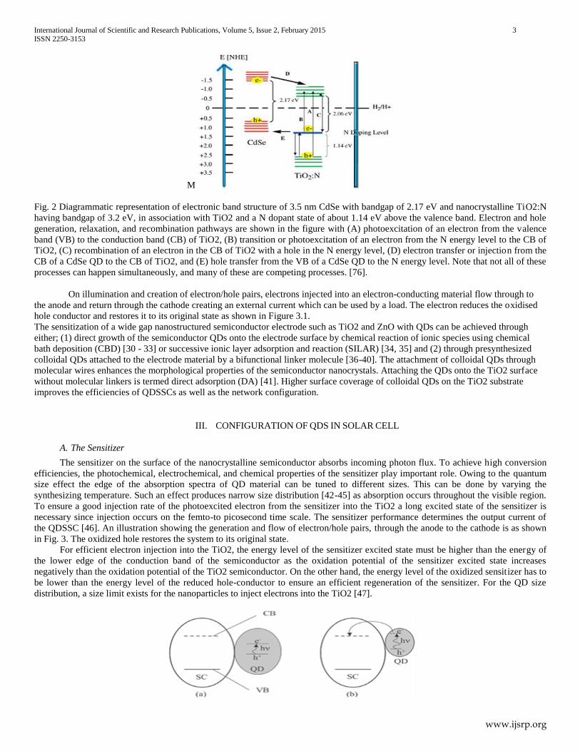
Fig. 3 Electronic levels in semiconductor (SC) and QD particles showing the valence band (VB), conduction band (CB) in (a) Large
CdSe particle, (b) Small CdSe particle
Illustration in (Fig 3.(a) is dominated by large QD particles which is adsorbed onto the semiconductor; its small band gap is
as a result of weak quantum confinement. However, energy of the photogenerated electron in this particle is weaker resulting in poor
injection of electron into the semiconductor to affect the process. However, smaller QD as in Fig. 3. (b) depicted that the energy of the
photogenerated electron is greater than that of the lowest unoccupied molecular orbital (LUMO) of the semiconductor resulting in
rapid electron tunneling to the TiO2 particle. To achieve good adsorption of the sensitizer on the semiconductor, chemical bonds have
to exist between both which however, depend on the synthetic route. For QD grown directly on the surface of the semiconductor the
anchoring is due to bonds appearing between the deposited metal ions and the oxygen atom at the surface. QD may also be formed in
the bulk of the deposition solution before migrating to the surface of the semiconductor. The adsorption of the particle may not be due
to metal/oxygen bonds in this case, as no metal valences are available. For metal selenide QD, there is tendency for a hydrogen bond
to form between the selenide atom and the oxygen at the surface.
B. Electron-Conducting Material
Electrons generated in QDSSCs flow through the conduction band of TiO2 to an electrode. The conduction band energy
electron must be efficient for electronic coupling with the sensitizer energy levels and charge separation to minimize the recombining
of the electron with the sensitizer. An electron-conductor with low level of recombination and good electrical connectivity to the
electrode/substrate is preferred. [48] A situation where the injection is greater than the rate of recombination is termed kinetic
redundancy. [49] The kinetic redundancy can be modified by changing the sensitizer-electron-conductor linker groups. [49] Usually
anatase and rutile are used as the linkers. Anatase is preferred to rutile because it is transparent, colourless and stable at low-
temperature. [50] Besides, it has a better light scattering property when compared to rutile, and its efficiency is higher by a factor of
five. [51]
The success of QDSSCs has been partly attributed to the fast electron injection from the QDs to the TiO2 and a slower reversal
process [52]. High speed electron injection is consistent with near 100 % quantum efficiency [51]. Alternative wide band gap
materials such as ZnO [53, 48, 54, 55, 56], Nb2O5 [53, 57], SnO2 [53] and In2O3 [53] are insensitive to the visible spectrum and
absorb high energy UV wavelengths. Such qualities are desirable as they imply strong chemical bonds, stable material [58] and are
transparent to visible light as a result and are therefore more efficient at creating stable electron/hole pairs.
C. Photoelectrode
The type of electrodes use in QDSSCs affects the overall cell performance and marketability of a solar cell. Pt-free counter-electrodes
use in QDSSCs with Au and Cu2S electrodes are expensive [59, 60]. However, carbon electrode has emerge as a better alternative to
Pt electrode owing to their low cost, high electric conductivity, heat resistance and corrosion-inert. Activated carbon-based electrode
assembles onto CdS QDSSCs yielded conversion efficiency of 1.47%. [61]. Photoelectrode fabricated by sequential assembly of CdS
and CdSe QDs can effectively be adsorbed on ZnO nanowire array. The electrodes with nanospheroidal morphology have shown
better performance compared to P25 nanoparticle electrodes owing to their connectivity among nanospheroidal TiO2 particles and
deeper penetration of the electrolyte in QDSSC [62].
D. The Photoelectrode-Anode
The anode is the electron-conducting electrode termed photoelectrode as it is the illuminated electrode. Electron-conducting
materials are usually placed onto the anode to maximize contact by doctor blading, [63, 53, 64-66] screen printing, [63, 67, 50, 64,
68], spin coating, [69] or sol-gel deposition of dissolved electron-conducting material with a binder.[63, 70] The contact and electron-
conducting material could be fired in air to about 450ºC to 500ºC in a case where TiO2 is used to aid the removal of the binder and
solvent [71] as well as sintering the electron-conducting particles to the substrate. [50, 72, 73].
E. The Counter Electrode (Cathode)
Interaction between the hole conductor and the anode results in recombination [74]. The interaction at the cathode must be
fast to be kinetically favourable. Base on this reason, the cathode for instance, (usually ITO glass) is often coated with carbon [75],
platinum [53, 73, 48, 54] or gold. [67, 65, 69]. Poly (3,4-ethylenedioxythiophene) (PEDOT) coated Fx•SnO2 glass could be used as
counter electrode in TiO2 QDSSCs. [74]. In addition, coating the back electrode of QDSSCs with platinum could improve cell
performance. [51] The cathode can as well be adjusted to accommodate equilibrium potential close to the hole conductor’s, as the
anode (the photoelectrode) is predominantly far from the equilibrium potential. Such coating would not be necessary for cells without
iodide/triiodide based hole conductors. Electron transport in nanoparticle QDSSCs such as in TiO2 occur either between the counter
electrode and the working electrode by hopping [75] or through extended diffusion states [48]. Owing to the high electrons mobility in
International Journal of Scientific and Research Publications, Volume 5, Issue 2, February 2015 5
ISSN 2250-3153
www.ijsrp.org
nanoparticle, the disorder of the nanoparticle slows down the electron transport. Electron hopping in the nanoparticle network is
efficient. Electron transport and recombination are interconnected in such a manner that any increase in the transport rate increases the
recombination rate as well; keeping the QDSSC performance stable.[76] The ZnO nanowires with electron diffusivity of 0.05 to 0.5
cm2s-1 could be an alternative to TiO2 nanoparticle. ZnO nanoparticle provide direct path from photogeneration to conducting
substrate and improve electron transport irrespective of its current densities which is the same with TiO2 nanoparticle [77]. Every
electron injected is connected to the substrate [78] as the coiled wires carry the injected electron to the anode. [48]
F. Electrolyte
Electrolytes in QDSSC contain the electrically conductive charges. The electrochemical potential of the interface between a
semiconductor electrode and an electrolyte solution must be the same for the two phases to be in equilibrium. The excess of charge on
the semiconductor due to low density of charge carriers could extend for 10-100 nm into the electrode and forms the space charge
region. The space charge region is associated with positive charge. A p-type semiconductor usually has a Fermi level that is lower
than the redox potential of the electrolyte and as a result, electron flows from the solution to the electrode to generate negatively
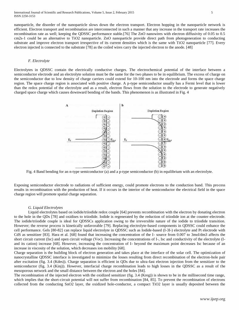
charged space charge which causes downward bending of the bands. This phenomenon is as illustrated in Fig. 4
Fig. 4 Band bending for an n-type semiconductor (a) and a p-type semiconductor (b) in equilibrium with an electrolyte.
Exposing semiconductor electrode to radiations of sufficient energy, could promote electrons to the conduction band. This process
results in recombination with the production of heat. If it occurs in the interior of the semiconductor the electrical field in the space
charge region will promote spatial charge separation.
G. Liquid Electrolytes
Liquid electrolytes based on iodide/triiodide redox couple [64] prevents recombination with the electron by donating electron
to the hole in the QDs [78] and oxidises to triiodide. Iodide is regenerated by the reduction of triiodide ion at the counter-electrode.
The iodide/triiodide couple is ideal for QDSSCs application owing to the irreversible nature of the iodide to triiodide transition.
However; the reverse process is kinetically unfavorable [79]. Replacing electrolyte-based components in QDSSC could enhance the
cell performance. Gels [80-82] can replace liquid electrolyte in QDSSC such as Iodide-based (I-3I-) electrolyte and Pt electrode with
CdS as sensitizer [83]. Hara et al. [68] found that increasing the concentration of the I- source from 0.007 to 3mol/dm3 affects the
short circuit current (Isc) and open circuit voltage (Voc). Increasing the concentrations of I-, Isc and conductivity of the electrolyte (I-
and its cation) increase [68]. However, increasing the concentration of I- beyond the maximum point decreases Isc because of an
increase in viscosity of the solution, which decreases ion mobility [68].
Charge separation is the building block of electron generation and takes place at the interface of the solar cell. The optimization of
nanocrystalline QDSSC interface is investigated to minimize the losses resulting from direct recombination of the electron-hole pair
after excitation (fig. 3.4 (Kdes)). Charge separation is efficient in QDs due to ultra-fast electron injection from the sensitizer to the
semiconductor (fig. 3.4 (Kinj)). However, interfacial charge recombination leads to high losses in the QDSSC as a result of the
mesoporous network and the small distance between the electron and the holes [84].
The recombination of the injected electron with the oxidized sensitizer (fig. 3.4 (Kreg)) is shown to be in the millisecond time range,
which implies that the short-circuit potential will not suffer from recombination [84, 85]. To prevent the recombination of electrons
collected from the conducting SnO2 layer, the oxidized hole-conductor, a compact TiO2 layer is usually deposited between the
International Journal of Scientific and Research Publications, Volume 5, Issue 2, February 2015 6
ISSN 2250-3153
www.ijsrp.org
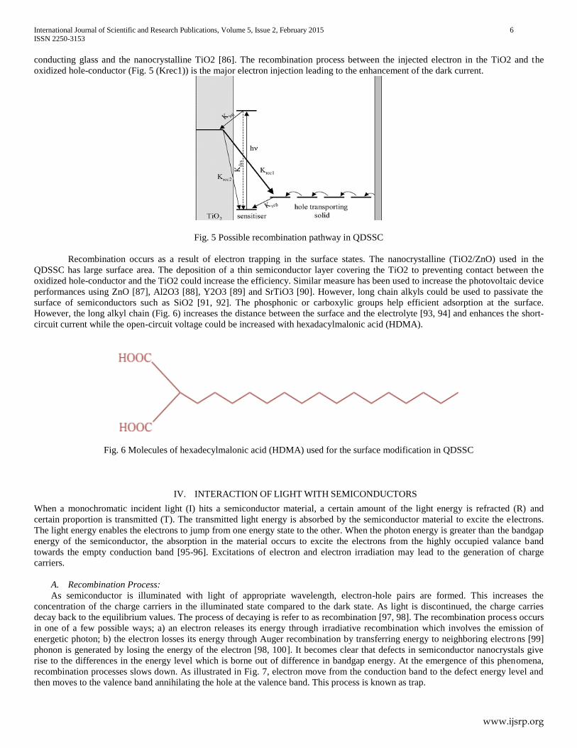
conducting glass and the nanocrystalline TiO2 [86]. The recombination process between the injected electron in the TiO2 and the
oxidized hole-conductor (Fig. 5 (Krec1)) is the major electron injection leading to the enhancement of the dark current.
Fig. 5 Possible recombination pathway in QDSSC
Recombination occurs as a result of electron trapping in the surface states. The nanocrystalline (TiO2/ZnO) used in the
QDSSC has large surface area. The deposition of a thin semiconductor layer covering the TiO2 to preventing contact between the
oxidized hole-conductor and the TiO2 could increase the efficiency. Similar measure has been used to increase the photovoltaic device
performances using ZnO [87], Al2O3 [88], Y2O3 [89] and SrTiO3 [90]. However, long chain alkyls could be used to passivate the
surface of semiconductors such as SiO2 [91, 92]. The phosphonic or carboxylic groups help efficient adsorption at the surface.
However, the long alkyl chain (Fig. 6) increases the distance between the surface and the electrolyte [93, 94] and enhances the short-
circuit current while the open-circuit voltage could be increased with hexadacylmalonic acid (HDMA).
Fig. 6 Molecules of hexadecylmalonic acid (HDMA) used for the surface modification in QDSSC
IV. INTERACTION OF LIGHT WITH SEMICONDUCTORS
When a monochromatic incident light (I) hits a semiconductor material, a certain amount of the light energy is refracted (R) and
certain proportion is transmitted (T). The transmitted light energy is absorbed by the semiconductor material to excite the electrons.
The light energy enables the electrons to jump from one energy state to the other. When the photon energy is greater than the bandgap
energy of the semiconductor, the absorption in the material occurs to excite the electrons from the highly occupied valance band
towards the empty conduction band [95-96]. Excitations of electron and electron irradiation may lead to the generation of charge
carriers.
A. Recombination Process:
As semiconductor is illuminated with light of appropriate wavelength, electron-hole pairs are formed. This increases the
concentration of the charge carriers in the illuminated state compared to the dark state. As light is discontinued, the charge carries
decay back to the equilibrium values. The process of decaying is refer to as recombination [97, 98]. The recombination process occurs
in one of a few possible ways; a) an electron releases its energy through irradiative recombination which involves the emission of
energetic photon; b) the electron losses its energy through Auger recombination by transferring energy to neighboring electrons [99]
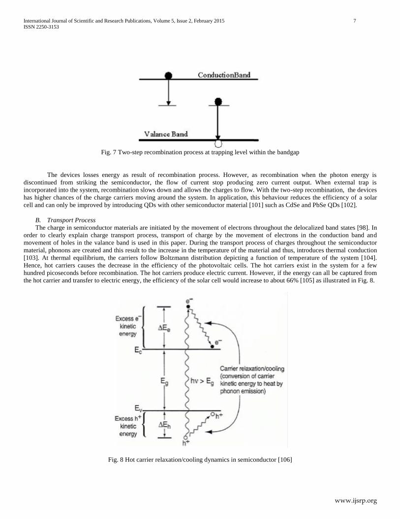
phonon is generated by losing the energy of the electron [98, 100]. It becomes clear that defects in semiconductor nanocrystals give
rise to the differences in the energy level which is borne out of difference in bandgap energy. At the emergence of this phenomena,
recombination processes slows down. As illustrated in Fig. 7, electron move from the conduction band to the defect energy level and
then moves to the valence band annihilating the hole at the valence band. This process is known as trap.
International Journal of Scientific and Research Publications, Volume 5, Issue 2, February 2015 7
ISSN 2250-3153
www.ijsrp.org
Fig. 7 Two-step recombination process at trapping level within the bandgap
The devices losses energy as result of recombination process. However, as recombination when the photon energy is
discontinued from striking the semiconductor, the flow of current stop producing zero current output. When external trap is
incorporated into the system, recombination slows down and allows the charges to flow. With the two-step recombination, the devices
has higher chances of the charge carriers moving around the system. In application, this behaviour reduces the efficiency of a solar
cell and can only be improved by introducing QDs with other semiconductor material [101] such as CdSe and PbSe QDs [102].
B. Transport Process
The charge in semiconductor materials are initiated by the movement of electrons throughout the delocalized band states [98]. In
order to clearly explain charge transport process, transport of charge by the movement of electrons in the conduction band and
movement of holes in the valance band is used in this paper. During the transport process of charges throughout the semiconductor
material, phonons are created and this result to the increase in the temperature of the material and thus, introduces thermal conduction
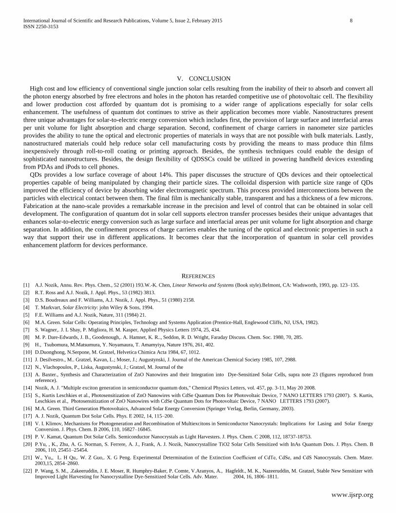
[103]. At thermal equilibrium, the carriers follow Boltzmann distribution depicting a function of temperature of the system [104].
Hence, hot carriers causes the decrease in the efficiency of the photovoltaic cells. The hot carriers exist in the system for a few
hundred picoseconds before recombination. The hot carriers produce electric current. However, if the energy can all be captured from
the hot carrier and transfer to electric energy, the efficiency of the solar cell would increase to about 66% [105] as illustrated in Fig. 8.
Fig. 8 Hot carrier relaxation/cooling dynamics in semiconductor [106]
International Journal of Scientific and Research Publications, Volume 5, Issue 2, February 2015 8
ISSN 2250-3153
www.ijsrp.org
V. CONCLUSION
High cost and low efficiency of conventional single junction solar cells resulting from the inability of their to absorb and convert all
the photon energy absorbed by free electrons and holes in the photon has retarded competitive use of photovoltaic cell. The flexibility
and lower production cost afforded by quantum dot is promising to a wider range of applications especially for solar cells
enhancement. The usefulness of quantum dot continues to strive as their application becomes more viable. Nanostructures present
three unique advantages for solar-to-electric energy conversion which includes first, the provision of large surface and interfacial areas
per unit volume for light absorption and charge separation. Second, confinement of charge carriers in nanometer size particles
provides the ability to tune the optical and electronic properties of materials in ways that are not possible with bulk materials. Lastly,
nanostructured materials could help reduce solar cell manufacturing costs by providing the means to mass produce thin films
inexpensively through roll-to-roll coating or printing approach. Besides, the synthesis techniques could enable the design of
sophisticated nanostructures. Besides, the design flexibility of QDSSCs could be utilized in powering handheld devices extending
from PDAs and iPods to cell phones.
QDs provides a low surface coverage of about 14%. This paper discusses the structure of QDs devices and their optoelectical
properties capable of being manipulated by changing their particle sizes. The colloidal dispersion with particle size range of QDs
improved the efficiency of device by absorbing wider electromagnetic spectrum. This process provided interconnections between the
particles with electrical contact between them. The final film is mechanically stable, transparent and has a thickness of a few microns.
Fabrication at the nano-scale provides a remarkable increase in the precision and level of control that can be obtained in solar cell
development. The configuration of quantum dot in solar cell supports electron transfer processes besides their unique advantages that
enhances solar-to-electric energy conversion such as large surface and interfacial areas per unit volume for light absorption and charge
separation. In addition, the confinement process of charge carriers enables the tuning of the optical and electronic properties in such a
way that support their use in different applications. It becomes clear that the incorporation of quantum in solar cell provides
enhancement platform for devices performance.
REFERENCES
[1] A.J. Nozik, Annu. Rev. Phys. Chem., 52 (2001) 193.W.-K. Chen, Linear Networks and Systems (Book style).Belmont, CA: Wadsworth, 1993, pp. 123–135.
[2] R.T. Ross and A.J. Nozik, J. Appl. Phys., 53 (1982) 3813.
[3] D.S. Boudreaux and F. Williams, A.J. Nozik, J. Appl. Phys., 51 (1980) 2158.
[4] T. Markvart, Solar Electricity: john Wiley & Sons, 1994.
[5] F.E. Williams and A.J. Nozik, Nature, 311 (1984) 21.
[6] M.A. Green. Solar Cells: Operating Principles, Technology and Systems Application (Prentice-Hall, Englewood Cliffs, NJ, USA, 1982).
[7] S. Wagner,. J. L Shay, P. Migliora, H. M. Kasper, Applied Physics Letters 1974, 25, 434.
[8] M. P. Dare-Edwards, J. B., Goodenough,. A. Hamnet, K. R.., Seddon, R. D. Wright, Faraday Discuss. Chem. Soc. 1980, 70, 285.
[9] H., Tsubomura, M.Matsumura, Y. Noyamaura, T. Amamyiya, Nature 1976, 261, 402.
[10] D.Duonghong, N.Serpone, M. Gratzel, Helvetica Chimica Acta 1984, 67, 1012.
[11] J. Desilvestro., M.. Gratzel, Kavan, L.; Moser, J.; Augustynski, J. Journal of the American Chemical Society 1985, 107, 2988.
[12] N., Vlachopoulos, P., Liska, Augustynski, J.; Gratzel, M. Journal of the
[13] A. Baxter., Synthesis and Characterization of ZnO Nanowires and their Integration into Dye-Sensitized Solar Cells, supra note 23 (figures reproduced from reference).
[14] Nozik, A. J. "Multiple exciton generation in semiconductor quantum dots," Chemical Physics Letters, vol. 457, pp. 3-11, May 20 2008.
[15] S., Kurtis Leschkies et al., Photosensitization of ZnO Nanowires with CdSe Quantum Dots for Photovoltaic Device, 7 NANO LETTERS 1793 (2007). S. Kurtis, Leschkies et al., Photosensitization of ZnO Nanowires with CdSe Quantum Dots for Photovoltaic Device, 7 NANO LETTERS 1793 (2007).
[16] M.A. Green. Third Generation Photovoltaics, Advanced Solar Energy Conversion (Springer Verlag, Berlin, Germany, 2003).
[17] A. J. Nozik, Quantum Dot Solar Cells. Phys. E 2002, 14, 115–200.
[18] V. I. Klimov, Mechanisms for Photogeneration and Recombination of Multiexcitons in Semiconductor Nanocrystals: Implications for Lasing and Solar Energy Conversion. J. Phys. Chem. B 2006, 110, 16827–16845.
[19] P. V. Kamat, Quantum Dot Solar Cells. Semiconductor Nanocrystals as Light Harvesters. J. Phys. Chem. C 2008, 112, 18737-18753.
[20] P.Yu, , K., Zhu, A. G. Norman, S. Ferrere, A. J., Frank, A. J. Nozik, Nanocrystalline TiO2 Solar Cells Sensitized with InAs Quantum Dots. J. Phys. Chem. B 2006, 110, 25451–25454.
[21] W., Yu,, L. H Qu,. W. Z Guo,. X. G Peng. Experimental Determination of the Extinction Coefficient of CdTe, CdSe, and CdS Nanocrystals. Chem. Mater. 2003,15, 2854–2860.
[22] P. Wang, S. M., .Zakeeruddin, J. E. Moser, R. Humphry-Baker, P. Comte, V.Aranyos, A., Hagfeldt., M. K., Nazeeruddin, M. Gratzel, Stable New Sensitizer with Improved Light Harvesting for Nanocrystalline Dye-Sensitized Solar Cells. Adv. Mater. 2004, 16, 1806–1811.
International Journal of Scientific and Research Publications, Volume 5, Issue 2, February 2015 9
ISSN 2250-3153
www.ijsrp.org
[23] R., Vogel, K Pohl,. H. Weller, Sensitization of Highly Porous, Polycrystalline TiO2 Electrodes by Quantum Sized CdS. Chem. Phys. Lett. 1990, 174, 241–246.
[24] R.., Vogel, P., Hoyer, H. Weller, Quantum-Sized PdS, CdS, Ag2S, Sb2S3 and Bi2S3 Particles as Sensitizers for Various Nanoporous Wide-Bandgap Semiconductors. J. Phys. Chem. 1994, 98, 3183–3188.
[25] R. D., Schaller, Sykora, M.; Pietryga, J. M.; Klimov, V. I. Seven Excitons at Cost of One: Redefining the Limits for Conversion Efficiency of Photons into Charge Carriers. Nano Lett. 2006, 6, 424–429.
[26] M. T., Trinh, A. J., Houtepen,. J. M.;, Schins, T., Hanrath, J. Piris, W. Knulst, A. P. L. M., Goossens, L. D. A., Siebbeles. In Spite of Recent Doubts Carrier Multiplication Does Occur in PbSe Nanocrystals. Nano Lett. 2008, 8, 1713–1718.
[27] B., O’ReganGra ¨ tzel, M. A Low-Cost High-Efficiency Solar Cell Based on Dye-Sensitized Colloidal TiO2 Films. Nature 1991, 353, 737–740.
[28] O., NiitsooSarkar, S. K.; Pejoux, C.; Ru ¨ hle, S.; Cahen, D.; Hodes, G. Chemical Bath Deposited CdS/CdSe-Sensitized Porous TiO2 Solar Cells. J. Photochem. Photobiol. A 2006, 181, 306–311.
[29] L. J., Diguna, Q., Shen, J., Kobayashi, T. Toyoda, High Efficiency of CdSe Quantum-Dot-Sensitized TiO2 Inverse Opal Solar Cells. Appl. Phys. Lett. 2007, 91, 023116.
[30] H. J., Lee, J. H., Yum, H. C., Leventis, S. M., Zakeeruddin, S. A., Haque, P., Chen, S. I., Seok, Gra ¨ tzel, M.; Nazeeruddin, M. K. CdSe Quantum Dot-Sensitized Solar Cells Exceeding Efficiency 1% at Full-Sun Intensity. J. Phys. Chem. C 2008, 112, 11600–11608.
[31] Y., Diamant, S. G., Chen, O., Melamed, A., Zaban, Core-Shell Nanoporous Electrode for Dye Senxitized Solar Cells: the Effect of the SrTiO3 Shell on the Electronic Properties of the TiO2 Core. J. Phys. Chem. B 2003, 107, 1977–1981.
[32] S., Gime ´ nez, Mora-Sero ´ , I. Macor, L.; Guijarro, N.; T, Lana-Villarreal, R. Go ´mezL. J. Diguna, Q., Shen, T., Toyoda, J. Bisquert, Improving the Performance of Colloidal Quantum-Dot-Sensitized Solar Cells. Nanotechnology 2009, 20, 295204.
[33] Y. F. Nicolau, Solution Deposition of Thin Solid Compound Films by a Successive Ionic-Layer Adsorption and Reaction Process. Appl. Surf. Sci. 1985, 22 3, 1061–1074.
[34] Y. F., Nicolau, M., Dupuy, M., Brunel, ZnS, CdS, and Zn1-XCdXS Thin-Film Deposited by the Successive Ionic Layer Adsorption and Reaction Process. J. Electrochem. Soc. 1990, 137, 2915–2924.
[35] I.., Robel, V., Subramanian, M., Kuno, P. V. Kamat, Quantum Dot Solar Cells. Harvesting Light Energy with CdSe Nanocrystals Molecularly Linked to Mesoscopic TiO2 Films. J. Am. Chem. Soc. 2006, 128, 2385–2393.
[36] T. Lo ´ pez-Luque, A., Wolcott, L. P., Xu, S., Chen, Z., Wen, J., Li, De la, E., Rosa, J. Z., Zhang, Nitrogen-Doped and CdSe Quantum-Dot-Sensitized Nanocrystalline TiO2 Films for Solar Energy Conversion Applications. J. Phys. Chem. C 2008, 112, 1282–1292.
[37] S. K., Leschkies, R., Divakar, J., Basu, E., Enache-Pommer, J. E., Boercker, C. B Carter., U. R.., Kortshagen, , D. J., Norris Aydil, E. S. Photosensitization of ZnO Nanowires with CdSe Quantum Dots for Photovoltaic Devices. Nano Lett. 2007, 7, 1793–1798.
[38] I.., Mora-Sero ´ , S., Gime ´ nez, T., F.; Moehl, Fabregat-Santiago, T., Lana-Villareal, R., J. Go ´mez, Bisquert, Factors Determining the Photovoltaic Performance of a CdSe Quantum Dot Sensitized Solar Cell: The P. V. Role of the Linker Molecule and of the Counter Electrode. Nanotechnology 2008, 19, 424007.
[39] A., Kongkanand, K., Tvrdy, K.., M., Takechi, Kuno, Kamat, Quantum Dot Solar Cells. Tuning Photoresponse throughSize and Shape Control of CdSe TiO2 Architecture. J. Am. Chem. Soc. 2008, 130, 4007–4015.
[40] N., Guijarro, T., Lana-Villarreal, , I., Mora-Sero ´ , J. BisquertGo ´mez, R. CdSe Quantum Dot Sensitized TiO2 Electrodes:Effect of QD Coverage and Mode of Attachment. J. Phys. Chem. C 2009, 113, 4208–4214.
[41] S., Gorer, G. Hodes,. Quantum-Size Effects in the Study of Chemical Solution Deposition Mechanims of Semiconductor Films.J. Phys. Chem. 1994, 98, 5338–5346.
[42] S., Gorer, G., Hodes, Studies in Surface Science and catalysis 1996, 103, 297.
[43] S.; Gorer, G., Hodes, Journal of Physical Chemistry 1994, 98, 5338.
[44] H., Weller, Adv. Mater. 1993, 5.
[45] R., Vogel, P., Hoyer, H., Weller, J. Phys. Chem. 1994, 98, 3183.
[46] G., Hodes, Comparison of Dye- and Semiconductor-Sensitized Porous Nanocrystalline Liquid Junction Solar Cells. J. Phys. Chem. C 2008, 112, 17778–17787.
[47] A. Henglein, Ber. Bunsenges. Phys. Chem. 1995, 99, 903.
[48] J. B. Baxter, E. S. Aydil, Sol. Energy Mater. Sol. Cells 2006, 90, 607.
[49] N. Robertson, Angew. Chem. Int. Ed. 2006, 45, 2338.
[50] G. E. Tulloch, J. Photochem. Photobiol., A 2004, 164, 209.
[51] S. Deb, K, Sol. Energy Mater. Sol. Cells 2005, 88, 1.
[52] R. J. Ellingson, J. B. Asbury, S. Ferrere, A. N. Ghosh, T. Lian, A. J. Nozik, Phys. Chem. 1999, 212 77
[53] K. Hara, T. Horiguchi, T. Kinoshita, K. Sayama, H. Sugihara, H. Arakawa, Sol. Energy Mater. Sol. Cells 2000, 64, 115.
[54] D. C. Olson, J. Pirisa, R. T. Collinsb, S. E. Shaheena, D. S. Ginleya, Thin Solid Films 2006, 496, 26. .
[55] K. Tennakone, G. R. R. Kumara, I. R. M. Kottegoda, V. S. P. Perera, Chem. Commun. 1998, 10, 3825.
[56] T. Oekermann, T. Yoshidaa, H. Tadac, H. Minour, Thin Solid Films 2006, 511-512, 354.
[57] K. Sayama, H. Suguhara, H. Arakawa, Chem. Mater. 1998, 10, 3825.
[58] M. Graetzel, Nature 2001, 414, 338.
[59] Y.-L. Lee, Y.-S. Lo, Adv. Funct. Mater. 19 (2009) 604.
[60] S. Giménez, I. Mora-Seró, L. Macor, N. Guijarro, T. Lana-Villarreal, R. Gómez, L.J. Diguna, Q. Shen, T. Toyoda, J. Bisquert, Nanotechnology 20 (2009) 295204.
[61] J. Seo, W. J. Kim, S. J. Kim, K. Lee, A. N. Cartwright, and P. N. Prasad, Appl. Phys. Lett. 94, 133302 (2009)
[62] P. Sudhagar, Hyukjung June ; Park Suil (2009) Electrochemical acta; vol. 55:1; p. 113-117
[63] L. B. Roberson, M. A. Poggia, J. Kowalik, G. P. Smestad, L. A. Bottomley, L. M. Tolberta, Coord. Chem. Rev 2004, 248, 1491.
[64] M. Graetzel, Curr. Opin. Colloid Interface Sci. 1999, 4, 314.
[65] D. Gebeyehu, N. S. Sariciftcia, D. Vangeneugden, R. Kieboomsb, D. Vanderzandeb, F. Kienbergerc, H. Schindler, Synth. Met. 2001, 125, 279.
[66] D. Gebeyehu, C. J. Brabec, N. S. Sariciftci, Thin Solid Films 2002, 403-404, 271.
[67] J. Hagen, W. Schaffrath, P. Otschik, R. Fink, A. Bacher, H.-W. Schmidt, D. Haarer, Synth. Met. 1997, 89, 215.
International Journal of Scientific and Research Publications, Volume 5, Issue 2, February 2015 10
ISSN 2250-3153
www.ijsrp.org
[68] K. Hara, T. Horiguchi, T. Kinoshitab, K. Sayama, H. Arakawa, Sol. Energy Mater. Sol. Cells 2001, 70 151.
[69] L. H. Slooff, M. M. Wienk, J. M. Kroon, Thin Solid Films 2004, 451-452, 634.
[70] Y.-J. Lin, L. Wang, W.-Y. Chiu, Thin Solid Films 2006, 511-512, 199.
[71] A. F. Nogueira, C. Longo, M.-A. De Paoli, Coord. Chem. Rev. 2004, 248, 1455.
[72] P. Qin, X. Yang, R. Chen, L. Sun, J. Phys. Chem. C 2007, 111, 1853.
[73] B. Bowerman, V. Fthenakis, United States Department of Energy, New York, 2001.
[74] L. Bay, K. West, B. Winther-Jensen, T. Jacobsen, Sol. Energy Mater. Sol. Cells 2006, 90 341.
[75] G. P. Smestad, M. Graetzel, J. Chem. Educ. 1998, 75, 752.
[76] R. E. A. Dillon, D. F. Shriver, Chem. Mater. 1999, 11, 3296.
[77] M. Telford, Materials Today 2005, July/August, 15.
[78] M. Graetzel, J. Photochem. Photobiol., C Photochem. Rev. 2003, 4, 145.
[79] H. Tributsch, Coord. Chem. Rev. 2004, 248, 1511.
[80] W. Kubo, K. Murakoshi, T. Kitamura, Y. Wada, K. Hanabusa, H. Shirai, S. Yanagida, Chem. Lett. 12 (1998) 1241.
[81] Y. Ren, Z. Zhang, E. Gao, S. Fang, S. Cai, J. Appl. Electrochem. 31 (2001) 445.
[82] W. Kubo, T. Kitamura, K. Hanabusa, Y. Wada, S. Yanagida, Chem. Commun. 4 (2002) 374.
[83] C.-H. Chang, Y.-L. Lee, Appl. Phys. Lett. 91 (2007) 053503.
[84] S. A Haque. Y Tachibana,.; R Willis,. L.; Moser, J. E.; Gratzel, M.; Klug, D. R.; Durrant, J. R. Journal of Physical Chemistry B 2000, 104, 538.
[85] K., Kalyanasundaram, M. Grätzel, Coord Chem Rev 1998, 177, 347.
[86] J., Krüger, U., Bach, M., Grätzel, Adv. Mater. 2000, 12, 447.
[87] G. R. R. A., Kumara, K., Tennakone, V. P. S., Perera, A., Konno, S., Kaneko, M., Okuya, J. Phys. D: Appl. Phys. 2001, 34,868.
[88] X.-t.; Zhang, I Sutanto,.; Taguchi, T.; Tokuhiro, K.; Meng, Q.-b.; Rao, T. N.; Fujishima, A.; Watanabe, H.; Nakamori, T.; Uragami, M. Solar energy materials and solar cells 2003, 80, 315.
[89] A.;Kay, M. Grätzel, Chem Mater. 2002, 14, 2930.
[90] Y. Diamant, S. G Chen,.; , O. A. J MelamedZaban Phys. Chem. B 2003,107, 1977.
[91] Y. J. Liu,. H. Z. Yu, Journal of Physical Chemistry B 2003, 107, 7803.
[92] Y. Selzer,. A. Salomon,. Cahen, D. Journal of the American Chemical Society 2002, 124, 2886.
[93] P. Wang, S. M. Zakeeruddin, R. Humphry-Baker, J. E, Moser. M. Grätzel, Adv. Mater. 2003, 15, 2101.
[94] P.;Wang, S. M. Zakeeruddin,. J. E Moser,. M. K., T. Nazeeruddin, Sekiguchi,.; Gratzel, M. Nature Materials 2003, 2, 498
[96] J. L. Moll, Physics of Semiconductors. New York: McGraw-Hill, 1964. [97] B. G. Yogi, Semiconductor Materials: An Introduction to Basic Principles:Kluwer Academic/Plenum Publishers, 2003.
[98] S. J. Fonash, Solar Cell Device Physics: Academic Press, 1981. [99] O. S. Heavens, Optical Properties of Thin Solid Films. New York: Academic Press, 1955.
[100] M. A. Green, Solar Cells, Operating Principles, Technology and System Applications: Prentice-Hall Inc, 1982.
[101] R. F. Hamilton, 1 N. Wu, C. Xiang, M. Li, F. Yang, M. Wolfarth, D. W Porter, and A. Holian. Synthesis, characterization, and bioactivity of carboxylic acid-functionalized titanium dioxide nanobelts, Part Fibre Toxicol. 2014; 11: 43.
[102] U. A Charles, M. Y. Sulaiman, Z. Ibarahim, N. B. Ibrahim, M. Y. Othman C. H. Lim. Effect of Oxygen On Size Controlled Synthesis of CdSe QDS Journal of
Fundamental Sciences ISSN 1823-626X Vol. 9, No. 2, 2013. [103] W. A. Tisdale, et al., "Hot-Electron Transfer from Semiconductor Nanocrystals,"Science vol. 328, pp. 1543-1547, 2010.
[104] S. Sze, Physics of Semiconductor Devices. New York: Wiley & Sons, 1981.
[105] R. T. Ross and A. J. Nozik, "Efficiency of Hot-Carrier Solar-Energy Converters,"Journal of Applied Physics, vol. 53, pp. 3813-3818, 1982. [106] A. J. Nozik, "Spectroscopy and hot electron relaxation dynamics in semiconductor quantum wells and quantum dots," Annual Review of Physical Chemistry, vol.
52, pp. 193-231, 2001.
AUTHORS
Correspondence Author – Dr. Charles Ahamefula Ubani, [email protected] or [email protected]; contact:
+60166974183
.