photon field in the presence of a nanofiber
TRANSCRIPT

This content has been downloaded from IOPscience. Please scroll down to see the full text.
Download details:
IP Address: 130.153.8.18
This content was downloaded on 11/06/2015 at 11:57
Please note that terms and conditions apply.
Photon field in the presence of a nanofiber
View the table of contents for this issue, or go to the journal homepage for more
2015 Jpn. J. Appl. Phys. 54 072001
(http://iopscience.iop.org/1347-4065/54/7/072001)
Home Search Collections Journals About Contact us My IOPscience

Photon field in the presence of a nanofiber
Makoto Morinaga1*, Ramachandrarao Yalla2, and Kohzo Hakuta2
1Institute for Laser Science, University of Electro-Communications, Chofu, Tokyo 182-8585, Japan2Center for Photonic Innovations, University of Electro-Communications, Chofu, Tokyo 182-8585, JapanE-mail: [email protected]
Received November 19, 2014; accepted April 13, 2015; published online June 10, 2015
The presence of a nanofiber modifies the photon field near the nanofiber. The emission of photons into a certain direction can be enhanced byplacing a nanofiber near the photon emitter. We discuss the modification of the photon field by the presence of a nanofiber and evaluate the effectof emission enhancement for a realistic experimental scheme. © 2015 The Japan Society of Applied Physics
1. Introduction
Manipulation of single photons stored in a single modewaveguide is one of the ultimate controls of the photon fieldwhich are required to use photons as carriers of quantuminformations in the field of quantum information processingand communication.1) In this context, the use of a nanofiberfor the efficient coupling of photons emitted by a singleemitter into a single mode optical fiber has been extensivelystudied recently.2–19) For that purpose, an emitter is placed inthe vicinity of the nanofiber surface, and since the photonfield is modified by the presence of the nanofiber, one has touse this modified field instead of the free space photon fieldto discuss the interaction between the emitter and theelectromagnetic field. The guided modes through the nano-fiber have already been discussed from various aspects,3,20–27)
however, to determine the coupling efficiency into the guidedmodes experimentally, for example, the knowledge on theradiation modes is also inevitable. The coupling efficiencyinto the nanofiber-guided modes is given by
�c ¼ Pg
Pg þ Pr¼ Ig
Ig þ Ir; ð1Þ
where Pg (Ig) and Pr (Ir) are the photon emission probabilities(intensities) into the guided and radiation modes, respec-tively. To determine the coupling efficiency ηc, one has toknow the value of Ir along with Ig. Ir is the total intensityof photons emitted towards outside the nanofiber and isexpressed as
Ir ¼Z�
Ik̂ dk̂: ð2Þ
Here, Ik̂ is the intensity of the photon field emitted into the k̂direction and the integration is carried out over the wholesolid angle Ω = 4π. Experimentally however, due to technicaldifficulties, photons are usually collected over a finite solidangle Ωex only:
Iex ¼Z�ex
Ik̂ dk̂: ð3Þ
In free space, assuming an isotropic emitter, Ir is deducedfrom Iex simply as Ir = αIex with α = Ω=Ωex. However, whenthe emitter is placed near the nanofiber surface, the presenceof the nanofiber induces anisotropy in the emission patterneven if the emitter itself is isotropic, and introduces an addi-tional factor � into α as � ¼ �=ð��exÞ. In this paper, we firstcalculate how the presence of a nanofiber modifies the photon
emission probability as a function of emission direction, andthen estimate the correction factor � for a realistic experi-mental scheme used in Ref. 12.
2. Emission probability
First, we discuss in general the emission probability of aphoton into a specific mode from an emitter via dipoletransition.
2.1 Mode expansion of the photon fieldThe quantized electric field of angular frequency ω can beexpanded using a set of mode functions in the following form(in the interaction picture):
Eðr; tÞ ¼ Eð�Þðr; tÞ þ EðþÞðr; tÞ¼XM
fEð�ÞM ðrÞayMei!t þ EðþÞ
M ðrÞaMe�i!tg: ð4Þ
Here, (+) and (−) denote the positive and negative frequencyparts, respectively, and Eð�Þ
M ðrÞ are the mode functions ofmode M. ayM and aM are creation and annihilation operatorsof mode M photons, respectively. We are interested in onlythe photons of single frequency, so the normalization factors(which are functions of frequency) are omitted in Eq. (4).
2.2 Emission probability of a photon into a specifiedmodeThe probability that an emitter at a position r emits aspontaneous photon into mode M through a transition froman upper energy state ∣u⟩ to a lower energy state ∣l⟩ via dipoletransition can be written as
emission probability / jh1MjhljEðr; tÞ � pjuij0ij2¼ jEðþÞ
M ðrÞ � hljpjuij2; ð5Þwhere ∣0⟩ is the vacuum state (i.e., no photons), ∣1M⟩ isthe single photon state (1 photon in mode M), and p is thedipole moment of the emitter. Thus, if we are interested in thetransition between specific states of the emitter, the electricfield along the dipole moment should be evaluated. In thecase of quantum dots, the transition dipole moment of theemitter is randomly oriented and Eq. (5) becomes
emission probability / jEðþÞM ðrÞj2; ð6Þ
i.e., the emission probability is proportional to the square ofmodulus of the mode function of the electric field at theposition of the emitter. Hereafter, we assume the randomorientation of the dipole moment. In the following, we willconcentrate on the positive frequency part of the electric field
Japanese Journal of Applied Physics 54, 072001 (2015)
http://dx.doi.org/10.7567/JJAP.54.072001
REGULAR PAPER
072001-1 © 2015 The Japan Society of Applied Physics
and write E(+) simply as E. The (real) electric field can beobtained from E as 1
2ðE þ E�Þ [or 1
2ðE þ EyÞ].
3. Emission probability of a photon into a specifieddirection
In this section, we calculate the emission probability of aphoton into a certain direction k̂ (k̂ is a unit vector thatspecifies the direction) in the presence of a nanofiber. FromEq. (6), we need to calculate the corresponding modefunction Ek̂ðrÞ.
3.1 Mode expansion in a system of axial symmetryWe expand the electric field in terms of cylindrical waves.In the region where matter is absent, such expansion can bedivided into two parts: the incoming component (expressedby the Hankel functions of the second kind: Hð2Þ
n ) and theoutgoing component (expressed by the Hankel functions ofthe first kind: Hð1Þ
n ):
EðrÞ ¼ EðinÞðrÞ þ EðoutÞðrÞ:In free space, the field that propagates out into the directionk̂ is, of course, a plane wave: Ek̂0ðrÞ ¼ E0 expðik � rÞ, wherek ¼ kk̂ with k = ω=c being the photon wavenumber and E0 aconstant vector perpendicular to k. We write Ek̂0ðrÞ as a sumof incoming and outgoing components:
Ek̂0ðrÞ ¼ EðinÞk̂0
ðrÞ þ EðoutÞk̂0
ðrÞ:In the presence of a nanofiber on the z-axis (the axis of axialsymmetry), the field that propagates out into the direction of awavevector k should have the form (outside the nanofiber)
Ek̂ðrÞ ¼ EðinÞðrÞ þ EðoutÞk̂0
ðrÞ; ð7Þwhere E(in)(r) is to be determined from the boundarycondition on the nanofiber surface with respect to EðoutÞ
k̂0ðrÞ.
Details of the derivation of the mode function [Eq. (7)]are given in the appendix.
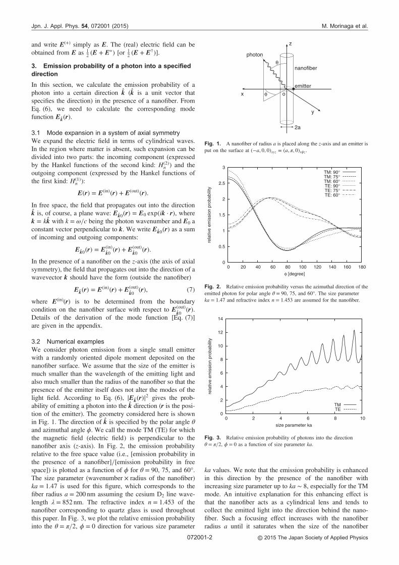
3.2 Numerical examplesWe consider photon emission from a single small emitterwith a randomly oriented dipole moment deposited on thenanofiber surface. We assume that the size of the emitter ismuch smaller than the wavelength of the emitting light andalso much smaller than the radius of the nanofiber so that thepresence of the emitter itself does not alter the modes of thelight field. According to Eq. (6), jEk̂ðrÞj2 gives the prob-ability of emitting a photon into the k̂ direction (r is the posi-tion of the emitter). The geometry considered here is shownin Fig. 1. The direction of k̂ is specified by the polar angle θand azimuthal angle ϕ. We call the mode TM (TE) for whichthe magnetic field (electric field) is perpendicular to thenanofiber axis (z-axis). In Fig. 2, the emission probabilityrelative to the free space value (i.e., [emission probability inthe presence of a nanofiber]=[emission probability in freespace]) is plotted as a function of ϕ for θ = 90, 75, and 60°.The size parameter (wavenumber × radius of the nanofiber)ka = 1.47 is used for this figure, which corresponds to thefiber radius a = 200 nm assuming the cesium D2 line wave-length λ = 852 nm. The refractive index n = 1.453 of thenanofiber corresponding to quartz glass is used throughoutthis paper. In Fig. 3, we plot the relative emission probabilityinto the θ = π=2, ϕ = 0 direction for various size parameter
ka values. We note that the emission probability is enhancedin this direction by the presence of the nanofiber withincreasing size parameter up to ka ∼ 8, especially for the TMmode. An intuitive explanation for this enhancing effect isthat the nanofiber acts as a cylindrical lens and tends tocollect the emitted light into the direction behind the nano-fiber. Such a focusing effect increases with the nanofiberradius a until it saturates when the size of the nanofiber
photon
x
y
z
o
emitter
φ
θnanofiber
2a
Fig. 1. A nanofiber of radius a is placed along the z-axis and an emitter isput on the surface at ð�a; 0; 0Þxyz ¼ ða; �; 0Þr�z.
0
0.5
1
1.5
2
2.5
3
0 20 40 60 80 100 120 140 160 180
rela
tive
emis
sion
pro
babi
lity
φ [degree]
TM: 90°TM: 75°TM: 60°TE: 90°TE: 75°TE: 60°
Fig. 2. Relative emission probability versus the azimuthal direction of theemitted photon for polar angle θ = 90, 75, and 60°. The size parameterka = 1.47 and refractive index n = 1.453 are assumed for the nanofiber.
0
2
4
6
8
10
12
14
0 2 4 6 8 10
rela
tive
emis
sion
pro
babi
lity
size parameter ka
TMTE
Fig. 3. Relative emission probability of photons into the directionθ = π=2, ϕ = 0 as a function of size parameter ka.
Jpn. J. Appl. Phys. 54, 072001 (2015) M. Morinaga et al.
072001-2 © 2015 The Japan Society of Applied Physics

reaches the geometrical optics region (a ≳ �, i.e., ka ≳ 2�).Note that in the small fiber radius limit ka → 0 (i.e., inthe static field limit), the relative emission probability ofthe TM mode converges to 1, whereas that of the TE modeapproaches ½2=ðm2 þ 1Þ�2 < 1. For the general azimuthalangle ϕ and θ = π=2, this limit of the TE mode is shown to be4(m4 sin2ϕ + cos2ϕ)=(m2 + 1)2, whereas that of the TMmode is always 1.
4. Enhancement factor of detection probability
We consider the experimental scheme used in Ref. 12 andestimate how much detection by an external detector isenhanced (or reduced) by the presence of a nanofiber. Thegeometry of the experimental setup to measure the emissioninto the radiation modes is shown in Fig. 4. An objective lenscentered at the x-axis collects emitted photons from anemitter into a photodetector. All emitted photons directedwithin a solid angle determined by the numerical aperture NAof the objective lens (NA = 0.6) move into the detector, i.e.,photons in the direction ð�; �Þ satisfying sin � cos� �ð1 � NA2Þ1=2 are detected. Thus, the enhancement factor(ratio of the detection rates of photons in the presence=absence of a nanofiber) for this system is obtained byaveraging the relative emission probabilities calculated in theprevious section over the solid angle of the objective lens.The azimuthal position of the emitter has also some distribu-tion around ϕ = π (ϕe = 0). Figure 5 shows the estimatedenhancement factors for an emitter at ða; �; 0Þr�z for the TMand TE modes, and their average, whereas in Fig. 6 we showthe total enhancement factors (averages of the TE and TMmodes) for different azimuthal positions of the emitter ϕe = 0,15, 30, 45, 90, 135, and 180°. From Fig. 6, we see that theenhancing effect decreases rapidly with increasing ϕe forka ≳ 4. This can be qualitatively explained by noting thatbecause of the strong focusing effect in that parameter region,the photon emission pattern is highly directional and theenhancement occurs only within the angle of this directivity.Under the experimental conditions in Ref. 12, emitters aresupposed to distribute over ��e0 < �e < �e0 with �e0 ≲90°. In Fig. 7, the enhancement factors 90� and 45� areplotted assuming a uniform distribution of azimuthal positionϕe of the emitter over −90 < ϕe < 90° and −45 < ϕe < 45°,respectively. Also, the enhancement factor ζtotal for theradiation into the whole solid angle Ω = 4π is plotted. � ¼
90�=total or 45�=total gives the correction factor introducedat the end of Sect. 1 that is used to estimate the couplingefficiency from the experimental data. In the experimentin Ref. 12, the correction factor � ¼ 90�=total was used todetermine the coupling efficiency.
x
y
z
o
emitterφe
nanofiber
objective lensphoto-detector
φ
θ
Fig. 4. External detection scheme of Ref. 12. An emitter (quantum dot) isput on the nanofiber surface at ða; � � �e; 0Þr�z, and an objective lens placedon the + side of the x-axis collects emitted photons into a photodetector.
0.5
1
1.5
2
2.5
3
3.5
4
0 2 4 6 8 10
enha
ncem
ent f
acto
r
size parameter ka
TMTE
average
Fig. 5. Enhancement factor for the external detection rate assuming thatthe emitter is positioned at ða; �; 0Þr�z (i.e., ϕe = 0).
0.5
1
1.5
2
2.5
3
3.5
4
0 2 4 6 8 10
enha
ncem
ent f
acto
r
size parameter ka
0°15°30°45°90°
135°180°
Fig. 6. Enhancement factors for various azimuthal emitter positions.
0.8
1
1.2
1.4
1.6
1.8
2
2.2
2.4
2.6
0 2 4 6 8 10
enha
ncem
ent f
acto
r
size parameter ka
-45°..45°-90°..90°
total
Fig. 7. Enhancement factors 45� and 90� assuming a uniform distributionof azimuthal position ϕe of the emitter over the ranges −45 to 45° and −90 to90°, respectively. The enhancement factor ζtotal for the radiation into thewhole solid angle is also plotted.
Jpn. J. Appl. Phys. 54, 072001 (2015) M. Morinaga et al.
072001-3 © 2015 The Japan Society of Applied Physics

5. Conclusions
The photon field modified by the presence of a nanofiber ismode-expanded by a set of mode functions classified by theoutgoing direction. Using this expansion, the relative emis-sion probability into a specific direction in the presence ofa nanofiber is calculated. Also, the enhancing effect on thedetection rate of photons by a detector placed outside thenanofiber is estimated for a realistic experimental scheme. Bychanging the incoming wave (Hð2Þ
n ) with the outgoing wave(Hð1Þ
n ), this method can also be applied to evaluate the photonfield when an external radiation is incident on the nanofiber.Such examples include the fabrication of a photonic crystalstructure on an optical nanofiber using a femtosecond laserthat has been realized recently.28)
Acknowledgements
We thank Fam Le Kien and Yoko Miyamoto for helpfulcomments and suggestions. This work is partly supported bya Grant-in-Aid for Scientific Research 21540407 and theStrategic Innovation Project by Japan Science and Technol-ogy Agency.
Appendix: Mode function Ek̂ðr Þ
In this appendix, we derive the explicit form of the modefunction Ek̂ðrÞ introduced in Eq. (7) by solving the boundarycondition on the nanofiber surface. The derivation is self-contained assuming only a small amount of knowledge ofbasic properties of Bessel functions. The symbol m is usedfor the refractive index of the material (nanofiber) in this
appendix, which we adopt from the notation in Ref. 29. Thegeneral description of the light scattering by a dielectric rightcircular cylinder is found in Refs. 30 and 31. We choosea coordinate such that the z-axis is the axis of the nanofiberand the wavevector k lies in the xz-plane, so that k ¼kðsin �0; 0; cos �0Þxyz with θ0 being the angle between k andthe z-axis. For a plane wave (i.e., in free space),
Ek̂0ðrÞ ¼ E0eik�r ¼ E0 e
ikr sin �0 cos�eikz cos �0 ðA:1Þwith E0 ⊥ k. From r E ¼ �ð@H=@tÞ,
Hk̂0ðrÞ ¼ H0 eikr sin �0 cos�eikz cos �0 ðA:2Þ
with H0 ¼ i k! k̂ E0. In the following, we use the formula
eikr sin �0 cos� ¼X1n¼�1
inJnðkr sin �0Þe�in�:
A.1 TM modeFor the TM mode, E0 and H0 in (A.1) and (A.2) are given by
E0 ¼ ETM0 E0ð�cos �0; 0; sin �0Þxyz
¼ E0ð�cos �0 cos�;�cos �0 sin�; sin �0Þr�zH0 ¼ HTM
0 H0ð0;�1; 0Þxyz¼ H0ðsin�;�cos�; 0Þr�z; ðA:3Þ
where H0 ¼ ikE0=ð!Þ, and we use in this appendix thenotation ( )rϕz to express a vector by its components tangentialto the cylindrical coordinates [i.e., v ¼ ðvr; v�; vzÞr�z withvr ¼ vx cos� � vy sin� and v� ¼ vx sin� þ vy cos�]. Eachcomponent of the electric field ETM
k̂0ðrÞ Ek̂0ðrÞ with E0
defined in Eq. (A·3) is transformed as
ETMk̂0r
ðrÞ ¼ �E0 cos �0 cos�X1n¼�1
inJnðkr sin �0Þe�in�eihz
¼ � 1
2E0 cos �0
X1n¼�1
inþ1fJnþ1ðkr sin �0Þ � Jn�1ðkr sin �0Þge�in�eihz
¼ E0 cos �0X1n¼�1
inþ1J0nðkr sin �0Þe�in�eihz;
ETMk̂0�
ðrÞ ¼ �E0 cos �0 sin�X1n¼�1
inJnðkr sin �0Þe�in�eihz
¼ � 1
2E0 cos �0
X1n¼�1
infJnþ1ðkr sin �0Þ þ Jn�1ðkr sin �0Þge�in�eihz
¼ �E0 cos �0X1n¼�1
innJnðkr sin �0Þ
kr sin �0e�in�eihz;
ETMk̂0z
ðrÞ ¼ E0 sin �0X1n¼�1
inJnðkr sin �0Þe�in�eihz;
with h k cos �0. Defining � kr sin �0, finally
ETMk̂0
ðrÞ ¼ E0
X1n¼�1
JLn ð�; �0Þe�in�eihz;
where JLn are defined as
JLn ð�; �Þ ¼ in
i cos �dJnð�Þd�
� cos �nJnð�Þ
�
sin �Jnð�Þ
0BBBB@
1CCCCA
r�z
:
In the case of magnetic field HTMk̂0
ðrÞ Hk̂0ðrÞ with H0 defined in Eq. (A·3), similarly,
Jpn. J. Appl. Phys. 54, 072001 (2015) M. Morinaga et al.
072001-4 © 2015 The Japan Society of Applied Physics

HTMk̂0
ðrÞ ¼ H0
X1n¼�1
JTn ð�Þe�in�eihz; ðA:4Þ
where JTn are defined as
JTn ð�Þ ¼ in
nJnð�Þ�
idJnð�Þd�
0
0BBBB@
1CCCCA
r�z
:
In the presence of a nanofiber, outside the nanofiber, the mode function ETMk̂
can be written as
ETMk̂
ðrÞ ¼ 1
2E0
X1n¼�1
fb0nHLð2Þn ð�Þ þ a0nH
Tð2Þn ð�Þ þHLð1Þ
n ð�Þge�in�eihz
¼ E0
X1n¼�1
fbnHLð2Þn ð�Þ þ anH
Tð2Þn ð�Þ þ JLn ð�; �0Þge�in�eihz; ðA:5Þ
where bn ¼ 12ðb0n � 1Þ, an ¼ 1
2a0n,
HLðqÞn ð�Þ ¼ in
i cos �0dHðqÞ
n ð�Þd�
� cos �0nHðqÞ
n ð�Þ�
sin �0HðqÞn ð�Þ
0BBBBB@
1CCCCCA
r�z
with q = 1, 2, and
HTð2Þn ð�Þ ¼ in
nHð2Þn ð�Þ�
idHð2Þ
n ð�Þd�
0
0BBBBB@
1CCCCCA
r�z
:
The coefficients bn and an [and dn and cn in Eq. (A·7)] are to bedetermined from the boundary conditions on the nanofibersurface. Similarly, for the magnetic field,
HTMk̂
ðrÞ ¼ H0
X1n¼�1
fbnHTð2Þn ð�Þ � anH
Lð2Þn ð�Þ þ JTn ð�; �0Þge�in�eihz: ðA:6Þ
Inside the nanofiber,
ETMk̂
ðrÞ ¼ E0
X1n¼�1
fdnJLn ð�0; �Þ þ cnJTn ð�0Þge�in�eihz
HTMk̂
ðrÞ ¼ mH0
X1n¼�1
fdnJTn ð�0; �Þ � cnJLn ð�0Þge�in�eihz;
ðA:7Þ
where θ satisfies mk cos θ = h and �0 ¼ ðm2k2 � h2Þ1=2r ¼ mkr sin �. The boundary conditions under which the tangentialcomponents of the electric and magnetic fields are continuous inside and outside the nanofiber surface can be written in the form
Au ¼ v; ðA:8Þwhere
A ¼
n
�scos �0H
ð2Þn ð�sÞ �iHð2Þ0
n ð�sÞ � n
�0scos �Jnð�0sÞ iJ0nð�0sÞ
� sin �0Hð2Þn ð�sÞ 0 sin �Jnð�0sÞ 0
�iHð2Þ0n ð�sÞ � n
�scos �0H
ð2Þn ð�sÞ imJ0nð�0sÞ
mn
�0scos �Jnð�0sÞ
0 sin �0Hð2Þn ð�sÞ 0 �m sin �Jnð�0sÞ
0BBBBBBB@
1CCCCCCCA
with �s ¼ ka sin �0 ¼ ðk2 � h2Þ1=2a, �0s ¼ ðm2k2 � h2Þ1=2a ¼mka sin � (a is the radius of the nanofiber), and
u ¼
bn
an
dn
cn
0BBB@
1CCCA; v ¼
� n
�scos �0Jnð�sÞ
sin �0Jnð�sÞiJ0nð�sÞ
0
0BBBBB@
1CCCCCA: ðA:9Þ
The boundary conditions for the normal components of theelectric and magnetic fields are automatically satisfied if
Eq. (A·8) is fulfilled. (A.8) can be solved as u = A−1v, or
ui ¼ detAi
detA; ðA:10Þ
where Ai is A with the ith column replaced by v. In the case ofθ0 = θ = π=2, TM and TE modes are decoupled and theboundary conditions are reduced to an = cn = 0 and
bnH0ð2Þn ð�sÞ þ J0nð�sÞ ¼ mdnJ
0nðm�sÞ
bnHð2Þn ð�sÞ þ Jnð�sÞ ¼ dnJnðm�sÞ; ðA:11Þ
Jpn. J. Appl. Phys. 54, 072001 (2015) M. Morinaga et al.
072001-5 © 2015 The Japan Society of Applied Physics

leading to
bn ¼ � mJ0nðm�sÞJnð�sÞ � Jnðm�sÞJ0nð�sÞmJ0nðm�sÞHð2Þ
n ð�sÞ � Jnðm�sÞHð2Þ0n ð�sÞ
: ðA:12Þ
A.2 TE modeIn the case of the TE mode, similarly, E0 in Eq. (A·1) isgiven by
E0 ¼ ETE0 E0ð0;�1; 0Þxyz ¼ E0ðsin�;�cos�; 0Þr�z:
ðA:13ÞComparing this with HTM
0 in Eqs. (A·3) and (A·4), we obtain
ETEk̂0ðrÞ ¼ E0
X1n¼�1
JTn ð�Þe�in�eihz:
In the presence of a nanofiber, outside the nanofiber,
ETEk̂ðrÞ ¼ E0
X1n¼�1
fbnHLð2Þn ð�Þ þ anH
Tð2Þn ð�Þ þ JTn ð�Þge�in�eihz
HTEk̂ðrÞ ¼ H0
X1n¼�1
fbnHTð2Þn ð�Þ � anH
Lð2Þn ð�Þ � JLn ð�Þge�in�eihz
instead of Eqs. (A·5) and (A·6). Inside the nanofiber, the fields are again the sum of JLn and JTn as in the case of the TM mode[Eq. (A·7)]:
ETEk̂ðrÞ ¼ E0
X1n¼�1
fdnJLn ð�0; �Þ þ cnJTn ð�0Þge�in�eihz
HTEk̂ðrÞ ¼ mH0
X1n¼�1
fdnJTn ð�0; �Þ � cnJLn ð�0Þge�in�eihz:
ðA:14Þ
Note that we use the same symbols bn, an, dn, and cn for thefield coefficients, but their values are different for the TM andTE modes. The boundary conditions and their solution havethe same form as Eqs. (A·8) and (A·10), but v is nowreplaced with
v ¼
iJ0nð�sÞ0
n
�scos �0Jnð�sÞ
� sin �0Jnð�sÞ
0BBBB@
1CCCCA: ðA:15Þ
In the case of θ0 = π=2, boundary conditions reduce to
anHð2Þn ð�sÞ þ Jnð�sÞ ¼ mcnJnðm�sÞ
anH0ð2Þn ð�sÞ þ J0nð�sÞ ¼ cnJnðm�sÞ
ðA:16Þ
and bn = dn = 0, which lead to
an ¼ � J0nðm�sÞJnð�sÞ � mJnðm�sÞJ0nð�sÞJ0nðm�sÞHð2Þ
n ð�sÞ � mJnðm�sÞHð2Þ0n ð�sÞ
:
1) C. Santori, D. Fattal, and Y. Yamamoto, Single-Photon Devices andApplications (Wiley-VCH, Weinheim, 2010) Chap. 1.
2) V. V. Klimov and M. Ducloy, Phys. Rev. A 69, 013812 (2004).3) F. L. Kien, S. Dutta Gupta, V. I. Balykin, and K. Hakuta, Phys. Rev. A 72,
032509 (2005).4) K. P. Nayak, P. N. Melentiev, M. Morinaga, F. L. Kien, V. I. Balykin, and
K. Hakuta, Opt. Express 15, 5431 (2007).5) A. Stiebeiner, O. Rehband, R. Garcia-Fernandez, and A. Rauschenbeutel,
Opt. Express 17, 21704 (2009).6) E. Vetsch, D. Reitz, G. Sagué, R. Schmidt, S. T. Dawkins, and A.
Rauschenbeutel, Phys. Rev. Lett. 104, 203603 (2010).7) M. Das, A. Shirasaki, K. Nayak, M. Morinaga, F. L. Kien, and K. Hakuta,
Opt. Express 18, 17154 (2010).8) M. Fujiwara, K. Toubaru, T. Noda, H. Zhao, and S. Takeuchi, Nano Lett.
11, 4362 (2011).9) M. Davanço, M. T. Rakher, W. Wegscheider, D. Schuh, A. Badolato, and
K. Srinivasan, Appl. Phys. Lett. 99, 121101 (2011).10) A. Goban, K. S. Choi, D. J. Alton, D. Ding, C. Lacroûte, M. Pototschnig, T.
Thiele, N. P. Stern, and H. J. Kimble, Phys. Rev. Lett. 109, 033603 (2012).11) R. Yalla, K. P. Nayak, and K. Hakuta, Opt. Express 20, 2932 (2012).12) R. Yalla, F. L. Kien, M. Morinaga, and K. Hakuta, Phys. Rev. Lett. 109,
063602 (2012).13) T. Schröder, M. Fujiwara, T. Noda, H.-Q. Zhao, O. Benson, and S.
Takeuchi, Opt. Express 20, 10490 (2012).14) J. D. Thompson, T. G. Tiecke, N. P. de Leon, J. Feist, A. V. Akimov, M.
Gullans, A. S. Zibrov, V. Vuletic, and M. D. Lukin, Science 340, 1202(2013).
15) S. Chonan, S. Kato, and T. Aoki, Sci. Rep. 4, 4785 (2014).16) R. Yalla, M. Sadgrove, K. P. Nayak, and K. Hakuta, Phys. Rev. Lett. 113,
143601 (2014).17) S.-P. Yu, J. D. Hood, J. A. Muniz, M. J. Martin, R. Norte, C.-L. Hung,
S. M. Meenehan, J. D. Cohen, O. Painter, and H. J. Kimble, Appl. Phys.Lett. 104, 111103 (2014).
18) L. Liebermeister, F. Petersen, A. v. Münchow, D. Burchardt, J.Hermelbracht, T. Tashima, A. W. Schell, O. Benson, T. Meinhardt, A.Krueger, A. Stiebeiner, A. Rauschenbeutel, H. Weinfurter, and M. Weber,Appl. Phys. Lett. 104, 031101 (2014).
19) M. Almokhtar, M. Fujiwara, H. Takashima, and S. Takeuchi, Opt. Express22, 20045 (2014).
20) J. Bures and R. Ghosh, J. Opt. Soc. Am. A 16, 1992 (1999).21) L. Tong, J. Lou, and E. Mazur, Opt. Express 12, 1025 (2004).22) F. L. Kien, J. Q. Liang, K. Hakuta, and V. I. Balykin, Opt. Commun. 242,
445 (2004).23) F. L. Kien and K. Hakuta, Phys. Rev. A 77, 013801 (2008).24) F. L. Kien and K. Hakuta, Phys. Rev. A 79, 043813 (2009).25) F. L. Kien and K. Hakuta, Phys. Rev. A 83, 043801 (2011).26) F. L. Kien and A. Rauschenbeutel, Phys. Rev. A 90, 023805 (2014).27) F. L. Kien and A. Rauschenbeutel, Phys. Rev. A 90, 063816 (2014).28) K. P. Nayak and K. Hakuta, Opt. Express 21, 2480 (2013).29) J. A. Stratton, Electromagnetic Theory (McGraw-Hill, New York, 1941)
p. 349.30) J. R. Wait, Electromagnetic Radiation from Cylindrical Structures
(Pergamon, New York, 1959) p. 142.31) C. F. Bohren and D. R. Huffman, Absorption and Scattering of Light by
Small Particles (Wiley, New York, 1983) p. 194.
Jpn. J. Appl. Phys. 54, 072001 (2015) M. Morinaga et al.
072001-6 © 2015 The Japan Society of Applied Physics