passive on-metal uhf rfid tag antenna design
TRANSCRIPT
PASSIVE ON-METAL UHF RFID TAG ANTENNA DESIGN WITH FOLDED T-
MATCH NETWORK
By
Jingwei Zhuo
Senior Thesis in Electrical Engineering
University of Illinois at Urbana-Champaign
Advisor: Jennifer Bernhard
May 2020
ii
Abstract
The radio frequency identification (RFID) industry is expected to witness steady growth as the
demands for reliable asset management and healthcare equipment tracking quickly scale up.
The ultra-high frequency (UHF) RFID system applies radio reader-tag transmissions to identify a
tagged object, with an assigned identification number stored in an RFID integrated circuit (IC). A
problem facing the RFID tag antenna performance on metal is that any metal nearby can detune
and temper the tag antenna. This problem has hampered the endeavor to popularize RFID
technology.
In this thesis, a half-wavelength microstrip resonator with folded dipoles and modified T-match
networks is proposed to enhance the robustness of an antenna on a metallic object. The T-
match network is a common technique for guiding current and improving directivity in passive
RFID tag antenna design. Here, an equivalent circuit model is followed by given design rules
and reasonable analysis. The results show promise for the capability of a tuned antenna to
overcome the influence of a metal plane beneath, with minimum return loss and reasonable
gain. The proposed RFID antenna design is simulated in Ansoft HFSS 18.2.
Subject Keywords: RFID; UHF; folded dipoles; modified T-match

iii
Acknowledgments
I thank my supervisor, Prof. Bernhard, for assisting me with valuable comments and insightful
guidance. Also, I thank Mrs. Kaiser from Alien Technology for her generous donation of the
Higgs-9 RFID chip. My special appreciation goes to graduate student Shuo Liu for offering
experience and resolving problems in HFSS simulation.
Finally, I would like to express my love and gratitude to my family who provides all the possible
support and resources that enable my study in the ECE department at UIUC.

iv
Contents
1. Introduction .............................................................................................................................................. 1
1.1 Background ......................................................................................................................................... 1
1.2 Gen2 standard ..................................................................................................................................... 1
1.3 Passive RFID Systems Basics................................................................................................................ 3
1.4 Thesis Organization ............................................................................................................................. 8
2. Literature Review ...................................................................................................................................... 9
3. Antenna Analysis & Design ..................................................................................................................... 11
3.1 RFID Tag Antenna Design Requirement ............................................................................................ 11
3.2 Antenna Topology ............................................................................................................................. 14
4. Simulation & Analysis .............................................................................................................................. 17
5. Conclusion ............................................................................................................................................... 22
References .................................................................................................................................................. 23
1
1. Introduction
1.1 Background This chapter provides a comprehensive overview and introduction to the radio frequency
identification (RFID) system. Section 1.2 briefly discusses the history of RFID technology and
introduces the globally-accepted Gen2 protocol that standardizes communication between the
interrogator (reader) and the transponder (tag). Section 1.3 focuses on mechanisms of reader
and passive tags in the ultra-high frequency (UHF) RFID system. Section 1.4 provides an
overview of the thesis.
1.2 Gen2 standard RFID is the use of RF signal to identify tagged objects without physical contact. Modern RFID
technology can be traced back to Mario Cardullo’s patent of a passive, read-write RFID tag with
memory in 1973 [1]. In 2004, GS1 EPCglobal developed Electronic Product Code (EPC) as an
open standard for RFID implementation. In 2014, the RAIN Alliance was founded to promote
UHF RFID applications similarly to other wireless technology organizations including the NFC
Forum and WiFi Alliance.
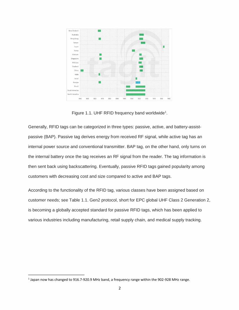
RAIN adopts GS1 UHF Gen2 protocol in ISO/IEC 18000-6C, which standardizes RFID systems
operating in the 860-960 MHz frequency range in Type C. Meanwhile, the Gen2 protocol has
incorporated the frequency band and performance to be used worldwide, as each country
adopts a frequency band that best fits within existing regulations. The ISO/IEC 18000-6C
standard adopts primarily two main frequency bands across the world, 902-928 MHz (USA,
regulated by FCC) and 865-868 MHz (Europe, regulated by ETSI), as shown in Fig. 1.1.
2
Figure 1.1. UHF RFID frequency band worldwide1.
Generally, RFID tags can be categorized in three types: passive, active, and battery-assist-
passive (BAP). Passive tag derives energy from received RF signal, while active tag has an
internal power source and conventional transmitter. BAP tag, on the other hand, only turns on
the internal battery once the tag receives an RF signal from the reader. The tag information is
then sent back using backscattering. Eventually, passive RFID tags gained popularity among
customers with decreasing cost and size compared to active and BAP tags.
According to the functionality of the RFID tag, various classes have been assigned based on
customer needs; see Table 1.1. Gen2 protocol, short for EPC global UHF Class 2 Generation 2,
is becoming a globally accepted standard for passive RFID tags, which has been applied to
various industries including manufacturing, retail supply chain, and medical supply tracking.
1 Japan now has changed to 916.7-920.9 MHz band, a frequency range within the 902-928 MHz range.

3
EPCglobal Tag Class
Type of Tag Feature Programming
Class 0 Passive Read Only Programmed by the manufacturer
Class 1 Passive Write Once, Read Many Programmed by the customer; non-reprogrammed
Class 2 Passive Read & Write Memory reprogrammable
Class 3 Battery Assisted Passive
Read & Write Memory reprogrammable
Class 4 Active Read-Write Active tag with built-in circuitry, can communicate with other
tags and readers
reprogrammable
Class 5 Active Similar to Class 4 tags but with additional functionality; can provide power to other tags and communicate with devices other
than readers
reprogrammable
Table 1.1. RFID tag classifications. [2] [3]
1.3 Passive RFID Systems Basics A normal passive RFID system is composed of both reader and tag. The reader, also known as
the interrogator, modulates the information in a high-frequency carrier in UHF domain and
transmits the RF signals to the passive tag. Once the tag receives the energy via the
electromagnetic waves propagated from reader antenna, the chip mounted on the tag is
activated. The remaining energy is modulated with data in the chip and sent back to the reader
via the tag antenna in the form of UHF RF signals. The communication between reader and tag
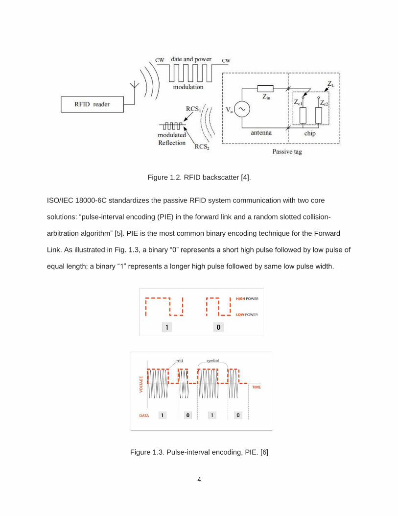
is called backscatter, shown in Fig. 1.2. Backscattering is a bi-directional communication
method, with energy in the Forward Link sent from reader to tag and in the Reverse Link from
tag to reader.
4
Figure 1.2. RFID backscatter [4].
ISO/IEC 18000-6C standardizes the passive RFID system communication with two core
solutions: “pulse-interval encoding (PIE) in the forward link and a random slotted collision-
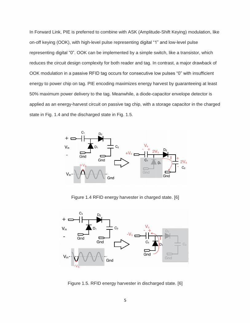
arbitration algorithm” [5]. PIE is the most common binary encoding technique for the Forward
Link. As illustrated in Fig. 1.3, a binary “0” represents a short high pulse followed by low pulse of
equal length; a binary “1” represents a longer high pulse followed by same low pulse width.
Figure 1.3. Pulse-interval encoding, PIE. [6]
5
In Forward Link, PIE is preferred to combine with ASK (Amplitude-Shift Keying) modulation, like
on-off keying (OOK), with high-level pulse representing digital “1” and low-level pulse
representing digital “0”. OOK can be implemented by a simple switch, like a transistor, which
reduces the circuit design complexity for both reader and tag. In contrast, a major drawback of
OOK modulation in a passive RFID tag occurs for consecutive low pulses “0” with insufficient
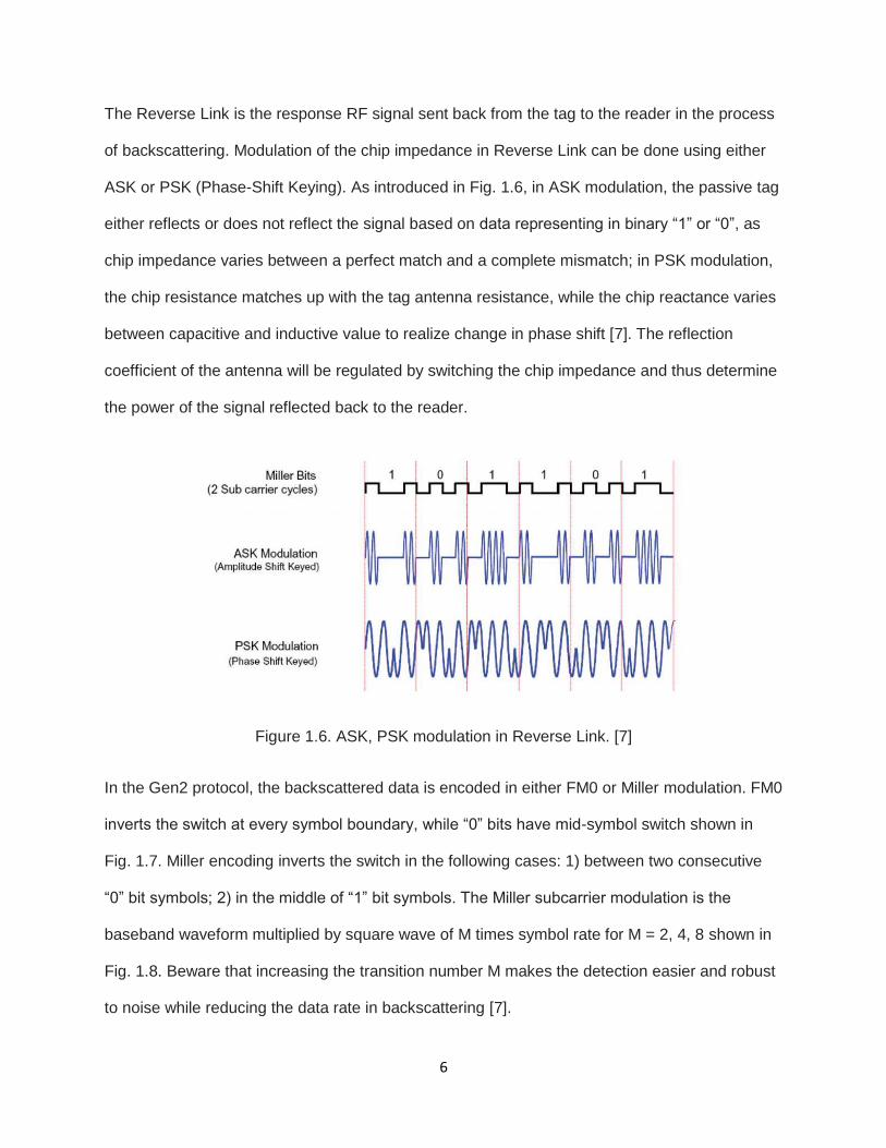
energy to power chip on tag. PIE encoding maximizes energy harvest by guaranteeing at least
50% maximum power delivery to the tag. Meanwhile, a diode-capacitor envelope detector is
applied as an energy-harvest circuit on passive tag chip, with a storage capacitor in the charged
state in Fig. 1.4 and the discharged state in Fig. 1.5.
Figure 1.4 RFID energy harvester in charged state. [6]
Figure 1.5. RFID energy harvester in discharged state. [6]
6
The Reverse Link is the response RF signal sent back from the tag to the reader in the process
of backscattering. Modulation of the chip impedance in Reverse Link can be done using either
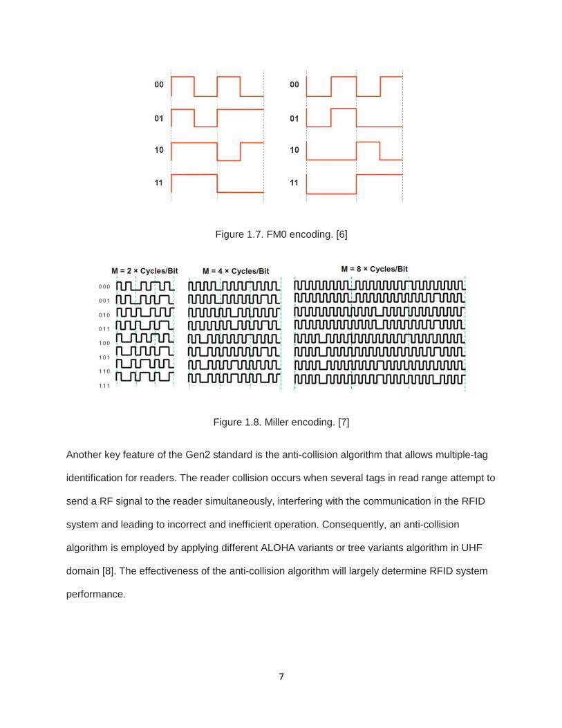
ASK or PSK (Phase-Shift Keying). As introduced in Fig. 1.6, in ASK modulation, the passive tag
either reflects or does not reflect the signal based on data representing in binary “1” or “0”, as
chip impedance varies between a perfect match and a complete mismatch; in PSK modulation,
the chip resistance matches up with the tag antenna resistance, while the chip reactance varies
between capacitive and inductive value to realize change in phase shift [7]. The reflection
coefficient of the antenna will be regulated by switching the chip impedance and thus determine
the power of the signal reflected back to the reader.
Figure 1.6. ASK, PSK modulation in Reverse Link. [7]
In the Gen2 protocol, the backscattered data is encoded in either FM0 or Miller modulation. FM0
inverts the switch at every symbol boundary, while “0” bits have mid-symbol switch shown in
Fig. 1.7. Miller encoding inverts the switch in the following cases: 1) between two consecutive
“0” bit symbols; 2) in the middle of “1” bit symbols. The Miller subcarrier modulation is the
baseband waveform multiplied by square wave of M times symbol rate for M = 2, 4, 8 shown in
Fig. 1.8. Beware that increasing the transition number M makes the detection easier and robust
to noise while reducing the data rate in backscattering [7].
7
Figure 1.7. FM0 encoding. [6]
Figure 1.8. Miller encoding. [7]
Another key feature of the Gen2 standard is the anti-collision algorithm that allows multiple-tag
identification for readers. The reader collision occurs when several tags in read range attempt to
send a RF signal to the reader simultaneously, interfering with the communication in the RFID
system and leading to incorrect and inefficient operation. Consequently, an anti-collision
algorithm is employed by applying different ALOHA variants or tree variants algorithm in UHF
domain [8]. The effectiveness of the anti-collision algorithm will largely determine RFID system
performance.

8
1.4 Thesis Organization The remainder of the thesis is organized as follows. Chapter 2 starts with a literature review that
addresses the anti-metal passive RFID tag. A folded dipole microstrip antenna prototype is
employed and modified in Chapter 3. The design principle and impedance matching technique
are covered in this chapter. Simulation and optimization are accomplished with the
electromagnetic (EM) simulation tool Ansys HFSS 17.2 covered in Chapter 4. Chapter 5 offers a
conclusion and possible future work.
9
2. Literature Review Typically, a UHF passive RFID system works in far field via backscattering, as the passive tag
receives RF signal and wakes up the chip with no internal power source. Due to the backscatter
mechanism, a passive RFID system becomes economically feasible with advantages including
simple tag circuit level design, larger storage capacity, longer lifetime without need to change
battery, and miniature tag size. However, the performance of tag would be severely
compromised with tags attached to metallic objects, as the metal surface strongly detunes the
tag antenna. Nearby metal objects would influence the tag antenna parameters, including but
not limit to input impedance, radiation pattern, bandwidth, and return loss. Research in anti-
metal tags has been conducted due to the customer need for metal-mounted passive tags.
Numerous anti-metal tag antenna topologies have been investigated. A printed inverted F-
antenna (PIFA) with shorting vias connecting feeding layer and ground layer is presented in [9].
Nonetheless, the main drawback of the PIFA topology is concerned with the difficulty to tune the
chip impedance. Besides, the relatively thick substrates and via holes are also not ideal to
fabricate. Another Modified Bowtie Antenna with slot-insertion technique is presented in
combination with a T-match network, with numerical analysis applied to tune the impedance
conjugate and increase the bandwidth [10]. However, the irregular slot inscribed into the
microstrip complicates the fabrication. One intriguing antenna design overlaps three layers of
semicircular dipolar patches with additional mechanism to rotate top patch to tune the overall
antenna impedance and resonant frequency [11]. Such features allow users to manually tune
the tag’s frequency during mass production, but the research problem focused on the structure’s
complexity and robustness to withstand manual-tuning operation that constrain its application.
Necessary tradeoffs have to be made in the process of RFID antenna simulation and
optimization.

10
In Zhang et al. [12], a modified T-match network combined with folded dipoles and short tuning
stubs has been realized in microstrip form. A loop-Bowtie strap feed accompanies with double
T-match loops to enhance the total gain. Introducing a regular slot in the microstrip antenna is
satisfied for fabrication. The antenna prototype is adopted and modified in Chapter 3.

11
3. Antenna Analysis & Design
3.1 RFID Tag Antenna Design Requirement RFID antenna performance can be measured from mainly two aspects: read range and
bandwidth. Read Range can be derived from Friis free-space equation [4], which calculates
received power from reader:
𝑃𝑟 = 𝑃𝑡
𝐺𝑡𝐺𝑟λ2
(4𝜋𝑟)2
(3.1)
As the parameter is defined:
𝑃𝑡: transmitted power.
𝑃𝑟: received power.
𝐺𝑡: transmitted antenna gain.
𝐺𝑟: received antenna gain.
λ: wavelength.
𝑃𝑟: distance between transmitted and received antenna.
In RFID reader-tag communication system, eq. (3.1) becomes:
𝑃𝑡𝑎𝑔 = 𝑃𝑟𝑒𝑎𝑑𝑒𝑟
𝐺𝑟𝑒𝑎𝑑𝑒𝑟𝐺𝑡𝑎𝑔λ2
(4𝜋𝑟)2
(3.2)
Consider ideal case for tag antenna, where antenna polarization, orientation, and backscatter
loss are ignored, such that the only parameter make an influence on received power efficiency
is impedance mismatch between RFID tag antenna and chip mounted on the tag:
𝑃𝑐ℎ𝑖𝑝 = 𝜏𝑃𝑡𝑎𝑔 (3.3)
Here, 𝜏 represents power transmission coefficient (PTC) of received power to chip, the ratio of
available power in chip to the maximum power received by tag. The coefficient 𝜏 can be
obtained from eq. (3.4) [13]:

12
𝜏 = 1 − |𝑍𝑎−𝑍𝑐ℎ𝑖𝑝
𝑍𝑎+𝑍𝐼𝐶𝑐ℎ𝑖𝑝|
2
=4𝑅𝑐ℎ𝑖𝑝𝑅𝑎
(𝑅𝑐ℎ𝑖𝑝+𝑅𝑎)2
+(𝑋𝑐ℎ𝑖𝑝+𝑋𝑎)2
(3.4)
where 𝑍𝑎 = 𝑅𝑎+𝑗𝑋𝑎 is the impedance of the RFID tag antenna and 𝑍𝑐ℎ𝑖𝑝 = 𝑅𝑐ℎ𝑖𝑝+𝑗𝑋𝑐ℎ𝑖𝑝 is
RFID chip impedance.
Assuming that the power available to chip is the minimum threshold power 𝑃𝑡ℎ necessary to
wake up the RFID chip, the following equation can be derived:
𝑃𝑡ℎ = 𝜏𝑃𝑡𝑎𝑔 = 𝜏𝑃𝑟𝑒𝑎𝑑𝑒𝑟
𝐺𝑟𝑒𝑎𝑑𝑒𝑟𝐺𝑡𝑎𝑔λ2
(4𝜋𝑟)2
(3.5)
𝑟 =λ
4𝜋√
𝑃𝑟𝑒𝑎𝑑𝑒𝑟𝐺𝑟𝑒𝑎𝑑𝑒𝑟𝐺𝑡𝑎𝑔𝜏
𝑃𝑡ℎ
(3.6)
In North America, the UHF RFID frequency band within 902-928 MHz is regulated by the
Federal Communications Commission (FCC) with a power constraint, for UHF reader operates
at a maximum transmitted power of 1W (30 dBm), with a maximum EIPR (Equivalent
Isotropically Radiated Power) not exceeding 4W (36 dBm). The RFID EIPR is the product of
transmitted reader power and gain of directional reader antenna. Thus, maximum reading range
can be achieved when:
𝐸𝐼𝑃𝑅 = 𝑃𝑟𝑒𝑎𝑑𝑒𝑟𝐺𝑟𝑒𝑎𝑑𝑒𝑟 = 4 𝑊
(3.7)
The minimum threshold power 𝑃𝑡ℎ can be found on the chip datasheet, with typical value ranges
from -15 dBm to -10 dBm for commercial RFID chips.
The wavelength λ in free-space can be easily calculated from resonant frequency 𝑓𝑐 and light
speed 𝑐:

13
λ =𝑐
𝑓𝑐
(3.8)
Given eq. (3.6), two unknown factors, tag antenna gain 𝐺𝑡𝑎𝑔 and PTC 𝜏 would determine the
valid read range for RFID system, which suggests two key cores for RFID antenna design: gain
and impedance match. Proper impedance match leads to not only enhancement in efficiency,
but also bandwidth selection. The bandwidth can be measured from the S11 parameter, the
reflection coefficient, which is the proportion of energy reflected back measured from input port
[14]:
𝑆11 = 20 log10 |𝑍𝑎 − 𝑍𝑐ℎ𝑖𝑝
∗
𝑍𝑎 + 𝑍𝑐ℎ𝑖𝑝|
(3.9)
𝑍𝑎 is the input impedance of antenna measured form input port and 𝑍𝑐ℎ𝑖𝑝 is input impedance of
chip, while 𝑍𝑐ℎ𝑖𝑝∗ is the complex conjugate of 𝑍𝑐ℎ𝑖𝑝. In simulation, 𝑍𝑐ℎ𝑖𝑝 is a scalar value
equivalent to chip impedance and 𝑍𝑎 is unknown variable in response to change in frequency.
RFID chip can be analyzed as simple parallel RC circuit model to approximate the frequency
response of chip impedance:
𝑍𝑐ℎ𝑖𝑝 = 1
1𝑅 + 𝑗2𝜋𝑓𝐶
= 𝑅
1 + 𝑗2𝜋𝑓𝑅𝐶
(3.10)
where 𝑅 is parallel resistance and 𝐶 is parallel capacitance in the model. In the UHF domain,
the chip impedance would be complex and capacitive. Based on eq. (3.4), the tag antenna
needs to introduce additional inductance in the circuit to maximize the efficiency 𝜏 in the circuit,
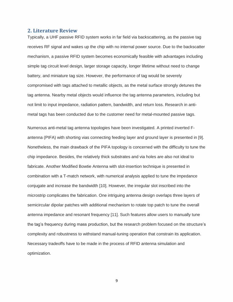
with the complex conjugate impedance match shown in Fig. 3.1. When designing RFID tag
antenna, it is suggested to tune the impedance match with the goal to shift maximum efficiency
peak at resonant frequency 𝑓𝑐.
14
Figure 3.1. Antenna impedance, chip impedance, and range as functions of frequency for a
typical RFID tag. [15]
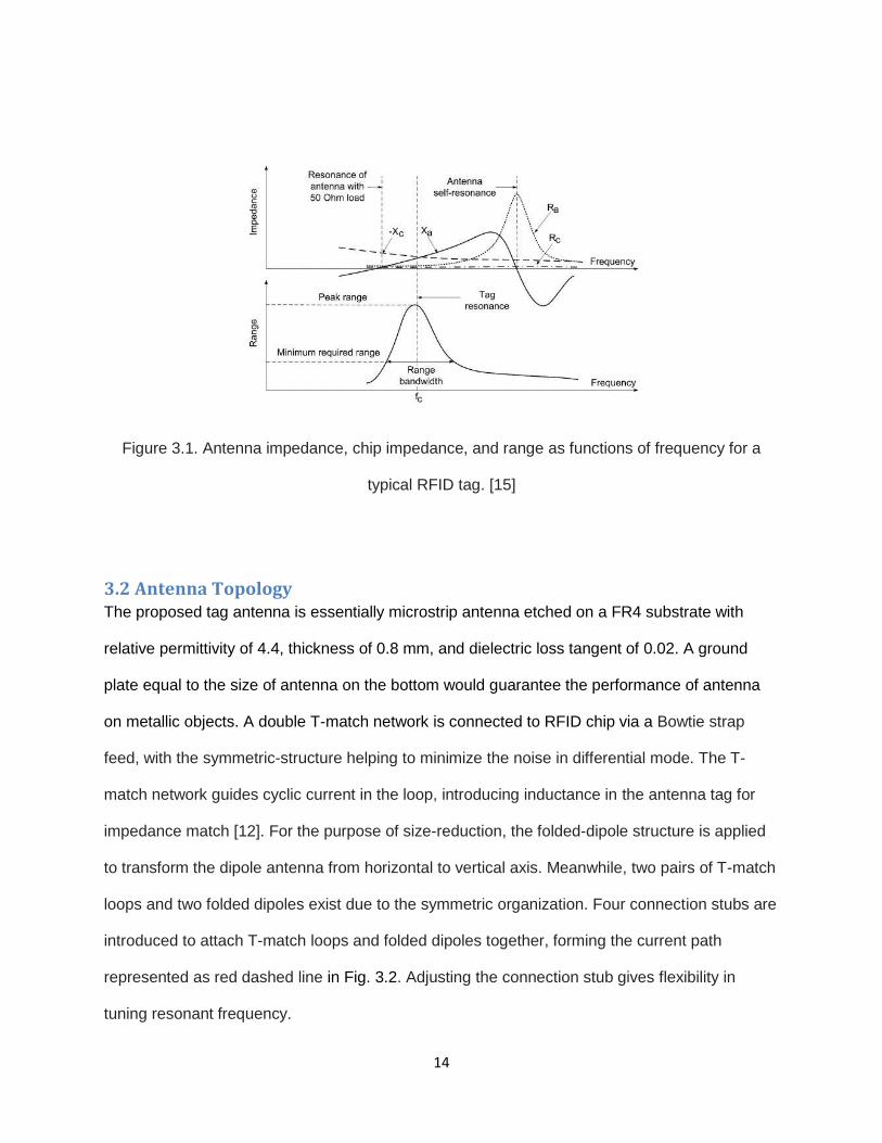
3.2 Antenna Topology The proposed tag antenna is essentially microstrip antenna etched on a FR4 substrate with
relative permittivity of 4.4, thickness of 0.8 mm, and dielectric loss tangent of 0.02. A ground
plate equal to the size of antenna on the bottom would guarantee the performance of antenna
on metallic objects. A double T-match network is connected to RFID chip via a Bowtie strap
feed, with the symmetric-structure helping to minimize the noise in differential mode. The T-
match network guides cyclic current in the loop, introducing inductance in the antenna tag for
impedance match [12]. For the purpose of size-reduction, the folded-dipole structure is applied
to transform the dipole antenna from horizontal to vertical axis. Meanwhile, two pairs of T-match
loops and two folded dipoles exist due to the symmetric organization. Four connection stubs are
introduced to attach T-match loops and folded dipoles together, forming the current path
represented as red dashed line in Fig. 3.2. Adjusting the connection stub gives flexibility in
tuning resonant frequency.
15
(a)
(b)
Figure 3.2. Configuration of proposed antenna in: a) Top view; b) front view.
In this thesis, the Alien Gen2 Higgs-9 chip is adopted, with parallel resistance and capacitance
given by 2500 Ω and 0.85 pF, respectively. The minimum threshold power 𝑃𝑡ℎ during reading is
-17.7 dBm. The resonant frequency 𝑓𝑐 is set at 915 MHz for operation. Updating all known
factors in eq. (3.10), the impedance of Higgs-9 chip can be calculated with value: 𝑍𝑐ℎ𝑖𝑝 = 16 −
𝑗203 Ω.
A typical T-match dipole antenna can be decomposed in segments in the equivalent circuit
model given in Fig 3.3. The major inductance is contributed by the tag antenna, while the folded
dipoles give rise to both inductive and reactive components based on the geometric design. The
main goal for impedance match is to approximate antenna impedance 𝑍𝑎 = 16 + 𝑗203 Ω to
maximize efficiency at resonant frequency 𝑓𝑐 = 915 MHz. Applying dipole antenna theory in
16
microstrip structure, the result of half-wavelength resonator could be calculated from equation
below:
λ𝑚
2=
𝑐
2𝑓𝑐√Ɛr
(3.11)
where Ɛr represents the relative permittivity of substrate used and λ𝑚
2= 81.9mm represents the
half-length of microstrip resonator. Essentially, the current path from dipole end to RFID chip in
Figure 3.2a would approximate half-length λ𝑚
2, which is the priority in antenna design and
optimization.
Figure 3.3, Equivalent circuit model of proposed antenna. [14]
The parameters of proposed antenna are as follows: L = 55 mm, L1 = 15 mm, L2 = 23 mm, L3 =
4 mm, W = 20mm, W1 = 2 mm, W2 = 2 mm, W3 = 2 mm, G1 = 1 mm, G2 = 2 mm, G3 = 1 mm,
G4 = 1 mm, K = 1mm.
17
4. Simulation & Analysis RFID antenna design is accomplished and optimized using Ansys HFSS 17.2 based on the
finite element method (FEM). A 400 × 400 × 0.8mm3 copper plate is applied beneath the
antenna as simulated scenario to test near-metal performance.
The four connection stubs give the flexibility of tuning the folded dipoles for the purpose of
impedance match. The tuning operation would not change the half-length resonator path where
the current flows in Figure 3.2a. It would actually influence the impedance composition of the
folded dipole section. By changing the connection stubs’ positions against the center axis, the
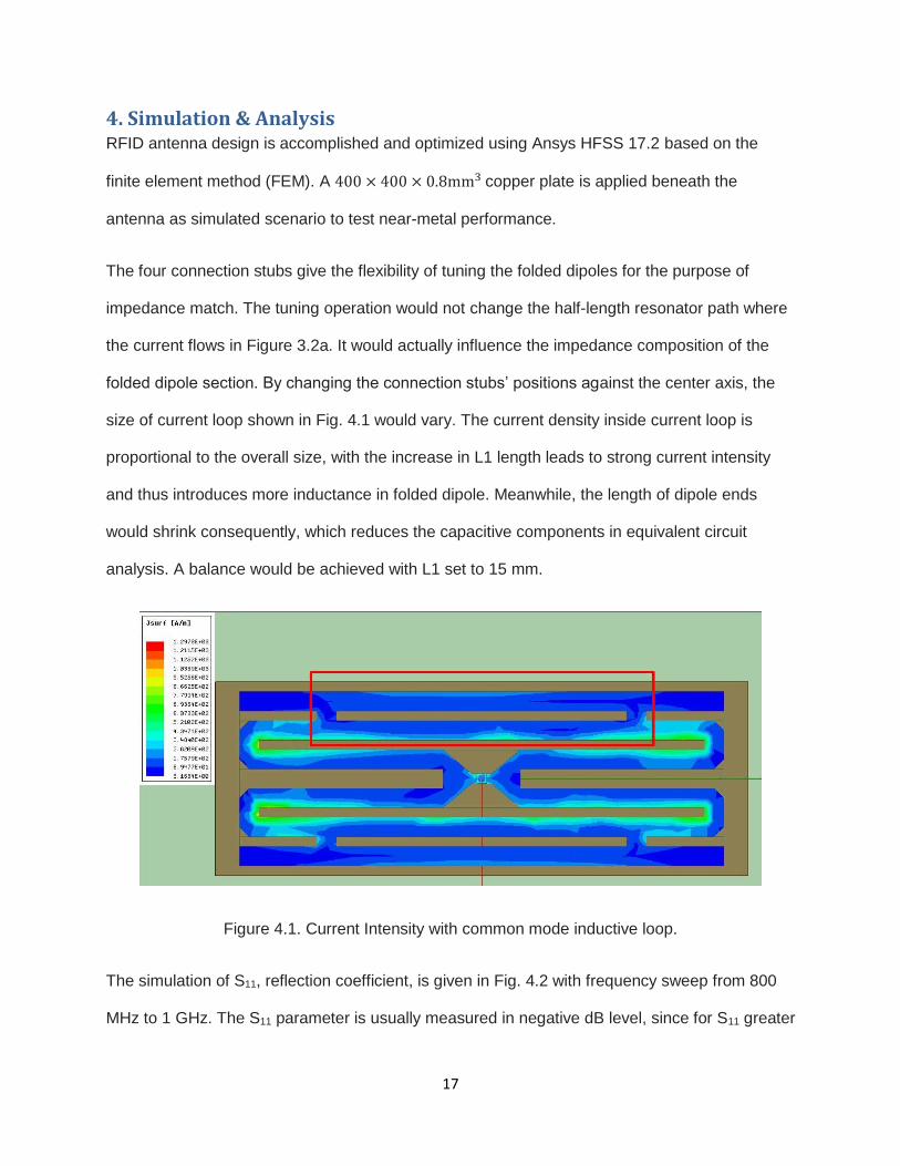
size of current loop shown in Fig. 4.1 would vary. The current density inside current loop is
proportional to the overall size, with the increase in L1 length leads to strong current intensity
and thus introduces more inductance in folded dipole. Meanwhile, the length of dipole ends
would shrink consequently, which reduces the capacitive components in equivalent circuit
analysis. A balance would be achieved with L1 set to 15 mm.
Figure 4.1. Current Intensity with common mode inductive loop.
The simulation of S11, reflection coefficient, is given in Fig. 4.2 with frequency sweep from 800
MHz to 1 GHz. The S11 parameter is usually measured in negative dB level, since for S11 greater
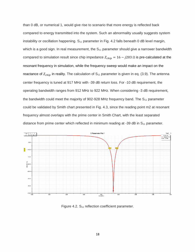
18
than 0 dB, or numerical 1, would give rise to scenario that more energy is reflected back
compared to energy transmitted into the system. Such an abnormality usually suggests system
instability or oscillation happening. S11 parameter in Fig. 4.2 falls beneath 0 dB level margin,
which is a good sign. In real measurement, the S11 parameter should give a narrower bandwidth
compared to simulation result since chip impedance 𝑍𝑐ℎ𝑖𝑝 = 16 − 𝑗203 Ω is pre-calculated at the
resonant frequency in simulation, while the frequency sweep would make an impact on the
reactance of 𝑍𝑐ℎ𝑖𝑝 in reality. The calculation of S11 parameter is given in eq. (3.9). The antenna
center frequency is tuned at 917 MHz with -39 dB return loss. For -10 dB requirement, the
operating bandwidth ranges from 912 MHz to 922 MHz. When considering -3 dB requirement,
the bandwidth could meet the majority of 902-928 MHz frequency band. The S11 parameter
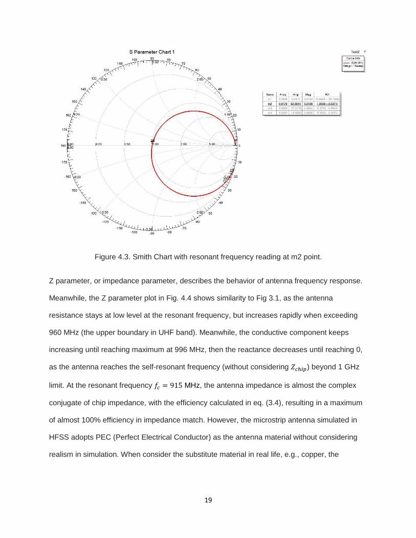
could be validated by Smith chart presented in Fig. 4.3, since the reading point m2 at resonant
frequency almost overlaps with the prime center in Smith Chart, with the least separated
distance from prime center which reflected in minimum reading at -39 dB in S11 parameter.
Figure 4.2. S11 reflection coefficient parameter.
19
Figure 4.3. Smith Chart with resonant frequency reading at m2 point.
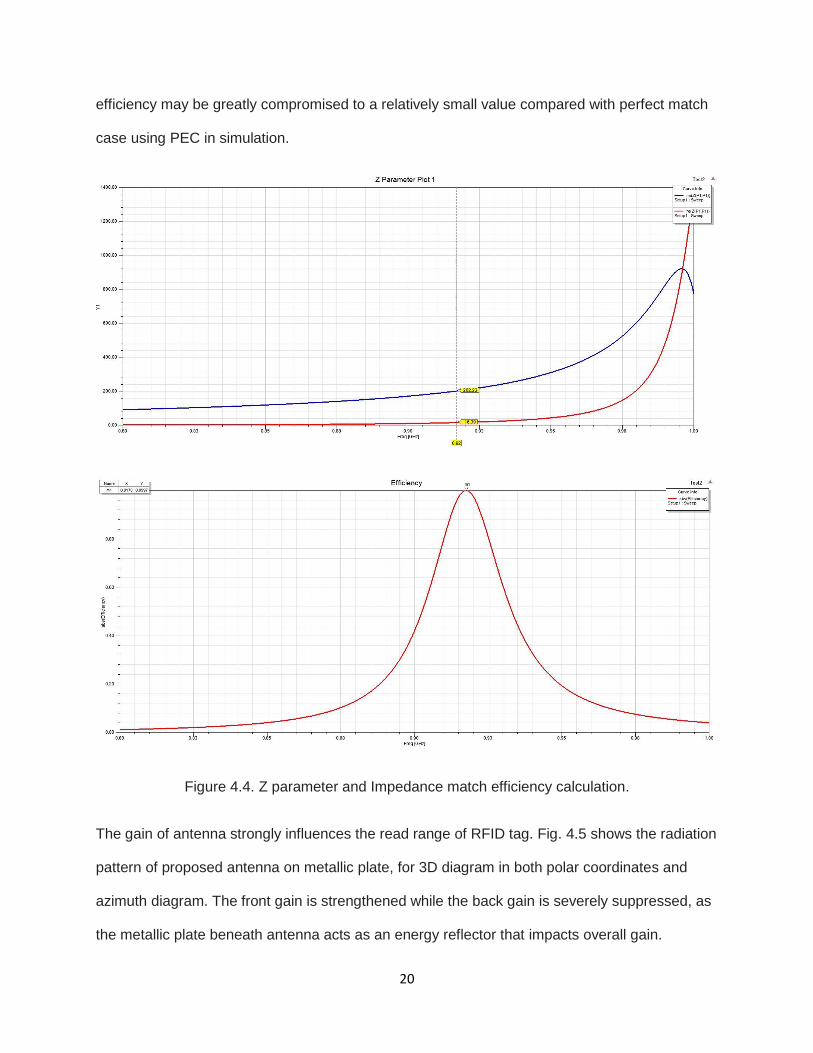
Z parameter, or impedance parameter, describes the behavior of antenna frequency response.
Meanwhile, the Z parameter plot in Fig. 4.4 shows similarity to Fig 3.1, as the antenna
resistance stays at low level at the resonant frequency, but increases rapidly when exceeding
960 MHz (the upper boundary in UHF band). Meanwhile, the conductive component keeps
increasing until reaching maximum at 996 MHz, then the reactance decreases until reaching 0,
as the antenna reaches the self-resonant frequency (without considering 𝑍𝑐ℎ𝑖𝑝) beyond 1 GHz
limit. At the resonant frequency 𝑓𝑐 = 915 MHz, the antenna impedance is almost the complex
conjugate of chip impedance, with the efficiency calculated in eq. (3.4), resulting in a maximum
of almost 100% efficiency in impedance match. However, the microstrip antenna simulated in
HFSS adopts PEC (Perfect Electrical Conductor) as the antenna material without considering
realism in simulation. When consider the substitute material in real life, e.g., copper, the
20
efficiency may be greatly compromised to a relatively small value compared with perfect match
case using PEC in simulation.
Figure 4.4. Z parameter and Impedance match efficiency calculation.
The gain of antenna strongly influences the read range of RFID tag. Fig. 4.5 shows the radiation
pattern of proposed antenna on metallic plate, for 3D diagram in both polar coordinates and
azimuth diagram. The front gain is strengthened while the back gain is severely suppressed, as
the metallic plate beneath antenna acts as an energy reflector that impacts overall gain.

21
Meanwhile, the maximum front gain where θ, φ = 0°, is -15 dB, a relatively low value due to the
fact that the tag antenna is designed to be electrically small, hindering the gain and efficiency of
antenna performance.
Figure 4.5. Z parameter and Impedance match efficiency calculation.
Arguably, such an electrically small antenna design may still perform well in real cases. Read
range can be calculated by applying eq. (3.6), with given result 𝑟 = 2.25 m, assuming that a
maximum EIRP of 4W and efficiency 𝜏 = 100% can be reached (won’t be accessible in the real
case). The simulated reading range is acceptable so far. However, a lot of environmental
constraints are not covered in calculation, e.g., path loss, backscatter loss, which would further
deteriorate the result. On the other hand, a larger read range would also induce collision
problem when a single reader wakes up multiple tags at the same time. However, the anti-
collision algorithm is not the focus of this thesis.

22
5. Conclusion Analysis and simulation of the proposed double T-match network with folded dipoles has been
conducted to overcome the interference induced by the metallic object nearby. The planned
antenna fabrication and measurement have been delayed due to COVID-19, with no step to
further validate the design in reality. Size-reduction has been achieved in design, though the
antenna gain as well as the read range is limited due to the electrically small size of the
microstrip antenna structure. Further antenna fabrication and measurement are necessary to
validate the design and further test the performance. More simulation and testing of the tuning
capacity of the short connection stub are expected to adjust the bandwidth in not only US band
but also global frequency band from 860 MHz to 960 MHz.
23
References [1] Genesis of the Versatile RFID Tag, web page. Available at:
https://www.transformation.dk/www.raven1.net/mcf/news/genesis-of-rfid.htm
Accessed Apr. 2020.
[2] RFID Tags, web page. Available at: https://www.epc-rfid.info/rfid_tags.
[3] J. I. Aguirre, “EPCglobal: a Universal Standard,” M.S. thesis, Massachusetts Institute of Technology,
Cambridge, MA, 2007.
[4] Y. Gao and Z. Zhang, “Analysis and Calculation of Read Distance in Passive Backscatter RFID
Systems,” LISS 2012. 2013, pp. 905-912, Wiley, 2016.
[5] ISO/IEC 18000-63:2015(en), web page. Available at: https://www.iso.org/obp/ui/#iso:std:iso-
iec:18000:-63:en.
Accessed Apr. 2020.
[6] H. Hassanieh, “IoT II: Backscatter,” class note for ECE 463, Department of Electrical and Computer
Engineering, University of Illinois at Urbana-Champaign, 2018.
[7] H. Li, “Development and Implementation of RFID Technology,” in Development and Implementation
of RFID Technology, C. Turcu, Ed. In-Tech, 2009, pp. 1-12.
[8] D. Klair, K. Chin, et al., "A survey and tutorial of RFID anti-collision protocols", IEEE Communications
Surveys & Tutorials, vol. 12, (3) pp. 400-421, 2010.
[9] W.-K. Choi, H.-W. Son, et al., “An RFID tag using a planar inverted-F antenna capable of being suck
to metallic objects,” ETRI J., vol. 28, pp. 216–218, 2006.
[10] D. El-Aziz, T. Abouelnaga, et al., “Analysis and design of UHF Bow-Tie RFID tag antenna input
impedance,” Open J. Antennas Propag., vol. 4, no. 2, pp. 85–107, Jan. 2016.
[11] Y.-H. Niew, K.-Y. Lee, et al., “Patch-loaded semicircular dipolar antenna for metal-mountable UHF
RFID tag design,” IEEE Trans. Antennas Propag. 2019.
[12] Y. J. Zhang, D. Wang, et al., “An adjustable quarter-wavelength meandered dipole antenna with
slotted ground for metallically and airily mounted RFID tag,” IEEE Trans. Antennas Propag., vol. 65,
no. 6, pp. 2890–2898, Jun. 2017.
[13] K.-H. Lin, S.-L. Chen, et al., “A Looped-Bowtie RFID Tag Antenna Design for Metallic Objects,” IEEE
Trans. Antennas Propag., vol. 61, no. 2, pp. 499–505, Feb. 2013.
[14] D. D. Deavours, “Analysis and design of wideband passive UHF-RFID tags using a circuit model,” in
Proc. IEEE Int. Conf. RFID, May 2009, pp. 283–290.

24
[15] K.V.S. Rao, P.V. Nikitin, et al., "Antenna design for UHF RFID tags: a review and a practical
application," IEEE Transactions on Antennas and Propagation, vol. 53, no. 12, pp. 3870- 3876, Dec.
2005