design and implementation of vhf-uhf antenna
TRANSCRIPT
DESIGN AND IMPLEMENTATION OF VHF-UHF ANTENNA WITHNON-FOSTER MATCHING CIRCUIT
A THESIS SUBMITTED TOTHE GRADUATE SCHOOL OF NATURAL AND APPLIED SCIENCES
OFMIDDLE EAST TECHNICAL UNIVERSITY
BY
CIHAN ASCI
IN PARTIAL FULFILLMENT OF THE REQUIREMENTSFOR
THE DEGREE OF MASTER OF SCIENCEIN
ELECTRICAL AND ELECTRONICS ENGINEERING
AUGUST 2018

Approval of the thesis:
DESIGN AND IMPLEMENTATION OF VHF-UHF ANTENNA WITHNON-FOSTER MATCHING CIRCUIT
submitted by CIHAN ASCI in partial fulfillment of the requirements for the degree ofMaster of Science in Electrical and Electronics Engineering Department, MiddleEast Technical University by,
Prof. Dr. Halil KalıpçılarDean, Graduate School of Natural and Applied Sciences
Prof. Dr. Tolga ÇilogluHead of Department, Electrical and Electronics Engineering
Prof. Dr. Özlem Aydın ÇiviSupervisor, Electrical and Electronics Eng. Dept., METU
Examining Committee Members:
Prof. Dr. Gülbin DuralElectrical and Electronics Engineering Dept., METU
Prof. Dr. Özlem Aydın ÇiviElectrical and Electronics Engineering Dept., METU
Assoc. Prof. Dr. Lale AlatanElectrical and Electronics Engineering Dept., METU
Prof. Dr. Özlem ÖzgünElectrical and Electronics Engineering Dept., Hacettepe University
Prof. Dr. Vakur Behçet ErtürkElectrical and Electronics Engineering Dept., Bilkent University
Date:

I hereby declare that all information in this document has been obtained andpresented in accordance with academic rules and ethical conduct. I also declarethat, as required by these rules and conduct, I have fully cited and referenced allmaterial and results that are not original to this work.
Name, Last Name: CIHAN ASCI
Signature :
iv
ABSTRACT
DESIGN AND IMPLEMENTATION OF VHF-UHF ANTENNA WITHNON-FOSTER MATCHING CIRCUIT
Ascı, Cihan
M.S., Department of Electrical and Electronics Engineering
Supervisor : Prof. Dr. Özlem Aydın Çivi
August 2018, 97 pages
Matching networks are widely used in the antenna transmitter and receiver appli-cations and thus they are an essential part of the RF system. Conventional passivematching networks are very broadly used for matching an antenna for a narrow bandof frequencies; however, achieving a broad bandwidth characteristics for electrically–small antennas (ESAs) is not possible with the use of passive matching circuits. ESAspossess a large input reactance and the electrical size of the antenna element is verysmall compared to the wavelength of operation. Non–Foster matching networks canovercome the limitations of passive matching networks and the problems due to elec-trical size of ESAs.
The design and implementation of non–Foster matching networks realized by tran-sistor negative impedance converters is presented in this thesis. Non–Foster match-ing provides a reactive cancellation in the antenna impedance, and thus, overcom-ing the gain-bandwidth limitation accomplishes a broadband operation. The non–Foster matching network is designed for an electrically–small monopole antenna inthe VHF/UHF band. The overall performance is evaluated between 100 MHz and900 MHz for different input power levels. The designed non–Foster circuit can pro-vide impedance matching up to a bandwidth of 600 MHz. Between 100 MHz and900 MHz, it is observed that the imaginary part of the input impedance has been sig-nificantly reduced. The designed non–Foster circuit provides improvement not only
v

for return loss but also antenna gain. The gain measurements are taken in between150 MHz and 500 MHz where 5 to 12 dB gain improvement is recorded. In additionto the non–Foster matching, a reactively–loaded monopole antenna whose physicaldimensions are different is also designed using a genetic algorithm (GA) as a compar-ative study. Among three different reactive loading designs, for the third design forthe thin monopole antenna, an antenna gain better than –10 dB is obtained in between200 MHz and 430 MHz. Two reactively–loaded antenna designs have roughly 200MHz bandwidth and for one other antenna design, 290 MHz bandwidth is achieved.
Keywords: Electrically small monopole antennas, impedance matching, negativeimpedance converters, RF circuits
vi
ÖZ
VHF-UHF BANDINDA BIR ANTENIN VE FOSTER OLMAYANUYUMLAMA DEVRESININ TASARIMI VE GERÇEKLESTIRILMESI
Ascı, Cihan
Yüksek Lisans, Elektrik ve Elektronik Mühendisligi Bölümü
Tez Yöneticisi : Prof. Dr. Özlem Aydın Çivi
Agustos 2018 , 97 sayfa
Uyumlandırma devreleri anten alıcı ve verici devrelerinde sıklıkla kullanılmaktadır veRF sistemlerinin önemli bir bölümünü olusturmaktadır. Pasif uyumlandırma devrelerigenellikle antenlerin dar bir frekans bandında uyumlandırılabilmesi için sıkça kulla-nılan bir yöntemdir. Fakat, elektriksel olarak küçük antenler için genis bant karak-teristigi elde etmek pasif uyumlandırma devreleri ile mümkün olmamaktadır. Küçükantenler giris empedanslarında yüksek reaktans bulundururlar ve anten elemanınınelektriksel boyutu çalısma frekansına karsılık gelen dalgaboyuna göre çok küçüktür.Foster olmayan uyumlandırma devreleri pasif uyumlandırma devrelerinin ve küçükantenlerin elektriksel boyutlarından kaynaklanan problemleri çözebilmektedir.
Bu tez negatif empedans dönüstürücüleri ile gerçeklenmis Foster olmayan uyumlan-dırma devrelerinin tasarım ve uygulanmasını içermektedir. Foster olmayan uyumlan-dırma anten empedansının reaktif kısmını azaltarak ve bunun sonucunda kazanç–bantgenisligi kısıtlamasını asarak antenin genis bantta çalısmasına olanak saglamaktır.Foster olmayan uyumlandırma devresi bir VHF/UHF bandında, bir tek kutuplu küçüktel anten için tasarlanmıstır. Devre performansı 100 MHz ile 900 MHz bandı arasındafarklı giris güç seviyelerine göre incelenmistir. Tasarlanan bu uyumlama devresi enfazla 600 MHz’e kadar bir bantta empedans uyumlaması gerçeklestirebilmektedir.100 MHz ile 900 MHz arasında, giris empedansının reaktif kısmının büyük ölçüde
vii

azaltıldıgı gözlemlenmistir. Geri dönüs kaybı ve anten empedansının iyilestirilmesi-nin yanı sıra, Foster olmayan uyumlandırma devresi anten kazancını da gelistirmek-tedir. Kazanç ölçümleri 150 ile 500 MHz arasında alınmıs olup, kazançta 5 ile 12dB arasında gelisme kaydedilmistir. Ayrıca, karsılastırmalı bir çalısma olması açı-sından, Foster olmayan uyumlandırma devresinin yanı sıra, fiziksel büyüklügü farklıolan baska bir tek kutuplu reaktif yüklü anten genetik algoritma (GA) kullanılaraktasarlanmıstır. Tasarlanan üç farklı tasarım arasından üçüncüsünde, 200 MHz ile 430MHz arasında –10 dB’den daha iyi anten kazancı elde edilmistir. Iki anten tasarımınınbant genisligi yaklasık olarak 200 MHz ölçülürken, diger üçüncü tasarlanan anten iseyaklasık 290 MHz bant genisligine sahiptir.
Anahtar Kelimeler: Tek kutuplu antenler küçük antenler, empedans uyumlandırması,
negatif empedans dönüstürücüleri, RF devreleri
viii

To my family
ix

ACKNOWLEDGMENTS
First of all, I would like to express my sincere thanks to my supervisor Prof. Özlem
Aydın Çivi not only for her valuable supervision and support but also for granting
me the opportunity to strive for my thesis study. I would also like to thank Prof.
Sencer Koç for his guidance and encouragement throughout my thesis work. I am also
indebted to the thesis committee members Assoc. Prof. Lale Alatan, Prof. Gülbin
Dural, Prof. Vakur Behçet Ertürk and Prof. Özlem Özgün for their comments on my
thesis work.
I would moreover thank the good people of ARC–304, Büsra Timur, Efecan Bozulu,
Enis Kobal, Savas Karadag, Semih Küçük, Yigit Haykır and Zafer Tanç for their
friendship, support and help, which make our office a warm workplace. I also wish
to thank Adem Ates for his gentle support and help during the fabrication process of
the work presented in this thesis.
I am also grateful for my dearest friends Alper Soytürk, Berkay Güngördü, Batuhan
Pamuk, Mertkan Yanık, Pelin Gündogmus and Yagız Kushan for their support and
friendship.
I want to express my deepest appreciation to my family; my mother Nilüfer Ascı, my
father Arif Ascı, my sister Zeynep Ascı, and my grandmother Nur Demirtas for their
26 years of support. It would be impossible for me to be in this position without their
encouragement and love.
Finally, last but by no means least, I would like to thank one more person, Aslı
Aykanat, for her understanding and endless support. I will forever be grateful to
her.
x

TABLE OF CONTENTS
ABSTRACT . . . . . . . . . . . . . . . . . . . . . . . . . . . . . . . . . . . . v
ÖZ . . . . . . . . . . . . . . . . . . . . . . . . . . . . . . . . . . . . . . . . . vii
ACKNOWLEDGMENTS . . . . . . . . . . . . . . . . . . . . . . . . . . . . . x
TABLE OF CONTENTS . . . . . . . . . . . . . . . . . . . . . . . . . . . . . xi
LIST OF TABLES . . . . . . . . . . . . . . . . . . . . . . . . . . . . . . . . xiv
LIST OF FIGURES . . . . . . . . . . . . . . . . . . . . . . . . . . . . . . . . xv
LIST OF ABBREVIATIONS . . . . . . . . . . . . . . . . . . . . . . . . . . . xxii
CHAPTERS
1 INTRODUCTION . . . . . . . . . . . . . . . . . . . . . . . . . . . 1
1.1 Motivation . . . . . . . . . . . . . . . . . . . . . . . . . . . 1
1.2 Contributions of the Thesis . . . . . . . . . . . . . . . . . . 6
1.3 Organization of the Thesis . . . . . . . . . . . . . . . . . . . 7
2 ELECTRICALLY–SMALL ANTENNAS . . . . . . . . . . . . . . . 9
2.1 Small Antenna Theory . . . . . . . . . . . . . . . . . . . . . 9
2.1.1 Definitions . . . . . . . . . . . . . . . . . . . . . 9
2.1.2 Fundamental Limits of Electrically–Small Antennas 10
2.2 Monopole Antennas . . . . . . . . . . . . . . . . . . . . . . 12
xi

2.2.1 Input Impedance . . . . . . . . . . . . . . . . . . 13
2.2.2 Stored Energies, Radiation Quality Factor and Band-width . . . . . . . . . . . . . . . . . . . . . . . . 18
3 DESIGN AND IMPLEMENTATION OF A MONOPOLE ANTENNAUSING REACTIVE LOADING . . . . . . . . . . . . . . . . . . . . 23
3.1 Introduction to Reactive Loading . . . . . . . . . . . . . . . 23
3.2 The Thin Monopole Antenna . . . . . . . . . . . . . . . . . 26
3.3 Design of the Loaded Antenna and Matching Network . . . . 27
3.4 Simulated and Measured Results . . . . . . . . . . . . . . . 30
4 NON–FOSTER MATCHING . . . . . . . . . . . . . . . . . . . . . . 35
4.1 Passive and Active Impedance Matching . . . . . . . . . . . 35
4.1.1 Foster Reactance Theorem . . . . . . . . . . . . . 35
4.1.2 Bode–Fano Limit of Passive Lossless MatchingNetworks . . . . . . . . . . . . . . . . . . . . . . 36
4.1.3 An Example of Passive Matching Using LumpedCircuit Elements . . . . . . . . . . . . . . . . . . 37
4.1.4 Non–Foster Impedances . . . . . . . . . . . . . . 39
4.1.5 Basic Impedance Matching Technique . . . . . . . 40
4.2 Negative Impedance Converters . . . . . . . . . . . . . . . . 43
4.2.1 Two-Port Circuit and Parameters . . . . . . . . . . 44
4.2.2 Negative–Gm Oscillators . . . . . . . . . . . . . . 48
4.2.3 Transistor Negative Impedance Converters . . . . . 51
4.2.4 Opamp Negative Impedance Converters . . . . . . 55
4.3 Stability of Negative Impedance Converters . . . . . . . . . 58
4.4 A Brief Review of the Non–Foster Matching Literature . . . 60
xii

5 DESIGN AND IMPLEMENTATION OF NON–FOSTER NETWORK 63
5.1 Design of Non–Foster Network and Antenna . . . . . . . . . 63
5.1.1 Introduction and Design Approach . . . . . . . . . 63
5.1.2 Fabrication of the Non–Foster Network and theAntenna . . . . . . . . . . . . . . . . . . . . . . . 70
5.2 Simulated and Measured Results . . . . . . . . . . . . . . . 71
5.2.1 Return Loss . . . . . . . . . . . . . . . . . . . . . 72
5.2.2 Input Impedance . . . . . . . . . . . . . . . . . . 75
5.2.3 Antenna Gain . . . . . . . . . . . . . . . . . . . . 78
6 CONCLUSION . . . . . . . . . . . . . . . . . . . . . . . . . . . . . 83
6.1 Conclusion and Summary . . . . . . . . . . . . . . . . . . . 83
6.2 Future Work . . . . . . . . . . . . . . . . . . . . . . . . . . 85
REFERENCES . . . . . . . . . . . . . . . . . . . . . . . . . . . . . . . . . . 87
APPENDICES
A TRANSISTOR PARAMETERS . . . . . . . . . . . . . . . . . . . . 91
B ANALYSIS OF SUSSMAN–FORT’S GROUNDED NIC CIRCUIT . 95
xiii

LIST OF TABLES
TABLES
Table 2.1 Summary of the definitions of ESAs based on the product ka. . . . . 9
Table 2.2 Minimum Qrad expressions derived by various authors. . . . . . . . 12
Table 3.1 The design parameters of the reactive loading and matching circuit
entered in the genetic algorithm code in MATLAB®. . . . . . . . . . . . . 29
Table 3.2 The calculated values of the lumped components of reactive loads
and external matching circuit. . . . . . . . . . . . . . . . . . . . . . . . . 30
Table 4.1 Numerical values of the circuit elements utilized in the passive
matching circuit example. . . . . . . . . . . . . . . . . . . . . . . . . . . 40
Table 5.1 Numerical values and usage purposes of the circuit elements utilized
in the non–Foster matching network. . . . . . . . . . . . . . . . . . . . . 71
Table A.1 SOT23 device parasitics model parameters of BFU550A transistor. . 93
Table B.1 Numerical values and usage purposes of the circuit elements utilized
in the grounded NIC circuit. . . . . . . . . . . . . . . . . . . . . . . . . . 96
xiv
LIST OF FIGURES
FIGURES
Figure 2.1 The equivalent circuit representation of Wheeler’s antennas: (a)
Electric dipole. (b) Magnetic dipole. [1, 2] . . . . . . . . . . . . . . . . . 10
Figure 2.2 The equivalent circuit model for (a) TM10 mode and (b) TE10 mode
[1, 3]. . . . . . . . . . . . . . . . . . . . . . . . . . . . . . . . . . . . . . 11
Figure 2.3 The geometry of a monopole antenna with wire and the ground
plane. (a) Side view. (b) 3D view. . . . . . . . . . . . . . . . . . . . . . . 13
Figure 2.4 The wire monopole antenna with a length of 8 cm and a wire radius
of 0.846 mm placed on a copper ground plane. . . . . . . . . . . . . . . . 13
Figure 2.5 Demonstration of the equivalent circuits for transmitting and re-
ceiving antennas. (a) A transmitting or a receiving antenna. (b) Equivalent
circuit model for the transmitting antenna. (c) Equivalent circuit model for
the receiving antenna. [4] . . . . . . . . . . . . . . . . . . . . . . . . . . 15
Figure 2.6 HFSS simulation of wire monopole antenna on a metal ground plane. 16
Figure 2.7 Comparison of measured antenna reactance and equivalent circuit
that models the antenna reactance in between 100 MHz and 700 MHz. . . 16
Figure 2.8 The simulated and measured results of real part of the input impedance
of the monopole antenna. The blue and red curves represent the simulated
and measured results, respectively. . . . . . . . . . . . . . . . . . . . . . 17
xv

Figure 2.9 The simulated and measured results of imaginary part of the input
impedance of the monopole antenna. The blue and red curves represent
the simulated and measured results, respectively. . . . . . . . . . . . . . . 17
Figure 3.1 An example demonstration of a loaded wire monopole antenna
with three different load sections with h1, h2 and h3 being the heights of
each load, and a is the wire radius. . . . . . . . . . . . . . . . . . . . . . 24
Figure 3.2 An external matching network comprised of a transformer and a
shunt inductor is connected to the input terminals of the loaded monopole
antenna. . . . . . . . . . . . . . . . . . . . . . . . . . . . . . . . . . . . 25
Figure 3.3 Simulated and measured return loss of the unloaded monopole an-
tenna. The solid red line and the blue dashed line represent measured and
simulated |S11| data, respectively. . . . . . . . . . . . . . . . . . . . . . . 26
Figure 3.4 Measured input impedance of the unloaded monopole antenna.
The solid red line and the blue dashed line represent imaginary and real
parts of the input impedance, respectively. . . . . . . . . . . . . . . . . . 27
Figure 3.5 Simulated and measured return loss (S11) and VSWR data for De-
sign #1. The solid red and blue dashed lines correspond to measured and
simulated data. . . . . . . . . . . . . . . . . . . . . . . . . . . . . . . . . 31
Figure 3.6 Simulated and measured return loss (S11) and VSWR data for De-
sign #2. The solid red and blue dashed lines correspond to measured and
simulated data. . . . . . . . . . . . . . . . . . . . . . . . . . . . . . . . . 32
Figure 3.7 Measured return loss data for Design #3 with different load posi-
tions: 5 cm, 7 cm, 10 cm, 13 cm and 15 cm. . . . . . . . . . . . . . . . . 32
Figure 3.8 Measured antenna gain data of Design #3 for different reactive load
positions and the antenna without reactive loading. . . . . . . . . . . . . . 33
xvi

Figure 3.9 Unloaded and reactively–loaded thin monopole antennas. Loads
are shown in the black circles. (a) External matching circuit. (b) Unloaded
antenna. (c) Loaded antenna used in Design #2. (d) Loaded antenna used
in Design #1. (e) Loaded antenna used in Design #3. . . . . . . . . . . . 34
Figure 4.1 Reactance curves for Foster elements: (a) An inductor. (b) A ca-
pacitor. . . . . . . . . . . . . . . . . . . . . . . . . . . . . . . . . . . . . 36
Figure 4.2 An example demonstration of Bode–Fano limit [5]. (a) A series
RC circuit and a lossless passive matching network. (b) The reflection
coefficient vs. frequency with a minimum reflection coefficient (Γm) in
the passband ∆ω . . . . . . . . . . . . . . . . . . . . . . . . . . . . . . . . 36
Figure 4.3 An example passive matching network designed to match the electrically–
small monopole antenna to 50Ω. . . . . . . . . . . . . . . . . . . . . . . 38
Figure 4.4 Simulated return loss (S11) and insertion loss (S21) results of the
matching circuit comprised of passive lumped circuit elements and the
electrically–small antenna. . . . . . . . . . . . . . . . . . . . . . . . . . . 39
Figure 4.5 Reactance curves for non–Foster elements: (a) A negative inductor.
(b) A negative capacitor. . . . . . . . . . . . . . . . . . . . . . . . . . . . 40
Figure 4.6 The ideal impedance matching circuit that cancels the capacitive
reactance of the antenna and frequency–dependent radiation resistance [6]. 41
Figure 4.7 Comparison of passive and active matching approaches [1, 7]. (a)
Passive matching. (b) Active matching. . . . . . . . . . . . . . . . . . . . 43
Figure 4.8 An ideal negative impedance converter. . . . . . . . . . . . . . . . 45
Figure 4.9 The inverse–hybrid (g) parameter representation of a general two–
port network. . . . . . . . . . . . . . . . . . . . . . . . . . . . . . . . . . 46
Figure 4.10 The voltage–inversion negative impedance converter (VINIC). . . . 47
Figure 4.11 The current–inversion negative impedance converter (CINIC). . . . 47
xvii
Figure 4.12 One–port oscillator. . . . . . . . . . . . . . . . . . . . . . . . . . 49
Figure 4.13 A MOSFET circuit generating a negative resistance. . . . . . . . . 50
Figure 4.14 (a) Cross–coupled negative resistance circuit. (b) Small–signal
equivalent circuit of negative resistance circuit. . . . . . . . . . . . . . . . 51
Figure 4.15 Linvill’s ideal negative impedance converters terminated by an ar-
bitary impedance ZL. (a) Grounded OCS NIC circuit. (b) Floating OCS
NIC circuit. (c) Grounded SCS NIC circuit. (d) Floating SCS NIC circuit. 52
Figure 4.16 Demonstration of Brownlie–Hoskins theorem. Port 1 and Port 2
are terminated by impedances Z1 and Z2, respectively. . . . . . . . . . . . 53
Figure 4.17 Linvill’s floating OCS negative impedance converter circuit. . . . . 54
Figure 4.18 Small–signal hybrid–π model of a bipolar junction transistor [8]. . 54
Figure 4.19 An operational amplifier–based grounded negative impedance con-
verter. . . . . . . . . . . . . . . . . . . . . . . . . . . . . . . . . . . . . 55
Figure 4.20 An operational amplifier–based floating negative impedance con-
verter. . . . . . . . . . . . . . . . . . . . . . . . . . . . . . . . . . . . . 56
Figure 4.21 A general positive feedback circuit. . . . . . . . . . . . . . . . . . 59
Figure 4.22 Small monopole antenna model given by Harris and Myers [9]. . . 60
Figure 4.23 The measurement setup presented in Sussman–Fort’s paper [7].
(a) 6" monopole antenna connected to 50Ω line. (b) 6" monopole antenna
connected to a floating NIC. . . . . . . . . . . . . . . . . . . . . . . . . . 61
Figure 4.24 The measurement setup presented in Sussman–Fort’s paper [7].
(a) 12" dipole antenna connected to 50Ω line. (b) 12" monopole antenna
connected to two floating NICs. . . . . . . . . . . . . . . . . . . . . . . 62
xviii
Figure 5.1 Measured return loss for the monopole wire antenna depicted in
Figure 2.4. S–parameter data for the monopole antenna is taken in be-
tween 50 MHz–1050 MHz range with 1 MHz increments. The return loss
line on the Smith chart traces the plot in the clockwise direction. . . . . . 64
Figure 5.2 Systematical design and implementation procedure of the non–
Foster matching network for the electrically–small monopole antenna. . . 66
Figure 5.3 Bias–tee configuration that separates the DC and AC signals. . . . . 67
Figure 5.4 Oscillator open–loop test element. (a) OSCTEST component of
AWR MWO®. (b) Demonstration of the usage. . . . . . . . . . . . . . . . 67
Figure 5.5 Loop gain analysis for the non–Foster matching network at low
frequencies. A potentially unstable point at 36 MHz is shown using the
magnitude–phase plot. . . . . . . . . . . . . . . . . . . . . . . . . . . . . 68
Figure 5.6 Loop gain analysis for the non–Foster matching network at high
frequencies. A potentially unstable point at 1.815 GHz is shown using the
magnitude–phase plot. . . . . . . . . . . . . . . . . . . . . . . . . . . . . 68
Figure 5.7 A floating OCS NIC circuit connected to an antenna and a 50Ω
input. Branches (1) to (7) for possible stabilization circuits are shown [10]. 69
Figure 5.8 Schematic of the stabilized non–Foster matching network with the
monopole antenna. . . . . . . . . . . . . . . . . . . . . . . . . . . . . . . 70
Figure 5.9 Layout of the fabricated non–Foster matching circuit for the electrically–
small antenna described in Section 2.2. . . . . . . . . . . . . . . . . . . . 71
Figure 5.10 Photograph of the fabricated non–Foster matching network con-
taining a negative capacitor (–2.4 pF) for an 8 cm–long wire–type monopole
antenna placed on an 8 cm by 8 cm copper ground plane. . . . . . . . . . 72
xix

Figure 5.11 Comparison of simulation results of return loss for the designed
non–Foster matching network and the antenna with and without taking
transmission line effects into consideration. The simulation results are
obtained for different input power levels: (a) Pin = −3 dBm. (b) Pin = 0
dBm. (c) Pin = 3 dBm. (d) Pin = 6 dBm. (e) Pin = 9 dBm. (f) Pin = 12 dBm. 73
Figure 5.12 Demonstration of the simulated and measured return loss of the
overall non–Foster matching network and the antenna for various input
power levels. (a) Pin =−6 dBm. (b) Pin =−3 dBm. (c) Pin = 0 dBm. (d)
Pin = 3 dBm. (e) Pin = 6 dBm. (f) Pin = 9 dBm. . . . . . . . . . . . . . . 74
Figure 5.13 Comparison of simulation results of input impedance for the de-
signed non–Foster matching network and the antenna with and without
taking transmission line effects into consideration. . . . . . . . . . . . . . 76
Figure 5.14 Demonstration of the simulation and measurement results for the
real part of the input impedance of the overall network with and without
the non–Foster matching circuit. . . . . . . . . . . . . . . . . . . . . . . . 76
Figure 5.15 Demonstration of the simulation and measurement results for the
imaginary part of the input impedance of the overall network with and
without the non–Foster matching circuit. . . . . . . . . . . . . . . . . . . 77
Figure 5.16 Negative capacitance obtained from the designed non–Foster circuit. 78
Figure 5.17 Simple demonstration of the gain measurement setup. TX and
AUT refer to transmitter antenna and the antenna under test, respectively.
The figure is not drawn to scale. . . . . . . . . . . . . . . . . . . . . . . . 78
Figure 5.18 Measured antenna gain data of the reference monopole whip with
a length of 38 cm for the frequencies in between 150 MHz and 500 MHz. . 79
Figure 5.19 Measured antenna gains with and without non–Foster matching
network in frequencies between 150 MHz and 500 MHz. Solid dotted blue
curve and solid black curve represent the antenna gain with and without a
non–Foster matching network, respectively. . . . . . . . . . . . . . . . . . 80
xx

Figure 5.20 Demonstration of the improvement on the antenna gain with the
use of non–Foster matching network between 150 MHz and 500 MHz. . . 81
Figure A.1 BFU550 transistor collector current (IC) vs. collector–emitter volt-
age (VCE) characteristics for various base currents (IB). . . . . . . . . . . . 91
Figure A.2 Implementation of IVCURVEI element of AWR Microwave Office®
software for the characterization of BFU550A transistor. . . . . . . . . . . 92
Figure A.3 DC current gain of the transistor BFU550A vs. the collector cur-
rent (IC) for different collector–emitter voltage levels (VCE) plotted using
AWR Microwave Office®. . . . . . . . . . . . . . . . . . . . . . . . . . . 93
Figure B.1 A grounded negative impedance converter circuit designed to ob-
tain a negative capacitor (–47 pF) in between 10 MHz and 120 MHz. . . . 95
Figure B.2 Simulated results of the grounded NIC circuit presented in Figure
B.1 in between 10 MHz and 120 MHz. . . . . . . . . . . . . . . . . . . . 97
Figure B.3 Transient response of the grounded NIC circuit for 16 µs. . . . . . 97
xxi

LIST OF ABBREVIATIONS
BJT Bipolar Junction Transistor
ESA Electrically–Small Antenna
FDTD Finite–Difference Time–Domain
FEM Finite Element Method
FET Field–Effect Transistor
HFSS High Frequency Structure Solver
GA Genetic Algorithm
MOM Method of Moments
MOS Metal–Oxide Semiconductor
MWO Microwave Office
NFM Non–Foster Matching
NIC Negative Impedance Converter
PCB Printed Circuit Board
RTD Resonant Tunneling Diode
SMA Subminiature A
SMD Surface–Mount Device
SNR Signal–to–Noise Ratio
SOC System–on–a–Chip
UHF Ultra High Frequency
VHF Very High Frequency
VSWR Voltage Standing–Wave Ratio
xxii

CHAPTER 1
INTRODUCTION
1.1 Motivation
Conveying messages from one place to another is one of the supreme desires of the
mankind throughout the history. The very first examples of wireless communication
networks can be traced back to pre–industrial age (before 1700s) which took place
prior to the Industrial Revolution. People who lived at old times and even ancient ages
tried to communicate with each other and transmit complex messages with the help of
primitive tools and means such as smoke, torch signals and semaphore flag signalling.
The telegraph developed by Samuel Morse in between 1830s and 1840s and the tele-
phone were the first communication tools that were substituted these simple methods.
Guglielmo Marconi, an Italian inventor, who is considered as the founding father of
radio communications, introduced the first successful wireless radio telegraph.
The advancements in the electronics, semiconductor industry and computer technol-
ogy have boosted and evolved the communication systems into another level. The
growth and evolution of the wireless technologies and mobile communications is a
tremendous part of the communication industry. Modern wireless devices have been
used worldwide, and thus, the electronic equipments comprised of these devices have
become daily items of everyone’s lives. For couple decades, there has been a growing
demand for not only cellular phones, GPS devices, RFID systems or wireless charg-
ing but also Wi–Fi and bluetooth modules placed inside consumer electronics. Such
an enormous demand for these wireless devices has paved the way for manufacturers
and IT companies to work on the integration of all these wireless equipment. Inte-
1
gration of these aforementioned wireless systems requires the miniaturization of all
system components without degrading the overall system performance. In electronics
industry and research community, miniaturization of electronic devices and compo-
nents has always been an important subject due to the demand for small, inexpensive,
lightweight and reliable electronic devices. Concordantly, it is apparent that there
has been a growing trend of component and device miniaturization as well as the
integration of all system blocks within a single chip (system–on–a–chip, SoC). Start-
ing from the invention of the first transistor in 1947 at Bell Labs, the transistor sizes
(e.g., gate length for a FET device) has decreased dramatically over the course of the
years. Thus, an enormous progress has been made developing complex electronic
circuits comprised of millions of active devices that can be placed inside a small chip
owing to the advancements in semiconductors and microelectronics. Therefore, the
inevitability of the minimization of antenna systems is apparent to the antenna engi-
neers. In this respect, not only for microelectronic devices but also antenna and RF
systems should also be minimized.
The wideband electrically–small antennas are not limited to the civilian life applica-
tions. It is also necessary to utilize ESAs for military applications for ground, mobile
or electronic warfare (EW) systems [11]. To exemplify, limited space is available in
a handheld unit, and hence, the antenna cannot be heavy and occupy too much space.
The salient features of electrically–small monopole antennas can be listed as follows:
• Input Impedance: An electrically–small monopole wire–type antenna exhibits
an input impedance of ZA = RA + jXA, where ZA, RA and XA are the antenna
input impedance, antenna resistance and antenna reactance, respectively, and
moreover |XA| RA. Concordantly, this implies that the antenna is highly
reactive.
• Bandwidth: ESAs exhibit low bandwidth and high radiation Q. The inverse–
proportional relationship between Q–factor and bandwidth indicates that achiev-
ing a wider bandwidth is contingent upon the reduction in the Q–factor; how-
ever, there is a minimum Q limit that an ESA can achieve. The relationship
between radiation Q factor and bandwidth is investigated in Section 2.2.2.
2
• Radiation Performance: The electrical size of an ESA is very small compared
to the wavelengths at the operating frequencies. The antenna radiated power is
proportional to the length of the antenna [4]. Hence, reducing the antenna size
will have a negatory effect on the radiated power, and lead to a poor radiation
performance.
Overcoming the aforementioned undesired features of electrically–small antennas is
possible with the use of active matching networks. Practically, it is a very challeng-
ing task to annihilate the antenna reactance and match the antenna impedance to 50Ω
over a wide range of frequencies. The major motivation of this thesis is to overcome
the challenges imposed by the physical dimensions of ESAs and the limitations of
the conventional passive matching networks. Fortunately, these limitations can be
overcome by using non–Foster matching networks that are constructed using nega-
tive impedance converters. Ideal negative impedance converters are two–port active
circuits in which the input impedance seen from one port is exact negative of the
termination impedance on the other port. Generally, these circuits can be built by
implementing either with transistors or operational amplifiers. In this thesis, a cross–
coupled transistor negative impedance converter (NIC) circuit has been used to obtain
a negative capacitor. Taking advantage of this circuit structure, impedance matching
of an electrically–small antenna is possible over a wide range of frequencies.
Useful properties of non–Foster matching networks comprised of negative impedance
converters can be indicated as follows:
• Broadband Operation: One of the major advantages of using non–Foster
circuits is that they overcome the limitations inherent to the lossless passive
matching networks. To be described in Section 4.1.2, obtaining a smaller re-
flection coefficient is only possible with narrowing the bandwidth (known as
Bode–Fano limit) if lossless passive matching networks are utilized [12, 13].
• Gain Improvement: Due to the active circuit used in negative impedance con-
verters, non–Foster matching networks can provide an improvement in antenna
gain. In a recent research, it was demonstrated that the antenna gain was im-
proved by 10 to 15 dB with the use of a series negative capacitor–inductor
3

combination [1].
• SNR Improvement: Noise performance is one of the vital concerns of antenna
and RF systems. In this respect, signal–to–noise ratio (SNR) must not be de-
graded extremely, in fact, it is even favorable to improve SNR at any level.
Recent attempts showed that a good enhancement of SNR is possible with the
utilization of low–noise transistors [6].
• Potential Low–Cost and Small Space: The need for a few number of circuit
components to set up non–Foster matching networks eases the fabrication pro-
cess and may reduce the cost. Owing to the recent advancements in component
technologies, circuit elements with smaller packages can be attained, and thus,
the fabricated printed circuit boards (PCBs) may occupy a small space.
Besides the advantages and useful properties of non–Foster matching networks, they
have some important drawbacks which can be highlighted as:
• Stability Issues: Embodying positive feedback loops in the active circuitry,
non–Foster matching networks are substantially prone to possess stability is-
sues. Hence, a detailed and careful examination of the stability problem is
indispensable for the design of the matching circuit. A great deal of study
and research has already been concentrated on the stability analysis of negative
impedance converters and non–Foster matching networks [10, 14, 15, 16, 17].
• Device Nonlinearities: Well–known and primary nonlinear properties of tran-
sistors are harmonic distortion, gain compression, input and output intercept
points (IIP3 and OIP3), and intermodulation [18]. One of the principal draw-
backs of non–Foster circuits is the nonlinearities of active devices. The return
loss (S11) is a function of the power input to the terminals of the matching cir-
cuit which is basically induced by the gain compression. In fact, this nonlinear
behavior limits the non–Foster networks in high–power transmit applications
[1, 19].
Beyond any doubt, negative impedance converters and non–Foster networks circuits
have drawn interest and found place in many applications which are listed below.
4
Although the design of such circuits is quite difficult owing to the stability issues,
they have been analyzed and used by many authors and researchers in the field of
electronics and electromagnetics. Applications in which the NICs and non–Foster
elements have been used primarily are enumerated below:
• Performance Improvement of ESAs: Due to the limitations of conventional
passive matching networks described in Section 4.1.2, it is not possible to ob-
tain both high bandwidth and reasonable return loss concurrently. On the con-
trary, non–Foster circuits can provide a quite good return loss over a wider
bandwidth compared to the passive matching counterparts. A negative capaci-
tor or a negative capacitor/inductor combination can decrease the overall circuit
input impedance (the imaginary part, in particular), and hence, improve the an-
tenna performance.
• Phase Dispersion Cancellation: Utilization of series inductors obtained by
non–Foster circuits can improve the performance of parasitic arrays by the dis-
posal of the phase dispersion [19]. The problem related to the parasitic arrays
is that the instantaneous squint–free bandwidth is limited. The restriction in
the bandwidth of operation is caused by the phase delays originated by cou-
pling, reflection and radiation [19, 20]. A wider bandwidth can be attained for
parasitic array radiators by vitiating the phase delay if negative delay elements
obtained by non–Foster circuits are utilized.
• Superluminal Wave Propagation: Low–dispersion superluminal propagation
can be obtained by the insertion of non–Foster impedance elements [10, 21].
Together with the analysis, design and implementation of a non–Foster matching net-
work for an electrically–small wire–type monopole antenna, reactive loading method,
an antenna performance improvement technique, is demonstrated in Chapter 3. Us-
ing reactive loads on the antenna structure with an external matching network can
provide an enhanced antenna S11 operation for an antenna along with a decent gain
characteristics. Many researchers and engineers in the antenna engineering field are
working on how to obtain wideband matching and excellent radiation characteristics
with low–cost and high usability. To achieve such important parameters altogether is
5
a very challenging task. In short, the reactive loads that can be placed on the antenna
and lumped components to be used in the external matching network are evaluated
using optimization algorithms. There are remarkable amount of work done on reac-
tive loading in the literature [22, 23, 24]. The idea of reactive loading of an antenna
is that the adjustment of the current distribution over the antenna may improve the
radiation and/or port characteristics.
1.2 Contributions of the Thesis
Main contributions of this thesis can be listed as follows:
• A comparison in between passive and non–Foster matching is given in order
to demonstrate the Bode–Fano limit and the difficulty of obtaining a wideband
matching with passive elements. In terms of being an example, a matching
circuit comprised of passive and lossless lumped elements is designed using
optimization tools of AWR Microwave Office®.
• The concept of reactive loading has been applied to a thin sheet monopole an-
tenna with the use of genetic algorithms in between 150 MHz to 500 MHz.
Compared to the unmatched and unloaded antenna structure, an enhancement
has been observed in the return loss. The effect of the reactive load position on
the antenna structure is also investigated.
• A systematical design procedure of the non–Foster impedance matching net-
work for an electrically–small monopole antenna in 100–900 MHz band is pre-
sented. A floating (series) negative capacitor has been designed, fabricated and
connected to the electrically–small monopole antenna to enhance the operation
bandwidth compared to the case without the matching circuit. Normally, the
unmatched electrically–small monopole antenna employed in this thesis is res-
onant around 946 MHz with a bandwidth of 130 MHz. On the other hand, the
bandwidth is enhanced up to 600 MHz with the use of non–Foster circuit. Fur-
thermore, non–Foster matching circuit improves not only the return loss and
port characteristics but also the antenna gain in between 150 MHz to 500 MHz
compared to the case without matching.
6
1.3 Organization of the Thesis
Following this introductory chapter, Chapter 2 provides fundamental information on
definitions and limitations of electrically–small antennas. The monopole antenna for
which a non–Foster matching network has been designed is demonstrated and its in-
put impedance characteristics are presented. Moreover, important parameters such as
stored energies, radiation quality factor and bandwidth of electrically–small antennas
are discussed due to the fact that they are enormously important.
Chapter 3 discusses the impedance matching of a thin monopole using reactive load-
ing method. A basic introductory information and concept of the reactive loading
are presented. The discussion of reactive loading is followed by the introduction of
genetic algorithms. Then, the return loss and input impedance characteristics of the
monopole antenna to be matched have been demonstrated. Afterwards, the fitness
(objective) function utilized in MATLAB® optimization code is explained. There are
also other built–in optimization tools (fmincon and fminimax) besides the genetic al-
gorithm that have been used to obtain the desired antenna parameters. The simulated
and measured S11 (and corresponding VSWR data) of the unmatched and matched
monopole antenna are presented.
Chapter 4 begins with an introduction to passive and active matching. Foster reac-
tance theorem and the notion of a non–Foster impedance are discussed. An important
restriction, the Bode–Fano limit, is explained through an example which later fol-
lowed by the introduction of the basic impedance matching technique of an ESA.
Upon discussing essential concepts of passive and active matching, two–port circuit
representation of negative impedance converters is given using hybrid two–port pa-
rameters. The cross–coupled network that constitutes a great importance in NIC cir-
cuits and non–Foster matching networks is demonstrated. Afterwards, transistor and
opamp NICs are analyzed. Stability of bipolar transistor NICs are also discussed due
to the fact that Linvill circuits are employed in this thesis in order to obtain a negative
capacitor.
Chapter 5 details the design approach of the NIC circuit and non–Foster network for a
8 cm–long wire monopole antenna placed on a square ground plane (8 cm by 8 cm) in
7

between 100 MHz to 900 MHz. All design stages are elaborated, explained, and the
stability analysis of the unstabilized network are presented. The final non–Foster cir-
cuit with the antenna is fabricated and measured. The return loss and input impedance
data of the matched and unmatched wire–type monopole antenna are demonstrated.
In addition, the simulated return loss and input impedance of the monopole antenna
are compared with and without considering the substrate effects. Besides the port
characteristics and return loss results, antenna gain of the 8 cm wire monopole with
and without a non–Foster matching circuit is measured and presented. An improve-
ment in the antenna gain provided by the active circuitry has been discussed.
Chapter 6 concludes the work that has been done within the scope of this thesis, and
suggests future work of NICs and non–Foster matching briefly.
8
CHAPTER 2
ELECTRICALLY–SMALL ANTENNAS
2.1 Small Antenna Theory
2.1.1 Definitions
There has been numerous efforts for determining of the definition of an electrically–
small antenna; however, no precise description has been made on this topic since the
beginning of the investigation of ESAs. In other words, many authors have presented
how a small antenna can be defined, and thus, in general, the product ka is the de-
terminant factor where k and a are the wave number and the radius of the fictitious
sphere encircling the antenna structure, respectively. Table 2.1 summarizes various
ESA definitions based on the product ka where k is equal to 2π/λ .
Table 2.1: Summary of the definitions of ESAs based on the product ka.
Author(s) Definition
Wheeler and Chu [2, 3] ka < 0.5
Hansen [25] ka < 1
Among the definitions in Table 2.1, the definition of Wheeler and Chu (ka < 0.5) is
considered in this thesis as the determinant factor, and thus, used in Section 2.2 to
specify the frequency which the selected monopole antenna element is electrically–
small up to.
9
2.1.2 Fundamental Limits of Electrically–Small Antennas
In 1947, H. A. Wheeler performed the theoretical and practical analysis of electrically–
small antennas [2]. Presenting the fundamental limitations of small antennas, he
demonstrated the fact that the radiation power factor (RPF) which is directly related
to the radiation efficiency is restrained by the minimization of the antenna. In circuit
theory, quality factor is generally used to describe the quality of a resonant circuit,
and can be given as the ratio of the reactive power to the power loss. In fact, it
can be considered as a measure of how "good" the resonant circuit is. Furthermore,
high–Q implies a narrower bandwidth that can be practical for many applications.
On the other hand, the radiation quality factor (Qrad) is an important parameter used
in antenna nomenclature in order to correlate the radiated and reactive power terms;
however, Wheeler used radiation power factor as the ratio of the radiated power to the
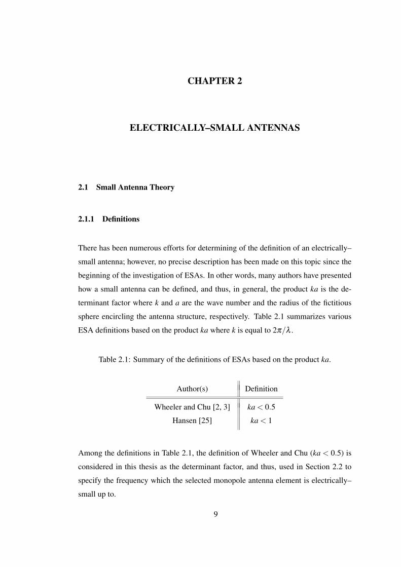
reactive power. He considered a capacitor and an inductor that occupy same volume
as small antennas, which also correspond to electric and magnetic dipoles, respec-
tively [2, 26]. The equivalent circuit models for the electric and magnetic dipole
antennas are derived in [2] and shown in Figure 2.1.
Figure 2.1: The equivalent circuit representation of Wheeler’s antennas: (a) Electricdipole. (b) Magnetic dipole. [1, 2]
The values of the lumped circuit elements shown in Figure 2.1 can be summarized in
Equation 2.1 and Equation 2.2 as [1, 27]:
C =ε0kaA
band L =
µ0n2Akbb
(2.1)
Gel =1
6πη0
[kaA
(λ/2π)2
]2
and Rmag = 20[
nA(λ/2π)2
]2
(2.2)
where Gel and Rmag are the radiation shunt conductance and radiation series resis-
10

tance, respectively. η0, ε0 and µ0 are the wave impedance, permittivity of the free
space and permeability of the free space, respectively. Here, the terms ka and kb
named as shape factors are used to consider the effective area of the capacitor and
effective length of inductor. By this way, the external electric and magnetic fiels are
taken into account [1]. Also, n, b and A are the number of turns in the inductor
(solenoid), the height of the cylinder and the area (πa2, with a being the radius of the
cylinder), respectively.
In addition to Wheeler, Chu also investigated the fundamental limitations of ESAs
as well. In his work, he studied the analysis of a vertically–polarized dipole antenna
to find the radiated field outside a hypothetical sphere of radius a using the spherical
mode expansions [4, 3]. The expansion for the radiated field expression is the sum of
all spherical modes, each corresponding to an L–C network in the equivalent circuit
representation. Using the wave impedances for TE and TM modes, equivalent circuit
model and the radiation quality factor of the antenna (Qrad) can be found. A detailed
derivation of these quantities is given in [1]. The minimum Q–factor (Qrad) can be
obtained according to the Chu’s analysis is given as [3]:
Qchu =1+2(ka)2
(ka)3[1+(ka)2](2.3)
Using the wave impedance formulations presented in [1, 3, 28], the equivalent circuits
for TM10 and TE10 modes can be given in Figure 2.2. The terms ZTM10r and ZTE10
r
are the wave impedances of outward radiating TM10 and TE10 modes, respectively.
The term r is the largest radius of a hypothetical sphere enclosing the antenna. The
equivalent circuit representation and the wave impedances are the essential factors
when finding the minimum Q–factor (Qchu) given in Equation 2.3.
Figure 2.2: The equivalent circuit model for (a) TM10 mode and (b) TE10 mode [1, 3].
11
Later on, McLean worked on the radiation quality factor (Qrad) and enhanced the
result which will be presented in Section 2.2.2. Obtaining an expression for Qrad has
been an active discussion topic among many researchers; however, it is not possible to
discuss all of the work in any further detail in this thesis. Minimum Q–limit derived
by various authors are summarized in Table 2.2.
Table 2.2: Minimum Qrad expressions derived by various authors.
Author(s) Minimum Qrad
Wheeler [26] 1(ka)3
Chu [3] 1+2(ka)2
(ka)3[1+(ka)2]
McLean [29] 1ka
+1
(ka)3
Hansen and Collin [30] 1√2ka
+1
(ka)3
Gustaffson [31] 1.5(ka)3
Geyi [32] 1ka
+1
2(ka)3
2.2 Monopole Antennas
The most extensively used antennas in wireless communication systems are dipole
and monopole antennas. Monopole antennas are generally preferred for portable de-
vices due to their simple structure, accessibility and good radiation characteristics.
These antenna characteristics are strongly dependent upon the size of the ground
plane and the electrical length that is related to frequency of operation. Generally,
dipole and monopole antennas are employed as λ/2 and λ/4 elements, respectively;
however, that is not always the case. Hence, these antennas can be used as electri-
cally short elements whose electrical lengths are much less than a wavelength. Ideally,
monopole antennas are built on an infinite ground plane; however, in practice, such
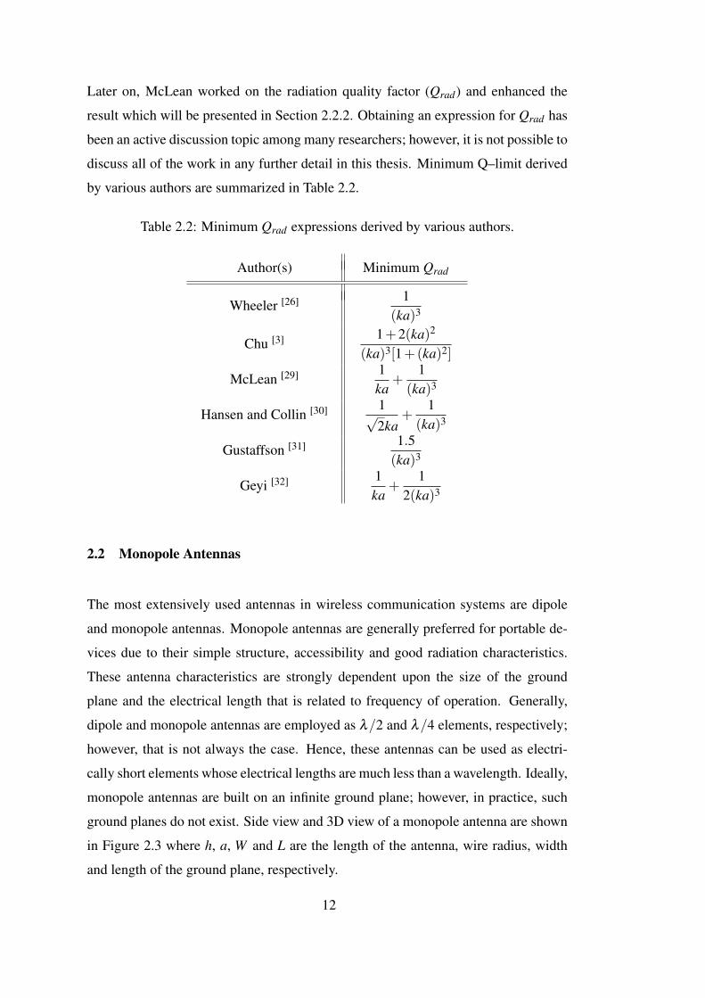
ground planes do not exist. Side view and 3D view of a monopole antenna are shown
in Figure 2.3 where h, a, W and L are the length of the antenna, wire radius, width
and length of the ground plane, respectively.
12
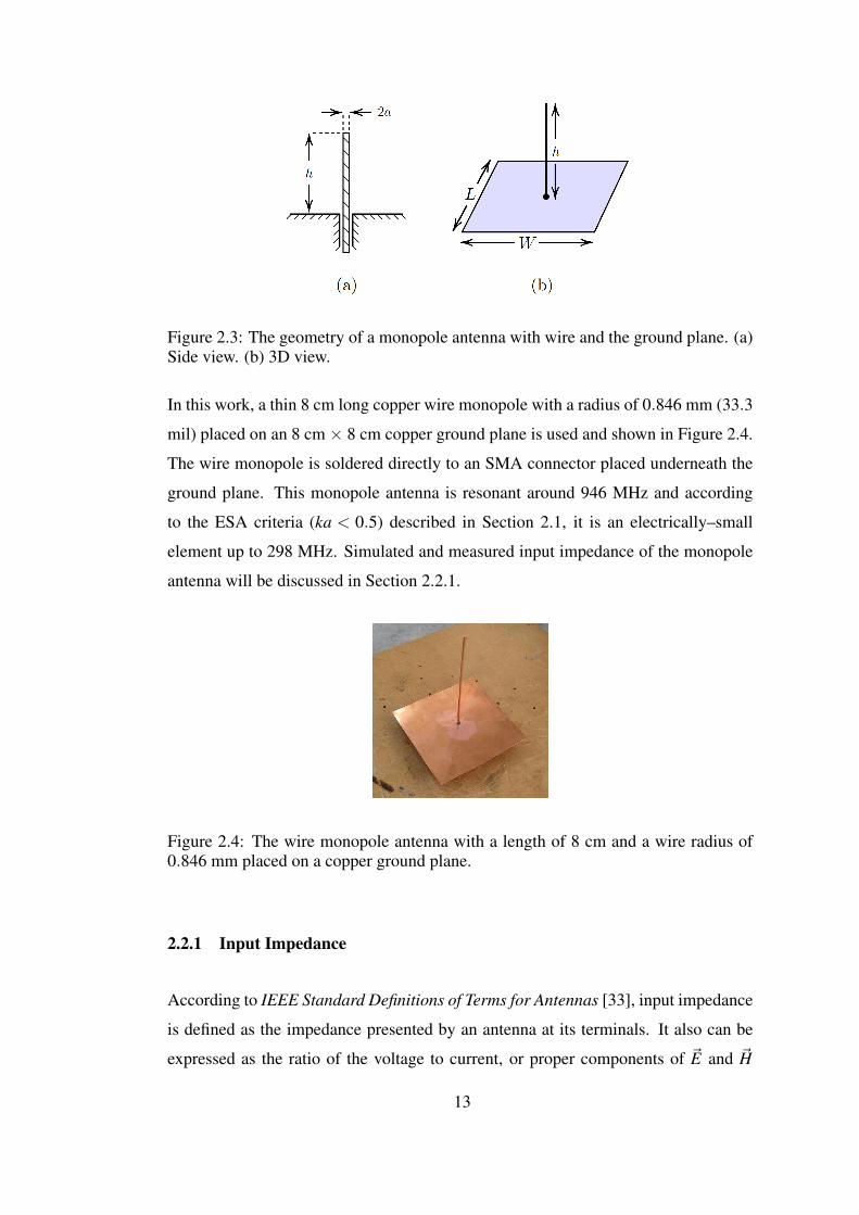
Figure 2.3: The geometry of a monopole antenna with wire and the ground plane. (a)Side view. (b) 3D view.
In this work, a thin 8 cm long copper wire monopole with a radius of 0.846 mm (33.3
mil) placed on an 8 cm × 8 cm copper ground plane is used and shown in Figure 2.4.
The wire monopole is soldered directly to an SMA connector placed underneath the
ground plane. This monopole antenna is resonant around 946 MHz and according
to the ESA criteria (ka < 0.5) described in Section 2.1, it is an electrically–small
element up to 298 MHz. Simulated and measured input impedance of the monopole
antenna will be discussed in Section 2.2.1.
Figure 2.4: The wire monopole antenna with a length of 8 cm and a wire radius of0.846 mm placed on a copper ground plane.
2.2.1 Input Impedance
According to IEEE Standard Definitions of Terms for Antennas [33], input impedance
is defined as the impedance presented by an antenna at its terminals. It also can be
expressed as the ratio of the voltage to current, or proper components of ~E and ~H
13

fields at the terminals of the antenna. The antenna input impedance is a complex
number, thus one can write it as:
ZA = RA + jXA (2.4)
where RA and XA are the real (resistive) and imaginary (reactive) parts of the antenna
input impedance. The resistive part of the input impedance consists of the radiation
resistance (Rr) and loss resistance (RL). In circuit theory a resistance generally corre-
sponds to a loss, for antennas however, power radiated from the antenna is related to
the radiation resistance.
The real part of the antenna input impedance gives an important information about the
power radiated from the antenna or received by the antenna. On the other hand, the
imaginary part of the antenna input impedance corresponds to the power that is stored
in the near–field region of the antenna, i.e., it is non–radiated. In this respect, design of
an antenna for optimal radiation characteristics is contingent upon the knowledge of
antenna impedance behavior. The antenna input impedance is a function of frequency,
and hence, antennas can only be matched in a certain finite bandwidth. In Figure 2.5,
the equivalent circuits involving the real and imaginary parts of input impedance for
transmitting and receiving antennas are shown. For an antenna in transmitting mode,
a generator having an internal impedance of ZG is connected to the input terminals
of the antenna. For an antenna in receiving mode, an arbitrary load of ZL is con-
nected to the input terminals. The electromagnetic wave incident to the antenna may
be modeled by a voltage generator of VG. In both cases, the antenna impedance is
characterized by the resistive part (Rr and RL) and the imaginary part (XA).
To design an impedance matching network for an antenna, first, the antenna input
impedance must be known. Electrically–small antennas are characterized by a large
reactance (XA) and a small resistance (RA). Due to this reason, a small portion of the
power accepted by the antenna terminals will be radiated in the far–field region, and
thus, most of the power will be stored in the near–field region. Having a large reactive
part in input impedance compared to the resistive part asserts the fact that an ESA has
14
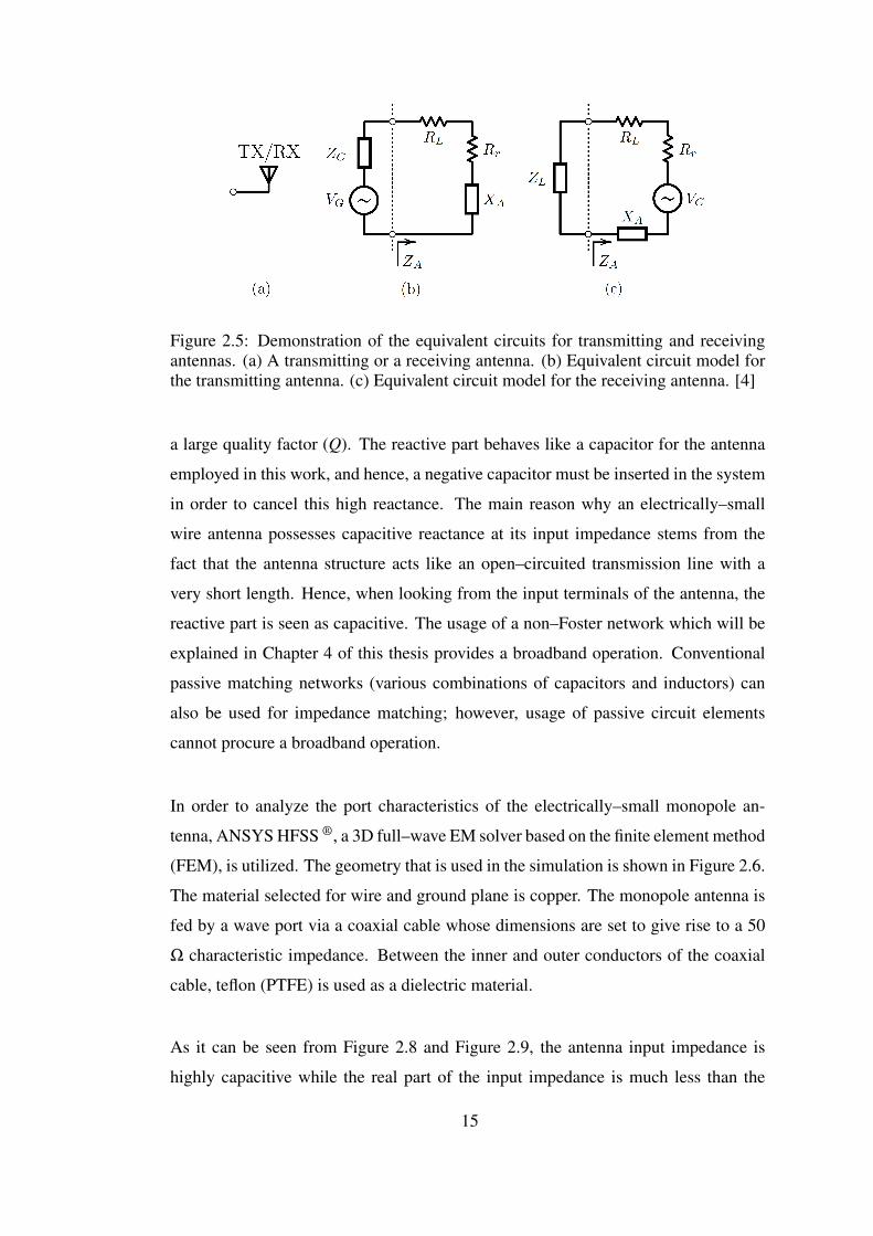
Figure 2.5: Demonstration of the equivalent circuits for transmitting and receivingantennas. (a) A transmitting or a receiving antenna. (b) Equivalent circuit model forthe transmitting antenna. (c) Equivalent circuit model for the receiving antenna. [4]
a large quality factor (Q). The reactive part behaves like a capacitor for the antenna
employed in this work, and hence, a negative capacitor must be inserted in the system
in order to cancel this high reactance. The main reason why an electrically–small
wire antenna possesses capacitive reactance at its input impedance stems from the
fact that the antenna structure acts like an open–circuited transmission line with a
very short length. Hence, when looking from the input terminals of the antenna, the
reactive part is seen as capacitive. The usage of a non–Foster network which will be
explained in Chapter 4 of this thesis provides a broadband operation. Conventional
passive matching networks (various combinations of capacitors and inductors) can
also be used for impedance matching; however, usage of passive circuit elements
cannot procure a broadband operation.
In order to analyze the port characteristics of the electrically–small monopole an-
tenna, ANSYS HFSS ®, a 3D full–wave EM solver based on the finite element method
(FEM), is utilized. The geometry that is used in the simulation is shown in Figure 2.6.
The material selected for wire and ground plane is copper. The monopole antenna is
fed by a wave port via a coaxial cable whose dimensions are set to give rise to a 50
Ω characteristic impedance. Between the inner and outer conductors of the coaxial
cable, teflon (PTFE) is used as a dielectric material.
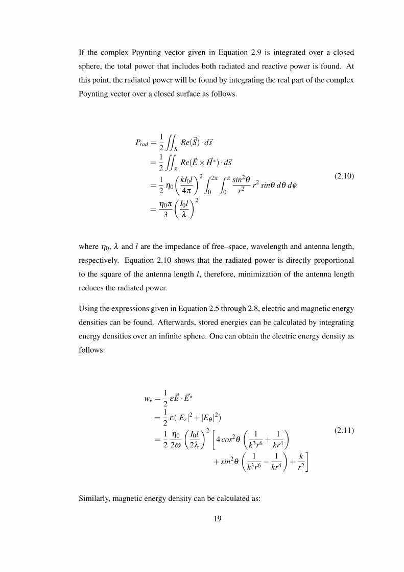
As it can be seen from Figure 2.8 and Figure 2.9, the antenna input impedance is
highly capacitive while the real part of the input impedance is much less than the
15
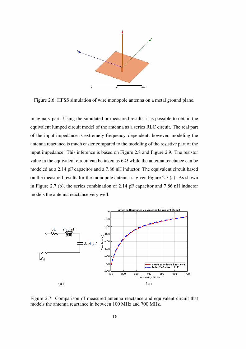
Figure 2.6: HFSS simulation of wire monopole antenna on a metal ground plane.
imaginary part. Using the simulated or measured results, it is possible to obtain the
equivalent lumped circuit model of the antenna as a series RLC circuit. The real part
of the input impedance is extremely frequency–dependent; however, modeling the
antenna reactance is much easier compared to the modeling of the resistive part of the
input impedance. This inference is based on Figure 2.8 and Figure 2.9. The resistor
value in the equivalent circuit can be taken as 6 Ω while the antenna reactance can be
modeled as a 2.14 pF capacitor and a 7.86 nH inductor. The equivalent circuit based
on the measured results for the monopole antenna is given Figure 2.7 (a). As shown
in Figure 2.7 (b), the series combination of 2.14 pF capacitor and 7.86 nH inductor
models the antenna reactance very well.
Figure 2.7: Comparison of measured antenna reactance and equivalent circuit thatmodels the antenna reactance in between 100 MHz and 700 MHz.
16
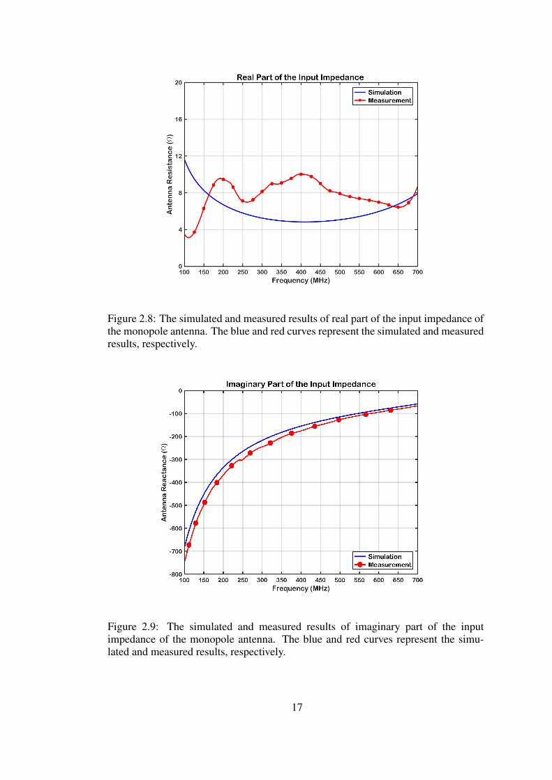
Figure 2.8: The simulated and measured results of real part of the input impedance ofthe monopole antenna. The blue and red curves represent the simulated and measuredresults, respectively.
Figure 2.9: The simulated and measured results of imaginary part of the inputimpedance of the monopole antenna. The blue and red curves represent the simu-lated and measured results, respectively.
17

2.2.2 Stored Energies, Radiation Quality Factor and Bandwidth
As mentioned in Section 2.2.1, electrically–small antennas are the antennas whose
reactive (imaginary) part of input impedance is much greater than resistive (real) part.
This is simply because of the fact that the geometrical dimensions of ESAs are very
small compared to the wavelength of operation. In this respect, most of the power is
stored in the near–field region whereas a small amount of power is radiated from the
antenna. This section is based on McLean’s work on the exact derivation of radiation
quality factor (Q) [29]. First, the stored energies in the near–field region are derived.
Then, the relationship between stored energies, radiation quality factor and bandwidth
is addressed.
The radiation characteristics of a wire antenna can be investigated solving the vector
potential equation and Maxwell’s equations. Consider a z–directed dipole antenna of
length l and having a current of I0. The electric and magnetic fields due to this dipole
antenna can be written as [4]:
Er =η0I0l2π
cosθe− jkr
r2
[1+
1jkr
](2.5)
Eθ =jk
4πη0 I0 l sinθ
e− jkr
r
[1+
1jkr− 1
(kr)2
](2.6)
Eφ = Hr = Hθ = 0 (2.7)
Hφ =jk
4πI0 l sinθ
e− jkr
r
[1+
1jkr
](2.8)
where η0, λ and I0 are the impedance of free–space, wavelength and antenna current,
respectively. The equations given in 2.5 – 2.8 include both far–field and near–field
components, and hence, to be able to calculate the radiated power, far–field compo-
nents must be taken into account. The complex Poynting vector can be written as:
~S =12~E× ~H∗
=12(~arEθ H∗φ −~aθ ErH∗θ )
(2.9)
18
If the complex Poynting vector given in Equation 2.9 is integrated over a closed
sphere, the total power that includes both radiated and reactive power is found. At
this point, the radiated power will be found by integrating the real part of the complex
Poynting vector over a closed surface as follows.
Prad =12
∫∫S
Re(~S) ·d~s
=12
∫∫S
Re(~E× ~H∗) ·d~s
=12
η0
(kI0l4π
)2 ∫ 2π
0
∫π
0
sin2θ
r2 r2 sinθ dθ dφ
=η0π
3
(I0lλ
)2
(2.10)
where η0, λ and l are the impedance of free–space, wavelength and antenna length,
respectively. Equation 2.10 shows that the radiated power is directly proportional
to the square of the antenna length l, therefore, minimization of the antenna length
reduces the radiated power.
Using the expressions given in Equation 2.5 through 2.8, electric and magnetic energy
densities can be found. Afterwards, stored energies can be calculated by integrating
energy densities over an infinite sphere. One can obtain the electric energy density as
follows:
we =12
ε~E · ~E∗
=12
ε(|Er|2 + |Eθ |2)
=12
η0
2ω
(I0l2λ
)2 [4cos2
θ
(1
k3r6 +1
kr4
)+ sin2
θ
(1
k3r6 −1
kr4
)+
kr2
](2.11)
Similarly, magnetic energy density can be calculated as:
19
wm =12
µ~H · ~H∗
=12
µ(|Hφ |2)
=12
µ
(I0l2λ
)2
sin2θ
(1r2 +
1k2r4
) (2.12)
To be able to find the nonpropagating (stored) electric and magnetic energy densities,
first, the energy densities related to the propagating wave must be found. The electric
and magnetic energy densities associated with the traveling electromagnetic wave
can be calculated using far–field expressions that originate the radiated power. Using
far–field terms in equations 2.5, 2.6 and 2.8, similar steps can be applied to find the
electric and magnetic energy densities associated with the traveling wave as follows:
wrade =
12
η20 ε
(I0l2λ
)2
sin2θ
1r2
(2.13)
wradm =
12
µ
(I0l2λ
)2
sin2θ
1r2
(2.14)
Defining the stored electric and magnetic energy densities as w′e and w
′m, respectively,
they can be written as:
w′e = we−wrad
e
=η0
2ωµ
(I0l2λ
)2 [4cos2
θ
(1
k3r6 +1
kr4
)+ sin2
θ
(1
k3r6 −1
kr4
)] (2.15)
w′m = wm−wrad
m =12
µ
(I0l2λ
)2
sin2θ
1r4
(2.16)
The stored electric and magnetic energies can be calculated as:
20

W′e =
∫ 2π
0
∫π
0
∫∞
aw′e r2 sinθ dr dθ dφ (2.17)
W′m =
∫ 2π
0
∫π
0
∫∞
aw′m r2 sinθ dr dθ dφ (2.18)
where a is the radius of the sphere that circumscribes the antenna. Therefore, the
stored electric energy can be written as:
W′e =
4πη0
3ω
(I0l2λ
)2 [ 1ka
+1
(ka)3
](2.19)
Similarly, the stored magnetic energy can be written as:
W′m =
η0ω
12π(I0l)2 1
ka(2.20)
The radiation quality factor (Q) for an antenna is defined as:
Q =
2ω W
′e
Pradif W
′e > W
′m
2ω W′m
Pradif W
′m > W
′e
(2.21)
For electrically–small antennas, the first condition given in Equation 2.21 is valid due
to the fact that stored electric energy is greater than stored magnetic energy. Hence,
one can write the radiation quality factor (Q) by using equations 2.10, 2.19 and 2.21
as [29]:
Q =2ωW
′m
Prad=
1ka
+1
(ka)3 (2.22)
As it can be seen from Equation 2.22, antenna size, operation frequency and radiation
quality factor are related. As presented in Table 2.2, the reason why different authors
21

and researchers come up with miscellaneous radiation quality factors stems from the
fact that they have used various assumptions which express the radiation quality factor
differently.
Another important parameter is bandwidth which is also related to radiation quality
factor. The fractional bandwidth is a figure of merit that is used to have an idea about
how wideband the antenna is, and given as [34]:
FBW =∆ ffc
=1Q
(2.23)
where ∆ f and fc are 3–dB bandwidth and the center frequency. As it can be seen from
equations 2.22 and 2.23, there is a trade–off between the bandwidth and antenna size.
Once the antenna size is decreased for a given frequency, the radiation quality factor
increases. Hence, an increase in the Q–factor decreases the fractional bandwidth.
Since lower Q–factor means that the antenna operates in a wider band, equations 2.22
and 2.23 impose an important limitation on the antenna performance as well as the
design.
22
CHAPTER 3
DESIGN AND IMPLEMENTATION OF A MONOPOLE
ANTENNA USING REACTIVE LOADING
3.1 Introduction to Reactive Loading
Wire antennas are one of the most all–round, handy and the least expensive an-
tennas for many applications, and thus, have been still utilized widely. Owing to
this reason and a demand for wideband antenna operation, for couple decades, re-
searchers have been working on reactive loading of wire antennas. A growing in-
terest on this topic has ascertained many antenna designs, and they are found place
in literature [22, 23, 24, 35]. Reactive loading of the antennas can improve the an-
tenna radiation characteristics and some important parameters such as antenna gain
and VSWR. Nowadays, many commercial simulation tools such as CST Microwave
Studio®, AWR Microwave Office® and ANSYS HFSS® can be used to analyze lots
of various antenna structures by means of well–known numerical techniques, i.e., the
method of moments (MoM), the finite integration technique (FIT), the finite–element
method (FEM) or the finite-difference time–domain (FDTD). On the other hand, to
synthesize an antenna with some predetermined characteristics over a wide band is
a difficult process, and thus, cannot be done only by means of the aforementioned
numerical methods. In this respect, for such a synthesis purpose, optimization al-
gorithms must be implemented and used together with numerical methods. In this
thesis, for example, a genetic algorithm (GA) and MoM are utilized as the optimiza-
tion tool and the numerical method to characterize the electromagnetic performance,
respectively.
23

In reactive loading, passive lumped circuit elements (R, L and C) are placed on the
antenna in order to adjust the current distribution over the wire so that the antenna
performance and radiation characteristics can be enhanced [24]. The optimization
process is basically to try to find the best values for lumped elements of load(s) placed
on the antenna according to the desired antenna features. In general, it is aimed to
improve both the VSWR (or return loss, S11) and the antenna gain. An example
demonstration of antenna loading is shown in Figure 3.1 in which the number of loads
and lumped element types are provided arbitrarily. In other words, combinations of
R, L and C do not necessarily have to be as shown in the figure. The optimization
algorithm will produce different combinations of loads and their values in accordance
with the constraints.
Figure 3.1: An example demonstration of a loaded wire monopole antenna with threedifferent load sections with h1, h2 and h3 being the heights of each load, and a is thewire radius.
Due to the fact that it is very difficult to meet the antenna parameter specifications
only by using reactive loads on the wire, an additional matching circuit comprised of
transformers and ladder networks is connected to the input terminals of the antenna.
In the optimization phase, the values of load components and the values of the circuit
components in the external matching network are computed simultaneously. The
external matching network to be connected to the antenna is shown in Figure 3.2.
For the synthesis of reactively–loaded antennas, genetic algorithms (GA) are exten-
sively utilized. Genetic algorithms are widely–used, robust and efficient search algo-
24
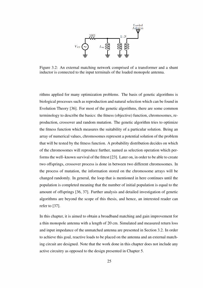
Figure 3.2: An external matching network comprised of a transformer and a shuntinductor is connected to the input terminals of the loaded monopole antenna.
rithms applied for many optimization problems. The basis of genetic algorithms is
biological processes such as reproduction and natural selection which can be found in
Evolution Theory [36]. For most of the genetic algorithms, there are some common
terminology to describe the basics: the fitness (objective) function, chromosomes, re-
production, crossover and random mutation. The genetic algorithm tries to optimize
the fitness function which measures the suitability of a particular solution. Being an
array of numerical values, chromosomes represent a potential solution of the problem
that will be tested by the fitness function. A probability distribution decides on which
of the chromosomes will reproduce further, named as selection operation which per-
forms the well–known survival of the fittest [23]. Later on, in order to be able to create
two offsprings, crossover process is done in between two different chromosomes. In
the process of mutation, the information stored on the chromosome arrays will be
changed randomly. In general, the loop that is mentioned in here continues until the
population is completed meaning that the number of initial population is equal to the
amount of offsprings [36, 37]. Further analysis and detailed investigation of genetic
algorithms are beyond the scope of this thesis, and hence, an interested reader can
refer to [37].
In this chapter, it is aimed to obtain a broadband matching and gain improvement for
a thin monopole antenna with a length of 20 cm. Simulated and measured return loss
and input impedance of the unmatched antenna are presented in Section 3.2. In order
to achieve this goal, reactive loads to be placed on the antenna and an external match-
ing circuit are designed. Note that the work done in this chapter does not include any
active circuitry as opposed to the design presented in Chapter 5.
25

3.2 The Thin Monopole Antenna
In this section, the input impedance and return loss characteristics of the unloaded
monopole antenna are demonstrated. Furthermore, the reactive loading for a thin
monopole antenna with a height of 20 cm is presented. The monopole antenna has
been cut from a thin copper sheet, and thus, the thickness of the antenna is very small,
and the width of the thin monopole antenna is 1 cm. Also, a 50 cm by 50 cm square
ground plane has been used. Simulated results for input impedance and return loss for
this unloaded monopole antenna is obtained using ANSYS HFSS®. In the simulation
software, the material of the thin monopole antenna and ground plane is selected as
copper. The monopole antenna is fed by a wave port via a coaxial cable with the
dimensions set up for 50Ω characteristic impedance. Figure 3.3 shows the simulated
and measured return loss of the unloaded monopole antenna. It is observed from the
figure that the measured return loss agrees very well with the simulated results. The
antenna resonance frequency is nearly 350 MHz with a 6–dB bandwidth of 65 MHz.
Figure 3.3: Simulated and measured return loss of the unloaded monopole antenna.The solid red line and the blue dashed line represent measured and simulated |S11|data, respectively.
In addition to the return loss data, measured input impedance characteristics of the
unloaded thin monopole antenna are also investigated and shown in Figure 3.4. Due
to the fact that the resonant frequency of the thin monopole antenna is around 340
26

MHz, it can be seen from Figure 3.4 that the reactive part of the input impedance is
not too large in the vicinity of this frequency as expected. However, the real part of
the input impedance gets close to very small numbers as frequency decreases which
may aggravate the impedance matching at low frequencies.
Figure 3.4: Measured input impedance of the unloaded monopole antenna. The solidred line and the blue dashed line represent imaginary and real parts of the inputimpedance, respectively.
3.3 Design of the Loaded Antenna and Matching Network
In the design phase of reactively–loaded monopole antennas and external matching
networks, a MATLAB® program written by Prof. Sencer Koç at METU has been
utilized. With the utilization of this program, it is possible to analyze wire antennas
using method of moments (MoM) and optimize the load positions and the values of
loads and lumped components in the external matching network. Prior to running the
program, the antenna length and wire radius, frequency of operation, design goals,
minimum and maximum bounds for lumped component values, and number of seg-
ments needed for MoM analysis can be entered as input variables. Prior to performing
EM analysis, the antenna is divided into a number of segments for which the basis
(expansion) functions and antenna currents at each node are calculated. Hence, elec-
tromagnetic analysis of the wire antenna is performed using method of moments in
which the MoM impedance matrix (Zmn) and its inverse (Ymn) are calculated by ap-
27
plying this technique to the electric–field integral equation (EFIE). For the unloaded
wire monopole antenna, this MoM impedance matrix is evaluated in all frequencies
which are entered prior to running the code.
Following the electromagnetic analysis of the straight–wire monopole antenna, op-
timization algorithms are used to evaluate the reactive load values, lumped compo-
nents and load position. Within the program, there are three different optimization
algorithms: a genetic algorithm coded by Prof. Sencer Koç and two built–in opti-
mizer functions provided by MATLAB®. These functions are fmincon and fminimax
that the former attempts to minimize a function subject to given constraints, and the
latter tries to minimize the largest value of a multivariable function. Therefore, it is
possible to use these three algorithms to find the load values and positions.
In the design of the reactive loading and the external matching circuit by optimization
algorithms, the following objective function has been used [22].
F =−N f
∑k=1
u[
V SWR( fk), V SWR D( fk)]−
N f
∑k=1
u[
G DS ( fk), GS( fk)
](3.1)
where u(x,y) = |x− y|2 if x > y, and zero otherwise. In Equation 3.1, the superscript
D and the subscript S denote desired value and system gain, respectively [22]. The
definition of the system gain GS can be expressed as:
GS = 10 log[(1−|Γ|2)GA
](3.2)
where GA and Γ are the antenna gain and reflection coefficient of the matching net-
work, respectively. As mentioned in Section 3.1, a reactive load can consist of a
resistor, an inductor, a capacitor or a combination of these three elements. Also, the
external matching is comprised of a transformer and a shunt inductor. Therefore, it
is the designer’s choice which of these elements are included in the optimization al-
gorithm. Hence, in this work, both reactive load values, load positions and external
matching elements are the optimization parameters. With the use of genetic algo-
rithm in the MATLAB® code, it is aimed to minimize the objective (fitness) function
28
given in Equation 3.1. Thus, attaining the minimum value of the fitness function F
corresponds to the fact that all design specifications are met over the specified band-
width. Basicly, the genetic algorithm starts with a randomly generated chromosomes
which are stored in a matrix named as the initial population. In fact, a chromo-
some is a numerical value (or a bit–string) that is a potential solution candidate to
the objective function [38]. Each chromosome in this matrix along with the inverse
impedance matrix (Ymn) and the MoM excitation vector (Vm) are evaluated by the
objective function1. Then, the algorithm selects some of the chromosomes for re-
production, crossover and mutation. Description of all stages of GA are beyond the
scope of this thesis, and thus, an interested reader can refer to [37, 38]. As a result of
these stages, a new generation of chromosomes are created and subject to be tested by
the objective function once again. This process continues until the genetic algorithm
finds a minimum value of the objective function. However, the process may stall be-
fore finding the minimum value of F due to the fact that prescribed design goals can
be difficult for the genetic algorithm to achieve.
The design parameters are selected as given in Table 3.1. The number of loads is
chosen as one because the antenna length is physically small. Also, the frequency
step and the number of segments are chosen as 5 MHz and 61, respectively.
Table 3.1: The design parameters of the reactive loading and matching circuit enteredin the genetic algorithm code in MATLAB®.
Parameter Value
Monopole length 0.2 m
Wire radius 5 mm
Frequency range 150 – 500 MHz
Number of segments 61
Desired gain −10 dB
Desired VSWR 3 (max)
1 Given an equation in the form of LIφ = u where LI , φ and u are integral operator, response function andexcitation function, respectively, an integral equation can be transformed into a matrix equation using method ofmoments. This matrix equation can be expressed as [Zmn][In] = [Vm], and its inverse is [In] = [Ymn][Vm] where[Ymn] = [Zmn]
−1 and [Zmn] is named as impedance (moment) matrix [4].
29
3.4 Simulated and Measured Results
In this section, three design examples are presented. Table 3.1 summarizes the de-
sign goals entered into the MATLAB® program. During the optimization process,
the genetic algorithm coded in the program has been used to find solutions for the
desired antenna parameters. After the optimization process is completed, values of
the components in the reactive load and external matching network can be tuned in
the optimization program. It is necessary especially for the transformer due to the
fact that the optimizer program finds a transformer with an impedance transformation
ratio that may not be available in the market. The calculated and tuned values of three
reactive loading designs are given in Table 3.2.
Table 3.2: The calculated values of the lumped components of reactive loads andexternal matching circuit.
Parameter Design #1 Design #2 Design #3
R1 315Ω 200Ω 330Ω
C1 N/A 1.2 pF N/A
L1 270 nH 150 nH 150 nH
Load Height, h1 5 cm 3 cm 5 cm
N 2 3 2
Lm 390 nH 390 nH 200 nH
Surface–mount mini wideband transformers with turn ratios of 1:2 and 1:3 that of-
fers quite good insertion losses over wide bandwidths are obtained from Coilcraft®.
Transformers with turn ratios of 1:2 and 1:3 have 3–dB bandwidths of 0.2 MHz – 500
MHz and 0.3 MHz – 900 MHz, respectively [39]. The monopole antennas are fabri-
cated by soldering two different copper sheets together, and in between these sheets,
the reactive loads are inserted. Fabricated loaded monopole antenna is connected to
an SMA connector, and the external matching network is connected to the SMA con-
nector under the ground plane. The measured and simulated return loss and VSWR
data for Design #1 and Design #2 are given in Figure 3.5 and Figure 3.6, respectively.
The solid red line and blue dashed line represent the measured and simulated data,
30

respectively. For Design #1, it is observed that 6–dB matching is achieved in between
156 MHz and 306 MHz, corresponding to a bandwidth of 150 MHz. Similarly, for
Design #2, it is observed that 6–dB matching is achieved in between 346 MHz and
553 MHz, corresponding to a bandwidth of 207 MHz. Additionally, the simulated
data agrees with the measured data inside and the vicinity of the band in which the
monopole antenna is matched.
Figure 3.5: Simulated and measured return loss (S11) and VSWR data for Design #1.The solid red and blue dashed lines correspond to measured and simulated data.
Having presented Design #1 and Design #2, the values of Design #3 is initially ob-
tained as given in Table 3.2. In this case, the load height h1 is evaluated as 5 cm
which later is swept for different values such as: 5 cm, 7 cm, 10 cm, 13 cm and 15
cm in order to observe the effect of load position on the antenna. Measured return
loss (S11) data of the loaded antenna for various load positions is shown in Figure
3.7. Compared to Design #1 and #2, the values of Design #3 are tuned for better
return loss values. An increase in the load position (h1) causes the return loss data to
shift to the higher frequencies; however, this does not increase the bandwidth which
is found nearly as 290 MHz. Among these three reactive load designs, it is observed
that Design #3 has provided better impedance match over 100 MHz and 600 MHz
band.
31
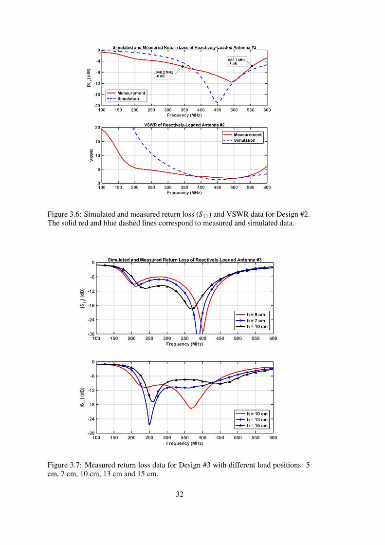
Figure 3.6: Simulated and measured return loss (S11) and VSWR data for Design #2.The solid red and blue dashed lines correspond to measured and simulated data.
Figure 3.7: Measured return loss data for Design #3 with different load positions: 5cm, 7 cm, 10 cm, 13 cm and 15 cm.
32
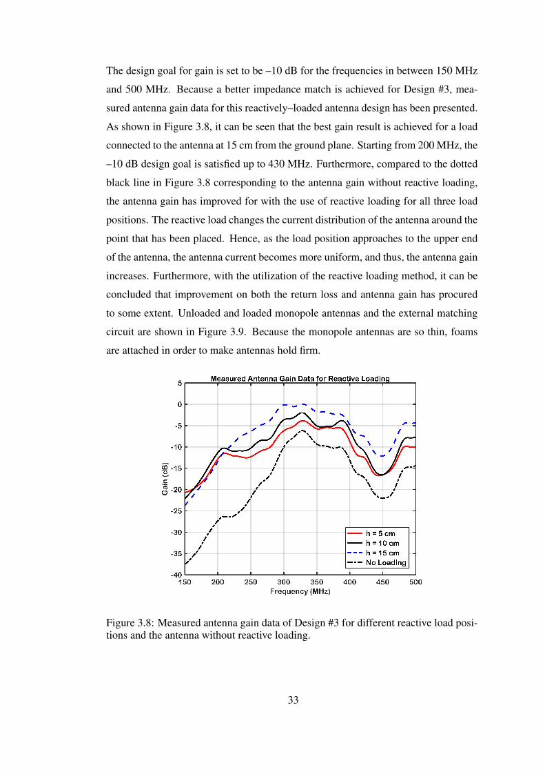
The design goal for gain is set to be –10 dB for the frequencies in between 150 MHz
and 500 MHz. Because a better impedance match is achieved for Design #3, mea-
sured antenna gain data for this reactively–loaded antenna design has been presented.
As shown in Figure 3.8, it can be seen that the best gain result is achieved for a load
connected to the antenna at 15 cm from the ground plane. Starting from 200 MHz, the
–10 dB design goal is satisfied up to 430 MHz. Furthermore, compared to the dotted
black line in Figure 3.8 corresponding to the antenna gain without reactive loading,
the antenna gain has improved for with the use of reactive loading for all three load
positions. The reactive load changes the current distribution of the antenna around the
point that has been placed. Hence, as the load position approaches to the upper end
of the antenna, the antenna current becomes more uniform, and thus, the antenna gain
increases. Furthermore, with the utilization of the reactive loading method, it can be
concluded that improvement on both the return loss and antenna gain has procured
to some extent. Unloaded and loaded monopole antennas and the external matching
circuit are shown in Figure 3.9. Because the monopole antennas are so thin, foams
are attached in order to make antennas hold firm.
Figure 3.8: Measured antenna gain data of Design #3 for different reactive load posi-tions and the antenna without reactive loading.
33
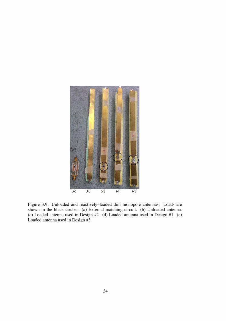
Figure 3.9: Unloaded and reactively–loaded thin monopole antennas. Loads areshown in the black circles. (a) External matching circuit. (b) Unloaded antenna.(c) Loaded antenna used in Design #2. (d) Loaded antenna used in Design #1. (e)Loaded antenna used in Design #3.
34
CHAPTER 4
NON–FOSTER MATCHING
4.1 Passive and Active Impedance Matching
4.1.1 Foster Reactance Theorem
Before delving into the theory of non–Foster impedances and non–Foster circuits,
Foster impedances and Foster reactance theorem should be addressed. Foster reac-
tance theorem, introduced by Ronald M. Foster in 1924, states that the derivatives
of reactance and susceptance functions with respect to frequency are greater than
zero [40]. In other words, the slopes of reactance and susceptance functions versus
frequency are positive. Hence, for passive and lossless networks, the reactance and
susceptance functions increase monotonically with frequency which can be written
as follows:
∂X(ω)
∂ω> 0 and
∂B(ω)
∂ω> 0 (4.1)
where X(ω) and B(ω) are reactance and susceptance functions, respectively. Any
lossless passive circuit element obeys this rule is named as a Foster element. In
fact, this Foster element corresponds to a conventional passive circuit element which
is either a capacitor or an inductor. Generally, impedance matching networks are
constructed using these conventional capacitor and inductor elements, and thus, they
are called conventional passive matching networks. In Figure 4.1, reactance curves
of conventional passive lossless inductor and capacitor are given.
35
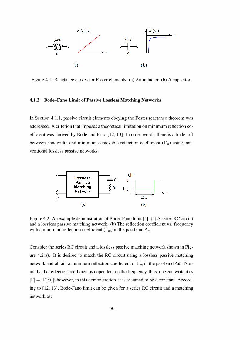
Figure 4.1: Reactance curves for Foster elements: (a) An inductor. (b) A capacitor.
4.1.2 Bode–Fano Limit of Passive Lossless Matching Networks
In Section 4.1.1, passive circuit elements obeying the Foster reactance theorem was
addressed. A criterion that imposes a theoretical limitation on minimum reflection co-
efficient was derived by Bode and Fano [12, 13]. In order words, there is a trade–off
between bandwidth and minimum achievable reflection coefficient (Γm) using con-
ventional lossless passive networks.
Figure 4.2: An example demonstration of Bode–Fano limit [5]. (a) A series RC circuitand a lossless passive matching network. (b) The reflection coefficient vs. frequencywith a minimum reflection coefficient (Γm) in the passband ∆ω .
Consider the series RC circuit and a lossless passive matching network shown in Fig-
ure 4.2(a). It is desired to match the RC circuit using a lossless passive matching
network and obtain a minimum reflection coefficient of Γm in the passband ∆ω . Nor-
mally, the reflection coefficient is dependent on the frequency, thus, one can write it as
|Γ|= |Γ(ω)|; however, in this demonstration, it is assumed to be a constant. Accord-
ing to [12, 13], Bode-Fano limit can be given for a series RC circuit and a matching
network as:
36

∫∞
0
1ω2 ln
1|Γ(ω)|
dω ≤ πRC (4.2)
In this case, the passband is finite, hence, ∆ω is in between ω1 and ω2. Therefore, the
integral in 4.2 can be arranged as:
∫∆ω
1ω2 ln
1|Γm|
dω =∫
ω2
ω1
1ω2 ln
1|Γm|
dω ≤ πRC (4.3)
Evaluating the integral in Equation 4.3, one can conclude the Bode–Fano limit as:
∆ω ln1
Γm≤ πω
2c RC (4.4)
where ωc is the geometric mean of the lower and upper bound of the passband. As it
can be seen from Equation 4.4, for a fixed R and C values, it is possible to achieve a
wider bandwidth only if the minimum reflection coefficient Γm is increased.
4.1.3 An Example of Passive Matching Using Lumped Circuit Elements
The Bode–Fano criterion for passive and lossless matching networks is presented in
Section 4.1.2. The main idea of this limitation is that it is only possible to obtain an
impedance match over a wider bandwidth if the minimum reflection coefficient (Γm)
over a passband of ∆ω increases. In this respect, in order to emphasize the need for
an active match over its passive counterparts, a numerical example is provided in this
section. In the design phase of the passive matching circuit, AWR Microwave Office®
commercial tool is utilized. The topology of the passive matching circuit is captured
by using iFilter Filter Synthesis tool of AWR Microwave Office® that is a quite useful
and handy tool for designing various filters such as lumped, microstrip, stripline, and
etc. Along with the selection of filter type, iFilter tool also offers different types of
filter response approximation functions such as Chebyshev, elliptic, Bessel, and many
others. The topology for the designed matching circuit in this section is of Chebyshev
37

type. However, in this section, the primary objective is not the design of a filter. The
reason why a filter design tool is used stems from the fact that this tool provides a cir-
cuit topology comprised of lumped circuit elements. In fact, this example of passive
matching is provided here in order to point out the Bode–Fano limit of lossless pas-
sive matching circuits. Once circuit topology is determined, optimization algorithms
are utilized to attain the desired matching condition over a specified bandwidth.
Consider the matching circuit shown in Figure 4.3 designed to match an 8 cm–long
electrically–small monopole antenna described in Section 2.2. This circuit topology
is obtained from iFilter tool of AWR Microwave Office®. In the design of the passive
matching network, the measured S–parameter values of the antenna has been used.
Note that other combinations of lumped circuit elements could also have been used
to generate a passive matching network.
Figure 4.3: An example passive matching network designed to match the electrically–small monopole antenna to 50Ω.
In order to match the ESA over a certain finite bandwidth, optimization algorithms
of AWR Microwave Office® have been used. The optimization process begins with
a very narrow band, and then, if the optimization goal (|S11| < −6 dB) is satisfied,
the bandwidth increased. This process helps the optimization algorithm find optimal
solutions easily due to the fact that the desired solution set is in the vicinity of the
previous solution.
Many optimization methods are offered by AWR Microwave Office® such as Simplex
Optimizer, Differential Evolution, Genetic Algorithm (GA, Gaussian mutation), and
Pointer – Robust Optimization. Among these methods, Simplex Optimizer (Local) is
found to be very successful while producing an optimal solution. Figure 4.4 shows
the simulated return loss and insertion loss results for the passive matching circuit
given in Figure 4.3 and the electrically–small antenna.
38
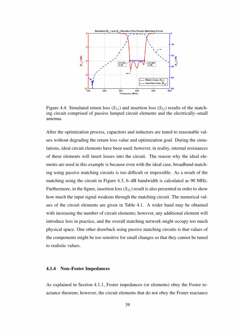
Figure 4.4: Simulated return loss (S11) and insertion loss (S21) results of the match-ing circuit comprised of passive lumped circuit elements and the electrically–smallantenna.
After the optimization process, capacitors and inductors are tuned to reasonable val-
ues without degrading the return loss value and optimization goal. During the simu-
lations, ideal circuit elements have been used; however, in reality, internal resistances
of these elements will insert losses into the circuit. The reason why the ideal ele-
ments are used in this example is because even with the ideal case, broadband match-
ing using passive matching circuits is too difficult or impossible. As a result of the
matching using the circuit in Figure 4.3, 6–dB bandwidth is calculated as 90 MHz.
Furthermore, in the figure, insertion loss (S21) result is also presented in order to show
how much the input signal weakens through the matching circuit. The numerical val-
ues of the circuit elements are given in Table 4.1. A wider band may be obtained
with increasing the number of circuit elements; however, any additional element will
introduce loss in practice, and the overall matching network might occupy too much
physical space. One other drawback using passive matching circuits is that values of
the components might be too sensitive for small changes so that they cannot be tuned
to realistic values.
4.1.4 Non–Foster Impedances
As explained in Section 4.1.1, Foster impedances (or elements) obey the Foster re-
actance theorem; however, the circuit elements that do not obey the Foster reactance
39
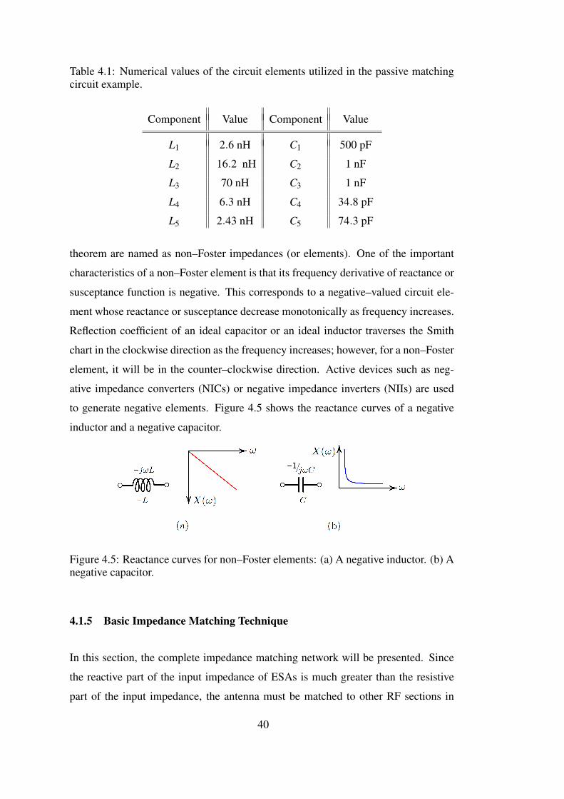
Table 4.1: Numerical values of the circuit elements utilized in the passive matchingcircuit example.
Component Value Component Value
L1 2.6 nH C1 500 pF
L2 16.2 nH C2 1 nF
L3 70 nH C3 1 nF
L4 6.3 nH C4 34.8 pF
L5 2.43 nH C5 74.3 pF
theorem are named as non–Foster impedances (or elements). One of the important
characteristics of a non–Foster element is that its frequency derivative of reactance or
susceptance function is negative. This corresponds to a negative–valued circuit ele-
ment whose reactance or susceptance decrease monotonically as frequency increases.
Reflection coefficient of an ideal capacitor or an ideal inductor traverses the Smith
chart in the clockwise direction as the frequency increases; however, for a non–Foster
element, it will be in the counter–clockwise direction. Active devices such as neg-
ative impedance converters (NICs) or negative impedance inverters (NIIs) are used
to generate negative elements. Figure 4.5 shows the reactance curves of a negative
inductor and a negative capacitor.
Figure 4.5: Reactance curves for non–Foster elements: (a) A negative inductor. (b) Anegative capacitor.
4.1.5 Basic Impedance Matching Technique
In this section, the complete impedance matching network will be presented. Since
the reactive part of the input impedance of ESAs is much greater than the resistive
part of the input impedance, the antenna must be matched to other RF sections in
40
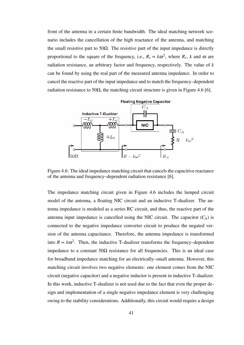
front of the antenna in a certain finite bandwidth. The ideal matching network sce-
nario includes the cancellation of the high reactance of the antenna, and matching
the small resistive part to 50Ω. The resistive part of the input impedance is directly
proportional to the square of the frequency, i.e., Rr ∝ kω2, where Rr, k and ω are
radiation resistance, an arbitrary factor and frequency, respectively. The value of k
can be found by using the real part of the measured antenna impedance. In order to
cancel the reactive part of the input impedance and to match the frequency–dependent
radiation resistance to 50Ω, the matching circuit structure is given in Figure 4.6 [6].
Figure 4.6: The ideal impedance matching circuit that cancels the capacitive reactanceof the antenna and frequency–dependent radiation resistance [6].
The impedance matching circuit given in Figure 4.6 includes the lumped circuit
model of the antenna, a floating NIC circuit and an inductive T–dualizer. The an-
tenna impedance is modeled as a series RC circuit, and thus, the reactive part of the
antenna input impedance is cancelled using the NIC circuit. The capacitor (CA) is
connected to the negative impedance converter circuit to produce the negated ver-
sion of the antenna capacitance. Therefore, the antenna impedance is transformed
into R ∝ kω2. Then, the inductive T–dualizer transforms the frequency–dependent
impedance to a constant 50Ω resistance for all frequencies. This is an ideal case
for broadband impedance matching for an electrically–small antenna. However, this
matching circuit involves two negative elements: one element comes from the NIC
circuit (negative capacitor) and a negative inductor is present in inductive T–dualizer.
In this work, inductive T–dualizer is not used due to the fact that even the proper de-
sign and implementation of a single negative impedance element is very challenging
owing to the stability considerations. Additionally, this circuit would require a design
41
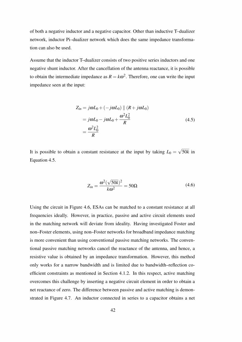
of both a negative inductor and a negative capacitor. Other than inductive T–dualizer
network, inductor Pi–dualizer network which does the same impedance transforma-
tion can also be used.
Assume that the inductor T–dualizer consists of two positive series inductors and one
negative shunt inductor. After the cancellation of the antenna reactance, it is possible
to obtain the intermediate impedance as R = kω2. Therefore, one can write the input
impedance seen at the input:
Zin = jωL0 +(− jωL0) ‖ (R+ jωL0)
= jωL0− jωL0 +ω2L2
0R
=ω2L2
0R
(4.5)
It is possible to obtain a constant resistance at the input by taking L0 =√
50k in
Equation 4.5.
Zin =ω2(√
50k)2
kω2 = 50Ω (4.6)
Using the circuit in Figure 4.6, ESAs can be matched to a constant resistance at all
frequencies ideally. However, in practice, passive and active circuit elements used
in the matching network will deviate from ideality. Having investigated Foster and
non–Foster elements, using non–Foster networks for broadband impedance matching
is more convenient than using conventional passive matching networks. The conven-
tional passive matching networks cancel the reactance of the antenna, and hence, a
resistive value is obtained by an impedance transformation. However, this method
only works for a narrow bandwidth and is limited due to bandwidth–reflection co-
efficient constraints as mentioned in Section 4.1.2. In this respect, active matching
overcomes this challenge by inserting a negative circuit element in order to obtain a
net reactance of zero. The difference between passive and active matching is demon-
strated in Figure 4.7. An inductor connected in series to a capacitor obtains a net
42
reactance of zero at only one frequency, whereas a negative capacitor is able to cancel
the net reactance for all frequencies, ideally.
Figure 4.7: Comparison of passive and active matching approaches [1, 7]. (a) Passivematching. (b) Active matching.
4.2 Negative Impedance Converters
A negative impedance converter (NIC, pronounced as nick) is a two–port active de-
vice whose input impedance at one port is the exact negative or multiple of the load
impedance at the other port. NICs are used in many applications such as Hartley os-
cillator, capacitance multipliers, filters and impedance matching networks. The nega-
tive impedance converters can be used to realize negative impedances or admittances
that are not realizable with the use of passive networks. Since the electrically–small
antennas exhibit capacitive and/or inductive behavior, a negative impedance can be
used to cancel these effects in order to achieve impedance matching in a broadband
spectrum.
The conceptual circuit of a negative impedance converter dates back to 1920s and can
be attributed to Marius Latour according to [1, 41]. In 1950s, Merrill used negative
impedance converters containing vacuum tubes in order to obtain a negative resistor
for a telephone repeater application [42]. The idea was to increase the transmission
gain in both directions for telephone lines that do not require costly filters, coils and
conductors. In 1953, Linvill published a paper on practical negative impedance con-
verters realized by transistors [43] in which he explained that the vacuum tubes have
intrinsic limitations, and thus stated that a more useful negative impedance converter
can be obtained using transistors which do not possess the limitations that vacuum
43

tubes have. Hence, Linvill presented two balanced negative impedance converter cir-
cuits that are open–circuit stable (OCS) and short–circuit stable (SCS). Linvill also
introduced unbalanced negative impedance converters for both OCS and SCS types.
These transistor NICs Linvill presented were of voltage–inversion type. The current–
inversion type transistor negative impedance converters were also presented by Larky
[44] and Yanagisawa [45]. There are another types of transistor NICs which are
catalogued in [46]. The voltage– and current–inversion type negative impedance con-
verters will be analyzed in Section 4.2. In addition, the open–circuit and short–circuit
stability concepts will also be mentioned.
In order to analyze negative impedance converters, it is convenient to use its two-port
circuits and parameters. Hybrid (h) and inverse–hybrid (g) parameters can be used to
find the driving–point impedance (or admittance) of a NIC. Also, by using two–port
networks, sensitivity can be investigated because negative impedance converters are
active devices and the elements used inside this active network are subject to change.
4.2.1 Two-Port Circuit and Parameters
In this section, inverse–hybrid (g) parameter representations of negative impedance
converters are investigated. In fact, there is no actual difference in between them in
terms of the description of NICs due to the fact that they both can assert the necessary
conditions for a two–port to be a NIC. Therefore, one can use either one of these
parameters to analyze the two–port. First and foremost, it is convenient to use the
inverse–hybrid (g) parameters for considering the relationships between the two-port
voltages and currents. As previously defined, a NIC is a two–port active device whose
driving–point impedance is the negative of the load connected to its other port. The
ideal NIC device is shown in the Figure 4.8.
The driving-point impedance is the ratio of voltage V1 to the current I1, which is equal
to Zin = −kZL where k > 0. Here, the coefficient k is the conversion factor that can
be adjusted using different transistor topologies or circuit elements inside the NIC
network. The NIC circuit can be analyzed using the inverse–hybrid (g) parameter
representation, hence, the voltage–current relationship is given in Equation 4.7.
44
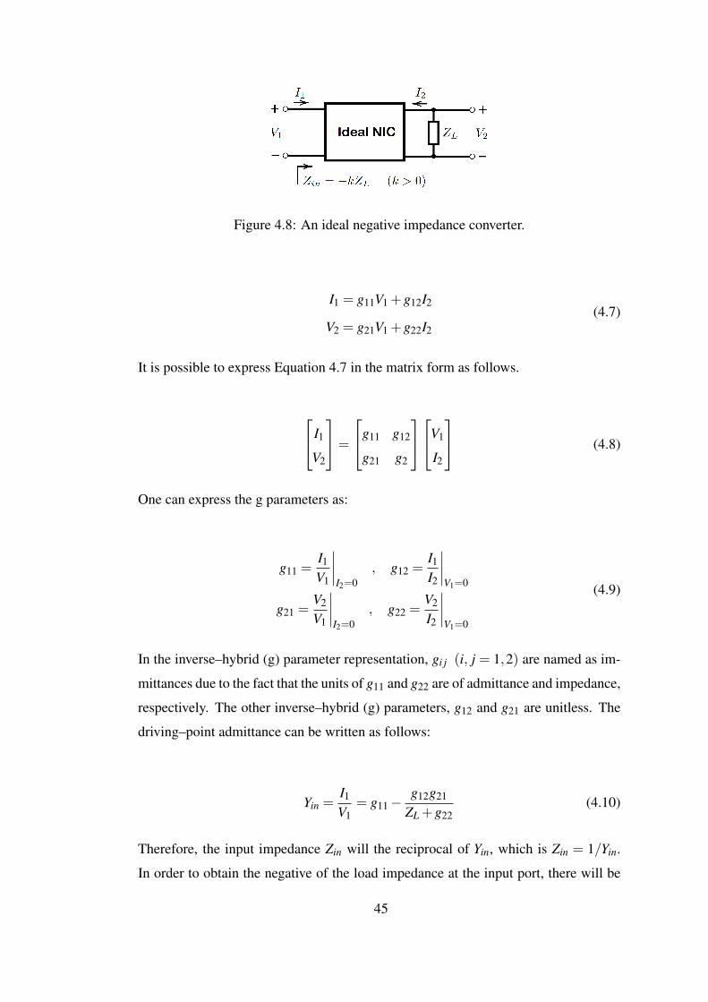
Figure 4.8: An ideal negative impedance converter.
I1 = g11V1 +g12I2
V2 = g21V1 +g22I2
(4.7)
It is possible to express Equation 4.7 in the matrix form as follows.
I1
V2
=
g11 g12
g21 g2
V1
I2
(4.8)
One can express the g parameters as:
g11 =I1
V1
∣∣∣∣I2=0
, g12 =I1
I2
∣∣∣∣V1=0
g21 =V2
V1
∣∣∣∣I2=0
, g22 =V2
I2
∣∣∣∣V1=0
(4.9)
In the inverse–hybrid (g) parameter representation, gi j (i, j = 1,2) are named as im-
mittances due to the fact that the units of g11 and g22 are of admittance and impedance,
respectively. The other inverse–hybrid (g) parameters, g12 and g21 are unitless. The
driving–point admittance can be written as follows:
Yin =I1
V1= g11−
g12g21
ZL +g22(4.10)
Therefore, the input impedance Zin will the reciprocal of Yin, which is Zin = 1/Yin.
In order to obtain the negative of the load impedance at the input port, there will be
45

some conditions that must be satisfied. We can obtain Zin =−ZL only if the following
gi j parameters take values as such:
g11 = 0
g22 = 0
g12g21 = 1
(4.11)
Figure 4.9 shows the inverse–hybrid (g) equivalent circuit with the conventinal volt-
age and current directions for a general two–port which is terminated with a passive
load ZL. This equivalent circuit is obtained using Equation 4.7 and Equation 4.9.
Figure 4.9: The inverse–hybrid (g) parameter representation of a general two–portnetwork.
The necessary conditions of a two–port to be a NIC are given in Equation 4.11. One
can observe that Equation 4.11 has two solutions which lead us to have voltage–
inversion or current–inversion negative impedance converters. To be able to obtain
g12g21 = 1, we should have either g12 and g21 to be positive or negative.
For an ideal voltage–inversion NIC, we have g11 and g22 are zero, and g12 and g21 are
both −1. This type of NIC changes the direction of the current flowing upon the load
impedance whereas the polarity of the voltage on the load impedance remains the
same. Let the current flowing on the load impedance ZL be IL. Also, let the voltage
on the load impedance be VL. Therefore, for a voltage–inversion NIC, the voltage and
current relationships can be written as:
V1 =−V2 =−VL
I1 = I2 = IL
(4.12)
46

The voltage–inversion negative impedance converter (VINIC) can be shown as a two-
port network with its corresponding voltage and current directions in Figure 4.10.
Figure 4.10: The voltage–inversion negative impedance converter (VINIC).
Similarly, for a current–inversion NIC, the direction of the current flowing on the load
resistance is inverted while the voltages remain the same. In this case, we have g11
and g22 are zero, and g12 and g21 are both 1. Therefore, for a current-inversion NIC,
the voltage and current relationships can be written as:
V1 =V2 =VL
I1 =−I2 =−IL
(4.13)
The current–inversion negative impedance converter (CINIC) can be shown as a two-
port network with its corresponding voltage and current directions in Figure 4.11.
Figure 4.11: The current–inversion negative impedance converter (CINIC).
The g–parameter matrices of voltage–inversion and current–inversion NICs can be
expressed as:
47
g =
0 −1
−1 0
for voltage-inversion NICs
g =
0 1
1 0
for current-inversion NICs
(4.14)
The voltage–inversion and current–inversion NIC circuits are the ideal cases in which
the two specific solutions of Equation 4.11; however, one can get g12 and g21 values
different than 1 or −1 in order to obtain a NIC as long as their multiplication satisfies
g12g21 = 1.
As it is seen from the Equation 4.10, practical negative impedance converters devi-
ate from the ideal case due to the presence of parasitic immittances: g11 and g22.
Even if this nonideal effects are small, they will still affect the performance the NICs
adversely. A close examination of Equation 3.4 can reveal that g11 will lower the neg-
ative admittance obtained by the NIC circuit. To minimize or annihilate the effects of
parasitic immittances, shunt and/or series passive impedances may be attached in Port
1 and Port 2 of the nonideal NIC. In addition to the parasitic immittances, the gain
product g12g21 will have the predominant effect on the negative impedance converter
performance.
4.2.2 Negative–Gm Oscillators
Up to this point, the two–port characteristics of negative impedance converters have
been investigated. While analyzing NICs as two–port devices, the active devices uti-
lized inside the two–port network have not been considered. In the following sections,
transistor and opamp negative impedance converters are investigated. Before going
into the detailed investigation of transistor and opamp NIC circuits, first, the concept
of negative resistance and negative–Gm oscillators should be introduced. Transis-
tor negative impedance converters, as shown in Section 4.2.1, have a cross–coupled
structure which is generally used to realize cross–coupled oscillators. Having a posi-
tive feedback structure, the NIC characteristics tend to be instable at some frequencies
which must be examined due to the fact that it is not desired to have a growing oscil-
48
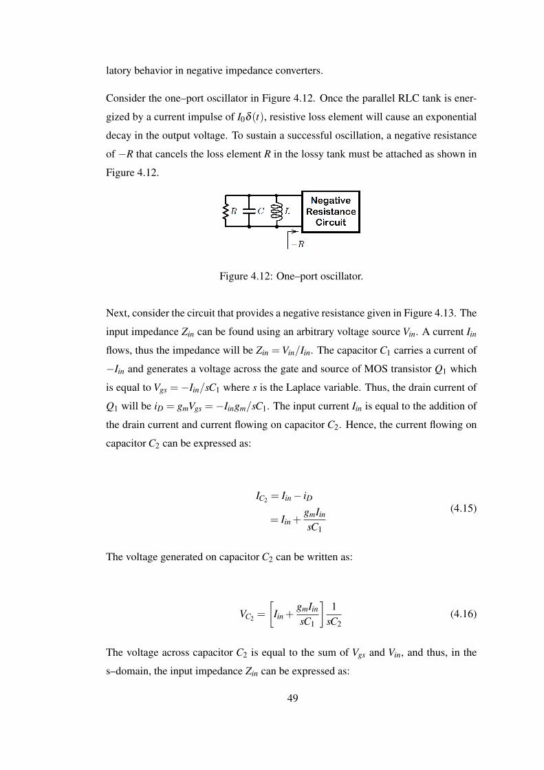
latory behavior in negative impedance converters.
Consider the one–port oscillator in Figure 4.12. Once the parallel RLC tank is ener-
gized by a current impulse of I0δ (t), resistive loss element will cause an exponential
decay in the output voltage. To sustain a successful oscillation, a negative resistance
of −R that cancels the loss element R in the lossy tank must be attached as shown in
Figure 4.12.
Figure 4.12: One–port oscillator.
Next, consider the circuit that provides a negative resistance given in Figure 4.13. The
input impedance Zin can be found using an arbitrary voltage source Vin. A current Iin
flows, thus the impedance will be Zin =Vin/Iin. The capacitor C1 carries a current of
−Iin and generates a voltage across the gate and source of MOS transistor Q1 which
is equal to Vgs =−Iin/sC1 where s is the Laplace variable. Thus, the drain current of
Q1 will be iD = gmVgs =−Iingm/sC1. The input current Iin is equal to the addition of
the drain current and current flowing on capacitor C2. Hence, the current flowing on
capacitor C2 can be expressed as:
IC2 = Iin− iD
= Iin +gmIin
sC1
(4.15)
The voltage generated on capacitor C2 can be written as:
VC2 =
[Iin +
gmIin
sC1
]1
sC2(4.16)
The voltage across capacitor C2 is equal to the sum of Vgs and Vin, and thus, in the
s–domain, the input impedance Zin can be expressed as:
49
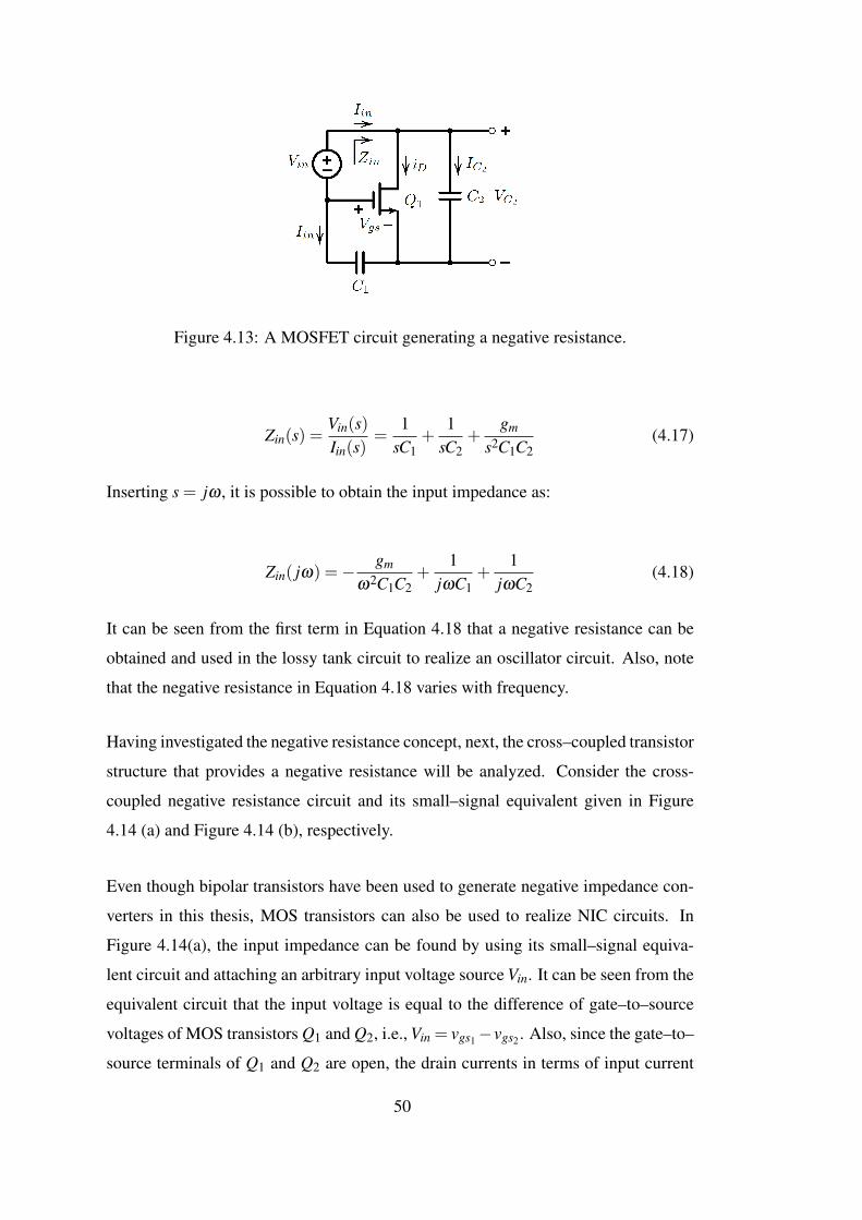
Figure 4.13: A MOSFET circuit generating a negative resistance.
Zin(s) =Vin(s)Iin(s)
=1
sC1+
1sC2
+gm
s2C1C2(4.17)
Inserting s = jω , it is possible to obtain the input impedance as:
Zin( jω) =− gm
ω2C1C2+
1jωC1
+1
jωC2(4.18)
It can be seen from the first term in Equation 4.18 that a negative resistance can be
obtained and used in the lossy tank circuit to realize an oscillator circuit. Also, note
that the negative resistance in Equation 4.18 varies with frequency.
Having investigated the negative resistance concept, next, the cross–coupled transistor
structure that provides a negative resistance will be analyzed. Consider the cross-
coupled negative resistance circuit and its small–signal equivalent given in Figure
4.14 (a) and Figure 4.14 (b), respectively.
Even though bipolar transistors have been used to generate negative impedance con-
verters in this thesis, MOS transistors can also be used to realize NIC circuits. In
Figure 4.14(a), the input impedance can be found by using its small–signal equiva-
lent circuit and attaching an arbitrary input voltage source Vin. It can be seen from the
equivalent circuit that the input voltage is equal to the difference of gate–to–source
voltages of MOS transistors Q1 and Q2, i.e., Vin = vgs1−vgs2 . Also, since the gate–to–
source terminals of Q1 and Q2 are open, the drain currents in terms of input current
50
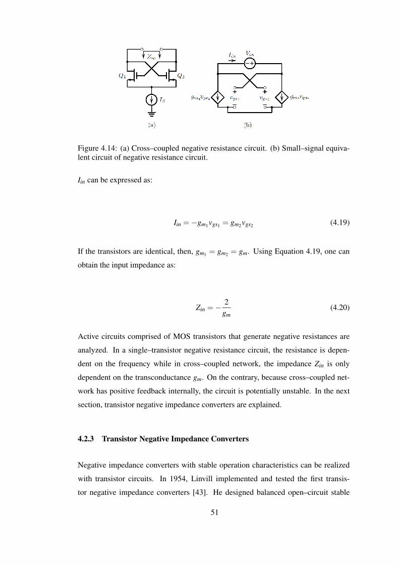
Figure 4.14: (a) Cross–coupled negative resistance circuit. (b) Small–signal equiva-lent circuit of negative resistance circuit.
Iin can be expressed as:
Iin =−gm1vgs1 = gm2vgs2 (4.19)
If the transistors are identical, then, gm1 = gm2 = gm. Using Equation 4.19, one can
obtain the input impedance as:
Zin =−2
gm(4.20)
Active circuits comprised of MOS transistors that generate negative resistances are
analyzed. In a single–transistor negative resistance circuit, the resistance is depen-
dent on the frequency while in cross–coupled network, the impedance Zin is only
dependent on the transconductance gm. On the contrary, because cross–coupled net-
work has positive feedback internally, the circuit is potentially unstable. In the next
section, transistor negative impedance converters are explained.
4.2.3 Transistor Negative Impedance Converters
Negative impedance converters with stable operation characteristics can be realized
with transistor circuits. In 1954, Linvill implemented and tested the first transis-
tor negative impedance converters [43]. He designed balanced open–circuit stable
51
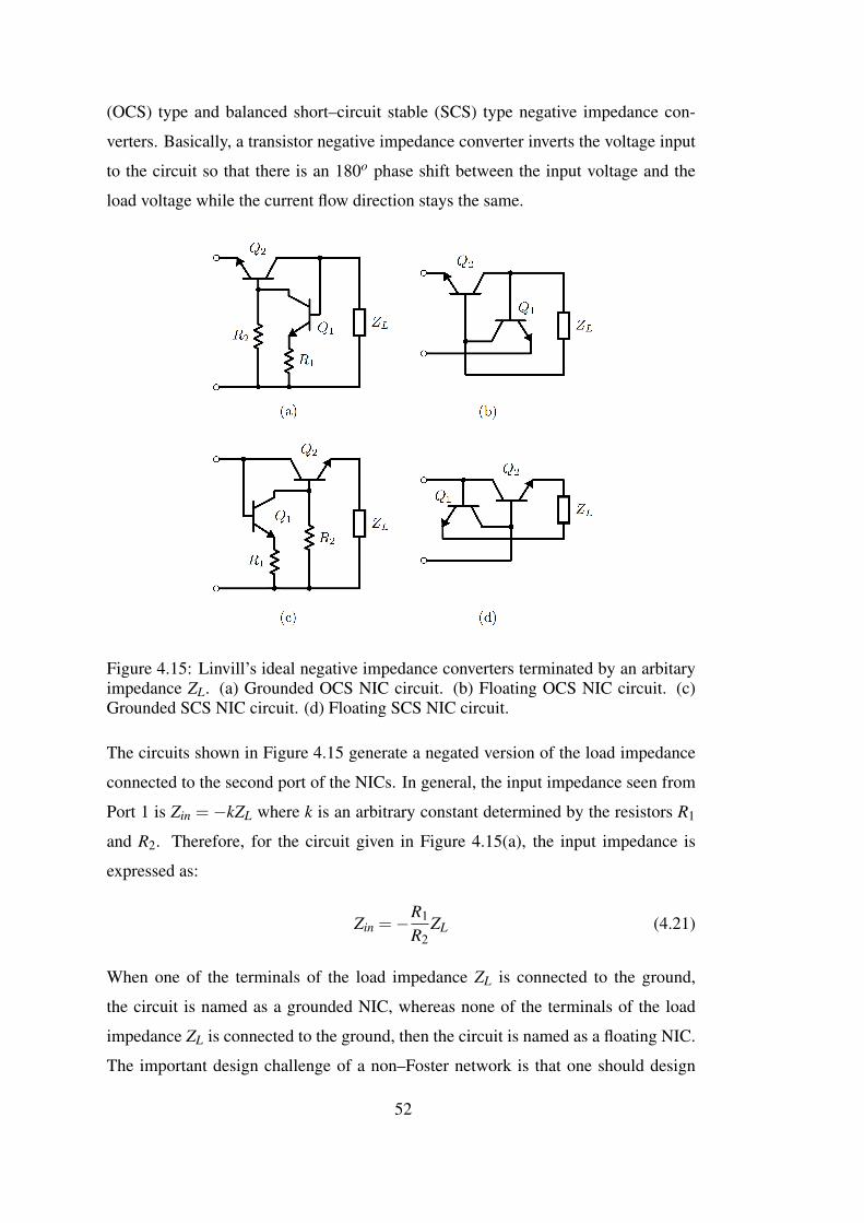
(OCS) type and balanced short–circuit stable (SCS) type negative impedance con-
verters. Basically, a transistor negative impedance converter inverts the voltage input
to the circuit so that there is an 180o phase shift between the input voltage and the
load voltage while the current flow direction stays the same.
Figure 4.15: Linvill’s ideal negative impedance converters terminated by an arbitaryimpedance ZL. (a) Grounded OCS NIC circuit. (b) Floating OCS NIC circuit. (c)Grounded SCS NIC circuit. (d) Floating SCS NIC circuit.
The circuits shown in Figure 4.15 generate a negated version of the load impedance
connected to the second port of the NICs. In general, the input impedance seen from
Port 1 is Zin = −kZL where k is an arbitrary constant determined by the resistors R1
and R2. Therefore, for the circuit given in Figure 4.15(a), the input impedance is
expressed as:
Zin =−R1
R2ZL (4.21)
When one of the terminals of the load impedance ZL is connected to the ground,
the circuit is named as a grounded NIC, whereas none of the terminals of the load
impedance ZL is connected to the ground, then the circuit is named as a floating NIC.
The important design challenge of a non–Foster network is that one should design
52

a NIC circuit that provides a negative impedance that can be used over the desired
frequency range for impedance cancellation without causing an unstable operation.
The concepts of short–circuit and open–circuit stability are related to the poles or
zeros of the impedance of a two–terminal linear network (one–port). Linvill stated
that the open–circuit stable NICs are the circuits whose input terminals are connected
to the emitters of the transistors [43]. Similarly, for short–circuit stable NICs, the
input terminals are connected to the collectors of the transistors.
The inherent characteristic of negative impedance converters has been asserted by
Brownlie [14] and Hoskins [15]. As indicated in [6], a practical two–port active
device functioning as a NIC must be OCS at one–port and SCS at the other port,
which is named as Brownlie–Hoskins theorem. It can be deduced from the theorem
that the load impedances to be connected to the ports of any NIC are constrained by
the inherent stability feature of negative impedance converters. Consider the circuit
given in Figure 4.16. Port 1 and Port 2 are terminated by Z1 and Z2, respectively. The
input impedance seen from Port 1 and Port 2 are Zin1 and Zin2, respectively.
Figure 4.16: Demonstration of Brownlie–Hoskins theorem. Port 1 and Port 2 areterminated by impedances Z1 and Z2, respectively.
The required conditions for OCS and SCS ports can be given as [6]:
|Z1| ≥ |Zin1| (4.22)
|Z2| ≤ |Zin2| (4.23)
In this thesis, Linvill’s floating OCS negative impedance converter shown in Figure
4.17 has been used to obtain a negative capacitor. It must be noted that a floating NIC
topology is selected due to the fact that it is desired to connect the designed non–
Foster element (negative capacitor) in series with the monopole antenna. Whether
53
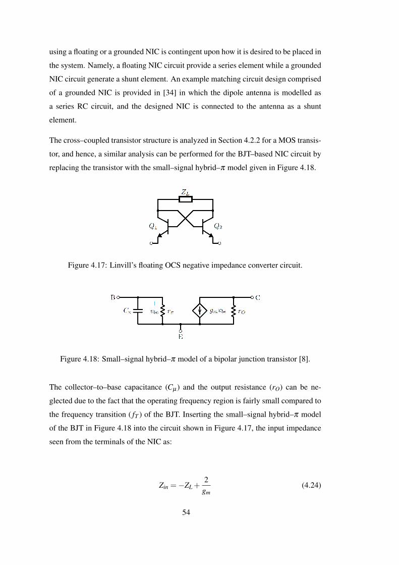
using a floating or a grounded NIC is contingent upon how it is desired to be placed in
the system. Namely, a floating NIC circuit provide a series element while a grounded
NIC circuit generate a shunt element. An example matching circuit design comprised
of a grounded NIC is provided in [34] in which the dipole antenna is modelled as
a series RC circuit, and the designed NIC is connected to the antenna as a shunt
element.
The cross–coupled transistor structure is analyzed in Section 4.2.2 for a MOS transis-
tor, and hence, a similar analysis can be performed for the BJT–based NIC circuit by
replacing the transistor with the small–signal hybrid–π model given in Figure 4.18.
Figure 4.17: Linvill’s floating OCS negative impedance converter circuit.
Figure 4.18: Small–signal hybrid–π model of a bipolar junction transistor [8].
The collector–to–base capacitance (Cµ ) and the output resistance (rO) can be ne-
glected due to the fact that the operating frequency region is fairly small compared to
the frequency transition ( fT ) of the BJT. Inserting the small–signal hybrid–π model
of the BJT in Figure 4.18 into the circuit shown in Figure 4.17, the input impedance
seen from the terminals of the NIC as:
Zin =−ZL +2
gm(4.24)
54
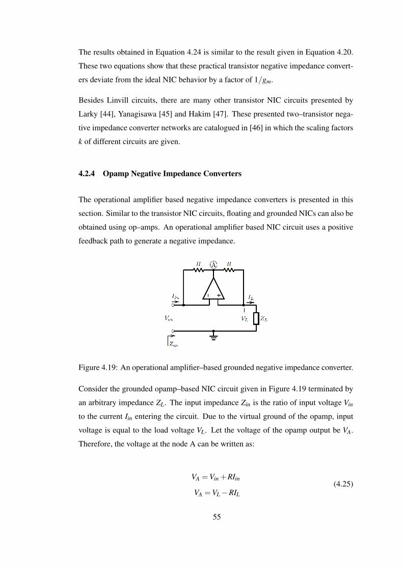
The results obtained in Equation 4.24 is similar to the result given in Equation 4.20.
These two equations show that these practical transistor negative impedance convert-
ers deviate from the ideal NIC behavior by a factor of 1/gm.
Besides Linvill circuits, there are many other transistor NIC circuits presented by
Larky [44], Yanagisawa [45] and Hakim [47]. These presented two–transistor nega-
tive impedance converter networks are catalogued in [46] in which the scaling factors
k of different circuits are given.
4.2.4 Opamp Negative Impedance Converters
The operational amplifier based negative impedance converters is presented in this
section. Similar to the transistor NIC circuits, floating and grounded NICs can also be
obtained using op–amps. An operational amplifier based NIC circuit uses a positive
feedback path to generate a negative impedance.
Figure 4.19: An operational amplifier–based grounded negative impedance converter.
Consider the grounded opamp–based NIC circuit given in Figure 4.19 terminated by
an arbitrary impedance ZL. The input impedance Zin is the ratio of input voltage Vin
to the current Iin entering the circuit. Due to the virtual ground of the opamp, input
voltage is equal to the load voltage VL. Let the voltage of the opamp output be VA.
Therefore, the voltage at the node A can be written as:
VA =Vin +RIin
VA =VL−RIL
(4.25)
55

Equating the node voltage expressions in Equation 4.25, one can obtain:
Iin =−IL (4.26)
As it is seen from Equation 4.26, this opamp NIC circuit is of current–inversion type.
Using Equation 4.26, the input impedance can be written as:
Zin =Vin
Iin=−VL
IL=−ZL (4.27)
Figure 4.20 shows an opamp–based floating NIC in which an arbitary impedance ZL
is connected to Port 2. The same impedance is also connected as the load of the NIC
to cancel the impedance at Port 2. Using the virtual ground property of the opamp,
the voltage on the load connected in between the opamps can be written as:
VL =Vin−V2 (4.28)
Therefore, the current flowing on the load can be written as:
IL =Vin−V2
ZL(4.29)
Figure 4.20: An operational amplifier–based floating negative impedance converter.
56
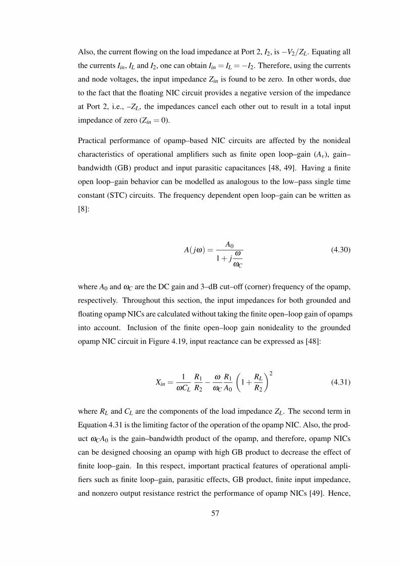
Also, the current flowing on the load impedance at Port 2, I2, is−V2/ZL. Equating all
the currents Iin, IL and I2, one can obtain Iin = IL =−I2. Therefore, using the currents
and node voltages, the input impedance Zin is found to be zero. In other words, due
to the fact that the floating NIC circuit provides a negative version of the impedance
at Port 2, i.e., –ZL, the impedances cancel each other out to result in a total input
impedance of zero (Zin = 0).
Practical performance of opamp–based NIC circuits are affected by the nonideal
characteristics of operational amplifiers such as finite open loop–gain (Av), gain–
bandwidth (GB) product and input parasitic capacitances [48, 49]. Having a finite
open loop–gain behavior can be modelled as analogous to the low–pass single time
constant (STC) circuits. The frequency dependent open loop–gain can be written as
[8]:
A( jω) =A0
1+ jω
ωC
(4.30)
where A0 and ωC are the DC gain and 3–dB cut–off (corner) frequency of the opamp,
respectively. Throughout this section, the input impedances for both grounded and
floating opamp NICs are calculated without taking the finite open–loop gain of opamps
into account. Inclusion of the finite open–loop gain nonideality to the grounded
opamp NIC circuit in Figure 4.19, input reactance can be expressed as [48]:
Xin =1
ωCL
R1
R2− ω
ωC
R1
A0
(1+
RL
R2
)2
(4.31)
where RL and CL are the components of the load impedance ZL. The second term in
Equation 4.31 is the limiting factor of the operation of the opamp NIC. Also, the prod-
uct ωCA0 is the gain–bandwidth product of the opamp, and therefore, opamp NICs
can be designed choosing an opamp with high GB product to decrease the effect of
finite loop–gain. In this respect, important practical features of operational ampli-
fiers such as finite loop–gain, parasitic effects, GB product, finite input impedance,
and nonzero output resistance restrict the performance of opamp NICs [49]. Hence,
57
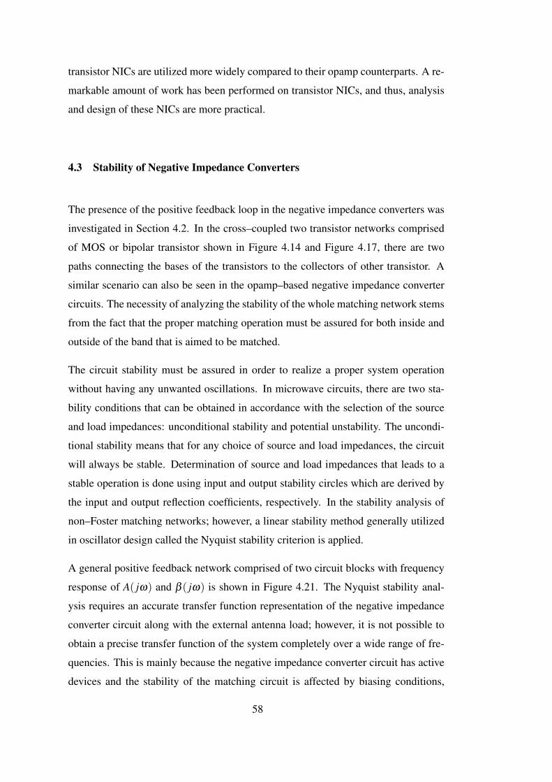
transistor NICs are utilized more widely compared to their opamp counterparts. A re-
markable amount of work has been performed on transistor NICs, and thus, analysis
and design of these NICs are more practical.
4.3 Stability of Negative Impedance Converters
The presence of the positive feedback loop in the negative impedance converters was
investigated in Section 4.2. In the cross–coupled two transistor networks comprised
of MOS or bipolar transistor shown in Figure 4.14 and Figure 4.17, there are two
paths connecting the bases of the transistors to the collectors of other transistor. A
similar scenario can also be seen in the opamp–based negative impedance converter
circuits. The necessity of analyzing the stability of the whole matching network stems
from the fact that the proper matching operation must be assured for both inside and
outside of the band that is aimed to be matched.
The circuit stability must be assured in order to realize a proper system operation
without having any unwanted oscillations. In microwave circuits, there are two sta-
bility conditions that can be obtained in accordance with the selection of the source
and load impedances: unconditional stability and potential unstability. The uncondi-
tional stability means that for any choice of source and load impedances, the circuit
will always be stable. Determination of source and load impedances that leads to a
stable operation is done using input and output stability circles which are derived by
the input and output reflection coefficients, respectively. In the stability analysis of
non–Foster matching networks; however, a linear stability method generally utilized
in oscillator design called the Nyquist stability criterion is applied.
A general positive feedback network comprised of two circuit blocks with frequency
response of A( jω) and β ( jω) is shown in Figure 4.21. The Nyquist stability anal-
ysis requires an accurate transfer function representation of the negative impedance
converter circuit along with the external antenna load; however, it is not possible to
obtain a precise transfer function of the system completely over a wide range of fre-
quencies. This is mainly because the negative impedance converter circuit has active
devices and the stability of the matching circuit is affected by biasing conditions,
58

transmission–line effects (PCB layout variables), the passive load connected to the
NIC and the external load (the antenna).
Figure 4.21: A general positive feedback circuit.
Using the feedback network given in Figure 4.21, the closed–loop transfer function
of the positive feedback circuit can be written as:
A f ( jω) =Y ( jω)
X( jω)=
A( jω)
1−A( jω)β ( jω)(4.32)
where the A f ( jω) is the closed–loop transfer function. The product A( jω)β ( jω) is
the loop–gain whose value must be unity in order to have oscillations. This is the
very well–known Barkhausen criterion [50]. The denominator in Equation 4.32 is
named as the characteristic equation, and thus, the stability of the closed–loop sys-
tem is determined by the zeros of the characteristic equation. In order to analyze the
stability of the system, one should check whether the characteristic equation has any
right–half plane zeros or not using the Nyquist stability test. The loop–gain prod-
uct A( jω)β ( jω) is plotted in a polar graph named as Nyquist plot as the frequency
changes from −∞ to ∞. The closed–loop system is said to be unstable if the Nyquist
plot encircles the point (1, 0) with the clockwise direction.
Due to the fact that there are many factors that affect the stability of the complete
matching network as described above, AWR Microwave Office®, a modern commer-
cial simulation tool, will be utilized while analyzing the stability issues and the design
of the matching network.
59
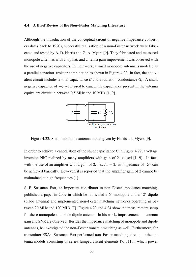
4.4 A Brief Review of the Non–Foster Matching Literature
Although the introduction of the conceptual circuit of negative impedance convert-
ers dates back to 1920s, successful realization of a non–Foster network were fabri-
cated and tested by A. D. Harris and G. A. Myers [9]. They fabricated and measured
monopole antennas with a top hat, and antenna gain improvement was observed with
the use of negative capacitors. In their work, a small monopole antenna is modeled as
a parallel capacitor–resistor combination as shown in Figure 4.22. In fact, the equiv-
alent circuit includes a total capacitance C and a radiation conductance Gr. A shunt
negative capacitor of −C were used to cancel the capacitance present in the antenna
equivalent circuit in between 0.5 MHz and 10 MHz [1, 9].
Figure 4.22: Small monopole antenna model given by Harris and Myers [9].
In order to achieve a cancellation of the shunt capacitance C in Figure 4.22, a voltage
inversion NIC realized by many amplifiers with gain of 2 is used [1, 9]. In fact,
with the use of an amplifier with a gain of 2, i.e., Av = 2, an impedance of –ZL can
be achieved basically. However, it is reported that the amplifier gain of 2 cannot be
maintained at high frequencies [1].
S. E. Sussman–Fort, an important contributor to non–Foster impedance matching,
published a paper in 2009 in which he fabricated a 6" monopole and a 12" dipole
(blade antenna) and implemented non–Foster matching networks operating in be-
tween 20 MHz and 120 MHz [7]. Figure 4.23 and 4.24 show the measurement setup
for these monopole and blade dipole antenna. In his work, improvements in antenna
gain and SNR are observed. Besides the impedance matching of monopole and dipole
antennas, he investigated the non–Foster transmit matching as well. Furthermore, for
transmitter ESAs, Sussman–Fort performed non–Foster matching circuits to the an-
tenna models consisting of series lumped circuit elements [7, 51] in which power
60
efficiency and biasing networks should be investigated in transmit applications. It
was stated that even for delivering moderate power levels to the antenna for radiation,
high terminal voltages will be needed due to voltage division [7]. To overcome this
high–voltage problem, a negative–LC matching was proposed. It was aimed that the
negative–LC combination will cause resonance in order to keep the voltages across
the NIC at a proper level for the deliverance of maximum power [1, 51]. In his
papers, he pointed out class–B and class–C types of biasing for power efficiency im-
provement; however, the circuit linearity was not examined. Additionally, although
it was stated that Middlebrook’s method [52] was employed for stability analysis, in
Sussman–Fort’s work, there were no explanation of how a stabilization network (or
element) was inserted into the non–Foster circuit. The grounded NIC (GNIC) circuit
used in [7] is presented in Appendix B. The results of the GNIC circuit have been
analyzed using AWR Microwave Office®, and demonstrated in the appendix as well.
Figure 4.23: The measurement setup presented in Sussman–Fort’s paper [7]. (a) 6"monopole antenna connected to 50Ω line. (b) 6" monopole antenna connected to afloating NIC.
In a recent work, non–Foster circuits based on BJT, graphene field effect transis-
tor (GFET) and resonant tunneling diode (RTD) were designed by D. S. Nagarkoti
[53, 54, 55]. In BJT–based non–Foster circuit, an OCS–type floating NIC topology
was used to generate a negative capacitor of –4.7 pF for matching a planar monopole.
It was presented that the biasing voltage was tuned to generate an optimal result. Be-
sides the BJT–based design, he also obtained negative capacitances and inductances
using GFET and RTD. Later, these aforementioned designs were applied to ESAs for
impedance matching over a wide band of frequencies. Additionally, noise analysis
was performed to find out how much the non–Foster circuit includes noise into the
system. The measured noise figure of the BJT–based non–Foster circuit was 9 to 14
61
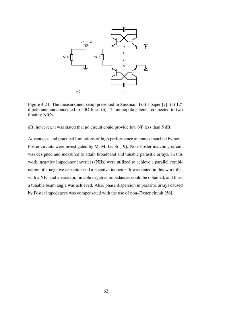
Figure 4.24: The measurement setup presented in Sussman–Fort’s paper [7]. (a) 12"dipole antenna connected to 50Ω line. (b) 12" monopole antenna connected to twofloating NICs.
dB; however, it was stated that no circuit could provide low NF less than 5 dB.
Advantages and practical limitations of high performance antennas matched by non–
Foster circuits were investigated by M. M. Jacob [19]. Non–Foster matching circuit
was designed and measured to attain broadband and tunable parasitic arrays. In this
work, negative impedance inverters (NIIs) were utilized to achieve a parallel combi-
nation of a negative capacitor and a negative inductor. It was stated in this work that
with a NIC and a varactor, tunable negative impedances could be obtained, and thus,
a tunable beam angle was achieved. Also, phase dispersion in parasitic arrays caused
by Foster impedances was compensated with the use of non–Foster circuit [56].
62
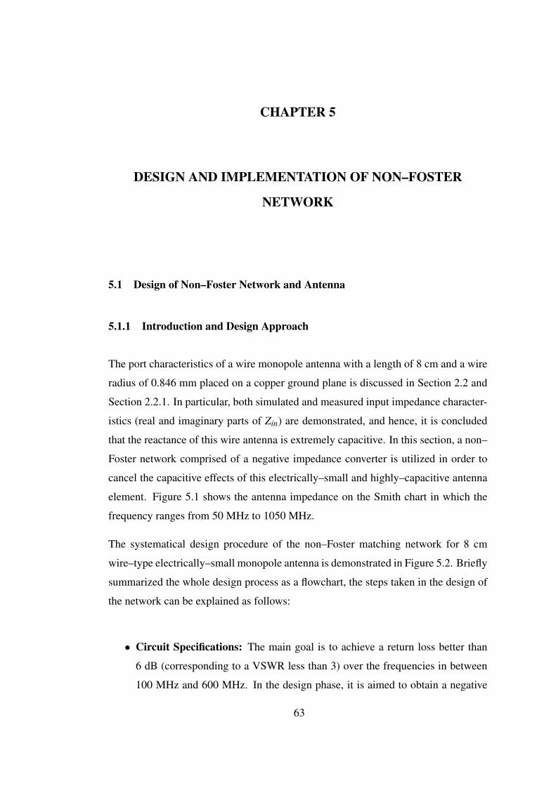
CHAPTER 5
DESIGN AND IMPLEMENTATION OF NON–FOSTER
NETWORK
5.1 Design of Non–Foster Network and Antenna
5.1.1 Introduction and Design Approach
The port characteristics of a wire monopole antenna with a length of 8 cm and a wire
radius of 0.846 mm placed on a copper ground plane is discussed in Section 2.2 and
Section 2.2.1. In particular, both simulated and measured input impedance character-
istics (real and imaginary parts of Zin) are demonstrated, and hence, it is concluded
that the reactance of this wire antenna is extremely capacitive. In this section, a non–
Foster network comprised of a negative impedance converter is utilized in order to
cancel the capacitive effects of this electrically–small and highly–capacitive antenna
element. Figure 5.1 shows the antenna impedance on the Smith chart in which the
frequency ranges from 50 MHz to 1050 MHz.
The systematical design procedure of the non–Foster matching network for 8 cm
wire–type electrically–small monopole antenna is demonstrated in Figure 5.2. Briefly
summarized the whole design process as a flowchart, the steps taken in the design of
the network can be explained as follows:
• Circuit Specifications: The main goal is to achieve a return loss better than
6 dB (corresponding to a VSWR less than 3) over the frequencies in between
100 MHz and 600 MHz. In the design phase, it is aimed to obtain a negative
63

Figure 5.1: Measured return loss for the monopole wire antenna depicted in Figure2.4. S–parameter data for the monopole antenna is taken in between 50 MHz–1050MHz range with 1 MHz increments. The return loss line on the Smith chart traces theplot in the clockwise direction.
capacitor that cancels the highly–reactive part of the input impedance over a
wide range of frequencies. In the designed NIC circuit, parameters that affect
the return loss and input impedance have been optimized for better results.
• Selection of the NIC Circuit Topology: Once the design goals are set, the
next step is to select the NIC circuit topology. As discussed in Section 4.2.3,
Linvill’s transistor negative impedance converters offer stable negative impedance
characteristics [43]. Among the four combinations of Linvill’s NICs, in this
thesis, Linvill’s floating OCS NIC is selected as the circuit topology owing to
the following reason: utilization of a floating element is very convenient due
to the fact that the whole NIC circuit can be implemented as a two–terminal
circuit element which can also be placed in between the antenna terminals and
the other RF sections.
• Non–Foster Circuit Design: Once the circuit topology is determined, first, RF
transistors must be selected and afterwards, the bias circuit must be designed.
The transistor selection and bias circuit design are explained in more detail
later. Upon the completion of the bias circuit design, the antenna impedance
measurement must be carried out so that the monopole antenna equivalent cir-
cuit can be obtained. The load of the negative impedance converter, CL, is
64

determined in accordance with the antenna equivalent circuit.
• Stability Analysis: As discussed in Section 4.3, NIC circuits are potentially
unstable owing to the positive feedback loop. In this respect, inevitability of
stability analysis of the whole matching network is apparent for the circuit de-
signer in order to achieve a stable operation. Stability of the designed non–
Foster matching network is analyzed using AWR Microwave Office®.
• Fabrication and Measurement: Once stability analysis is completed and the
circuit can provide a good matching characteristics, layout must be drawn, PCB
is fabricated and the monopole antenna with matching circuit is measured.
The matching network comprised of a negative capacitor is designed using two BFU550
transistors acquired by NXP Semiconductors. BFU5XX family of transistors are cho-
sen due to the fact that they can support small–signal to medium power applications
up to 2 GHz. Also, transistor BFU550 has a low noise figure (NFmin = 0.7 dB at
900 MHz) and its frequency transition ( fT ) is 11 GHz [57]. Having been pertinent to
the bandwidth of the transistor, transition frequency is the frequency point in which
the gain is unity [8]. The transition frequency for bipolar transistors is related to the
transconductance (gm), Cπ , Cµ , and the collector current IC. While designing the bias
circuit, it is substantial to bias the transistor at a collector current that gives rise to a
maximum frequency transition fT .
In the biasing circuit, a class–A type voltage–divider configuration with emitter tem-
perature stabilization is utilized. Additionally, a bias–tee circuit which is shown in
Figure 5.3 is added to the circuit to supply a DC current from the voltage source at
the collector of the transistor.
Upon the completion of the bias circuit design and non–Foster circuit, the stability
analysis is performed using AWR Microwave Office®. In order to examine the po-
tential unstable points of the non–Foster matching network, OSCTEST component
of AWR MWO® simulation tool is used. OSCTEST is an element inside the soft-
ware that is generally used for the design of oscillators. The open–loop analysis is
carried out by breaking the feedback loop and placing the component properly in the
circuit. Figure 5.4 demonstrates the OSCTEST component and how it is placed on
65
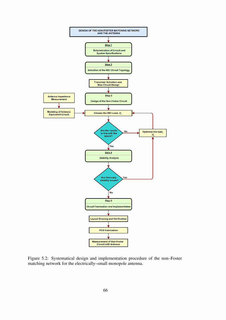
Figure 5.2: Systematical design and implementation procedure of the non–Fostermatching network for the electrically–small monopole antenna.
66
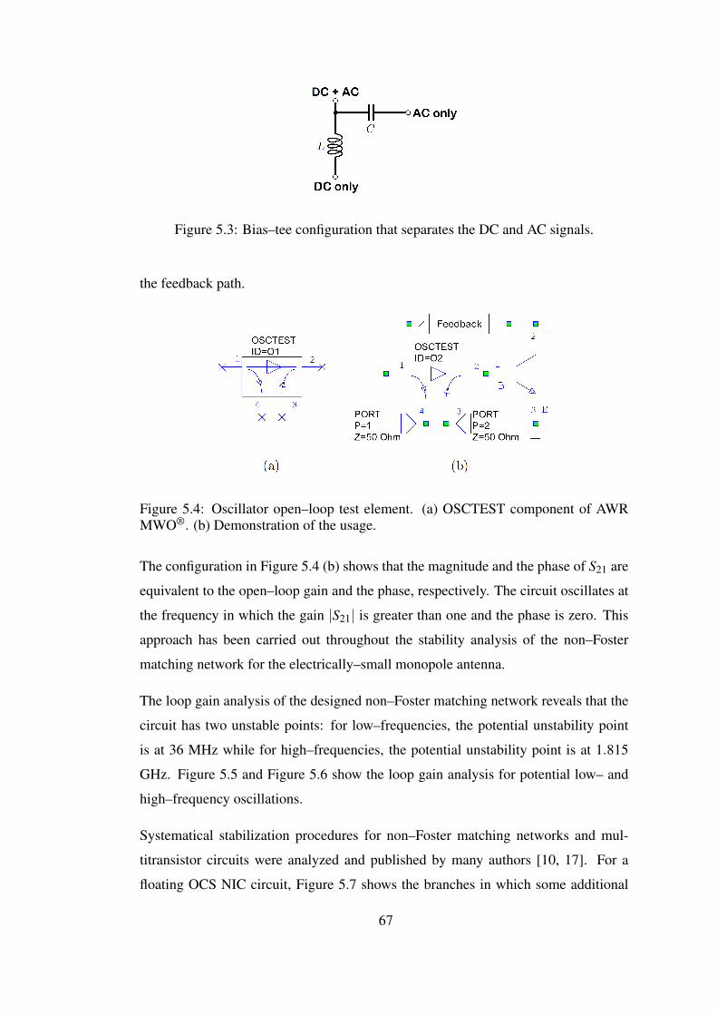
Figure 5.3: Bias–tee configuration that separates the DC and AC signals.
the feedback path.
Figure 5.4: Oscillator open–loop test element. (a) OSCTEST component of AWRMWO®. (b) Demonstration of the usage.
The configuration in Figure 5.4 (b) shows that the magnitude and the phase of S21 are
equivalent to the open–loop gain and the phase, respectively. The circuit oscillates at
the frequency in which the gain |S21| is greater than one and the phase is zero. This
approach has been carried out throughout the stability analysis of the non–Foster
matching network for the electrically–small monopole antenna.
The loop gain analysis of the designed non–Foster matching network reveals that the
circuit has two unstable points: for low–frequencies, the potential unstability point
is at 36 MHz while for high–frequencies, the potential unstability point is at 1.815
GHz. Figure 5.5 and Figure 5.6 show the loop gain analysis for potential low– and
high–frequency oscillations.
Systematical stabilization procedures for non–Foster matching networks and mul-
titransistor circuits were analyzed and published by many authors [10, 17]. For a
floating OCS NIC circuit, Figure 5.7 shows the branches in which some additional
67
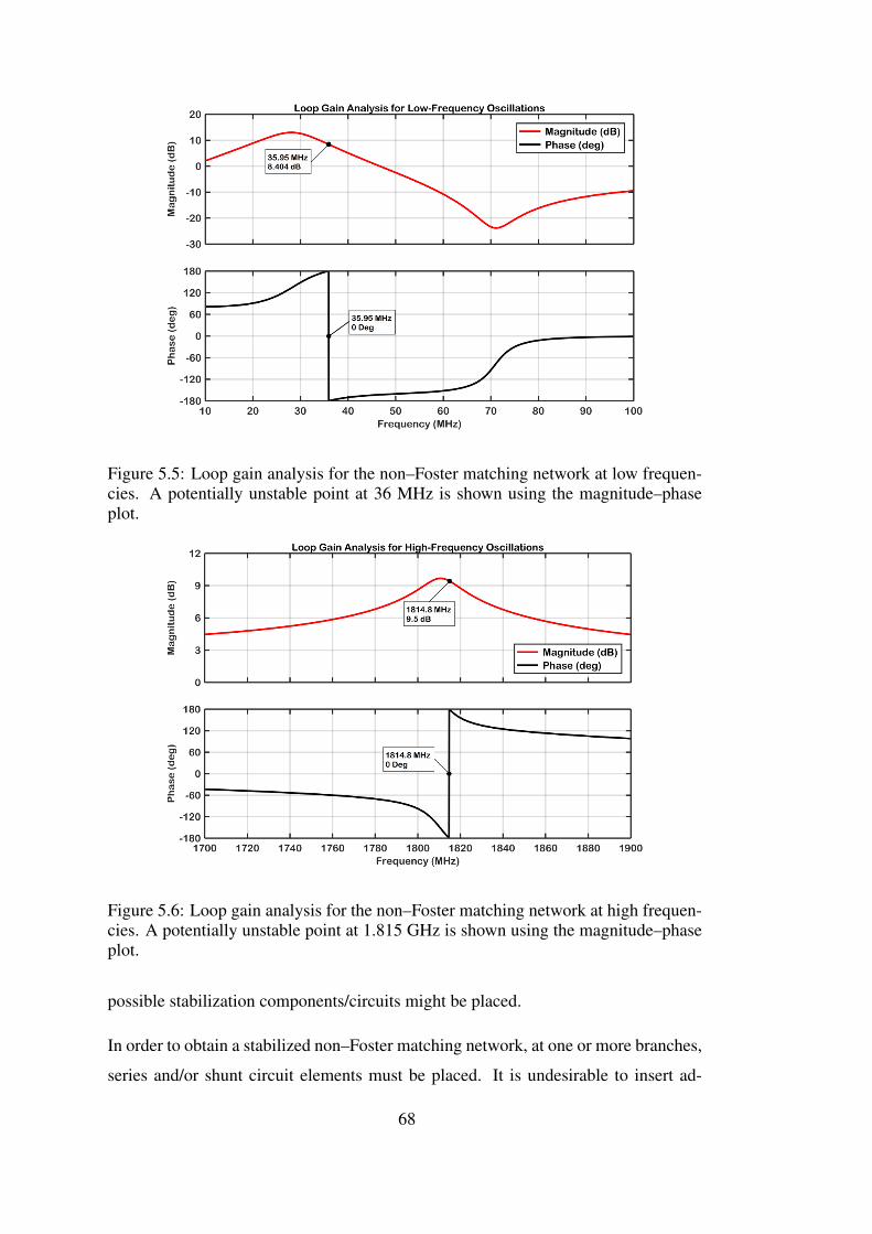
Figure 5.5: Loop gain analysis for the non–Foster matching network at low frequen-cies. A potentially unstable point at 36 MHz is shown using the magnitude–phaseplot.
Figure 5.6: Loop gain analysis for the non–Foster matching network at high frequen-cies. A potentially unstable point at 1.815 GHz is shown using the magnitude–phaseplot.
possible stabilization components/circuits might be placed.
In order to obtain a stabilized non–Foster matching network, at one or more branches,
series and/or shunt circuit elements must be placed. It is undesirable to insert ad-
68
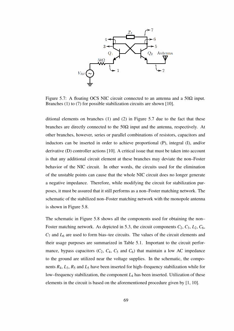
Figure 5.7: A floating OCS NIC circuit connected to an antenna and a 50Ω input.Branches (1) to (7) for possible stabilization circuits are shown [10].
ditional elements on branches (1) and (2) in Figure 5.7 due to the fact that these
branches are directly connected to the 50Ω input and the antenna, respectively. At
other branches, however, series or parallel combinations of resistors, capacitors and
inductors can be inserted in order to achieve proportional (P), integral (I), and/or
derivative (D) controller actions [10]. A critical issue that must be taken into account
is that any additional circuit element at these branches may deviate the non–Foster
behavior of the NIC circuit. In other words, the circuits used for the elimination
of the unstable points can cause that the whole NIC circuit does no longer generate
a negative impedance. Therefore, while modifying the circuit for stabilization pur-
poses, it must be assured that it still performs as a non–Foster matching network. The
schematic of the stabilized non–Foster matching network with the monopole antenna
is shown in Figure 5.8.
The schematic in Figure 5.8 shows all the components used for obtaining the non–
Foster matching network. As depicted in 5.3, the circuit components C2, C3, L2, C6,
C7 and L6 are used to form bias–tee circuits. The values of the circuit elements and
their usage purposes are summarized in Table 5.1. Important to the circuit perfor-
mance, bypass capacitors (C2, C4, C5 and C6) that maintain a low AC impedance
to the ground are utilized near the voltage supplies. In the schematic, the compo-
nents R4, L3, R5 and L5 have been inserted for high–frequency stabilization while for
low–frequency stabilization, the component L4 has been inserted. Utilization of these
elements in the circuit is based on the aforementioned procedure given by [1, 10].
69
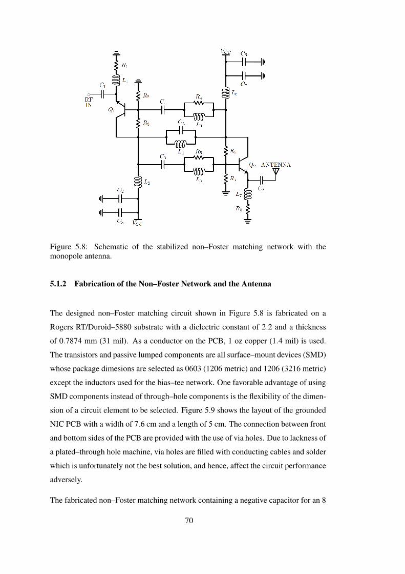
Figure 5.8: Schematic of the stabilized non–Foster matching network with themonopole antenna.
5.1.2 Fabrication of the Non–Foster Network and the Antenna
The designed non–Foster matching circuit shown in Figure 5.8 is fabricated on a
Rogers RT/Duroid–5880 substrate with a dielectric constant of 2.2 and a thickness
of 0.7874 mm (31 mil). As a conductor on the PCB, 1 oz copper (1.4 mil) is used.
The transistors and passive lumped components are all surface–mount devices (SMD)
whose package dimesions are selected as 0603 (1206 metric) and 1206 (3216 metric)
except the inductors used for the bias–tee network. One favorable advantage of using
SMD components instead of through–hole components is the flexibility of the dimen-
sion of a circuit element to be selected. Figure 5.9 shows the layout of the grounded
NIC PCB with a width of 7.6 cm and a length of 5 cm. The connection between front
and bottom sides of the PCB are provided with the use of via holes. Due to lackness of
a plated–through hole machine, via holes are filled with conducting cables and solder
which is unfortunately not the best solution, and hence, affect the circuit performance
adversely.
The fabricated non–Foster matching network containing a negative capacitor for an 8
70

Table 5.1: Numerical values and usage purposes of the circuit elements utilized in thenon–Foster matching network.
Component(s) Value Function
C1, C8 820 pF Coupling capacitors
C4, C5 10 nF Coupling capacitors
C2, C6 820 pF Bypass capacitors (bias–tee)
C3, C7 0.1 µF Bypass capacitors (bias–tee)
CL 2.4 pF Load of the NIC
R1, R8 200Ω Emitter–degeneration and biasing
R2, R7 10kΩ Biasing
R3, R6 10.4kΩ Biasing
L1, L7 2.2 µH Emitter–degeneration
L2, L6 2.2 µH RF choke (bias–tee)
L4 1.5 µH Low–frequency stabilization
L3, L5 18 nH High–frequency stabilization
R4, R5 100Ω High–frequency stabilization
cm–long wire–type monopole antenna placed on a copper ground plane is shown in
Figure 5.10.
Figure 5.9: Layout of the fabricated non–Foster matching circuit for the electrically–small antenna described in Section 2.2.
5.2 Simulated and Measured Results
In the design step of the non–Foster matching network and the antenna, circuit perfor-
mance and important parameters such as resistive and reactive parts of input impedance,
71
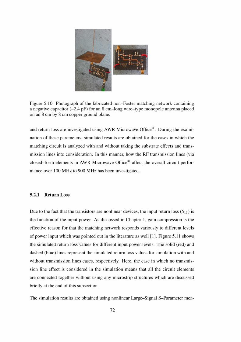
Figure 5.10: Photograph of the fabricated non–Foster matching network containinga negative capacitor (–2.4 pF) for an 8 cm–long wire–type monopole antenna placedon an 8 cm by 8 cm copper ground plane.
and return loss are investigated using AWR Microwave Office®. During the exami-
nation of these parameters, simulated results are obtained for the cases in which the
matching circuit is analyzed with and without taking the substrate effects and trans-
mission lines into consideration. In this manner, how the RF transmission lines (via
closed–form elements in AWR Microwave Office® affect the overall circuit perfor-
mance over 100 MHz to 900 MHz has been investigated.
5.2.1 Return Loss
Due to the fact that the transistors are nonlinear devices, the input return loss (S11) is
the function of the input power. As discussed in Chapter 1, gain compression is the
effective reason for that the matching network responds variously to different levels
of power input which was pointed out in the literature as well [1]. Figure 5.11 shows
the simulated return loss values for different input power levels. The solid (red) and
dashed (blue) lines represent the simulated return loss values for simulation with and
without transmission lines cases, respectively. Here, the case in which no transmis-
sion line effect is considered in the simulation means that all the circuit elements
are connected together without using any microstrip structures which are discussed
briefly at the end of this subsection.
The simulation results are obtained using nonlinear Large–Signal S–Parameter mea-
72
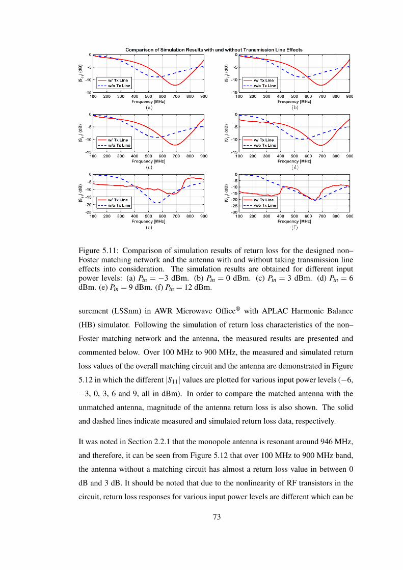
Figure 5.11: Comparison of simulation results of return loss for the designed non–Foster matching network and the antenna with and without taking transmission lineeffects into consideration. The simulation results are obtained for different inputpower levels: (a) Pin = −3 dBm. (b) Pin = 0 dBm. (c) Pin = 3 dBm. (d) Pin = 6dBm. (e) Pin = 9 dBm. (f) Pin = 12 dBm.
surement (LSSnm) in AWR Microwave Office® with APLAC Harmonic Balance
(HB) simulator. Following the simulation of return loss characteristics of the non–
Foster matching network and the antenna, the measured results are presented and
commented below. Over 100 MHz to 900 MHz, the measured and simulated return
loss values of the overall matching circuit and the antenna are demonstrated in Figure
5.12 in which the different |S11| values are plotted for various input power levels (−6,
−3, 0, 3, 6 and 9, all in dBm). In order to compare the matched antenna with the
unmatched antenna, magnitude of the antenna return loss is also shown. The solid
and dashed lines indicate measured and simulated return loss data, respectively.
It was noted in Section 2.2.1 that the monopole antenna is resonant around 946 MHz,
and therefore, it can be seen from Figure 5.12 that over 100 MHz to 900 MHz band,
the antenna without a matching circuit has almost a return loss value in between 0
dB and 3 dB. It should be noted that due to the nonlinearity of RF transistors in the
circuit, return loss responses for various input power levels are different which can be
73
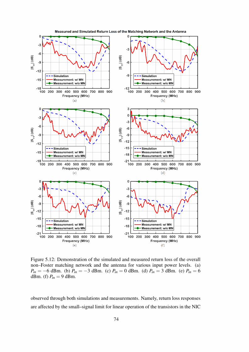
Figure 5.12: Demonstration of the simulated and measured return loss of the overallnon–Foster matching network and the antenna for various input power levels. (a)Pin = −6 dBm. (b) Pin = −3 dBm. (c) Pin = 0 dBm. (d) Pin = 3 dBm. (e) Pin = 6dBm. (f) Pin = 9 dBm.
observed through both simulations and measurements. Namely, return loss responses
are affected by the small–signal limit for linear operation of the transistors in the NIC
74

circuit when strong signals are applied at the input terminals of the matching circuit
[9]. As shown in Figure 5.12, an increase in the input power causes to attain a better
match. The discrepancy in between the simulated and measured results may stem
from the fact that the return loss simulations are performed using closed–form circuit
elements which are MLIN (microstrip line), MTEE (microstrip T–junction) and mi-
crostrip bends. These are the circuit blocks in AWR Microwave Office® that are used
to model microstrip structures and discontinuities and include the effects of dielectric
and conductive losses in the analysis. In addition, the DC power consumption of the
BJT transistors are calculated as 0.159 W. DC voltage sources supplies a total DC
power of 0.498 W, thus, transistors with low–power consumption can be connected
to the circuit in future designs instead of current transistors.
5.2.2 Input Impedance
For real and imaginary parts of the input impedance, effects of closed–form element
microstrip structures are analyzed as done for return loss in the previous section. The
results are demonstrated in Figure 5.13. As shown in the figure below, at lower fre-
quencies, different results can be obtained if microstrip structures of AWR Microwave
Office® are used.
The simulated and measured data for the real part of the input impedance of the
overall non–Foster matching network and the antenna over 100 MHz to 900 MHz are
demonstrated in Figure 5.14 in which the solid and dashed lines indicate measured
and simulated input impedance data (real part), respectively.
Knowing that one of the intrinsic properties of ESAs is that the real part of the input
impedance is very low compared to the imaginary part, Figure 5.14 shows an im-
provement on the resistive part for the monopole antenna. In that sense, non–Foster
matching circuits are not only useful for cancellation of the reactive part of the in-
put impedance but also can help on the improvement of the resistive part. Likewise,
simulated and measured data for the imaginary part of the input impedance of the
overall non–Foster matching network and the antenna over 100 MHz to 900 MHz are
demonstrated in Figure 5.15 in which the solid and dashed lines indicate measured
and simulated input impedance data (imaginary part), respectively.
75
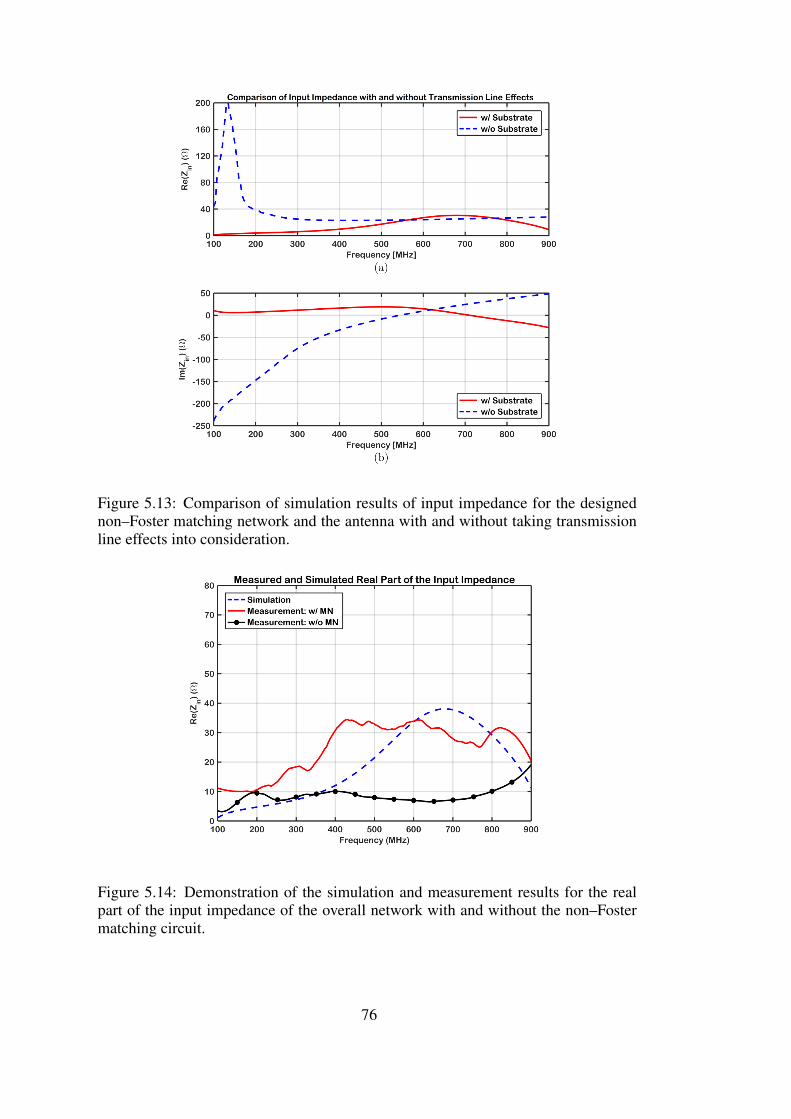
Figure 5.13: Comparison of simulation results of input impedance for the designednon–Foster matching network and the antenna with and without taking transmissionline effects into consideration.
Figure 5.14: Demonstration of the simulation and measurement results for the realpart of the input impedance of the overall network with and without the non–Fostermatching circuit.
76
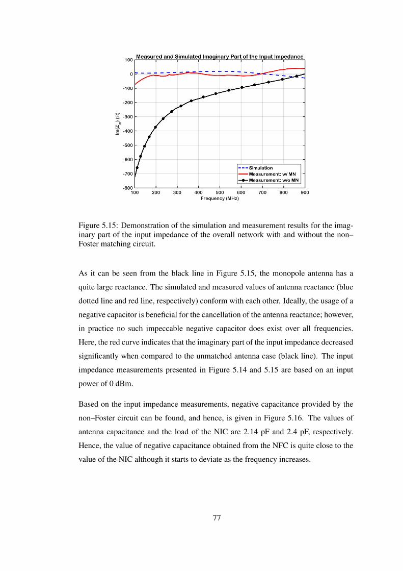
Figure 5.15: Demonstration of the simulation and measurement results for the imag-inary part of the input impedance of the overall network with and without the non–Foster matching circuit.
As it can be seen from the black line in Figure 5.15, the monopole antenna has a
quite large reactance. The simulated and measured values of antenna reactance (blue
dotted line and red line, respectively) conform with each other. Ideally, the usage of a
negative capacitor is beneficial for the cancellation of the antenna reactance; however,
in practice no such impeccable negative capacitor does exist over all frequencies.
Here, the red curve indicates that the imaginary part of the input impedance decreased
significantly when compared to the unmatched antenna case (black line). The input
impedance measurements presented in Figure 5.14 and 5.15 are based on an input
power of 0 dBm.
Based on the input impedance measurements, negative capacitance provided by the
non–Foster circuit can be found, and hence, is given in Figure 5.16. The values of
antenna capacitance and the load of the NIC are 2.14 pF and 2.4 pF, respectively.
Hence, the value of negative capacitance obtained from the NFC is quite close to the
value of the NIC although it starts to deviate as the frequency increases.
77

Figure 5.16: Negative capacitance obtained from the designed non–Foster circuit.
5.2.3 Antenna Gain
Non–Foster matching circuits are being utilized not only for the enhancement of port
characteristics and return loss but also the improvement of the antenna gain. In this
respect, the antenna gain measurements with and without non–Foster matching net-
work are performed in the frequencies between 150 MHz and 500 MHz. Figure 5.17
has been provided in order to demonstrate the gain measurement setup. Although the
figure is not drawn to scale, the reference antenna and the antenna under test (AUT)
are held as their ground planes are parallel to the ground floor.
Figure 5.17: Simple demonstration of the gain measurement setup. TX and AUTrefer to transmitter antenna and the antenna under test, respectively. The figure is notdrawn to scale.
The measurements have been recorded inside a closed room while a transmitter an-
78
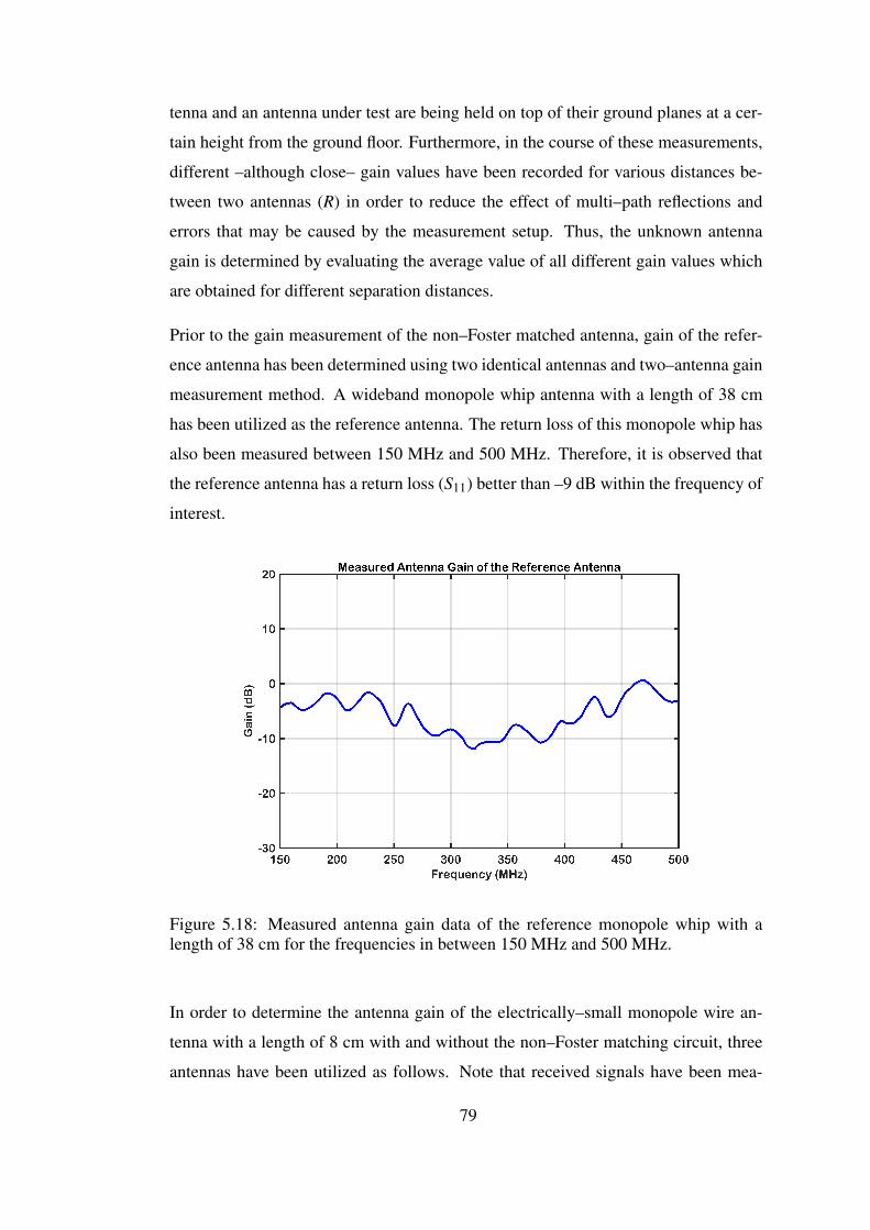
tenna and an antenna under test are being held on top of their ground planes at a cer-
tain height from the ground floor. Furthermore, in the course of these measurements,
different –although close– gain values have been recorded for various distances be-
tween two antennas (R) in order to reduce the effect of multi–path reflections and
errors that may be caused by the measurement setup. Thus, the unknown antenna
gain is determined by evaluating the average value of all different gain values which
are obtained for different separation distances.
Prior to the gain measurement of the non–Foster matched antenna, gain of the refer-
ence antenna has been determined using two identical antennas and two–antenna gain
measurement method. A wideband monopole whip antenna with a length of 38 cm
has been utilized as the reference antenna. The return loss of this monopole whip has
also been measured between 150 MHz and 500 MHz. Therefore, it is observed that
the reference antenna has a return loss (S11) better than –9 dB within the frequency of
interest.
Figure 5.18: Measured antenna gain data of the reference monopole whip with alength of 38 cm for the frequencies in between 150 MHz and 500 MHz.
In order to determine the antenna gain of the electrically–small monopole wire an-
tenna with a length of 8 cm with and without the non–Foster matching circuit, three
antennas have been utilized as follows. Note that received signals have been mea-
79
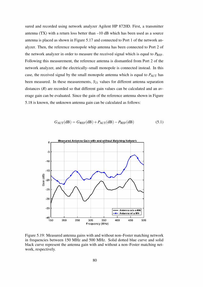
sured and recorded using network analyzer Agilent HP 8720D. First, a transmitter
antenna (TX) with a return loss better than –10 dB which has been used as a source
antenna is placed as shown in Figure 5.17 and connected to Port 1 of the network an-
alyzer. Then, the reference monopole whip antenna has been connected to Port 2 of
the network analyzer in order to measure the received signal which is equal to PREF.
Following this measurement, the reference antenna is dismantled from Port 2 of the
network analyzer, and the electrically–small monopole is connected instead. In this
case, the received signal by the small monopole antenna which is equal to PAUT has
been measured. In these measurements, S21 values for different antenna separation
distances (R) are recorded so that different gain values can be calculated and an av-
erage gain can be evaluated. Since the gain of the reference antenna shown in Figure
5.18 is known, the unknown antenna gain can be calculated as follows:
GAUT(dB) = GREF(dB)+PAUT(dB)−PREF(dB) (5.1)
Figure 5.19: Measured antenna gains with and without non–Foster matching networkin frequencies between 150 MHz and 500 MHz. Solid dotted blue curve and solidblack curve represent the antenna gain with and without a non–Foster matching net-work, respectively.
80
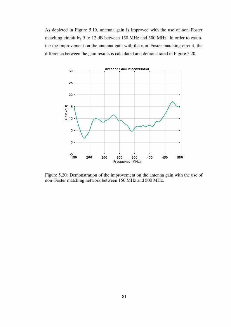
As depicted in Figure 5.19, antenna gain is improved with the use of non–Foster
matching circuit by 5 to 12 dB between 150 MHz and 500 MHz. In order to exam-
ine the improvement on the antenna gain with the non–Foster matching circuit, the
difference between the gain results is calculated and demonstrated in Figure 5.20.
Figure 5.20: Demonstration of the improvement on the antenna gain with the use ofnon–Foster matching network between 150 MHz and 500 MHz.
81

82
CHAPTER 6
CONCLUSION
6.1 Conclusion and Summary
Electrically–small wire monopole antennas generally possess high reactances and
very low resistances in their input impedances which leads these antennas to have
high quality factors (Q). This characteristic leads them to have a narrow operation
bandwidth. The basic objective of this thesis is to increase the performance of the
electrically–small antenna over a broad frequency range by means of non–Foster
matching networks (NFMs) comprised of negative impedance converters (NICs).
Brief information on the theory of electrically–small antennas is discussed in Chapter
2 where the monopole antenna used in this thesis is discussed. A wire antenna with
a length of 8 cm placed on a square copper ground plane (8 cm by 8 cm) has a huge
reactance compared to the radiation resistance in the frequency spectrum of interest.
Thus, non–Foster matching networks for such antennas can be utilized in order to
enhance port characteristics, return loss and antenna gain.
A reactively–loaded thin monopole antenna with a length of 20 cm placed on a square
ground plane (50 cm by 50 cm) has been designed using optimization algorithms.
The details of the design is presented in Chapter 3. Passive lumped elements can be
placed on the antenna at certain positions in order to modify the antenna current, and
thus, radiation characteristics of the antenna are enhanced. With the use of genetic
algorithms, the antenna load and the external matching network is designed. 6–dB
bandwidth of the reactively–loaded monopole antenna is measured to be 290 MHz,
and therefore, a broader matching is achieved with the use of reactive loading com-
83

pared to the unloaded monopole antenna.
In Chapter 4, the concept of non–Foster matching is discussed. In order to demon-
strate the Bode–Fano limit, an example of passive matching realized by lumped cir-
cuit elements is presented. The circuit is designed using optimization algorithms of
AWR Microwave Office®, and thus, the best result that this network provides is a
matching in between 355 MHz and 445 MHz. Being in line with Bode–Fano limit,
this passive circuit illustrates the need for an active matching network for broadband
operation. Furthermore, NIC circuits, stability issues and literature review of non–
Foster matching are discussed in Chapter 4 as well.
The design steps of non–Foster circuit for an ESA is investigated in Chapter 5. First,
the bias circuit of the non–Foster network is designed, and later on, the stability anal-
ysis is performed. Loop gain analysis predicts that the circuit is potentially unstable
at around 36 MHz and 1.815 GHz. According to the measurement data of 8 cm–long
wire antenna, the load of the NIC circuit is selected as 2.4 pF because the antenna
equivalent circuit is modelled as a series combination of a 2.14 pF capacitor and a
7.86 nH inductor. The designed non–Foster circuit is fabricated, implemented and
measured. Overall circuit performance is investigated between 100 MHz and 900
MHz. Upon fabricating the matching circuit for the antenna, it is shown that the
operation band of the electrically–small monopole antenna is improved mostly in be-
tween 200 MHz and 750 MHz. The input reflection coefficient (S11) as a function of
various input power levels are simulated, measured and presented. Better reflection
coefficients are obtained when higher input power levels are applied, and thus, for
transmitter antenna applications, this characteristic should be taken into account.
Furthermore, as shown in the figures of measured data for real and imaginary parts of
the input impedance, reactive part of the antenna is mostly cancelled, and the radiation
resistance is improved from a few ohms to 15–35 ohms. In addition, by means of a
reference antenna, antenna gains of the wire monopole with and without non–Foster
matching network are measured. Antenna gain of the reference monopole whip is also
measured and found to be in between 0 dB to –10 dB. It is shown that the matching
circuit improves the gain of the electrically–small wire monopole by 5 to 12 dB over
150 MHz and 500 MHz.
84

6.2 Future Work
In the light of the presented accomplishments in this thesis, the work done on non–
Foster matching of electrically–small antennas can further be improved and extended
with the future works as follows.
In this thesis, it is aimed to adjust the input impedance so that the imaginary part is
cancelled out and the real part is improved. Also, another important objective is to
enhance the return loss performance of the electrically–small monopole antenna with
the use of non–Foster matching network. As presented in Chapter 5, the matching
circuit is comprised of a resistive voltage–divider bias configuration which affect the
noise performance of the circuit adversely. Being key figure–of–merits for receivers,
signal–to–noise ratio (SNR) and noise figure (NF) should be considered for efficient
reception of the incoming signal. In this respect, implementation of current mirrors
for biasing the discrete transistors in the matching circuit could be a feasible solution
for noise performance. Furthermore, being comprised of active circuit elements such
as transistors, non–Foster circuits consume DC power. With the use of low–power
transistors, DC power consumption might be restrained [1]. Due to the nonlinear
nature of the transistors, for transmitter antennas, the power efficiency, 1–dB com-
pression point, IP3 and dynamic range (DR) should be investigated [19]. In order to
obtain high power efficiency in transmitter applications, various types of bias circuits
such as class–B or class–C biased NICs can be designed [51].
Instead of implementing the non–Foster matching networks and/or negative impedance
converters on printed circuit boards, integrated–circuit (IC) version of the non–Foster
matching circuits can be fabricated. The design and implementation of such inte-
grated non–Foster elements can be utilized for small compact antennas that can be
used in portable handheld units. Moreover, an integrated non–Foster element can
also reduce the DC power consumption. Published by Kolev in [58], a negative ca-
pacitor of –1 pF in between 1 GHz to 5 GHz is attained. The fabrication technology
is 0.25 µm pHEMT process [1, 58].
85

86
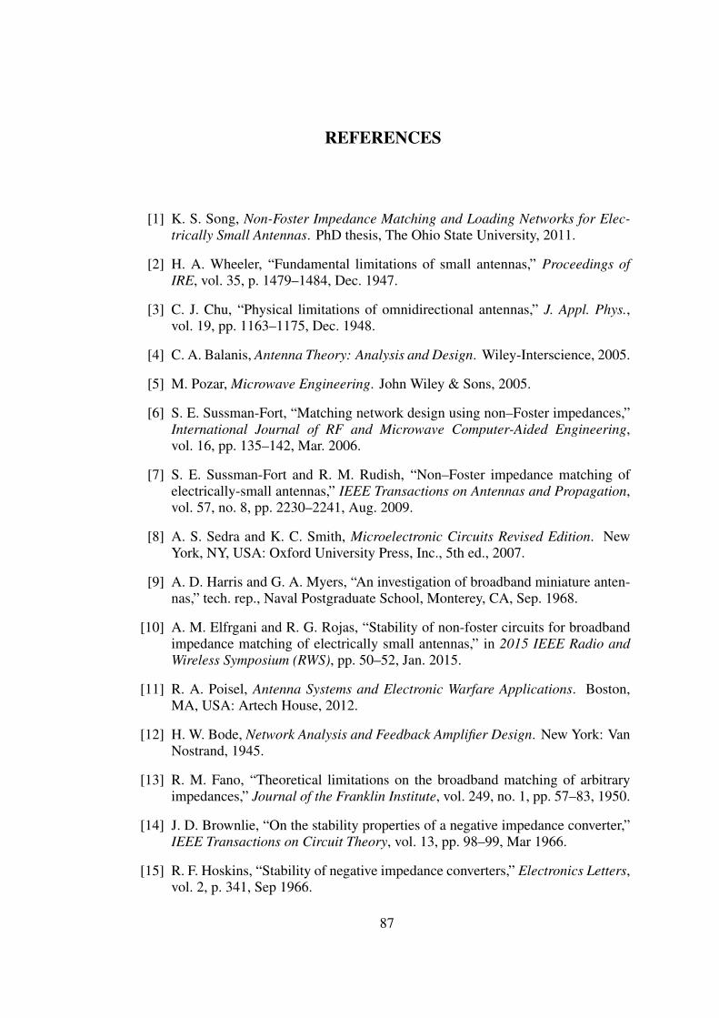
REFERENCES
[1] K. S. Song, Non-Foster Impedance Matching and Loading Networks for Elec-trically Small Antennas. PhD thesis, The Ohio State University, 2011.
[2] H. A. Wheeler, “Fundamental limitations of small antennas,” Proceedings ofIRE, vol. 35, p. 1479–1484, Dec. 1947.
[3] C. J. Chu, “Physical limitations of omnidirectional antennas,” J. Appl. Phys.,vol. 19, pp. 1163–1175, Dec. 1948.
[4] C. A. Balanis, Antenna Theory: Analysis and Design. Wiley-Interscience, 2005.
[5] M. Pozar, Microwave Engineering. John Wiley & Sons, 2005.
[6] S. E. Sussman-Fort, “Matching network design using non–Foster impedances,”International Journal of RF and Microwave Computer-Aided Engineering,vol. 16, pp. 135–142, Mar. 2006.
[7] S. E. Sussman-Fort and R. M. Rudish, “Non–Foster impedance matching ofelectrically-small antennas,” IEEE Transactions on Antennas and Propagation,vol. 57, no. 8, pp. 2230–2241, Aug. 2009.
[8] A. S. Sedra and K. C. Smith, Microelectronic Circuits Revised Edition. NewYork, NY, USA: Oxford University Press, Inc., 5th ed., 2007.
[9] A. D. Harris and G. A. Myers, “An investigation of broadband miniature anten-nas,” tech. rep., Naval Postgraduate School, Monterey, CA, Sep. 1968.
[10] A. M. Elfrgani and R. G. Rojas, “Stability of non-foster circuits for broadbandimpedance matching of electrically small antennas,” in 2015 IEEE Radio andWireless Symposium (RWS), pp. 50–52, Jan. 2015.
[11] R. A. Poisel, Antenna Systems and Electronic Warfare Applications. Boston,MA, USA: Artech House, 2012.
[12] H. W. Bode, Network Analysis and Feedback Amplifier Design. New York: VanNostrand, 1945.
[13] R. M. Fano, “Theoretical limitations on the broadband matching of arbitraryimpedances,” Journal of the Franklin Institute, vol. 249, no. 1, pp. 57–83, 1950.
[14] J. D. Brownlie, “On the stability properties of a negative impedance converter,”IEEE Transactions on Circuit Theory, vol. 13, pp. 98–99, Mar 1966.
[15] R. F. Hoskins, “Stability of negative impedance converters,” Electronics Letters,vol. 2, p. 341, Sep 1966.
87

[16] D. Segovia-Vargas, J. Jimenez-Martin, A. Parra-Cerrada, E. Ugarte-Munoz,L. Albarracin-Vargas, and V. Gonzalez-Posadas, “Stability analysis and designof negative impedance converters: application to circuit and small antennas,”Radioengineering, vol. 25, pp. 409–418, Sept. 2016.
[17] N. Ayllon, J. M. Collantes, A. Anakabe, I. Lizarraga, G. Soubercaze-Pun,and S. Forestier, “Systematic approach to the stabilization of multitransistorcircuits,” IEEE Transactions on Microwave Theory and Techniques, vol. 59,pp. 2073–2082, Aug 2011.
[18] B. Razavi, RF Microelectronics. Upper Saddle River, NJ, USA: Prentice HallPress, 2nd ed., 2011.
[19] M. M. Jacob, Non-Foster Circuits for High Performance Antennas: Advantagesand Practical Limitations. PhD thesis, University of California, San Diego,2016.
[20] J. D. Kraus, Antennas. New York: McGraw–Hill, 2nd ed., 1988.
[21] J. Long, M. M. Jacob, and D. F. Sievenpiper, “Broadband fast-wave propagationin a non-Foster circuit loaded waveguide,” IEEE Transactions on MicrowaveTheory and Techniques, vol. 62, pp. 789–798, April 2014.
[22] S. D. Rogers, C. M. Butler, and A. Q. Martin, “Design and realization of GA–optimized wire monopole and matching network with 20:1 bandwidth,” IEEETransactions on Antennas and Propagation, vol. 51, pp. 493–502, March.
[23] A. Boag, A. Boag, E. Michielssen, and R. Mittra, “Design of electrically loadedwire antennas using genetic algorithms,” IEEE Transactions on Antennas andPropagation, vol. 44, pp. 687–695, May 1996.
[24] Z. Altman, R. Mittra, and A. Boag, “New designs of ultra wide–band communi-cation antennas using a genetic algorithm,” IEEE Transactions on Antennas andPropagation, vol. 45, pp. 1494–1501, Oct. 1997.
[25] R. C. Hansen, “Fundamental limitations in antennas,” Proceedings of the IEEE,vol. 69, pp. 170–182, Feb. 1981.
[26] K. Fujimoto and H. Morishita, Modern Small Antennas. Cambridge, UnitedKingdom: Cambridge University Press, 2013.
[27] H. A. Wheeler, “The radiansphere around a small antenna,” Proceedings of theIRE, vol. 47, pp. 1325–1331, Aug. 1959.
[28] R. F. Harrington, Time–Harmonic Electromagnetic Fields. New York:McGraw–Hill, 1961.
[29] J. S. McLean, “A re–examination of the fundamental limits on the radiation Q ofelectrically small antennas,” IEEE Transactions on Antennas and Propagation,vol. 44, pp. 672–676, May 1996.
[30] R. C. Hansen and R. E. Collin, “A new Chu formula for Q,” IEEE Antennas andPropagation Magazine, vol. 51, pp. 38–41, Oct. 2009.
88
[31] M. Gustafssons, C. Sohl, and G. Kristensson, “Physical limitations on antennasof arbitrary shape,” Proceedings of the Royal Society of London A: Mathemat-ical, Physical and Engineering Sciences, vol. 463, no. 2086, pp. 2589–2607,2007.
[32] W. Geyi, “Method for the evaluation of small antenna Q,” IEEE Transactions onAntennas and Propagation, vol. 51, no. 8, pp. 2124–2129, Aug. 2003.
[33] “IEEE standard for definitions of terms for antennas,” IEEE Std 145-2013 (Re-vision of IEEE Std 145-1993), pp. 1–50, March 2014.
[34] S. Canik, “Non-foster impedance matching for electrically small capacitive an-tennas,” Master’s thesis, Bilkent University, August 2014.
[35] K. A. Obediat, B. D. Rainers, and R. G. Rojas, “Application of characteristicmodes and non–Foster multiport loading to the design of broadband antennas,”IEEE Transactions on Antennas and Propagation, vol. 58, pp. 203–207, Jan.2010.
[36] D. E. Goldberg, Genetic Algorithms in Search, Optimization, and MachineLearning. Addison–Wesley, 1989.
[37] O. Kramer, Genetic Algorithm Essentials. Springer International Publishing,2017.
[38] M. Mitchell, “Genetic algorithms: An overview,” Complexity, vol. 1, no. 1,pp. 31–39.
[39] Coilcraft, Inc., Mini Wideband Transformers - WBC, 7 2015.
[40] R. M. Foster, “A reactance theorem,” Bell System Technical Journal, vol. 3,pp. 259–267, Apr. 1924.
[41] A. K. Perry, “Broadband antenna systems realized from active circuit conjugateimpedance matching,” Master’s thesis, Naval Postgraduate School, Monterey,CA, Sep. 1973.
[42] J. L. Merrill, “Theory of the negative impedance converter,” Bell System Tech-nical Journal, vol. 30, no. 1, pp. 88–109.
[43] J. G. Linvill, “Transistor negative impedance converters,” Proc. IRE, vol. 41,pp. 725–729, June 1953.
[44] A. Larky, “Negative–impedance converters,” IRE Transactions on Circuit The-ory, vol. 4, pp. 124–131, Sep 1957.
[45] T. Yanagisawa, “RC active networks using current inversion type negativeimpedance converters,” IRE Transactions on Circuit Theory, vol. 4, pp. 140–144, September 1957.
[46] S. E. Sussman-Fort, “Gyrator–based biquad filters and negative impedance con-verters for microwaves,” International Journal of RF and Microwave Computer-Aided Engineering, vol. 8, no. 2, pp. 86–101, 1998.
89
[47] S. S. Hakim, “Some new negative–impedance convertors,” Electronics Letters,vol. 1, pp. 9–10, March 1965.
[48] H. Yang, I. Kim, and K. Kim, “Non–Foster matching of a resistively loaded veedipole antenna using operational amplifiers,” IEEE Transactions on Antennasand Propagation, vol. 64, pp. 1477–1482, Apr. 2016.
[49] Y. Shen and T. H. Chio, “Limitation of negative impedance converter using oper-ational amplifier for matching electrically small antenna,” in 2013 IEEE Anten-nas and Propagation Society International Symposium (APSURSI), pp. 1962–1963, July 2013.
[50] G. Gonzalez, Foundations of Oscillator Circuit Design. Norwood, MA, USA:Artech House, Inc., 2006.
[51] S. E. Sussman-Fort and R. M. Rudish, “Non–Foster impedance matching ofelectrically–small antennas to transmitters,” The Antenna Appl. Symp., pp. 326–342, Sep. 2008.
[52] R. D. Middlebrook, “Measurement of loop gain in feedback systems,” Int. J.Electron., vol. 38, pp. 485–512, Apr. 1975.
[53] D. S. Nagarkoti, Non–Foster Circuits for Electrically Small Antennas. PhDthesis, Queen Mary University of London, Feb. 2017.
[54] D. S. Nagarkoti, Y. Hao, D. P. Steenson, L. Li, E. H. Linfield, and K. Z. Rajab,“Design of broadband non–Foster circuits based on resonant tunneling diodes,”IEEE Antennas and Wireless Propagation Letters, vol. 15, pp. 1398–1401, 2016.
[55] J. Tian, D. S. Nagarkoti, K. Z. Rajab, and Y. Hao, “Graphene–based tunablenon–Foster circuit for vhf frequencies,” AIP Advances, vol. 6, no. 6, p. 065202,2016.
[56] M. M. Jacob and D. F. Sievenpiper, “Non–foster loaded parasitic array forbroadband steerable patterns,” IEEE Transactions on Antennas and Propaga-tion, vol. 62, no. 12, pp. 6081–6090, 2014.
[57] NXP Semiconductors, NPN wideband silicon RF transistor, 3 2014. Rev. 1.
[58] S. Kolev, B. Delacressonniere, and J. Gautier, “Using a negative capacitance toincrease the tuning range of a varactor diode in MMIC technology,” IEEE Trans.Microw. Theory Tech., vol. 49, pp. 2425–2430, Dec. 2001.
90
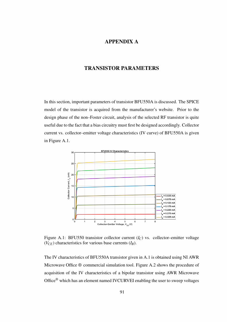
APPENDIX A
TRANSISTOR PARAMETERS
In this section, important parameters of transistor BFU550A is discussed. The SPICE
model of the transistor is acquired from the manufacturer’s website. Prior to the
design phase of the non–Foster circuit, analysis of the selected RF transistor is quite
useful due to the fact that a bias circuitry must first be designed accordingly. Collector
current vs. collector–emitter voltage characteristics (IV curve) of BFU550A is given
in Figure A.1.
Figure A.1: BFU550 transistor collector current (IC) vs. collector–emitter voltage(VCE) characteristics for various base currents (IB).
The IV characteristics of BFU550A transistor given in A.1 is obtained using NI AWR
Microwave Office ® commercial simulation tool. Figure A.2 shows the procedure of
acquisition of the IV characteristics of a bipolar transistor using AWR Microwave
Office® which has an element named IVCURVEI enabling the user to sweep voltages
91

and currents to plot the IV curve.
Figure A.2: Implementation of IVCURVEI element of AWR Microwave Office® soft-ware for the characterization of BFU550A transistor.
Another important transistor parameter is the transistor β : DC current gain (hFE).
Similar to the analysis of IV characteristics, it can also be characterized using the
element IVCURVEI of AWR Microwave Office®. Figure A.3 shows the results for
different collector–emitter voltages (VCE) and collector currents (IC). The transistor β
increases as the collector–emitter voltage increases; however, an increase in collector
current has an adversary effect on the transistor β . In that case, while designing the
bias circuit, one must find a compromise for transistor β and transition frequency of
the transistor fT . The SPICE model of BFU550A based on a Gummel–Poon device
includes the parasitic effects of the transistor packaging (3–pin SOT23). Table A.1
shows the parasitic model values for BFU550A transistor.
The SPICE model of transistor BFU550A is given as follows:
.MODEL BFU550A NPN
+ ( IS=1.1915e-016 BF=133.81 NF=1 VAF=183.69 IKF=0.4212
+ ISE=1.49e-013 NE=2.5 BR=0.51249 NR=1 VAR=2.4 IKR=0.05625
+ ISC=1.1915e-016 NC=1.1 RB=0.7 IRB=0.04463 RBM=0.4 RE=0.36
+ RC=0.54 CJE=8.434e-013 VJE=0.95 MJE=0.33533 CJC=1.236e-013
+ VJC=0.72 MJC=0.31844 XCJC=0.5 FC=0.85 TF=1.004e-011 XTF=10
+ VTF=1 ITF=0.07092 PTF=0 TR=0 KF=1.0967e-010 AF=2 MJS=0.33 VJS=0.75 )
92
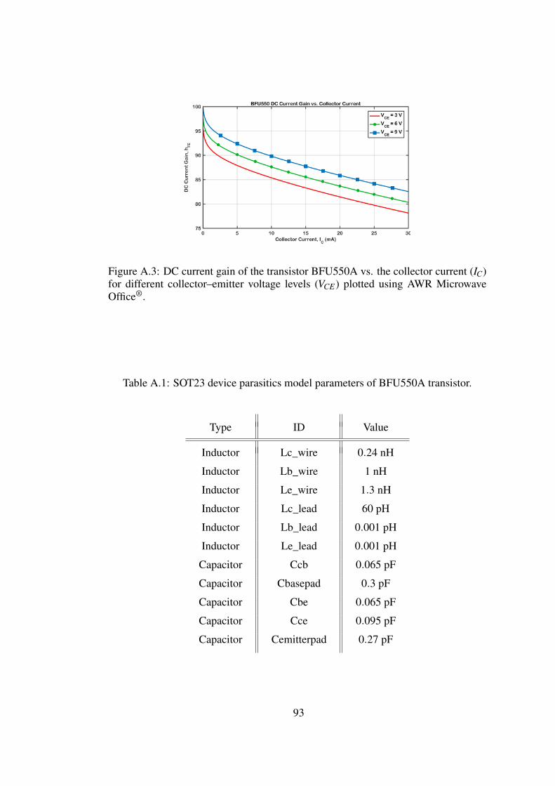
Figure A.3: DC current gain of the transistor BFU550A vs. the collector current (IC)for different collector–emitter voltage levels (VCE) plotted using AWR MicrowaveOffice®.
Table A.1: SOT23 device parasitics model parameters of BFU550A transistor.
Type ID Value
Inductor Lc_wire 0.24 nH
Inductor Lb_wire 1 nH
Inductor Le_wire 1.3 nH
Inductor Lc_lead 60 pH
Inductor Lb_lead 0.001 pH
Inductor Le_lead 0.001 pH
Capacitor Ccb 0.065 pF
Capacitor Cbasepad 0.3 pF
Capacitor Cbe 0.065 pF
Capacitor Cce 0.095 pF
Capacitor Cemitterpad 0.27 pF
93

94
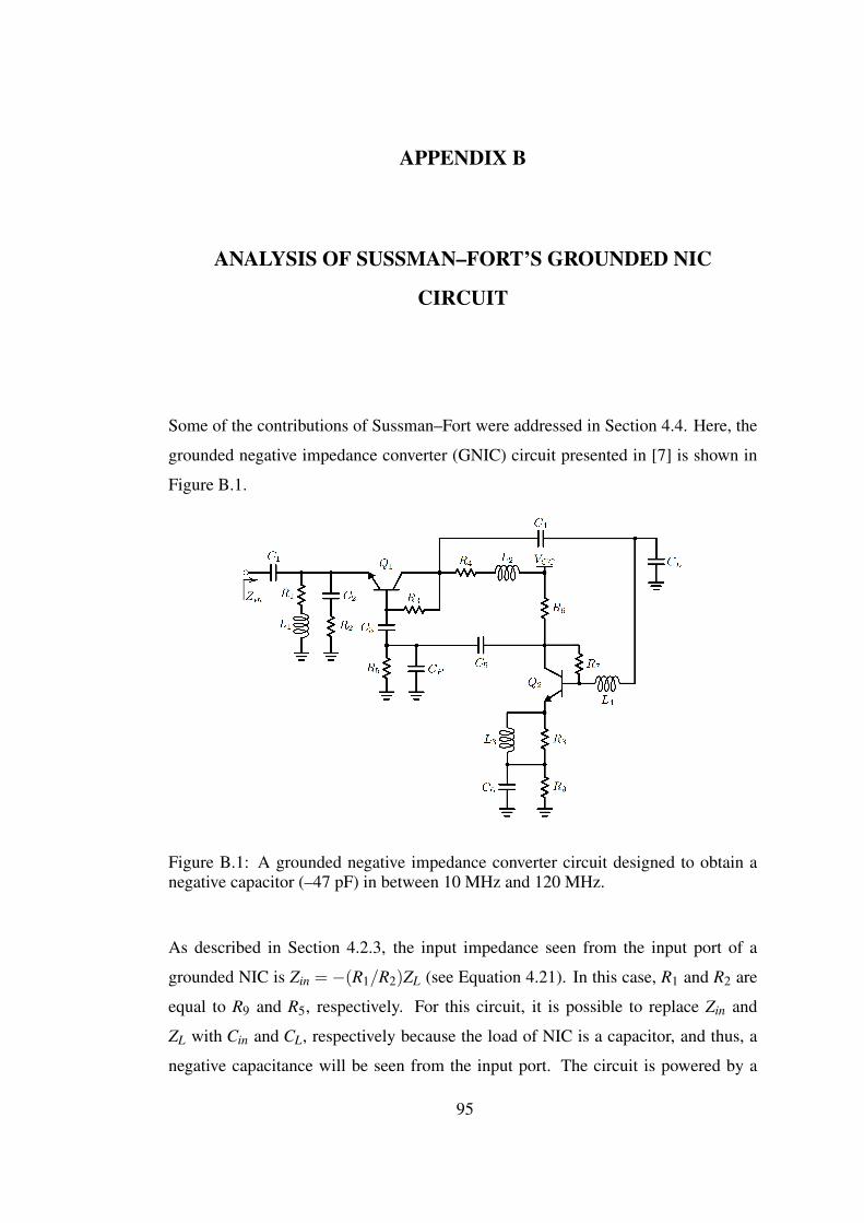
APPENDIX B
ANALYSIS OF SUSSMAN–FORT’S GROUNDED NIC
CIRCUIT
Some of the contributions of Sussman–Fort were addressed in Section 4.4. Here, the
grounded negative impedance converter (GNIC) circuit presented in [7] is shown in
Figure B.1.
Figure B.1: A grounded negative impedance converter circuit designed to obtain anegative capacitor (–47 pF) in between 10 MHz and 120 MHz.
As described in Section 4.2.3, the input impedance seen from the input port of a
grounded NIC is Zin = −(R1/R2)ZL (see Equation 4.21). In this case, R1 and R2 are
equal to R9 and R5, respectively. For this circuit, it is possible to replace Zin and
ZL with Cin and CL, respectively because the load of NIC is a capacitor, and thus, a
negative capacitance will be seen from the input port. The circuit is powered by a
95
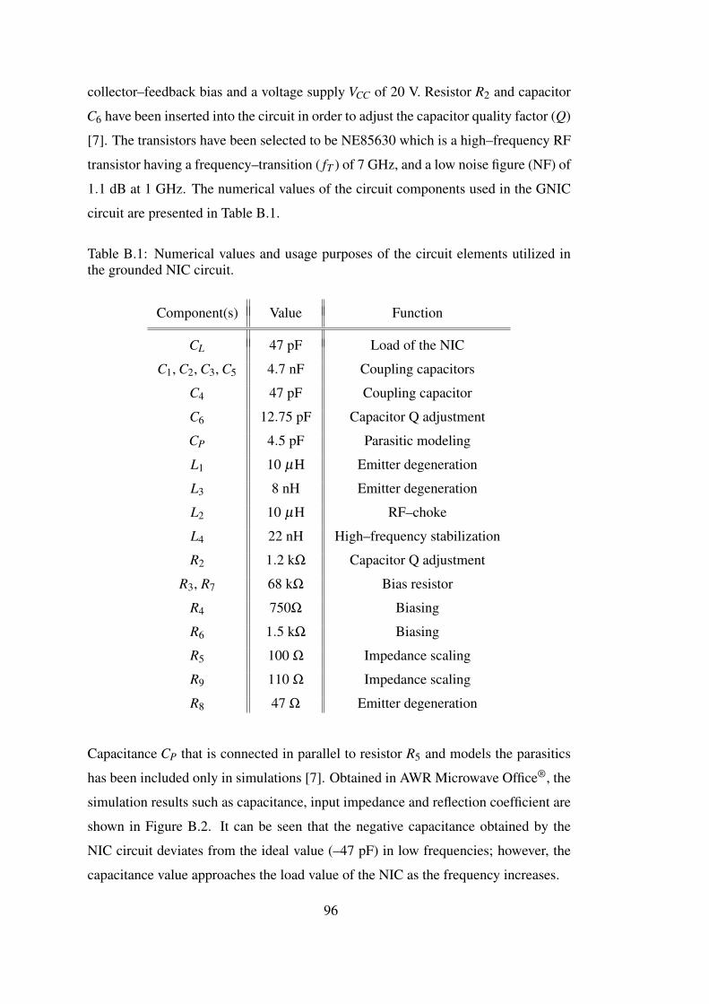
collector–feedback bias and a voltage supply VCC of 20 V. Resistor R2 and capacitor
C6 have been inserted into the circuit in order to adjust the capacitor quality factor (Q)
[7]. The transistors have been selected to be NE85630 which is a high–frequency RF
transistor having a frequency–transition ( fT ) of 7 GHz, and a low noise figure (NF) of
1.1 dB at 1 GHz. The numerical values of the circuit components used in the GNIC
circuit are presented in Table B.1.
Table B.1: Numerical values and usage purposes of the circuit elements utilized inthe grounded NIC circuit.
Component(s) Value Function
CL 47 pF Load of the NIC
C1, C2, C3, C5 4.7 nF Coupling capacitors
C4 47 pF Coupling capacitor
C6 12.75 pF Capacitor Q adjustment
CP 4.5 pF Parasitic modeling
L1 10 µH Emitter degeneration
L3 8 nH Emitter degeneration
L2 10 µH RF–choke
L4 22 nH High–frequency stabilization
R2 1.2 kΩ Capacitor Q adjustment
R3, R7 68 kΩ Bias resistor
R4 750Ω Biasing
R6 1.5 kΩ Biasing
R5 100 Ω Impedance scaling
R9 110 Ω Impedance scaling
R8 47 Ω Emitter degeneration
Capacitance CP that is connected in parallel to resistor R5 and models the parasitics
has been included only in simulations [7]. Obtained in AWR Microwave Office®, the
simulation results such as capacitance, input impedance and reflection coefficient are
shown in Figure B.2. It can be seen that the negative capacitance obtained by the
NIC circuit deviates from the ideal value (–47 pF) in low frequencies; however, the
capacitance value approaches the load value of the NIC as the frequency increases.
96
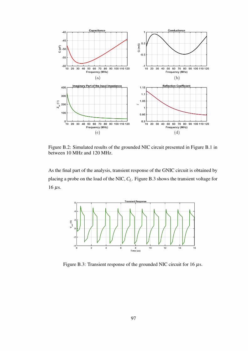
Figure B.2: Simulated results of the grounded NIC circuit presented in Figure B.1 inbetween 10 MHz and 120 MHz.
As the final part of the analysis, transient response of the GNIC circuit is obtained by
placing a probe on the load of the NIC, CL. Figure B.3 shows the transient voltage for
16 µs.
Figure B.3: Transient response of the grounded NIC circuit for 16 µs.
97