passive led driver compatible with rapid-start ballast
TRANSCRIPT

3694 IEEE TRANSACTIONS ON POWER ELECTRONICS, VOL. 26, NO. 12, DECEMBER 2011
Robust Passive LED Driver Compatible WithConventional Rapid-Start Ballast
Byunghun Lee, Member, IEEE, Hyunjae Kim, Student Member, IEEE, and Chuntaek Rim, Member, IEEE
Abstract—In this paper, a new LED fluorescent driver compat-ible with a rapid-start ballast is proposed. Using a compensationcircuit composed of passive elements, a new LED fluorescent driverhaving highly reliable and robust characteristics was developed.This driver can prevent the fire problem that arose in conventionalLED fluorescent switching power supplies. The design principleand architecture of the proposed LED driver was explained, andits feasibility was confirmed by simulations and experiments.
Index Terms—Compensation circuit, LED driver, fluorescent,rapid-start ballast.
I. INTRODUCTION
FOR several decades, fluorescent lamps have been widelyused in industrial, commercial, and institutional interior
lighting applications. However, the global movement to reduceCO2 emissions with greater energy efficiency has affected thedevelopment of new energy-efficient lighting devices such asLED devices [1], [2]. LEDs currently being commercializedhave a long lifetime commonly longer than 50 000 h; hence,they are rapidly replacing conventional fluorescent lamps inmany areas [3]. Recently, several countries in Europe as well asAustralia, several states in the U.S., and Japan have prohibitedthe sales of fluorescent lamps to foster local LED industriesand concentrate on expanding the LED markets. In addition,governments have made it mandatory to use high-efficiencylighting devices [4]–[6]. Among these countries, Japan has thelargest share of the use of fluorescent lighting devices [7] in theworld; hence, the replacement of them with LED devices is anespecially important issue.
The replacement of conventional fluorescent lamps with LEDdevices, however, has been impeded by the existing ballasts influorescent lighting devices. The ballast implemented in con-ventional fluorescent lamps, as shown in Fig. 1(a), was used toprovide the starting and operating lamp voltage and to limit thelamp current due to the negative V–I characteristic of a fluores-cent lamp [8]. Therefore, the ballast of a fluorescent lamp is notdirectly suitable for the driver of an LED device.
Manuscript received January 15, 2011; revised April 7, 2011; accepted April29, 2011. Date of current version December 6, 2011. This paper was presentedin part at the IEEE Energy Conversion Congress and Exposition (ECCE)-ASIAin 2011. Recommended for publication by Associate Editor J. M. Alonso.
B. Lee and C. Rim are with the Department of Nuclear and Quantum En-gineering, Korea Advanced Institute of Technology, Daejeon 305-755, Korea(e-mail: [email protected]; [email protected]).
H. Kim is with the Department of Electrical Engineering, Korea AdvancedInstitute of Technology, Daejeon 305-701, Korea (e-mail: [email protected]).
Digital Object Identifier 10.1109/TPEL.2011.2153875
Fig. 1. Configurations of power lighting lamps and their drivers. (a) Conven-tional fluorescent lamp with a ballast. (b) LED lamp with an SMPS. (c) LEDlamp with an SMPS plugging into the existing ballast.
The ballasts for fluorescent lamps in present use can be clas-sified into three types: a preheated magnetic ballast, a rapid-startballast, and an electronic ballast with a switch mode power sup-ply (SMPS) [9]. It is estimated that about 85% of all ballastsin Japan are the rapid-start ballast, which is heavy and robustlymounted deep inside the ceiling. Although several LED driverswith SMPSs have been proposed to replace the existing rapid-start ballasts, as shown in Fig. 1(b) [10]–[14], they are notwidespread at present because it is very difficult and expensiveto separate the rapid-start ballast from the ceiling. This addi-tional work incurs a high cost.
An economic and practical solution may be to leave the ro-bust rapid-start ballast alone and to reuse it as part of an LEDdriver. From the consumer’s point of view, this type is attractiveand user friendly. As a candidate solution, a tubular LED de-vice equipped with an SMPS has been suggested, featuring highefficiency, well-regulated power, and good stability [15]–[20].This LED device can simply be plugged into existing fluores-cent lighting device without any additional treatment, as shownin Fig. 1(c) [21], [22]. However, this type has also not gainedmarket credibility due to the occasional fires that arise insidethe rapid-start ballast. The cause of these fires has not yetclearly been verified. Furthermore, the SMPS usually suffersfrom switching harmonics and electro magnetic interference(EMI), relatively shorter lifetime than an LED lamp, and com-plexity caused by control integrated circuit [23], [24].
0885-8993/$26.00 © 2011 IEEE

LEE et al.: ROBUST PASSIVE LED DRIVER COMPATIBLE WITH CONVENTIONAL RAPID-START BALLAST 3695
Fig. 2. Characterization of a conventional rapid-start ballast. (a) Circuits fora rapid-start ballast with a fluorescent lamp. (b) Characteristic of a saturabletransformer in the rapid-start ballast.
In this paper, a reliable and extremely long endurance passive-type LED driver compatible with the rapid-start ballast is pro-posed. This passive-type LED driver has advantages such ashigh robustness, high efficiency, low harmonic distortions, anda long lifetime. Since most materials used in the proposed LEDdriver can be recyclable, it is more eco-friendly than an SMPS.It is also verified that the cause of the fires in an LED driver withan SMPS is the large dc input capacitor of the SMPS, which candestroy the capacitor of the ballast due to excessive initial reso-nant voltage [25]. The proposed ballast was analyzed by phasortransformation theory [26]–[29] and verified by simulations andexperiments.
II. OVERVIEW OF RAPID-START BALLAST
A rapid-start ballast includes a saturable transformer withsecondary windings to provide filament heaters with currentsand capacitors for power factor correction, as shown in Fig. 2(a).The transformer, equivalently a saturable reactor, is saturated ata large secondary current, as shown in Fig. 2(b). The turn ratioof the transformer n starts to decrease for the ballast current Ibf
and becomes fully saturated at the current Ibs . As the supplyvoltage is applied, the saturable reactor is initially unsaturated,i.e., n = nf , due to a small current. It can provide high voltageto the fluorescent lamp while providing heater currents so as to
turn ON the fluorescent lamp. n1 and n2 represent the numberof turns of the primary coil and the secondary coil, respectively.
Once the fluorescent lamp is turned ON, the saturable reac-tor becomes saturated, i.e., n = ns , and the voltage applied tothe fluorescent lamp remains constantly low. The current andvoltage of the fluorescent lamp are relatively unchanged regard-less of the supply voltage due to the regulating capability ofthe saturable reactor. The internal capacitance Cb is selected soas to offset the reactive power of the magnetizing inductanceof the saturable reactor, allowing the input power factor of theconventional fluorescent lamp to be close to unity.
III. PASSIVE COMPENSATION CIRCUIT DESIGN: STEADY STATE
A. Overall Design Requirement
When replacing a conventional fluorescent lamp with an LEDdevice using an additional compensation circuit while maintain-ing the existing rapid-start ballast, passive circuit elements aremostly preferred to active switches because the lifetime of thecircuit elements should equal that of the LED lamps. The com-pensation circuit should meet several design requirements, suchas the output power, input power factor, and total harmonicdistortion (THD).
As LED lamps show better luminance efficiency than conven-tional fluorescent lamps, the entire LED driver should provideless power with LED arrays for the same amount of luminancenoted with fluorescent lamps [30]. For a traditional 40 W flu-orescent lamp with around 80 lm/W [31], a 20 W LED lampcomposed of 150 lm/W LED chips can give similar luminanceby virtue of recent advanced LED technology. This reducedpower changes the input power factor of the rapid-start ballastfrom unity, as the saturable transformer is not fully saturated bythe reduced secondary current. Furthermore, severe harmonicdistortion may appear in the source current given that the bal-last deviates from resonance due to the unsaturated transformer.Therefore, an additional compensation circuit should compen-sate not only the variation of the input power factor but also thevariation of the resonant frequency.
B. Compensation Circuit Configuration
To meet the design requirements as stated in Section III-A,a passive compensation circuit composed of inductors and acapacitor is proposed as an interface between the existing rapid-start ballast and a tabular LED lamp, as shown in Fig. 3(a).When replacing a fluorescent lamp with an LED lamp withoutthis interface circuit, the input power factor of the rapid-startballast lags because the capacitive current decreases due to thereduced output power of the LED lamp, i.e., 20 W.
To make the input power factor of the proposed LED driver,which is composed of a conventional rapid-start ballast and acompensation circuit, reach unity, the compensation capacitorCc should be connected in parallel with the bridge diode andLED arrays to provide additional leading reactive power, asshown in Fig. 3(a). The compensation inductors Lc1 , Lc2 , Lc 3 ,and Lc 4 should be added in series to maintain the same resonantfrequency as the original rapid-start ballast for the conventional

3696 IEEE TRANSACTIONS ON POWER ELECTRONICS, VOL. 26, NO. 12, DECEMBER 2011
Fig. 3. Proposed passive LED driver with an LED lamp. (a) Proposed LEDdriver using a compensation circuit. (b) Simplified equivalent circuit. (c) Mea-sured inductances Ll and Lm versus the source voltage.
fluorescent. To connect the LED lamp freely regardless of thepolarity of the rapid-start ballast, four inductors, instead of aninductor, with equal values of inductance should be used.
For simplicity, Fig. 3(a) is represented as a simple equivalentcircuit, as shown in Fig. 3(b). Here, Lm is the equivalent in-ductance from the primary coil to the secondary coil includingthe magnetizing inductance, and Ll is the equivalent inductancefrom the secondary coil to the primary coil including the leakageinductance of the transformer. The inductances Ll and Lm varywith the input voltage, as shown in Fig. 3(c), due to the non-linearity of the rapid-start ballast. Rs is the equivalent parasiticserial resistor inside the rapid-start ballast. The capacitor Cz isrelatively small, and the parallel resistor Rb is large enough sothat they can be negligible in the following simplified equivalentcircuit. However, Rc , which is the equivalent parasitic resistorof the compensation inductor, should be included. Note thatthe heater voltage provided by secondary windings is merely afew volts compared to the large output voltage; hence, the cur-rent through each inductor is around half of the current throughLc which is the ballast current Ib . The total energy of these
Fig. 4. Equivalent circuit removing the ideal transformer in Fig. 3(b).
inductors Etotal is equal to that of an equivalent inductor ELc
which is defined as follows:
Lc = Lc1 = Lc2 = Lc3 = Lc4 (1)
Etotal ≡ 4 × ELc1 =12Lc1
(Ib
2
)2
+12Lc2
(Ib
2
)2
+12Lc3
(Ib
2
)2
+12Lc4
(Ib
2
)2
=12Lc1I
2b =
12LcI
2b ≡ ELc. (2)
Therefore, the LED driver regardless of the polarity of the ballastcan be implemented without any increase in the capacity ofinductor. The LED lamp, which is a combination of a bridgediode rectifier with a dc capacitor and the LED arrays, can beexpressed as the equivalent resistance RL in the steady state [27],as shown in Fig. 3.
C. Constraints for a Compensation Circuit
Fig. 4 represents the source-side equivalent circuit removingthe saturable transformer in Fig. 3(b). The inductance Ls is thesum of Ll and Lc , while Im and Ib are the currents flowingthrough Lm and Ls , respectively.
To determine the values of Lc and Cc in the compensationcircuit, the following four requirements are established:
Im {Im + (1 + n)Is}=Im{
Vs ·(
1jωLm
+1
Z1 + Z2
)}=0
(3)
PL ≡ V 2c
RL= (1 + n)2 V 2
s
RL
∣∣∣∣ Z2
Z1 + Z2
∣∣∣∣2∼= 20W (4)
(1 + n)Ib =Vs
Z1 + Z2(5)
n = f(Ib) (6)
where Z1 and Z2 are defined as follows:
Z1 =Rs + Rc
(1 + n)2 +jωLs
(1 + n)2 +1
jω(1 + n)2Cb(7)
Z2 =RL
(1 + n)2 //1
jω(1 + n)2Cc. (8)
The condition for the input power factor to be unity is shownin (3), allowing the capacitive current through Cb to offset theinductive current through Lm and the total reactive current tobecome zero. The condition for the same brightness from a 40 Wfluorescent lamp as from an LED lamp is around 20 W, as shown

LEE et al.: ROBUST PASSIVE LED DRIVER COMPATIBLE WITH CONVENTIONAL RAPID-START BALLAST 3697
TABLE IPARAMETERS OF RAPID-START BALLAST
Fig. 5. Measured turn ratio of the ballast versus the ballast current.
in (4). The ballast current Ib through Ls can be determined by(5), and the turn ratio of the ballast can be defined by a functionof Ib , as shown in (6), which is depicted in Fig. 2(b). Given thatIm is independent of the turn ratio n, the variation in the turnratio changes the capacitive current Ib and the mismatch of thereactive currents between Ib and Im deteriorates the input powerfactor. At this point, the values of n, Lc , Cc , and RL shouldbe determined from (3) to (6), where we have five unknownvariables including Ib but have only four equations. One moreequation, which is the last constraint of the compensation circuit,is related to the THD; however, it is not entirely possible tocharacterize it until we have measurements. Therefore, it is notstraightforward to determine the circuit parameters in theory;hence, they should be finally tuned by experiments consideringthe uncertainties of n and the circuit parameters of the ballast.
D. Parameter Determination of a Compensation Circuit
The selected rapid-start ballast for the experiments was FRH-40128B, operating at 100 V with a 60 Hz input voltage for a44 W fluorescent lamp. The parameters of the ballast were char-acterized by direct measurements and experimental estimations,as shown in Table I. The turn-ratio variation of the ballast as afunction of the ballast current Ib was measured, as shown inFig. 5. The linear fitting of the curve between 0.10 and 0.23 Awas performed to characterize (6), as follows:
n + 1 = a |Ib | + b = −1.0 |Ib | + 1.95. (9)
Fig. 6. Calculated load power PL versus the turn ratio n.
To determine the parameters of the compensation circuit with(3)–(6), the value of n was set first. Cc could then be expressedby the variable RL in each case, whereas Lc can be expressed bythe variables RL and Cc using (3), (5), (6), and (9), as follows:
Cc =1
ω RL
√RL
α − (Rs + Rc)− 1 (10)
Lc =β
ω+
1ω2Cb
+R2
LC2c
1 + ω2R2LC2
c
− Ll. (11)
Here, both α and β can be defined as a function of n, respec-tively, as follows:
α =
√(n + 1)2a2V 2
s
{b − (n + 1)}2 −(
a2V 2s
ωLm{b − (n + 1)}2
)2
(12)
β = − a2V 2s
ωLm{b − (n + 1)}2 . (13)
The load power PL of (4) can be determined through thefollowing equation:
PL = (1 + n)2 V 2s
RL
∣∣∣∣ Z2
Z1 + Z2
∣∣∣∣2
=(n + 1)2V 2
s R2L
(α2 + β2)(1 + ω2R2LC2
c )
={α − (Rs + Rc)}(n + 1)2V 2
s
(α2 + β2). (14)
Because both α and β are functions of n, the load power PL isa function of only n regardless of RL , Lc , or Cc . The plot of PL
versus n is shown in Fig. 6. For the LED driver with 20 W ofoutput power, n was found to be 0.725 as shown in Fig. 6. Thus,the values of Cc and Lc are obtained from (10) and (11) providedthat the value of RL is given. Fig. 7 shows plots of both Lc andCc with respect to RL in the case of n = 0.725. Considering thesize of the inductor and the THD, which drastically increasesfor a small amount of inductance, the load RL should be setat approximately 800 Ω. The Lc and Cc values are, therefore,determined as 0.5 H and 3.2 μF, respectively.

3698 IEEE TRANSACTIONS ON POWER ELECTRONICS, VOL. 26, NO. 12, DECEMBER 2011
Fig. 7. Calculated compensation circuits Cc and Lc versus RL at n = 0.725.
Fig. 8. Measured I–V characteristic of an ET-5050W-3F1W LED for theexperiments.
TABLE IIPOWER MEASUREMENT RESULT
The ET-5050W-3F1W LED used in this paper has the prop-erty of a forward voltage drop of 3.1 V and a dynamic resistanceof 6.6 Ω, as shown in Fig. 8, where the I–V characteristic curveof an LED was measured for experiments. The luminous effi-cacy of the LED chip is 150 lm/W. Three parallel LED arrayscomposed of 45–48 LEDs each were implemented to give thepresumed value of 800 Ω, which can be determined by the ra-tio of the LED voltage and the LED current experimentally, asshown in Table II.
Fig. 9. Measured source voltage/current and output voltage waveforms for thecalculated Lc = 0.50 H and Cc = 3.2 μF.
IV. EXPERIMENTAL VERIFICATION FOR STEADY STATE
A. Optimized Compensation Circuit by Experiment
The proposed passive LED driver design was verified byexperiments based on the parameters in the previous sectionfirst. Fig. 9 shows the measured waveforms of the input voltageand current and the output voltage for the case of Lc = 0.50 Hand Cc = 3.20 μF, respectively. The power was measured by aWT1600 digital power meter, and the result is summarized inTable II. Due to the uncertainty of n as well as the nonlinearityin the rapid-start ballast, the experimental results are not exactlythe same as the calculated results, i.e., the measured outputpower was 18.4 W instead of the designed value of 20.0 W.
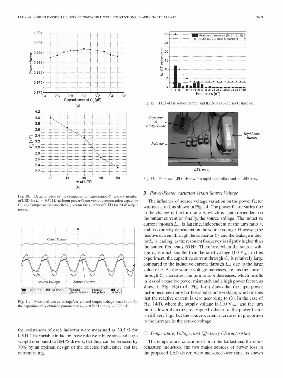
The optimal Lc and Cc values should be, therefore, tunedby experiments empirically, as shown in the third column ofTable II. The power-factor variation was widely explored overthe capacitance Cc , as shown in Fig. 10(a), where the powerfactor reaches its highest value of 0.992 when Cc = 3.0 μFinstead of Cc = 3.2 μF. The required capacitance Cc was alsosought to guarantee 20 W of output power for different numbersof LED arrays, as shown in Fig. 10(b), where the number ofLEDs was determined to be 47 when Cc = 3.0 μF. The measuredwaveforms are shown in Fig. 11 for the optimal values of Lc =0.50 H and Cc = 3.0 μF with 47 LEDs, where no severe THDis observed.
Another choice of Lc and Cc could be 0.64 H and 3.33 μF,respectively, as shown in the fourth column of Table II. Theoutput power was measured as precisely 20.0 W, whereas it was21.3 W for the former case. It also showed a high power factorwith 45 LEDs and good THD characteristics; however, a largervalue of the inductance Lc will likely be an obstacle if attemptingto implement this LED driver; hence, these parameters wereexcluded from further consideration.
The THD in the source current of the optimized LED driverwas also measured by WT1600, as shown in Fig. 12. Consider-ing that the THD of the source current was 13.1% at 60 Hz ofthe source voltage containing 4.75% THD, the optimized LEDdriver meets IEC61000-3-2 class C standard.
The proposed LED driver together with an LED lamp is dis-played in Fig. 13, where the variable inductors were manufac-tured to modulate their inductances for the experiments and
LEE et al.: ROBUST PASSIVE LED DRIVER COMPATIBLE WITH CONVENTIONAL RAPID-START BALLAST 3699
Fig. 10. Determination of the compensation capacitance Cc and the numberof LED for Lc = 0.50 H. (a) Input power factor versus compensation capacitorCc . (b) Compensation capacitor Cc versus the number of LED for 20 W outputpower.
Fig. 11. Measured source voltage/current and output voltage waveforms forthe experimentally obtained parameters: Lc = 0.50 H and Cc = 3.00 μF.
the resistances of each inductor were measured as 30.5 Ω for0.5 H. The variable inductors have relatively huge size and largeweight compared to SMPS drivers, but they can be reduced by70% by an optimal design of the selected inductance and thecurrent rating.
Fig. 12 THD of the source current and IEC61000-3-2 class C standard.
Fig. 13. Proposed LED driver with a rapid-start ballast and an LED array.
B. Power-Factor Variation Versus Source Voltage
The influence of source voltage variation on the power factorwas measured, as shown in Fig. 14. The power factor varies dueto the change in the turn ratio n, which is again dependent onthe output current or, finally, the source voltage. The inductivecurrent through Lm is lagging, independent of the turn ratio n,and it is directly dependent on the source voltage. However, thereactive current through the capacitor Cb and the leakage induc-tor Ll is leading, as the resonant frequency is slightly higher thanthe source frequency 60 Hz. Therefore, when the source volt-age Vs is much smaller than the rated voltage 100 Vrms in thisexperiment, the capacitive current through Cb is relatively largecompared to the inductive current through Lm due to the largevalue of n. As the source voltage increases, i.e., as the currentthrough Cb increases, the turn ratio n decreases, which resultsin less of a reactive power mismatch and a high power factor, asshown in Fig. 14(a)–(d). Fig. 14(e) shows that the input powerfactor becomes unity for the rated source voltage, which meansthat the reactive current is zero according to (3). In the case ofFig. 14(f), where the supply voltage is 110 Vrms and the turnratio is lower than the predesigned value of n, the power factoris still very high but the source current increases in proportionto the increase in the source voltage.
C. Temperature, Voltage, and Efficiency Characteristics
The temperature variations of both the ballast and the com-pensation inductors, the two major sources of power loss inthe proposed LED driver, were measured over time, as shown

3700 IEEE TRANSACTIONS ON POWER ELECTRONICS, VOL. 26, NO. 12, DECEMBER 2011
Fig. 14. Measured power-factor variation of the ballast versus the sourcevoltage. (a) 30 Vrm s , n = 0.87. (b) 50 Vrm s , n = 0.84. (c) 70 Vrm s , n = 0.80.(d) 90 Vrm s , n = 0.70. (e) 100 Vrm s , n = 0.60. (f) 110 Vrm s , n = 0.48.
Fig. 15. Measured temperature variations of the ballast and the compensationinductors for heavy load conditions: 120 Vrm s source voltage and 30 W outputpower.
in Fig. 15. The LED driver was operated intentionally undera 120 Vrms source voltage and at a 30 W output power, simu-lating harsh conditions. This experiment demonstrated that thetemperature variations of both the ballast and the inductors areacceptable.
Fig. 16 shows the measured output power of the LED driverfor different source voltages. The power varies from 18 to 25 Wunder ±5 V variation of the source voltage. Although the pro-posed LED driver does not have a high-output-power regulationcapability as compared to the LED driver with an SMPS, it isquite acceptable for many practical applications.
Fig. 16. Measured output power of the LED driver versus the source voltage.
The efficiency of the proposed LED driver including theballast was measured as 72.9%, where the source power was29.13 W and the output power was 21.25 W. Because the bal-last dissipates 5.62 W of power in the case, the efficiency ofthe compensation circuit excluding the ballast is as high as90.4%.
V. TRANSIENT STATE ANALYSIS AND
EXPERIMENTAL VERIFICATION
Transient state analyses for the LED device with an SMPS[15]–[20] and the proposed passive LED driver are essential toidentify the transient peak voltage of the capacitor Cb inside therapid-start ballast. The capacitor Cb could be destroyed duringthe power-ON switching period, which is presumably the causeof the aforementioned fires that have occurred in the LED de-vice with an SMPS. In practical conditions, the LED driverswith the rapid-start ballast can be turned ON and turned OFFswiftly and randomly due to the imperfect electric switch andsource voltage variation, as shown in Fig. 24. The input voltageof the LED drivers may fluctuate from zero to the rated sourcevoltage 100 V or vice versa for a few cycles, and the induc-tances of the ballast change drastically according to the sourcevoltage, as shown in Fig. 3(c). To deal with this, severe nonlin-earity appearing in the harsh operating conditions is crucial fora robust LED driver design. For simplicity, the operations of theLED drivers with the rapid-start ballast can be separated intotwo regions according to the resonant frequency determined bythe capacitance Cb and related series inductance: the resonantregion and the nonresonant region. It is identified that the res-onant region corresponds to the source voltage range from 10to 30 V and the nonresonant region is over 30 V of the sourcevoltage. In the resonant region, transient-state analyses wereperformed by both the experiment and the powerful tool for acanalyses, phasor transformation [26]–[29]. In the nonresonantregion, only the experimental results were demonstrated for thetransient analyses due to the nonlinearity of the rapid-start bal-last as well as the complexity of the phasor transformation inthe nonresonant case.

LEE et al.: ROBUST PASSIVE LED DRIVER COMPATIBLE WITH CONVENTIONAL RAPID-START BALLAST 3701
Fig. 17. Derivation of a worst case scenario for an LED device with SMPS.(a) Simplified circuit of the LED driver with SMPS focusing on resonant tank.(b) Phasor-transformed circuit in (a). (c) Worst case circuit for the transientanalysis. (d) Equivalent circuit eliminating the transformer in (c).
A. LED Device With an SMPS in the Resonant Region
The LED device with an SMPS, which contains the rapid-start ballast and a large dc input capacitor Co in its SMPS, canbe simplified as shown in Fig. 17(a). The saturable transformerand the voltage source are substituted with an equivalent voltage,and the other part of the SMPS except the dc input capacitor isregarded as a resistor Ro , for simplicity.
Given that the bridge diode is equivalent to a time-varyingtransformer [28] in general and because an LC resonant tankis equivalent to a circuit composed of an equivalent inductorand an imaginary resistor in the phasor-transformed domain[27], this setup can be drawn as shown in Fig. 17(b), wherethe equivalent inductor and imaginary resistors in the resonantregion are expressed as follows:
Leq = Ll
[1 +
(ωr
ωs
)2]∼= 2Ll for ωs
∼= ωr (15)
Xeq = ωsLl
[1 −
(ωr
ωs
)2]∼= 0 for ωs
∼= ωr . (16)
Here, ωs is the source frequency and ωr is the resonant fre-quency as determined by Ll and Cb . ωr is very close to ωr
in the resonant region, because the equivalent inductance Ll
is about 1.3 H as shown in Fig. 3(c). For example, when thesource voltage is 10 Vrms , the frequencies become ωs = 60 Hzand ωr = 64 Hz, respectively, for our experiment. To find themaximum initial resonant current in the worst case, two approx-imations are added on the circuit in Fig. 17(b); they neglectthe internal resistance of the rapid-start ballast Rs and diminishthe imaginary resistor jXeq for ωs
∼= ωr , as shown in (16). Byapplying the approximations, Fig. 17(b) is simplified as shownin Fig. 17(c), where Leq is 2Ll , as shown in (15). Finally, thephasor-transformed circuit removing the transformer is shownin Fig. 17(d). The turn ratio of the equivalent transformer of thebridge rectifier α is 0.90 [27]. Therefore, the peak resonant tankcurrent in the worst case and assuming no output resistance Ro
can be calculated from Fig. 17(d) as follows, where Vp refers tothe peak of the source rms voltage (1+n)Vs :
IL,p∼=
√Co
2α2Ll· Vp =
(1 + n)Vs
√2
α
√Co
2Ll
=(1 + n)Vs
α
√Co
Ll. (17)
Using (17), the peak voltage across the capacitor Cb can becalculated as follows:
VC b,p = IL,p · 1ω Cb
=(1 + n)Vs
α ω Cb
√Co
Ll. (18)
To verify the validity of the phasor transformation first,PSIM simulations were implemented for the original circuitin Fig. 17(a) and for the approximated phasor-transformed cir-cuit eliminating the transformer in Fig. 17(d). The simulationparameters used for this purpose were Vs = 10 Vrms , Ll = 1.3 H,Cb = 5.4 μF, and Ro = 200 Ω. The simulation parameter valueof Cb was set to 5.4 μF to equalize the source frequency andresonant frequency, i.e., 60 Hz, which would give us the resultsfor the worst case scenario. The simulations were performedfor different values of the capacitor Co . It was verified that theenvelope of ib is identical to that of ib , as shown in Fig. 18(a)and (b). However, some discrepancy is observable in Fig. 18(c),where Co is as large as 1000 μF; therefore, the diode recti-fier is operating in the discontinuous conduction mode (DCM).This problem can be simply solved by inserting a diode intothe inductor of the phasor-transformed circuit to simulate theoperation in the DCM, as shown in Fig. 19, where the envelopeof ib is identical to that of ib again. It is clear that the phasortransformation can be used for the verification of the transientbehavior, where the resonant circuit of the rapid-start ballast inthe resonant region and the large dc input capacitor of the SMPSare involved.
The calculated results from (18) reflecting the variations ofthe turn ratio n according to Ib and the experiment results ofVcb,p for different values of Co are shown in Fig. 20. The figure

3702 IEEE TRANSACTIONS ON POWER ELECTRONICS, VOL. 26, NO. 12, DECEMBER 2011
Fig. 18. Simulation waveforms of ib and ib , where Co is (a) 100 μF,(b) 400 μF, and (c) 1000 μF.
Fig. 19. Simulation waveforms of ib and ib considering DCM of dioderectifier, where Co is 1000 μF.
shows that the calculated results and the experiment results forVcb,p are almost the same and that the peak voltage becomes aslarge as 130 V for a large Co even for only the 10 Vrms sourcevoltage. The Vcb,p could reach to several hundred volts when theLED driver with a rapid-start ballast operates in the resonatedregion.
B. Proposed Passive LED Driver in the Resonant Region
There are no significant differences in the transient behaviorsof the LED device with the SMPS and the proposed passiveLED driver in the resonant region, as shown in Fig. 21(a), asthe LC compensation circuit, which is the only difference, doesnot play an important role in the dynamics. In other words,
Fig. 20. Calculated and experiment results of Vcb ,p versus Co for the LEDdevice with an SMPS in the resonant region for 10 Vrm s source voltage.
the dc capacitor of the proposed passive LED driver is moresignificant while operating in the transient state. This physicalinsight is verified in the following equations through a somewhatcomplicated process using phasor transformation.
The time-varying transformer-model-based [28] equivalentcircuit is shown in Fig. 21(b), where Ls is the sum of Ll andLc and the turn ratio of the equivalent transformer of the bridgerectifier is time varying. The internal resistance of the rapid-start ballast Rs , as in the case of the previous LED device withSMPS, is neglected in the following analysis. Applying phasortransformation to the time-varying circuit in Fig. 21(b), a phasor-transformed circuit is obtained, as shown in Fig. 21(c). The LCseries resonant tank in Fig. 21(c) is equivalent to the circuitcomposed of an equivalent inductor and an imaginary resistor;hence, it can be drawn as shown in Fig. 21(d) [27]. Here, ωs isthe input voltage frequency and ω′r is the resonant frequency ofLs and Cb , as follows:
L′eq = Ls
[1 +
(ω′
r
ωs
)2]
(19)
X ′eq = ωsLs
[1 −
(ω′
r
ωs
)2]
. (20)
In Fig. 21(d), Za (s) and Zb (s) are as follows:
Za(s) = sL′eq + jX ′
eq (21)
Zb(s) =1
sCc + jωsCc. (22)
The equivalent circuit of Fig. 21(d) using Thevenin’s theoremand the Laplace transform is shown in Fig. 21(e), where Vth (s)and Zth (s) are as follows:
Vth(s) =(1 + n)Vs(s)
(sL′eq + jX ′
eq)(sCc + jωsCc) + 1(23)
Zth(s) =1
(1/Za(s) + (1/Zb(s)
∼= Za(s)(
1 − Za(s)Zb(s)
)∼= sLT + jXT . (24)

LEE et al.: ROBUST PASSIVE LED DRIVER COMPATIBLE WITH CONVENTIONAL RAPID-START BALLAST 3703
Fig. 21. Derivation of a worst case scenario for the proposed LED driver.(a) Simplified circuit of the proposed passive LED driver. (b) More simplifiedtime-varying equivalent circuit. (c) Phasor-transformed circuit in (b). (d) Systemorder reduction of LC series resonant in (c). (e) Thevenin-equivalent circuit in(d). (f) First-order approximation of the Thevenin circuit.
Here, Zth (s) is calculated after considering the fact that theabsolute magnitude of Zb (s) is much larger than that of Za (s) inthe circuit and that only first-order system response is of greatconcern; hence, LT and XT are as follows:
LT = L′eq + 2L′
eqX′eqωsCc + X ′2
eqCc (25)
XT = X ′2eqωsCc + X ′
eq . (26)
Fig. 22. Calculated and experiment results of Vcb ,p versus Co for the proposedpassive LED driver in the resonant region for 10 Vrm s source voltage.
In Fig. 21(f), it is verified that the proposed passive LEDdriver can also be simplified into the same form as expressed inFig. 17(b). Here, XT is also negligible in the following analysisprocess, as the role of XT is quite small compared to that of LT atresonance [27]. The peak resonant tank current in the worst caseassuming no output resistance Ro can be calculated as follows,where Vth,p refers to the peak of Vth :
ILT ,p =√
Co
α2LT·Vth,p =
√Co
α2LT·√
2Vth =√
2Co
α2LT·Vth
(27)
Vth ∼= Vth(s) |s=0 =(1 + n)Vs
1 − X ′eqωsCc
. (28)
Using Vth of (28), which is the steady-state value of Vth(s) ,the peak voltage across the capacitor Cb can be calculated asfollows:
VC b,p = ILT ,p · 1ω Cb
. (29)
To analyze the transient state of the proposed LED driver inthe resonant region, the experiments were also performed. Theexperiment parameters were used: Vs = 10 Vrms , Ll = 1.3 H,Cb = 4.6 μF, Lc = 0.5 H, Cc = 3.0 μF, Ro = 980 Ω, and Co =47 –300 μF.
Fig. 22 shows the experiment result for Vcb,p and the calcu-lated result using (29) for several dc capacitances Co . As errorsare generated by the simplifications and the approximation pro-cesses, there is some discrepancy between the calculated andthe experiment results; however, considering the complicatednonlinearity of the rapid-start ballast, it is clear that the transientanalyses of the proposed LED driver using the phasor transfor-mation are very useful in the resonant region of the rapid-startballast. The peak voltage Vcb,p becomes as large as 115 V for alarge Co even for the 10 Vrms source voltage on the proposedLED driver.

3704 IEEE TRANSACTIONS ON POWER ELECTRONICS, VOL. 26, NO. 12, DECEMBER 2011
Fig. 23. Experiment results of Vcb ,p versus Co for the LED device with anSMPS in the nonresonant region for 100 Vrm s source voltage.
C. LED Device With an SMPS and Proposed PassiveLED Driver in the Nonresonant Region
In the nonresonant region of the rapid-start ballast, when thesource voltage is larger than 30 Vrms , the rapid-start ballast hasthe equivalent inductance Ll decreased from about 1.3 to 0.5 H,as shown in Fig. 3(c). As a result, the resonant frequencies ωr
and ω′r for the LED device with an SMPS and the proposed
passive LED driver, respectively, become higher and are verydifferent from the source frequency ωs . Transient-state analy-ses using phasor transformation in the nonresonant region arevery complicated and difficult [27], [29]. Therefore, experimentswere carried out to verify the transient peak voltage of the capac-itor Cb during the power-ON switching period. In the case of anLED device with an SMPS, as shown in Fig. 17(a), experimentconditions were as follows: Vs = 100 Vrms , Ro = 2400 Ω, loadpower ≡ 20 W, and Co = 47–300 μF. The experiment resultsof Vcb,p for different values of Co are shown in Fig. 23. Thisresult shows that the peak voltage across Cb increases with theincrease of the value of Co . The dc capacitor used in the SMPSof an LED device typically exceeds a few hundred microfarads,which could result in the large current flow into the dc capacitorduring the initial transient period. Therefore, the large dc capac-itor in the SMPS of an LED device during the initial transientperiod could be considered as a short circuit.
An example of the transient peak voltage of the capacitor Cb
during the power-ON switching period for the proposed LEDdriver in the nonresonant region is shown in Fig. 24, where Vs =100 Vrms , Ro = 980 Ω, load power ≡ 20 W, and Co = 47 μF.
In the nonresonant region, it is identified from the experimentsthat the peak voltage of the capacitor Cb during the power-ONswitching period is dominated by the dc capacitor, whereasthe difference between the LED device with an SMPS and theproposed LED driver is not of great concern.
D. Verifications for the Worst Case of LED Device Withan SMPS and Proposed Passive LED Driver
To find the peak voltage across Cb in the worst of the worstcase, two situations were considered regarding the dc capacitor
Fig. 24. Experiment result of Vcb ,p versus Co for the proposed LED driver inthe nonresonant region for 100 Vrm s source voltage.
Fig. 25. Measured voltage waveform of Cb in the worst of the worst case for120 Vrm s source voltage and harsh switching. (a) For the LED device with anSMPS case. (b) For the proposed LED driver case.
as a short circuit. The first is that 120 Vrms was supplied to therapid-start ballast as a result of the variation of the source volt-age. The second situation is that the line voltage was shut downfor a moment and recovered swiftly; hence, the capacitor Cb inthe LED device with an SMPS was not fully discharged. Un-der this condition, the resonant region of the previous sectionsand the nonresonant region may be mixed during the switchingperiod to construct the worst case scenario. Experiments consid-ering these two situations were carried out for several hundredtimes, and the maximum peak voltage across Cb was found to

LEE et al.: ROBUST PASSIVE LED DRIVER COMPATIBLE WITH CONVENTIONAL RAPID-START BALLAST 3705
be 685 V, as shown in Fig. 25(a). Although the voltage ratingsof the capacitor Cb are different in the products, the capacitor Cb
is presumed to have the minimum voltage rating of about 600 V.The large dc capacitor of the SMPS of an LED device used in theworst of the worst case could result in the voltage breakdown ofCb during the switching transient period, and finally the burningout of the capacitor Cb may occur under a long operation in thesteady state.
From the aforementioned experiments, it can be seen that theproposed LED driver should use a small dc capacitor, i.e., Co
= 47 μF permitting some amount of ripple voltage. The timeconstant of the 47 μF dc capacitor and the dynamic resistance ofthe LED lamp, i.e., 106 Ω ( = 6.6 Ω/each × 48 each/array × 3arrays), is about 5 ms, which is just the minimum allowable valuefor preventing noticeable flickering of the LED light. Fig. 25(b)shows the worst case experiment result for the proposed LEDdriver, i.e., the source voltage was 120 Vrms and hundreds ofharsh switching turn-OFF and turn-ON were tried to find theworst case Vcb,p , 570 V, which is about 115 V less than the largedc capacitor case in Fig. 25(a). Hence, it is relatively safe forthe proposed passive LED driver during the power-ON transientperiod.
VI. CONCLUSION
The proposed passive LED driver containing four inductorsand a capacitor together with a small dc capacitor, compatiblewith the existing rapid-start ballast, is quite robust to transientoperation and provides long endurance compared with SMPS-type LED drivers. It was fully verified that a large dc capacitorshould not be used for an LED driver compliant with the existingrapid-start ballast as discussed in this paper. Phasor transforma-tion theory was identified as a useful tool for analyzing the acresonant circuits to predict the peak voltage in the resonant re-gion of the rapid-start ballast. A prototype LED driver was builtbased on the proposed design and was tested in a laboratory.The experimental results showed that the proposed LED drivercan achieve almost unity power factor and a very low THD withreasonably good power efficiency. Since the added componentsof the proposed solution were made for prototypes, their sizewas relatively larger than an optimal size. The added passivecomponents will be firmly placed into an LED tube and are notreplaced whenever LEDs are eventually replaced after their us-age; hence, the drawbacks of huge size and high weight of theproposed solution are not severe in practice.
Therefore, it can be concluded that the proposed LED driveris a practical and market-friendly solution for LED lightingapplications.
REFERENCES
[1] B. Hefferman and L. Frater, “LED replacement for fluorescent tube light-ing,” in Proc. Power Eng. Conf., Dec. 2007, pp. 1–6.
[2] T. Taguchi, “Present status of energy saving technologies and futureprospect in white LED lighting,” IEEJ Trans. Electr. Electron. Eng.,vol. 3, no. 1, pp. 21–26, Jan. 2008.
[3] J. Cardesin and J. Ribas, “LED permanent emergency lighting systembased on a single magnetic component,” IEEE Trans. Power Electron.,vol. 24, no. 5, pp. 1409–1416, May 2009.
[4] Japan LED Association, LED Illuminating Handbook. Japan: Ohmsha,Ltd., 2006, pp. 28–41.
[5] (2003) Directive 2002/95/EC of the European Parliament and of theCouncil of 27 January 2003 on the Restriction of the use of CertainHazardous Substances in Electrical and Electronic Equipment. Euro-pean Union, Official Journal of the European Union. [Online]. Available:http://www.uneeda-audio.com/pzm/EUR32002L0095.pdf
[6] G. Sauerlander and D. Hente, “Driver electronics for LEDs,” in Proc.IEEE Ind. Appl. Conf., Oct. 2006, vol. 5, pp. 2621–2626.
[7] K. H. Lee and C. K. Lee, “A study on the lighting fixture in apartments,”Housing Research Institute Korea National Housing Corporation., Korea,Sept. 1996.
[8] M. K. Kazimierczuk, “Electronic ballast for fluorescent lamps,” IEEETrans. Power Electron., vol. 8, no. 4, pp. 386–395, Oct. 1993.
[9] L. Lau, “Electronic ballast circuit for a fluorescent light,” U.S. Patent 5444 333, Aug. 1995.
[10] K. Zhou and J. G. Zhang, “Quasi-active power factor correction circuit forHB LED driver,” IEEE Trans. Power Electron., vol. 23, no. 3, pp. 1410–1415, May 2008.
[11] B. Wang and X. Ruan, “A method of reducing the peak-to-average ratio ofLED current for electrolytic capacitor-less AC–DC drivers,” IEEE Trans.Power Electron., vol. 25, no. 3, pp. 592–601, Mar. 2010.
[12] Q. Hu and R. Zane, “LED driver circuit with series-input-connected con-verter cells operating in continuous conduction mode,” IEEE Trans. PowerElectron., vol. 25, no. 3, pp. 574–582, Mar. 2010.
[13] X. Qu and S.-C. Wong, “Noncascading structure for electronic ballastdesign for multiple LED lamps with independent brightness control,”IEEE Trans. Power Electron., vol. 25, no. 2, pp. 331–340, Feb. 2010.
[14] L. Gu and X. Ruan, “Means of eliminating electrolytic capacitor in AC/DCpower supplies for LED lightings,” IEEE Trans. Power Electron., vol. 24,no. 5, pp. 1399–1408, May 2009.
[15] J. H. Hwang and C. S. Chung, “A study on the 20 W self-power converterfor LED lamp for fluorescent lamp contraposition,” in Proc. Korean Inst.Illum. Electr. Installation Eng. Annu. Fall Conf., 2009, pp. 419–421.
[16] J. Y. Baek and Y. S. Kim, “A study on light intelligent dimming converterof fluorescent lamp,” in Proc. Korea Fuzzy Logic Intell. Syst. Soc. Conf.,2007, vol. 17, no. 1, pp. 345–348.
[17] Z. Ye and F. Greenfeld, “Design considerations of a high power factorSEPIC converter for high brightness white LED lighting applications,” inProc. Power Electron. Spec. Conf., Jun. 2008, pp. 2657–2663.
[18] Y.-C. Chuang and Y.-L. Ke, “Single-stage power-factor-correction circuitwith flyback converter to drive LEDs for lighting applications,” in Proc.IEEE Ind. Appl. Soc. Annu. Meeting, Oct. 2010, pp. 1–9.
[19] Y. Hu and M. M. Jovanovic, “A novel LED driver with adaptive drivevoltage,” in Proc. IEEE Appl. Power Electron. Conf., Feb. 2008, pp. 565–571.
[20] Y. Hu and M. M. Jovanovic, “LED driver with self-adaptive drive volt-age,” IEEE Trans. Power Electron., vol. 23, no. 6, pp. 3116–3125, Nov.2008.
[21] G. H. Kim and J. W. Park, “Development of 20 W LED tube for analternating fluorescence luminaires,” in Proc. Korean Inst. Illum. Electr.Installation Eng. Annu. Spring Conf., 2009, pp. 248–251.
[22] N. Chen and H. S.-H Chung, “A driving technology for retrofit LED lampfor fluorescent lighting fixtures with electronic ballasts,” IEEE Trans.Power Electron., vol. 26, no. 2, pp. 588–601, Feb. 2011.
[23] W. Chen, “A comparative study on the circuit topologies for offline passivelight-emitting diode (LED) drivers with long lifetime & high efficiency,”in Proc. IEEE Energy Convers. Congr. Expo., Sep. 2010, pp. 724–730.
[24] R. Perez, “Proper design of grounding for SMPS converters,” in IEEE Int.Symp. Electromagn. Compat., Aug. 2000, vol. 1, pp. 465–470.
[25] C. T. Rim, B. Lee, H. Kim, and B. C. Kim, “Power factor compensation-type LED lighting apparatus,” Korea Patent, Appl. No. 1020100099802,patent pending.
[26] C. T. Rim, D. Y. Hu, and G. H. Cho, “The graphical D-Q transformation ofgeneral power switching converters,” in Proc. IEEE Ind. Appl. Soc. Conf.Rec, 1988, pp. 940–945.
[27] C. T. Rim and G. H. Cho, “Phasor transformation and its application tothe dc/ac analyses of frequency phase-controlled series resonant converters(SRC),” IEEE Trans. Power Electron., vol. 5, no. 2, pp. 201–211, Apr.1990.
[28] C. T. Rim, “Analysis of linear switching systems using circuit transfor-mations,” Ph.D. dissertation, Dept. Nucl. Quantum Eng., KAIST, Seoul,Korea, Feb. 1990.
[29] C. T. Rim, “Unified general phasor transformation for AC converters,”IEEE Trans. Power Electron., to be published.

3706 IEEE TRANSACTIONS ON POWER ELECTRONICS, VOL. 26, NO. 12, DECEMBER 2011
[30] Y. K. Cheng and K. W. E. Cheng, “General study for using LED to replacetraditional lighting devices,” in Proc. IEEE 2nd Int. Conf. Power Electron.Syst. Appl., Nov. 2006, pp. 173–177.
[31] M. S. Rea, The IESNA Lighting Handbook. New York: IlluminatingEng. Soc. North Am., 2000, pp. 4–24.
Byunghun Lee (M’10) was born in Korea in 1982.He received the B.S. degree from Korea Univer-sity, Seoul, Korea, in 2008, and the M.S. degreefrom the Korea Advanced Institute of Technology(KAIST), Daejeon, Korea, in 2010, both in electricalengineering.
Since 2010, he has been at KAIST as a Design En-gineer, where he is involved in wireless power trans-fer system. His research interests include both analogcircuit design for biomedical applications and powerelectronics for a wireless power transfer system.
Hyunjae Kim (S’11) was born in Korea in 1983.He received the B.S. degree in electrical engineeringfrom SungKyunKwan University, Suwon, Korea, in2010. He is currently working toward the M.S. degreeat the Department of Electrical Engineering, KoreaAdvanced Institute of Technology, Daejeon, Korea.
His research interests include LED driver in thepower electronics and wireless power transfer.
Chuntaek Rim (M’90) was born in Korea in 1963.He received the B.S. degree in electrical engineer-ing from the Kumoh Institute of Technology, Gumi,Korea, in 1985, and the M.S. and Ph.D. degrees inelectrical engineering from the Korea Advanced In-stitute of Technology (KAIST), Daejeon, Korea, in1987 and 1990, respectively.
Since 2007, he has been an Associate Professorat the Department of Nuclear and Quantum Engi-neering, and an Adjunct to Aerospace Engineering inPower Electronics at KAIST. From 1990 to 1995, he
was a Military Officer at the Ministry of National Defense in Korea. From 1995to 2003, he was a Senior Researcher at the Agency for Defense Development,Daejeon, and from 1997 to 1999 he was with Astrium, Portsmouth, U.K. From2003 to 2007, he was the Senior Director at the Presidential Office, Seoul,Korea. He has cooperatively developed Korea’s first airborne and spacebornesynthetic aperture radars. He was the recipient of three prizes from the KoreanGovernment. He is currently developing inductive power transfer systems foron-line electrical vehicles, and leading the mobile power electronics lab, namedTesla Lab, at KAIST. He has authored or coauthored 42 technical papers, writtenthree books, and holds more than 40 patents (awarded and pending). His re-search interests include future green transportations such as electrified vehicles,ships, and airplanes and wireless power systems for robots, home appliances,and biomedical applications.
Dr. Rim is a member of the Korea Aerospace Engineering Society and theKorean Political Science Association.