optimal device for a low output impedance voltage source for electrical impedance tomography (eit)...
TRANSCRIPT
1
Optimal device for a low output impedance voltage source for Electrical Impedance Tomography
(EIT) Systems T Qureshi1, 2, B Mehboob2, C R Chatwin1 and W Wang1
1 Biomedical Engineering, University of Sussex, Brighton, UK 2COMSATS Institute of Information Technology, Islamabad Pakistan.
Email: [email protected]
Abstract: The key component in bio-impedance measurement systems is an excitation source. Electrical Impedance Tomography (EIT) can be performed by injecting current and measuring the resulting voltages, or by applying voltages and measuring the current developed. Interesting characteristics of breast tissues mostly lie above 1MHz; therefore a wideband excitation source covering higher frequencies (i.e. above 1MHz) is required. A viable bandwidth envelope that can be used to design a constant EIT source having low output impedance is the main objective of this research. This paper proposes a voltage controlled voltage source (VCVS) tested by using different non-ideal devices. The performance is compared with each other and decision is made which device can be used over a wide bandwidth (100Hz – 20MHz) to design an excitation source. This paper also describes the performance of the designed EIT voltage source for different load conditions and load capacitances reporting signal-to-noise ratio, signal phase and output impedance of the source. Preliminary data obtained using Pspice® is used to demonstrate the high-bandwidth performance of the source.
Keywords-component: Electrical impedance tomography, EIT, Impedance tomography hardware. Voltage source.
I. INTRODUCTION
A wide range of frequencies are required for electrical impedance tomography (EIT) systems for the measurement of voltage and current to reconstruct conductivity and permittivity distributions in the body under investigation. According to the previous studies; breast tissue characteristics may be best explored above 1MHz [1]. Therefore an EIT system should at least extend measurements up to 10MHz to study and effectively characterise the breast tissues [1].
An excitation system for EIT can be performed by either injecting a current or applying a voltage. If currents are injected, then voltages on some or all electrodes are measured. If voltages are applied, then current through the active electrodes can be measured [3][4]. A High precision is required for applied and measured signals in EIT systems. Achieving high precision and high output impedance using a current source is difficult because of additional complex trimming circuits [5][9][10][12]. Precision is also degraded if we are dealing with a wide range of frequencies.
A voltage source can be implemented using a broadband operational amplifier to overcome the current source
problems [3][4][6][7][8]. High precision voltage sources are generally less costly and easier to implement. However, while designing a voltage source it is desirable to know the applied voltage and its resulting current. The voltage source should have low output impedance; if a constant voltage drop is desired across a wide range of load impedances.
This paper describes a voltage source design having current sensing capabilities with voltage gain and controllable feedback current. The voltage gain of the system is fixed according to the specification of the system and can be used to determine feedback current. The purpose of the feedback path is to control the current passing through the load. The design was tested using different non ideal devices from different manufacturers and the device which gives good performance will be considered for practical implementation. In this paper the bandwidth of the design is considered with the other performance parameters. The circuitry is designed to achieve a bandwidth of approximately 20MHz over a wide a range of loads in the presence of load capacitance and to achieve as low an output impedance as possible without any oscillation in the system at higher frequencies. Preliminary simulation results are generated to establish the bandwidth performance of the source.
II. SOURCE ARCHITECTURE
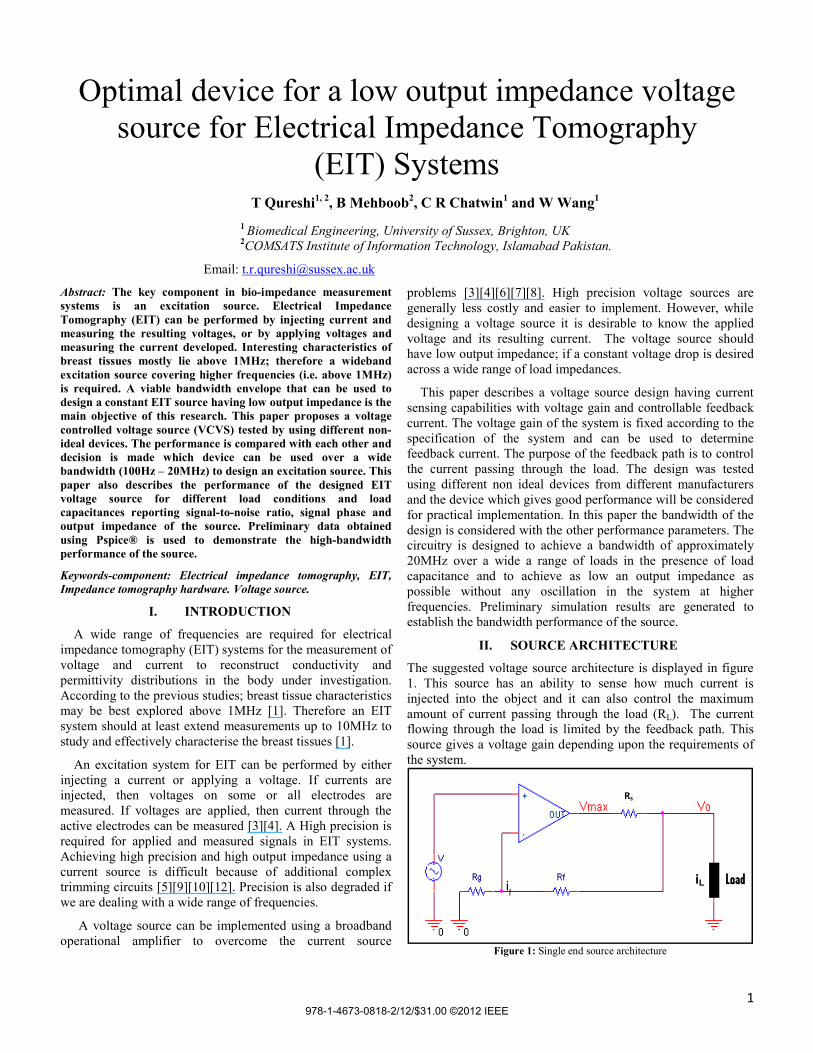
The suggested voltage source architecture is displayed in figure 1. This source has an ability to sense how much current is injected into the object and it can also control the maximum amount of current passing through the load (RL). The current flowing through the load is limited by the feedback path. This source gives a voltage gain depending upon the requirements of the system.
Figure 1: Single end source architecture
Rs
if iL
978-1-4673-0818-2/12/$31.00 ©2012 IEEE
2
The output current for the operational amplifier is given by:
1
The maximum operational amplifier output is given by: 2
Current passing through load depends upon the voltage gain of the system and can be expressed as: 3
III. METHODOLOGY
The circuit shown in figure 1 is simulated using Pspice® over a wide range of frequencies i.e. up to 1GHz. To facilitate high frequency capabilities; wide bandwidth components are chosen. System bandwidth limitations are mostly caused by amplifiers, therefore an amplifier with high gain bandwidth product must be chosen to ensure high frequency capability.
Three different devices are selected for the testing for the voltage source. These devices are OPA656, THS4304 and AD8055. OPA656 and THS4304 are from Texas instruments (TI) whilst AD8055 is from Analog devices (AD). OPA656 has a unity gain bandwidth product of 500MHz and can give 230 MHz gain bandwidth product with a gain of greater than 10. THS4304 has a unity gain bandwidth product of 3GHz and can give 870MHz gain bandwidth product with a gain of greater than 10. AD8055 has a unity gain bandwidth product of 300 MHz and can give 150 MHz gain bandwidth product with a gain of 2.
The minimum theoretical value of the load is decided and the circuit is tuned in such a manner that a constant voltage is dropped across the load with a maximum amount of current (i.e. 1mA) passing through the load. A differential amplifier is used across the sense resistor Rs to indirectly measure how much current is injected into the object. The op-amp output voltage varies with the change of the sense resistor Rs , as mentioned in equation 2. We need to specify certain parameters to find out the rest of the parameters in order to meet the design requirements. Firstly, the voltage gain of the system is set according to the specification. The theoretical maximum current (i.e. 1mA) will pass through the load when the load becomes equal to the voltage gain. For this case that value of the load can be considered as the minimum value of load attached to the source having a maximum current of 1mA. As mentioned earlier, the maximum operational amplifier voltage is dependent on Rs, so, in order to keep the maximum operational amplifier voltage in line with its data sheet range we have fixed its maximum value in equation 2 to find the optimum value of Rs which can be expressed as,
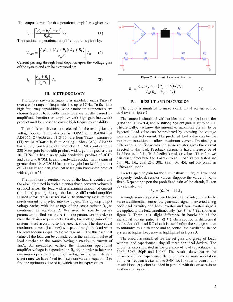
Figure 2: Differential source architecture 4
IV. RESULT AND DISCUSSION
The circuit is simulated to make a differential voltage source as shown in figure 2.
The source is simulated with an ideal and non-ideal amplifier (OPA656, THS4304, and AD8055). System gain is set to be 2.5. Theoretically, we know the amount of maximum current to be injected. Load value can be predicted by knowing the voltage gain and injected current. The predicted load value can be the minimum condition to allow maximum current. Practically, a differential amplifier across the sense resistor gives the current injected to the load. Feedback current is fixed irrespective of load because of the fixed feedback resistor values. Therefore we can easily determine the Load current. Load values tested are 5k, 10k, 15k, 20k, 25k, 30k, 35k, 40k, 45k and 50k ohms in differential mode.
To set a specific gain for the circuit shown in figure 1 we need to specify feedback resistor values. Suppose the value of Rg is fixed. Depending upon the predefined gain of the circuit, Rf can be calculated as: 1
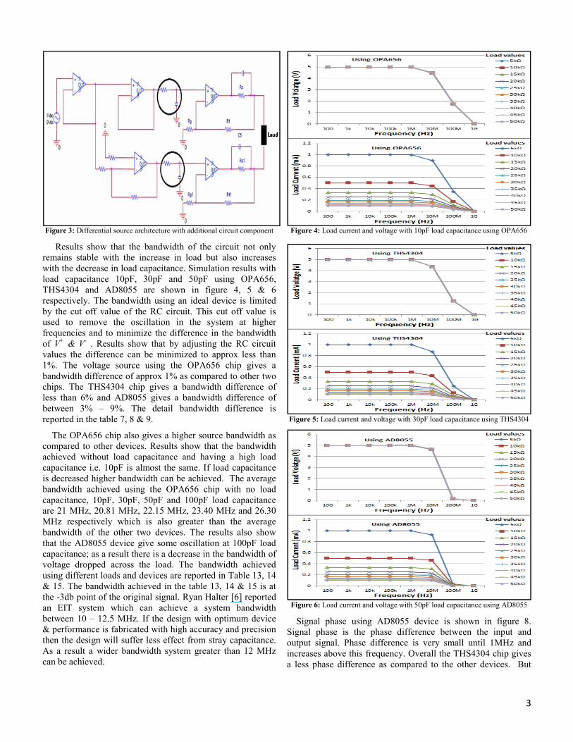
A single source signal is used to test the circuitry. In order to make a differential source, the generated signal is inverted using additional circuitry and both inverted and non-inverted signals are applied to the load simultaneously. (i.e. V+ & V-) as shown in figure 3. There is a slight difference in bandwidth of the individual voltage pulse (V+ & V-) when applied in differential mode. An additional RC circuit is used before the voltage source to minimize this difference and to control the oscillation in the system at higher frequency as highlighted in figure 3.
The circuit is simulated for the set gain and group of loads without load capacitance using all three non-ideal devices. The circuit is also simulated in the presence of load capacitance i.e. 10pF, 30pF, 50pF and 100pF. The results show that in the presence of load capacitance the circuit shows some oscillation at higher frequencies i.e. above 3-4MHz. In order to control this an additional capacitor is added in parallel with the sense resistor as shown in figure 3.
3
Figure 3: Differential source architecture with additional circuit component
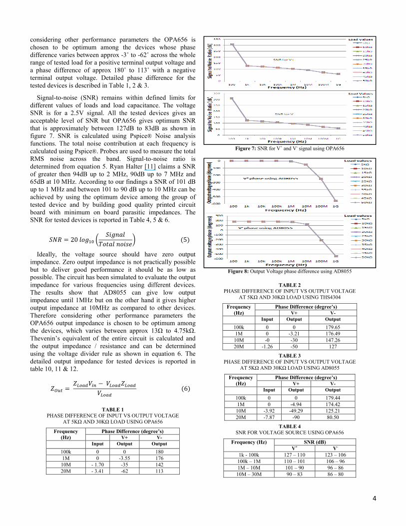
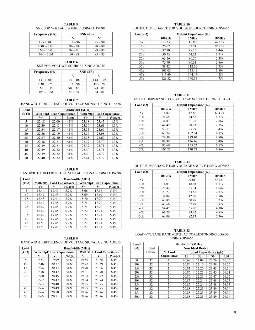
Results show that the bandwidth of the circuit not only remains stable with the increase in load but also increases with the decrease in load capacitance. Simulation results with load capacitance 10pF, 30pF and 50pF using OPA656, THS4304 and AD8055 are shown in figure 4, 5 & 6 respectively. The bandwidth using an ideal device is limited by the cut off value of the RC circuit. This cut off value is used to remove the oscillation in the system at higher frequencies and to minimize the difference in the bandwidth of V+ & V- . Results show that by adjusting the RC circuit values the difference can be minimized to approx less than 1%. The voltage source using the OPA656 chip gives a bandwidth difference of approx 1% as compared to other two chips. The THS4304 chip gives a bandwidth difference of less than 6% and AD8055 gives a bandwidth difference of between 3% – 9%. The detail bandwidth difference is reported in the table 7, 8 & 9.
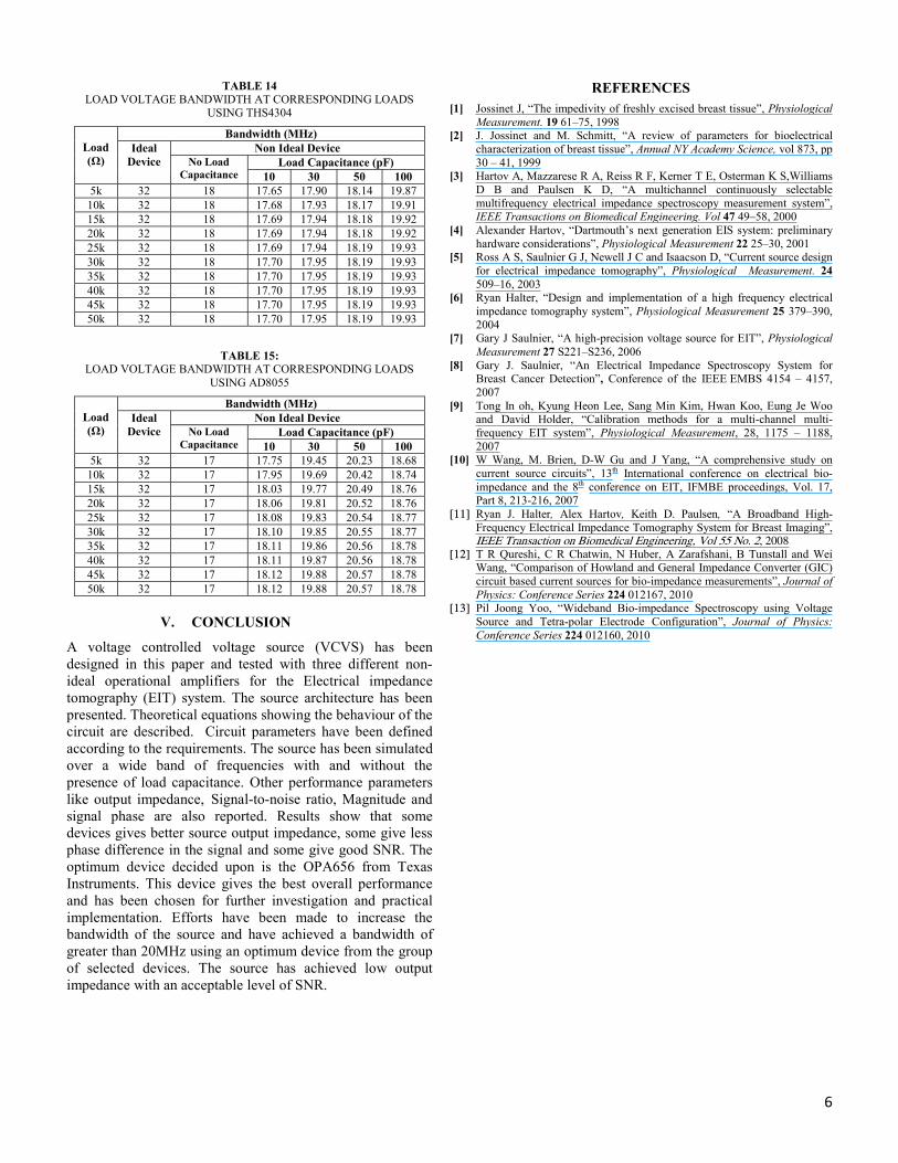
The OPA656 chip also gives a higher source bandwidth as compared to other devices. Results show that the bandwidth achieved without load capacitance and having a high load capacitance i.e. 10pF is almost the same. If load capacitance is decreased higher bandwidth can be achieved. The average bandwidth achieved using the OPA656 chip with no load capacitance, 10pF, 30pF, 50pF and 100pF load capacitance are 21 MHz, 20.81 MHz, 22.15 MHz, 23.40 MHz and 26.30 MHz respectively which is also greater than the average bandwidth of the other two devices. The results also show that the AD8055 device give some oscillation at 100pF load capacitance; as a result there is a decrease in the bandwidth of voltage dropped across the load. The bandwidth achieved using different loads and devices are reported in Table 13, 14 & 15. The bandwidth achieved in the table 13, 14 & 15 is at the -3db point of the original signal. Ryan Halter [6] reported an EIT system which can achieve a system bandwidth between 10 – 12.5 MHz. If the design with optimum device & performance is fabricated with high accuracy and precision then the design will suffer less effect from stray capacitance. As a result a wider bandwidth system greater than 12 MHz can be achieved.
Figure 4: Load current and voltage with 10pF load capacitance using OPA656
Figure 5: Load current and voltage with 30pF load capacitance using THS4304
Figure 6: Load current and voltage with 50pF load capacitance using AD8055
Signal phase using AD8055 device is shown in figure 8. Signal phase is the phase difference between the input and output signal. Phase difference is very small until 1MHz and increases above this frequency. Overall the THS4304 chip gives a less phase difference as compared to the other devices. But
4
considering other performance parameters the OPA656 is chosen to be optimum among the devices whose phase difference varies between approx -3˚ to -62˚ across the whole range of tested load for a positive terminal output voltage and a phase difference of approx 180˚ to 113˚ with a negative terminal output voltage. Detailed phase difference for the tested devices is described in Table 1, 2 & 3.
Signal-to-noise (SNR) remains within defined limits for different values of loads and load capacitance. The voltage SNR is for a 2.5V signal. All the tested devices gives an acceptable level of SNR but OPA656 gives optimum SNR that is approximately between 127dB to 83dB as shown in figure 7. SNR is calculated using Pspice® Noise analysis functions. The total noise contribution at each frequency is calculated using Pspice®. Probes are used to measure the total RMS noise across the band. Signal-to-noise ratio is determined from equation 5. Ryan Halter [11] claims a SNR of greater then 94dB up to 2 MHz, 90dB up to 7 MHz and 65dB at 10 MHz. According to our findings a SNR of 101 dB up to 1 MHz and between 101 to 90 dB up to 10 MHz can be achieved by using the optimum device among the group of tested device and by building good quality printed circuit board with minimum on board parasitic impedances. The SNR for tested devices is reported in Table 4, 5 & 6.
20 5
Ideally, the voltage source should have zero output impedance. Zero output impedance is not practically possible but to deliver good performance it should be as low as possible. The circuit has been simulated to evaluate the output impedance for various frequencies using different devices. The results show that AD8055 can give low output impedance until 1MHz but on the other hand it gives higher output impedance at 10MHz as compared to other devices. Therefore considering other performance parameters the OPA656 output impedance is chosen to be optimum among the devices, which varies between approx 13Ω to 4.75kΩ. Thevenin’s equivalent of the entire circuit is calculated and the output impedance / resistance and can be determined using the voltage divider rule as shown in equation 6. The detailed output impedance for tested devices is reported in table 10, 11 & 12.
6
TABLE 1
PHASE DIFFERENCE OF INPUT VS OUTPUT VOLTAGE AT 5KΩ AND 30KΩ LOAD USING OPA656
Frequency (Hz)
Phase Difference (degree’s) V+ V-
Input Output Output100k 0 0 180 1M 0 -3.55 176
10M - 1.70 -35 142 20M - 3.41 -62 113
Figure 7: SNR for V+ and V- signal using OPA656
Figure 8: Output Voltage phase difference using AD8055
TABLE 2
PHASE DIFFERENCE OF INPUT VS OUTPUT VOLTAGE AT 5KΩ AND 30KΩ LOAD USING THS4304
Frequency (Hz)
Phase Difference (degree’s) V+ V-
Input Output Output100k 0 0 179.65 1M 0 -3.21 176.49 10M -0 -30 147.26 20M -1.26 -50 127
TABLE 3 PHASE DIFFERENCE OF INPUT VS OUTPUT VOLTAGE
AT 5KΩ AND 30KΩ LOAD USING AD8055
Frequency (Hz)
Phase Difference (degree’s) V+ V-
Input Output Output100k 0 0 179.44 1M 0 -4.94 174.42 10M -3.92 -49.29 125.21 20M -7.87 -90 80.50
TABLE 4 SNR FOR VOLTAGE SOURCE USING OPA656
Frequency (Hz) SNR (dB) V+ V-
1k - 100k 127 – 110 123 – 106 100k – 1M 110 – 101 106 – 96 1M – 10M 101 – 90 96 – 86
10M – 30M 90 – 83 86 – 80
5
TABLE 5 SNR FOR VOLTAGE SOURCE USING THS4304
Frequency (Hz) SNR (dB) V+ V-
1k - 100k 101 – 96 95 – 90 100k – 1M 96 – 94 90 – 89 1M – 10M 94 – 90 89 – 85
10M – 30M 90 - 88 85 – 83
TABLE 6 SNR FOR VOLTAGE SOURCE USING AD8055
Frequency (Hz) SNR (dB) V+ V-
1k - 100k 117 – 107 114 – 103 100k – 1M 107 – 98 103 – 94 1M – 10M 98 – 88 94 – 84
10M – 30M 88 – 84 84 – 81
TABLE 7 BANDWIDTH DIFFERENCE OF VOLTAGE SIGNAL USING OPA656
Load (k Ω)
Bandwidth (MHz) With 30pF Load Capacitance With 50pF Load Capacitance
V+ V- (%age) V+ V- (%age)5 22.18 22.00 <1% 23.18 23.47 1.3%
10 22.30 22.13 <1% 23.30 23.61 1.3%15 22.34 22.17 <1% 23.35 23.66 1.3%20 22.36 22.19 <1% 23.37 23.68 1.3%25 22.37 22.20 <1% 23.38 23.69 1.3%30 22.38 22.21 <1% 23.39 23.70 1.3%35 22.39 22.21 <1% 23.39 23.71 1.3%40 22.39 22.22 <1% 23.40 23.71 1.3%45 22.39 22.22 <1% 23.40 23.72 1.3%50 22.40 22.22 <1% 23.41 23.72 1.3%
TABLE 8
BANDWIDTH DIFFERENCE OF VOLTAGE SIGNAL USING THS4304
Load (k Ω)
Bandwidth (MHz) With 30pF Load Capacitance With 50pF Load Capacitance
V+ V- (%age) V+ V- (%age)5 18.44 17.40 5.7% 18.66 17.66 5.4%
10 18.47 17.43 5.7% 18.69 17.69 5.4% 15 18.48 17.44 5.7% 18.70 17.70 5.4% 20 18.49 17.45 5.7% 18.71 17.70 5.4% 25 18.49 17.45 5.7% 18.71 17.70 5.4% 30 18.49 17.45 5.7% 18.72 17.71 5.4% 35 18.49 17.45 5.7% 18.72 17.71 5.4% 40 18.49 17.45 5.7% 18.72 17.71 5.4% 45 18.50 17.45 5.7% 18.72 17.71 5.4% 50 18.50 17.45 5.7% 18.72 17.71 5.4%
TABLE 9
BANDWIDTH DIFFERENCE OF VOLTAGE SIGNAL USING AD8055 Load (k Ω)
Bandwidth (MHz) With 30pF Load Capacitance With 50pF Load Capacitance
V+ V- (%age) V+ V- (%age)5 19.23 19.99 <4% 19.55 21.36 8.4%
10 19.46 20.27 <4% 19.72 21.59 8.4%15 19.54 20.37 <4% 19.78 21.66 8.4%20 19.58 20.42 <4% 19.81 21.70 8.4%25 19.60 20.45 <4% 19.83 21.72 8.4%30 19.62 20.47 <4% 19.84 21.74 8.4%35 19.63 20.48 <4% 19.85 21.75 8.4%40 19.64 20.49 <4% 19.85 21.75 8.4%45 19.64 20.50 <4% 19.86 21.76 8.4%50 19.65 20.51 <4% 19.86 21.76 8.4%
TABLE 10 OUTPUT IMPEDANCE FOR VOLTAGE SOURCE USING OPA656
Load (Ω) Output Impedance (Ω) 100kHz 1MHz 10MHz
5k 13.23 16.86 492.57 10k 25.67 32.51 965.39 15k 37.90 48.15 1.44k 20k 50.53 64.21 1.91k 25k 63.16 80.26 2.38k 30k 75.79 96.31 2.86k 35k 88.42 112.36 3.33k 40k 101.05 128.41 3.80k 45k 113.69 144.46 4.28k 50k 126.32 160.51 4.75k
TABLE 11 OUTPUT IMPEDANCE FOR VOLTAGE SOURCE USING THS4304
Load (Ω) Output Impedance (Ω) 100kHz 1MHz 10MHz
5k 11.02 17.66 694.24 10k 21.65 34.51 1.37k 15k 31.87 51.77 2.06k 20k 42.49 68.23 2.75k 25k 53.11 85.29 3.43k 30k 63.74 102.34 4.12k 35k 74.36 119.40 4.80k 40k 84.98 136.46 5.49k 45k 95.60 153.52 6.17k 50k 106.23 170.58 6.86k
TABLE 12 OUTPUT IMPEDANCE FOR VOLTAGE SOURCE USING AD8055
Load (Ω) Output Impedance (Ω) 100kHz 1MHz 10MHz
5k 7.21 9.81 581.60 10k 14.01 18.03 1.11k 15k 20.42 25.34 1.64k 20k 27.23 33.65 2.17k 25k 34.04 42.07 2.70k 30k 40.85 50.48 3.23k 35k 47.66 57.49 3.77k 40k 54.47 65.70 4.30k 45k 61.28 73.92 4.83k 50k 68.09 82.13 5.36k
TABLE 13 LOAD VOLTAGE BANDWIDTH AT CORRESPONDING LOADS
USING OPA656
Load (Ω)
Bandwidth (MHz) Ideal
Device Non Ideal Device
No Load Capacitance
Load Capacitance (pF) 10 30 50 100
5k 32 21 20.69 22.04 23.26 26.16 10k 32 21 20.80 22.16 23.39 26.26 15k 32 21 20.83 22.20 23.43 26.30 20k 32 21 20.85 22.22 23.45 26.31 25k 32 21 20.86 22.23 23.47 26.32 30k 32 21 20.87 22.24 23.48 26.33 35k 32 21 20.87 22.24 23.48 26.33 40k 32 21 20.88 22.25 23.49 26.34 45k 32 21 20.88 22.25 23.49 26.34 50k 32 21 20.88 22.25 23.49 26.34
6
TABLE 14 LOAD VOLTAGE BANDWIDTH AT CORRESPONDING LOADS
USING THS4304
Load (Ω)
Bandwidth (MHz) Ideal
Device Non Ideal Device
No Load Capacitance
Load Capacitance (pF) 10 30 50 100
5k 32 18 17.65 17.90 18.14 19.87 10k 32 18 17.68 17.93 18.17 19.9115k 32 18 17.69 17.94 18.18 19.9220k 32 18 17.69 17.94 18.18 19.9225k 32 18 17.69 17.94 18.19 19.9330k 32 18 17.70 17.95 18.19 19.9335k 32 18 17.70 17.95 18.19 19.9340k 32 18 17.70 17.95 18.19 19.9345k 32 18 17.70 17.95 18.19 19.9350k 32 18 17.70 17.95 18.19 19.93
TABLE 15:
LOAD VOLTAGE BANDWIDTH AT CORRESPONDING LOADS USING AD8055
Load (Ω)
Bandwidth (MHz) Ideal
Device Non Ideal Device
No Load Capacitance
Load Capacitance (pF) 10 30 50 100
5k 32 17 17.75 19.45 20.23 18.68 10k 32 17 17.95 19.69 20.42 18.7415k 32 17 18.03 19.77 20.49 18.7620k 32 17 18.06 19.81 20.52 18.7625k 32 17 18.08 19.83 20.54 18.7730k 32 17 18.10 19.85 20.55 18.7735k 32 17 18.11 19.86 20.56 18.7840k 32 17 18.11 19.87 20.56 18.7845k 32 17 18.12 19.88 20.57 18.7850k 32 17 18.12 19.88 20.57 18.78
V. CONCLUSION
A voltage controlled voltage source (VCVS) has been designed in this paper and tested with three different non-ideal operational amplifiers for the Electrical impedance tomography (EIT) system. The source architecture has been presented. Theoretical equations showing the behaviour of the circuit are described. Circuit parameters have been defined according to the requirements. The source has been simulated over a wide band of frequencies with and without the presence of load capacitance. Other performance parameters like output impedance, Signal-to-noise ratio, Magnitude and signal phase are also reported. Results show that some devices gives better source output impedance, some give less phase difference in the signal and some give good SNR. The optimum device decided upon is the OPA656 from Texas Instruments. This device gives the best overall performance and has been chosen for further investigation and practical implementation. Efforts have been made to increase the bandwidth of the source and have achieved a bandwidth of greater than 20MHz using an optimum device from the group of selected devices. The source has achieved low output impedance with an acceptable level of SNR.
REFERENCES [1] Jossinet J, “The impedivity of freshly excised breast tissue”, Physiological
Measurement. 19 61–75, 1998 [2] J. Jossinet and M. Schmitt, “A review of parameters for bioelectrical
characterization of breast tissue”, Annual NY Academy Science, vol 873, pp 30 – 41, 1999
[3] Hartov A, Mazzarese R A, Reiss R F, Kerner T E, Osterman K S,Williams D B and Paulsen K D, “A multichannel continuously selectable multifrequency electrical impedance spectroscopy measurement system”, IEEE Transactions on Biomedical Engineering. Vol 47 49–58, 2000
[4] Alexander Hartov, “Dartmouth’s next generation EIS system: preliminary hardware considerations”, Physiological Measurement 22 25–30, 2001
[5] Ross A S, Saulnier G J, Newell J C and Isaacson D, “Current source design for electrical impedance tomography”, Physiological Measurement. 24 509–16, 2003
[6] Ryan Halter, “Design and implementation of a high frequency electrical impedance tomography system”, Physiological Measurement 25 379–390, 2004
[7] Gary J Saulnier, “A high-precision voltage source for EIT”, Physiological Measurement 27 S221–S236, 2006
[8] Gary J. Saulnier, “An Electrical Impedance Spectroscopy System for Breast Cancer Detection”, Conference of the IEEE EMBS 4154 – 4157, 2007
[9] Tong In oh, Kyung Heon Lee, Sang Min Kim, Hwan Koo, Eung Je Woo and David Holder, “Calibration methods for a multi-channel multi-frequency EIT system”, Physiological Measurement, 28, 1175 – 1188, 2007
[10] W Wang, M. Brien, D-W Gu and J Yang, “A comprehensive study on current source circuits”, 13th International conference on electrical bio-impedance and the 8th conference on EIT, IFMBE proceedings, Vol. 17, Part 8, 213-216, 2007
[11] Ryan J. Halter, Alex Hartov, Keith D. Paulsen, “A Broadband High-Frequency Electrical Impedance Tomography System for Breast Imaging”, IEEE Transaction on Biomedical Engineering, Vol 55 No. 2, 2008
[12] T R Qureshi, C R Chatwin, N Huber, A Zarafshani, B Tunstall and Wei Wang, “Comparison of Howland and General Impedance Converter (GIC) circuit based current sources for bio-impedance measurements”, Journal of Physics: Conference Series 224 012167, 2010
[13] Pil Joong Yoo, “Wideband Bio-impedance Spectroscopy using Voltage Source and Tetra-polar Electrode Configuration”, Journal of Physics: Conference Series 224 012160, 2010