open-q™ 820 μsom hw device specification
TRANSCRIPT
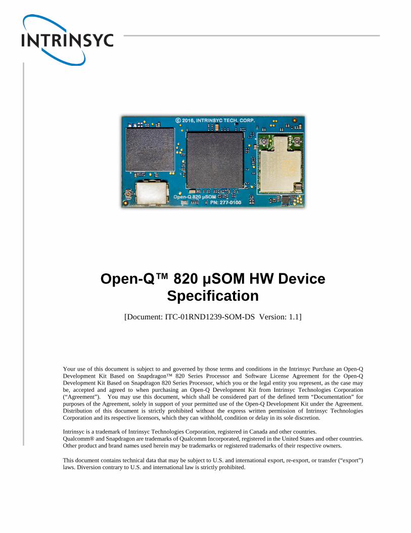
Open-Q™ 820 μSOM HW Device Specification
[Document: ITC-01RND1239-SOM-DS Version: 1.1]
Your use of this document is subject to and governed by those terms and conditions in the Intrinsyc Purchase an Open-Q Development Kit Based on Snapdragon™ 820 Series Processor and Software License Agreement for the Open-Q Development Kit Based on Snapdragon 820 Series Processor, which you or the legal entity you represent, as the case may be, accepted and agreed to when purchasing an Open-Q Development Kit from Intrinsyc Technologies Corporation (“Agreement”). You may use this document, which shall be considered part of the defined term “Documentation” for purposes of the Agreement, solely in support of your permitted use of the Open-Q Development Kit under the Agreement. Distribution of this document is strictly prohibited without the express written permission of Intrinsyc Technologies Corporation and its respective licensors, which they can withhold, condition or delay in its sole discretion. Intrinsyc is a trademark of Intrinsyc Technologies Corporation, registered in Canada and other countries. Qualcomm® and Snapdragon are trademarks of Qualcomm Incorporated, registered in the United States and other countries. Other product and brand names used herein may be trademarks or registered trademarks of their respective owners. This document contains technical data that may be subject to U.S. and international export, re-export, or transfer (“export”) laws. Diversion contrary to U.S. and international law is strictly prohibited.
Open-Q™ 820 μSOM HW Device Specification v. 1.1
1 Copyright Intrinsyc Technologies Corporation
Identification Document Title Open-Q™ 820 μSOM HW Device Specification
Document Number ITC-01RND1239-SOM-DS
Version 1.1
Date May 16, 2019
History
REVISION DATE DESCRIPTION PAGES
1.0 Jan 18, 2018 Initial Draft All
1.1 May 16, 2019 Updated outline to new standard All
Open-Q™ 820 μSOM HW Device Specification v. 1.1
2 Copyright Intrinsyc Technologies Corporation
Table of Contents 1. INTRODUCTION .................................................................................. 4
1.1 Purpose ........................................................................................................ 4 1.2 Scope ........................................................................................................... 4 1.3 Intended Audience ...................................................................................... 4 1.4 Acronyms and Abbreviations ..................................................................... 4 1.5 Signal Name Suffix ..................................................................................... 5
2. DOCUMENTS ....................................................................................... 6
2.1 Applicable Documents ................................................................................ 6 2.2 Reference Documents ................................................................................. 6
3. SUMMARY OF FEATURES ................................................................. 7
3.1 µSOM BLOCK DIAGRAM ....................................................................... 7 3.2 µSOM Technical Specifications ................................................................. 8
4. I/O DEFINITIONS ................................................................................. 9
4.1 Location of Major Components .................................................................. 9 4.2 B2B Connector Signal Assignments ......................................................... 11
5. ELECTRICAL SPECIFICATIONS ...................................................... 19
5.1 Absolute Maximum Ratings ..................................................................... 19 5.2 Operating Conditions ................................................................................ 19 5.3 Operating Temperature ............................................................................. 19 5.4 Power Consumption .................................................................................. 20
5.4.1 Setup and Methodology ........................................................................................... 20 5.4.2 Results ..................................................................................................................... 21
5.5 ESD Ratings .............................................................................................. 21
6. MECHANICAL SPECIFICATIONS ..................................................... 22
6.1 µSOM Mechanical Outline ....................................................................... 22 6.2 Top and Bottom Height Restrictions ........................................................ 22 6.3 Landing Pattern ......................................................................................... 22 6.4 Thermal Characteristics ............................................................................ 23 6.5 Weight ....................................................................................................... 23 6.6 B2B Connector use Limit ......................................................................... 23
7. PRODUCT MARKING, ORDERING, AND STORAGE INFO ............. 24
7.1 Product Marking ....................................................................................... 24 7.2 Product Ordering Information ................................................................... 24 7.3 Packaging and Shipping Information ........................................................ 24
8. HANDLING PRECAUTIONS .............................................................. 26
8.1 ESD Precautions ....................................................................................... 26 8.2 SOM – Carrier Board Mating Cautions .................................................... 26 8.3 Storage ...................................................................................................... 26
Open-Q™ 820 μSOM HW Device Specification v. 1.1
3 Copyright Intrinsyc Technologies Corporation
9. CERTIFICATION ................................................................................ 27
9.1 Radio Certification .................................................................................... 27 9.2 ROHS/REACH Compliance ..................................................................... 27
10. COMPANY CONTACT ....................................................................... 28
Open-Q™ 820 μSOM HW Device Specification v. 1.1
4 Copyright Intrinsyc Technologies Corporation
1. INTRODUCTION This document applies to the Open-Q 820 μSOM only. The Intrinsyc product line also includes the Open-Q 820 SOM and technical specification of that module is covered under a separate document.
1.1 Purpose The purpose of this document is to provide a technical overview of the Intrinsyc Open-Q 820 μSOM. For more information on the associated Open-Q 820 μSOM Development Kit and accessories, see the website here:
https://www.intrinsyc.com/snapdragon-embedded-development-kits/open-q-820-usom-development-kit/
1.2 Scope This document covers the following information on the Open-Q 820 μSOM:
• Electrical and mechanical specifications • µSOM pin-out • Device handling and packaging • Ordering information.
1.3 Intended Audience This document is intended for users who wish to understand the technical specifications of the Intrinsyc Open-Q 820 μSOM.
1.4 Acronyms and Abbreviations Acronym / Abbreviation
Definition
ANT ANTenna BAT, BATT BATTery BAM Bus Access Manager BLSP BAM-based Low-Speed Peripheral BOM Bill Of Materials BT Blue Tooth CLK Clock CPU Central Processing Unit CS Chip Select CSI Camera Serial Interface DSI Display Serial Interface EMI Electro-Magnetic Interference EN ENable ERM Eccentric Rotating Mass ESD Electro-Static Discharge GND GrouND GPIO General Purpose I/O GPS Global Positioning System
Open-Q™ 820 μSOM HW Device Specification v. 1.1
5 Copyright Intrinsyc Technologies Corporation
Acronym / Abbreviation
Definition
HDMI High Definition Multimedia Interface I2C Inter-Integrated Circuit I2S Inter-IC Sound INT INTerrupt JTAG Joint Test Action Group LDO Low Drop-Out LRM Linear Resonant Actuator LTE Long-Term Evolution MDP Mobile Display Port MI2S Mobile Inter-IC Sound MIC MICrophone MIPI Mobile Industry Processor Interface MPP Multi-Purpose Pin NFC Near Field Communication PCB Printed Circuit Board PCIE Peripheral Component Interconnect Express PWM Pulse-Width Modulation RF Radio Frequency RX Receive SCL Serial CLock SDA Serial DAta SDC Secure Digital Interface SOM System On Module SPI Serial Peripheral Interface SSC Snapdragon Sensor Core TX Transmit UART Universal Asynchronous Receiver/Transmiter UIM User Interface Module USB Universal Serial Bus WLAN Wireless Local Area Network
1.5 Signal Name Suffix Suffix Definition _N Indicates that the signal is ACTIVE LOW _P/N Identifies the two signals comprising a differential pair
Open-Q™ 820 μSOM HW Device Specification v. 1.1
6 Copyright Intrinsyc Technologies Corporation
2. DOCUMENTS This section lists any parent and supplementary documents for the Open-Q 820 μSOM Device Specification. Unless stated otherwise, applicable documents supersede this document and reference documents provide background and supplementary information.
2.1 Applicable Documents
REFERENCE AUTHOR TITLE
A-1 Intrinsyc Intrinsyc Purchase and Software License Agreement for the Open-Q 820 μSOM
2.2 Reference Documents
REFERENCE TITLE
R-1 Hardware Document Set for the Snapdragon APQ8096 based Open-Q Development Kit: https://support.intrinsyc.com/documents/253
R-2 Intrinsyc Open-Q 820 (APQ8096) µSOM Development Kit: Technical Note 19: µSOM Carrier Board Design Guide: https://support.intrinsyc.com/documents/214
R-3 Open-Q 820 µSOM Schematics (µSOM): https://support.intrinsyc.com/documents/199
R-4 Intrinsyc Open-Q 820 µSOM Development Kit User Guide: https://support.intrinsyc.com/documents/212
R-5 ITCNFA324 Module Certification OEM Integrator Instructions: https://support.intrinsyc.com/documents/224
Open-Q™ 820 μSOM HW Device Specification v. 1.1
7 Copyright Intrinsyc Technologies Corporation
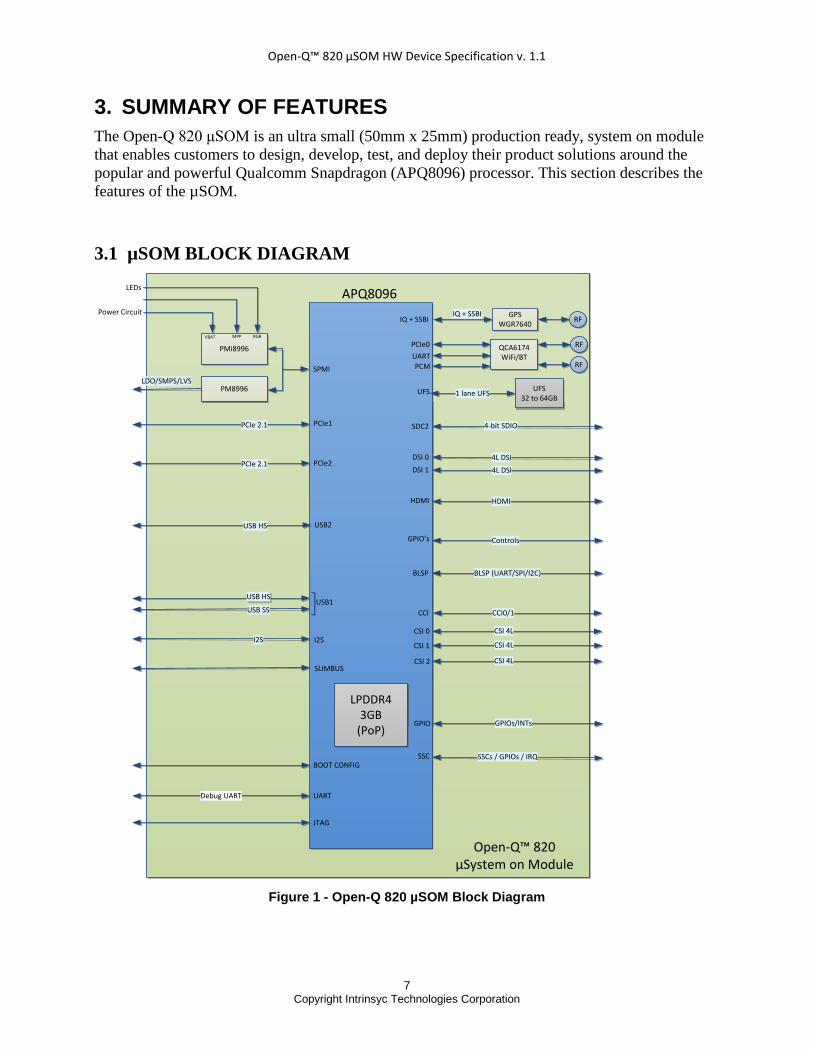
3. SUMMARY OF FEATURES The Open-Q 820 μSOM is an ultra small (50mm x 25mm) production ready, system on module that enables customers to design, develop, test, and deploy their product solutions around the popular and powerful Qualcomm Snapdragon (APQ8096) processor. This section describes the features of the µSOM.
3.1 µSOM BLOCK DIAGRAM
`
APQ8096
LPDDR43GB
(PoP)
PMi8996
PM8996
4-bit SDIO
4L DSI
BLSP (UART/SPI/I2C)
USB HS
USB SS
HDMI
QCA6174WiFi/BT
GPSWGR7640
Open-Q™ 820µSystem on Module
SLIMBUS
IQ + SSBI
4L DSI
CSI 0
CSI 1
CSI 2
USB HS USB2
SSCs / GPIOs / IRQ
DSI 0
DSI 1
Controls
USB1
I2S
PCIe0
GPIO’s
CCI0/1
UFS32 to 64GB
UFS 1 lane UFS
PCMUART
SPMI
SDC2
HDMI
JTAG
Debug UART UART
PCIe1
PCIe2
PCIe 2.1
PCIe 2.1
I2SCSI 4L
CSI 4L
CSI 4L
GPIOs/INTs
BOOT CONFIG
RF
RF
RF
Power Circuit
LEDs
RGBMPPVBAT
IQ + SSBI
BLSP
CCI
SSC
GPIO
LDO/SMPS/LVS
Figure 1 - Open-Q 820 µSOM Block Diagram
Open-Q™ 820 μSOM HW Device Specification v. 1.1
8 Copyright Intrinsyc Technologies Corporation
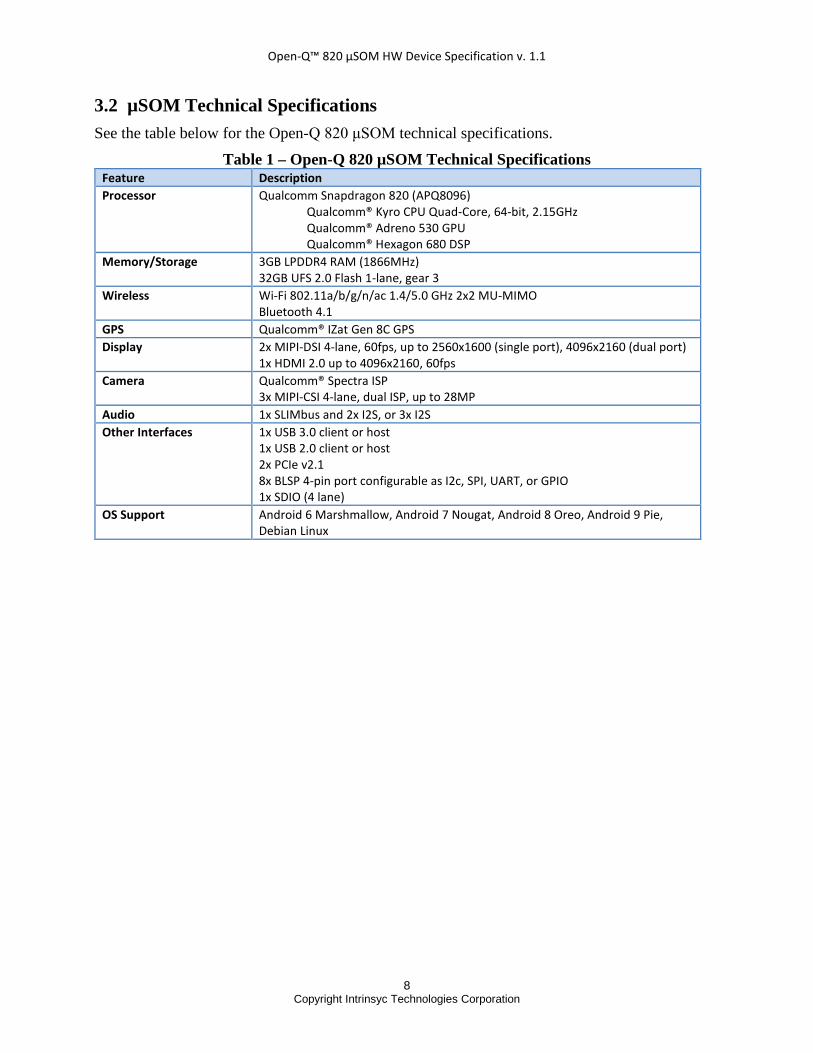
3.2 µSOM Technical Specifications See the table below for the Open-Q 820 μSOM technical specifications.
Table 1 – Open-Q 820 µSOM Technical Specifications Feature Description Processor Qualcomm Snapdragon 820 (APQ8096)
Qualcomm® Kyro CPU Quad-Core, 64-bit, 2.15GHz Qualcomm® Adreno 530 GPU Qualcomm® Hexagon 680 DSP
Memory/Storage 3GB LPDDR4 RAM (1866MHz) 32GB UFS 2.0 Flash 1-lane, gear 3
Wireless Wi-Fi 802.11a/b/g/n/ac 1.4/5.0 GHz 2x2 MU-MIMO Bluetooth 4.1
GPS Qualcomm® IZat Gen 8C GPS Display 2x MIPI-DSI 4-lane, 60fps, up to 2560x1600 (single port), 4096x2160 (dual port)
1x HDMI 2.0 up to 4096x2160, 60fps Camera Qualcomm® Spectra ISP
3x MIPI-CSI 4-lane, dual ISP, up to 28MP Audio 1x SLIMbus and 2x I2S, or 3x I2S Other Interfaces 1x USB 3.0 client or host
1x USB 2.0 client or host 2x PCIe v2.1 8x BLSP 4-pin port configurable as I2c, SPI, UART, or GPIO 1x SDIO (4 lane)
OS Support Android 6 Marshmallow, Android 7 Nougat, Android 8 Oreo, Android 9 Pie, Debian Linux
Open-Q™ 820 μSOM HW Device Specification v. 1.1
9 Copyright Intrinsyc Technologies Corporation
4. I/O DEFINITIONS
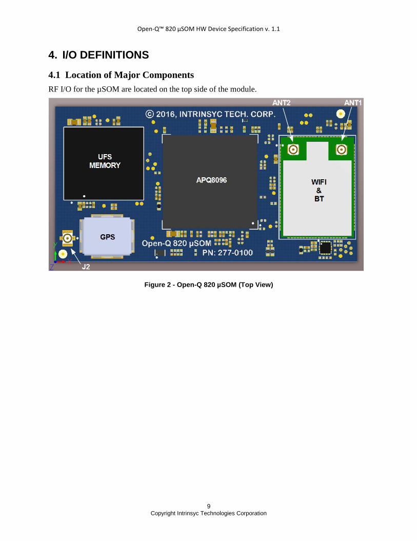
4.1 Location of Major Components RF I/O for the µSOM are located on the top side of the module.
Figure 2 - Open-Q 820 µSOM (Top View)
Open-Q™ 820 μSOM HW Device Specification v. 1.1
10 Copyright Intrinsyc Technologies Corporation
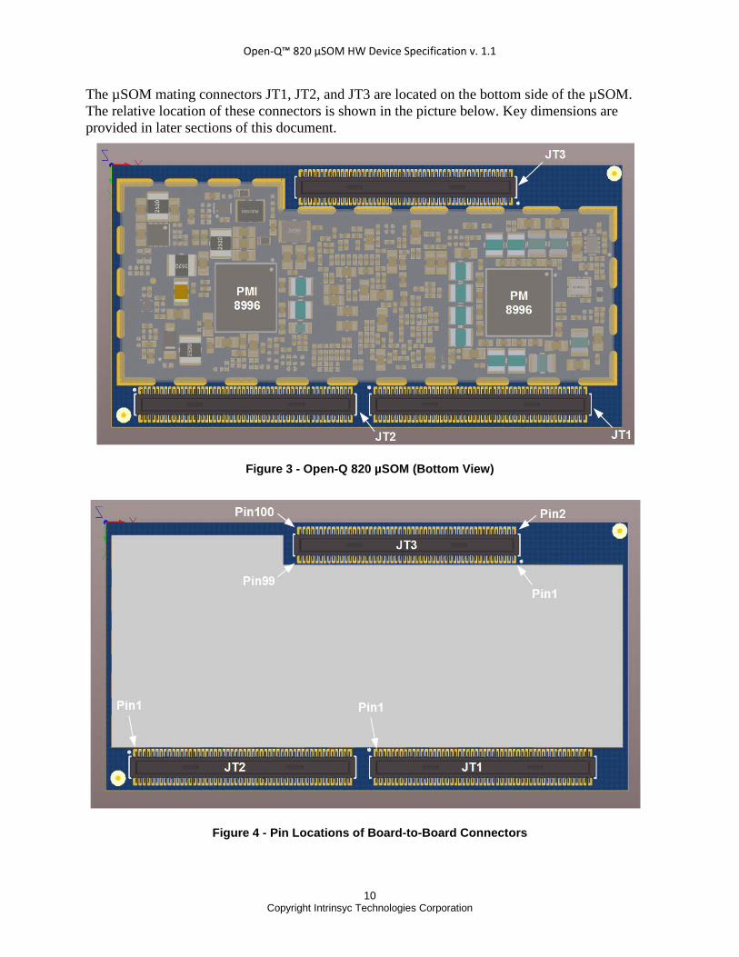
The µSOM mating connectors JT1, JT2, and JT3 are located on the bottom side of the µSOM. The relative location of these connectors is shown in the picture below. Key dimensions are provided in later sections of this document.
Figure 3 - Open-Q 820 µSOM (Bottom View)
Figure 4 - Pin Locations of Board-to-Board Connectors
Open-Q™ 820 μSOM HW Device Specification v. 1.1
11 Copyright Intrinsyc Technologies Corporation
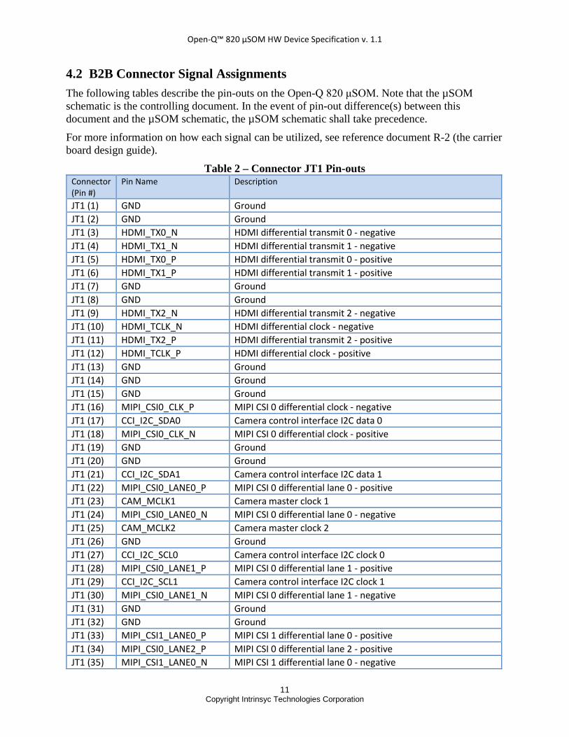
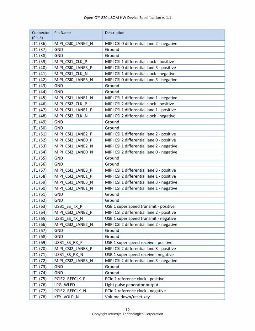
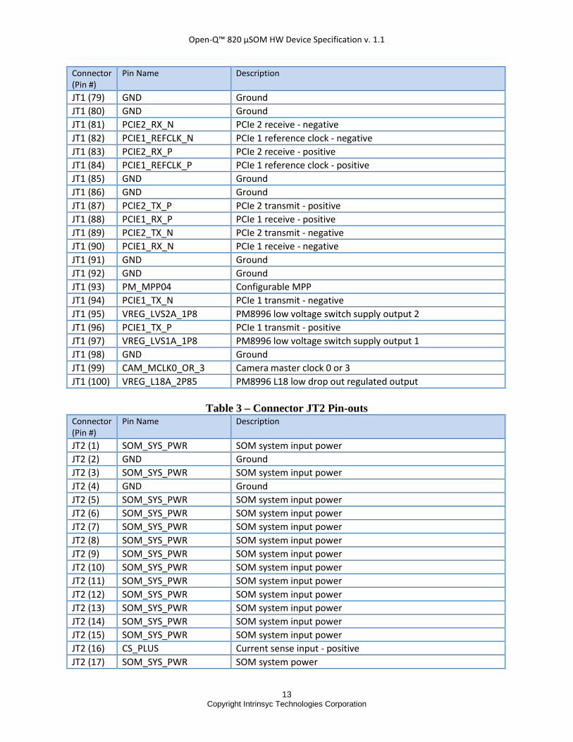
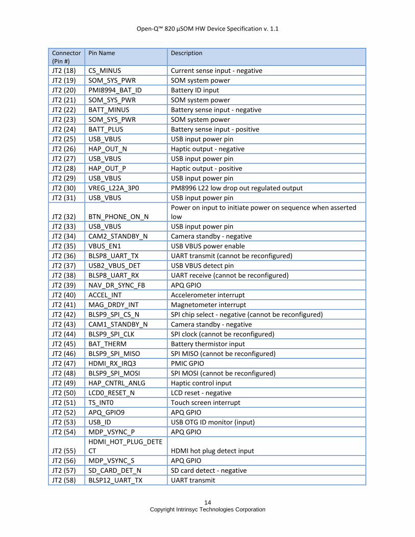
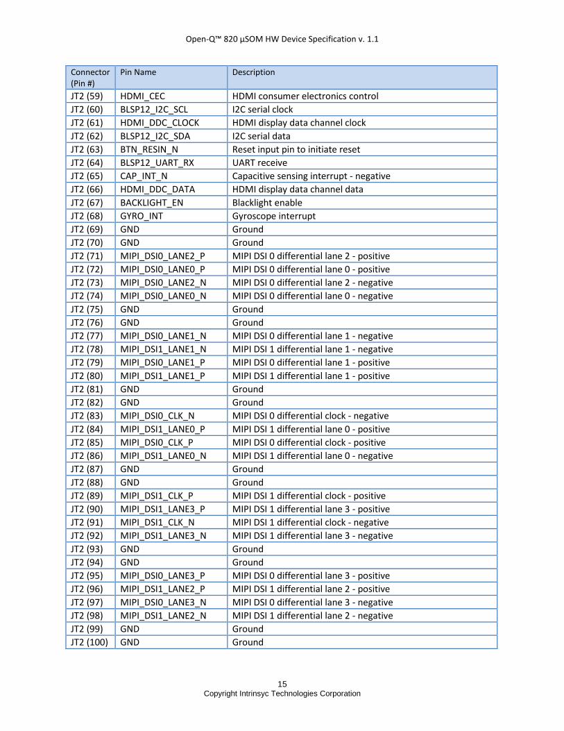
4.2 B2B Connector Signal Assignments The following tables describe the pin-outs on the Open-Q 820 μSOM. Note that the µSOM schematic is the controlling document. In the event of pin-out difference(s) between this document and the µSOM schematic, the µSOM schematic shall take precedence.
For more information on how each signal can be utilized, see reference document R-2 (the carrier board design guide).
Table 2 – Connector JT1 Pin-outs Connector (Pin #)
Pin Name Description
JT1 (1) GND Ground JT1 (2) GND Ground JT1 (3) HDMI_TX0_N HDMI differential transmit 0 - negative JT1 (4) HDMI_TX1_N HDMI differential transmit 1 - negative JT1 (5) HDMI_TX0_P HDMI differential transmit 0 - positive JT1 (6) HDMI_TX1_P HDMI differential transmit 1 - positive JT1 (7) GND Ground JT1 (8) GND Ground JT1 (9) HDMI_TX2_N HDMI differential transmit 2 - negative JT1 (10) HDMI_TCLK_N HDMI differential clock - negative JT1 (11) HDMI_TX2_P HDMI differential transmit 2 - positive JT1 (12) HDMI_TCLK_P HDMI differential clock - positive JT1 (13) GND Ground JT1 (14) GND Ground JT1 (15) GND Ground JT1 (16) MIPI_CSI0_CLK_P MIPI CSI 0 differential clock - negative JT1 (17) CCI_I2C_SDA0 Camera control interface I2C data 0 JT1 (18) MIPI_CSI0_CLK_N MIPI CSI 0 differential clock - positive JT1 (19) GND Ground JT1 (20) GND Ground JT1 (21) CCI_I2C_SDA1 Camera control interface I2C data 1 JT1 (22) MIPI_CSI0_LANE0_P MIPI CSI 0 differential lane 0 - positive JT1 (23) CAM_MCLK1 Camera master clock 1 JT1 (24) MIPI_CSI0_LANE0_N MIPI CSI 0 differential lane 0 - negative JT1 (25) CAM_MCLK2 Camera master clock 2 JT1 (26) GND Ground JT1 (27) CCI_I2C_SCL0 Camera control interface I2C clock 0 JT1 (28) MIPI_CSI0_LANE1_P MIPI CSI 0 differential lane 1 - positive JT1 (29) CCI_I2C_SCL1 Camera control interface I2C clock 1 JT1 (30) MIPI_CSI0_LANE1_N MIPI CSI 0 differential lane 1 - negative JT1 (31) GND Ground JT1 (32) GND Ground JT1 (33) MIPI_CSI1_LANE0_P MIPI CSI 1 differential lane 0 - positive JT1 (34) MIPI_CSI0_LANE2_P MIPI CSI 0 differential lane 2 - positive JT1 (35) MIPI_CSI1_LANE0_N MIPI CSI 1 differential lane 0 - negative
Open-Q™ 820 μSOM HW Device Specification v. 1.1
12 Copyright Intrinsyc Technologies Corporation
Connector (Pin #)
Pin Name Description
JT1 (36) MIPI_CSI0_LANE2_N MIPI CSI 0 differential lane 2 - negative JT1 (37) GND Ground JT1 (38) GND Ground JT1 (39) MIPI_CSI1_CLK_P MIPI CSI 1 differential clock - positive JT1 (40) MIPI_CSI0_LANE3_P MIPI CSI 0 differential lane 3 - positive JT1 (41) MIPI_CSI1_CLK_N MIPI CSI 1 differential clock - negative JT1 (42) MIPI_CSI0_LANE3_N MIPI CSI 0 differential lane 3 - negative JT1 (43) GND Ground JT1 (44) GND Ground JT1 (45) MIPI_CSI1_LANE1_N MIPI CSI 1 differential lane 1 - negative JT1 (46) MIPI_CSI2_CLK_P MIPI CSI 2 differential clock - positive JT1 (47) MIPI_CSI1_LANE1_P MIPI CSI 1 differential lane 1 - positive JT1 (48) MIPI_CSI2_CLK_N MIPI CSI 2 differential clock - negative JT1 (49) GND Ground JT1 (50) GND Ground JT1 (51) MIPI_CSI1_LANE2_P MIPI CSI 1 differential lane 2 - positive JT1 (52) MIPI_CSI2_LANE0_P MIPI CSI 2 differential lane 0 - positive JT1 (53) MIPI_CSI1_LANE2_N MIPI CSI 1 differential lane 2 - negative JT1 (54) MIPI_CSI2_LANE0_N MIPI CSI 2 differential lane 0 - negative JT1 (55) GND Ground JT1 (56) GND Ground JT1 (57) MIPI_CSI1_LANE3_P MIPI CSI 1 differential lane 3 - positive JT1 (58) MIPI_CSI2_LANE1_P MIPI CSI 2 differential lane 1 - positive JT1 (59) MIPI_CSI1_LANE3_N MIPI CSI 1 differential lane 3 - negative JT1 (60) MIPI_CSI2_LANE1_N MIPI CSI 2 differential lane 1 - negative JT1 (61) GND Ground JT1 (62) GND Ground JT1 (63) USB1_SS_TX_P USB 1 super speed transmit - positive JT1 (64) MIPI_CSI2_LANE2_P MIPI CSI 2 differential lane 2 - positive JT1 (65) USB1_SS_TX_N USB 1 super speed transmit - negative JT1 (66) MIPI_CSI2_LANE2_N MIPI CSI 2 differential lane 2 - negative JT1 (67) GND Ground JT1 (68) GND Ground JT1 (69) USB1_SS_RX_P USB 1 super speed receive - positive JT1 (70) MIPI_CSI2_LANE3_P MIPI CSI 2 differential lane 3 - positive JT1 (71) USB1_SS_RX_N USB 1 super speed receive - negative JT1 (72) MIPI_CSI2_LANE3_N MIPI CSI 2 differential lane 3 - negative JT1 (73) GND Ground JT1 (74) GND Ground JT1 (75) PCIE2_REFCLK_P PCIe 2 reference clock - positive JT1 (76) LPG_WLED Light pulse generator output JT1 (77) PCIE2_REFCLK_N PCIe 2 reference clock - negative JT1 (78) KEY_VOLP_N Volume down/reset key
Open-Q™ 820 μSOM HW Device Specification v. 1.1
13 Copyright Intrinsyc Technologies Corporation
Connector (Pin #)
Pin Name Description
JT1 (79) GND Ground JT1 (80) GND Ground JT1 (81) PCIE2_RX_N PCIe 2 receive - negative JT1 (82) PCIE1_REFCLK_N PCIe 1 reference clock - negative JT1 (83) PCIE2_RX_P PCIe 2 receive - positive JT1 (84) PCIE1_REFCLK_P PCIe 1 reference clock - positive JT1 (85) GND Ground JT1 (86) GND Ground JT1 (87) PCIE2_TX_P PCIe 2 transmit - positive JT1 (88) PCIE1_RX_P PCIe 1 receive - positive JT1 (89) PCIE2_TX_N PCIe 2 transmit - negative JT1 (90) PCIE1_RX_N PCIe 1 receive - negative JT1 (91) GND Ground JT1 (92) GND Ground JT1 (93) PM_MPP04 Configurable MPP JT1 (94) PCIE1_TX_N PCIe 1 transmit - negative JT1 (95) VREG_LVS2A_1P8 PM8996 low voltage switch supply output 2 JT1 (96) PCIE1_TX_P PCIe 1 transmit - positive JT1 (97) VREG_LVS1A_1P8 PM8996 low voltage switch supply output 1 JT1 (98) GND Ground JT1 (99) CAM_MCLK0_OR_3 Camera master clock 0 or 3 JT1 (100) VREG_L18A_2P85 PM8996 L18 low drop out regulated output
Table 3 – Connector JT2 Pin-outs
Connector (Pin #)
Pin Name Description
JT2 (1) SOM_SYS_PWR SOM system input power JT2 (2) GND Ground JT2 (3) SOM_SYS_PWR SOM system input power JT2 (4) GND Ground JT2 (5) SOM_SYS_PWR SOM system input power JT2 (6) SOM_SYS_PWR SOM system input power JT2 (7) SOM_SYS_PWR SOM system input power JT2 (8) SOM_SYS_PWR SOM system input power JT2 (9) SOM_SYS_PWR SOM system input power JT2 (10) SOM_SYS_PWR SOM system input power JT2 (11) SOM_SYS_PWR SOM system input power JT2 (12) SOM_SYS_PWR SOM system input power JT2 (13) SOM_SYS_PWR SOM system input power JT2 (14) SOM_SYS_PWR SOM system input power JT2 (15) SOM_SYS_PWR SOM system input power JT2 (16) CS_PLUS Current sense input - positive JT2 (17) SOM_SYS_PWR SOM system power
Open-Q™ 820 μSOM HW Device Specification v. 1.1
14 Copyright Intrinsyc Technologies Corporation
Connector (Pin #)
Pin Name Description
JT2 (18) CS_MINUS Current sense input - negative JT2 (19) SOM_SYS_PWR SOM system power JT2 (20) PMI8994_BAT_ID Battery ID input JT2 (21) SOM_SYS_PWR SOM system power JT2 (22) BATT_MINUS Battery sense input - negative JT2 (23) SOM_SYS_PWR SOM system power JT2 (24) BATT_PLUS Battery sense input - positive JT2 (25) USB_VBUS USB input power pin JT2 (26) HAP_OUT_N Haptic output - negative JT2 (27) USB_VBUS USB input power pin JT2 (28) HAP_OUT_P Haptic output - positive JT2 (29) USB_VBUS USB input power pin JT2 (30) VREG_L22A_3P0 PM8996 L22 low drop out regulated output JT2 (31) USB_VBUS USB input power pin
JT2 (32) BTN_PHONE_ON_N Power on input to initiate power on sequence when asserted low
JT2 (33) USB_VBUS USB input power pin JT2 (34) CAM2_STANDBY_N Camera standby - negative JT2 (35) VBUS_EN1 USB VBUS power enable JT2 (36) BLSP8_UART_TX UART transmit (cannot be reconfigured) JT2 (37) USB2_VBUS_DET USB VBUS detect pin JT2 (38) BLSP8_UART_RX UART receive (cannot be reconfigured) JT2 (39) NAV_DR_SYNC_FB APQ GPIO JT2 (40) ACCEL_INT Accelerometer interrupt JT2 (41) MAG_DRDY_INT Magnetometer interrupt JT2 (42) BLSP9_SPI_CS_N SPI chip select - negative (cannot be reconfigured) JT2 (43) CAM1_STANDBY_N Camera standby - negative JT2 (44) BLSP9_SPI_CLK SPI clock (cannot be reconfigured) JT2 (45) BAT_THERM Battery thermistor input JT2 (46) BLSP9_SPI_MISO SPI MISO (cannot be reconfigured) JT2 (47) HDMI_RX_IRQ3 PMIC GPIO JT2 (48) BLSP9_SPI_MOSI SPI MOSI (cannot be reconfigured) JT2 (49) HAP_CNTRL_ANLG Haptic control input JT2 (50) LCD0_RESET_N LCD reset - negative JT2 (51) TS_INT0 Touch screen interrupt JT2 (52) APQ_GPIO9 APQ GPIO JT2 (53) USB_ID USB OTG ID monitor (input) JT2 (54) MDP_VSYNC_P APQ GPIO
JT2 (55) HDMI_HOT_PLUG_DETECT HDMI hot plug detect input
JT2 (56) MDP_VSYNC_S APQ GPIO JT2 (57) SD_CARD_DET_N SD card detect - negative JT2 (58) BLSP12_UART_TX UART transmit
Open-Q™ 820 μSOM HW Device Specification v. 1.1
15 Copyright Intrinsyc Technologies Corporation
Connector (Pin #)
Pin Name Description
JT2 (59) HDMI_CEC HDMI consumer electronics control JT2 (60) BLSP12_I2C_SCL I2C serial clock JT2 (61) HDMI_DDC_CLOCK HDMI display data channel clock JT2 (62) BLSP12_I2C_SDA I2C serial data JT2 (63) BTN_RESIN_N Reset input pin to initiate reset JT2 (64) BLSP12_UART_RX UART receive JT2 (65) CAP_INT_N Capacitive sensing interrupt - negative JT2 (66) HDMI_DDC_DATA HDMI display data channel data JT2 (67) BACKLIGHT_EN Blacklight enable JT2 (68) GYRO_INT Gyroscope interrupt JT2 (69) GND Ground JT2 (70) GND Ground JT2 (71) MIPI_DSI0_LANE2_P MIPI DSI 0 differential lane 2 - positive JT2 (72) MIPI_DSI0_LANE0_P MIPI DSI 0 differential lane 0 - positive JT2 (73) MIPI_DSI0_LANE2_N MIPI DSI 0 differential lane 2 - negative JT2 (74) MIPI_DSI0_LANE0_N MIPI DSI 0 differential lane 0 - negative JT2 (75) GND Ground JT2 (76) GND Ground JT2 (77) MIPI_DSI0_LANE1_N MIPI DSI 0 differential lane 1 - negative JT2 (78) MIPI_DSI1_LANE1_N MIPI DSI 1 differential lane 1 - negative JT2 (79) MIPI_DSI0_LANE1_P MIPI DSI 0 differential lane 1 - positive JT2 (80) MIPI_DSI1_LANE1_P MIPI DSI 1 differential lane 1 - positive JT2 (81) GND Ground JT2 (82) GND Ground JT2 (83) MIPI_DSI0_CLK_N MIPI DSI 0 differential clock - negative JT2 (84) MIPI_DSI1_LANE0_P MIPI DSI 1 differential lane 0 - positive JT2 (85) MIPI_DSI0_CLK_P MIPI DSI 0 differential clock - positive JT2 (86) MIPI_DSI1_LANE0_N MIPI DSI 1 differential lane 0 - negative JT2 (87) GND Ground JT2 (88) GND Ground JT2 (89) MIPI_DSI1_CLK_P MIPI DSI 1 differential clock - positive JT2 (90) MIPI_DSI1_LANE3_P MIPI DSI 1 differential lane 3 - positive JT2 (91) MIPI_DSI1_CLK_N MIPI DSI 1 differential clock - negative JT2 (92) MIPI_DSI1_LANE3_N MIPI DSI 1 differential lane 3 - negative JT2 (93) GND Ground JT2 (94) GND Ground JT2 (95) MIPI_DSI0_LANE3_P MIPI DSI 0 differential lane 3 - positive JT2 (96) MIPI_DSI1_LANE2_P MIPI DSI 1 differential lane 2 - positive JT2 (97) MIPI_DSI0_LANE3_N MIPI DSI 0 differential lane 3 - negative JT2 (98) MIPI_DSI1_LANE2_N MIPI DSI 1 differential lane 2 - negative JT2 (99) GND Ground JT2 (100) GND Ground
Open-Q™ 820 μSOM HW Device Specification v. 1.1
16 Copyright Intrinsyc Technologies Corporation
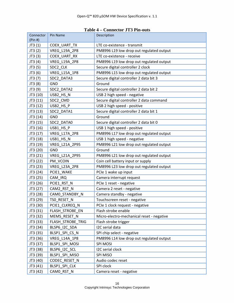
Table 4 – Connector JT3 Pin-outs Connector (Pin #)
Pin Name Description
JT3 (1) COEX_UART_TX LTE co-existence - transmit JT3 (2) VREG_L19A_2P8 PM8996 L19 low drop out regulated output JT3 (3) COEX_UART_RX LTE co-existence - receive JT3 (4) VREG_L19A_2P8 PM8996 L19 low drop out regulated output JT3 (5) SDC2_CLK Secure digital controller 2 clock JT3 (6) VREG_L15A_1P8 PM8996 L15 low drop out regulated output JT3 (7) SDC2_DATA3 Secure digital controller 2 data bit 3 JT3 (8) GND Ground JT3 (9) SDC2_DATA2 Secure digital controller 2 data bit 2 JT3 (10) USB2_HS_N USB 2 high speed - negative JT3 (11) SDC2_CMD Secure digital controller 2 data command JT3 (12) USB2_HS_P USB 2 high speed - positive JT3 (13) SDC2_DATA1 Secure digital controller 2 data bit 1 JT3 (14) GND Ground JT3 (15) SDC2_DATA0 Secure digital controller 2 data bit 0 JT3 (16) USB1_HS_P USB 1 high speed - positive JT3 (17) VREG_L17A_2P8 PM8996 L17 low drop out regulated output JT3 (18) USB1_HS_N USB 1 high speed - negative JT3 (19) VREG_L21A_2P95 PM8996 L21 low drop out regulated output JT3 (20) GND Ground JT3 (21) VREG_L21A_2P95 PM8996 L21 low drop out regulated output JT3 (22) PM_VCOIN Coin cell battery input or supply JT3 (23) VREG_L23A_2P8 PM8996 L23 low drop out regulated output JT3 (24) PCIE1_WAKE PCIe 1 wake up input JT3 (25) CAM_IRQ Camera interrupt request JT3 (26) PCIE1_RST_N PCIe 1 reset - negative JT3 (27) CAM2_RST_N Camera 2 reset - negative JT3 (28) CAM0_STANDBY_N Camera standby - negative JT3 (29) TS0_RESET_N Touchscreen reset - negative JT3 (30) PCIE1_CLKREQ_N PCIe 1 clock request - negative JT3 (31) FLASH_STROBE_EN Flash strobe enable JT3 (32) MEMS_RESET_N Micro-electro-mechanical reset - negative JT3 (33) FLASH_STROBE_TRIG Flash strobe trigger JT3 (34) BLSP6_I2C_SDA I2C serial data JT3 (35) BLSP1_SPI_CS_N SPI chip select - negative JT3 (36) VREG_L14A_1P8 PM8996 L14 low drop out regulated output JT3 (37) BLSP1_SPI_MOSI SPI MOSI JT3 (38) BLSP6_I2C_SCL I2C serial clock JT3 (39) BLSP1_SPI_MISO SPI MISO JT3 (40) CODEC_RESET_N Audio codec reset JT3 (41) BLSP1_SPI_CLK SPI clock JT3 (42) CAM0_RST_N Camera reset - negative
Open-Q™ 820 μSOM HW Device Specification v. 1.1
17 Copyright Intrinsyc Technologies Corporation
Connector (Pin #)
Pin Name Description
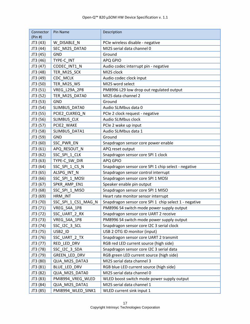
JT3 (43) W_DISABLE_N PCIe wireless disable - negative JT3 (44) SEC_MI2S_DATA0 MI2S serial data channel 0 JT3 (45) GND Ground JT3 (46) TYPE-C_INT APQ GPIO JT3 (47) CODEC_INT1_N Audio codec interrupt pin - negative JT3 (48) TER_MI2S_SCK MI2S clock JT3 (49) CDC_MCLK Audio codec clock input JT3 (50) TER_MI2S_WS MI2S word select JT3 (51) VREG_L29A_2P8 PM8996 L29 low drop out regulated output JT3 (52) TER_MI2S_DATA0 MI2S data channel 2 JT3 (53) GND Ground JT3 (54) SLIMBUS_DATA0 Audio SLIMbus data 0 JT3 (55) PCIE2_CLKREQ_N PCIe 2 clock request - negative JT3 (56) SLIMBUS_CLK Audio SLIMbus clock JT3 (57) PCIE2_WAKE PCIe 2 wake up input JT3 (58) SLIMBUS_DATA1 Audio SLIMbus data 1 JT3 (59) GND Ground JT3 (60) SSC_PWR_EN Snapdragon sensor core power enable JT3 (61) APQ_RESOUT_N APQ reset output JT3 (62) SSC_SPI_1_CLK Snapdragon sensor core SPI 1 clock JT3 (63) TYPE-C_SW_DIR APQ GPIO JT3 (64) SSC_SPI_1_CS_N Snapdragon sensor core SPI 1 chip select - negative JT3 (65) ALSPG_INT_N Snapdragon sensor control interrupt JT3 (66) SSC_SPI_1_MOSI Snapdragon sensor core SPI 1 MOSI JT3 (67) SPKR_AMP_EN1 Speaker enable pin output JT3 (68) SSC_SPI_1_MISO Snapdragon sensor core SPI 1 MISO JT3 (69) HRM_INT Heart rate monitor sensor interrupt JT3 (70) SSC_SPI_1_CS1_MAG_N Snapdragon sensor core SPI 1 chip select 1 - negative JT3 (71) VREG_S4A_1P8 PM8996 S4 switch mode power supply output JT3 (72) SSC_UART_2_RX Snapdragon sensor core UART 2 receive JT3 (73) VREG_S4A_1P8 PM8996 S4 switch mode power supply output JT3 (74) SSC_I2C_3_SCL Snapdragon sensor core I2C 3 serial clock JT3 (75) USB2_ID USB 2 OTG ID monitor (input) JT3 (76) SSC_UART_2_TX Snapdragon sensor core UART 2 transmit JT3 (77) RED_LED_DRV RGB red LED current source (high side) JT3 (78) SSC_I2C_3_SDA Snapdragon sensor core I2C 3 serial data JT3 (79) GREEN_LED_DRV RGB green LED current source (high side) JT3 (80) QUA_MI2S_DATA3 MI2S serial data channel 3 JT3 (81) BLUE_LED_DRV RGB blue LED current source (high side) JT3 (82) QUA_MI2S_DATA0 MI2S serial data channel 0 JT3 (83) PMI8994_VREG_WLED WLED boost switch mode power supply output JT3 (84) QUA_MI2S_DATA1 MI2S serial data channel 1 JT3 (85) PMI8994_WLED_SINK1 WLED current sink input 1
Open-Q™ 820 μSOM HW Device Specification v. 1.1
18 Copyright Intrinsyc Technologies Corporation
Connector (Pin #)
Pin Name Description
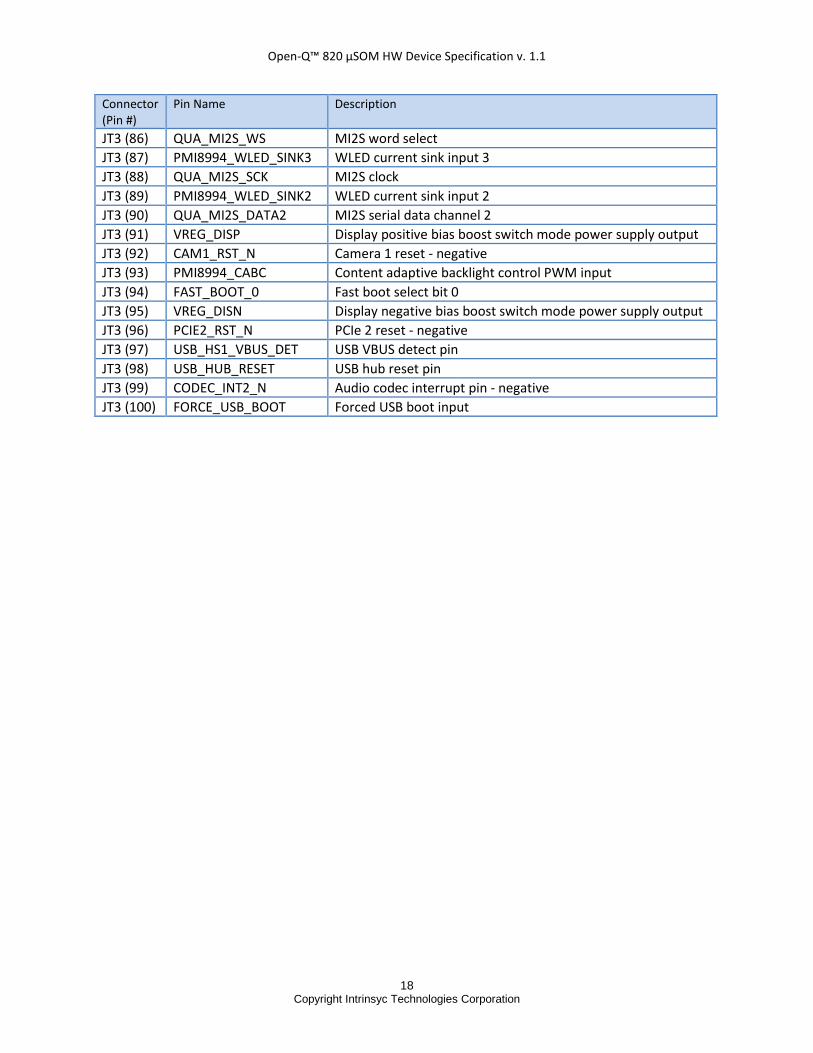
JT3 (86) QUA_MI2S_WS MI2S word select JT3 (87) PMI8994_WLED_SINK3 WLED current sink input 3 JT3 (88) QUA_MI2S_SCK MI2S clock JT3 (89) PMI8994_WLED_SINK2 WLED current sink input 2 JT3 (90) QUA_MI2S_DATA2 MI2S serial data channel 2 JT3 (91) VREG_DISP Display positive bias boost switch mode power supply output JT3 (92) CAM1_RST_N Camera 1 reset - negative JT3 (93) PMI8994_CABC Content adaptive backlight control PWM input JT3 (94) FAST_BOOT_0 Fast boot select bit 0 JT3 (95) VREG_DISN Display negative bias boost switch mode power supply output JT3 (96) PCIE2_RST_N PCIe 2 reset - negative JT3 (97) USB_HS1_VBUS_DET USB VBUS detect pin JT3 (98) USB_HUB_RESET USB hub reset pin JT3 (99) CODEC_INT2_N Audio codec interrupt pin - negative JT3 (100) FORCE_USB_BOOT Forced USB boot input
Open-Q™ 820 μSOM HW Device Specification v. 1.1
19 Copyright Intrinsyc Technologies Corporation
5. ELECTRICAL SPECIFICATIONS The input power to the µSOM is provided by a power supply (battery or wall adapter) and also a USB source, for battery charging purposes. All input power sources enter the PMI8996, which then distributes power via LDOs and switching power supplies.
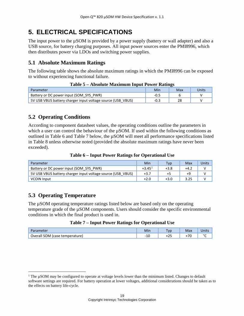
5.1 Absolute Maximum Ratings The following table shows the absolute maximum ratings in which the PMI8996 can be exposed to without experiencing functional failure.
Table 5 – Absolute Maximum Input Power Ratings Parameter Min Max Units Battery or DC power input (SOM_SYS_PWR) -0.5 6 V 5V USB VBUS battery charger input voltage source (USB_VBUS) -0.3 28 V
5.2 Operating Conditions According to component datasheet values, the operating conditions outline the parameters in which a user can control the behaviour of the µSOM. If used within the following conditions as outlined in Table 6 and Table 7 below, the µSOM will meet all performance specifications listed in Table 8 unless otherwise noted (provided the absolute maximum ratings have never been exceeded).
Table 6 – Input Power Ratings for Operational Use Parameter Min Typ Max Units Battery or DC power input (SOM_SYS_PWR) +3.451 +3.8 +4.2 V 5V USB VBUS battery charger input voltage source (USB_VBUS) +3.7 +5 +9 V VCOIN Input +2.0 +3.0 3.25 V
5.3 Operating Temperature The µSOM operating temperature ratings listed below are based only on the operating temperature grade of the µSOM components. Users should consider the specific environmental conditions in which the final product is used in.
Table 7 – Input Power Ratings for Operational Use Parameter Min Typ Max Units Overall SOM (case temperature) -10 +25 +70 °C
1 The µSOM may be configured to operate at voltage levels lower than the minimum listed. Changes to default software settings are required. For battery operation at lower voltages, additional considerations should be taken as to the effects on battery life-cycle.
Open-Q™ 820 μSOM HW Device Specification v. 1.1
20 Copyright Intrinsyc Technologies Corporation
5.4 Power Consumption
5.4.1 Setup and Methodology Power consumption measurements have been performed on the µSOM running Android under common operational modes. All tests were executed at room temperature and with the default thermal solution that ships with the µSOM development kit (heat sink on top of CPU) unless noted otherwise. In some test cases, as noted in the results section below, ADB was used to monitor the µSOM to ensure that the CPU was not throttling during the test. If ADB is not used, power consumption may be lower.
NOTE: Power consumption of the µSOM varies depending on the thermal solution used. A different thermal solution may result in allowing the CPU to run at higher average frequency but can cause overall power consumption to increase.
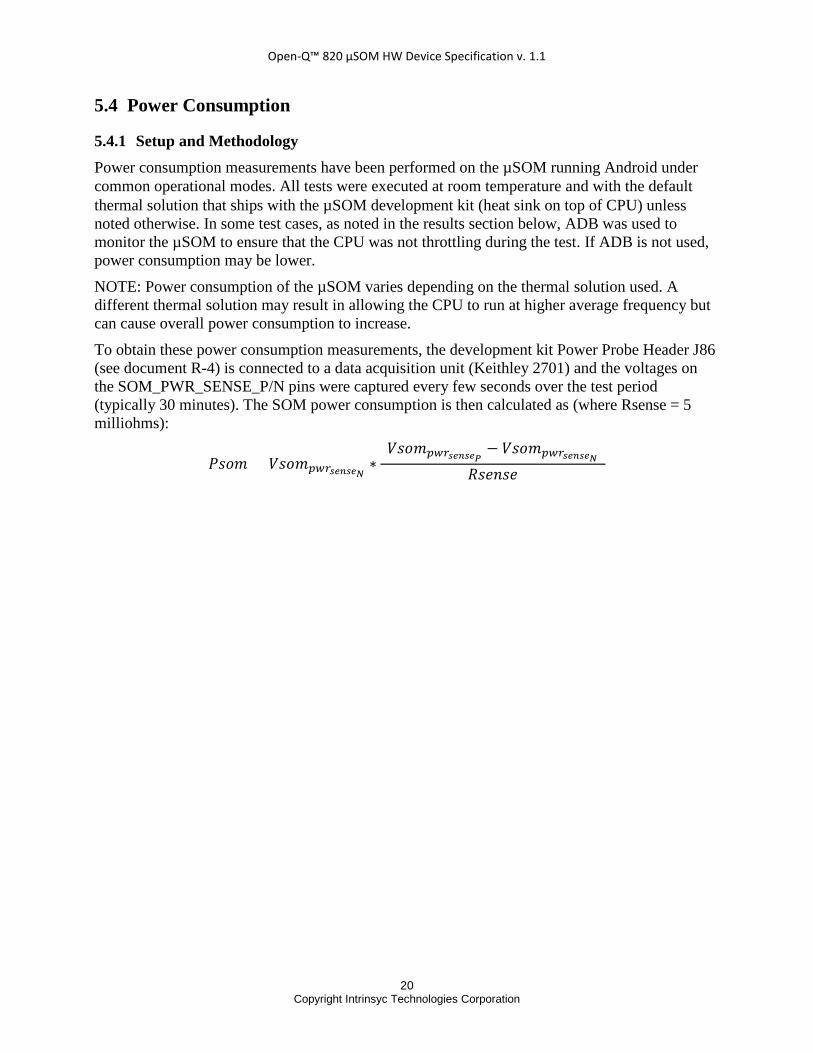
To obtain these power consumption measurements, the development kit Power Probe Header J86 (see document R-4) is connected to a data acquisition unit (Keithley 2701) and the voltages on the SOM_PWR_SENSE_P/N pins were captured every few seconds over the test period (typically 30 minutes). The SOM power consumption is then calculated as (where Rsense = 5 milliohms):
𝑃𝑃𝑃𝑃𝑃𝑃𝑃𝑃 = 𝑉𝑉𝑃𝑃𝑃𝑃𝑃𝑃𝑝𝑝𝑝𝑝𝑟𝑟𝑠𝑠𝑠𝑠𝑠𝑠𝑠𝑠𝑠𝑠𝑁𝑁∗
(𝑉𝑉𝑃𝑃𝑃𝑃𝑃𝑃𝑝𝑝𝑝𝑝𝑟𝑟𝑠𝑠𝑠𝑠𝑠𝑠𝑠𝑠𝑠𝑠𝑃𝑃− 𝑉𝑉𝑃𝑃𝑃𝑃𝑃𝑃𝑝𝑝𝑝𝑝𝑟𝑟𝑠𝑠𝑠𝑠𝑠𝑠𝑠𝑠𝑠𝑠𝑁𝑁
)𝑅𝑅𝑃𝑃𝑠𝑠𝑠𝑠𝑃𝑃𝑠𝑠
Open-Q™ 820 μSOM HW Device Specification v. 1.1
21 Copyright Intrinsyc Technologies Corporation
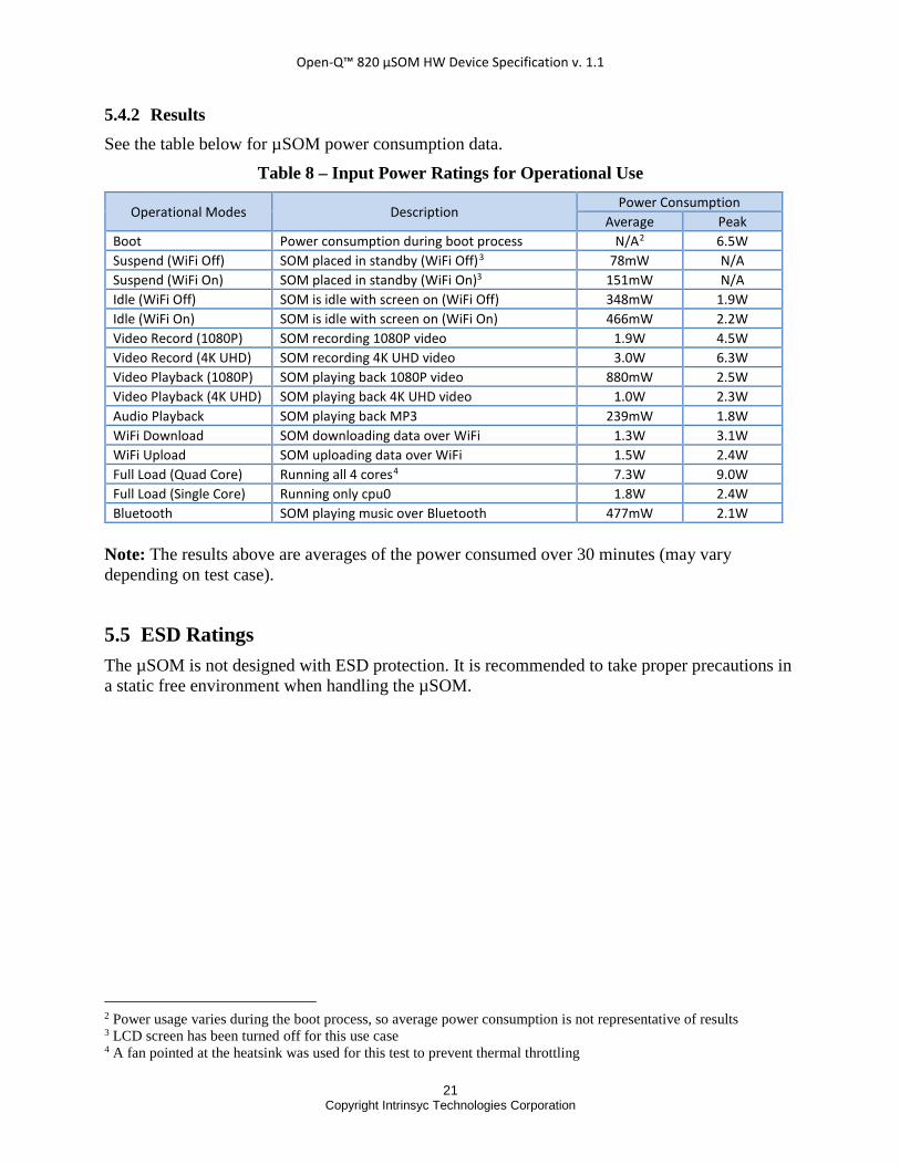
5.4.2 Results See the table below for µSOM power consumption data.
Table 8 – Input Power Ratings for Operational Use
Operational Modes Description Power Consumption
Average Peak Boot Power consumption during boot process N/A2 6.5W Suspend (WiFi Off) SOM placed in standby (WiFi Off)3 78mW N/A Suspend (WiFi On) SOM placed in standby (WiFi On)3 151mW N/A Idle (WiFi Off) SOM is idle with screen on (WiFi Off) 348mW 1.9W Idle (WiFi On) SOM is idle with screen on (WiFi On) 466mW 2.2W Video Record (1080P) SOM recording 1080P video 1.9W 4.5W Video Record (4K UHD) SOM recording 4K UHD video 3.0W 6.3W Video Playback (1080P) SOM playing back 1080P video 880mW 2.5W Video Playback (4K UHD) SOM playing back 4K UHD video 1.0W 2.3W Audio Playback SOM playing back MP3 239mW 1.8W WiFi Download SOM downloading data over WiFi 1.3W 3.1W WiFi Upload SOM uploading data over WiFi 1.5W 2.4W Full Load (Quad Core) Running all 4 cores4 7.3W 9.0W Full Load (Single Core) Running only cpu0 1.8W 2.4W Bluetooth SOM playing music over Bluetooth 477mW 2.1W
Note: The results above are averages of the power consumed over 30 minutes (may vary depending on test case).
5.5 ESD Ratings The µSOM is not designed with ESD protection. It is recommended to take proper precautions in a static free environment when handling the µSOM.
2 Power usage varies during the boot process, so average power consumption is not representative of results 3 LCD screen has been turned off for this use case 4 A fan pointed at the heatsink was used for this test to prevent thermal throttling
Open-Q™ 820 μSOM HW Device Specification v. 1.1
22 Copyright Intrinsyc Technologies Corporation
6. MECHANICAL SPECIFICATIONS
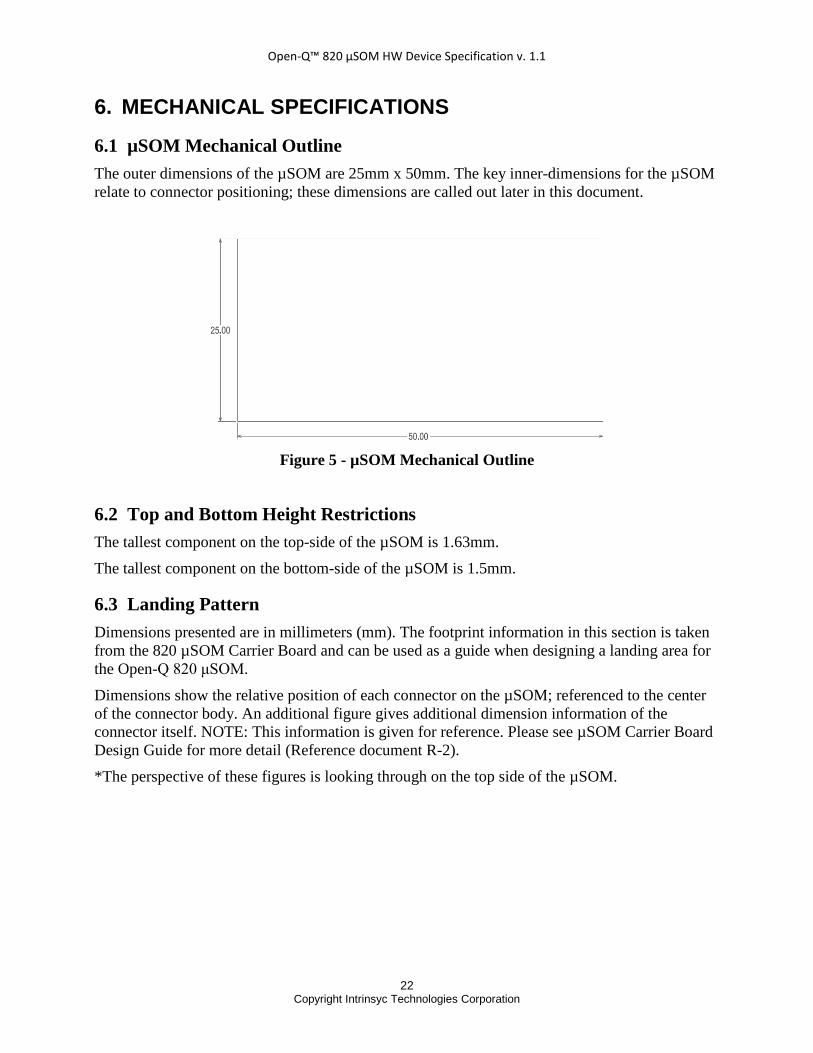
6.1 µSOM Mechanical Outline The outer dimensions of the µSOM are 25mm x 50mm. The key inner-dimensions for the µSOM relate to connector positioning; these dimensions are called out later in this document.
Figure 5 - µSOM Mechanical Outline
6.2 Top and Bottom Height Restrictions The tallest component on the top-side of the µSOM is 1.63mm.
The tallest component on the bottom-side of the µSOM is 1.5mm.
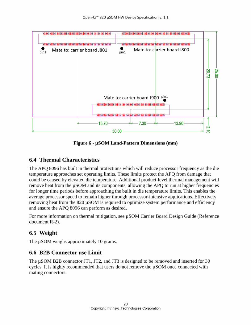
6.3 Landing Pattern Dimensions presented are in millimeters (mm). The footprint information in this section is taken from the 820 µSOM Carrier Board and can be used as a guide when designing a landing area for the Open-Q 820 μSOM.
Dimensions show the relative position of each connector on the µSOM; referenced to the center of the connector body. An additional figure gives additional dimension information of the connector itself. NOTE: This information is given for reference. Please see µSOM Carrier Board Design Guide for more detail (Reference document R-2).
*The perspective of these figures is looking through on the top side of the µSOM.
Open-Q™ 820 μSOM HW Device Specification v. 1.1
23 Copyright Intrinsyc Technologies Corporation
Figure 6 - µSOM Land-Pattern Dimensions (mm)
6.4 Thermal Characteristics The APQ 8096 has built in thermal protections which will reduce processor frequency as the die temperature approaches set operating limits. These limits protect the APQ from damage that could be caused by elevated die temperature. Additional product-level thermal management will remove heat from the µSOM and its components, allowing the APQ to run at higher frequencies for longer time periods before approaching the built in die temperature limits. This enables the average processor speed to remain higher through processor-intensive applications. Effectively removing heat from the 820 µSOM is required to optimize system performance and efficiency and ensure the APQ 8096 can perform as desired.
For more information on thermal mitigation, see µSOM Carrier Board Design Guide (Reference document R-2).
6.5 Weight The µSOM weighs approximately 10 grams.
6.6 B2B Connector use Limit The µSOM B2B connector JT1, JT2, and JT3 is designed to be removed and inserted for 30 cycles. It is highly recommended that users do not remove the µSOM once connected with mating connectors.
Open-Q™ 820 μSOM HW Device Specification v. 1.1
24 Copyright Intrinsyc Technologies Corporation
7. PRODUCT MARKING, ORDERING, AND STORAGE INFO
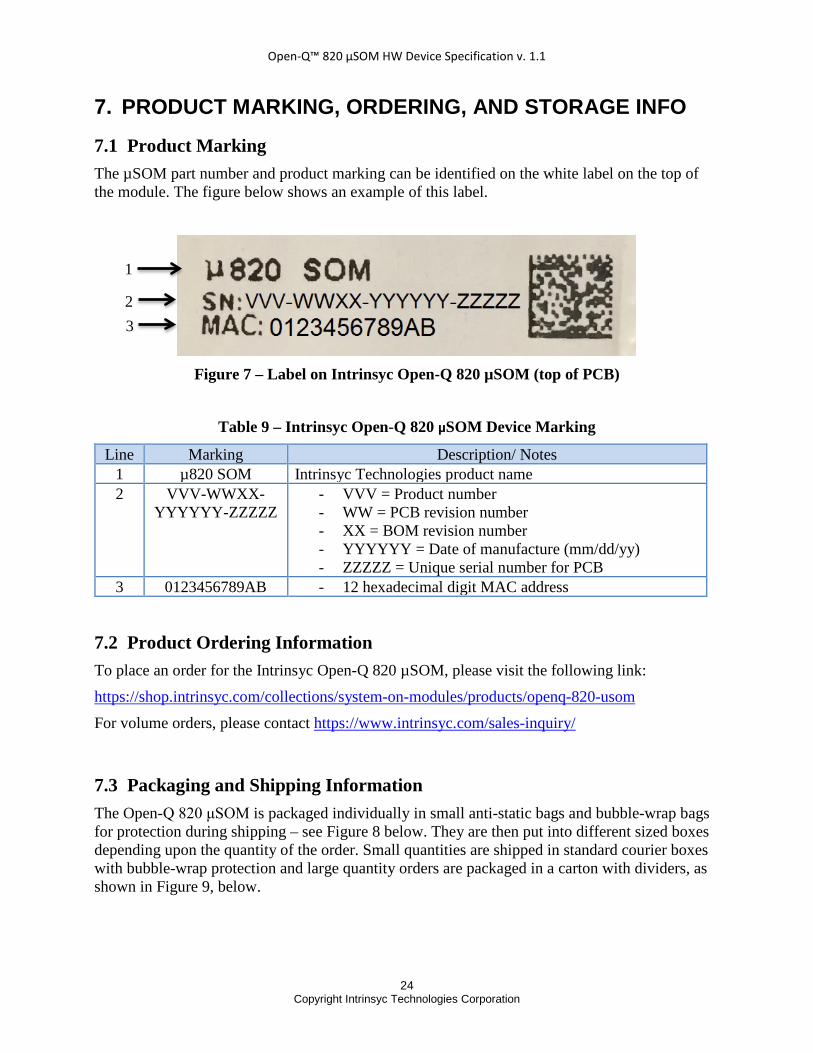
7.1 Product Marking The µSOM part number and product marking can be identified on the white label on the top of the module. The figure below shows an example of this label.
Figure 7 – Label on Intrinsyc Open-Q 820 µSOM (top of PCB)
Table 9 – Intrinsyc Open-Q 820 µSOM Device Marking
Line Marking Description/ Notes 1 µ820 SOM Intrinsyc Technologies product name 2 VVV-WWXX-
YYYYYY-ZZZZZ - VVV = Product number - WW = PCB revision number - XX = BOM revision number - YYYYYY = Date of manufacture (mm/dd/yy) - ZZZZZ = Unique serial number for PCB
3 0123456789AB - 12 hexadecimal digit MAC address
7.2 Product Ordering Information To place an order for the Intrinsyc Open-Q 820 µSOM, please visit the following link:
https://shop.intrinsyc.com/collections/system-on-modules/products/openq-820-usom
For volume orders, please contact https://www.intrinsyc.com/sales-inquiry/
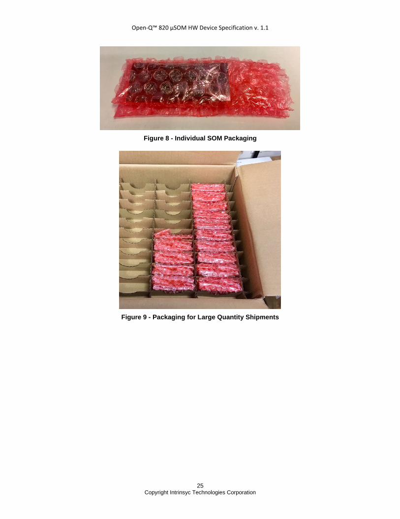
7.3 Packaging and Shipping Information The Open-Q 820 μSOM is packaged individually in small anti-static bags and bubble-wrap bags for protection during shipping – see Figure 8 below. They are then put into different sized boxes depending upon the quantity of the order. Small quantities are shipped in standard courier boxes with bubble-wrap protection and large quantity orders are packaged in a carton with dividers, as shown in Figure 9, below.
1
2 3
Open-Q™ 820 μSOM HW Device Specification v. 1.1
25 Copyright Intrinsyc Technologies Corporation
Figure 8 - Individual SOM Packaging
Figure 9 - Packaging for Large Quantity Shipments

Open-Q™ 820 μSOM HW Device Specification v. 1.1
26 Copyright Intrinsyc Technologies Corporation
8. HANDLING PRECAUTIONS
8.1 ESD Precautions Electrostatic discharge (ESD) occurs naturally in laboratory and factory environments. An established high-voltage potential is always at risk of discharging to a lower potential. If this discharge path is through a semiconductor device, destructive damage may result. The Open-Q 820 μSOM is designed as a component meant to be integrated into a final product and therefore has no additional ESD protection built-in. It should be handled only in a static-safe environment to prevent damage.
8.2 SOM – Carrier Board Mating Cautions Caution must be taken when connecting or disconnecting the SOM to a carrier board to prevent damage. Ensure that the SOM is inserted and removed straight up and down to prevent any sideways force on the connectors which could damage them. Also note that the DF40C-100DX board to board connectors are rated for a maximum of 30 mating / un-mating cycles. Therefore the number of insertions and removals must be limited to ensure reliability of the connectors.
8.3 Storage The µSOM must be stored in an antistatic bag.
Open-Q™ 820 μSOM HW Device Specification v. 1.1
27 Copyright Intrinsyc Technologies Corporation
9. CERTIFICATION
9.1 Radio Certification The Intrinsyc Open-Q 820 μSOM uses a pre-certified WLAN/BT module. The module is certified with FCC and Industry Canada as a modular radio transmitter for WLAN and Bluetooth.
FCC ID: 2AFDI-ITCNFA324.
Industry Canada ID: 9049A-ITCNFA324
The WLAN/BT module has also been tested to the applicable radio standards in many other countries:
- Australia
- Brazil
- China
- EU (CE Mark)
- India
- Japan
- Mexico
- New Zealand
- Singapore
- South Korea
- Taiwan
For more information or assistance in certifying your 820 uSOM based product please contact Intrinsyc at: https://www.intrinsyc.com/sales-inquiry/
9.2 ROHS/REACH Compliance The Intrinsyc Open-Q 820 µSOM comply with the ROHS/REACH standard. See the following link for information on ROHS/REACH certificate:
https://tech.intrinsyc.com/documents/306

Open-Q™ 820 μSOM HW Device Specification v. 1.1
28 Copyright Intrinsyc Technologies Corporation
10. COMPANY CONTACT
For more information, support, or sales, please contact us.
Company Contact: Intrinsyc Technologies Corporation,
885 Dunsmuir St. 3rd Floor
Vancouver, BC
Canada
V6C 1N5
Tel. (604) 801-6461
https://www.intrinsyc.com/
http://shop.intrinsyc.com
Sales: https://www.intrinsyc.com/sales-inquiry/
Support: https://helpdesk.intrinsyc.com/
Information: https://www.intrinsyc.com/resources/