nonvolatile unipolar memristive switching mechanism of pulse laser ablated nio films
TRANSCRIPT
Nonvolatile and unipolar resistive switching characteristics of pulsed laserablated NiO films
D. Panda,a� A. Dhar, and S. K. Raya�
Department of Physics and Meteorology, Indian Institute of Technology, Kharagpur 721302, India
�Received 22 September 2010; accepted 11 October 2010; published online 29 November 2010�
Unipolar nonvolatile resistive switching memory properties of pulse laser ablated nickel oxide filmshave been studied. Grazing incidence x-ray diffraction and electron diffraction spectra of the oxidefilms reveal polycrystalline nature of deposited NiO films. Cross-sectional transmission electronmicrograph shows a fairly uniform oxide surface. The rms surface roughnesses of deposited oxideshave been studied as a function of annealing temperature using atomic force microscopy. Byapplying a proper voltage bias and compliance, Pt/NiO/Pt structures exhibited unipolar resistiveswitching having a very low SET and RESET voltages. The OFF state resistance and SET voltageare found to increase with the increase in annealing temperature. The ratio between the tworesistance states can be as high as 1000. The current conduction phenomena at two resistance stateshave been studied. The switching phenomena have been explained using the rupture and formationof conducting filaments. The effect of postdeposition annealing on the resistance switchingproperties is discussed. © 2010 American Institute of Physics. �doi:10.1063/1.3514036�
I. INTRODUCTION
Different kinds of nonvolatile memory devices haveemerged over the last few decades, although all have sometechnical limits, such as higher switching power, retentivity,scalability, and reliability aspects.1–6 To overcome such con-straints, resistive switching memory devices,7–14 called mem-ristive device, first introduced as a fourth fundamental ele-ment in 1971,15 is one of the promising candidates for futurenanoscale memories. Such classes of switching devices areconductive bridge random access memory �CBRAM� �Ref.7� and resistive random access memory �RRAM�.8–30 Mem-ristive device has the expected advantages of nonvolatility,fast programming, small bit cell size, and low power con-sumption. Memristive is a realistic and prospective alterna-tive because of its simple memory cell structure, lowfabrication-process temperature, and appropriate scalabilitydue to filamentary conductive path mechanism in the oxidefilm. Binary metal oxide based memristive structures usingTiO2, NiO, Ta2O5, SiO2, HfO2, Cu2O, etc.9–30 films are at-tractive for the embedded complementary metal-oxide-semiconductor �CMOS� logic memory circuits in terms ofprocess compatibility.
Memristive devices with bistable states consist of asandwich structure of the metal oxide between two elec-trodes. It was exhibits a high resistive state �HRS� and a lowresistive state �LRS� that can be achieved simply by applyingan appropriate voltage. In some cases, viz., Ta2O5 /Cu �Refs.8 and 9� and TiOx /TiN,12,18 the resistive state can bechanged from high to low �SET� or from low to high �RE-SET� by using a bipolar voltage pulse. Compared to bipolarvoltage switching, unipolar switching seems to be more pref-erable for practical applications, due to intricate peripheralcircuit design. Binary oxide materials, such as NiO and HfO2
exhibit bistable resistive states with a unipolar voltagesweep. Among them, NiO is most promising due to its highON/OFF ratio, simple constituents and compatibility withCMOS process.18–23,25–27 On the other hand, pulsed laserdeposition �PLD� provides an unique advantage for oxidefilm deposition and enables even epitaxial growth of the filmon a substrate. In PLD process factors, such as depositionrate, substrate temperature, lattice mismatch, and thermal ex-pansion difference between the film and the substrate alterthe structure of the deposited film.
In this paper, we report the fabrication and switchingcharacteristics of Pt/NiO/Pt memristive devices. The phaseformation of the nickel oxide films and its interface havebeen studied using x-ray diffraction �XRD� spectra, cross-sectional transmission electron microscopy �TEM�, and se-lected area electron diffraction �SAED�. The switching char-acteristics of the grown Pt/NiO/Pt memristive devices arereported.
II. EXPERIMENTAL DETAILS
NiO films were grown by PLD �KrF excimer laser,Lambda Physik, 248 nm� on Pt /Ti /SiO2 /Si substrates. Pt�50 nm� and Ti �20 nm� were deposited by rf and dc magne-tron sputtering, respectively, on thermally grown SiO2. A la-ser beam of energy density 2.8 J /cm2 with 10 Hz repeat ratewas used to ablate from the sintered Ni target. The oxygenprocess pressure, target-to-substrate distance, and number oflaser shots were maintained to be 0.5 mbar, 2.5 cm, and60 000, respectively, during deposition. Whereas the sub-strate temperature was varied from 200 to 600 °C and thetarget was simultaneously rotated and translated. The post-deposition annealing �PDA� was performed in pure oxygenambient from 200 to 500 °C for 30 min to study the anneal-ing effect of the films. After NiO electrolyte deposition, a 50nm thin Pt top electrode was sputtered using a metal shadowmask �area: 2�10−4 cm2�. Grazing incidence �1°� XRD
a�Electronic addresses: [email protected] [email protected].
JOURNAL OF APPLIED PHYSICS 108, 104513 �2010�
0021-8979/2010/108�10�/104513/7/$30.00 © 2010 American Institute of Physics108, 104513-1
Author complimentary copy. Redistribution subject to AIP license or copyright, see http://jap.aip.org/jap/copyright.jsp
measurements, using Philips X’Pert Pro MRD diffracto-meter, was carried out to ascertain the crystallographic struc-ture of transition metal oxide. Cross-sectional high-resolution TEM �HRXTEM� with energy dispersive x-ray�EDX� analysis was carried out using a JEOL JEM-2100Fsystem operated at 200 kV to probe the thickness and uni-formity of the grown binary oxide films. The surface mor-phology of fabricated nickel oxide films was analyzed byatomic force microscopy �AFM�, using Veeco, Nanoscope-IV, in tapping mode. Electrical current-voltage �I-V� charac-teristics were performed using Keithley 4200 semiconductorcharacterization systems to study the switching behavior ofthe fabricated memristive devices.
III. RESULTS AND DISCUSSION
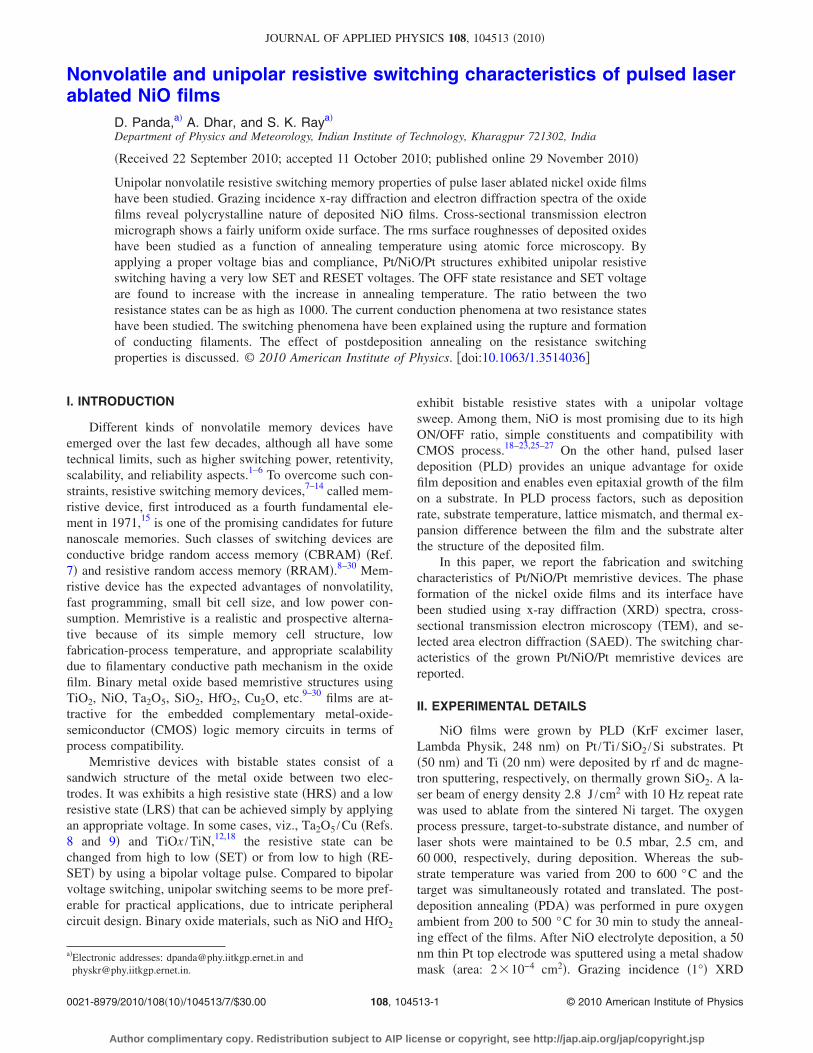
Figure 1 shows the typical grazing incident XRD spectraof the oxide films prepared at different substrate tempera-tures. Using Bragg’s condition, the lattice planes correspond-ing to each peak appearing from binary nickel oxide filmshave been calculated and compared with the standard dataavailable in ICDD files. A few strong nickel oxide phaseshaving cubic bunsenite structure of NiO are also observedfor the samples deposited at 400 and 600 °C substrate tem-peratures. Some volatile nickel oxide �NiO �110� and NiO2
�018�� phases also observed for the samples deposited atroom temperature. These phases are absent, when thesamples were deposited at an elevated substrate temperatureand also on PDA. From the XRD spectra, NiO films, depos-ited at an elevated substrate temperature, are found to bepolycrystalline, having �111�, �012�, �200�, and �220� orien-tations.
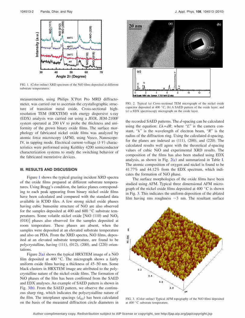
Figure 2�a� shows the typical HRXTEM image of a NiOfilm deposited at 400 °C. The micrograph shows a fairlyuniform oxide films having a thickness of 45–50 nm. Someblack clusters in HRXTEM image are attributed to the poly-crystalline nature of the nickel oxide films. The formation ofNiO phases of the film has been confirmed from the SAEDand EDX analyses. An example of SAED pattern is shown inFig. 3�b�. From the SAED pattern, we observe the continu-ous sharp ring, which indicates the polycrystalline nature ofthe film. The interplaner spacings �dhkl� has been calculatedon the basis of the measured diffraction circle diameters in
the recorded SAED patterns. The d-spacing can be calculatedusing the equation: L�=dR; where “L” is the camera con-stant, “�” is the wavelength of electron beam, “R” is theradius of the diffraction ring. Using the calculated d-spacing,for the planes are indexed as �111�, �200�, and �220�. Thecalculated results well agree with the theoretical d-spacingvalues of cubic NiO and experimental XRD results. Thecomposition of the films has also been studied using EDXanalysis, as shown in Fig. 2�c� and summarized in Table I.The atomic composition of oxygen and nickel is found to be41.77% and 44.12% from the EDX spectrum, which indi-cates the formation of NiO phase.
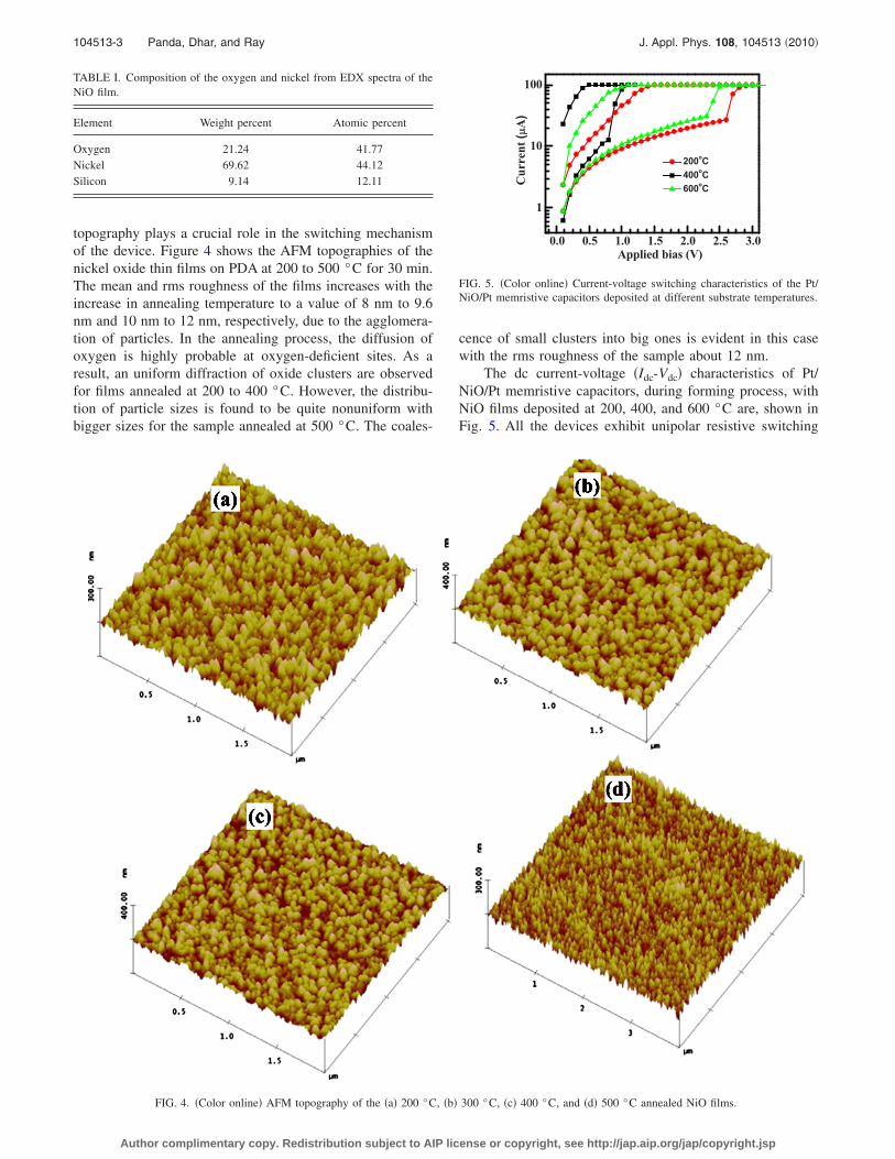
The surface morphologies of the oxide films have beenstudied using AFM. Typical three dimensional AFM micro-graph of the nickel oxide films deposited at 400 °C is shownin Fig. 3. This indicates the uniform deposition of the ablatedfilm having rms roughness �3 nm. The resultant surface
!"
! "! #! $! %!
&'(
*+!!,
$!!-.
"!!-.
+!!-.
/0
&'(
*111,
&'(
+*!12,
&'(
*++!,
&'(
*11!,
345647
'58*9:;:,
<4=>6 + *?6=@66,
&'(
*!1+,
FIG. 1. �Color online� XRD spectrum of the NiO films deposited at differentsubstrate temperatures.
FIG. 2. Typical �a� Cross-sectional TEM micrograph of the nickel oxidecapacitor deposited at 400 °C; �b� A SAED pattern of the oxide layer; and�c� a EDX spectroscopy micrograph on the oxide layer.
FIG. 3. �Color online� Typical AFM topography of the NiO films depositedat 400 °C substrate temperature.
104513-2 Panda, Dhar, and Ray J. Appl. Phys. 108, 104513 �2010�
Author complimentary copy. Redistribution subject to AIP license or copyright, see http://jap.aip.org/jap/copyright.jsp
topography plays a crucial role in the switching mechanismof the device. Figure 4 shows the AFM topographies of thenickel oxide thin films on PDA at 200 to 500 °C for 30 min.The mean and rms roughness of the films increases with theincrease in annealing temperature to a value of 8 nm to 9.6nm and 10 nm to 12 nm, respectively, due to the agglomera-tion of particles. In the annealing process, the diffusion ofoxygen is highly probable at oxygen-deficient sites. As aresult, an uniform diffraction of oxide clusters are observedfor films annealed at 200 to 400 °C. However, the distribu-tion of particle sizes is found to be quite nonuniform withbigger sizes for the sample annealed at 500 °C. The coales-
cence of small clusters into big ones is evident in this casewith the rms roughness of the sample about 12 nm.
The dc current-voltage �Idc-Vdc� characteristics of Pt/NiO/Pt memristive capacitors, during forming process, withNiO films deposited at 200, 400, and 600 °C are, shown inFig. 5. All the devices exhibit unipolar resistive switching
TABLE I. Composition of the oxygen and nickel from EDX spectra of theNiO film.
Element Weight percent Atomic percent
Oxygen 21.24 41.77Nickel 69.62 44.12Silicon 9.14 12.11
FIG. 4. �Color online� AFM topography of the �a� 200 °C, �b� 300 °C, �c� 400 °C, and �d� 500 °C annealed NiO films.
0.0 0.5 1.0 1.5 2.0 2.5 3.0
1
10
100
Applied bias (V)
Current(μμA)
200oC400oC600oC
FIG. 5. �Color online� Current-voltage switching characteristics of the Pt/NiO/Pt memristive capacitors deposited at different substrate temperatures.
104513-3 Panda, Dhar, and Ray J. Appl. Phys. 108, 104513 �2010�
Author complimentary copy. Redistribution subject to AIP license or copyright, see http://jap.aip.org/jap/copyright.jsp
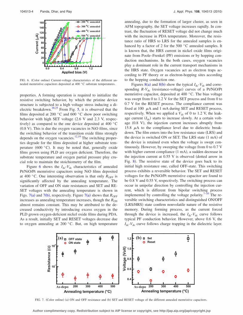
properties. A forming operation is required to initialize theresistive switching behavior, by which the pristine devicestructure is subjected to a high voltage stress inducing a di-electric breakdown.20,25 From Fig. 5, it is observed that thefilms deposited at 200 °C and 600 °C show poor switchingbehavior with high SET voltage �2.6 V and 2.3 V, respec-tively� as compared to the one device deposited at 400 °C�0.8 V�. This is due the oxygen vacancies in NiO films, sincethe switching behavior of the transition oxide films stronglydepends on the oxygen vacancies.12,19 The switching proper-ties degrade for the films deposited at higher substrate tem-perature �600 °C�. It may be noted that, generally oxidefilms grown using PLD are oxygen deficient. Therefore, thesubstrate temperature and oxygen partial pressure play cru-cial role to maintain the stoichiometry of the film.
Figure 6 shows the Idc-Vdc characteristics of annealedPt/NiO/Pt memristive capacitors using NiO films depositedat 400 °C. One interesting observation is that only ROFF issignificantly affected by the annealing temperature. Thevariation of OFF and ON state resistances and SET and RE-SET voltages with the annealing temperature is shown inFigs. 7�a� and 7�b�, respectively. Figure 7�a� shows that ROFF
increases as annealing temperature increases, though the RON
almost remains constant. This may be attributed to the de-creased conductivity by introducing excess oxygen in thePLD grown oxygen-deficient nickel oxide films during PDA.As a result, initially SET and RESET voltages decrease dueto oxygen annealing at 200 °C. But, on high temperature
annealing, due to the formation of larger cluster, as seen inAFM topography, the SET voltage increases rapidly. In con-trast, the fluctuation of RESET voltage did not change muchwith the increase in PDA temperature. Moreover, the resis-tance ratio of HRS to LRS for the annealed samples is en-hanced by a factor of 2 for the 500 °C annealed samples. Itis known that, the HRS current in nickel oxide films origi-nate from Poole–Frenkel �PF� emissions or by hopping con-duction mechanisms. In the both cases, oxygen vacanciesplay a dominant role in the current transport mechanisms inthe HRS state. Oxygen vacancies act as electron traps ac-cording to PF theory or as electron-hopping sites accordingto the hopping conduction one.
Figures 8�a� and 8�b� show the typical Idc-Vdc and corre-sponding R-Vdc �resistance-voltage� curves of a Pt/NiO/Ptmemristive capacitor, deposited at 400 °C. The bias voltagewas swept from 0 to 1.2 V for the SET process and from 0 to0.7 V for the RESET process. The compliance current wasfixed at 100 �A and 1 mA during SET and RESET process,respectively. When we applied a Vdc of 0 to 1.2 V, the leak-age current �Idc� starts to increase slowly. At a certain volt-age �0.8 V�, the injection current increases abruptly from15.8 �A to the compliance level due to dielectric break-down. The film enters into the low resistance state �LRS� andthe device is switched ON or SET. The LRS state �1 mA� ofthe device is retained even when the voltage is swept con-tinuously. However, by sweeping the voltage from 0 to 0.7 Vwith higher current compliance �1 mA�, a sudden decrease inthe injection current at 0.55 V is observed �dotted arrow inFig. 8�. The resistive state of the device goes back to itsinitial high resistance one, called OFF-state. This switchingprocess exhibits a reversible behavior. The SET and RESETvoltages for the Pt/NiO/Pt memristive capacitor are found tobe 0.8 V and 0.55 V, respectively. The switching process canoccur in unipolar direction by controlling the injection cur-rent, which is different from bipolar switching processimplemented by controlling the voltage polarity.7–10 The re-versible switching characteristics and distinguished ON/OFF�LRS/HRS� state confirm nonvolatile nature of the resistivememory. During forming process, as the current forcedthrough the device is increased, the Idc-Vdc curve followstypical PF conduction behavior. However, above 0.6 V, theIdc-Vdc curve follows charge trapping in the dielectric layer.
0.0 0.4 0.8 1.2
0
20
40
60
80
100
120
140
160
Current(μμA)
Applied bias (V)
200 oC annealed
300 oC annealed
400 oC annealed
500 oC annealed
FIG. 6. �Color online� Current-voltage characteristics of the different an-nealed memristive capacitors deposited at 400 °C substrate temperatures.
100 200 300 400 500
107
108
OFF stateON state
Resistance(ΩΩ)
Annealing temperature (°C)As-depo
(a)
100 200 300 400 500
0.4
0.6
0.8
1.0
1.2
Annealing temperature (°C)
SetReset
Voltage(Volt)
As-depo
(b)
FIG. 7. �Color online� �a� ON and OFF resistance and �b� SET and RESET voltage of the different annealed memristive capacitors.
104513-4 Panda, Dhar, and Ray J. Appl. Phys. 108, 104513 �2010�
Author complimentary copy. Redistribution subject to AIP license or copyright, see http://jap.aip.org/jap/copyright.jsp
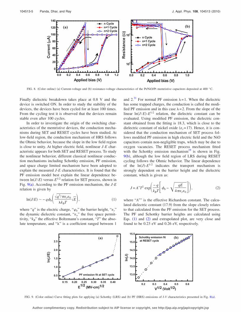
Finally dielectric breakdown takes place at 0.8 V and thedevice is switched ON. In order to study the stability of thedevices, the devices have been cycled for at least 100 times.From the cycling test it is observed that the devices remainstable even after 100 cycles.
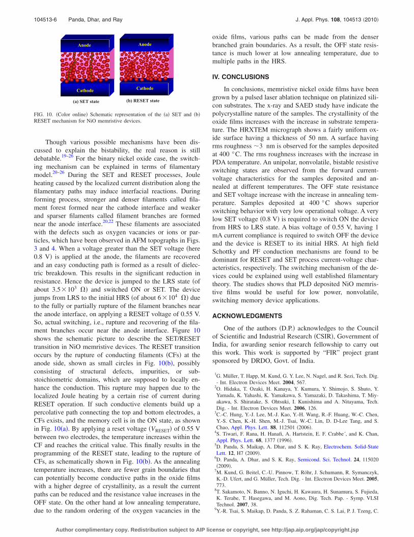
In order to investigate the origin of the switching char-acteristics of the memristive devices, the conduction mecha-nisms during SET and RESET cycles have been studied. Atlow-field region, the conduction mechanism of HRS followsthe Ohmic behavior, because the slope in the low field regionis close to unity. At higher electric field, nonlinear J-E char-acteristic appears for both SET and RESET process. To studythe nonlinear behavior, different classical nonlinear conduc-tion mechanisms including Schottky emission, PF emission,and space charge limited mechanism have been adopted toexplain the measured J-E characteristics. It is found that thePF emission model best explain the linear dependence be-tween ln�J /E� versus E1/2 relation for SET process, shown inFig. 9�a�. According to the PF emission mechanism, the J-Erelation is given by
ln�J/E� � − q�b��q3/��r�0
�kBT�E , �1�
where “q” is the electric charge, “�b” the barrier height, “�r”the dynamic dielectric constant, “�o” the free space permit-tivity, “kB” the effective Boltzmann’s constant, “T” the abso-lute temperature, and “�” is a coefficient ranged between 1
and 2.31 For normal PF emission �=1. When the dielectrichas some trapped charges, the conduction is called the modi-fied PF emission and in this case �=2. From the slope of thelinear ln�J /E�-E1/2 relation, the dielectric constant can beevaluated. Using modified PF emission, the dielectric con-stant obtained from the fitting is 18.3, which is close to thedielectric constant of nickel oxide ��r=17�. Hence, it is con-sidered that the conduction mechanism of SET process fol-lows modified PF emission in high electric field and the NiOcapacitors contain non-negligible traps, which may be due tooxygen vacancies. The RESET process mechanism fittedwith the Schottky emission mechanism19 is shown in Fig.9�b�, although the low field region of LRS during RESETcycling follows the Ohmic behavior. The linear dependenceof the ln�J�-E1/2 indicates the transport mechanism isstrongly dependent on the barrier height and the dielectricconstant, which is given as:
J = A�T2 exp� − q
kBT�b −� qE
4��r�0� , �2�
where “A�” is the effective Richardson constant. The calcu-lated dielectric constant �17.9� from the slope closely relatesto that calculated from the PF emission for the SET process.The PF and Schottky barrier heights are calculated usingEqs. �1� and �2� and extrapolated plot, are very close andfound to be 0.23 eV and 0.26 eV, respectively.
0.0 0.2 0.4 0.6 0.8 1.0 1.2
0
20
40
60
80
100
120
140
Current(μμA)
Applied bias (V)
n Cyclen+1 Cyclen+2 Cycle
(a)
0.0 0.2 0.4 0.6 0.8 1.0
105
104
Resistance(ΩΩ)
Applied bias (V)
n Cyclen+1 Cyclen+2 Cycle
(b)
FIG. 8. �Color online� �a� Current-voltage and �b� resistance-voltage characteristics of the Pt/NiO/Pt memristive capacitors deposited at 400 °C.
0.15 0.20 0.25 0.30 0.35 0.40
0.5
1.0
1.5
2.0
2.5
ln(J/E)
E1/2 (MV-cm)1/2
PF emission fit at SET cycle
(a)
0.2 0.3 0.4 0.5 0.6
13.0
13.5
14.0
14.5
15.0
15.5
ln(J)
V1/2 (Volt1/2)
Schottky emission fitat RESET cycle
(b)
FIG. 9. �Color online� Curve fitting plots for applying �a� Schottky �LRS� and �b� PF �HRS� emissions of I-V characteristics presented in Fig. 8�a�.
104513-5 Panda, Dhar, and Ray J. Appl. Phys. 108, 104513 �2010�
Author complimentary copy. Redistribution subject to AIP license or copyright, see http://jap.aip.org/jap/copyright.jsp
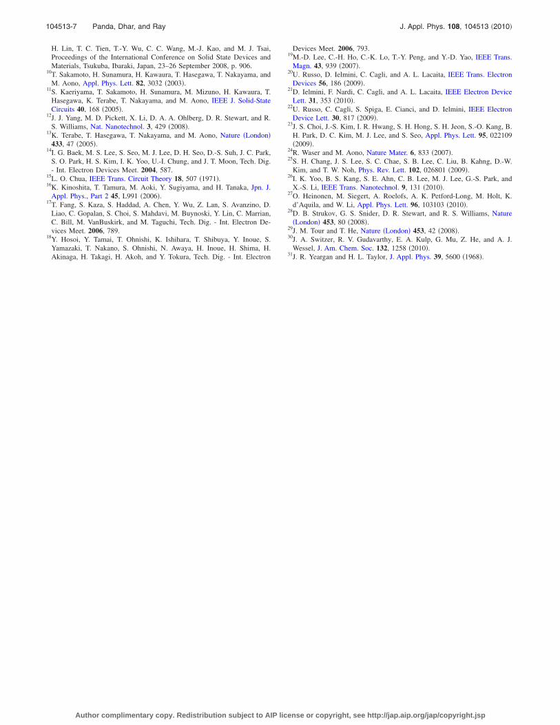
Though various possible mechanisms have been dis-cussed to explain the bistability, the real reason is stilldebatable.19–26 For the binary nickel oxide case, the switch-ing mechanism can be explained in terms of filamentarymodel.20–26 During the SET and RESET processes, Jouleheating caused by the localized current distribution along thefilamentary paths may induce interfacial reactions. Duringforming process, stronger and denser filaments called fila-ment forest formed near the cathode interface and weakerand sparser filaments called filament branches are formednear the anode interface.20,22 These filaments are associatedwith the defects such as oxygen vacancies or ions or par-ticles, which have been observed in AFM topographs in Figs.3 and 4. When a voltage greater than the SET voltage �here0.8 V� is applied at the anode, the filaments are recoveredand an easy conducting path is formed as a result of dielec-tric breakdown. This results in the significant reduction inresistance. Hence the device is jumped to the LRS state �ofabout 3.5�103 � and switched ON or SET. The devicejumps from LRS to the initial HRS �of about 6�104 � dueto the fully or partially rupture of the filament branches nearthe anode interface, on applying a RESET voltage of 0.55 V.So, actual switching, i.e., rupture and recovering of the fila-ment branches occur near the anode interface. Figure 10shows the schematic picture to describe the SET/RESETtransition in NiO memristive devices. The RESET transitionoccurs by the rupture of conducting filaments �CFs� at theanode side, shown as small circles in Fig. 10�b�, possiblyconsisting of structural defects, impurities, or sub-stoichiometric domains, which are supposed to locally en-hance the conduction. This rupture may happen due to thelocalized Joule heating by a certain rise of current duringRESET operation. If such conductive elements build up apercolative path connecting the top and bottom electrodes, aCFs exists, and the memory cell is in the ON state, as shownin Fig. 10�a�. By applying a reset voltage �VRESET� of 0.55 Vbetween two electrodes, the temperature increases within theCF and reaches the critical value. This finally results in theprogramming of the RESET state, leading to the rupture ofCFs, as schematically shown in Fig. 10�b�. As the annealingtemperature increases, there are fewer grain boundaries thatcan potentially become conductive paths in the oxide filmswith a higher degree of crystallinity, as a result the currentpaths can be reduced and the resistance value increases in theOFF state. On the other hand at low annealing temperature,due to the random ordering of the oxygen vacancies in the
oxide films, various paths can be made from the denserbranched grain boundaries. As a result, the OFF state resis-tance is much lower at low annealing temperature, due tomultiple paths in the HRS.
IV. CONCLUSIONS
In conclusions, memristive nickel oxide films have beengrown by a pulsed laser ablation technique on platinized sili-con substrates. The x-ray and SAED study have indicate thepolycrystalline nature of the samples. The crystallinity of theoxide films increases with the increase in substrate tempera-ture. The HRXTEM micrograph shows a fairly uniform ox-ide surface having a thickness of 50 nm. A surface havingrms roughness �3 nm is observed for the samples depositedat 400 °C. The rms roughness increases with the increase inPDA temperature. An unipolar, nonvolatile, bistable resistiveswitching states are observed from the forward current-voltage characteristics for the samples deposited and an-nealed at different temperatures. The OFF state resistanceand SET voltage increase with the increase in annealing tem-perature. Samples deposited at 400 °C shows superiorswitching behavior with very low operational voltage. A verylow SET voltage �0.8 V� is required to switch ON the devicefrom HRS to LRS state. A bias voltage of 0.55 V, having 1mA current compliance is required to switch OFF the deviceand the device is RESET to its initial HRS. At high fieldSchottky and PF conduction mechanisms are found to bedominant for RESET and SET process current-voltage char-acteristics, respectively. The switching mechanism of the de-vices could be explained using well established filamentarytheory. The studies shows that PLD deposited NiO memris-tive films would be useful for low power, nonvolatile,switching memory device applications.
ACKNOWLEDGMENTS
One of the authors �D.P.� acknowledges to the Councilof Scientific and Industrial Research �CSIR�, Government ofIndia, for awarding senior research fellowship to carry outthis work. This work is supported by “FIR” project grantsponsored by DRDO, Govt. of India.
1G. Müller, T. Happ, M. Kund, G. Y. Lee, N. Nagel, and R. Sezi, Tech. Dig.- Int. Electron Devices Meet. 2004, 567.
2O. Hidaka, T. Ozaki, H. Kanaya, Y. Kumura, Y. Shimojo, S. Shuto, Y.Yamada, K. Yahashi, K. Yamakawa, S. Yamazaki, D. Takashima, T. Miy-akawa, S. Shiratake, S. Ohtsuki, I. Kunishima and A. Nitayama, Tech.Dig. - Int. Electron Devices Meet. 2006, 126.
3C.-C. Hung, Y.-J. Lee, M.-J. Kao, Y.-H. Wang, R.-F. Huang, W.-C. Chen,Y.-S. Chen, K.-H. Shen, M.-J. Tsai, W.-C. Lin, D. D-Lee Tang, and S.Chao, Appl. Phys. Lett. 88, 112501 �2006�.
4S. Tiwari, F. Rana, H. Hanafi, A. Hartstein, E. F. Crabbe´, and K. Chan,Appl. Phys. Lett. 68, 1377 �1996�.
5D. Panda, S. Maikap, A. Dhar, and S. K. Ray, Electrochem. Solid-StateLett. 12, H7 �2009�.
6D. Panda, A. Dhar, and S. K. Ray, Semicond. Sci. Technol. 24, 115020�2009�.
7M. Kund, G. Beitel, C.-U. Pinnow, T. Röhr, J. Schumann, R. Symanczyk,K.-D. Ufert, and G. Müller, Tech. Dig. - Int. Electron Devices Meet. 2005,773.
8T. Sakamoto, N. Banno, N. Iguchi, H. Kawaura, H. Sunamura, S. Fujieda,K. Terabe, T. Hasegawa, and M. Aono, Dig. Tech. Pap. - Symp. VLSITechnol. 2007, 38.
9Y.-R. Tsai, S. Maikap, D. Panda, S. Z. Rahaman, C. S. Lai, P. J. Tzeng, C.
(a) SET state
Anode
Cathode Cathode
Anode
(b) RESET state
FIG. 10. �Color online� Schematic representation of the �a� SET and �b�RESET mechanism for NiO memristive devices.
104513-6 Panda, Dhar, and Ray J. Appl. Phys. 108, 104513 �2010�
Author complimentary copy. Redistribution subject to AIP license or copyright, see http://jap.aip.org/jap/copyright.jsp
H. Lin, T. C. Tien, T.-Y. Wu, C. C. Wang, M.-J. Kao, and M. J. Tsai,Proceedings of the International Conference on Solid State Devices andMaterials, Tsukuba, Ibaraki, Japan, 23–26 September 2008, p. 906.
10T. Sakamoto, H. Sunamura, H. Kawaura, T. Hasegawa, T. Nakayama, andM. Aono, Appl. Phys. Lett. 82, 3032 �2003�.
11S. Kaeriyama, T. Sakamoto, H. Sunamura, M. Mizuno, H. Kawaura, T.Hasegawa, K. Terabe, T. Nakayama, and M. Aono, IEEE J. Solid-StateCircuits 40, 168 �2005�.
12J. J. Yang, M. D. Pickett, X. Li, D. A. A. Ohlberg, D. R. Stewart, and R.S. Williams, Nat. Nanotechnol. 3, 429 �2008�.
13K. Terabe, T. Hasegawa, T. Nakayama, and M. Aono, Nature �London�433, 47 �2005�.
14I. G. Baek, M. S. Lee, S. Seo, M. J. Lee, D. H. Seo, D.-S. Suh, J. C. Park,S. O. Park, H. S. Kim, I. K. Yoo, U.-I. Chung, and J. T. Moon, Tech. Dig.- Int. Electron Devices Meet. 2004, 587.
15L. O. Chua, IEEE Trans. Circuit Theory 18, 507 �1971�.16K. Kinoshita, T. Tamura, M. Aoki, Y. Sugiyama, and H. Tanaka, Jpn. J.
Appl. Phys., Part 2 45, L991 �2006�.17T. Fang, S. Kaza, S. Haddad, A. Chen, Y. Wu, Z. Lan, S. Avanzino, D.
Liao, C. Gopalan, S. Choi, S. Mahdavi, M. Buynoski, Y. Lin, C. Marrian,C. Bill, M. VanBuskirk, and M. Taguchi, Tech. Dig. - Int. Electron De-vices Meet. 2006, 789.
18Y. Hosoi, Y. Tamai, T. Ohnishi, K. Ishihara, T. Shibuya, Y. Inoue, S.Yamazaki, T. Nakano, S. Ohnishi, N. Awaya, H. Inoue, H. Shima, H.Akinaga, H. Takagi, H. Akoh, and Y. Tokura, Tech. Dig. - Int. Electron
Devices Meet. 2006, 793.19M.-D. Lee, C.-H. Ho, C.-K. Lo, T.-Y. Peng, and Y.-D. Yao, IEEE Trans.
Magn. 43, 939 �2007�.20U. Russo, D. Ielmini, C. Cagli, and A. L. Lacaita, IEEE Trans. Electron
Devices 56, 186 �2009�.21D. Ielmini, F. Nardi, C. Cagli, and A. L. Lacaita, IEEE Electron Device
Lett. 31, 353 �2010�.22U. Russo, C. Cagli, S. Spiga, E. Cianci, and D. Ielmini, IEEE Electron
Device Lett. 30, 817 �2009�.23J. S. Choi, J.-S. Kim, I. R. Hwang, S. H. Hong, S. H. Jeon, S.-O. Kang, B.
H. Park, D. C. Kim, M. J. Lee, and S. Seo, Appl. Phys. Lett. 95, 022109�2009�.
24R. Waser and M. Aono, Nature Mater. 6, 833 �2007�.25S. H. Chang, J. S. Lee, S. C. Chae, S. B. Lee, C. Liu, B. Kahng, D.-W.
Kim, and T. W. Noh, Phys. Rev. Lett. 102, 026801 �2009�.26I. K. Yoo, B. S. Kang, S. E. Ahn, C. B. Lee, M. J. Lee, G.-S. Park, and
X.-S. Li, IEEE Trans. Nanotechnol. 9, 131 �2010�.27O. Heinonen, M. Siegert, A. Roelofs, A. K. Petford-Long, M. Holt, K.
d’Aquila, and W. Li, Appl. Phys. Lett. 96, 103103 �2010�.28D. B. Strukov, G. S. Snider, D. R. Stewart, and R. S. Williams, Nature
�London� 453, 80 �2008�.29J. M. Tour and T. He, Nature �London� 453, 42 �2008�.30J. A. Switzer, R. V. Gudavarthy, E. A. Kulp, G. Mu, Z. He, and A. J.
Wessel, J. Am. Chem. Soc. 132, 1258 �2010�.31J. R. Yeargan and H. L. Taylor, J. Appl. Phys. 39, 5600 �1968�.
104513-7 Panda, Dhar, and Ray J. Appl. Phys. 108, 104513 �2010�
Author complimentary copy. Redistribution subject to AIP license or copyright, see http://jap.aip.org/jap/copyright.jsp