nanotube enhanced photoresponse of carbon modified (cm)-n-tio2 for efficient water splitting
TRANSCRIPT
ARTICLE IN PRESS
0927-0248/$ - se
doi:10.1016/j.so
�CorrespondE-mail addr
Solar Energy Materials & Solar Cells 91 (2007) 938–943
www.elsevier.com/locate/solmat
Nanotube enhanced photoresponse of carbon modified(CM)-n-TiO2 for efficient water splitting
Chengkun Xu, Yasser A. Shaban, William B. Ingler Jr., Shahed U.M. Khan�
Department of Chemistry and Biochemistry, Duquesne University, Pittsburgh, PA 15282, USA
Received 7 September 2006; accepted 12 February 2007
Available online 5 April 2007
Abstract
Carbon modified (CM)-n-TiO2 nanotube arrays were successfully synthesized by anodization of Ti metal sheet in fluoride solution and
subsequent annealing in air and natural gas flame oxidation. Both nanotube structure and carbon doping contributed to the
enhancement of photoresponse of n-TiO2. About two fold increase in photocurrent density was observed at undoped n-TiO2 nanotube
film compared to that at its undoped n-TiO2 flat thin film. Also, about eight fold increase in photocurrent density was observed at carbon
modified (CM)-n-TiO2 nanotube film compared to that at undoped n-TiO2 flat thin film. The sample prepared by anodization at 20V cell
voltage for 20 h followed by annealing in air at 500 1C for 1 h and natural gas flame oxidation at 820 1C for 18min produced highest
photocurrent density. It was found that the bandgap of n-TiO2 was reduced to 2.84 eV and an additional intragap band was introduced
in the gap at 1.30 eV above the valence band. The bandgap reduction and the new intragap band formation in CM-n-TiO2 extended its
utilization of solar energy up to the visible to infrared region.
r 2007 Elsevier B.V. All rights reserved.
Keywords: Solar hydrogen production; Photoelectrochemical; Carbon-modified; Titanium dioxide; Nanotube
1. Introduction
Titanium dioxide has been among the most promisingphotoanode materials for photoelectrochemical splitting ofwater to produce hydrogen fuel and attracted extensiveattention. In recent years, researchers doped TiO2 withnitrogen [1], carbon [2–5], and sulfur [6] attempting tomodify its bandgap so that it can absorb in the visibleregion of the solar spectrum. It was reported that thecarbon modified (CM)-n-TiO2 showed reduced bandgapenergy [2–5] and efficient water splitting [2], and carbondoping also introduces an additional intragap band intothe bandgap of TiO2 [3,5,10,11] which can be utilized toabsorb photons with energy even lower than the reducedTiO2 bandgap. However, the quantum efficiency ofCM-n-TiO2 needs further enhancement. On the otherhand, the fabrication technique of nanoscale TiO2 hasbeen well established. Mor et al. [7] and Park et al. [8]
e front matter r 2007 Elsevier B.V. All rights reserved.
lmat.2007.02.010
ing author. Tel.: +1 (412)396 1647; fax: +1(412)396 6682.
ess: [email protected] (S.U.M. Khan).
reported the fabrication of highly ordered TiO2 nanotubearray, while Tang et al. [9] reported the preparationof crystalline mesoporous TiO2. The nanostructuredTiO2 allows efficient light absorption and photogeneratedcarrier collection. [7] Shankar et al. [12] investigated theeffect of flame annealing on the spectral photoresponseof titania nanotubes and demonstrated the enhancementin the visible spectrum absorption and photocurrent due toflame annealing. However, in their study, the flameannealing was carried out at 1020 1C which is muchhigher than the optimum temperature of 820 1C observedin our lab. Such high temperature generally removessome carbon from the sample and thus reduces thephotoresponse.Given the sensitivity of CM-n-TiO2 to flame tempera-
ture, we prepared highly ordered n-TiO2 nanotube arrayfilm and further oxidized it in natural gas flame at optimumtemperature to incorporate carbon into it. Significantenhancement of the photoresponse of these carbonmodified (CM)-n-TiO2 nanotube films was observed inthis study.

ARTICLE IN PRESS
-1.0 -0.8 -0.6 -0.4 -0.2 0.0
0
2
4
6
8
10 4
3
2
1
Ph
oto
curr
ent
den
sity
(m
A/c
m2)
Measured Potential (V vs SCE)
Fig. 1. Photocurrent density at CM-n-TiO2 nanotube film electrodes
versus measured potential with a light intensity of 100mW/cm2 from a
150W xenon arc lamp with wavelength range of 250–2400 nm, run in 5M
KOH. 1—reference sample of n-TiO2 flat thin film (without carbon doping
and nanotube structure); 2—nanotube film of undoped n-TiO2; 3—CM-
n-TiO2 thin film (with carbon doping but no nanotube structure); 4—CM-
n-TiO2 nanotube film (with carbon doping).
C. Xu et al. / Solar Energy Materials & Solar Cells 91 (2007) 938–943 939
2. Experimental
The TiO2 nanotube array was fabricated by anodizationof titanium sheet in a fluoride-containing solution. Theelectrolyte solution consisted of 0.1M ammonium fluoride,1M ammonium hydrogen sulfate, and 0.2M triammoniumcitrate at pH 5. The anodization was performed at a cellvoltage of 20V for 20 h. Following the anodization, theTiO2 nanotube was subjected to annealing at 500 1C in airfor 1 h to induce its crystallinity and oxidation in naturalgas flame at 820 1C for 18min to incorporate carbon intothe nanotube TiO2. A reference TiO2 sample was preparedby annealing a Ti sheet in air at 500 1C for 1 h followed bycalcination at 820 1C in air for 18min in an electric oven.
The resulting films were characterized using X-raydiffraction (XRD) spectra and scanning electron micro-scopy (SEM). XRD spectra were collected on a PANaly-tical X’Pert Pro powder X-ray diffractometer. The scanswere made in the range from 281 to 701 (2y) operating at avoltage of 45 kV and a current of 40mA. SEM images ofthe CM-n-TiO2 films were obtained using Cam Scan series4 Scanning electron microscope. The carbon contents inthe films were determined from energy dispersed X-ray(EDX) analysis using an X-ray detector with ultrathinwindow which allows the carbon detection.
Photoelectrochemical measurements were performedusing an EG&G Scanning Potentiostat and a custom madeelectrochemical cell with a thin quartz window. The surfaceof the CM-n-TiO2 film electrode was illuminated with a150W xenon arc lamp (Hanovia via Bulbtronics). Thespectral distribution of the xenon lamp was foundcomparable to that of sunlight with wavelength rangingfrom 300 nm to above 2400 nm. The intensity of the lightwas measured with a digital radiometer (InternationalLight, model IL 1350). A Keithley multimeter was used tomonitor the photocurrent and measure electrode potentialat open circuit condition. Photocurrents were measuredusing a scan rate of 50 mV/sec. The measurements were runin a 5.0M KOH electrolyte solution.
3. Results and discussion
To determine the respective photoresponse of nanotubearray fabrication and carbon doping of n-TiO2 for watersplitting, we prepared following photoanode samples:(1) flat thin films without carbon doping (reference sample)prepared by annealing in air at 500 1C for 1 h and then inair at 820 1C for 18min using an electric tube furnace,(2) nanotube films prepared by anodization followed bycalcination in air at 500 1C for 1 h followed by oxidation inair at 820 1C for 18min using an electric tube furnace,(3) flat thin films with carbon doping prepared bycalcination of Ti sheet in air at 500 1C for 1 h followed byoxidation in natural gas flame at 820 1C for 18min and(4) nanotube films with carbon doping prepared byanodization followed by calcination in air at 500 1C for1 h and oxidation in natural gas flame at 820 1C for 18min.
The carbon contents in the samples 1, 2, 3, and 4 werefound to be 0, 0, 3.7, and 4.3 at%, respectively, from EDXmeasurements. Fig. 1 shows the photocurrent densityversus measured potential at these electrodes underillumination of 100mW/cm2 white light from a 150Wxenon lamp. Compared to reference undoped flat thin filmof n-TiO2 (curve 1), the photoresponse of undoped n-TiO2
nanotube arrays (curve 2) increased by a factor of nearlytwo. This enhancement can be attributed mainly to theincrease in the surface area of n-TiO2 nanotube arrays andalso to reduced diffusion path length and consequentreduced bulk recombination of photogenerated holes. [7]On the other hand, carbon doped flat surface CM-n-TiO2
(curve 3) produced photocurrent density five times highercompared to that at undoped reference flat surface n-TiO2
film (curve 1). This is because carbon doping reduced thebandgap of n-TiO2 extending its absorption of solarphotons to the visible region. [2–5,10,11] When thenanotube structure was coupled with carbon doping, anincrease of more than eight times in the photoresponse ofn-TiO2(curve 4) was obtained compared to that atreference undoped flat thin film (curve 1) due to bothcarbon doping and nanotube effects.Fig. 2 shows the effect of flame oxidation time on the
photoresponse of CM-n-TiO2 nanotube array. The opti-mum flame oxidation time was found to be 18min. EDXanalyses show that the carbon contents of the samplessubjected to flame oxidation for 15, 18, 21min are 3.4, 3.7,1.8 at%, respectively. These results indicate that with theincrease of flame oxidation time the amount of carbondoping increased and consequently the photocurrentdensity increased. However, when flame oxidation timefor nanotube film is beyond the optimum of 18min the

ARTICLE IN PRESS
-1.0 -0.8 -0.6 -0.4 -0.2 0.0
0
2
4
6
8
10
Flame oxidation for 18 min
Flame oxidation for 15 min
Flame oxidation for 21 min
Ph
oto
curr
ent
den
sity
(m
A/c
m2)
Measured Potential (V vs SCE)
Fig. 2. Photocurrent density versus measured potential for CM-n-TiO2
nanotube array electrodes flame oxidized for different time with a light
intensity of 100mW/cm2 from a 150W xenon arc lamp with wavelength
range of 250–2400 nm, run in 5M KOH.
-1.0 -0.8 -0.6 -0.4 -0.2 0.0
0
2
4
6
8
10
12
3
2
1
Ph
oto
curr
ent
den
sity
(m
A/c
m2)
Measured potential (V/SCE)
Fig. 3. Photocurrent density versus measured potential for CM-n-TiO2
nanotube array electrodes annealed at different condition with a light
intensity of 100mW/cm2 from a 150W xenon arc lamp with wavelength
range of 250–2400 nm, run in 5M KOH. 1—annealed at 500 1C in air for
1 h; 2—without being annealed; 3—annealed at 600 1C in oxygen for 6 h
with heating and cooling rate of 1 1C/min. All the three samples were
subjected to natural gas flame oxidation at 820 1C for 18min following
annealing at 500 1C or 600 1C.
35 40 45 50 55 60 65
3
2
1 RR RR
R
R
R
R
Inte
nsi
ty (
a.u
.)
2θ
Fig. 4. X-ray diffraction patterns of CM-n-TiO2 nanotube array annealed
at different condition. 1—annealed at 500 1C in air for 1 h; 2—without
being annealed; 3—annealed at 600 1C in oxygen for 6 h with heating and
cooling rate of 1 1C/min. All the three samples were subjected to natural
gas flame oxidation at 820 1C for 18min following annealing at 500 1C or
600 1C.
C. Xu et al. / Solar Energy Materials & Solar Cells 91 (2007) 938–943940
carbon doping level in the sample started to decrease andconsequently the photoresponse of the sample reduced.This may be due to overheating of the sample and removalof some doped carbon from the structure of CM-n-TiO2
when the oxidation time is more than the optimum time of18min at optimum oxidation temperature of 820 1C.
The effect of annealing to induce the crystallinity prior toflame oxidation is shown in Fig. 3. It was found thatannealing at 500 1C for 1 h prior to flame oxidation isnecessary to enhance the photoresponse of CM-n-TiO2
nanotube array (compare curves 1 and 2 in Fig. 3).However, annealing in oxygen at 600 1C for 6 h with slowheating and cooling rate was found to be detrimental to thesamples leading to poor photoresponse (curve 3 in Fig. 3).The highest photocurrent density for CM-n-TiO2 nanotubearray was achieved by annealing in air at 500 1C for 1 h.Fig. 4 shows the X-ray diffraction results of CM-n-TiO2
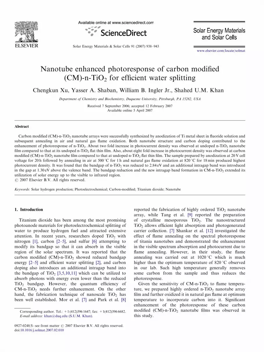
nanotube array annealed in various conditions. It showsthat the CM-n-TiO2 nanotube array consists of rutile phaseregardless of the annealing conditions since the flameoxidation temperature of 820 1C is well above thetemperature for rutile TiO2 formation.Fig. 5 shows the SEM top image of (CM)-n-TiO2
nanotube array prepared by anodization at 20V cellvoltage for 20 h followed by annealing in air at 500 1Cfor 1 h and natural gas flame oxidation at 820 1C for18min. The average diameter of the nanotubes was foundto be of the order of 100 nm, with the wall thickness ofabout 20 nm. It was noted that the nanotube array haspartially collapsed due to the high temperature treatmentat 820 1C. [13]The UV–Vis spectra of the samples are shown in Fig. 6.
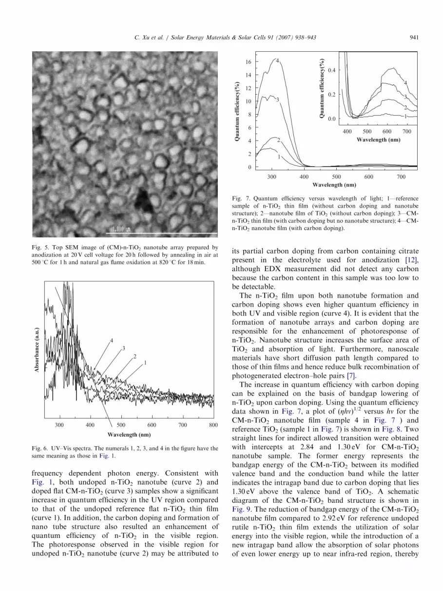
Carbon doped samples (3 and 4) show absorption in theUV to visible region. The undoped flat TiO2 film (curve 1)did not show any absorption in the visible region.Fig. 7 shows the quantum efficiency versus wavelength
for the four samples shown in Fig. 1. Note that thequantum efficiency Z was calculated using Z ¼ jP(l)hn/eI0(l), where jP(l) is wavelength dependent photocurrentdensity, e is the electronic charge, I0(l) is wavelengthdependent intensity of incident light, and hn represents
ARTICLE IN PRESS
Fig. 5. Top SEM image of (CM)-n-TiO2 nanotube array prepared by
anodization at 20V cell voltage for 20 h followed by annealing in air at
500 1C for 1 h and natural gas flame oxidation at 820 1C for 18min.
300 400 500 600 700 800
Wavelength (nm)
Ab
sorb
an
ce (
a.u
.)
4
3
21
Fig. 6. UV–Vis spectra. The numerals 1, 2, 3, and 4 in the figure have the
same meaning as those in Fig. 1.
300 400 500 600 700
0
2
4
6
8
10
12
14
16
400 500 600 700
0.0
0.2
0.4
Qu
an
tum
eff
icie
ncy
(%)
4
3
2
1
Wavelength (nm)
4
3
2
1
Qu
an
tum
eff
icie
ncy
(%)
Wavelength (nm)
Fig. 7. Quantum efficiency versus wavelength of light; 1—reference
sample of n-TiO2 thin film (without carbon doping and nanotube
structure); 2—nanotube film of TiO2 (without carbon doping); 3—CM-
n-TiO2 thin film (with carbon doping but no nanotube structure); 4—CM-
n-TiO2 nanotube film (with carbon doping).
C. Xu et al. / Solar Energy Materials & Solar Cells 91 (2007) 938–943 941
frequency dependent photon energy. Consistent withFig. 1, both undoped n-TiO2 nanotube (curve 2) anddoped flat CM-n-TiO2 (curve 3) samples show a significantincrease in quantum efficiency in the UV region comparedto that of the undoped reference flat n-TiO2 thin film(curve 1). In addition, the carbon doping and formation ofnano tube structure also resulted an enhancement ofquantum efficiency of n-TiO2 in the visible region.The photoresponse observed in the visible region forundoped n-TiO2 nanotube (curve 2) may be attributed to
its partial carbon doping from carbon containing citratepresent in the electrolyte used for anodization [12],although EDX measurement did not detect any carbonbecause the carbon content in this sample was too low tobe detectable.The n-TiO2 film upon both nanotube formation and
carbon doping shows even higher quantum efficiency inboth UV and visible region (curve 4). It is evident that theformation of nanotube arrays and carbon doping areresponsible for the enhancement of photoresponse ofn-TiO2. Nanotube structure increases the surface area ofTiO2 and absorption of light. Furthermore, nanoscalematerials have short diffusion path length compared tothose of thin films and hence reduce bulk recombination ofphotogenerated electron–hole pairs [7].The increase in quantum efficiency with carbon doping
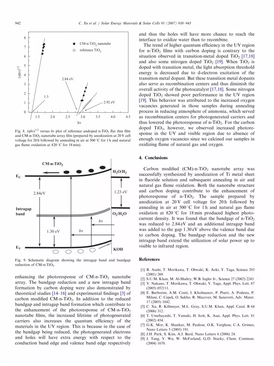
can be explained on the basis of bandgap lowering ofn-TiO2 upon carbon doping. Using the quantum efficiencydata shown in Fig. 7, a plot of (Zhn)1/2 versus hn for theCM-n-TiO2 nanotube film (sample 4 in Fig. 7 ) andreference TiO2 (sample 1 in Fig. 7) is shown in Fig. 8. Twostraight lines for indirect allowed transition were obtainedwith intercepts at 2.84 and 1.30 eV for CM-n-TiO2
nanotube sample. The former energy represents thebandgap energy of the CM-n-TiO2 between its modifiedvalence band and the conduction band while the latterindicates the intragap band due to carbon doping that lies1.30 eV above the valence band of TiO2. A schematicdiagram of the CM-n-TiO2 band structure is shown inFig. 9. The reduction of bandgap energy of the CM-n-TiO2
nanotube film compared to 2.92 eV for reference undopedrutile n-TiO2 thin film extends the utilization of solarenergy into the visible region, while the introduction of anew intragap band allow the absorption of solar photonsof even lower energy up to near infra-red region, thereby
ARTICLE IN PRESS
1.5 2.0 2.5 3.0 3.5 4.0 4.5
0
1
2
3
4
5
6
7
8
CM-n-TiO2 nanotube
reference TiO2
2.84 eV
1.3
2.92 eV
(ηhν
)1/2
hν
Fig. 8. (Zhn)1/2 versus hn plot of reference undoped n-TiO2 flat thin film
and CM-n-TiO2 nanotube array film (prepared by anodization at 20V cell
voltage for 20 h followed by annealing in air at 500 1C for 1 h and natural
gas flame oxidation at 820 1C for 18min).
H2O/H2
O2/H2O
1.23 eV2.84eV
1.30 eV
EC
EV
Intragap
band
hν
hν
CM-n-TiO2
KOH
Fig. 9. Schematic diagram showing the intragap band and bandgap
reduction of CM-n-TiO2.
C. Xu et al. / Solar Energy Materials & Solar Cells 91 (2007) 938–943942
enhancing the photoresponse of CM-n-TiO2 nanotubearray. The bandgap reduction and a new intragap bandformation by carbon doping were also demonstrated bytheoretical studies [14–16] and experimental findings [3] ofcarbon modified CM-n-TiO2. In addition to the reducedbandgap and intragap band formation which contribute tothe enhancement of the photoresponse of CM-n-TiO2
nanotube films, the increased lifetime of photogeneratedcarriers also increases the quantum efficiency of thematerials in the UV region. This is because in the case ofthe bandgap being reduced, the photogenerated electronsand holes will have extra energy with respect to theconduction band edge and valence band edge respectively
and thus the holes will have more chance to reach theinterface to oxidize water than to recombine.The trend of higher quantum efficiency in the UV region
for n-TiO2 films with carbon doping is contrary to thesituation observed in transition-metal doped TiO2 [17,18]and also some nitrogen doped TiO2 [19]. When TiO2 isdoped with transition metal, the light absorption thresholdenergy is decreased due to d-electron excitation of thetransition metal dopant. But these transition metal dopantsalso serve as recombination centers and thus diminish theoverall activity of the photocatalyst [17,18]. Some nitrogendoped TiO2 showed poor performance in the UV region[19]. This behavior was attributed to the increased oxygenvacancies generated in those samples during annealingprocess in reducing atmosphere of ammonia, which servedas recombination centers for photogenerated carriers andthus lowered the photoresponse of n-TiO2. For the carbondoped TiO2, however, we observed increased photore-sponse in the UV and visible region due to absence ofenough oxygen vacancies since we calcined our samples inoxidizing flame of natural gas and oxygen.
4. Conclusions
Carbon modified (CM)-n-TiO2 nanotube array wassuccessfully synthesized by anodization of Ti metal sheetin fluoride solution and subsequent annealing in air andnatural gas flame oxidation. Both the nanotube structureand carbon doping contribute to the enhancement ofphotoresponse of n-TiO2. The sample prepared byanodization at 20V cell voltage for 20 h followed byannealing in air at 500 1C for 1 h and natural gas flameoxidation at 820 1C for 18min produced highest photo-current density. It was found that the bandgap of n-TiO2
was reduced to 2.84 eV and an additional intragap bandwas added to the gap 1.30 eV above the valence band dueto carbon doping. The bandgap reduction and the newintragap band extend the utilization of solar power up tovisible to infrared region.
References
[1] R. Asahi, T. Morikawa, T. Ohwaki, K. Aoki, Y. Taga, Science 293
(2001) 269.
[2] S.U.M. Khan, M. Al-Shahry, W.B. Ingler Jr., Science 27 (2002) 2243.
[3] Y. Nakano, T. Morikawa, T. Ohwaki, Y. Taga, Appl. Phys. Lett. 87
(2005) 052111.
[4] E. Barborini, A.M. Conti, I. Kholmanov, P. Piseri, A. Podesta, P.
Milani, C. Cepek, O. Sakho, R. Macovez, M. Sancrotti, Adv. Mater.
17 (2005) 1842.
[5] C. Xu, R. Killmeyer, M.L. Gray, S.U.M. Khan, Appl. Catal. B 64
(2006) 312.
[6] T. Umebayashi, T. Yamaki, H. Itoh, K. Asai, Appl. Phys. Lett. 81
(2002) 454.
[7] G.K. Mor, K. Shankar, M. Paulose, O.K. Varghese, C.A. Grimes,
Nano Letters 5 (2005) 191.
[8] J.H. Park, S. Kim, A.J. Bard, Nano Letters 6 (2006) 24.
[9] J. Tang, Y. Wu, W. McFarland, G.D. Stucky, Chem. Commun.
(2004) 1670.

ARTICLE IN PRESSC. Xu et al. / Solar Energy Materials & Solar Cells 91 (2007) 938–943 943
[10] C. Xu, R. Killmeyer, M.L. Gray, S.U.M. Khan, Electrochem.
Commun. 8 (2006) 1650.
[11] C. Xu, S.U.M. Khan, Electrochem. Solid St. 10 (2007) B56.
[12] K. Shankar, M. Paulose, G.K. Mor, O.K. Varghese, C.A. Grimes, J.
Phys. D 38 (2005) 3543.
[13] O.K. Varghese, D. Gong, M. Paulose, Craig.A. Grimes, E.C. Dickey,
J. Mater. Res. 18 (2003) 156.
[14] C.D. Valentin, G. Pacchioni, A. Selloni, Chem. Mater. 17 (2005) 6656.
[15] H. Wang, J.P. Lewis, J. Phys.: Condens. Matter 17 (2005) L209.
[16] X. Nie, K. Sohlberg, Mat. Res. Soc. Symp. Proc. 801 (2004) B205.
[17] S.T. Martin, C.L. Morrison, M.R. Hoffmann, J. Phys. Chem. 98
(1994) 13695.
[18] W. Choi, A. Termin, M.R. Hoffmann, J. Phys. Chem. 98 (1994)
13669.
[19] H. Irie, Y. Watanabe, K. Hashimoto, J. Phys. Chem. B 107 (2003)
5483.