nanotube-based nanoelectromechanical systems
TRANSCRIPT

ISSN 1063-7761, Journal of Experimental and Theoretical Physics, 2006, Vol. 103, No. 3, pp. 449–462. © Pleiades Publishing, Inc., 2006.Original Russian Text © Yu.E. Lozovik, A.G. Nikolaev, A.M. Popov, 2006, published in Zhurnal Éksperimental’no
œ
i Teoretichesko
œ
Fiziki, 2006, Vol. 130, No. 3, pp. 516–533.
449
1. INTRODUCTION
Considerable progress has been made in nanome-chanics over the past decade. For example, it wasshown that nanoscale objects can be manipulated [1],and schemes of nanoelectromechanical systems(NEMS) that can be used to control nanoscale motionwere considered in [2]. Search for nanoscale objectsthat can be used as moving parts in NEMS devicesremains a challenging problem. Observations of spon-taneous [3, 4] and controlled [5] relative motion of car-bon nanotube walls [6–8] and their unusual elasticproperties [9–12] suggest that they are promising can-didates to be used as moving parts of NEMS devices. Anumber of nanomechanical devices based on interlayersliding or relative rotation of nanotube walls have beenproposed: electrically driven nanobearing [13] and nan-ogear [14], a nanospring [5], a nanoswitch [15], and agigahertz oscillator [16]. The unique electronic pro-perties of carbon nanotubes [17] are used in experimen-tal nanoscale electronic devices, such as nanotransis-tors [18], nanodiodes [19], random access memorycells [20], current modulators [21], etc. A variable nanore-sistor that utilizes both mechanical and electronic proper-ties of nanotubes was proposed in [22–24]. Moreover,relative rotation of carbon nanotube walls was imple-mented in recently constructed nanomotors [25, 26]. Inthe nanoresistor and nanomotor mentioned above, nan-otube walls play the roles of both moving parts andelectric circuit elements. Recently, a new unique possi-bility of using carbon nanotubes in NEMS was demon-strated: it was shown that the structure of a double-walled nanotube can be similar to that of a threadedassembly [27].
In this paper, we consider various operation modesof NEMS devices containing a double-walled nanotube
with chiral potential energy surface of interwall interac-tion, which can be called
bolt–nut pair.
We determineconditions for different modes of operation and discussboth their feasibility in various NEMS devices andmethods of application of driving forces for varioustypes of motion. We develop a model for computing theinterwall interaction energy in nanotubes with atomicstructural defects. Our computations of the interwallinteraction energy show that periodic distribution ofatomic defects in a double-walled nanotube can createconditions required for synthesizing nanotubes that canbe used as bolt–nut pairs with desired thread character-istics. We discuss the feasibility of fabrication of nano-tubes of this type by self-organization. We proposenovel schemes of carbon-nanotube–based NEMSdevices containing such a bolt–nut pair: a nanodrill thatcan be used to modify surfaces (see also [22–24]) and ananomotor in which the force directed along the nano-tube axis is converted into relative rotation of its walls.
We also note that the double-walled nanotubes ana-lyzed theoretically in this paper can be synthesized bythe standard arc discharge method [28], by the hydro-gen arc discharge method [29], by catalytic decomposi-tion of hydrocarbons [30, 31], and by heating [32] orelectron beam lithography [33] applied to single-wallednanotubes containing chains of fullerene molecules.
The paper is organized as follows. In Section 2, weanalyze the symmetry of the interwall interactionpotential surface in double-walled nanotubes with andwithout atomic structural defects. In Section 3, wedescribe a model for computing the interwall interac-tion energy in double-walled nanotubes with defects.Section 4 presents computed characteristics of nano-tubes as bolt–nut pairs. In Section 5, we proposeschemes of NEMS devices containing a nanotube-based bolt–nut pair and discuss control of motion and
Nanotube-Based Nanoelectromechanical Systems
Yu. E. Lozovik, A. G. Nikolaev, and A. M. Popov
Institute of Spectroscopy, Russian Academy of Sciences, Troitsk, Moscow oblast, 142190 Russiae-mail: [email protected]; [email protected]
Received April 20, 2006
Abstract
—Nanoelectromechanical systems based on multiwalled carbon nanotubes are considered. Control ofmotion and modes of operation of these systems are discussed. The structure of double-walled carbon nano-tubes with atomic structural defects that can be used as bolt–nut pairs is analyzed. Energy barriers and thresholdforces for relative motion of walls along and across the “thread” are computed for double-walled nanotubeswith various types of defects. It is found that the qualitative characteristics of the thread are independent of thetype of defect. Feasibility of fabricating double-walled nanotubes for use as bolt–nut pairs by self-organizationis discussed.
PACS numbers: 61.46.Fg, 85.85.+j, 87.80.Mj
DOI:
10.1134/S1063776106090159
ELECTRONIC PROPERTIES OF SOLIDS
450
JOURNAL OF EXPERIMENTAL AND THEORETICAL PHYSICS
Vol. 103
No. 3
2006
LOZOVIK et al.
modes of operation of these systems. Our conclusionsare presented in Section 6.
2. POTENTIAL ENERGY SURFACES OF DOUBLE-WALLED NANOTUBES
WITH COMMENSURATE WALLS
To examine the characteristics of relative motion ofnanotube walls, the interwall interaction energy
U
mustbe calculated as a function of the coordinates describ-ing the relative position of the walls, the angle
φ
of theirrelative rotation about the nanotube axis and the rela-tive displacement
z
along the axis. The potential energysurface
U
(
φ
,
z
) is conveniently visualized as a contourplot on a developed cylindrical surface. In principle, adouble-walled nanotube can be used as a bolt–nut pairwhen the potential energy surface has helical valleysanalogous to a bolt thread. Hereinafter, reliefs of thistype are referred to as threadlike. Their quantitativecharacteristics are the energy barriers
E
1
and
E
2
for rel-ative motion of nanotube walls along and across thethread (“thread stripping”), respectively, and the corre-sponding threshold (static frictional) forces. As a qual-itative characteristic of the thread, we can use the ratio
β
=
E
2
/
E
1
called
relative depth of thread
[22, 23].
Since a nanotube has chiral walls in the general case[34], most nanotubes have threadlike potential reliefs.However, the thread characteristics of threadlike nano-tubes without wall defects are incompatible with theiruse as bolt–nut pairs in NEMS devices (see below).Since a nanotube wall is a quasi-one-dimensional crys-tal [17, 35], a double-walled nanotube can be eithercommensurate or incommensurate [36]. Originally,threadlike potential reliefs were found for incommensu-rate nanotubes, with the length of one wall assumed to beequal to the unit cell size (normally, several nanometersor tens of nanometers) to simplify analysis [27]. How-ever, a detailed analysis showed that the depth of threadand, therefore, the thread-stripping force is small forany wall length [22, 23]. Moreover, the depth of athread strongly fluctuates with the length of the shortmoving wall, and the energy surface may even be flatfor certain values of the wall length [22, 23]. Therefore,it is hardly possible to synthesize an incommensuratenanotube that can be used as a bolt–nut pair with thedesired depth of thread. Nanotubes with commensurateachiral walls cannot have threadlike potential reliefs[37, 38]. When a commensurate nanotube has at leastone chiral wall, the walls have incompatible symme-tries [36–40], and all energy barriers for relative motionof walls are very low, because only high-order Fouriercomponents of the interaction potential
U
a
between anatom in one layer and the entire other layer contributeto the barriers [39].
It turns out that nanotubes with atomic structuraldefects have totally different characteristics. In par-ticular, even the first Fourier component of
U
a
contrib-utes to barriers. The resulting barriers are higher by
8
−
10 orders of magnitude (see below). This property ofdouble-walled nanotubes with atomic structural defectsmakes it possible to synthesize nanotubes with thread-like reliefs that can be used as bolt–nut pairs in NEMSdevices. It was proposed to create identical defects atsimilar locations in many unit cells of double-wallednanotubes with commensurate walls [38, 41]. (We dis-cuss the feasibility of creating such defects by self-organization in Section 5.) For a nanotube of this kind,any barrier
∆
U
for relative motion of walls can beexpressed as
where
∆
U
u
is the barrier per unit cell and
N
u
is the num-ber of cells containing defects. Thus, “atomic-scaledesign” of double-walled nanotube structure makes itpossible to fabricate bolt–nut pairs by synthesizinglong nanotubes with barriers sufficiently high to pre-vent thread stripping.
To date, numerous experimental [42–45] and theo-retical [46–53] studies of doped carbon nanotubes withatomic structural defects have been conducted. Defectsof various types have been considered: point and dou-ble vacancies [46]; pentagon–heptagon pairs [46];Stone–Wales defects [47]; substitutional doping withboron [42–44, 48, 49], nitrogen [42, 48–50], andsilicon [51]; and adsorption on the outer wall surface[45, 52, 53].
As mentioned above, computations show that inter-layer corrugations of the potential relief
U
(
φ
,
z
) for dou-ble-walled nanotubes with chiral commensurate wallsare too small for using nanotubes of this kind in NEMSdevices, in particular, in bolt–nut pairs. Moreover, weshow here that a typical commensurate nanotube can-not have a threadlike relief
U
(
φ
,
z
). To do this, we con-sider the Fourier expansion of potential energy
(1)
where
b
is the unit cell size, and
M
and
K
are integers,following the approach developed in [37, 39, 54].
If the energy
U
i
of interaction between two objectsis a function of the coordinates describing their relativeposition only, then the symmetry group of
U
i
is thedirect product of the symmetries of the interactingobjects. Therefore, expansion (1) contains only the har-monics compatible with the symmetries of both nano-tube walls.
Exhaustive presentations of the selection rules foradmissible harmonics can be found in [37, 39, 54]. Thenumbers
M
of the harmonics compatible with the rota-
∆U ∆UuNu,=
U φ z,( ) αKM 2π
b------Kz Mφ+⎝ ⎠
⎛ ⎞cosM K, 0=
∞
∑=
+ βK 'M ' 2π
b------K 'z M 'φ–⎝ ⎠
⎛ ⎞ ,cosM ' K ', 0=
∞
∑

JOURNAL OF EXPERIMENTAL AND THEORETICAL PHYSICS
Vol. 103
No. 3
2006
NANOTUBE-BASED NANOELECTROMECHANICAL SYSTEMS 451
tional symmetries of the walls are determined by theselection rules
(2)
where
n
1
and
n
2
are the orders of the principal rotationaxes of the inner and outer walls, respectively. Thenumbers
K
of the harmonics compatible with the trans-lational symmetries of the walls are determined by theselection rules
(3)
where
b
1
and
b
2
are the unit cell sizes in the inner andouter walls, respectively. Invariance of
U
(
φ
,
z
) under
the respective helical symmetry groups and ofthe inner and outer walls entails the selection rules
(4)
(5)
where
j
1
, ,
j
2
, and are integers; the parameters
q
1
,
r
1
and
q
2
,
r
2
are determined by the chiral indices of thelayers [54]. Note that the pairs (
M
,
K
) and (
M
',
K
') areselected by independent systems of equations.
Recently, a classification was proposed for com-mensurate double-walled nanotubes [38, 55], based onthe concept of equivalence class defined as the totalityof walls with chiral indices (
n
'
f
,
n
'
g
), where
n
' is theorder of the principal rotation axis, and
f
and
g
arecoprime numbers called commensurability indices. Itwas shown that all walls in each particular equivalenceclass are characterized by equal values of unit cell size,parameter
r
, and the number
A
=
q
/
n
' of graphene unitcells within the sector of angle 2π/n' in the unit cell ofthe wall [38]:
(6)
where R = 3 if (f – g)/3 is an integer and R = 1 otherwise.According to this classification, the double-walled
nanotubes with inner and outer walls in the same equiv-alence class constitute a family in which both interwalldistance and the difference ∆n = n2 – n1 are constant.
By virtue of (6), when inner and outer walls belongto the same equivalence class (as in (5,5)@(10,10) or
M M1n1 M2n2, M ' M1' n1 M2' n2,= = = =
b/K b1/K1 b2/K2,= =
b/K ' b1/K1' b2/K2' ,= =
Tq1
r1 Tq2
r2
M1r1 K1+ q1/n1( ) j1,=
M1' r1 K1'– q1/n1( ) j1' ,=
M2r2 K2+ q2/n2( ) j2,=
M2' r2 K2'– q2/n2( ) j2' ,=
j1' j2'
b1 b2 b, r1 r2 r,= = = =
Aq1
n1-----
q2
n2-----
2 f 2 fg g2+ +( )R
-------------------------------------,= = =
(8,2)@(16,4) tubes), Eqs. (3)–(5) reduce to
(7)
(8)
(9)
We solved the system of Eqs. (2), (7)–(9) for allfamilies of double-walled nanotubes with walls in thesame equivalence class (listed in [38]) to find theadmissible pairs (M, K) in (1) (compatible with the wallsymmetries) in expansion (1). If n1/n or n2/n is an evennumber (n is the lowest common denominator of n1 andn2), then
(10)
where k and l are nonnegative integers. If both n1/n andn2/n are odd, then we have two sets of pairs compatiblewith the symmetries of both walls, which are given,respectively, by (10) and the expression
(11)
where k' and l' are nonnegative integers. The pairs(M', K') are determined by expressions similar to (10)and (11). Note that this result generalizes that obtainedin [54] for nanotubes with commensurate achiral walls.
Calculations show that the Fourier amplitudes of thepotential rapidly decrease with increasing harmonicnumber [37, 39]. Accordingly, the potential energyrelief U(φ, z) is determined by the largest amplitudes,which correspond to the lowest numbers (Ms, Ks). Inparticular, when the largest amplitude corresponds toKs = 0, the valleys of the potential are circumferentialstrips on the cylindrical surface (φ, z). When the largestamplitude corresponds to Ms = 0, the valleys are longi-tudinal strips. Only when the largest amplitude corre-sponds to nonzero Ms and Ks, the valleys are helicalstrips and the potential relief is threadlike.
It is obvious that the lowest harmonic numbersgiven by (10) are (Ms, 0) and (0, Ks). The correspondingnanotubes cannot have threadlike potential reliefs.(Note that both walls of such a nanotube are chiral.)The set of harmonic numbers given by (11) does notcontain zero. The corresponding set of nanotubes mayinclude those with threadlike potential reliefs, but theyare not uniquely determined by the symmetries of thewalls. In addition, the Fourier amplitude correspondingto the lowest numbers (Ms/2, Ks/2) given by (11) mustbe larger than the amplitude corresponding to the low-est numbers (Ms , 0) and (0, Ks) given by (10).
K K1 K2, K ' K1' K2' ,= = = =
M1r1 K1+ A j1, M1' r1 K1'– A j1' ,= =
M2r2 K2+ A j2, M2' r2 K2'– A j2' .= =
M K,( ) AlAn1n2k
2n------------------,⎝ ⎠
⎛ ⎞ ,=
M K,( ) A 2l ' 1+( )2
------------------------An1n2 2k ' 1+( )
2n------------------------------------,⎝ ⎠
⎛ ⎞ ,=
452
JOURNAL OF EXPERIMENTAL AND THEORETICAL PHYSICS Vol. 103 No. 3 2006
LOZOVIK et al.
Since the harmonic numbers given by (11) corre-spond to nanotubes for which both n1/n and n2/n are odd(see above), the difference ∆n = n2 – n1 is an even num-ber. Using the list of all families of double-walled nan-otubes with commensurate walls in the same equiva-lence class [38], we find that threadlike potential reliefsare possible only for nanotubes from three families:
(2l, l)@(2l + 8, l + 4),
(3l, 2l)@(3l + 6, 2l + 4),
(4l, l)@(4l + 8, l + 2),
where l is an integer. In these families, the lowest har-monic numbers (Ms/2, Ks/2) correspond to the nano-tubes with the smallest admissible ratios n1/n and n2/n.Finally, we obtain
(6, 3)@(14, 7), (3, 2)@(9, 6), (4, 1)@(12, 3).
The corresponding pairs (Ms/2, Ks/2) are (7, 105),(19, 57), and (7, 21), respectively. The Fourier compo-nents with these high harmonic numbers are extremelyweak [37, 39]. Therefore, even if the amplitude of sucha component is larger than those with the numbers(Ms, 0) and (0, Ks), the thread-stripping barrier is toolow, and the corresponding nanotube cannot be used asa bolt–nut pair in NEMS devices. For nanotubes withwalls from different equivalence classes, the harmonicnumbers compatible with the symmetries of both wallsare even higher, and the barriers for relative motion ofany type are even lower. For this reason, we considerthe creation of defects at similar locations in the unitcells (by self-organization) [24, 38] as an alternativeapproach to synthesis of bolt–nut pairs.
Since an achiral wall has mirror symmetry planescontaining the principal rotation axis, the Fourieramplitudes corresponding to left- and right-hand
threads are equal: = for M = M' and K = K'. Thecorresponding nanotubes cannot have threadlike poten-tial reliefs [37, 38]. This conclusion holds when onewall is achiral and the other has atomic structuraldefects. Thus, a double-walled nanotube with periodi-cally located atomic structural defects of the type con-sidered in this paper can be used as a bolt–nut pair onlyif the corresponding defect-free nanotube is chiral.
3. CALCULATION OF INTERWALL INTERACTION
To date, neither interwall interaction in a carbonnanotube nor even interaction between graphene sheetshas been studied in detail. For example, both measuredand calculated values of interlayer interaction energyfor graphite differ by two orders of magnitude (see [56]and references therein). The threshold forces for rela-tive motion along the nanotube axis were measuredonly in a few experiments [3–5]. In theoretical studies,
αKM βK '
M '
only barriers for relative motion of walls in(5,5)@(10,10) double-walled nanotubes were deter-mined by invoking ab initio methods [27, 37, 38]. Dif-ferent computational methods lead to different valuesof the barriers Ez and Eφ for relative sliding and rotationof walls, respectively. However, similar ratios βb =Eφ/Ez were predicted for a particular nanotube by differ-ent methods: βb = 2.26 [57], 2.08 [40], and 2.85 [58]were obtained by using density functional theory; βb =3.5 was obtained by the tight-binding method [59]; andβb = 3.1 and 2.9 were obtained when the interlayerinteraction was modeled by using the Lennard-Jonespotential
with 0 = 2.968 meV and σ0 = 3.407 Å and com-putations were performed for walls with annealedstructure [27] and rigid walls [38], respectively. More-over, the use of the Lennard-Jones [38], as well as othersemiempirical potentials [36, 37], made it possible toobtain the following qualitative result: all potentialenergy surfaces computed for commensurate double-wall nanotubes with at least one chiral wall are almostflat. This suggests that the simple Lennard-Jones poten-tial can be used to adequately predict qualitative char-acteristics of potential reliefs. Furthermore, the numberof atoms per unit cell in commensurate chiral nano-tubes is too large for interlayer interaction to be amena-ble to ab initio simulation.
The discussion presented above provides sufficientreason for using the Lennard-Jones potential as an ade-quate approximation for studying qualitative character-istics of relative motion of walls in double-walled car-bon nanotubes. In this study, we use the Lennard-Jonespotential with parameter values given above to describeinteraction between atoms belonging to neighboringwalls. Note that the Lennard-Jones potential has beensuccessfully used to analyze the ground state and phasetransitions in a C60 crystal [60], to investigate the inter-wall interaction energy surface relief [22–24, 27, 38, 61],and to calculate characteristics of nanotubes as giga-hertz oscillators [16, 62–67]. To eliminate the effect ofnanotube edges on the potential relief, we considertubes with long inner and short outer walls. We set theouter wall length equal to the unit cell size and take aninner wall length such that all atom pairs with inter-atomic distances smaller than the cutoff distance 40σ0of the potential are taken into account. We note thatwall deformation does not significantly change thecharacteristics of the potential reliefs of both double-walled nanotubes [36, 38] and bilayer nanoparticles[68, 69]. For example, the barriers for relative rotationand sliding of walls in (5,5)@(10,10) nanotubes com-puted without annealing the wall structure [38] differonly by 14% from those obtained for walls withannealed structure in [27]. For this reason, we consider
U 40
σ0
r-----⎝ ⎠
⎛ ⎞12 σ0
r-----⎝ ⎠
⎛ ⎞6
–=
JOURNAL OF EXPERIMENTAL AND THEORETICAL PHYSICS Vol. 103 No. 3 2006
NANOTUBE-BASED NANOELECTROMECHANICAL SYSTEMS 453
interaction between rigid walls in double-walled nano-tubes. Wall structure can be determined by rolling agraphene sheet with a bond length of 1.42 Å (the bondlength in multiwalled nanotubes is equal to that ingraphene within an error of neutron diffraction mea-surements of about 0.01 Å [70]).
For any double-walled nanotube with commensu-rate chiral walls, the potential surface computed byusing a semiempirical potential is almost flat. Aspointed out in Section 2, this is explained by the factthat the walls have incompatible symmetries [39]. Inparticular, the barrier for relative rotation of walls in a(8,2)@(16,4) nanotube computed by using the Len-nard-Jones potential (about 5 × 10–12 meV per atom),and this is the only example where the computed barrierfor relative motion of walls in a commensurate chiralnanotube exceeds the numerical error [38]. In computa-tions using the potential introduced by Kolmogorovand Crespi [36], very smooth potentials were alsoobtained for all defect-free nanotubes with commensu-rate chiral walls [37]. The energy Udef of interwall inter-action in double-walled nanotubes containing defectscan be written as
(12)
where Uperf is the interwall interaction energy fordefect-free nanotubes; Np is the number of atoms in adefect-free wall; Nd is the number of atoms in a wallwhose positions or properties change in the presence ofdefects; and (φ, z), (φ, z) are the energies ofinteratomic interaction for a defect-free wall andbetween the Nd atoms with modified properties in nan-otubes with and without defects, respectively. Since thepotential surface of a defect-free commensurate chiralnanotube is almost flat (Uperf(z, φ) ≈ U0, where U0 isconstant), the first term in (12) does not contribute tothe potential relief and, therefore, to the barriers for rel-ative motion of walls. Accordingly, we can take intoaccount only the interactions between the Nd atomswhose characteristics are modified by defects. Thus, thenumerical complexity of potential-surface computa-tions can be substantially reduced for commensuratechiral nanotubes containing defects. Note that this can-not be done when both walls are achiral, because poten-tial surfaces with substantial barriers for relativemotion have been revealed for such nanotubes even inthe case of perfect walls [38–40, 58].
In this paper, we consider two types of defects: apoint defect and a substitutional atom characterized bymodified parameters of interaction with carbon atomsin the other wall. The latter may be the atom of a differ-ent element or a carbon atom with electronic propertiesmodified by chemical adsorption of atoms or mole-
Udef φ z,( ) Uperf φ z,( )=
+ Ui jdefφ z,( ) Uijperf
φ z,( )–( )[ ],i j, 1=
i Np j, Nd= =
∑
UijdefUijperf
cules. Currently, no experimental data are available thatcan be used for parameter fitting in the potential ofinteraction between an atom with properties modifiedby a defect and a carbon atom in the other wall. For thisreason, we use the Lennard-Jones potential
with parameters 1 and σ1 different from those in thepotential that describes interactions between carbonatoms: 1 = α0 and σ1 = γσ0. Since all defects consid-ered in this study modify the interaction parameters foronly one carbon atom (i.e., Nd = 1), we call them single-atom defects. It is clear from Eq. (12) that the barriersfor relative motion of walls of any kind scale with α.Therefore, the relative depth β of thread is independentof α.
4. COMPUTATION OF EFFECTIVE THREAD CHARACTERISTICS
FOR A DOUBLE-WALLED NANOTUBE
All potential energy surfaces computed in this study,as well as barriers and threshold forces for relativemotion of walls, correspond to the case when the innerwall is much longer than the outer one and the outerwall position is in the middle of the inner one. Thus, weneglect the effect of nanotube edges on the interwallinteraction. The outer wall length is set equal to100 nm.
Figure 1 illustrates the potential reliefs correspond-ing to several types of thread in a commensurate chiralnanotube with a single vacancy and a single defect perunit cell. The minima of potential energy make up a lat-tice with primitive vectors a and b. It is obvious that itsparameters are related to those of the correspondingdefect-free lattice [22]. To examine this relationship inmore detail, we change from the angular coordinate φto the coordinate L = φR1 defined as the arc lengthswept by the angle of rotation an atom moving with thewall and R1 is the radius of the defect-free wall. In thecoordinate system (L, z), the vectors a and b have mag-nitudes of a = b = a0, where a0 = 2.46 Å is the magni-tude of the graphene lattice vector, and make an angleof 60°. For nanotubes with incommensurate walls, wefound two types of lattice made by the potential energyminima, a square lattice (type I) and triangular lattice(type II) [22]. All helical potential reliefs obtained inthis study have type II lattices.
Let us discuss the geometric thread characteristics.In the coordinate system introduced above, the threadangle χ (the angle between the thread direction and thetube circumference) can be represented as
(13)
where θ is the chiral angle for the defect-free wall and
U 41
σ1
r-----⎝ ⎠
⎛ ⎞12 σ1
r-----⎝ ⎠
⎛ ⎞6
–=
χ θ k 60°,⋅+=

454
JOURNAL OF EXPERIMENTAL AND THEORETICAL PHYSICS Vol. 103 No. 3 2006
LOZOVIK et al.
k is 0, 1, or 2. Figure 2 shows possible thread directionsin the development of the wall. The chiral angle θ of ananotube wall can be expressed as follows [17, 35]:
(14)
where m1 and m2 are the chiral indices of the wall. It isobvious that the number Nt of threads equals the orderof the principal rotation axis of the defect-free wall(m is the greatest common divisor of m1 and m2). Table 1shows the values of chiral angle θ of the defect-freewall, thread angle χ, number Nt of threads, and pitch hfor the nanotubes considered in this study. The pitch isdefined here as
(15)
Figures 1b and 1c show, respectively, the potentialenergy surfaces for the small and large values of theparameter γ (γ = 0.8 and 1.5) in the potential of interac-tion between the substitutional atom and an atom in theother wall. The interaction between the substitutionalatom and the nearest-neighbor atom in the other wallcorresponds to the attractive and repulsive portions ofthe potential when γ is small and large, respectively.Accordingly, we consider attractive and repulsivepotential reliefs, Ua and Ur. Note that the correspondingpotential reliefs depicted in Fig. 1 look like comple-mentary positive and negative images, and their 3Dplots are the complementary casts of one another. To
θ2m1 m2+
2 m12 m2
2 m1m2+ +----------------------------------------------,arccos–=
h 2πR1 χ.sin=
quantify this property of the attractive and repulsivepotential reliefs, we rescale the corrugations of Ua tomatch the corrugations of Ur:
(16)
The scaling factor is defined as A = ∆Ur/∆Ua, wherecorrugation scales ∆Ua and ∆Ur denote the differencesbetween the maxima and minima of the attractive andrepulsive reliefs, respectively. The overall relief
(17)
characterizes the difference between the shapes of the
Ua' z φ,( ) A Ua z φ,( ) Ua z φ,( )⟨ ⟩ z φ,–[ ].=
S z φ,( ) Ua' z φ,( ) Ur z φ,( )+=
(c)(b)(‡)
6
4
2
0
z
30 60 90
6
4
2
0
z
30 60 90
6
4
2
0
z
30 60 90ϕ, deg
b
‡
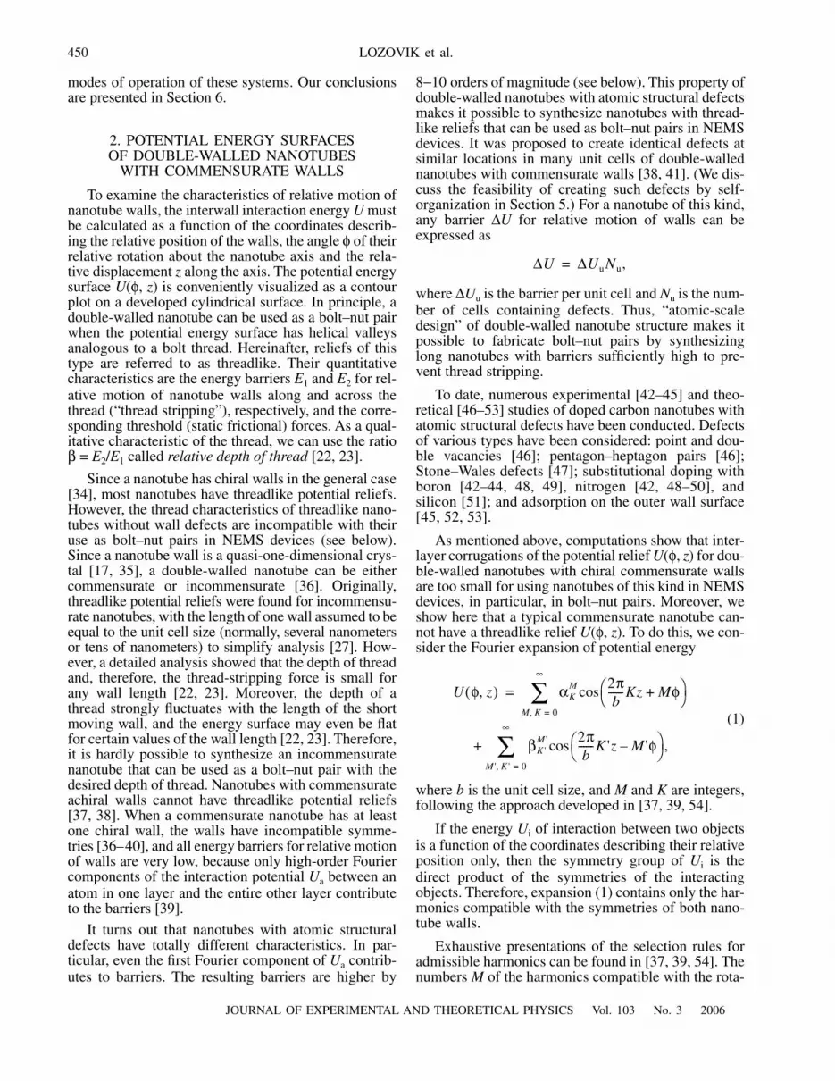
Fig. 1. Potential energy surface of interwall interaction for (4,6)@(12,8) double-walled nanotube as a function of relative axial dis-placement z and angle φ of relative rotation about the axis: (a) one vacancy per unit cell of the inner wall; (b), (c) one substitutionalatom per unit cell of the outer wall. Parameters of interaction between the substitutional atom and atoms in the defect-free wall:(b) α = 2.0, γ = 0.8; (c) α = 2.0, γ = 1.5. Energy is measured from its minimum. Equipotential curves are drawn with steps(a) 10 meV, (b) 33 meV, and (c) 12 eV; a and b are the primitive vectors of the lattice made by the minima of the potential relief.
d c θ
Fig. 2. Wall unit cell developed on a graphene sheet isshown as a rectangle with sides c and d. The lengths of c andd are equal to the wall circumference and the unit cell size,respectively. Possible thread directions are shown bydashed lines perpendicular to the sides of hexagons of car-bon–carbon bonds.
ϕ, degϕ, deg
JOURNAL OF EXPERIMENTAL AND THEORETICAL PHYSICS Vol. 103 No. 3 2006
NANOTUBE-BASED NANOELECTROMECHANICAL SYSTEMS 455
attractive and repulsive reliefs. If the shapes are similar,then S(z, φ) = const. For the reliefs considered here, thedifference ∆S between the maximum and minimumvalues of S(z, φ) is smaller than the corrugation scale∆Ur of the repulsive relief by a factor of 13.
Figure 3 shows the energy barriers E1 and E2 versusγ for relative motion of nanotube walls along and acrossthe thread. These curves have distinct portions (γ < 1and γ > 1), which are associated with attractive andrepulsive potential reliefs, respectively. At γ > 1.2, thelatter portion can be approximated as const · γ12.
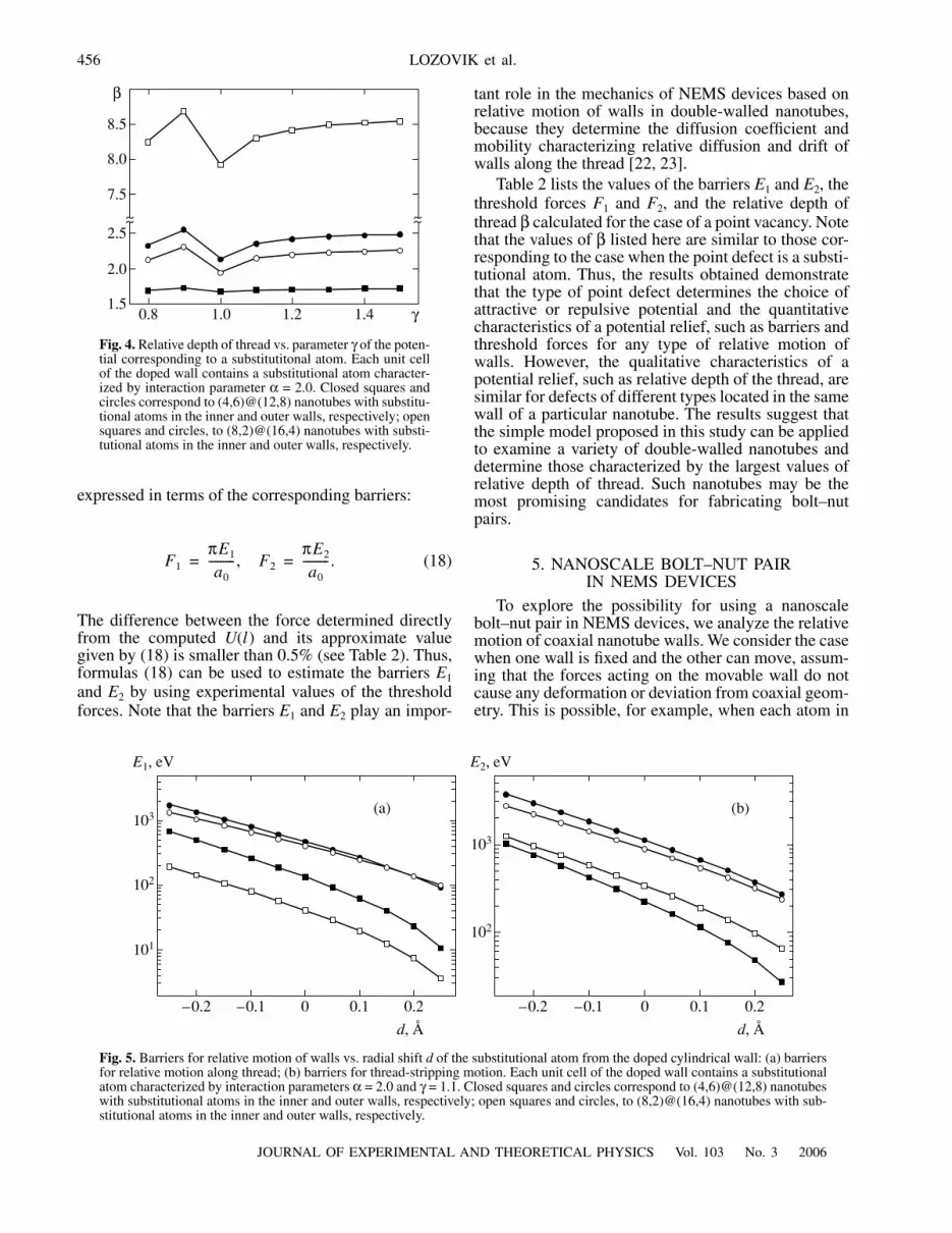
As mentioned above, the shape of potential energysurface is independent of α and weakly depends on γ(see Fig. 4).
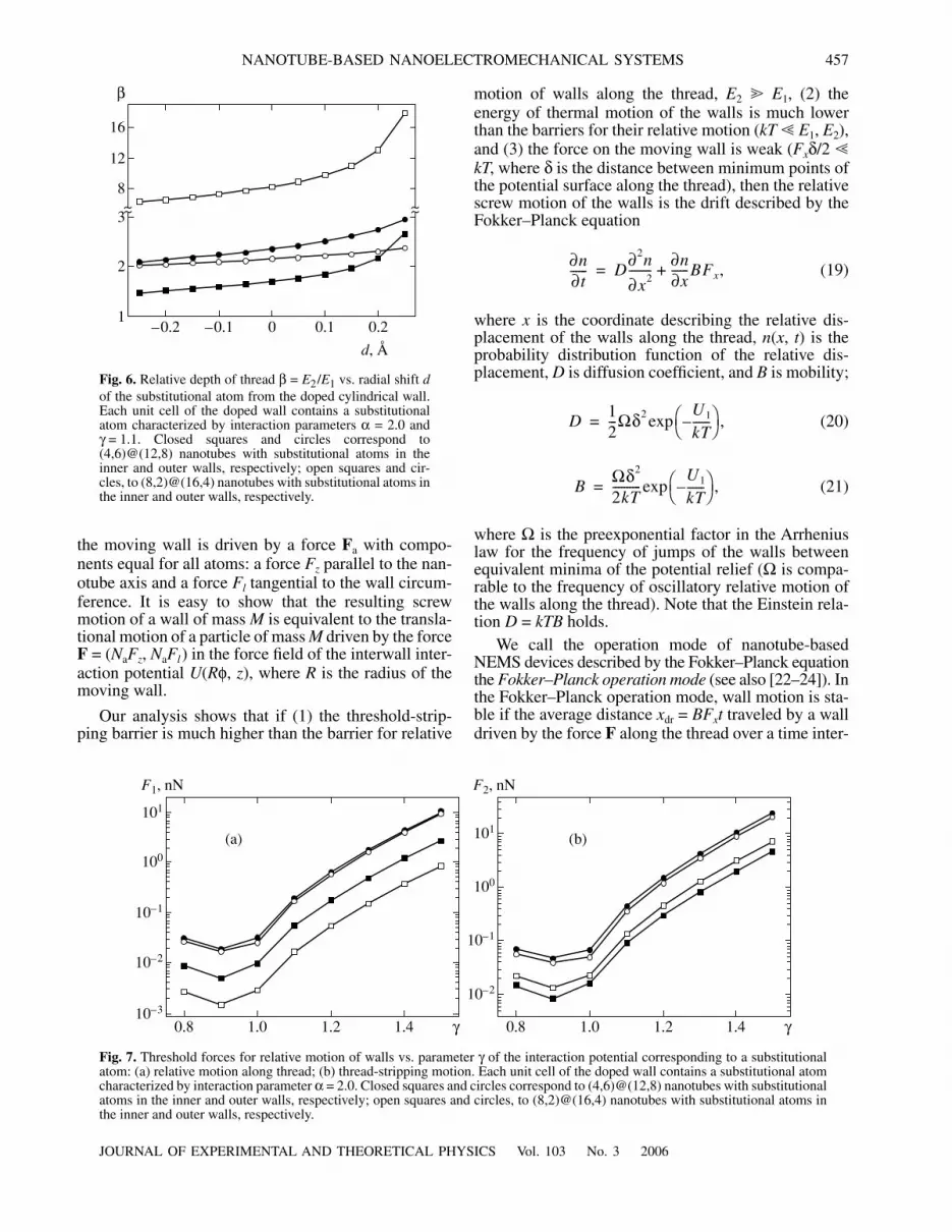
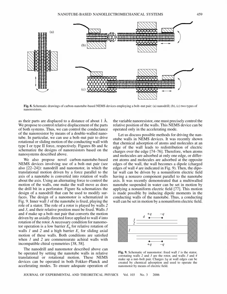
We also examined the case when the substitutionalatom is radially shifted from the location of the substi-tuted carbon atom. Figure 5 shows the barriers E1 andE2 as functions of the radial shift of the substitutionalatom. Its interaction with the other wall decreases withincreasing shift, and so do both E1 and E2. Figure 6shows the relative depth of thread β as a function of theshift of the substitutional atom. To date, boron- andnitrogen-doped nanotubes were obtained in [42–44]
and [42], respectively. Computations of the structure ofa doped single-walled nanotube show that the radialshift of the substitutional atom is less than 0.02 Å fornitrogen and 0.11 Å for boron [48]. Thus, Figure 6demonstrates that the corresponding changes in relativedepth of the thread are insignificant.
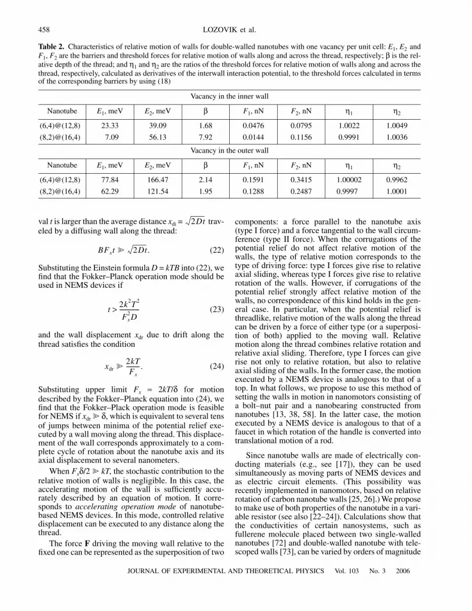
Since there exists a barrier for any relative motion ofnanotube walls, the motion is possible only if the driv-ing force exceeds a certain threshold. The thresholdforces F1 and F2 for relative motion along and acrossthe thread were defined in [22] as the highest deriva-tives of the interwall interaction energy U with respectto the coordinate l of displacement along the corre-sponding direction of rotational motion in the coordi-nate system (L, z). Figure 7 shows the threshold forcesF1 and F2 versus γ. Similarly to the barriers E1 and E2,these curves have distinct portions (γ < 1 and γ > 1),which are associated with attractive and repulsivepotential reliefs and can be approximated as const · γ12
at γ > 1.2. Note that the computed threshold forces liewithin the range of forces used in atomic force micros-copy [71].
Since the computed functions U(l) are very similarto cosines, the threshold forces can be approximately
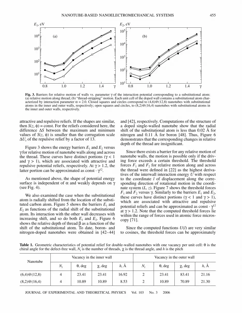
Table 1. Geometric characteristics of potential relief for double-walled nanotubes with one vacancy per unit cell: θ is thechiral angle for the defect-free wall, Nt is the number of threads, χ is the thread angle, and h is the pitch
NanotubeVacancy in the inner wall Vacancy in the outer wall
Nt θ, deg χ, deg h, Å Nt θ, deg χ, deg h, Å
(6,4)@(12,8) 4 23.41 23.41 16.92 2 23.41 83.41 21.16
(8,2)@(16,4) 4 10.89 10.89 8.53 2 10.89 70.89 21.30
0.8
102
0.8
102
1.0 1.2 1.4
103
104
101
E1, eV
(a) (b)
γ 1.0 1.2 1.4 γ101
103
104
105
E2, eV
Fig. 3. Barriers for relative motion of walls vs. parameter γ of the interaction potential corresponding to a substitutional atom:(a) relative motion along thread; (b) “thread-stripping” motion. Each unit cell of the doped wall contains a substitutional atom char-acterized by interaction parameter α = 2.0. Closed squares and circles correspond to (4,6)@(12,8) nanotubes with substitutionalatoms in the inner and outer walls, respectively; open squares and circles, to (8,2)@(16,4) nanotubes with substitutional atoms inthe inner and outer walls, respectively.
456
JOURNAL OF EXPERIMENTAL AND THEORETICAL PHYSICS Vol. 103 No. 3 2006
LOZOVIK et al.
expressed in terms of the corresponding barriers:
(18)
The difference between the force determined directlyfrom the computed U(l) and its approximate valuegiven by (18) is smaller than 0.5% (see Table 2). Thus,formulas (18) can be used to estimate the barriers E1and E2 by using experimental values of the thresholdforces. Note that the barriers E1 and E2 play an impor-
F1
πE1
a0---------, F2
πE2
a0---------.= =
tant role in the mechanics of NEMS devices based onrelative motion of walls in double-walled nanotubes,because they determine the diffusion coefficient andmobility characterizing relative diffusion and drift ofwalls along the thread [22, 23].
Table 2 lists the values of the barriers E1 and E2, thethreshold forces F1 and F2, and the relative depth ofthread β calculated for the case of a point vacancy. Notethat the values of β listed here are similar to those cor-responding to the case when the point defect is a substi-tutional atom. Thus, the results obtained demonstratethat the type of point defect determines the choice ofattractive or repulsive potential and the quantitativecharacteristics of a potential relief, such as barriers andthreshold forces for any type of relative motion ofwalls. However, the qualitative characteristics of apotential relief, such as relative depth of the thread, aresimilar for defects of different types located in the samewall of a particular nanotube. The results suggest thatthe simple model proposed in this study can be appliedto examine a variety of double-walled nanotubes anddetermine those characterized by the largest values ofrelative depth of thread. Such nanotubes may be themost promising candidates for fabricating bolt–nutpairs.
5. NANOSCALE BOLT–NUT PAIRIN NEMS DEVICES
To explore the possibility for using a nanoscalebolt–nut pair in NEMS devices, we analyze the relativemotion of coaxial nanotube walls. We consider the casewhen one wall is fixed and the other can move, assum-ing that the forces acting on the movable wall do notcause any deformation or deviation from coaxial geom-etry. This is possible, for example, when each atom in
0.8
2.0
1.0 1.2 1.4 γ1.5
2.5
7.5
8.0
8.5
~~ ~~
β
Fig. 4. Relative depth of thread vs. parameter γ of the poten-tial corresponding to a substitutitonal atom. Each unit cellof the doped wall contains a substitutional atom character-ized by interaction parameter α = 2.0. Closed squares andcircles correspond to (4,6)@(12,8) nanotubes with substitu-tional atoms in the inner and outer walls, respectively; opensquares and circles, to (8,2)@(16,4) nanotubes with substi-tutional atoms in the inner and outer walls, respectively.
–0.2
102
–0.1 0 0.1 0.2
d, Å
103
101
E1, eV
(a)
103
–0.1 0–0.2 0.1 0.2
(b)
102
E2, eV
d, Å
Fig. 5. Barriers for relative motion of walls vs. radial shift d of the substitutional atom from the doped cylindrical wall: (a) barriersfor relative motion along thread; (b) barriers for thread-stripping motion. Each unit cell of the doped wall contains a substitutionalatom characterized by interaction parameters α = 2.0 and γ = 1.1. Closed squares and circles correspond to (4,6)@(12,8) nanotubeswith substitutional atoms in the inner and outer walls, respectively; open squares and circles, to (8,2)@(16,4) nanotubes with sub-stitutional atoms in the inner and outer walls, respectively.
JOURNAL OF EXPERIMENTAL AND THEORETICAL PHYSICS Vol. 103 No. 3 2006
NANOTUBE-BASED NANOELECTROMECHANICAL SYSTEMS 457
the moving wall is driven by a force Fa with compo-nents equal for all atoms: a force Fz parallel to the nan-otube axis and a force Fl tangential to the wall circum-ference. It is easy to show that the resulting screwmotion of a wall of mass M is equivalent to the transla-tional motion of a particle of mass M driven by the forceF = (NaFz, NaFl) in the force field of the interwall inter-action potential U(Rφ, z), where R is the radius of themoving wall.
Our analysis shows that if (1) the threshold-strip-ping barrier is much higher than the barrier for relative
motion of walls along the thread, E2 E1, (2) theenergy of thermal motion of the walls is much lowerthan the barriers for their relative motion (kT E1, E2),and (3) the force on the moving wall is weak (Fxδ/2 kT, where δ is the distance between minimum points ofthe potential surface along the thread), then the relativescrew motion of the walls is the drift described by theFokker–Planck equation
(19)
where x is the coordinate describing the relative dis-placement of the walls along the thread, n(x, t) is theprobability distribution function of the relative dis-placement, D is diffusion coefficient, and B is mobility;
(20)
(21)
where Ω is the preexponential factor in the Arrheniuslaw for the frequency of jumps of the walls betweenequivalent minima of the potential relief (Ω is compa-rable to the frequency of oscillatory relative motion ofthe walls along the thread). Note that the Einstein rela-tion D = kTB holds.
We call the operation mode of nanotube-basedNEMS devices described by the Fokker–Planck equationthe Fokker–Planck operation mode (see also [22–24]). Inthe Fokker–Planck operation mode, wall motion is sta-ble if the average distance xdr = BFxt traveled by a walldriven by the force F along the thread over a time inter-
∂n∂t------ D
∂2n
∂x2-------- ∂n
∂x------BFx,+=
D12---Ωδ2 U1
kT------–⎝ ⎠
⎛ ⎞ ,exp=
BΩδ2
2kT----------
U1
kT------–⎝ ⎠
⎛ ⎞ ,exp=
–0.2
2
–0.1 0 0.1 0.2
d, Å
1
3
8
12
16
β
~~ ~~
Fig. 6. Relative depth of thread β = E2/E1 vs. radial shift dof the substitutional atom from the doped cylindrical wall.Each unit cell of the doped wall contains a substitutionalatom characterized by interaction parameters α = 2.0 andγ = 1.1. Closed squares and circles correspond to(4,6)@(12,8) nanotubes with substitutional atoms in theinner and outer walls, respectively; open squares and cir-cles, to (8,2)@(16,4) nanotubes with substitutional atoms inthe inner and outer walls, respectively.
0.8
10–1
0.8
10–1
1.0 1.2 1.4 γ
100
101
10–2
10–3
F1, nN
(a) (b)
1.0 1.2 1.4
100
101
10–2
F2, nN
γ
Fig. 7. Threshold forces for relative motion of walls vs. parameter γ of the interaction potential corresponding to a substitutionalatom: (a) relative motion along thread; (b) thread-stripping motion. Each unit cell of the doped wall contains a substitutional atomcharacterized by interaction parameter α = 2.0. Closed squares and circles correspond to (4,6)@(12,8) nanotubes with substitutionalatoms in the inner and outer walls, respectively; open squares and circles, to (8,2)@(16,4) nanotubes with substitutional atoms inthe inner and outer walls, respectively.
458
JOURNAL OF EXPERIMENTAL AND THEORETICAL PHYSICS Vol. 103 No. 3 2006
LOZOVIK et al.
val t is larger than the average distance xdi = trav-eled by a diffusing wall along the thread:
(22)
Substituting the Einstein formula D = kTB into (22), wefind that the Fokker–Planck operation mode should beused in NEMS devices if
(23)
and the wall displacement xdr due to drift along thethread satisfies the condition
(24)
Substituting upper limit Fx ≈ 2kT/δ for motiondescribed by the Fokker–Planck equation into (24), wefind that the Fokker–Plack operation mode is feasiblefor NEMS if xdr δ, which is equivalent to several tensof jumps between minima of the potential relief exe-cuted by a wall moving along the thread. This displace-ment of the wall corresponds approximately to a com-plete cycle of rotation about the nanotube axis and itsaxial displacement to several nanometers.
When Fxδ/2 kT, the stochastic contribution to therelative motion of walls is negligible. In this case, theaccelerating motion of the wall is sufficiently accu-rately described by an equation of motion. It corre-sponds to accelerating operation mode of nanotube-based NEMS devices. In this mode, controlled relativedisplacement can be executed to any distance along thethread.
The force F driving the moving wall relative to thefixed one can be represented as the superposition of two
2Dt
BFxt 2Dt.
t2k2T2
Fx2D
-------------->
xdr 2kTFx
---------.
components: a force parallel to the nanotube axis(type I force) and a force tangential to the wall circum-ference (type II force). When the corrugations of thepotential relief do not affect relative motion of thewalls, the type of relative motion corresponds to thetype of driving force: type I forces give rise to relativeaxial sliding, whereas type I forces give rise to relativerotation of the walls. However, if corrugations of thepotential relief strongly affect relative motion of thewalls, no correspondence of this kind holds in the gen-eral case. In particular, when the potential relief isthreadlike, relative motion of the walls along the threadcan be driven by a force of either type (or a superposi-tion of both) applied to the moving wall. Relativemotion along the thread combines relative rotation andrelative axial sliding. Therefore, type I forces can giverise not only to relative rotation, but also to relativeaxial sliding of the walls. In the former case, the motionexecuted by a NEMS device is analogous to that of atop. In what follows, we propose to use this method ofsetting the walls in motion in nanomotors consisting ofa bolt–nut pair and a nanobearing constructed fromnanotubes [13, 38, 58]. In the latter case, the motionexecuted by a NEMS device is analogous to that of afaucet in which rotation of the handle is converted intotranslational motion of a rod.
Since nanotube walls are made of electrically con-ducting materials (e.g., see [17]), they can be usedsimultaneously as moving parts of NEMS devices andas electric circuit elements. (This possibility wasrecently implemented in nanomotors, based on relativerotation of carbon nanotube walls [25, 26].) We proposeto make use of both properties of the nanotube in a vari-able resistor (see also [22–24]). Calculations show thatthe conductivities of certain nanosystems, such asfullerene molecule placed between two single-wallednanotubes [72] and double-walled nanotube with tele-scoped walls [73], can be varied by orders of magnitude
Table 2. Characteristics of relative motion of walls for double-walled nanotubes with one vacancy per unit cell: E1, E2 andF1, F2 are the barriers and threshold forces for relative motion of walls along and across the thread, respectively; β is the rel-ative depth of the thread; and η1 and η2 are the ratios of the threshold forces for relative motion of walls along and across thethread, respectively, calculated as derivatives of the interwall interaction potential, to the threshold forces calculated in termsof the corresponding barriers by using (18)
Vacancy in the inner wall
Nanotube E1, meV E2, meV β F1, nN F2, nN η1 η2
(6,4)@(12,8) 23.33 39.09 1.68 0.0476 0.0795 1.0022 1.0049
(8,2)@(16,4) 7.09 56.13 7.92 0.0144 0.1156 0.9991 1.0036
Vacancy in the outer wall
Nanotube E1, meV E2, meV β F1, nN F2, nN η1 η2
(6,4)@(12,8) 77.84 166.47 2.14 0.1591 0.3415 1.00002 0.9962
(8,2)@(16,4) 62.29 121.54 1.95 0.1288 0.2487 0.9997 1.0001
JOURNAL OF EXPERIMENTAL AND THEORETICAL PHYSICS Vol. 103 No. 3 2006
NANOTUBE-BASED NANOELECTROMECHANICAL SYSTEMS 459
as their parts are displaced to a distance of about 1 Å.We propose to control relative displacement of the partsof both systems. Thus, we can control the conductanceof the nanoresistor by means of a double-walled nano-tube. In particular, we can use a bolt–nut pair to driverotational or sliding motion of the conducting wall withtype I or type II force, respectively. Figures 8b and 8cschematize the designs of nanoresistors based on thenanosystems described above.
We also propose novel carbon-nanotube-basedNEMS devices involving use of a bolt–nut pair (seealso [22–24]): nanodrill and nanomotor, in which thetranslational motion driven by a force parallel to theaxis of a nanotube is converted into rotation of wallsabout the axis. Using an alternating force to control themotion of the walls, one make the wall move as doesthe drill bit in a perforator. Figure 8a schematizes thedesign of a nanodrill that can be used to modify sur-faces. The design of a nanomotor is schematized inFig. 9. Inner wall 1 of the nanotube is fixed, playing therole of a stator. The role of a rotor is played by walls 2and 3, and their relative position must be fixed. Walls 3and 4 make up a bolt–nut pair that converts the motiondriven by an axially directed force applied to wall 4 intorotation of the rotor. A necessary condition for nanomo-tor operation is a low barrier Eφ for relative rotation ofwalls 1 and 2 and a high barrier Ez for sliding axialmotion of these walls. Both conditions are satisfiedwhen 1 and 2 are commensurate achiral walls withincompatible chiral symmetries [38, 58].
The nanodrill and nanomotor described above canbe operated by setting the nanotube walls in relativetranslational or rotational motion. These NEMSdevices can be operated in both Fokker–Planck andaccelerating modes. To ensure adequate operation of
the variable nanoresistor, one must precisely control therelative position of the walls. This NEMS device can beoperated only in the accelerating mode.
Let us discuss possible methods for driving the nan-otube walls in NEMS devices. It was recently shownthat chemical adsorption of atoms and molecules at anedge of the wall leads to redistribution of electriccharges over the edge [74–76]. Therefore, when atomsand molecules are adsorbed at only one edge, or differ-ent atoms and molecules are adsorbed at the oppositeedges of the wall, the wall becomes a dipole (chargededges of wall 4 are indicated in Fig. 9). Then, the dipo-lar wall can be driven by a nonuniform electric fieldhaving a nonzero component parallel to the nanotubeaxis. It was recently demonstrated that a multiwallednanotube suspended in water can be set in motion byapplying a nonuniform electric field [77]. This motionis made possible by inducing dipole moments in theconducting walls of the nanotube. Thus, a conductingwall can be set in motion by a nonuniform electric field.
(a)
(b)
(c)
Fig. 8. Schematic drawings of carbon-nanotube-based NEMS devices employing a bolt–nut pair: (a) nanodrill; (b), (c) two types ofnanoresistors.
1
23
+q
+q
–q
–q
Fig. 9. Schematic of nanomotor: fixed wall 1 is the stator,corotating walls 2 and 3 are the rotor, and walls 3 and 4make up a nut–bolt pair. Charges ±q at wall edges can becreated by chemical adsorption and used to operate thenanomotor by means of electric field.
4
460
JOURNAL OF EXPERIMENTAL AND THEORETICAL PHYSICS Vol. 103 No. 3 2006
LOZOVIK et al.
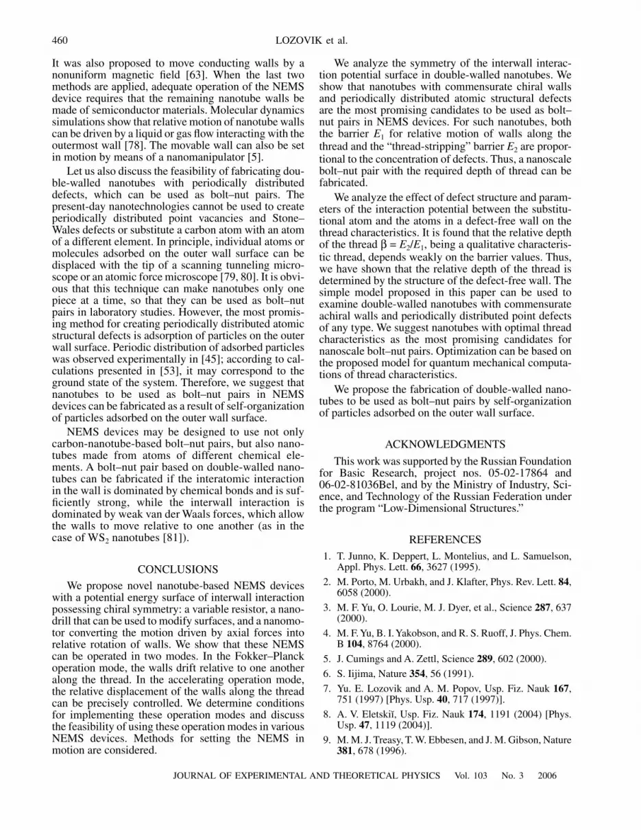
It was also proposed to move conducting walls by anonuniform magnetic field [63]. When the last twomethods are applied, adequate operation of the NEMSdevice requires that the remaining nanotube walls bemade of semiconductor materials. Molecular dynamicssimulations show that relative motion of nanotube wallscan be driven by a liquid or gas flow interacting with theoutermost wall [78]. The movable wall can also be setin motion by means of a nanomanipulator [5].
Let us also discuss the feasibility of fabricating dou-ble-walled nanotubes with periodically distributeddefects, which can be used as bolt–nut pairs. Thepresent-day nanotechnologies cannot be used to createperiodically distributed point vacancies and Stone–Wales defects or substitute a carbon atom with an atomof a different element. In principle, individual atoms ormolecules adsorbed on the outer wall surface can bedisplaced with the tip of a scanning tunneling micro-scope or an atomic force microscope [79, 80]. It is obvi-ous that this technique can make nanotubes only onepiece at a time, so that they can be used as bolt–nutpairs in laboratory studies. However, the most promis-ing method for creating periodically distributed atomicstructural defects is adsorption of particles on the outerwall surface. Periodic distribution of adsorbed particleswas observed experimentally in [45]; according to cal-culations presented in [53], it may correspond to theground state of the system. Therefore, we suggest thatnanotubes to be used as bolt–nut pairs in NEMSdevices can be fabricated as a result of self-organizationof particles adsorbed on the outer wall surface.
NEMS devices may be designed to use not onlycarbon-nanotube-based bolt–nut pairs, but also nano-tubes made from atoms of different chemical ele-ments. A bolt–nut pair based on double-walled nano-tubes can be fabricated if the interatomic interactionin the wall is dominated by chemical bonds and is suf-ficiently strong, while the interwall interaction isdominated by weak van der Waals forces, which allowthe walls to move relative to one another (as in thecase of WS2 nanotubes [81]).
CONCLUSIONS
We propose novel nanotube-based NEMS deviceswith a potential energy surface of interwall interactionpossessing chiral symmetry: a variable resistor, a nano-drill that can be used to modify surfaces, and a nanomo-tor converting the motion driven by axial forces intorelative rotation of walls. We show that these NEMScan be operated in two modes. In the Fokker–Planckoperation mode, the walls drift relative to one anotheralong the thread. In the accelerating operation mode,the relative displacement of the walls along the threadcan be precisely controlled. We determine conditionsfor implementing these operation modes and discussthe feasibility of using these operation modes in variousNEMS devices. Methods for setting the NEMS inmotion are considered.
We analyze the symmetry of the interwall interac-tion potential surface in double-walled nanotubes. Weshow that nanotubes with commensurate chiral wallsand periodically distributed atomic structural defectsare the most promising candidates to be used as bolt–nut pairs in NEMS devices. For such nanotubes, boththe barrier E1 for relative motion of walls along thethread and the “thread-stripping” barrier E2 are propor-tional to the concentration of defects. Thus, a nanoscalebolt–nut pair with the required depth of thread can befabricated.
We analyze the effect of defect structure and param-eters of the interaction potential between the substitu-tional atom and the atoms in a defect-free wall on thethread characteristics. It is found that the relative depthof the thread β = E2/E1, being a qualitative characteris-tic thread, depends weakly on the barrier values. Thus,we have shown that the relative depth of the thread isdetermined by the structure of the defect-free wall. Thesimple model proposed in this paper can be used toexamine double-walled nanotubes with commensurateachiral walls and periodically distributed point defectsof any type. We suggest nanotubes with optimal threadcharacteristics as the most promising candidates fornanoscale bolt–nut pairs. Optimization can be based onthe proposed model for quantum mechanical computa-tions of thread characteristics.
We propose the fabrication of double-walled nano-tubes to be used as bolt–nut pairs by self-organizationof particles adsorbed on the outer wall surface.
ACKNOWLEDGMENTS
This work was supported by the Russian Foundationfor Basic Research, project nos. 05-02-17864 and06-02-81036Bel, and by the Ministry of Industry, Sci-ence, and Technology of the Russian Federation underthe program “Low-Dimensional Structures.”
REFERENCES
1. T. Junno, K. Deppert, L. Montelius, and L. Samuelson,Appl. Phys. Lett. 66, 3627 (1995).
2. M. Porto, M. Urbakh, and J. Klafter, Phys. Rev. Lett. 84,6058 (2000).
3. M. F. Yu, O. Lourie, M. J. Dyer, et al., Science 287, 637(2000).
4. M. F. Yu, B. I. Yakobson, and R. S. Ruoff, J. Phys. Chem.B 104, 8764 (2000).
5. J. Cumings and A. Zettl, Science 289, 602 (2000).
6. S. Iijima, Nature 354, 56 (1991).
7. Yu. E. Lozovik and A. M. Popov, Usp. Fiz. Nauk 167,751 (1997) [Phys. Usp. 40, 717 (1997)].
8. A. V. Eletskiœ, Usp. Fiz. Nauk 174, 1191 (2004) [Phys.Usp. 47, 1119 (2004)].
9. M. M. J. Treasy, T. W. Ebbesen, and J. M. Gibson, Nature381, 678 (1996).

JOURNAL OF EXPERIMENTAL AND THEORETICAL PHYSICS Vol. 103 No. 3 2006
NANOTUBE-BASED NANOELECTROMECHANICAL SYSTEMS 461
10. E. W. Wong, P. E. Sheehan, and C. M. Lieber, Science277, 1971 (1997).
11. A. Krishnan, E. Dujardin, T. W. Ebbesen, et al., Phys.Rev. B 58, 14013 (1998).
12. P. Poncharat, Z. L. Wang, D. Ugarte, and W. A. de Heer,Science 283, 1513 (1999).
13. R. E. Tuzun, D. W. Noid, and B. G. Sumpter, Nanotech-nology 6, 52 (1995).
14. D. Srivastava, Nanotechnology 8, 186 (1997).15. L. Forro, Science 289, 5479 (2000).16. Q. Zheng and Q. Jiang, Phys. Rev. Lett. 88, 045503
(2002).17. R. Saito, M. Fujita, G. Dresselhaus, and M. S. Dressel-
haus, Appl. Phys. Lett. 60, 2204 (1992).18. S. J. Tans, A. R. M. Verschueren, and C. Dekker, Nature
393, 49 (1998).19. R. Tamura, Phys. Rev. B 64, 201404(R) (2001).20. T. Rueches, P. Kim, E. Joselevich, et al., Science 289, 94
(2000).21. M. Menon, A. N. Andriotis, D. Srivastava, et al., Phys.
Rev. Lett. 91, 145501 (2003).22. Yu. E. Lozovik, A. V. Minogin, and A. M. Popov, Phys.
Lett. A 313, 112 (2003).23. Yu. E. Lozovik, A. V. Minogin, and A. M. Popov, Pis’ma
Zh. Éksp. Teor. Fiz. 77, 759 (2003) [JETP Lett. 77, 631(2003)].
24. Yu. E. Lozovik and A. M. Popov, Fullerenes NanotubesCarbon Nanostruct. 12, 485 (2004).
25. A. M. Fennimore, T. D. Yuzvinsky, W. Q. Han, et al.,Nature 424, 408 (2003).
26. B. Bourlon, D. C. Glatti, L. Forro, and A. Bachfold,Nano Lett. 4, 709 (2004).
27. R. Saito, R. Matsuo, T. Kimura, et al., Chem. Phys. Lett.348, 187 (2001).
28. T. W. Ebbesen and P. M. Ajayan, Nature 358, 220 (1992).29. J. L. Hutchison, N. A. Kiselev, E. P. Krinichnaya, et al.,
Carbon 39, 761 (2001).30. L. Ci, Z. Pao, Z. Zhou, et al., Chem. Phys. Lett. 359, 63
(2002).31. W. Ren, F. Li, J. Chen, et al., Chem. Phys. Lett. 359, 196
(2002).32. S. Bandow, M. Takizawa, K. Hirahara, et al., Chem.
Phys. Lett. 337, 48 (2001).33. J. Sloan, R. E. Dunin-Borkowski, J. L. Hutchison, et al.,
Chem. Phys. Lett. 316, 191 (2000).34. C. T. White, D. H. Robertson, and J. W. Mintmire, Phys.
Rev. B 47, 5485 (1993).35. R. A. Jishi, M. S. Dresselhaus, and G. Dresselhaus, Phys.
Rev. B 47, 16671 (1993).36. A. N. Kolmogorov and V. H. Crespi, Phys. Rev. Lett. 85,
4727 (2000).
37. T. Vukovi , M. Damnjanovi , and I. Milo evi , PhysicaE (Amsterdam) 16, 269 (2003).
38. A. V. Belikov, A. G. Nikolaev, Yu. E. Lozovik, andA. M. Popov, Chem. Phys. Lett. 385, 72 (2004).
c
^
c
^
s° c
^
39. M. Damnjanovi , T. Vukovi , and I. Milo evi , Eur.Phys. J. B 25, 131 (2002).
40. E. Bichoutskaia, A. M. Popov, A. El-Barbary, et al.,Phys. Rev. B 71, 113403 (2005).
41. A. V. Belikov, A. G. Nikolaev, Yu. E. Lozovik, andA. M. Popov, Fullerenes Nanotubes Carbon Nanostruct.12, 117 (2004).
42. O. Stephan, P. M. Ajayan, C. Colliex, et al., Science 266,1683 (1994).
43. D. L. Carroll, Ph. Redlich, X. Blase, et al., Phys. Rev.Lett. 81, 2332 (1998).
44. K. Liu, Ph. Avonris, R. Martel, and W. K. Hsu, Phys.Rev. B 63, 161404(R) (2001).
45. H. Ago, R. Azumi, S. Ohshima, et al., Chem. Phys. Lett.383, 469 (2004).
46. H. J. Choi, J. Ihm, S. G. Lonie, and M. L. Cohen, Phys.Rev. Lett. 84, 2917 (2000).
47. H. F. Bettinger, T. Dumitrica, G. E. Scuceria, andB. I. Yakobson, Phys. Rev. B 65, 041406 (2002).
48. J.-Y. Li and J. Bernholc, Phys. Rev. B 47, 1708 (1993).49. P. E. Lammert, V. H. Crespi, and A. Rubio, Phys. Rev.
Lett. 87, 136402 (2001).50. A. H. Hevidomskyy, G. Csanyi, and M. C. Payne, Phys.
Rev. Lett. 91, 105502 (2003).51. R. J. Baieriee, S. B. Fagan, R. Mota, et al., Phys. Rev. B
64, 085413 (2001).52. S. P. Walch, Chem. Phys. Lett. 374, 501 (2003).53. K. A. Park, Y. S. Choi, and Y. H. Lee, Phys. Rev. B 68,
045429 (2003).
54. M. Damnjanovi , I. Milo evi , T. Vukovi , and R. Sre-danovi , Phys. Rev. B 60, 2728 (1999).
55. Yu. E. Lozovik, A. M. Popov, and A. V. Belikov, Fiz.Tverd. Tela (St. Petersburg) 45, 1333 (2003) [Phys. SolidState 45, 1396 (2003)].
56. L. X. Benedict, N. G. Chopra, M. L. Cohen, et al., Chem.Phys. Lett. 286, 490 (1998).
57. J.-C. Charlier and J. P. Michenaud, Phys. Rev. Lett. 70,1858 (1993).
58. E. Bichoutskaia, A. M. Popov, M. I. Heggie, andYu. E. Lozovik, Phys. Rev. B 73, 045435 (2006).
59. A. H. R. Palser, Phys. Chem. Chem. Phys. 1, 4459(1999).
60. J. P. Lu, X. P. Li, and R. M. Martin, Phys. Rev. Lett. 68,1551 (1992).
61. M. Damnjanovi , E. Dobard i , I. Milo evi , et al., NewJ. Phys. 5, 148.1 (2003).
62. S. B. Legoas, V. R. Coluci, S. F. Braga, et al., Phys. Rev.Lett. 90, 055504 (2003).
63. S. B. Legoas, V. R. Coluci, S. F. Braga, et al., Nanotech-nology 15, 184 (2004).
64. W. Guo, Y. Guo, H. Gao, et al., Phys. Rev. Lett. 91,125501 (2003).
65. Y. Zhao, C.-C. Ma, G. Chen, and Q. Jiang, Phys. Rev.Lett. 91, 175504 (2003).
66. J. L. Rivera, C. McCabe, and P. P. Cummings, Nano Lett.3, 1001 (2003).
c
^
c
^
s° c
^
c
^
s° c
^
c
^
c
^
c
^
z° c
^
s° c
^

462
JOURNAL OF EXPERIMENTAL AND THEORETICAL PHYSICS Vol. 103 No. 3 2006
LOZOVIK et al.
67. J. W. Kang and H. J. Hwang, J. Appl. Phys. 96, 3900(2004).
68. Yu. E. Lozovik and A. M. Popov, Chem. Phys. Lett. 328,355 (2000).
69. Yu. E. Lozovik and A. M. Popov, Fiz. Tverd. Tela (St.Petersburg) 44, 180 (2002) [Phys. Solid State 44, 186(2002)].
70. A. Burian, J. C. Dore, H. E. Fisher, and J. Sloan, Phys.Rev. B 59, 1665 (1999).
71. F. J. Giessibl, Rev. Mod. Phys. 75, 949 (2003).72. R. Guttierrez, G. Fagas, G. Cuniberti, et al., Phys. Rev. B
65, 113410 (2002).73. D. H. Kim and K. J. Chang, Phys. Rev. B 66, 155402
(2002).74. J. S. Murray, P. Lane, M. C. Concha, and P. Politzer, in
Nano and Giga Challenges in Microelectronics: Book ofAbstracts (Cracow, Poland, 2004), p. 175.
75. Y. G. Hwang and Y. H. Lee, J. Korean Phys. Soc. 42, 267(2005).
76. N. Park, Y. Miyamoto, K. Lee, et al., Chem. Phys. Lett.403, 135 (2005).
77. D. L. Fan, F. Q. Zhu, R. C. Cammarata, and C. L. Chien,Phys. Rev. Lett. 94, 247208 (2005).
78. J. W. Kang and H. J. Hwang, Nanotechnology 15, 1633(2004).
79. D. M. Eigler and E. K. Schweizer, Nature 344, 525(1990).
80. M. F. Crommie, C. Plutz, and D. M. Eigler, Science 262,218 (1993).
81. R. Tenne, L. Margulis, M. Genut, and G. Hodes, Nature360, 445 (1992).
Translated by A. Betev