nanometrology using a through-focus scanning optical microscopy method
TRANSCRIPT

This content has been downloaded from IOPscience. Please scroll down to see the full text.
Download details:
IP Address: 155.97.178.73
This content was downloaded on 01/07/2014 at 08:24
Please note that terms and conditions apply.
Nanometrology using a through-focus scanning optical microscopy method
View the table of contents for this issue, or go to the journal homepage for more
2011 Meas. Sci. Technol. 22 024002
(http://iopscience.iop.org/0957-0233/22/2/024002)
Home Search Collections Journals About Contact us My IOPscience

IOP PUBLISHING MEASUREMENT SCIENCE AND TECHNOLOGY
Meas. Sci. Technol. 22 (2011) 024002 (10pp) doi:10.1088/0957-0233/22/2/024002
Nanometrology using a through-focusscanning optical microscopy methodRavikiran Attota and Richard Silver
National Institute of Standards and Technology, Gaithersburg, MD 20899, USA
E-mail: [email protected]
Received 1 April 2010, in final form 9 June 2010Published 21 December 2010Online at stacks.iop.org/MST/22/024002
AbstractWe present an initial review of a novel through-focus scanning optical microscopy (TSOMpronounced as ‘tee-som’) imaging method that produces nanometer-dimensional measurementsensitivity using a conventional bright-field optical microscope. In the TSOM method a targetis scanned through the focus of an optical microscope, acquiring conventional optical imagesat different focal positions. The TSOM images are constructed using the through-focus opticalimages. A TSOM image is unique under given experimental conditions and is sensitive tochanges in the dimensions of a target in a distinct way. We use this characteristic fornanoscale-dimensional metrology. This technique can be used to identify the dimension whichis changing between two nanosized targets and to determine the dimensions using alibrary-matching method. This methodology has potential utility for a wide range of targetgeometries and application areas, including nanometrology, nanomanufacturing, defectanalysis, inspection, process control and biotechnology.
Keywords: TSOM, through-focus, optical microscope, nanometrology, process control,nanomanufacturing, nanoparticles, overlay metrology, critical dimension, defect analysis,dimensional analysis, MEMS, NEMS
1. Introduction
The demand on tools to make measurements at the nanoscaleis very high as dimensional information at the nanoscaleis required to enable progress in nanotechnology andnanosciences [1, 2]. Several tools, such as the atomic forcemicroscope (AFM), scanning tunneling microscope (STM)and scanning electron microscope (SEM), are routinely usedto provide measurements at this scale. However, withthe commercialization of nanotechnology, fast and reliablenanoscale feature measurements will become increasinglyimportant [1, 2]. Optics-based tools can be advantageousbecause they have a relatively low cost of ownership with highthroughput.
It is often a misconception that optical microscopes arenot well suited for dimensional measurements of features thatare smaller than half the wavelength of illumination (200 nmsized features in the visible region) due to diffraction [3]. Itis true that diffraction-dominated images make meaningfulanalysis of the targets difficult. However, this limitation canbe circumvented by (i) considering the image as a ‘signal’ that
represents the target, (ii) using a set of through-focus imagesinstead of one ‘best focus’ image and (iii) making use of highlydeveloped optical models [4–6].
In conventional optical microscopy, it is usually deemednecessary to acquire images at the ‘best focus’ position fora meaningful analysis, based on the belief that the mostfaithful representation of the target is rendered only at thebest focus position. However, the out-of-focus images docontain additional useful information regarding the target.This information may be obtained using an appropriate dataacquisition and analysis method. Based on this, and on theobservation of a distinct signature for different parametricvariations, we introduced a new method for nanoscale-dimensional analysis with nanometer sensitivity for three-dimensional, nanosized targets using a conventional bright-field optical microscope [7–12]. The method is referred toas the ‘through-focus scanning optical microscopy’ (TSOMpronounced as ‘tee-som’) imaging method. The TSOMmethod has won R&D 100 award for the year 2010 [13, 14].Here, we present an initial review of the TSOM method. TheTSOM method is applicable to three-dimensional targets, thus
0957-0233/11/024002+10$33.00 1 © 2011 IOP Publishing Ltd Printed in the UK & the USA
Meas. Sci. Technol. 22 (2011) 024002 R Attota and R Silver
(a) (b)
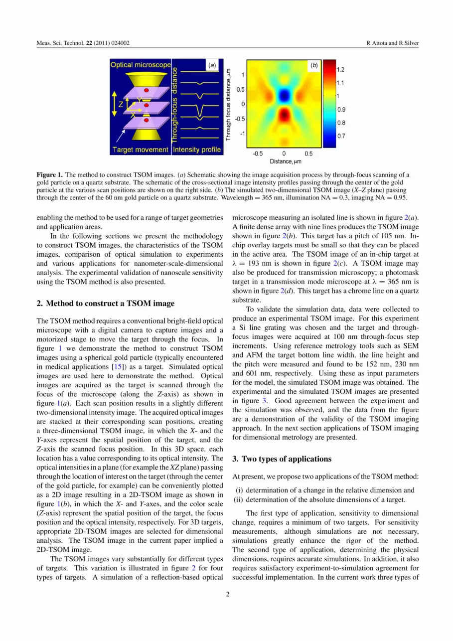
Figure 1. The method to construct TSOM images. (a) Schematic showing the image acquisition process by through-focus scanning of agold particle on a quartz substrate. The schematic of the cross-sectional image intensity profiles passing through the center of the goldparticle at the various scan positions are shown on the right side. (b) The simulated two-dimensional TSOM image (X–Z plane) passingthrough the center of the 60 nm gold particle on a quartz substrate. Wavelength = 365 nm, illumination NA = 0.3, imaging NA = 0.95.
enabling the method to be used for a range of target geometriesand application areas.
In the following sections we present the methodologyto construct TSOM images, the characteristics of the TSOMimages, comparison of optical simulation to experimentsand various applications for nanometer-scale-dimensionalanalysis. The experimental validation of nanoscale sensitivityusing the TSOM method is also presented.
2. Method to construct a TSOM image
The TSOM method requires a conventional bright-field opticalmicroscope with a digital camera to capture images and amotorized stage to move the target through the focus. Infigure 1 we demonstrate the method to construct TSOMimages using a spherical gold particle (typically encounteredin medical applications [15]) as a target. Simulated opticalimages are used here to demonstrate the method. Opticalimages are acquired as the target is scanned through thefocus of the microscope (along the Z-axis) as shown infigure 1(a). Each scan position results in a slightly differenttwo-dimensional intensity image. The acquired optical imagesare stacked at their corresponding scan positions, creatinga three-dimensional TSOM image, in which the X- and theY-axes represent the spatial position of the target, and theZ-axis the scanned focus position. In this 3D space, eachlocation has a value corresponding to its optical intensity. Theoptical intensities in a plane (for example the XZ plane) passingthrough the location of interest on the target (through the centerof the gold particle, for example) can be conveniently plottedas a 2D image resulting in a 2D-TSOM image as shown infigure 1(b), in which the X- and Y-axes, and the color scale(Z-axis) represent the spatial position of the target, the focusposition and the optical intensity, respectively. For 3D targets,appropriate 2D-TSOM images are selected for dimensionalanalysis. The TSOM image in the current paper implied a2D-TSOM image.
The TSOM images vary substantially for different typesof targets. This variation is illustrated in figure 2 for fourtypes of targets. A simulation of a reflection-based optical
microscope measuring an isolated line is shown in figure 2(a).A finite dense array with nine lines produces the TSOM imageshown in figure 2(b). This target has a pitch of 105 nm. In-chip overlay targets must be small so that they can be placedin the active area. The TSOM image of an in-chip target atλ = 193 nm is shown in figure 2(c). A TSOM image mayalso be produced for transmission microscopy; a photomasktarget in a transmission mode microscope at λ = 365 nm isshown in figure 2(d). This target has a chrome line on a quartzsubstrate.
To validate the simulation data, data were collected toproduce an experimental TSOM image. For this experimenta Si line grating was chosen and the target and through-focus images were acquired at 100 nm through-focus stepincrements. Using reference metrology tools such as SEMand AFM the target bottom line width, the line height andthe pitch were measured and found to be 152 nm, 230 nmand 601 nm, respectively. Using these as input parametersfor the model, the simulated TSOM image was obtained. Theexperimental and the simulated TSOM images are presentedin figure 3. Good agreement between the experiment andthe simulation was observed, and the data from the figureare a demonstration of the validity of the TSOM imagingapproach. In the next section applications of TSOM imagingfor dimensional metrology are presented.
3. Two types of applications
At present, we propose two applications of the TSOM method:
(i) determination of a change in the relative dimension and(ii) determination of the absolute dimensions of a target.
The first type of application, sensitivity to dimensionalchange, requires a minimum of two targets. For sensitivitymeasurements, although simulations are not necessary,simulations greatly enhance the rigor of the method.The second type of application, determining the physicaldimensions, requires accurate simulations. In addition, it alsorequires satisfactory experiment-to-simulation agreement forsuccessful implementation. In the current work three types of
2

Meas. Sci. Technol. 22 (2011) 024002 R Attota and R Silver
Figure 2. The simulated TSOM images for (a) an isolated Si line on a Si substrate (line width = 40 nm, line height = 100 nm, illuminationNA = 0.4, collection NA = 0.8 and illumination wavelength = 546 nm), (b) a finite dense Si array on a Si substrate (number of lines = 9,line width = 35 nm, pitch = 105 nm, line height = 100 nm, illumination NA = 0.3, collection NA = 0.8 and illumination wavelength =193 nm), (c) an in-chip Si line on a Si substrate overlay target (line width = 60 nm, line height = 100 nm, trench width = 60 nm, trenchdepth = 100 nm, distance between the lines = 400 nm, illumination NA = 0.2, collection NA = 0.8 and illumination wavelength = 193 nm)and (d) a chrome line on a quartz substrate photo mask in a transmission mode microscope (line width = 120 nm, line height = 100 nm,illumination NA = 0.1, collection NA = 0.8, illumination wavelength = 365 nm).
(a) (b)
Figure 3. Comparison of (a) the simulation and (b) the experimental TSOM images for a line grating. Line width = 152 nm, line height =230 nm, pitch = 601 nm, illumination NA = 0.36, collection NA = 0.8, illumination wavelength = 546 nm, a Si line on a Si substrate. Onlyone pitch distance is shown in the figure.
optical simulation programs were used [4–6]. The followingis a detailed discussion of these two applications of the TSOMimages.
3.1. Determination of a change in the relative dimension
A small change in the dimension of a target produces acorresponding change in the TSOM image. Comparing twoTSOM images from different targets, one can identify that achange in the target dimension has occurred. Although one
can compare and identify changes in different ways, here wepresent a method based on a differential TSOM image.
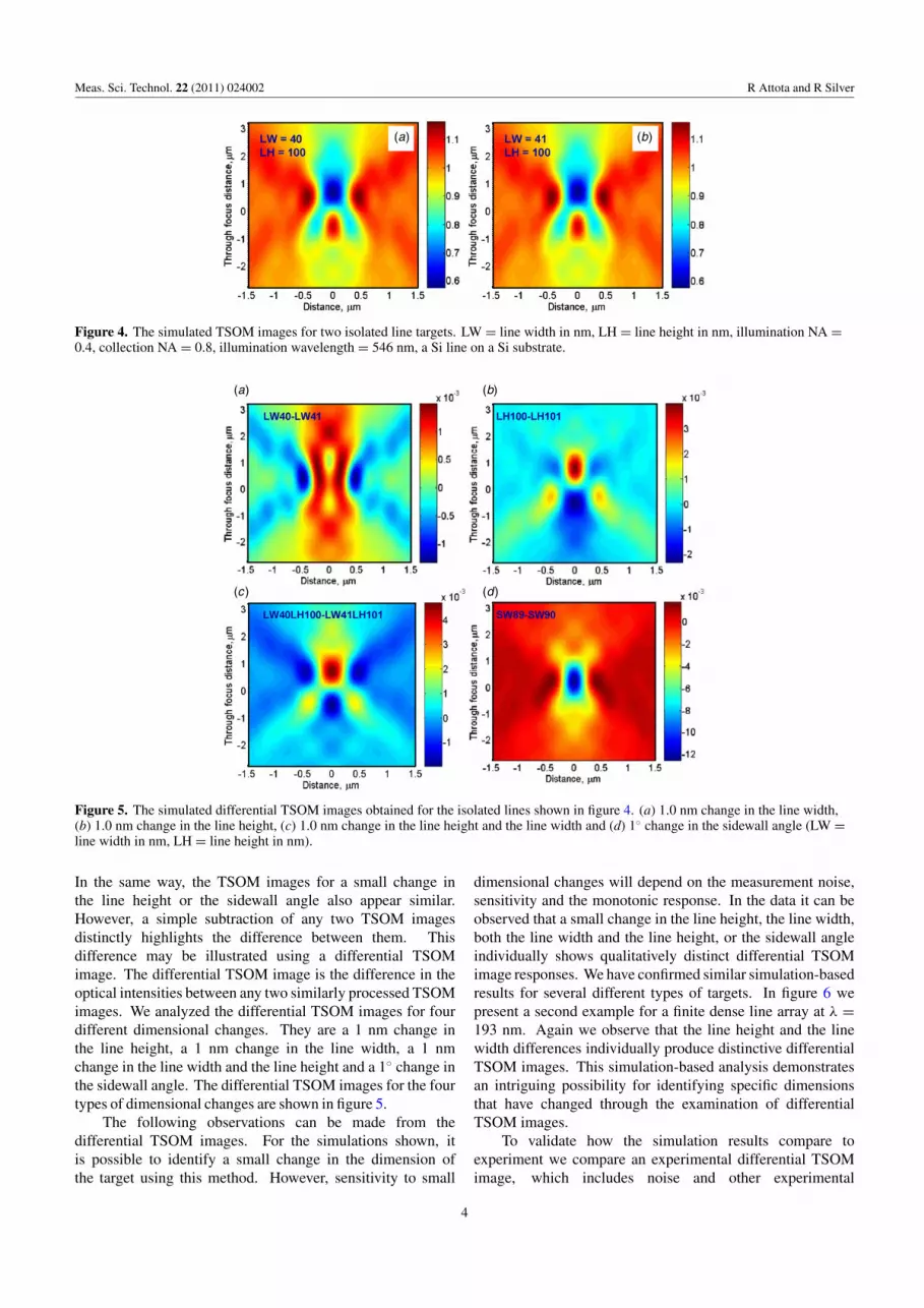
Although this method can be applied to any of thetargets discussed in this paper, in the current analysis wedemonstrate the approach for an isolated line (i.e. a line severalwavelengths away from nearby features). The TSOM imageswere simulated for small changes in the target dimensions.In figure 4 we present TSOM images for two targets with a1.0 nm difference in the line width. Visual inspection ofthe two TSOM images would indicate that they are similar.
3
Meas. Sci. Technol. 22 (2011) 024002 R Attota and R Silver
(a) (b)
Figure 4. The simulated TSOM images for two isolated line targets. LW = line width in nm, LH = line height in nm, illumination NA =0.4, collection NA = 0.8, illumination wavelength = 546 nm, a Si line on a Si substrate.
(a) (b)
(c ) (d)
Figure 5. The simulated differential TSOM images obtained for the isolated lines shown in figure 4. (a) 1.0 nm change in the line width,(b) 1.0 nm change in the line height, (c) 1.0 nm change in the line height and the line width and (d) 1◦ change in the sidewall angle (LW =line width in nm, LH = line height in nm).
In the same way, the TSOM images for a small change inthe line height or the sidewall angle also appear similar.However, a simple subtraction of any two TSOM imagesdistinctly highlights the difference between them. Thisdifference may be illustrated using a differential TSOMimage. The differential TSOM image is the difference in theoptical intensities between any two similarly processed TSOMimages. We analyzed the differential TSOM images for fourdifferent dimensional changes. They are a 1 nm change inthe line height, a 1 nm change in the line width, a 1 nmchange in the line width and the line height and a 1◦ change inthe sidewall angle. The differential TSOM images for the fourtypes of dimensional changes are shown in figure 5.
The following observations can be made from thedifferential TSOM images. For the simulations shown, itis possible to identify a small change in the dimension ofthe target using this method. However, sensitivity to small
dimensional changes will depend on the measurement noise,sensitivity and the monotonic response. In the data it can beobserved that a small change in the line height, the line width,both the line width and the line height, or the sidewall angleindividually shows qualitatively distinct differential TSOMimage responses. We have confirmed similar simulation-basedresults for several different types of targets. In figure 6 wepresent a second example for a finite dense line array at λ =193 nm. Again we observe that the line height and the linewidth differences individually produce distinctive differentialTSOM images. This simulation-based analysis demonstratesan intriguing possibility for identifying specific dimensionsthat have changed through the examination of differentialTSOM images.
To validate how the simulation results compare toexperiment we compare an experimental differential TSOMimage, which includes noise and other experimental
4

Meas. Sci. Technol. 22 (2011) 024002 R Attota and R Silver
(a) (b)
Figure 6. The simulated differential TSOM images obtained for finite dense arrays for (a) 2.0 nm change in the line height and(b) 2.0 nm change in the line width. Line width = 35 nm, line height = 100 nm, illumination NA = 0.3, collection NA = 0.8, illuminationwavelength = 193 nm, a Si line on a Si substrate.
(a) (b)
Figure 7. Comparison of (a) the simulation and (b) the experimental differential TSOM images. The differential images were obtained forthe two targets with line widths of 146 nm and 149 nm. Line height = 230 nm, pitch = 601 nm, illumination NA = 0.36, collection NA =0.8, illumination wavelength = 546 nm, a Si line on a Si substrate.
imperfections, with the simulation analysis. We chose twoline gratings (pitch = 601 nm) with 146 nm and 149 nmline widths (about 3 nm difference). Using λ = 546 nmlight, we obtained two experimental TSOM images that yieldone differential TSOM image. The process of obtainingthe experimental differential TSOM image requires someexplanation; we normalize the intensities of the experimentalTSOM images such that the maximum intensity in the imageis equal to 1 and the minimum intensity is equal to zero. Thetwo normalized TSOM images are then cross-correlated to getthe best match. At this point differential TSOM images areobtained. We applied the same normalization procedure to thesimulation results to maintain consistency with the experiment.Differential TSOM images from the simulations and theexperiments are shown in figure 7. Although agreement is farfrom ideal, the experimental and simulated differential TSOMimages have substantial qualitative similarities.
As shown above, different dimensional changes (i.e. widthor height) produce qualitatively distinct differential TSOMimages. However, for different magnitude changes of the samedimension, the differential TSOM images appear qualitativelysimilar. In figures 8(a) and (b) we present the differentialTSOM images for 2.0 nm and 4.0 nm differences in line width,respectively, for an isolated line. Similarly, we present thedifferential TSOM images for 2.0 nm and 4.0 nm differencesin the line heights in figures 9(a) and (b), respectively, foran isolated line. These simulations yield qualitatively similarappearing differential TSOM images. We performed a similaranalysis for several different types of targets under different
conditions. In all the cases tested we observed a similarbehavior. This behavior holds true as long as the difference inthe dimensional magnitude is small compared to the dimensionof the target. It is also important to note that the qualitativedifferences in the differential TSOM images for variousdimensional changes (e.g. line width versus line height) aremuch stronger than compared with the differences observedin the differential TSOM images for various magnitudes ofchange in the same dimensional parameter (1 nm versus 2 nmline widths).
To quantify the magnitude of the difference for a singleparameter, we evaluate the ‘mean square difference’ (MSD),which is defined here as
MSD = 1
n
n∑
i=1
(TSOM image1 − TSOM image2)2,
where n is the total number of pixels in the image. 1.0and 2.0 nm differences in the line widths of an isolated line(figure 8) produce the MSD values of 0.58 × 10⁻⁶ and2.45 × 10−6, respectively. Similarly, 1.0 and 4.0 nmdifferences in the line heights, as shown in figure 9, producethe MSD values of 0.38 × 10⁻⁶ and 1.56 × 10⁻⁶, respectively.In these two examples, the MSD values increased in directrelationship to the magnitude of the dimensional differences.However, the amount of increase depends on the individualcase. For consistent results and comparison, the total numberof points in the images, the selected X-axis distance and thefocus range must be kept constant.
5

Meas. Sci. Technol. 22 (2011) 024002 R Attota and R Silver
(a) (b)
Figure 8. The simulated differential TSOM image obtained for (a) the line widths of 102 nm and 100 nm (2.0 nm difference) and (b) theline widths of 104 nm and 100 nm (4.0 nm difference). Isolated line, line height = 100 nm, illumination NA = 0.25, collection NA = 0.95,illumination wavelength = 546 nm, a Si line on a Si substrate.
(a) (b)
Figure 9. The simulated differential TSOM image obtained for (a) line heights 102 nm and 100 nm (2.0 nm difference) and (b) line heights104 nm and 100 nm (4.0 nm difference). Isolated line, line width = 100 nm, illumination NA = 0.25, collection NA = 0.95, illuminationwavelength = 546 nm, a Si line on a Si substrate.
3.2. Determination of the absolute dimension of a target
The utility of the TSOM image approach in metrology isbased on an assumption that any given target produces aunique TSOM image under a given experimental condition. Apreliminary test to study the uniqueness of the TSOM imageusing simulations found the assumption to be satisfactory [8].
We now apply the same technique to experimentallymeasure the line width of the line grating target shown infigure 3(b). These results are preliminary in nature. Weevaluated the dimensions of the selected target, including theline width, using reference metrology tool such as an AFM.The AFM-measured line width was 145 nm for the selectedtarget. However, in the analysis here we assumed the linewidth to be ‘unknown’. Using the measured dimensions wesimulated a small library of TSOM images by keeping theline height (230 nm), the pitch (601 nm) and the sidewallangle (which is curved) constant. For the simulation ofthe library, we varied only the line width from 140 nmto 160 nm with a step increment of 0.5 nm. The librarymatching of the experimental TSOM image (figure 3(b)) wascarried out by evaluating the MSD values from the differentialTSOM images. The differential TSOM images between theexperimental and the simulated TSOM images were obtainedafter they were aligned to get the best match. A plot of theMSD values thus evaluated as a function of the line width inthe library is shown in figure 10. The inset shows a magnifiedview of the minimum of the curve. This gives the best linewidth match as 153 nm. The TSOM image-based line widthvalue differs with the AFM-measured line width of 145 nm.
Figure 10. A plot of the MSD values evaluated comparing theexperimental ‘unknown’ target with the library of simulations. Theinset shows the magnified portion of the highlighted curve.
The discrepancy between the AFM and the optical techniqueused here requires further study and is beyond the scope ofthe current paper. However, this example demonstrates thepotential utility of the TSOM method for absolute dimensionalmeasurements.
4. Optimization
The sensitivity of a given measurement can be enhancedby optimizing experimental parameters such as polarization,wavelength, illumination and collection numerical apertures.
6

Meas. Sci. Technol. 22 (2011) 024002 R Attota and R Silver
The polarization state of the illumination produces differentsensitivities for a given dimensional difference. This isillustrated in [8] for an isolated line at λ = 193 nm and100 nm nominal line height for unpolarized, TE-polarized(electric field pointing along the lines) and TM-polarized(electric field pointing perpendicular to the lines) illumination.The results show a large difference in the MSD value(i.e. sensitivity) depending on the illumination polarizationfor a 2.0 nm difference in the line height. Under thegiven simulation conditions, the TM polarization producedmaximum sensitivity, about ten times the sensitivity comparedwith that of unpolarized light. Similarly one can optimizethe experimental conditions such as illumination numericalaperture (NA) or collection NA to produce the maximumsensitivity [8].
5. Robustness to optical aberrations and processvariations
For metrology applications it is important to evaluate therobustness of the differential TSOM image method. All opticaltools have a degree of optical aberration. It is importantto know the degree to which error is introduced in themeasurement due to the presence of optical aberration. Westudied this using simulations for the overlay measurementof an in-chip overlay target [11]. The TSOM imageswere simulated under two conditions: without opticalaberration and with third-order spherical aberration (withthe Zernike coefficient of 0.01). The optical intensitysimulated with the programmed spherical aberration exhibiteda considerable difference compared with the aberration-freeprofile. However, the evaluated MSD under the two conditionsto measure the overlay showed a very small variation of about0.0004 nm for a 4 nm overlay. The error in the overlaymeasurement is negligible under the experimental conditionsindicating that this method is robust to optical aberration aslong as the aberration remains constant between the comparedTSOM images.
In practice, it is common to have process variations thatproduce small changes in the dimensions of the metrologytargets, including overlay measurement targets [11]. Fora 4 nm overlay the selected target in [11] produced theMSD value of 21.7 × 10⁻⁶. A 5 nm change in the lineheight due to process variations produced the MSD value of22.3 × 10−6, which results in a 0.06 nm error in the overlaymeasurement. Similarly a 4 nm difference in the line widthproduced an overlay error of 0.032 nm. This example showsa relatively small error in the overlay measurement due toprocess variations, and hence makes this method robust forthe example conditions studied in [11].
6. Optical models
For most of the simulation work presented here, a finitedifference time domain (FDTD) optical model was used [5].This model is capable of simulating 3D targets. On a limitedbasis a second, rigorous couple waveguide analysis (RCWA)optical model [4] was employed. The RCWA model is
capable of simulating only 2D targets. 3D optical modelingis computationally intensive, and depending on the size ofthe simulation domain, grid size and accuracy required, a 3Dsimulation with FDTD model can take as little as a few hours toseveral days using a high-end desktop computer. The opticalmodels used here have been thoroughly studied and comparedin house to evaluate their accuracy.
In the current work, for the process-control-typeapplications, optical modeling may not be required asthe method relies on differential TSOM imaging. However, theaccuracy of the optical simulations is of paramount importancefor the second type of application where an experimentalTSOM image is compared with a library of simulations.A thorough quantification of the optical microscope suchas illumination NA, collection NA, satisfactory Kohlerillumination and uniformity of illumination across the fieldof view is also needed for this application. In addition, theoptical constants of the target materials need to be determinedprecisely.
7. Some example applications
We highlight here some of the several applications that arepossible with the TSOM imaging method.
7.1. Dimensional analysis of nanoparticles
In principle, the size and shape of nanoparticles can beanalyzed using the TSOM method. Here we examine thisapplication using simulations. First we present particle sizeanalysis using the library-matching method. A typical TSOMimage of a gold nanoparticle (60 nm) is shown in figure 1(b).The TSOM images for different sized nanoparticles changewith size. We make use of this difference to determine thenanoparticle size. The first step for this is the simulationof a library of TSOM images for various sizes within theexpected size range. In the second step we acquire theexperimental TSOM images of the nanoparticle needingsize determination. The third step is to compare the TSOMimage of the nanoparticle of unknown size with that of thelibrary to determine the MSD values of the differential images.A plot of the MSD values thus obtained is shown in figure 11.If the size of the unknown particle is within the size range ofthe library, in principle, the plot shows a well-defined minima.The size corresponding to the minima indicates the size of theunknown particle. In this example, an ‘unknown’ nanoparticlesize of 69.5 nm produced the best-match size of 69.45 nm. Animproved method is to create the library with the experimentalTSOM images of the particles with pre-determined sizes. Thisnearly eliminates the issues arising due to mismatch betweenthe simulated and the experimental TSOM images.
As presented in the above sections, one importantcharacteristic of TSOM imaging is the ability to differentiatedifferent dimensional changes. This is also applicable tonanoparticle analysis. We present here differential TSOMimages for size and shape differences of nanoparticles.Figure 12(a) shows a differential TSOM image for a 2 nmdifference in the size (diameter). Compare this with the
7

Meas. Sci. Technol. 22 (2011) 024002 R Attota and R Silver
Figure 11. Determination of unknown particle diameter using thebest-match method from a library of simulations. Library range:60 nm to 80 nm. Best-match diameter: 69.45 nm. IlluminationNA = 0.3, collection NA = 0.95, illumination wavelength =365 nm, a gold particle on a quartz substrate.
differential TSOM image shown in figure 12(b) for a differencein the shape (ellipsoid to sphere). We can see that sizedifference has a distinct differential image compared withshape difference.
7.2. Defect analysis in gratings
Under certain circumstances a direct observation of the TSOMimage is helpful. For example, the TSOM images can highlightthe presence of defects and the type of defect in a dense grating.As a demonstration we present experimental TSOM images forsix dense gratings (nominal pitch = 200 nm and nominal linewidth = 100 nm) fabricated with intentional defects as shownin figure 13. The six types of defects with 10 nm differencesin the line widths produce distinctly different TSOM images,firstly indicating the presence of defects and secondly pointingto the type of defect. In contrast, the absence of defects wouldproduce featureless TSOM images for these dense targets.This type of analysis is also applicable to isolated line defectsin an array of lines as shown in figure 14 for 2 nm reductionin the line width, or several random defects present in a densegrating.
(a) (b)
Figure 12. Simulated differential TSOM images for (a) the size difference of 2.0 nm in diameter (62.0 nm and 60.0 nm) and (b) the shapedifference as a result of 5.0 nm elongation in the height. Illumination NA = 0.3, collection NA = 0.95, illumination wavelength = 365 nm,a gold particle on a quartz substrate.
7.3. Overlay analysis
Target-specific overlay applications are demonstrated usingsimulation results at an illumination wavelength of 193 nm.The target is a finite dense array with nine lines. We present ananalysis for an overlay offset of 2.0 nm of each alternate line.The differential TSOM image obtained using the base target(zero overlay offset) and the target with a 2.0 nm offset is shownin figure 15. The differential TSOM image shows good signalstrength and sensitivity for a 2.0 nm overlay. A line is drawnin the differential TSOM image to indicate the center of thetarget. Positive or negative overlay values may be identified byanalyzing the symmetry of the differential TSOM image aboutthis center line. This type of target analysis has applicationsin double patterning lithography. For more information onapplication of the TSOM method for overlay analysis refer to[8] and [11].
8. Summary
This paper presents an initial review of a novel techniquewhich uses the additional information contained in a setof through-focus optical images as compared with a singleimage at the best focus position. The two-dimensional TSOMmethod was used to analyze dimensional information of sub-100 nm targets. The TSOM images are formed by stackingthe through-focus optical image intensity profiles such thatthe X-axis represents the lateral distance on the target, the Y-axis represents the through-focus position and the intensityof the image (the Z-axis) represents the optical intensity.We proposed two main applications of the TSOM images:(i) determination of a change in the relative dimension and(ii) determination of the absolute dimensions of a target. Wepresented several examples using the optical simulations andthe experimental results.
Differential TSOM images are generally distinct fordifferent parametric changes. They enable us to identify whichparameter is different between the two targets. However, thedifferential TSOM images obtained for different magnitudechanges of the same parameter appear qualitatively similar.In this case, the MSD value enables us to determinethe magnitude of the difference in the dimension. TheTSOM images enable us to determine the dimensions of an
8

Meas. Sci. Technol. 22 (2011) 024002 R Attota and R Silver
(a) (b) (c )
(d ) (e) (f )
Figure 13. Experimental TSOM images for dense line gratings fabricated with intentional defects. Every (a) tenth, (b) fifth and (c) thirdline is smaller by 10 nm. Every (d) tenth, (e) fifth and (f ) third line is larger by 10 nm. Illumination wavelength = 546 nm, nominal linewidth = 100 nm, nominal pitch = 200 nm, illumination NA = 0.36, imaging NA = 0.8.
Figure 14. The differential TSOM image showing the presence of asingle line defect that is 2 nm smaller then the other line widths in adense finite grating. LW = 35 nm, LH = 100 nm, pitch = 105 nm,illumination NA = 0.3, collection NA = 0.8, total number of linessimulated = 9, illumination wavelength = 193 nm, a Si line on a Sisubstrate.
unknown target by the library-matching method, provided wehave accurate simulations and experimental results for a fullycharacterized optical microscope. Potential applications of theTSOM method include defect analysis, inspection and processcontrol, critical dimension (CD) metrology, photomask
Figure 15. The differential TSOM image application for doublepatterning overlay analysis showing an overlay offset of 2 nm forfinite dense array. LW = 35 nm, LH = 100 nm, pitch = 105 nm,illumination NA = 0.3, collection NA = 0.8, total number of linessimulated = 9, illumination wavelength = 193 nm, a Si line on a Sisubstrate.
metrology, overlay registration metrology, nanoparticlemetrology, film thickness metrology, 3D interconnectmetrology (large range depth analysis such as TSVs) andline-edge roughness measurement. Numerous industries couldbenefit from the TSOM method—such as the semiconductor
9

Meas. Sci. Technol. 22 (2011) 024002 R Attota and R Silver
industry, MEMS, NEMS, biotechnology, nanomanufacturing,nanometrology and photonics. The method is relativelysimple, inexpensive, has high throughput, provides nanoscalesensitivity for 3D measurements and potentially saves millionsof dollars for nano/microscale metrology and manufacturing.Future work includes extending the current method to three-dimensional targets and analyzing the full 3D TSOM imagespace.
Acknowledgments
The NIST Office of Microelectronics Programs is gratefullyacknowledged for financial support as well as the NISTScatterfield Competence project. The authors thank Sematechfor wafer fabrication and measurement support, and JamesPotzick, Thomas Germer, John Kramar, Michael Stocker,Bryan Barnes, Yeung Joon Sohn and Richard Quintanilha fortheir direct or indirect assistance.
References
[1] National Science and Technology Council (NSTC)/NanoscaleScience, Engineering, and Technology (NSET) 2004Instrumentation and metrology for nanotechnology Reportof the National Nanotechnology Initiative Workshophttp://www.nano.gov/NNI_Instrumentation_Metrology_rpt.pdf
[2] Lojkowski W, Turan R, Proykova A and Daniszewska A 2006Nanometrology: Eighth Nanoforum Reporthttp://www.nano.org.uk/members/MembersReports/NANOMETROLOGY_Report.pdf
[3] Schwenke H, Neuschaefer-Rube U, Pfeifer T andKunzmann H 2002 Optical methods for dimensionalmetrology in production engineering Ann. CIRP 51 685–98
[4] Davidson M 1991 Analytic waveguide solutions and thecoherence probe microscope Microelectron. Eng.13 523–6
[5] Pistor T V 2001 Electromagnetic simulation and modelingwith applications in lithography PhD Thesis MemorandumNo UCB/ERL M01/19
[6] Germer T A and Marx E 2006 Simulations of opticalmicroscope images Proc. SPIE 6152 61520I
[7] Attota R, Silver R M and Potzick J 2006 Optical illuminationand critical dimension analysis using the through-focusfocus metric Proc. SPIE 6289 62890Q
[8] Attota R, Silver R M and Barnes B M 2008 Opticalthrough-focus technique that differentiates small changes inline width, line height, and sidewall angle for CD, overlay,and defect metrology applications Proc. SPIE6922 69220E
[9] National Institute of Standards and Technology 2008Nanoscale dimensioning is fast, cheap with new NISToptical technique NIST Tech Beat 28 October http://www.nist.gov/public_affairs/techbeat/tb2008_1028.htm#tsom
[10] Attota R, Germer T A and Silver R M 2008 Through-focusscanning-optical-microscope imaging method fornanoscale dimensional analysis Opt. Lett.33 1990–2
[11] Attota R et al 2009 Through-focus scanning and scatterfieldoptical methods for advanced overlay target analysis Proc.SPIE 7272 727214
[12] Attota R, Germer T A and Silver R M 2009 Nanoscalemeasurements with a through-focus scanning opticalmicroscope Future Fab Int. 30 83–8
[13] Announcement of 2010 R&D 100 Award for the TSOM method,http://www.rdmag.com/Awards/RD-100-Awards/2010/07/R-D-100-2010-Winners-Overview
[14] Press release from NIST about 2010 R&D 100 Award for theTSOM method, http://www.nist.gov/public_affairs/tech-beat/tb20100721.cfm#nanoscale
[15] Salata O V 2004 Applications of nanoparticles in biology andmedicine J. Nanobiotechnol. 2 3
10