multiplexing phototransistor arrays using transistor ... - core
TRANSCRIPT
University of Central Florida University of Central Florida
STARS STARS
Retrospective Theses and Dissertations
1986
Multiplexing Phototransistor Arrays Using Transistor Capacitance Multiplexing Phototransistor Arrays Using Transistor Capacitance
Gary E. Morrissette University of Central Florida
Part of the Engineering Commons
Find similar works at: https://stars.library.ucf.edu/rtd
University of Central Florida Libraries http://library.ucf.edu
This Masters Thesis (Open Access) is brought to you for free and open access by STARS. It has been accepted for
inclusion in Retrospective Theses and Dissertations by an authorized administrator of STARS. For more information,
please contact [email protected].
STARS Citation STARS Citation Morrissette, Gary E., "Multiplexing Phototransistor Arrays Using Transistor Capacitance" (1986). Retrospective Theses and Dissertations. 4970. https://stars.library.ucf.edu/rtd/4970

MULTIPLEXING PHOTOTRANSISTOR ARRAYS USING TRANSISTOR CAPACITANCE
BY
GARY E. MORRISSETTE B.S.E., University of Central Florida, 1985
THESIS
Submitted in partial fulfillment of the requirements for the degree of Master of Science in Engineering in the
Graduate Studies Program of the College of Engineering University of Central Florida
Orlando, Florida
Fall Term 1986
ABSTRACT
Photodetector Focal Plane Arrays are used in
electronic image detection. This paper examines the
multiplexer that converts the detected signals to a Time
Division Multiplexed form. This paper will present two types
of multiplexers, a traditional linear multiplexer and a
matrix addressed multiplexer. These arrays will use the
concept of charge storage to amplify the detected signal.
The capacitance of the junctions of phototransistors are
used for charge storage.

ACKNOWLEDGEMENTS
The author wishes to thank Dr. Martin for his support
in the research of this thesis and for his assistance
throughout my graduate program. In addition, I would like to
thank the committee for their reveiw of this paper and Dr.
Brown for his help in measurement of the 4N25 optocouple.
Finally, I would like to thank my family whose support
thoughout my college education was most appreciated.
iii

TABLE OF CONTENTS
LIST OF TABLES . . . . . . . . . . . . . . vi
LIST OF FIGURES vii
LIST OF SYMBOLS ix
INTRODUCTION Focal Plane Arrays . . . . • . . . • .
1 1 3 4
A Simple Model . . . . . . . . . . . . . . . . Characterization of the 4N25 Optocoupler . . . . .
BACKGROUND INFORMATION • . • . . . • . . • . . . . . . 10 Diode Characteristics . • . . . . . . . . . . 10
Photovoltaic Operation . . . . . . ... 12 Charge Storage Operation . . • . . • . . • . 13
Phototransistor Characteristics . . . • • . . . . 15 Continuous Mode . . . . . . . 16 Charge Storage Mode . . . . • . . . . 17
Comparison of Photodiodes and Phototransistors . . 18 Common Detector Arrays . . . . . . . . . . . 19
DESIGN OF A SHIFT-REGISTER LINEAR ARRAY . • . . . • 21 Basic Cell . . . . . . . . . . . . • . • • . 21 Multiplexing Cells . . . . . . . . . . • . • . . . 25 Reduction of the Design to one switch per detector 30 Predicted Performance • • . • • • . . 33
MATRIX DESIGN . . . . . • . Basic Cell . . . . . . Multiplexed Array . . . Predicted Performance
• • • • • • • • • • • • • 34 • • • • • • • • • • • • • 34
• • • • • • • • • 3 7 • • • • • • • • • • • • 37
DATA . . . . . . . . . . . . . . . . . . • • • . 39 Shift-Register Linear Array . . . . . . . . . 39
D.C. Signal versus sample frequency ..... 39 Frequency Respons~ . . . . . . . . . . . 44
Matrix Addressed Array . . . . . . . . . . . . . 50 D.C, Signal versus sample frequency ••... 50 Frequency Response . . . . . . . . . . . 54
CONCLUSION . 58
iv

APPENDIX A DEVICE PIN DIAGRAMS . • • • 59
APPENDIX B SCHEMATICS • • • 62
APPENDIX C OPTOCOUPLER PLOTS • • • 65
APPENDIX D PICTURES • • • • 7 5
REFERENCES • • • • • 7 6
v

LIST OF TABLES
I. OPTOCOUPLER DATA . . . . . . . . . . . . . . 8
II. D.C. RESPONSE DATA FOR LINEAR ARRAY POSITION SEVEN 41
III. D.C. RESPONSE DATA FOR LINEAR ARRAY POSITION ONE . 42
IV. FREQUENCY RESPONSE DATA FOR LINEAR ARRAY . . . . 47
v. D.C. RESPONSE DATA FOR MATRIX ARRAY . . . 52
VI. FREQUENCY RESPONSE DATA FOR MATRIX ARRAY . . . 55
vi

LIST OF FIGURES
Optocoupler Measurement Setup . Plot Of ID Versus IC . . . . . . . . . Plot Of IB Versus IC . . . . . . . . . Plot Of Ip Versus IC . . . . . . . . .
1.
2.
3.
4.
5.
6.
Energy-Band Diagram Of A P-N Junction .
Typical Photodiode Curve
7. Diode Charge Storage Model
8. A Simple Phototransistor Model
9. Phototransistor Charge Storage Model
10. Phototransistor Charge Storage Model
11. Phototransistor During Integration
12. Transistor Diode Model
. .
. .
. .
. .
13. Block Diagram of Double Switch Linear Array
. . .
. . .
. . .
. . .
. . 4
. . 6
7
9
10
. • 13
. 14
. 15
. . 17
• 21
• • 2 3
• • 24
• • 26
14. Timing Diagram for Double Switch Linear Array . • 26
15. Schematic .for Double Switch Linear
16. Basic Cell for Single Switch Linear Array
17. Block Diagram for Single Switch Linear Array
18. Schematic for Single Switch Linear Array
19. Phototransistor Charge Storage Model
20. Phototransistor During Integration Period
21. Diode Model of Phototransistor
22. Schematic for Matrix Addressed Array
vii
• 27
30
. 31
• 32
• 34
• • • • • 36
• • • 3 6
• 38

23. D.C. Response Plot for Linear Array • • 4 3
24. Sample and Hold Circuit for Single Switched Array .. 45
25. Light Emitting Diode Driver Circuit ...
26. Frequency Response Plot for Linear Array
27. D.C. Response Plot For Matrix Circuit •.
28. Frequency Response Plot for Matrix Array
viii
. 46
. 48
• • • 53
• • • • 56

n
q
h
Io
Id
hf e
CBC
CBE
vcc v
0(t)
VBC
VBE
TO
LIST OF SYMBOLS
Diode Current
Transistor Base Current
Transistor Collector Current
Transistor Emitter Current
Photodiode Current
Quantum Efficiency
Charge on an Electron = 1.602E-19 Coulombs
Incident Radiant Flux Density
Area of the Photovoltaic Device
Speed of Light = 3E+8 Meters per Second
Planck's constant = 6.6E-34 Watt-sec2
Reverse Saturation Current
Dark Current
Transistor Current gain
Collector-Base Junction Capacitance
Base-Emitter Junction Capacitance
Power Supply Biased Voltage
Circuit Output Voltage
Base-Collector Voltage
Base-Emitter Voltage
Integration period
ix

INTRODUCTION
Focal Plane Arrays
The purpose of this paper is to examine and compare two
schemes for time division multiplexing of focal plane
arrays. These two schemes are the traditional linear
multiplexer and the array multiplexer. The ideal
multiplexers for focal plane arrays should be programmable
and expandable. Each of the time division multiplexers
studied here has these desirable features.
The main use of focal plane arrays is image detection.
An array can be scanned in the X and Y directions and with
appropriate signal-processing techniques can be used to
produce an image. This has been done with CCD cameras which
produce excellent image quality, are small and light in
weight. They also permit direct recording onto video tape.
These arrays using infrared detectors could also be used to
track the position of a heat source [1].
2
As an image detector the linear array has its limits;
itcan not create an image without an external scanner. There
are cases where a linear array would be prefe~able to an
area array. Many image-sensing applications may be
accomplished using linear arrays of photodetectors. The use
of a moving image with a fixed detector can. provide the
scan. This scanner motion could be a page of text being
swept across the detector, or a data card could be read in a
card reader. Area surveillance is also a valid use of focal
plane arrays. A different kind of motion is needed for
intrusion detection, this could be provided by installing
the linear array in a rotating drum. With proper clocking,
this scan technique could provide a 360 degree camera. For
conventional cameras a rotating prism
horizontal scan while the array would
scanned in the vertical dimension [2].
would provide the
be electronically
3
A Simple Model
This paper developes two circuit schemes that address
photodetectors. Creating the optics to couple an image to
the detector can be a measurement problem. The use of
optical couplers can eliminate this problem as the optics
are self contained and the input and output currents are
easily measured. The optical coupler uses a photoemitter and
a photodetector to transmit and receive data. This device
also becomes a convenient means of studying optical devices.
This optical coupled pair allows one to control the
intensity of the light incident on the phototransistor. The
device characteristics can be measured. This permits a fixed
point of reference in which to measure the circuit
performance.
The optocoupler used will be the 4N25. This device
uses a GaAs light emitting diode and a silicon
phototransistor. The 0.9E-6 meter wavelength of light ·
emission in GaAs is near the peak response of the silicon
photodetector [3]. This is a standard optical coupler with
reasonable speed and efficiency. This device is an industry
standard device which is generally available.
4
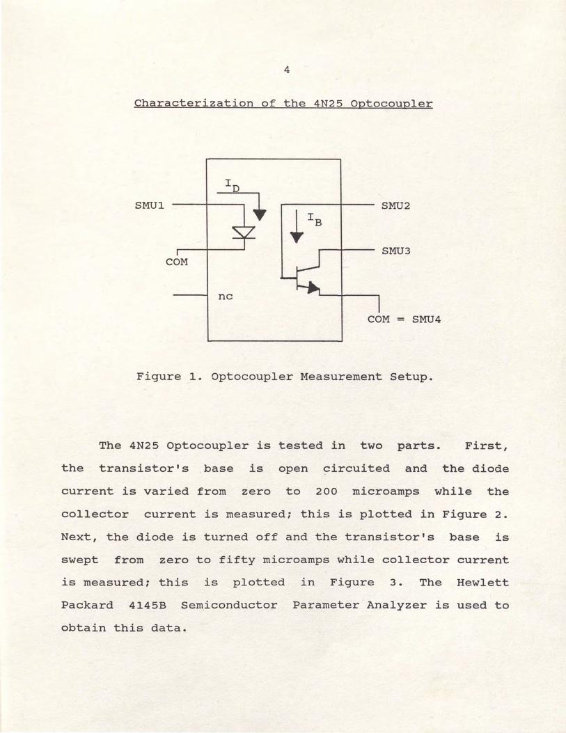
Characterization of the 4N25 Optocoupler
SMUl SMU2
SMU3 COM
COM = SMU4
Figure 1. Optocoupler Measurement Setup.
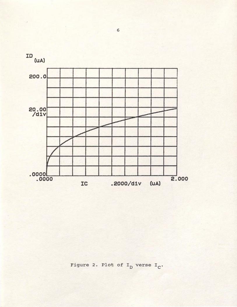
The 4N25 Optocoupler is tested in two parts. First,
the transistor's base is open circuited and the diode
current is varied from zero to 200 microamps while the
collector current is measured; this is plotted in Figure 2.
Next, the diode is turned off and the transistor's base is
swept from zero to fifty microamps while collector current
is measured; this is plotted in Figure 3. The Hewlett
Packard 4145B Semiconductor Parameter Analyzer is used to
obtain this data.

5
The model of the phototransistor used in this paper has
an ideal photodiode in parallel with a capacitor across the
base-collector junction of the transistor. The optocoupler
is used as both the light source and the detector. Since
the optocouple's base lead is not used then base current can
be modeled as the photodiode current (Ip)· This data is
used to generate a plot of IP as a function
data is in Table I, plotted in Figure
This
4, and used in
calculations of the photogenerated current IP when needed.
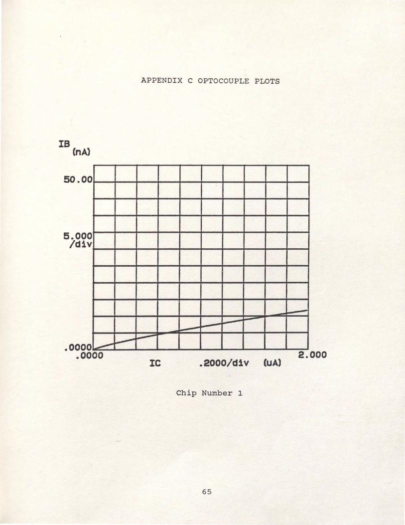
Five optocouplers were analyzed and their data is in
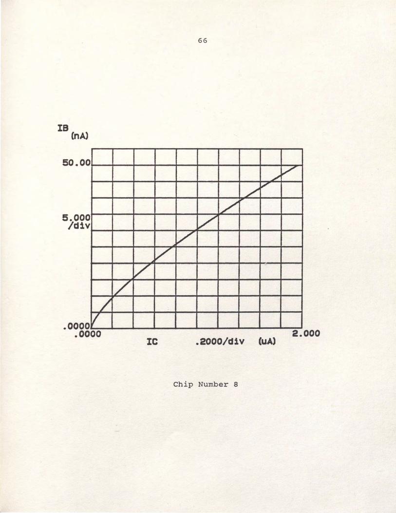
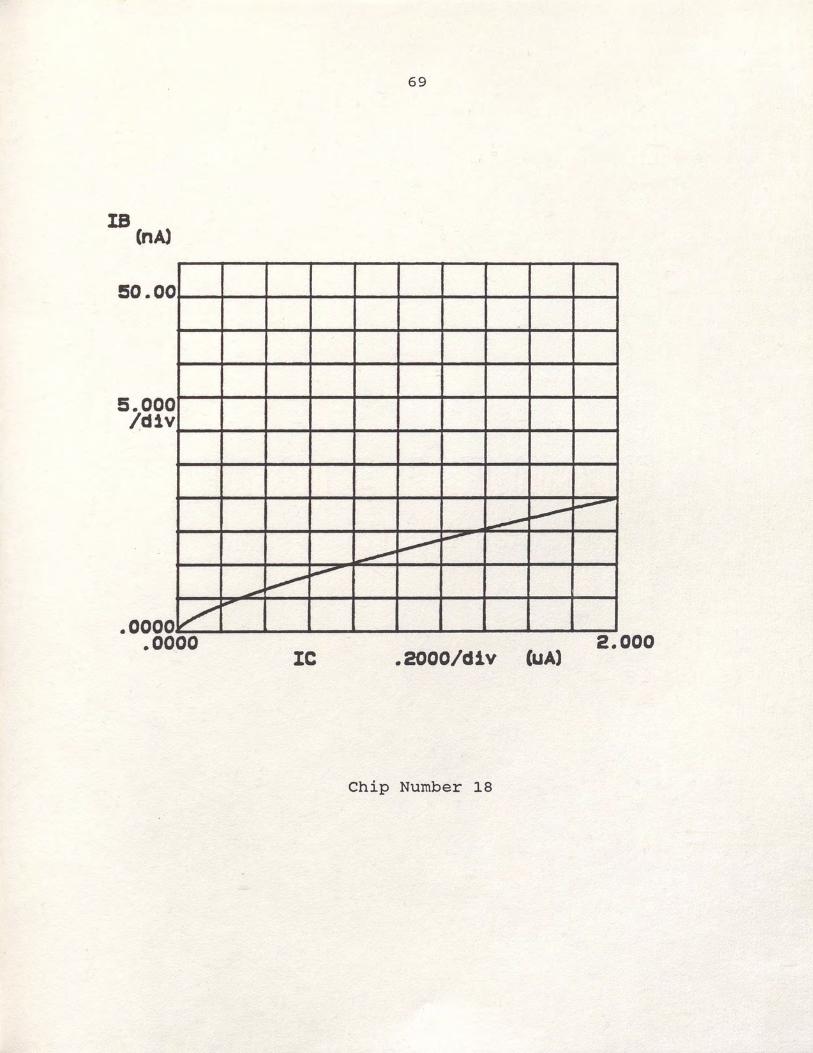
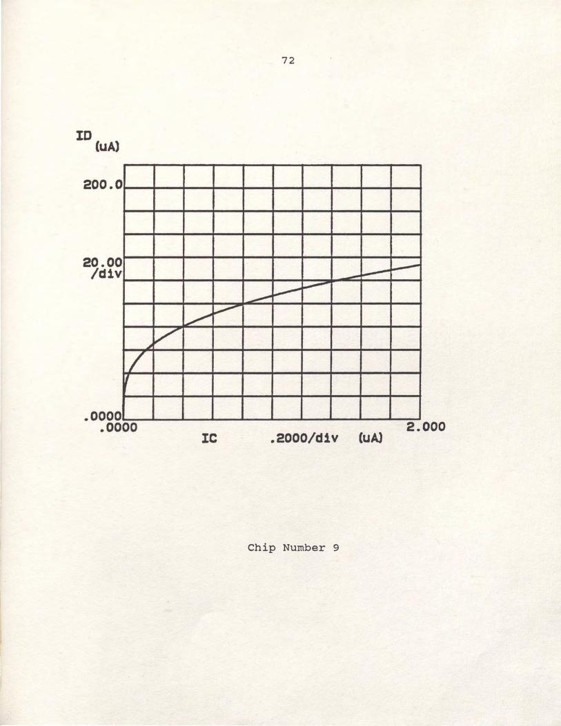
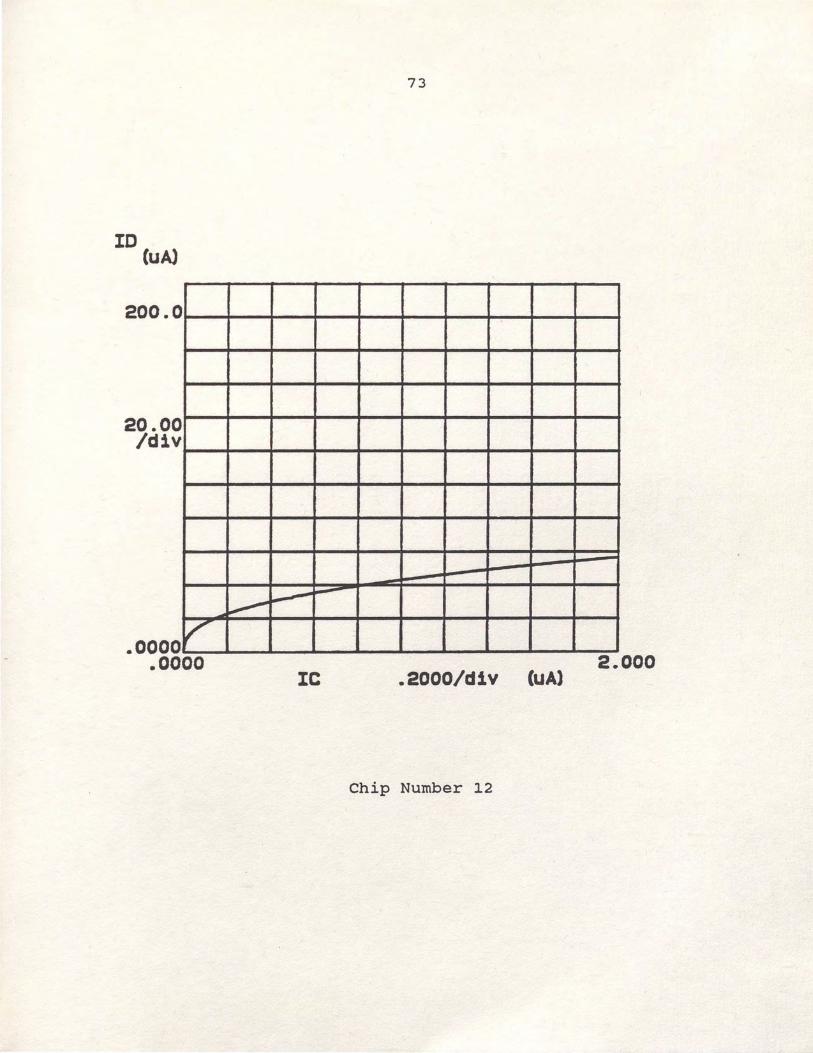
Appendix c. It is important to notice that the plots of I 0
versus IC and IB versus IC vary greatly. This is caused by
the variation in hfe for each phototransistor and the
coupling efficiency between the L.E.D. and the
phototransistor. This variation will cause a difference in
voltages between pulses in the circuit's output.
ID (uA)
200.0
20.00 /div
/ (
.0000 .0000
6
------,_____.
~
~ ~
------~ ~
v
2.000 IC .2000/div CuA)
Figure 2. Plot of r 0 verse IC.

IB CnAl
50.00
5.000 /div
/ .0000 .0000
/ ~
7
-~ ~
__,,,,
~ ---~
/ _,
~
_/ """" L
2.000 IC .2000/div (uA)
Figure 3. Plot of IB verse IC.

8
TABLE I
OPTOCOUPLER DATA
40 2.5
50 4
60 6
70 8
76 10
80 11
88 13
97 16
100 17
105 19
114 21.5
119 24
125 26
130 28
135 32
145 36
I · (E-6A) c
0.06
Ool
0.2
0.3
0.4
0.46
0.6
0.8
0.88
1.0
1.2
1.4
1.6
1.8
2.0
2.5

9
40
30
20
10
0
·o 25 50 75 100 125 150
I 0 (E-6 Amps)
. Figure 4. Plot of IP verse IC.

BACKGROUND INFORMATION
Diode Characteristics
The photovoltaic effect requires a potential barrier
with an electric field in order to operate. A P-N junction
is usually employed to obtain these conditions. Figure 5
illustrates the energy-band diagram of a P-N junction. Two
basic requirements for photovoltaic operation are that the
incident photons have sufficient energy to excite
photoelectrons across an energy gap and that the temperature
of the detector be low enough so that electrons are not
thermally excited across the bandgap [4].
E _...
~~~~~~~-e-l_e_~~t-r-o-~ E
t c
E g. E v he/\ .. ~
------ c;:::"f hoie
Figure 5. Energy-Band Diagram of A P-N Junction.
10
11
The upper limit to the wavelength at which the
photovoltaic effect will operate can be defined as:
Xmax = 1.24/E (2-1) g
where Eg is the junction energy gap in electron volts and A
is the wavelength in microns. A photodiode is capable of
detecting only radiation with photon energy greater than the
energy gap [4]. Silicon has a maximum wavelength of 1.1
microns and an energy gap of 1.12 electron volts. Germanium
has a maximum wavelength of 1.9 microns with an energy gap
of .65 electron volts.
12
Photovoltaic Operation
The total current in a photovoltaic P-N junction can be
defined as It = Id Ip where Id is the dark current in
amperes and given by
Id= I0
(exp(qVd/kT)-1) ( 2-2)
Ip is the photon-generated current and given by
( 2-3)
where n is the quantum efficiency, q is the charge on an
electron = 1.602E-19 Coulomb,
flux density (irradiance), Ad
E is the incident radiant e
is the area of the
photovoltaic device, C is the speed of light, h is Planck's
constant = 6.6E-34 Watt-sec2, Vd is the diode voltage in
volts and I0
is the reverse saturation current
characteristic of the device in amperes. The total current
can be given as [4]
( 2-4)
A typical Diode curve is shown in Figure 6.

13
Figure 6. Typical Photodiode Curve.
Charge Storage Operation
The image application for focal plane arrays uses P-N
photodiodes where the individual devices are sampled in a
periodic manner. If the photodiode is operated in the
photovoltaic mode, the active properties of the diode are
used only during the sampling time. A photon-flux
integration diode or storage mode diode allows the device to
be active 100 percent of the time [5]. Storage mode
operation is based on the fact that the rate of voltage
decay across an open-circuited reversed biased junction
depends on the magnitude of the incident photon flux.
14
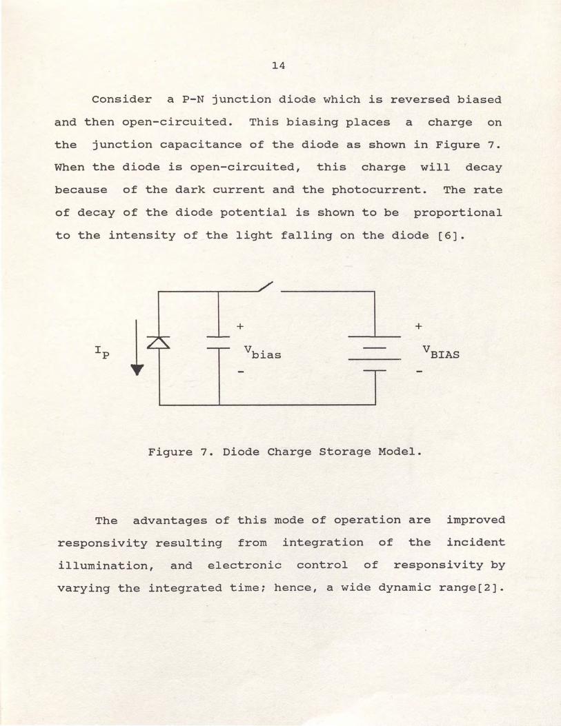
Consider a P-N junction diode which is reversed biased
and then open-circuited. This biasing places a charge on
the junction capacitance of the diode as shown in Figure 7.
When the diode is open-circuited, this charge will decay
because of the dark current and the photocurrent. The rate
of decay of the diode potential is shown to be proportional
to the intensity of the light falling on the diode [6].
+
vb. ias
+
.Figure 7. Diode Charge Storage Model.
The advantages of this mode of operation are improved
responsivity resulting from integration of the incident
illumination, and electronic control of responsivity by
varying the integrated time; hence, a wide dynamic range[2].
15
Phototransistor Characteristics
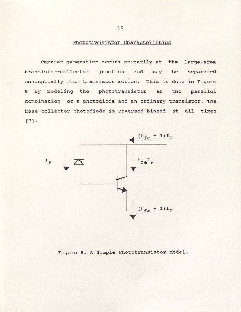
Carrier generation occurs primarily at the large-area
transistor-collector junction and may be separated
conceptually from transistor action. This is done in Figure
8 by modeling the phototransistor as the parallel
combination of a photodiode and an ordinary transistor. The
base-collector photodiode is reversed biased at all times
[7].
(hf + l)Ip ~ e
Figure 8. A -Simple Phototransistor Model.

16
Excess electron-hole pairs are continuously generated
on both sides of the collector-base photodiode. The excess
majority carriers stay in their corresponding side of the
junction. The excess minority carriers within one diffusion
length of the junction edge glide over to the opposite side
of the collector-base junction giving rise to the
photogenerated current Ip [8]. is in the collector to
base direction. The relationship of Ip to the quantum
efficiency n is the same as that for the photodiode, where
IP can be considered as the base current of the transistor.
(2-5)
I =(hf + 1)nqE Ad~ /he c e e (2-6)
This relationship shows that the phototransistor has an
effective quantum efficiency which is (hfe + 1) times that
of the collector-base photodiode [8].
Continuous Mode
The phototransistor can be used in the continuous mode
where the photon-ge~erated carriers in or near the base
region are beta multiplied, resulting in an output current
proportional to the instantaneous photon flux on the sensor.

17
There are several disadvantages with this mode of operation.
First, output current is highly dependent on the beta of the
transistor. Second, for low light levels the signal voltage
will be small and will require amplification before signal.
processing can be performed.
Charge Storage Mode
The phototransistor, by virtue of its current gain
offers the possibility for higher sensitivity than does a
simple photodiode. The junction capacitance provides the
charge storage. A charge is integrated over a period of time
to produce a voltage gain.
+
+
Figure 9. Phototransistor Charge Storage Model.
18
Comparison of Photodiodes and Phototransistors
The transistor has large beta variations which cause
the parameters to be less uniform between detectors in the
array, whereas the diode is more uniform. Since the diode
has one P-N junction, the processing and fabrication is
simple compared to the phototransistor which has two P-N
junctions. The phototransistor, with its current gain,
offers the possibility for higher sensitivity than does a
simple photodiode. Since the current gain of the transistor
varies with current, then the photogain is not constant and
the output current is not a linear function of the light
level incident on the photodetector. It would depend on the
requirement of the application to determine if the higher
sensitivity of the phototransistor outweighs the problems it
introduces over the diode.
19
Common Detector Arrays
Recent advances in charge-coupled device (CCD)
technology have lead to the development of high density self
scanned infrared detector arrays. There are basically two
types of infrared focal pl~nes, monolithic and hybrid [9].
Hybrid focal planes consist of coupling photodetectors
to a silicon CCD shift-register unit. The functions of
detection and signal processing are performed in distinct
components. The role of the silicon CCD is that of a signal
processor performing operations such as multiplexing and
amplification. These focal planes can be divided into two
sub-classes: direct and indirect injection devices. In
direct injection devices the photogenerated charge is
directly injected from the detector into the CCD. With
indirect injection devices a buffer stage exists between the
two components (10]. An advantage with Hybrid focal planes
is the use of detectors that give an optimum response over
the wavelength of interest. This technique also permits the
use of silicon which is the most common material in present
CCD technology. The main disadvantage with hybrid focal
planes comes with bonding the detector to the CCD which can
be a difficult process.

20
Monolithic focal planes have the multiplexer fabricated
as an integral part of the structure. For these devices
both the sensor and processor are built up on the same
semiconducting substrate.
elimination of connection
elements that make the
difficult make into a CCD.
An advantage of this is
problems. Unfortunately
most responsive sensor can
the
the
be
For the presented design, discrete elements will be
selected to build a segment of a focal plane array. Due to
part and device limitations this · array will contain a small
number of detectors and will be impedance and frequency
scaled to the discrete capacitance levels. These arrays can
be modified to accommodate a large number of detectors. In
order to implement the design presented in this paper with a
large array would require the use a CCD and one of the
techniques in the previous two paragraphs.
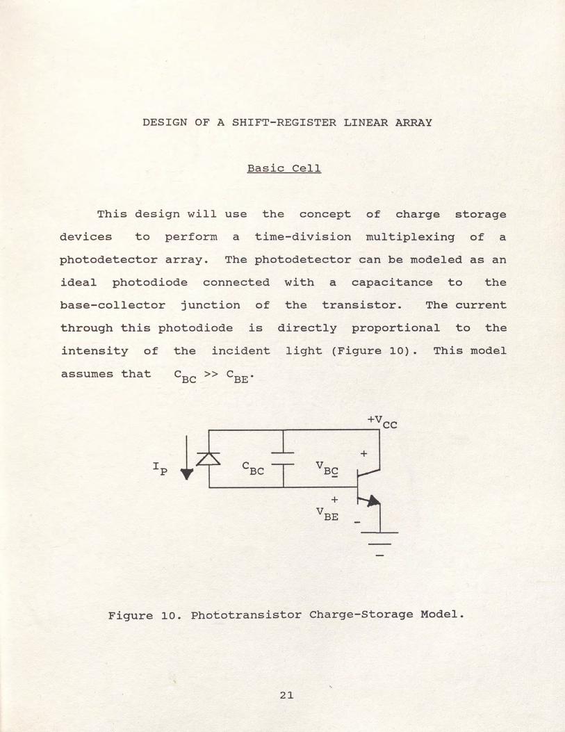
DESIGN OF A SHIFT-REGISTER LINEAR ARRAY
Basic Cell
This design will use the concept of charge storage
devices to perform a time-division multiplexing of a
photodetector array. The photodetector can be modeled as an
ideal photodiode connected with a capacitance to the
base-collector junction of the transistor. The current
through this photodiode is directly proportional to the
intensity of the incident light (Figure 10). This model
assumes that
Figure 10. Phototransistor Charge-Storage Model.
21

22
First, the base-collector junction capacitance is
charged by connecting the emitter lead to ground and the
collector lead to +Vee as shown in Figure 10. This places a
charge on CBC which results in a voltage potential.
{3-1)
At time t = o the emitter is open-circuited and IE and
VBE are equal to zero. This is shown in Figure 11 and
Figure 12. The base-collector diode is reversed-biased and
assuming negligible generation-recombination current, no
current flows though the base-emitter junction. In the
base-collector junction, the photocurrent IP flows though
CBC and can be modeled during the discharge period.
With this equation IP can be assumed to be constant
with respect to time if the photodiode is operated in the
linear region and the sample frequency is an order of
magnitude greater than the signal frequency. Then equation
{3-2) maybe integrated to yield:
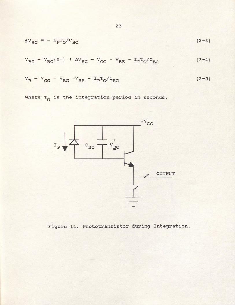
23
(3-3)
(3-4)
(3-5)
Where T0 is the integration period in seconds.
+vcc ------...-----..--
OUTPUT
Figure 11. Phototransistor during Integration.
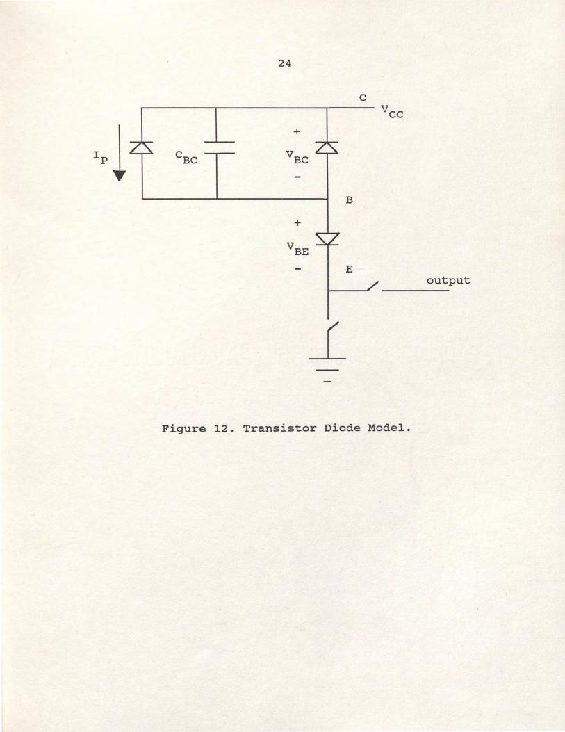
24
c
B
E output
_(
Figure 12. Transistor Diode Model.

25
Multiplexing Cells
The previous technique is an ideal approach for time
division multiplexing. Since each cell can only give an
output for part of the period and is open .for the rest of
the period, then the cells can be summed. Only one
photodetector will be sampled at a time. A block diagram is
shown in Figure 13 and a sample of the timing diagrams in
Figure 14. A detailed schematic is shown in Figure 15. The
circuit output is a time-division multiplexed waveform with
a magnitude proportional to the amount of flux incident on
the photodetector.
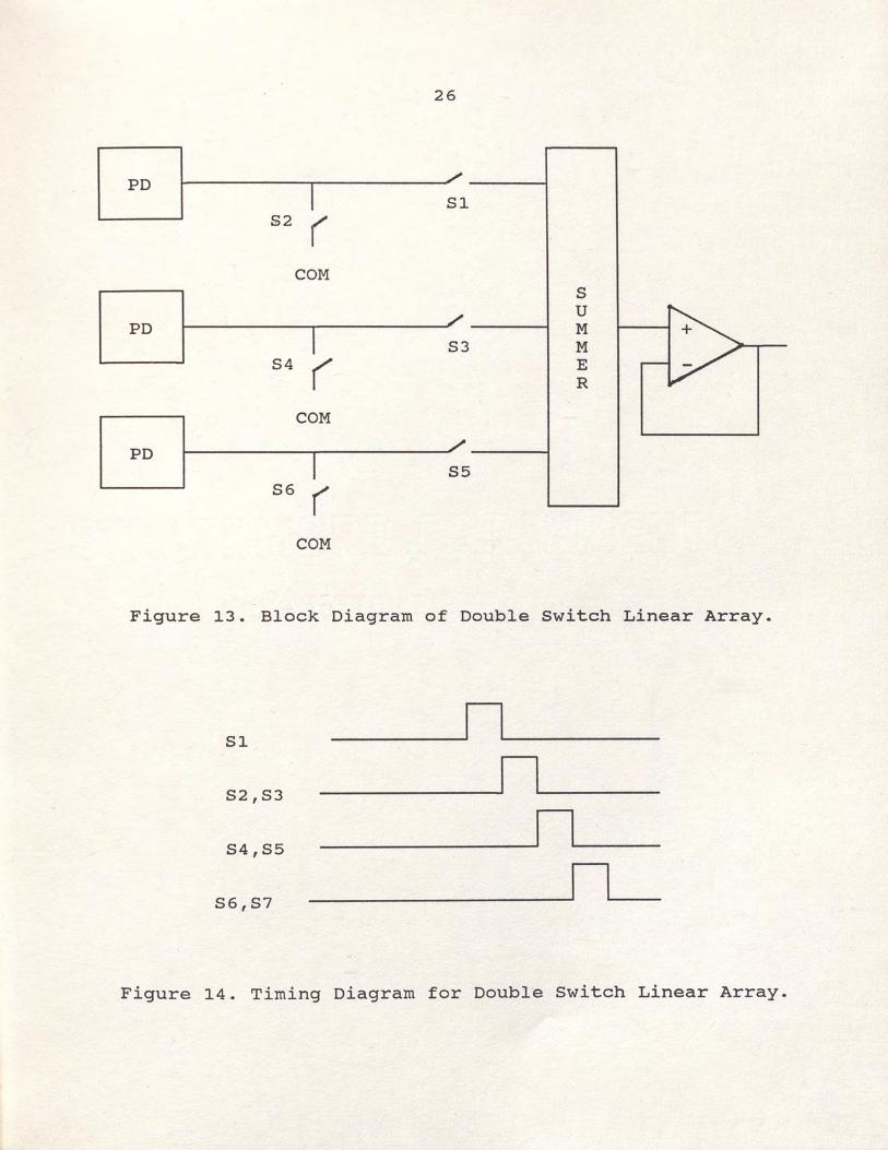
26
PD I /
Sl S2 (
COM s
/ u
PD I M S3 M
S4 ( E R
COM
PD /
I S5 S6 (
COM
Figure 13. Block Diagram of Double Switch Linear Array.
Sl
S2,S3
S4,S5
S6,S7
_ ____.n._____ __ ____,n __ ___ n..___ ---~n-
Figure 14. Timing Diagram for Double Switch Linear Array.

::ih 0sZ
( Q4 ~-"Jr
03~ Q2_ce
-= J
01~1 QO
27
OUTPUT
Figure 15. Schematic for Double Switched Linear Array.

28
This circuit was built and observed to have linear gain
as a function of clock frequency. This circuit was selected
primarily to test the concept of using transistors as a
charge storage devices. There was no noticeable crosstalk.
If there were crosstalk, it would be a · minor problem in this
design due to the large recharge time of each capacitor.
Each cell integrates for ninety percent of the time and
recharges for the other ten percent. In a subsequent design
a shorter recharge time and a longer discharge time will be
used. This can be accomplished while decreasing the amount
of FET switches used in the design. This new topology was
discovered when it was noticed the capacitance could be
recharge though the sampling switch.
There are several advantages for the linear array
approach. This circuit demonstrates relatively large signal
gain and an output which is automatically time-division
multiplexed and a linear reproduction of the input signal.
There is the ability to tell which of the pulses in the
output signal corresponds to a given detector. The amount
of gain in the circuit is easily varied by adjusting the
clock frequency. If the clock frequency were decreased the
circuit gain would increase.

29
There are several disadvantages with this approach.
There is no zero volt reference in the output. When
shipping out the information for signal processing, a
synchronous clock is needed.. Given the number of elements
in the circuit it would not be feasible to make a lengthy
array. For an array of M photodetectors an M bit Decade
counter and 2M Mosfets would be needed.
30
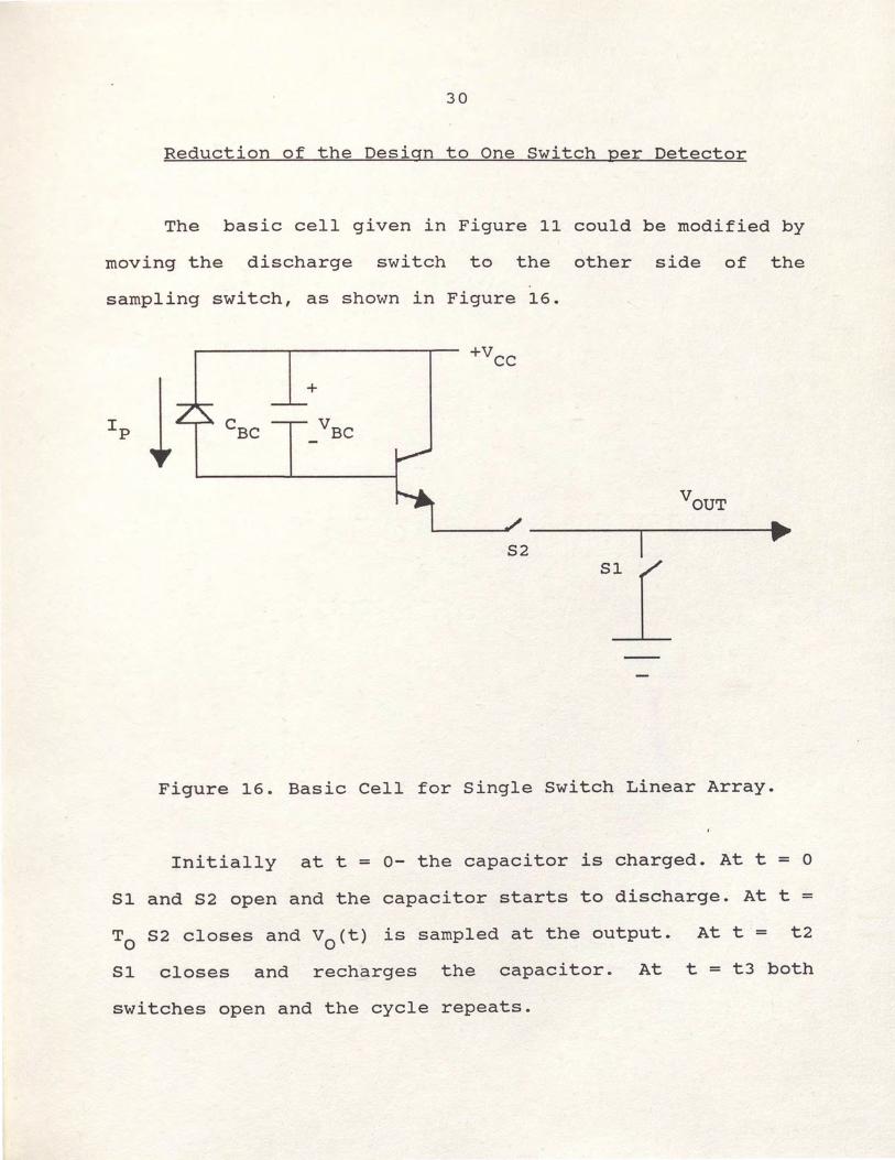
Reduction of the Design to One Switch per Detector
The basic cell given in Figure 11 could be modified by
moving the discharge switch to the other side of the
sampling switch, as shown in Figure 16.
+
S2
Figure 16. Basic Cell for Single Switch Linear Array.
Initially at t = o- the capacitor is charged. At t = O
Sl and S2 open and the capacitor starts to discharge. At t =
T0 S2 closes and v0 (t) is sampled at the output. At t = t2
Sl closes and recharges the capacitor. At t = t3 both
switches open and the cycle repeats.
31
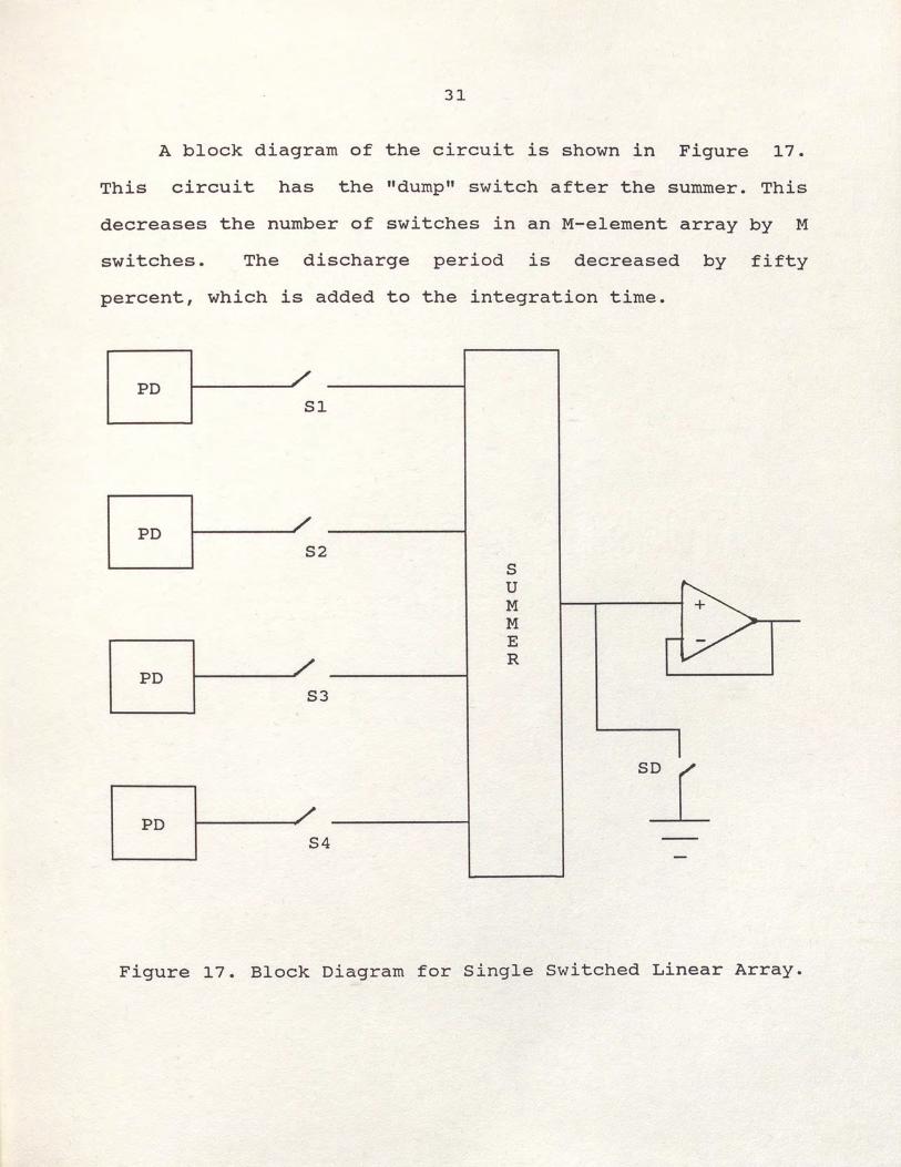
A block diagram of the circuit is shown in Figure 17.
This circuit has the "dump" switch after the summer. This
decreases the number of switches in an M-element array by M
switches. The discharge period is decreased by fifty
percent, which is added to the integration time.
PD
PD
PD
PD
1------/ Sl
/
S2
/ S3
I--___ __,/
S4
s u M M E R
s:_c_
Figure 17. Block Diagram for Single switched Linear Array.

32
00
01 VCC
02 (cc .---------i
03 T
04
OUTPUT
05
06
C---i 07
vcc
08
09 T
Figure 18. Schematic for Single Switch Linear Array.

33
Predicted Performance
When the phototransistor is used as shown in Figure 16,
the collector current is approximately zero during the
integration period and the base-emitter current is zero.
Then the base-collector voltage is equal to the emitter
voltage. Then equation (3-6) applies for the output voltage.
(3-6)
MATRIX DESIGN
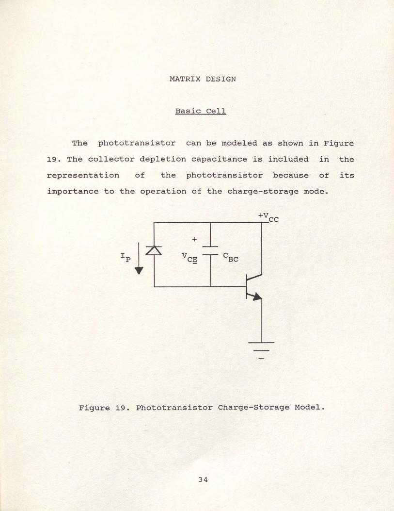
Basic Cell
The phototransistor can be modeled as shown in Figure
19. The collector depletion capacitance is included in the
representation of the phototransistor because of its
importance to the operation of the charge-storage mode.
Figure 19. Phototransistor Charge-Storage Model.
34
35
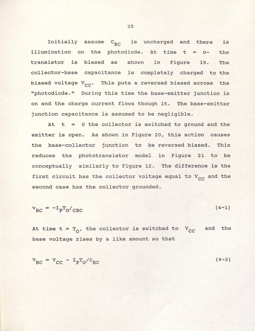
Initially assume CBC is uncharged and there is
illumination on the photodiode. At time t = o- the
transistor is biased as shown in Figure 19. The
collector-base capacitance is completely charged to the
biased voltage Vee· This puts a reversed biased across the
"photodiode." During this time the base-emitter junction is
on and the charge current flows though it. The base-emitter
junction capacitance is assumed to be negligible.
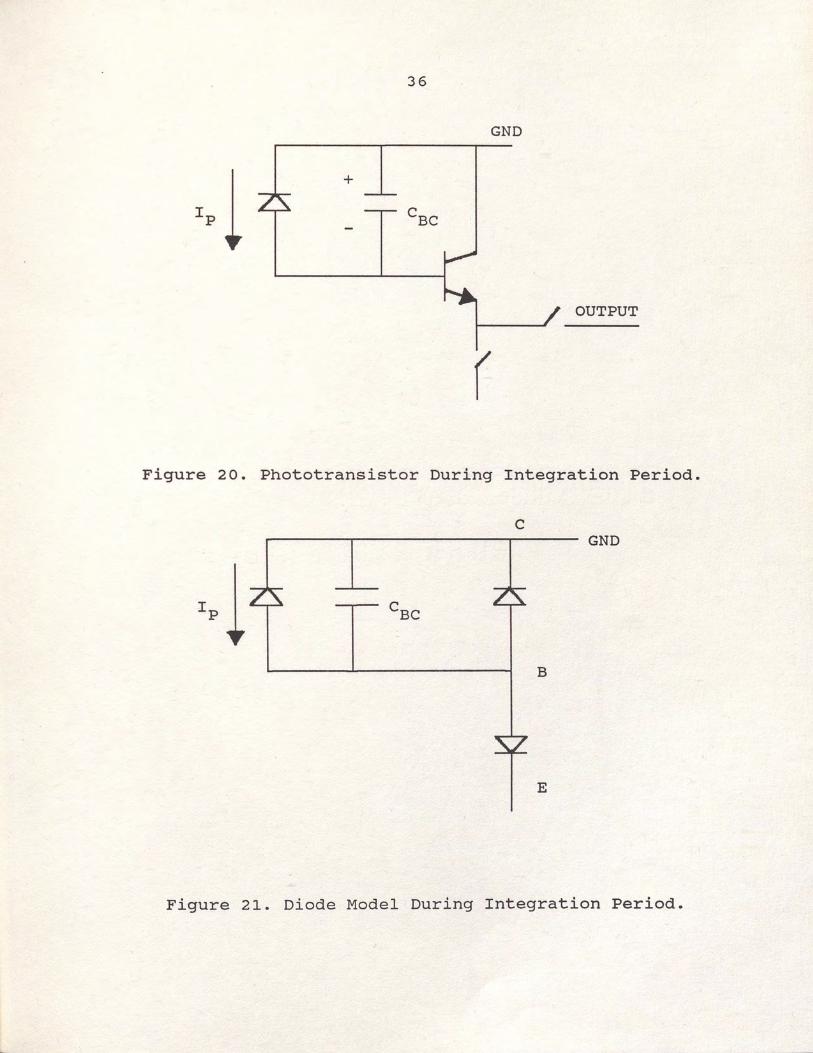
At t = O the collector is switched to ground and the
emitter is open. As shown in Figure 20, this action causes
the base-collector junction to be reversed biased. This
reduces the phototransistor model in Figure 21 to be
conceptually similarly to Figure 12. The difference is the
first circuit has the collector voltage equal to Vee and the
second case has the collector grounded.
At time t ~ T0 , the collector is switched to Vee
base voltage rises by a like amount so that
( 4-1)
and the
(4-2)
36
GND
+
OUTPUT
(
Figure 20. Phototransistor During Integration Period.
c GND
B
E
Figure 21. Diode Model During Integration Period.

37
(4-3)
At t = T0
the emitter is switched to the output and its
voltage is sampled. This voltage is buffered and the
emitter current is approximately zero, this causes the
base-emitter voltage to be zero and then the base voltage is
equal to the emitter voltage which is the output voltage.
(4-4)
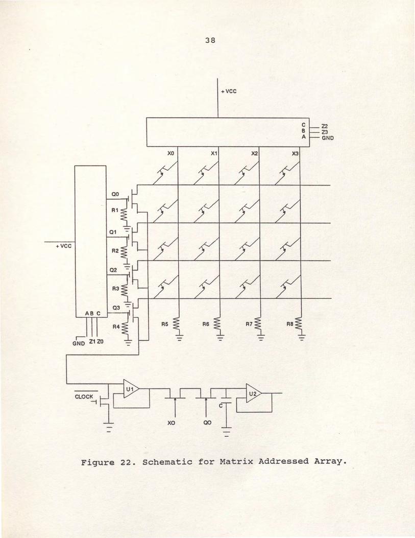
Multiplexed Array
The basic cell was put into a matrix array (Figure 22.)
and tested. This design will use CMOS technology for the
switches because CMOS provides a good bidirectional switch.
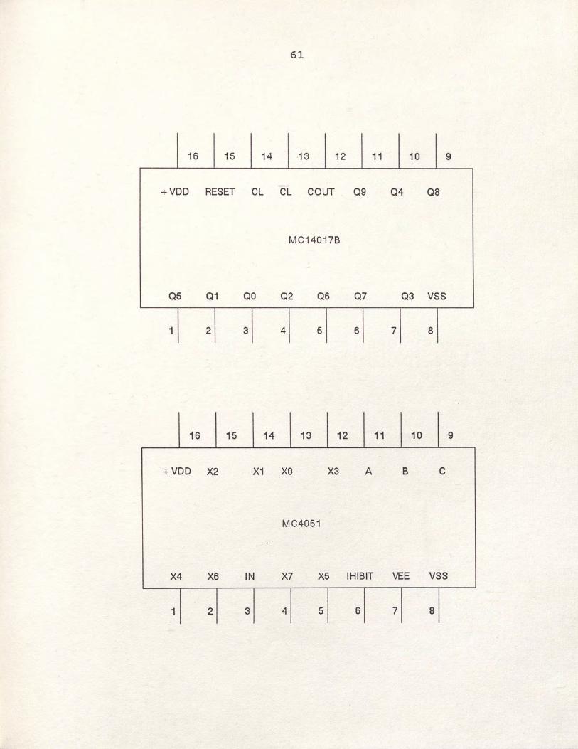
The matrix array design uses a CD4051 as the multiplexer. A
CD4066 is used to provide the switches. The opamp used is a
TL-084. Resistors Rl though R4 are used to biased the FETS.
Resistors R5 though RS are used to switch the collector
voltage from Vee to gnd. The phototransistors are from 4N25
optocouples and a signal is passed to it by the optocouple's
LED. The clocking pulses ZO, Zl, Z2 and Z3 are provided by a
four bit counter ·which is shown in appendix A. The circuit
clock is in appendix B.
+VCC
ABC
r-GNO Z1 ZO
CLOCK -1
01
R2
02
R3
03
R4
38
+VCC
c 22 B 23 A GNO
XO X1 X2 X3
--
XO
Figure 22. Schematic for Matrix Addressed Array.
DATA
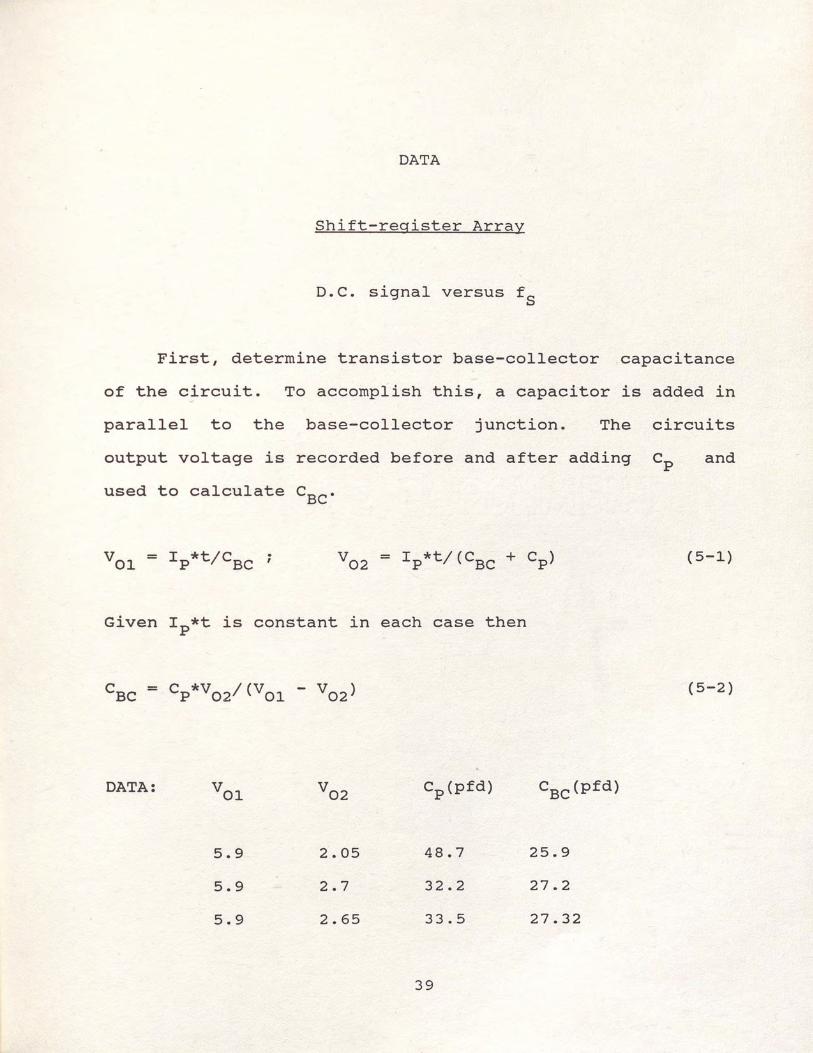
Shift-register Array
D.C. signal versus f 8
First, determine transistor base-collector capacitance
of the circuit. To accomplish this, a capacitor is added in
parallel to the base-collector junction. The circuits
output voltage is recorded before and after adding CP and
used to calculate CBc·
Given Ip*t is constant in each case then
DATA:
5.9
5.9
5.9
2.05
2.7
2.65
Cp(pfd)
48.7
32.2
33.5
39
CBC(pfd)
25.9
27.2
27.32
(5-1)
(5-2)

40
The first measurement of the design is the voltage
resulting from direct current used to power the light
emitting diode and taken as a function of clock frequency.
This is compared to a calculated value.
(5-3)
This data is tabulated in Table II, where IP is the
equivalent photo-generated current due to a given LED
current as found from Figure 4. The time "t" is integration
time. The number of photodetectors is N and N is equal to
ten.
(N - n 1 * -- (5-4)
N
This was done at two positions of the array using chip
number 29. Also in Figure 23 is a plot of vOUT versus clock
frequency for both the calculated case and the ideal case.
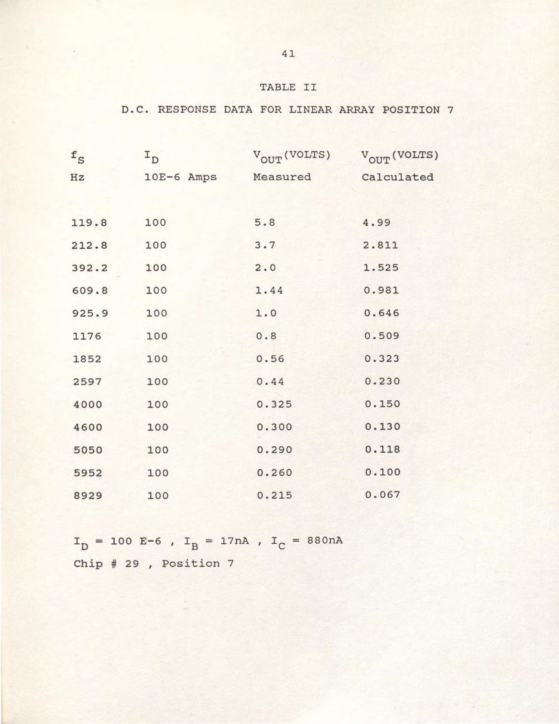
41
TABLE II
D.C. RESPONSE DATA FOR LINEAR ARRAY POSITION 7
ID
lOE-6 Amps
119.8 100
212.8 100
392.2 100
609.8 100
925.9 100
1176 100
1852 100
2597 100
4000 100
4600 100
5050 100
5952 100
8929 100
VOUT(VOLTS)
Measured
5.8
3.7
2.0
1.44
1.0
0.8
0.56
0.44
0.325
0.300
0.290
0.260
0.215
ID = 100 E-6 , IB = 17nA , IC = 880nA
Chip # 29 , Position 7
VOUT(VOLTS)
Calculated
4.99
2.811
1.525
0.981
0.646
0.509
0.323
0.230
0.150
0.130
0.118
0.100
0.067

42
TABLE III
D.C. RESPONSE DATA FOR LINEAR ARRAY POSITION 1
ID
lOE-6 Amps
116.3 100
212.8 100
392.2 100
609.8 100
925.9 100
1176 100
1852 100
2597 100
4000 100
4600 100
5050 100
5952 100
8929 100
VOUT(Volts)
Measured
5.45
3.40
1.90
1.30
0.94
0.76
0.53
0.42
0.31
0.29
0.26
0.24
0.20
ID = 100 E-6 , IB = 17nA , IC = 880nA
Chip #29 , Position 1
VOUT(Volts)
Calculated
4.98
2.811
1.525
0.981
0.646
0.509
0.323
0.230
0.150
0.130
0.118
0.100
0.067

43
-10
-20
Measured Plot -30
Calculated Plot
100 1,000 10,000
Sample frequency (hz)
Figure 23. D.C. Response Plot for Linear Array.

44
Frequency Response
The next step in testing this circuit was to measure
frequency response. The first step to accomplishing this
was to be able to observe a sinewave at the circuit output.
To do this a sample and hold circuit was developed with a
low pass filter. This enabled the signal to be recovered
from its time-division-multiplexed form. This is shown in
Figure 24. More power is needed to drive the light emitting
diode, which the circuit i .n Figure 25 does. The signal to
the LED has a D.C. bias to it. To measure the circuits
frequency response, a sinewave is applied to the circuit and
its frequency is varied. At the same time the circuits
output voltage is measured. The data is in Table V and
plotted in Figure 26.

FROM CLOCK
FROM 06
OUTPUT 4---------1
45
I 8
POLE BUlTERWORTH
LOW PASS FILTER
Figure 24. Sample and Hold Circuit for Single Switched Array

VIN
~
VBIAS
10
C1
9 R2
R1
R3
46
+7V
4
+ TL084
8
-7V
R1 = 9.86 kohm R2 = 98.7 kohm R3 = 9.94 kohm C1 = 220 nfd
R4
LED
Figure 25. Light Emitting Diode Driver Circuit.
47
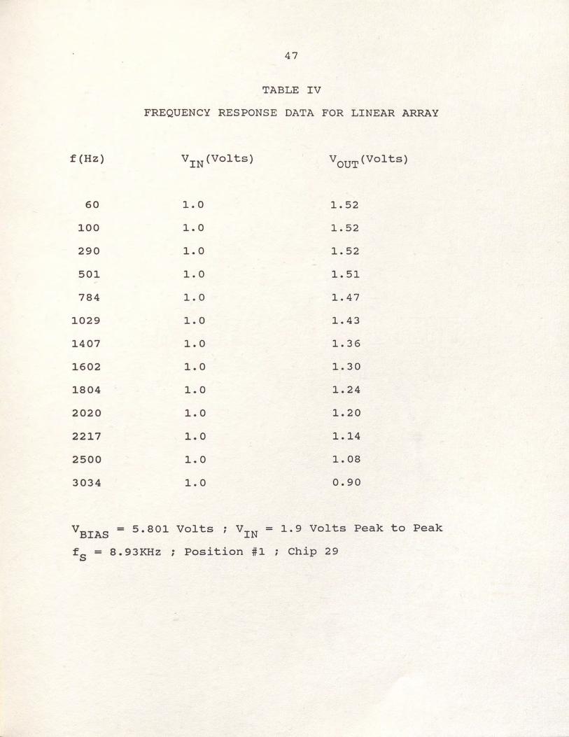
TABLE IV
FREQUENCY RESPONSE DATA FOR LINEAR ARRAY
f (Hz) VOUT(Volts)
60 1.0 1.52
100 1.0 1.52
290 1.0 1.52
501 1.0 1.51
784 1.0 1.47
1029 1.0 1.43
1407 1.0 1.36
1602 1.0 1.30
1804 1.0 1.24
2020 1.0 1.20
2217 1.0 1.14
2500 1.0 1.08
3034 1.0 0.90
VBIAS = 5.801 Volts ; VIN = 1.9 Volts Peak to Peak
f8
= 8.93KHz ; Position #1 ; Chip 29

48
VOUT(volts)
1.6
1.4
1.2
1.0
0.8
10 100 1000
Signal Frequency (hz)
Figure 26. Frequency Response Plot for Linear Array
49
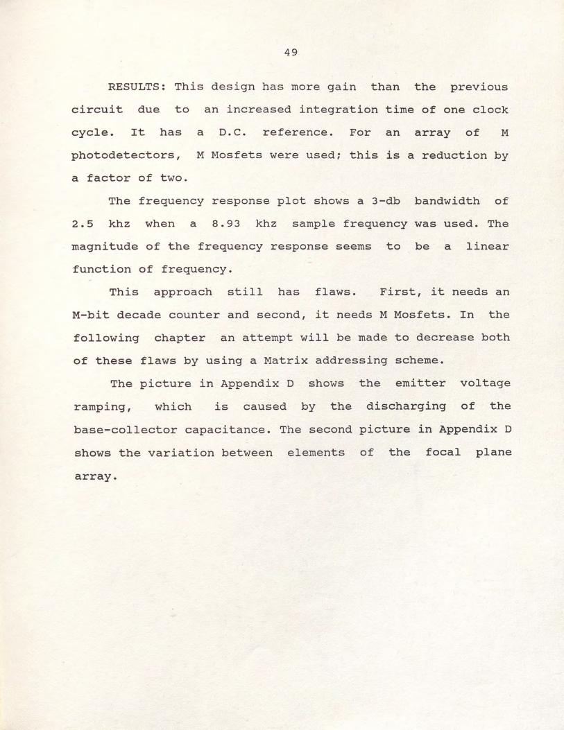
RESULTS: This design has more gain than the previous
circuit due to an increased integration time of one clock
cycle. It has a D.C. reference. For an array of M
photodetectors, M Mosfets were used; this is a reduction by
a factor of two.
The frequency response plot shows a 3-db bandwidth of
2.5 khz when a 8.93 khz sample frequency was used. The
magnitude of the frequency response seems to be a linear
function of frequency.
This approach still has flaws. First, it needs an
M-bit decade counter and second, it needs M Mosfets. In the
following chapter an attempt will be made to decrease both
of these flaws by using a Matrix addressing scheme.
The picture in Appendix D shows the emitter voltage
ramping, which is caused by the discharging of the
base-collector capacitance. The second picture in Appendix D
shows the variation between .elements of the focal plane
array.

50
Matrix Addressed Array
D.C. signal versus f 8
First, the base-collector capacitance of the transistor
in this circuit is found. To accomplish this a capacitor is
added in parallel to the base-collector junction. The
circuits output voltage is recorded before and after adding
cp_ and used this to calculate CBc·
Given Ip*t is constant in each case then
DATA:
1.28
1.28
0.67
0.745
33.5
26.0
36.8
36.2
(5-5)
(5-6)

51
The first measurement of this circuit is the voltage as
a result of direct current used to power the light emitting
diode and as a function of the clock frequency. Then this is
compared to a calculated value.
(5-7)
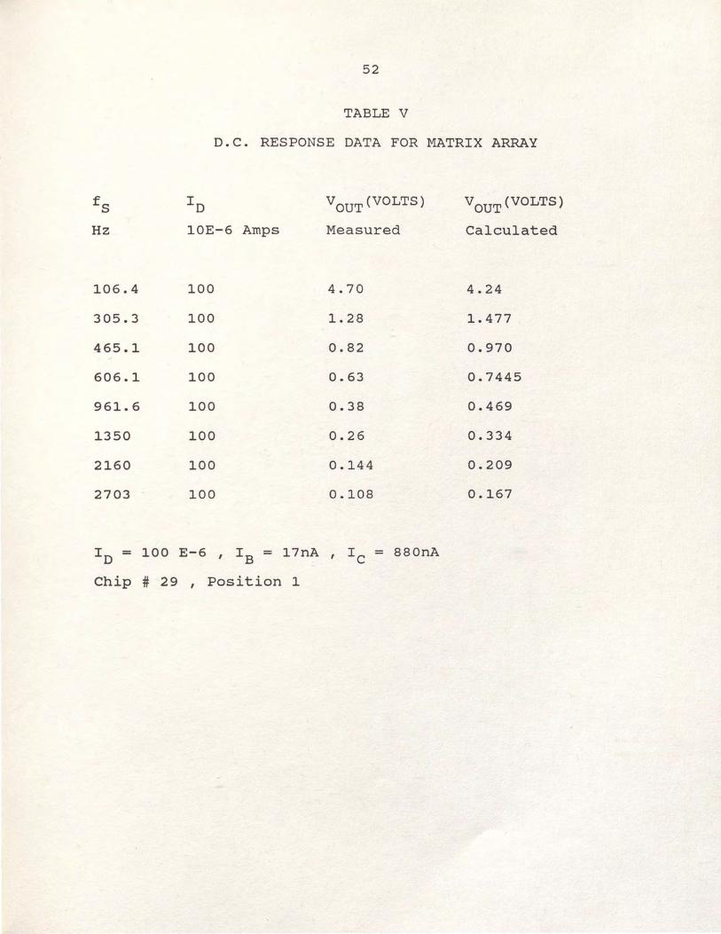
This data is tabulated in Table V, where IP is the
equivalent photo-generated current due to a given LED
current as found from Figure 4. The time "t" is the
integration time. The number of photodetectors is N and N
is equal to sixteen.
(N - 0 1 * -- (5-8)
N
This was done at position one of the array. using chip
number 29. Also, in Figure 27 is a plot of vOUT versus clock
frequency for both the calculated and ideal cases.
52
TABLE V
D.C. RESPONSE DATA FOR MATRIX ARRAY
ID
lOE-6 Amps
106.4 100
305.3 100
465.1 100
606.1 100
961.6 100
1350 100
2160 100
2703 100
ID = 100 E-6 , IB = 17nA
Chip # 29 , Position 1
VOUT(VOLTS)
Measured
4.70
1.28
Oe82
0.63
0.38
0.26
0.144
0.108
IC = 880nA
VOUT(VOLTS)
Calculated
4.24
1.477
0.970
0.7445
0.469
0.334
0.209
0.167

53
VOUT(db)
0
-10
-20
Calculated Plot
-30
Measured Plot
100 1,000 10,000
Sample frequency (hz)
Figure 27. D.C. Response Plot for Matrix Circuit.

54
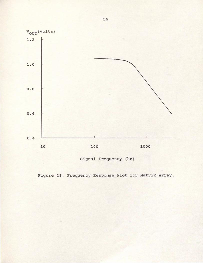
Frequency Response
The next step in testing this circuit was to measure
frequency response. The first step to accomplishing this
was to be able to observe a sinewave at the circuit output.
To do this, a sample and hold circuit with a low pass filter
was developed. This enabled the signal to be recovered from
its time-division-multiplexed form; this is shown in Figure
22. The LED was powered by the circuit used in Figure 25
with the Linear Array. The signal to the LED has a D.C.
bias to it. To measure the circuits frequency response a
sinewave was applied and its frequency varied while the
circuits output voltage was measured. The data is in Table
VI and plotted in Figure 28.

55
TABLE VI
FREQUENCY RESPONSE DATA FOR MATRIX ARRAY
f (Hz) VOUT(Volts)
97 1.0 1.04
200 1.0 1.04
411 1.0 1.02
554 1.0 1.00
803 1.0 0.92
1006 1.0 0.86
1219 1.0 0.80
1429 1.0 0.73
1644 1.0 0.68
2010 1.0 0.59
2200 1.0 0.55
2500 1.0 0.49
3021 1.0 0.40
3502 1.0 0.24
VBIAS = 5.130 Volts ; VIN= 1.9 Volts Peak to Peak
f 8 = 9.43KHz ; Position #1 ; Chip 29
56
V OUT (vol ts)
1.2
1.0
0.8
0.6
0.4
10 100 1000
Signal Frequency (hz)
Figure 28. Frequency Response Plot for Matrix Array.

57
RESULTS: This design has less gain then the previous
design due to an apparent increase of capacitance. Faster
clocks will produce less gain but are necessary to pass
signals since the Nyquist sampling rate must be met.
This frequency response plot shows a 3-db bandwidth of
1.4 khz when a 9.434 khz sample frequency is used. The
magnitude response appears to fall off linearly with
frequency.
This approach uses fewer parts than an linear array. It
has more cross coupling problems and its frequency response
is not as good. For the design of large arrays this
approach could be used to minimize the ciruit element count.
This could make this design useful if the circuit designer
is limited in the amount of parts he uses.

CONCLUSION
The traditional linear multiplexer was able to pass an
undistorted low frequency signal. The voltage gain is
inversely proportional to the sample frequency. This will
always be the case in any charge storage design. When charge
is integrated and the integration period is decreased, then
integrated charge is less. The frequency response is
constant up to 500 Hertz and then decreases six decibels per
octave. This circuit's frequency response could be
compensated. This design could be expanded by using a longer
shift register and more CMOS switches. When expanding this
design, care will have to be taken to ensure the junction
capacitance is fully recharged and cross coupling effects
are minimized.
The matrix addressed array has a frequency response
plot with the same shape as the linear array, though its
gain is decreased by a factor of four. Cross coupling is a
greater problem in this design. This design can be expanded
and will use less parts than the linear array. The amount
of MOS switches used decreases from (N+l) in the linear
array to (2*SQR(N)) with the matrix array, where N is the
number of photodetectors used in the design.
58

APPENDIX A PIN DIAGRAMS
14 13 12 11 10 9 8
+VDD
MC14011B
vss
1 2 3 4 5 6 7
59
60
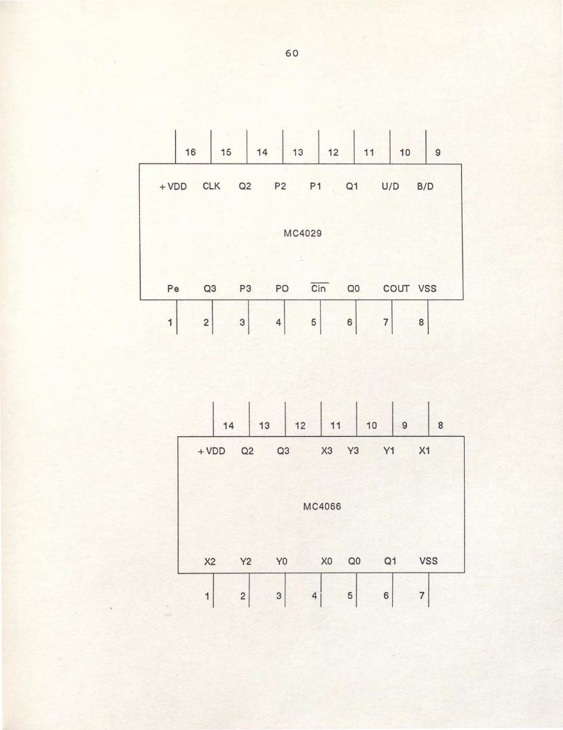
16 15 14 13 12 11 10 9
+VDD CLK 02 P2 P1 01 U/D B/D
MC4029
Pe 03 P3 PO Cin 00 COUT vss
1 2 3 4 5 6 7 8
14 13 12 11 10 9 8
+VDD 02 03 X3 Y3 Y1 X1
MC4066
X2 · Y2 YO XO 00 01 vss
1 2 3 4 5 6 7
61
16 15 14 13 12 11 10 9
-+VDD RESET CL CL COUT 09 04 as
MC14017B
05 01 QO 02 06 07 03 VSS
1 2 3 4 5 6 7 8
16 15 14 13 12 11 10 9
+VDD X2 X1 XO X3 A B c
MC4051
X4 X6 · IN X7 X5 IHIBIT VEE vss
1 2 3 4 5 6 7 8

INPUT
----1 5
+ C1 6
APPENDIX B SCHEMATICS
R1
C1 = 10.09 nfd R1 = 61.01 KOHM R2 = 10.02 KOHM
Pre - filter Amplifier
62
2
3
R2
1 OUTPUT
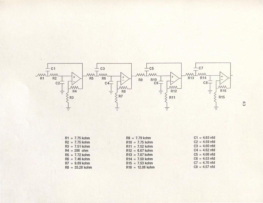
. R1 = 7.75 kohm R2 = 7.75 kohm R3 = 7.51 kohm R4 = 286 ohm R5 = 7.72 kohm R6 = 7.46 kohm R7 = 9.S9 kohm RS = 33.2S ·kohm
R9 = 7.79 kohm R10 = 7.75 kohm R11 = 7.52 kohm R12 = 6.67 kohm R13 = 7.67 kohm R14 = 7.50 kohm R15 = 7.53 kohm R16 = 12.06 kohm
C1 = 4.63 nfd C2 = 4.59 nfd C3 = 4.60 nfd C4 = 4.62 nfd C5 = 4.66 nfd C6 = 4.53 nfd C7 = 4.70 nfd CS= 4.57 nfd
°' w

CLOCK
2R R
C1
IS CnAl
50.00
5.000 /div
.0000 ___,,,,,..
• 0000
~
APPENDIX C OPTOCOUPLE PLOTS
-~ ~ -----~
~ ~ :,_,..----
IC .2000/div (UA) 2.000 .
Chip Number 1
65
IB A) Cn
50.00
5.000 /div
.000 oV /
• 0000
~v v
L
IC
66
./ v
- v-/
/~
~ ~v
'
2 . 000 .2000/div (uA)
chip Number 8

IB (nA]
50.00
5.000 /div
.000 aV • 0000
/ ,,,,,
~/
IC
67
.
~
~ ,,,_
~
~ ........
~
~/ .........
2 • 000 .2000/div (UA)
Chip Number 9

IS (nA)
50.00
5.000 /div
.000 0 ----• 0000 -----i-----
~
IC
68
~
-----~ - -----2 . 000
.2000/diV (UA)
Chip Number 12
IS (nA)
50.00
5.000 /div
oV ... . ooo .oooo
~ ,,.,,.-
~
IC
69
x
~ ~ L.:----
~ ~
------
2 . 000 .2000/div CuA)
Chip Number 18

ID (uA)
200.0
20.00 /div
.000 0 r
• 0000
~ ,,,_,,.,,--
70
- ~ :__....- -~ -
2 • 000 IC • 2000/di v CuAl
Chip Number 1

ID (uA)
200.0
20.00 /div
.ooo 0
~
I • 0000
~v ~
/
IC
71
~ ~
~
~ ~
------
2 . 000 .2000/div (UA)
Chip Number 8
ID (UA)
200.0
20.00 /div
.000 0
/ , • 0000
~ ~
~/ n
IC
72
-
~ ~ --~ ~
-----I
2 • 000 • 2000/di v CuA)
Chip Number 9
ID A) Cu
200.0
20.00 /div
.000 or • 0000
~-------'
73
-- ~ __..,,..- ,_.......
2 • 000 IC .2000/diY (UA)
Chip Number 12

ID A) Cu
200.0
20.00 /div
/ (
0 .000 .0000
/ 'tfll"
74
-~
~.--
l___....-
__..,--- --_,,,.,,--~
2. 000 IC .2000/div (uA)
Chip Number 18

APPENDIX D PICTURES
Linear Array Cell Variations
Linear Array Emitter Voltage Ramping
75

REFERENCES
(1) List, W. "Introduction to Solid-State Imaging Issue." IEEE Transactions on Electron Devices. 15 (April 1968): 190.
(2) Dyck, R. H. and Weckler, G.P. "Integrated Arrays of Silicon Photodetectors for Image Sensing." IEEE Transactions on Electron Devices. 15 (April 1968): 196-201.
(3) Biard, J. R.; Bonin, E. L.; Matzen, w. T. and Mernyman, J. D. "Optoelectronics as Applied to Function Electronic Blocks." Proceedings of the IEEE. 55 (December 1964): 1529-1536.
(4) Dereniack, Eustance. L. and Crowe, Devon. G. Optical Radiation Detectors. New York: John Wiley & Sons, 1984.
[5) Weckler,G. "Operation of P-N Junction Photodetectors in a Photon Flux Integrating Mode." IEEE Journal of Solid-State Circuits. 2 (September 1967): 65-73.
[6] Chamberlain, s. G. "Photosensitivity and Scanning of Silicon Image Detector Arrays." IEEE Journal of Solid-State circuits. 4 (December 1969): 333-42.
[7] Brugler, J. s. "Low-Light-Level Properties of the Phototransistor Charge-Storage Mode." IEEE Journal of Solid-State Circuits. 4 (June 1969): 136-144
[8] De La Moneda,F. H.; Chenette, E. R. and A.van der Zeil, "Noise in Phototransistors." IEEE Transactions on Electron Devices. 18 (June 71): 340-346.
[9] Longo, J. T.; Cheung, D. T.; Andrews, A. M.; Wang, c. and Tracy,J. M. "Infrared Focal Planes in Intrinsic Semiconductors." IEEE Transactions on Electron Devices. 25 (February 1978): 213-232.
[10] Steckl, A. J.; Nelson, R. D.; French, B. T.;Gudmundsen, R.A. and D.Schechter,"Application of Charge-Coupled Devices to Infrared Detection and Imaging," Proceedings of the IEEE. 63 (January 1975): 67-74.
76