multicrystalline and back contact buried contact silicon solar
TRANSCRIPT

Multicrystalline and Back Contact Buried Contact Silicon Solar Cells
Dissertation
zur Erlangung des akademischen Grades des Doktors der Naturwissenschaften
(Dr. rer. nat.)
an der Universität Konstanz Fachbereich Physik
vorgelegt von
Wolfgang Jooß
Tag der mündlichen Prüfung: 17. Juli 2002
Referent: Prof. Dr. Ernst Bucher Referent: Prof. Dr. Peter Wyder


Table of Contents
INTRODUCTION.............................................................................................................................................. 1
1 CONVENTIONAL BURIED CONTACT SOLAR CELLS........................................................................ 3 1.1 STATE-OF-THE-ART.................................................................................................................................... 3 1.2 PROCESS DEVELOPMENT ............................................................................................................................ 5
1.2.1 Device design..................................................................................................................................... 5 1.2.2 Processing sequence.......................................................................................................................... 6 1.2.3 Emitter diffusion ................................................................................................................................ 7 1.2.4 Low pressure CVD deposition of silicon nitride and emitter passivation.......................................... 8 1.2.5 Mechanical contact groove formation............................................................................................. 10 1.2.6 P-Al co-diffusion.............................................................................................................................. 12 1.2.7 Metallisation by electroless plating................................................................................................. 14
1.3 SOLAR CELL CHARACTERISATION ............................................................................................................ 18 1.3.1 Two-Diode model and IV-measurements......................................................................................... 18 1.3.2 Spectral response measurements and spectral analysis .................................................................. 22
1.4 SUMMARY................................................................................................................................................ 23
2 MULTICRYSTALLINE SILICON BURIED CONTACT SOLAR CELLS........................................... 25 2.1 STATE-OF-THE-ART OF BURIED CONTACT SOLAR CELLS ON MULTICRYSTALLINE SILICON................. 25 2.2 DEVICE DESIGN AND PROCESSING SEQUENCE .................................................................................... 27
2.2.1 Device design............................................................................................................................ 27 2.2.2 Processing sequence ................................................................................................................. 28
2.3 MECHANICAL V-TEXTURING............................................................................................................. 29 2.3.1 Introduction .............................................................................................................................. 29 2.3.2 The texturing process and resulting surface profiles ................................................................ 30 2.3.3 Effects of mechanical V-texturing ............................................................................................. 30 2.3.4 Alkaline and V-textured solar cells ........................................................................................... 33
2.4 GETTERING........................................................................................................................................ 34 2.4.1 The gettering process................................................................................................................ 35 2.4.2 Phosphorous gettering.............................................................................................................. 36 2.4.3 Al-gettering and P-Al co-gettering ........................................................................................... 38
2.5 MICROWAVE INDUCED REMOTE HYDROGEN PLASMA (MIRHP)- PASSIVATION............................... 41 2.5.1 Introduction .............................................................................................................................. 41 2.5.2 Hydrogen passivation of defects in silicon ............................................................................... 41 2.5.3 The MIRHP-reactor and passivation process........................................................................... 42 2.5.4 Hydrogen passivation of low lifetime multicrystalline silicon .................................................. 43 2.5.5 Determination of optimum process temperature for MIR hydrogen passivation...................... 44 2.5.6 Determination of optimum process time for MIR hydrogen passivation .................................. 46
2.6 PROCESSING OF LARGER BATCH AND MODULE FABRICATION ............................................................ 47 2.7 CHARACTERISATION OF THE BEST LARGE AREA SOLAR CELL WITHIN PROCESS I............................... 50
2.7.1 IV-measurements ...................................................................................................................... 50 2.7.2 Loss analysis ............................................................................................................................. 51
2.8 PROCESS WITH IMPROVED BULK AND REAR SURFACE PASSIVATION .................................................. 53 2.8.1 Techniques for rear surface passivation................................................................................... 53 2.8.2 Processing sequence ................................................................................................................. 55 2.8.3 Comparison of Process I and Process II .................................................................................. 57 2.8.4 Determination of optimum process temperature for MIR hydrogen passivation in Process II. 59

TABLE OF CONTENTS
2.8.5 Comparison of hydrogenation by MIR passivation and PECVD silicon nitride layers ............62 2.9 SUMMARY .........................................................................................................................................68
3 HIGHLY EFFICIENT LARGE AREA BURIED CONTACT SOLAR CELLS ON MULTICRYSTALLINE SILICON................................................................................................................69
3.1 STATE-OF-THE-ART ...........................................................................................................................69 3.2 SOLAR CELL PROCESSING...................................................................................................................70 3.3 CHARACTERISATION..........................................................................................................................72
3.3.1 Illuminated IV characteristics ...................................................................................................72 3.3.2 Dark IV and Jsc-Voc characteristics ...........................................................................................73 3.3.3 Spectral analysis .......................................................................................................................74 3.3.4 Loss analysis .............................................................................................................................76 3.3.5 Potential for further efficiency improvements in Process II......................................................77
4 BACK CONTACT SILICON SOLAR CELLS ..........................................................................................79 4.1 DEVICE DESIGNS OF BACK CONTACT SOLAR CELLS ............................................................................79
4.1.1 High efficiency devices..............................................................................................................79 4.1.2 Advantages of low cost back contact solar cells .......................................................................80 4.1.3 Device designs of low cost back contact solar cells..................................................................81
4.2 SPECIFIC PROCESS TECHNOLOGIES FOR BACK CONTACT SOLAR CELLS...............................................84 4.2.1 Electrical interconnection between front and rear contact.......................................................84 4.2.2 Definition of p and n-type contact regions on the back surface ................................................85
4.3 METALLISATION WRAP AROUND AND METALLISATION WRAP THROUGH SOLAR CELLS ..................86 4.3.1 Solar cell description ................................................................................................................86 4.3.2 Processing sequence .................................................................................................................87 4.3.3 Grid optimisation for MWA solar cells .....................................................................................93 4.3.4 Comparison of MWA/MWT solar cells with conventional BCSCs for different substrate sizes 95
4.4 EMITTER WRAP THROUGH SOLAR CELLS..........................................................................................97 4.4.1 Solar cell description ................................................................................................................97 4.4.2 Process technologies and cell layout ........................................................................................98 4.4.3 Processing sequence .................................................................................................................99 4.4.4 Optical and electrical analysis................................................................................................103 4.4.5 Enhancement in J01 due to the second carrier collecting junction ..........................................108 4.4.6 Fill factor of EWT solar cells ..................................................................................................110
4.5 INTERCONNECTION SCHEMES FOR BACK CONTACT SOLAR CELLS.....................................................111 4.6 SUMMARY .......................................................................................................................................113
SUMMARY.....................................................................................................................................................115
BIBLIOGRAPHY ..........................................................................................................................................119
AUTHOR’S PUBLICATIONS......................................................................................................................131
ZUSAMMENFASSUNG................................................................................................................................135
DANKSAGUNG .............................................................................................................................................139

Introduction About 90 % of the world’s current energy demand is supplied by fossil fuels (oil, gas,
coal) and nuclear energy. Problems associated with nuclear energy are its security, as well as disposal of nuclear by-products. Fossil fuels have only a limited availability and cause environmental problems such as the green house effect and acid rain. An important alternative source are renewable energies such as wind, water, biomass and solar radiation. In the EU White Paper for a Community Strategy and Action Plan in the Field of Renewable Energy Sources (RES), the EU targets to increase the share of RES from 6 % in 1998 to 12 % in 2010 [EU97]. Photovoltaics (PV), which is the direct conversion from sunlight into electricity, can be a major contributor to the energy mix. In this plan, the estimated contribution of PV will increase to 3 GWp by 2010.
The annual world wide production of PV modules has increased above 400 MWp with an average growth rate of about 21% in the last 14 years. Despite the remarkable growth rates, PV is currently the most expensive of the RES, but has also the largest potential. It is expected that the costs of PV systems have to be reduced by a factor of four or five in order to be competitive with conventional energy sources. The costs of PV systems in case of silicon PV can be divided into silicon wafer (30 %), solar cell processing (13 %), module fabrication (25 %) and installation/land (35 %) [Goe97]. The major contribution to the overall production is still from large companies such as Sharp and BP Solar. However, start-up companies including sunways AG, Q-Cells and Ersol in Germany set-up new production facilities in recent years. Most of the crystalline silicon solar cells are currently manufactured by thick film metallisation. Another major metallisation technique, applied for Buried Contact Solar Cells (BCSCs), is the electroless deposition of Ni/Cu/Ag. The BCSC technology was introduced at the University of New South Wales, Australia, as a low-cost route to high efficiency solar cells. Currently, BP Solar manufactures BCSCs on monocrystalline Czochralski silicon (Cz-Si) with an annual output of 11 MW in 2001. BP Solar’s cell efficiencies range between 16 and 17%, which are the highest in the industrial manufacturing of crystalline silicon solar cells.
Cheaper multicrystalline silicon (mc-Si) has replaced Cz-Si in recent years to reduce the contribution of the silicon wafer to the system costs. It is expected that mc-Si will be the dominant material for the coming years. One aim of this work is to combine the high efficiency device design of BCSCs with the economically promising material of mc-Si to fabricate highly efficient large area solar cells. Industrial manufacturing of BCSCs on mc-Si is currently not pursued mainly due to the lack of adapted processing technologies considering the intrinsic properties of mc-Si.
The BCSC technology has an additional attractive feature. It simplifies the fabrication of new solar cell designs such as back contact solar cells. Back contact cells have emitter and base contacts on the rear surface. Due to the reduction or even absence of grid shadowing losses these solar cells have a homogenous optical appearance. In densely populated areas like most parts of Europe, cost reductions are accomplished by integrating PV modules in

INTRODUCTION 2
facades and roofs replacing tiles or walls. However, the optical appearance of current PV modules prevents some from integrating PV into buildings. The investigated back contact solar cells with its high aesthetics are well suited for building integrated PV. A further cost reduction can be expected from these devices due to a simplified process for module fabrication and higher solar cell efficiencies.
Thesis outline
CHAPTER 1 introduces the device design of conventional BCSCs followed by the development of a processing sequence for BCSCs on Cz-Si. This sequence forms the basis for the process development on mc-Si as well as back contact solar cells in the following chapters. The focal point in the development is the implementation of new process technologies compared to present ones. P-Al co-diffusion for the simultaneous groove diffusion and Al alloying leads to a reduction of high temperature process steps and to an enhanced gettering action. The introduced mechanical abrasion replacing laser ablation for the formation of the contact grooves has the potential for cost reductions. The solar cell metallisation by electroless plating of Ni and Cu is described by the development of a plating sequence. The chapter finishes with a description of the applied characterisation techniques.
In CHAPTER 2, two processing sequences are investigated for mc-Si, taking into account its intrinsic properties. In Process I the rear surface is passivated by a thin evaporated Al-BSF whereas in Process II a thicker BSF layer with improved rear surface passivation is accomplished by screen printing of Al and firing. One major loss mechanism in silicon solar cell efficiency is due to the reflectivity at the front surface. Mechanical V-grooving is applied for front surface texturing and additional effects of macroscopic V-texturing are investigated. Since the lifetime of minority charge carriers is lower than in mono-Si due to a higher density of impurities and defects, two techniques are applied to increase the lifetime by bulk passivation during solar cell processing. The removal of metallic impurities from the bulk is investigated by P-, Al- and P-Al co-gettering. Hydrogen passivation of defects is included into the processing sequence by applying remote plasma hydrogenation.
The result of the second Chapter is an optimised processing sequence for mc-Si solar cells. CHAPTER 3 is devoted to the fabrication of highly efficient, large area BCSCs on mc-Si. The solar cells are characterised with respect to their major loss mechanisms and suggestions for further improvements are made.
In CHAPTER 4, industrially attractive processing sequences are developed for back contact solar cells with the Metallisation Wrap Around (MWA), Metallisation Wrap Through (MWT) and Emitter Wrap Through (EWT) design. The self-aligning nature of electroless plating metallisation facilitates the manufacturing of back contact solar cells, especially MWA and MWT cells. The back contact solar cells are characterised and simulations are carried out to quantify their efficiency potential as compared to conventional device designs.
The results of this work are industrially attractive processing sequences for multicrystalline and back contact silicon solar cells with buried contact metallisation.

3
1 Conventional Buried Contact Solar Cells
The first section of this Chapter introduces the Buried Contact Solar Cell (BCSC) concept and gives an overview of the current stage of research and manufacturing of these devices. The second section deals with the development of a processing sequence for BCSCs by the inclusion of new process technologies such as P-Al co-diffusion and contact groove formation by mechanical abrasion compared to the state-of-the-art. The process development in this Chapter is carried out on monocrystalline Czochralski silicon (Cz-Si) and forms the basis for the optimisation of a manufacturing sequence for multicrystalline silicon (mc-Si) (Chapter 2 and 3) as well as for the evolution of processing sequences for back contact BCSCs (Chapter 4). One of the key challenges in the manufacturing of BCSCs is the solar cell metallisation by electroless plating which will be optimised and characterised. The last part of this Chapter introduces the techniques applied for solar cell characterisation.
1.1 State-of-the-art
The buried contact solar cell concept was developed and patented at the University of New South Wales (UNSW) by S. Wenham and M. A. Green in the mid-eighties [Wen86], [Wen88]. The research on this type of solar cell (see Figure 1.1) was motivated by the fabrication of high efficiency solar cells applying low cost technologies. The device design includes features which are necessary to reach high conversion efficiencies: surface passivation on front and rear side, a textured front surface, a selective emitter structure and a high quality metallisation with low shadowing losses and low contact resistance.
The main advantages of BCSCs are: • Lower contact width of the finger metallisation (25-30 µm) compared to screen printed
contacts (90-150 µm) • Small finger width allows closer finger spacing, which is important for emitters with a
high sheet resistance of around 100 Ω/sqr with respect to low shading losses • High aspect ratio (ratio of finger depth to width) leading to an excellent finger
conductivity

CHAPTER 1: CONVENTIONAL BURIED CONTACT SOLAR CELLS 4
• Relatively simple and reliable realisation of a selective emitter structure even in an industrial environment with a shallow n+-diffusion on the light active front surface and a heavy n++-diffusion underneath the metal contacts
• Low contact resistance and contact recombination of the finger metallisation due to a high doping level underneath the metal contacts
• Selective metal deposition during electroless plating can be used for novel solar cell devices e.g. back contact solar cells in which interconnections between contacts on front and rear have to be metallised (see Chapter 4)
plated metalp-type
n ++n + oxide
p +
metal Figure 1.1: Device design of BCSCs as introduced at the UNSW [Gre88]. The front surface is textured with random pyramids and coated by SiO2 for the reduction of reflection losses as well as surface passivation. The front contacts are buried into the wafer leading to narrow and deep contact grooves. A selective emitter structure is realised by a shallow n+-diffusion on the light active front surface and a heavy n++-diffusion underneath the metal contacts. The solar cell is metallised by electroless deposition of Ni/Cu/Ag.
The highest efficiency reported on BCSCs under one sun illumination is 20.6% using
FZ-Si on a cell area of 12 cm2 [Gre88]. Under 20 sun concentrating light, efficiencies up to 21.5% have been obtained [Wen94]. The current research on BCSCs outside from this work is mainly focused in the inclusion of improved rear surface passivation e.g. by “floating junctions” [Wen94] as well as the development of a simplified design without selective emitter structure [Hon97]. Industrial solar cell processing
Crystalline silicon is the dominant material in the total annual shipment of solar cells world wide (340 MWp out of 401 MWp) [Pho02]. In the last years, the production of crystalline Si solar cells shifted from single crystals (139 MWp (35%) in 2001) to multicrystalline silicon (202 MWp (50%)). The majority of crystalline Si solar cells are metallised by thick film pastes. The second major technology are BCSCs. The highest average efficiencies of crystalline silicon solar cells in industrial production lines range from around 15.0% (screen printing, mc-Si) [Schmi00] up to 17% (BCSC, Cz-Si) [Bru02].
Despite the obvious advantages of BCSCs with respect to solar cell efficiency, only BP Solar currently produces BCSCs in large-scale production [Mas91], [Bru93] with an annual output of 11 MWp in 2001 [Bru02]. Several other companies showed an interest in the manufacturing of BCSCs and the technology has been transferred to Solarex [Woh91], [Nar93] (now merged with BP Solar), Telefunken [Bol89], Samsung [Cho97] and others. Up to now, none of these companies currently manufactures BCSCs in large volumes.
CHAPTER 1: CONVENTIONAL BURIED CONTACT SOLAR CELLS 5
In a study carried out by several manufacturers and institutes [Bru97] under the APAS programme of the European commission, a cost analysis was performed for different types of industrial solar cell processing sequences based on a 500 MWp scenario. The cost study included all stages of the manufacturing process: feedstock production, crystallisation, wafering, solar cell processing and module fabrication. Solar cell efficiencies of η=15% for screen printed solar cells on mc-Si and of η=18% for BCSCs on Cz-Si, on a solar cell area of 125x125 mm2 were assumed. These efficiencies have been demonstrated for screen printed solar cells [Schmi00] on production and pilot-line level. Very recently, efficiencies of 18% have been achieved by BP Solar in pilot-line production on Cz-Si [Bru02]. Within this scenario, it was demonstrated, that mc-Si solar cells with screen printed contacts can be produced with costs of 0.91 €/Wp and BCSCs on Cz-Si with 1.15 €/Wp. The higher costs per Wp for the BCSCs were caused by the significantly higher wafer costs of Cz-Si. Hence, one aim of this work was the development of a processing sequence for BCSCs on multicrystalline silicon, by combining a lower cost material with a high efficiency process in order to reach lower costs per Wp.
1.2 Process development
This section deals with the evolution of a processing sequence for conventional BCSCs on Cz-Si, which forms the basis for the development of processing sequences for mc-Si solar cells in Chapter 2 and 3, as well as for back contact solar cells in Chapter 4. In the first section, the investigated device design is introduced followed by the description of the applied processing sequence. The main part describes the applied process technologies and each individual process step.
1.2.1 Device design
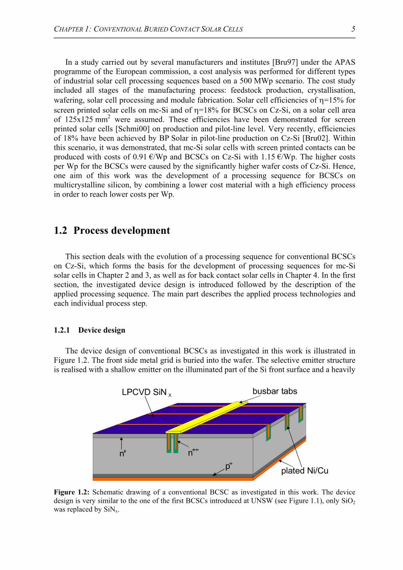
The device design of conventional BCSCs as investigated in this work is illustrated in Figure 1.2. The front side metal grid is buried into the wafer. The selective emitter structure is realised with a shallow emitter on the illuminated part of the Si front surface and a heavily
p plated Ni/Cu
LPCVD SiN
nn
busbar tabsX
Figure 1.2: Schematic drawing of a conventional BCSC as investigated in this work. The device design is very similar to the one of the first BCSCs introduced at UNSW (see Figure 1.1), only SiO2 was replaced by SiNx.

CHAPTER 1: CONVENTIONAL BURIED CONTACT SOLAR CELLS 6
diffused emitter underneath the metal contacts. The front surface is coated by Low Pressure CVD (LPCVD) SiNx which serves as Anti Reflection Coating (ARC) and for front surface passivation. The rear contact is passivated by a heavily Al-doped p+-layer (Back Surface Field (BSF)). Metallisation of the front contact fingers and the full rear side is carried out by electroless plating of Ni and Cu. The busbars consist of several contact fingers, which are tabbed by Cu ribbons during module fabrication process or in this work, for IV-measurement. This design is very similar to the first BCSCs investigated at the UNSW (see Figure 1.1), only SiO2 as dielectric on the front surface is replaced by SiNx.
1.2.2 Processing sequence
The investigated processing sequence is illustrated in Figure 1.3. The solar cell processing in this Chapter was performed on Cz-Si with a bulk resistivity of 1 Ωcm, an initial wafer thickness between 320-340 µm and a crystal orientation of <100>.
mechanical edge isolation + cleaving
metallisation by electroless Ni/Cu plating
P-Al co-diffusion950 °C, 30 min
Al evaporation2 µm
mechanical contact groove formation + defect etch
LPCVD SiN deposition
POCl emitter diffusion100 Ω /sqr
defect etch + alkaline texturing
pn+3
n+++p
x
Ni/Cu
Figure 1.3: Processing sequence for the fabrication of BCSCs during process development on Cz-Si.

CHAPTER 1: CONVENTIONAL BURIED CONTACT SOLAR CELLS 7
Processing starts with the removal of the as-cut saw damage and alkaline, anisotropic texturing (mixture of H2O, NaOH or KOH and isopropyl) leading to random pyramids. For most wafers of this work, this was done by BP Solar in their production plant in Madrid1. Phosphorous emitter diffusion is carried out at 820 °C for 20 min using a liquid POCl3 source. The sheet resistance after diffusion is in the range of 100-120 Ω/sqr which reduces to about 80-100 Ω/sqr after groove diffusion. The diffusion glass is removed in diluted hydrofluoric acid (2% HF) and SiNx is deposited in a Low Pressure CVD-reactor with a thickness of around 100 nm. Processing continues with the contact groove formation by mechanical abrasion using a dicing saw. The saw damage within the contact grooves is removed in a hot solution of NaOH. 2 µm of Al are deposited on the rear by electron beam evaporation. Then the wafers are loaded in a conventional open tube furnace for P-Al co-diffusion (950 °C, 30 min, Rsheet≈10 Ω/sqr). Metallisation is carried out by electroless plating of Ni and Cu followed by mechanical edge isolation and cleaving.
1.2.3 Emitter diffusion
Different technologies can be applied for the formation of phosphorous doped emitters in solar cell manufacturing. The most common technologies are liquid POCl3 sources, P-containing pastes deposited either by spin-on or screen printing and solid state sources. In this work only POCl3 diffusions are applied, since this technology is best suited for a homogenous diffusion within the contact grooves as well as at the edges and within the holes for back contact solar cells (see Chapter 4). For the POCl3-diffusion, the wafers are loaded in an open-tube quartz furnace. During the complete process a continuos flow of N2 is applied. Upon reaching the diffusion temperature, which is generally in the range of 800 °C to 960 °C, an additional gas flow of N2 is conducted through a container (“bubbler”) with a liquid POCl3 source. At the same time a small amount of O2 is inserted into the quartz tube. A chemical reaction occurs between POCl3 and O2 leading to P2O5 and Cl2 on the wafer surface [Goe94]. P2O5 and O2 reacts with Si on the wafer surface to form P-doped SiO2.
4 POCl3 + 3 O2 → 2 P2O5 + 6 Cl2 (1.1)
2 P2O5 + O2 + 6 Si → 6 SiO2:P (1.2)
The Phosphorous-Silicate Glass (PSG) of SiO2:P serves as P-diffusion source. Chlorine has a beneficial cleaning effect on the walls of the quartz-tube as well as on the wafer surface since it forms volatile metal compounds [Ron72]. After the diffusion, the PSG is removed during a short dip in diluted HF.
Two types of emitters are used in this work: a shallow n+-emitter at the front surface diffused at about 820 °C to 830 °C (sheet resistance Rsheet=100-120 Ω/sqr) and a deep n++-emitter within the contact grooves (950 °C, Rsheet≈10 Ω/sqr).
1 BP Solar was a project partner in the European projects ACE-Designs and ASCEMUS. Most of the work
in this thesis was conducted within these two EC-funded projects.

CHAPTER 1: CONVENTIONAL BURIED CONTACT SOLAR CELLS 8
1.2.4 Low pressure CVD deposition of silicon nitride and front surface passivation
1.2.4.1 Introduction A dielectric layer is deposited in BCSC processing after the shallow emitter diffusion.
This dielectric has to fulfil various requirements within the solar cell process and during device operation: 1. Diffusion mask for the heavy POCl3-groove diffusion 2. Mask for wet chemical process steps: saw damage removal within the contact grooves in
NaOH, P-glass removal in dilute HF acid and electroless plating of Ni and Cu 3. Antireflection coating 4. Surface passivation
Several dielectrics have been investigated in the fabrication of BCSCs. Historically, silicon dioxide SiO2 was grown in the first experiments and is still applied for the work on high efficiency BCSCs. However, due to its low index of refraction (n=1.45) the properties as ARC are not very effective when the solar cells are encapsulated. TiO2 was investigated in [Cot98] during the process development for simplified BCSCs. The main obstacle is the rather poor surface passivation properties of TiO2, when it is directly deposited onto a shallow emitter (J01e=1.4x10⁻¹² A/cm2 at Rsheet=100 Ω/sqr) [McI97]. J01e can be significantly reduced if a thin passivation oxide is grown as an intermediate layer between silicon and TiO2.
The disadvantages of SiO2 and TiO2 are not present for SiNx films which can be deposited e.g. by LPCVD or Plasma Enhanced CVD (PECVD). PECVD SiNx films have been examined at the University of Konstanz (UKN) in the processing of BCSCs by Kühn [Küh97a/b]. He observed that PECVD SiNx films do not fulfil the masking properties during the electroless plating sequence, especially at the tips of the mechanically V-textured solar cells. As described in [Küh97a/b] and in [Mas91], LPCVD SiNx fulfils all requirements for a dielectric in BCSC processing and was therefore applied in this work.
1.2.4.2 Deposition The front surface region in the investigated device design consists of a shallow emitter
which is coated by LPCVD SiNx. This “layer system” has to be optimised for the following properties (see 3. and 4. in the previous section): • Optical properties: Optimum thickness of the SiNx layer of about 75-80 nm after cell
processing leading to a low front surface reflectance and a low absorption within the SiNx layer
• Front surface passivation: High quality passivation leading to a low J01e and a high Internal Quantum Efficiency (IQE) in the short wavelength range For the deposition the wafers are placed in a quartz boat and loaded into a quartz
furnace. The wafers are heated to the deposition temperature between 750 °C and 800 °C under N2 flow. Upon reaching the peak temperature the processes gases NH3 and SiCl2H2 are introduced into the quartz tube. The gases react to SiNx according to:
3 SiCl2H2 + 4 NH3 → Si3N4 + 6 H2 + 6HCl (1.3)
The pressure is approx. 300 mTorr and the deposition rate is approx. 2.5 nm/min. The thickness of the layer has to be adjusted to obtain an optimum value in the range of 75-80 nm after solar cell processing. Several process steps in dilute HF as well as the groove

CHAPTER 1: CONVENTIONAL BURIED CONTACT SOLAR CELLS 9
diffusion affect the SiNx layer thickness with the POCl3 groove diffusion having the strongest effect. Therefore about 100 nm are initially deposited. In Figure 1.4, the optical constants n and k are shown in the wavelength range from 300-900 nm as determined by ellipsometry. k is close to zero over the complete range leading to no significant absorption within the layer.
300 400 500 600 700 800 900
2.00
2.05
2.10
2.15
2.20
k
n
n
wavelength [nm]
0.0
0.1
0.2
0.3
0.4
0.5
k
Figure 1.4: Optical constants n and k of SiNx deposited by Low Pressure CVD.
1.2.4.3 Front surface passivation
At the surface the periodicity of the lattice is disturbed leading to dangling bonds. Thereby, surface states within the band gap are created leading to Shockley-Read-Hall recombination centres. Additional treatments to passivate the surfaces are required to enhance the solar cell efficiency.
The properties of the applied front surface passivation were investigated by the fabrication of test samples (Cz-Si, specific resistivity ρ=10 Ωcm, τB=2 ms, w=380 µm). Emitter diffusion was carried out at 820 °C for 20 min (Rsheet=100-120 Ω/sqr). The phosphorous diffusion glass was removed in diluted HF prior to the deposition of LPCVD SiNx. One test wafer obtained an additional high temperature treatment at 950 °C for 30 min simulating groove diffusion. All samples were measured using Quasi Steady State PhotoConductane (QSSPC) decay [Sin96], [Fis02c]. The main parameters extracted from the measurements are the emitter sheet resistance Rsheet and the emitter saturation current density J01e
2. The results are given in Table 1-1.
Table 1-1: Emitter saturation current density J01e and emitter sheet resistance Rsheet for test samples with and without thermal treatment at 950 °C simulating groove diffusion (material: Cz-Si, 10 Ωcm).
Groove diffusion
J01e [fA/cm2]
Rsheet [Ω/sqr]
No 170 91 Yes 130 55
The quality of the emitter and front surface passivation is expressed by the saturation
current density J01e and the IQE in the short wavelength range. The obtained value of
2 The Two-Diode model as well as the characterisation of solar cells is described in section 1.3.

CHAPTER 1: CONVENTIONAL BURIED CONTACT SOLAR CELLS 10
J01e=130 fA/cm2 after groove diffusion is sufficiently low for industrial type solar cells on medium quality wafers (Cz-Si, mc-Si), since J01 will be dominated by the contribution of the base and rear J01b. The IQEs throughout this work have values close to 1 in the short wavelength range leading to low emitter losses below 0.3 mA/cm2 (see e.g. Chapter 2).
The emitter sheet resistance Rsheet after the LPCVD SiNx deposition is slightly lower for the test wafers (wafer area of 5x5 cm2) as for larger area wafers processed in the same batch (100 Ω/sqr). This can be explained by a different gas flow at the sample place. Rsheet is reduced by the subsequent groove diffusion at 950 °C to about 55 Ω/sqr. Two different effects are contributing to this reduction. First of all, the depth of the emitter is enhanced (“drive-in”) and secondly precipitated P-atoms and P-atoms in interstitial lattice sites are transformed into an electrically active substitutional lattice site [Gös91].
1.2.5 Mechanical contact groove formation
1.2.5.1 Introduction The chosen technique for contact groove formation has to lead to narrow (<25 µm) and
deep fingers (>30 µm). For industrial processing, also throughput, yield and manufacturing costs are important figures. Several techniques have been investigated in the past for groove formation. The most widely used approach is laser ablation. Lasers were used in the initial experiments at UNSW [Cho87], [Gre88] and also BP Solar applies laser ablation [Mas91]. Several attempts have been made to develop other techniques, since current laser systems mean rather high investment costs and low throughput (> 10 sec per wafer).
Another approach for contact groove formation is based on mechanical abrasion in which dicing machines are equipped with thin dicing blades. Mechanical dicing has been investigated by several research institutes and companies e.g. Solarex [Nar93], University of Konstanz [Fat94], [Küh97b] and in [Yuw97]. This work was motivated by the possible high throughput if multiple blades are used (below 10 sec [Fat98]) and also by lower processing costs. Figure 1.5 compares the shape of the contact grooves made by laser ablation and mechanical grooving [Küh97b].
Mechanical grooving is applied in this work, since contact groove formation for mechanically V-textured cells is facilitated by mechanical dicing. Due to the depth of the V-grooves of around 60-90 µm, a defocusing of the laser beam is very likely leading to inhomogenous widths and depths of the contact grooves.
Figure 1.5: Comparison of contact grooves made by (left) laser ablation and (right) mechanical dicing (from [Küh97b]).

CHAPTER 1: CONVENTIONAL BURIED CONTACT SOLAR CELLS 11
1.2.5.2 Groove geometry and alkaline saw damage removal For contact groove formation dicing blades with a thickness of 15 µm were used. The
blades consist of diamond grains with a size of 0.7-2 µm which are embedded in a nickel matrix. Mechanical abrasion by dicing blades or texturing wheels induces defects within the treated surface region. Several investigations were performed in order to determine the thickness of the damaged region [Fat98], [Ger02]. The induced saw damage can be removed by acidic or alkaline etching solutions.
The following topics are addressed in the next sections: • Groove width after plating for different etching duration • Determination of etching depth for complete saw damage removal
Experiment
In this experiment, different duration of the alkaline saw damage removal within the contact grooves were investigated. The scanning velocity during mechanical dicing was chosen to 15 mm/sec applying the single blade technique. For the experiment, solar cells were processed according to the standard sequence (see Figure 1.3) without alkaline texturing (Cz-Si, cell area 24 cm2). The saw damage within the contact grooves was removed in a hot solution of sodium hydroxide (20% NaOH) at a temperature of 80 °C. Twelve different etching duration were applied in the range of 20-360 sec. Results Contact groove geometry and etching behaviour
In Figure 1.6, top view and cross sectional pictures from contact grooves are shown after 20 sec (top, wafer 1) and 300 sec (bottom, wafer 2) of etching. The pictures of wafer 1 show, that very narrow grooves of 15 µm can be formed leading to an almost rectangular groove geometry. The top view indicates that the silicon is chipped off in some regions. The pictures of wafer 2 illustrate, that SiNx is under-etched during saw damage removal. The width of the grooves is around 28 µm, whereas the width between the remaining SiNx is still around 16 µm as it was directly after groove formation. The removal of 6.5 µm per groove side corresponds to an etching rate of 1.3 µm/min. The grooves still have a rectangular groove geometry. Therefore the etching is homogenous throughout the grooves.
The picture in the right part of Figure 1.6 shows the two wafers after electroless plating. The groove width of wafer 1 was about 16 µm after etching, after electroless plating the metallised width is about 26 µm. The enhanced width after plating is a consequence of the nature of electroless deposition and can not be avoided. The metallised groove width of wafer 2 is only 30 µm, despite a groove width of already 28 µm. The under-etched SiNx prevents the deposition of Cu in excess of the actual groove width. Removing the plated Cu after solar cell metallisation showed, that the SiNx was still present but frayed. Due to tensions during the growth of Cu, parts of the nitride were removed. Visual inspection of the other contact grooves indicated that the metallised width was in the range of 25-30 µm independent of the applied etching time.

CHAPTER 1: CONVENTIONAL BURIED CONTACT SOLAR CELLS 12
Figure 1.6: Optical microscope pictures for contact grooves after a defect etch in hot NaOH for (top) 20 seconds and (bottom) 300 seconds. The pictures on the left show the top view whereas the picture in the middle show a cross sectional view. The right pictures were taken after the electroless plating sequence.
IV-characteristics
An incompletely removed saw damage within the contact grooves has a negative influence on Voc and fill factor due to an enhanced recombination within the defected region. The IV-parameters were almost identical for etching duration between 40 sec and 360 sec, only for an etching time of 20 sec the fill factor was reduced to 75.5%. The highest fill factor of 79.8% was measured for the BCSC with an etching time of 40 sec. This high fill factor proves the high quality of the developed electroless plating sequence (see next section). Hence, an etching time of 40 sec (removes about 1 µm) was sufficient for saw damage removal. This is in accordance to investigations by Fath [Fat98]. He observed that the surface damage depends on the size of the diamonds embedded in the nickel matrix of the dicing blades and reported that for small sizes in the range of 0.5-2 µm the induced damage is about 1 µm.
1.2.6 P-Al co-diffusion
The device design of conventional BCSC needs the formation of three doping regions. The formation of highly doped regions requires high temperature furnace steps, which are a major part of the production costs [Hon94]. In this work, experiments were conducted to investigate a possible reduction of the high temperature furnace steps by combining the diffusion of two dopants in one thermal cycle: phosphorous diffusion and aluminium alloying. Besides the reduction of manufacturing costs due to the saving of additional

CHAPTER 1: CONVENTIONAL BURIED CONTACT SOLAR CELLS 13
process steps, this was also motivated by the beneficial effect of P-Al co-gettering, which is investigated in the processing of BCSCs on multicrystalline silicon in Chapter 2. P-Al co-diffusion is also very important for the manufacturing of back contact solar cells. It allows the application of a simple processing sequence for the manufacturing of Emitter Wrap Through (EWT) solar cells.
Al-alloying for Back Surface Field (BSF) formation
A thermal treatment with Al is a key process in this work due to its importance for back surface passivation by the formation of a doped p+-layer (BSF) as well as for gettering. Therefore, the complete process is described in more detail.
Si
Al
T=25°C
(a)
Si
Al-Si liquid
T>577°C
(b)
Si
Al-Si solid
T<577°C
(d)
Si
Al-Si liquid
p
T>577°C, cooling
(c)
+p+
Figure 1.7: Formation of a p+-layer by Al-alloying-
Prior to the high temperature furnace step an Al-layer is deposited on the rear surface.
Different deposition technologies exist, e.g. printing techniques (screen, roller, stencil) to deposit Al containing thick film pastes or vacuum techniques (sputtering, thermal evaporation, electron beam evaporation) to deposit high purity Al. Two methods were applied in this work: vacuum deposition by electron beam evaporation (layer thickness of around 2 µm) and screen printing of Al paste (layer thickness of around 40 µm).
For the thermal treatment, the evaporated wafers are put into an “open-tube” furnace at temperatures generally above 900 °C for duration of around 30 min at the peak temperature. When the wafer is heated above the eutectic temperature of 577 °C (Figure 1.7, b) a liquid Al-Si alloy is formed with temperature dependent composition as given by the phase diagram. On cooling, excessive Si in the liquid recrystallises and forms a layer which is heavily doped (above 1018 cm-3) with Al corresponding to the solid solubility of Al in Si at the cooling temperature. When the eutectic temperature of 577 °C is reached the remaining liquid solidifies with eutectic composition.

CHAPTER 1: CONVENTIONAL BURIED CONTACT SOLAR CELLS 14
1.2.7 Metallisation by electroless plating
1.2.7.1 Introduction An important process step is the metallisation of the front grid, since it is strongly related
to the solar cell efficiency due to shadowing and resisitive losses. Several requirements are necessary to obtain a high quality solar cell metallisation:
1. Low shadowing losses 2. Low resistive losses attained by excellent finger conductivity and low contact resistance 3. Good adhesion and long time stability 4. Low cost, high throughput and high yield
In the case of conventional BCSCs, the first and second point follow directly from the device design.
The remaining points strongly depend on the chosen metal (system) and deposition technique. One approach led to the commercial success of BCSCs and is the electroless deposition of metals from a metal salt solution (see next sections). The major advantage of this technique is its selective character, i.e. the chemical reaction of the deposition occurs only on metal and semiconductor surfaces but not on dielectrices. Hence, the front grid as well as the rear side gets metallised in the same plating sequence whereas the other regions are masked by a dielectric layer and therefore remain unplated. A different technique was investigated by Kopecek [Kop01], [Kop02]. In this approach the contact grooves are filled with Sn in a modified LPE furnace at higher temperatures. Due to capillary forces, Sn wets only the contact grooves even if no masking dielectric is present. The deposition of thick film metal pastes within the grooves by means of screen printing [Pir00], [Ara01], syringe printing and stencil printing has also been investigated. However, these techniques require alignment of the printing hardware to the contact grooves.
1.2.7.2 The metal layer system
In the industrial processing of BCSCs, a metal layer system is deposited by means of electroless plating. A thin layer of Ni is plated directly on Si, followed by a thick layer of Cu and a thin layer of Ag [Mas91]. Ni establishes the contact to the silicon whereas Cu is used for current transport. The plating of Ag is in principle not necessary but is often applied for soldering and the protection of Cu from corrosion. Cu has a low resistivity of ρCu=1.67 µΩcm and is therefore well suited for current transport. It can not be plated directly onto the silicon surface, since it has a high diffusion constant in silicon and serves as recombination centre lowering the bulk lifetime. Hence, any diffusion of Cu into the solar cell should be avoided. As an example for the high diffusion constant, Cu can diffuse 4.4 mm in silicon at a temperature of 50 °C (module temperature) in 20 years (life cycle) [Col80]. Additionally, Cu diffuses 170 µm at a temperature of 200 °C within one hour. These parameters are reached during encapsulation and lamination [Col80]. Ni as an intermediate layer between silicon and Cu prevents the diffusion of Cu into the solar cell.
1.2.7.3 Nickel as metal contact in silicon solar cells
A lot of effort was undertaken to use nickel contacts in silicon solar cells in the late seventies and early eighties [Col78], [And80], [Col80], [Tan80], [Gren81]. The aim was to achieve a good adhesion of the plated metal and a reliable Ni plating step as well as to develop a procedure for patterning of a dielectric layer on planar surfaces. In the BCSC

CHAPTER 1: CONVENTIONAL BURIED CONTACT SOLAR CELLS 15
process, the “patterning” of the dielectric is accomplished by the contact groove formation and subsequent heavy groove diffusion. The adhesion of Ni is significantly improved due to the deep contact grooves and large contact area. Therefore, most of the problems observed in the first experiments of Ni contacts are not present for BCSCs.
1.2.7.4 Electroless plating
Electroless plating of Ni was first investigated by Brenner et al. in 1946 [Bre46]. They observed that during electroplating of Ni under addition of sodium hypophosphate the plating efficiency was exceeding 100%. In general the term electroless plating is used for deposition techniques of metallic films by means of an autocatalytic chemical bath. In this heterogeneous catalytic electron transfer reaction the electrons are transferred across an interface from a reducing agent to the metal ions. This reaction occurs on metal and semiconductor surfaces but not on dielectrics. The chemical deposition of a metal from a metal salt solution is a redox reaction with both oxidation and reduction. For nickel plating with sodium hypophosphite, the chemical reaction is given by [Mal90]:
Reduction: Ni2+ + 2e- → Ni0 E0=-25 mV Oxidation: H2PO-
2- + H2O → H2PO-3 + 2 H+ + 2 e- E0=+50 mV
Redox: Ni2+ + H2PO-2 + H2O → Ni0 + H2PO-
3 + 2 H+ E0=+25 mV Besides Ni various other metals can be deposited by means of electroless plating e.g. Cu,
Cr, Co, Ag, Sn. The reader interested in more details on electrolesss plating is referred to [Mal90].
1.2.7.5 The electroless plating sequence
The electroless plating sequence investigated at the University of Konstanz and described in [Küh97a/b] was the basis for a further development. In this sequence, only the front contact was metallised by electroless plating whereas the rear contact was evaporated. With the developed sequence of this work, in addition to a homogenous deposition of the plated metals within the front grooves the plating of the rear surface was achieved.
The following plating sequence was applied:
Optional:Ni-sintering
Dip in 2% HF2-4 min
Cu-plating,40 °C, 3 h
Rinsing in de-ionised
water
Rinsing in de-ionised
water
Electroless Ni-plating,
70-75 °C, 90 s
Rinsing in hot de-ionised
water
Figure 1.8: Plating sequence for the electroless deposition of Ni and Cu.
CHAPTER 1: CONVENTIONAL BURIED CONTACT SOLAR CELLS 16
Pretreatment Before the electroless deposition of Ni, the phosphorous diffusion glass was removed in
diluted HF (2% HF, 2-3 min) followed by rinsing in de-ionised water. This step ensures that the contact grooves are free of a thick oxide layer, which would prevent the initiation of Ni-plating. The SiNx has its optimum thickness as ARC of around 75 nm after this process step.
Ni-Plating
In general, the electroless Ni plating baths consist of a source of nickel ions, a reducing agent, complexing agents and stabilisers. The most commonly applied source of nickel cations is nickel sulfate but nickel chloride and nickel acetate are also possible. As reducing agents, sodium hypophosphate NaH2PO2⋅H2O, sodium borohydride NaBH4 or dimethylamine borane (CH3)2NHBH3 can be applied. During the Ni depostion, H2 gas is released. The deposited layer is not pure Ni, but contains amounts of phosphorous, boron or nitrogen, depending on the reducing agent. Complexing agents in electroless Ni plating solutions are mostly organic acids or their salts. Their function is a buffering action preventing a decrease in the pH-value and the precipitation of Ni salts as well as reducing the concentration of free Ni ions [Mal90].
In this work, a commercially available alkaline Ni-plating solution from Shipley was used with sodium hypophosphite as complexing agent. The composition of the plating solution was used as given in the data sheet of the supplier. The pH-value was manually controlled to around pH=9 by adding NH4OH. The plating temperature was higher as suggested by the manufacturer and was in the range of 70-75 °C. The plating time was about 90 s leading to a layer thickness of around 100 nm. Very good Ni-plating was achieved with a homogenous deposition in the contact grooves and on the Al-Si alloy on the rear. The rinsing after plating was performed in hot de-ionised water in order to avoid cracking of the Ni layer due to thermal stresses as suggested in [Küh97a].
Ni-sintering (optional)
For an improved adhesion of the Ni layer, a thermal treatment can be applied with temperatures generally in the range of 200-400 °C. At these temperatures Ni and Si react to form nickel silicide. At temperatures between 250-350 °C the phase Ni2Si is formed, at temperatures between 350-750 °C NiSi and above 750 °C NiSi2 [Col78]. Ni-sintering also leads to a reduction of the contact resistance. Experiment
In the experiment, sintering temperatures of 350 °C, 370 ° and 390 °C for 10 min were applied. The Ni-sintering step was carried out in a quartz-tube under a high N2-flow during loading and unloading of the wafers in order to prevent any oxidation of the Ni [Küh97a].
The dark IV-curves as well as the fill factor of the BCSCs are shown in Figure 1.9. The highest fill factor was obtained for the BCSC without Ni-sintering and it slightly reduces for temperatures up to 370 °C. A significant reduction of the FF was determined for a Ni-sintering temperature of 390 °C. The decrease in the fill factor for all sintered cells was caused by a reduction in the shunt resistance as can be seen Figure 1.9 due to higher currents in the negative voltage range. At 390 °C an additional effect occurs leading to a deviation from the Two-Diode model. The right graph in Figure 1.9 shows the results by Cotter et al. [Cot00] obtained for Ni-sintering on simplified buried contact solar cells with

CHAPTER 1: CONVENTIONAL BURIED CONTACT SOLAR CELLS 17
varying sheet resistances between 3 and 53 Ω/sqr within the contact grooves. They state that the deviation from the Two-Diode model is caused by the formation of Schottky-contacts formed by Ni penetrating the emitter and contacting the base. In their study, this effect is most pronounced for the highest sheet resistance. The curve of the BCSC sintered at 390 °C has a similar shape as the curves in [Cot00] for higher Rsheet. Hence, the deviation from the Two-Diode model at lower voltages was most probably caused by Schottky contacts of Ni to the base, which is more pronounced at elevated sintering temperatures.
The specific contact resistivity ρc was determined by the transfer length method. ρc is 6 mΩcm2 for the unsintered solar cell and reduces to about 4 mΩcm2 for the sintered cell at 350 °C. The adhesion of the front contact as well as the obtained contact resistance was already reasonable without Ni-sintering. Therefore, the solar cells were processed without Ni-sintering throughout this work.
-0.2 -0.1 0.0 0.1 0.2 0.3 0.4 0.51E-7
1E-6
1E-5
1E-4
1E-3
0.01 no si., FF=79.2% 350°C, FF=78.9% 370°C, FF=78.3% 390°C, FF=73.3%
Cur
rent
den
sity
[A/c
m2 ]
voltage [V]
1E-8
1E-6
1E-4
1E-2
1E+0
0.0 0.1 0.2 0.3 0.4 0.5 0.6 0.7 0.8
Voltage (V)
Cur
rent
Den
sity
(A
/cm
2 )
53 Ohm/sq
45 Ohm/sq
21 Ohm/sq
11 Ohm/sq
3 Ohm/sq
Figure 1.9: (left) Dark IV-curve and fill factor for BCSC on Cz-Si for different temperatures of the Ni-sintering step under N2 for 10 min. (right) Dark IV-curves after Ni-sintering for different emitter sheet resistances within the contact grooves of simplified BCSCs [Cot00].
Cu-plating
Typical Cu plating baths contain copper salts, a reducing agent (e.g. formaldehyde), alkaline hydroxide, chelating agents (e.g. quadrol, EDTA) as well as stabilisers. The formaldehyde and hydroxide ions are the reducing force [Mal90]. The plating reaction occurring on catalytic surfaces is given by:
Cu2+ + 2 HCHO + 4OH- → Cu0 + 2 HCOO- +2 H2O + H2 (1.4)
For Cu-plating, a commercially available plating solution from Shipley was used which was operated at temperatures of around 40 °C. The plating time was 3-3 ½ h leading to a layer thickness in the range of 7-10 µm. According to the supplier, a layer thickness of 2.5 µm is deposited in the first 30 min, but the plating rate significantly reduces afterwards.
The results of Cu plating are best characterised by the optical finger width as well as by the line resistance of the finger metallisation. As already illustrated in Figure 1.6, the optical width is in the range of 25-30 µm leading to a low shadowing loss from the finger metallisation (approx. 1.9%). The line resistance as determined by four-point measurements was in the range of 500-700 mΩ/cm. With the developed plating sequence, fill factors up to 79.8% have been achieved with a series resistance below 0.4 Ωcm2 (see previous section) proving the quality of the applied metallisation.

CHAPTER 1: CONVENTIONAL BURIED CONTACT SOLAR CELLS 18
SEM picture of plated grooves are given in Figure 1.10 for mechanically V-textured solar cells (see Chapter 2). The left picture shows that a homogenous Cu deposition within the grooves can be achieved, even if the groove depth is exceeding 100 µm.
Figure 1.10: SEM pictures of plated contact grooves for mechanically V-textured solar cells.
1.3 Solar cell characterisation
1.3.1 Two-Diode model and IV-measurements
The IV-characteristic of a solar cell is generally described by the Two-Diode model [Goe94], [Gre82]3. Under illuminated conditions the IV characteristic within the Two-Diode model is given by:
sh
ss
B2
02s
B1
01ph RJRV]1))JRV(
Tknq[exp(J]1))JRV(
Tknq[exp(JJJ −
−−−+−−+−= (1.5)
q is the elementary charge, kB Boltzmann’s constant and T the temperature in Kelvin. Jph represents the photogenerated current density and Rs the series resistance. Rsh is the shunt resistance, which is a consequence of leakage current across the edges and of local disturbances of the p/n-junctions. J01 is the saturation current density of the first diode and n1 its ideality factor. J02 represents the saturation current density of the second diode and n2 its ideality factor. J02 accounts for generation/recombination currents in the space charge region (for more details see Chapter 2).
3 The reader interested in an introduction to solar cells is referred to these monographs. The following
description has only summarising character.
CHAPTER 1: CONVENTIONAL BURIED CONTACT SOLAR CELLS 19
Saturation current density J01 of the first diode The saturation current density of the first diode J01 is the sum of contributions from the
base J01b and the emitter J01e. J01b is given by:
effA
2
ieb01 LN
nqDJ = (1.6)
De is the diffusion constant of the electrons in the base and corresponds to 27 cm2/s at a base doping level of 1 Ωcm [Bas96]. ni is the intrinsic carrier density, NA the base doping level and Leff the effective bulk diffusion length. Leff is given by:
)
Lwtanh(
DLS
1)Lwtanh(
DLS
LL
Be
BB
Be
BB
Beff
+
+⋅= (1.7)
SB is the rear surface recombination velocity, LB the bulk diffusion length and w the cell thickness.
An accurate determination of J01e is difficult, since the emitter has a doping profile with no homogenous doping level. This leads to internal fields, band gap narrowing as well as spatially varying diffusion lengths and mobilities [Goe94]. However, J01e can be determined experimentally e.g. by lifetime measurements using the QSSPC-technique [Sin96] without the detailed knowledge of these parameters. The ideality factor n1 of the first diode depends on the recombination mechanisms. n1 is equal to one if the recombination mechanisms are given by Shockley-Read-Hall SRH, band-to-band Auger and surface recombination and the device is under low injection.
Series resistance Rs
The series resistance Rs is the sum of contributions from the metal contacts, the emitter, the base and the contact resistance between semiconductor and metal. The series resistance from the base as well as the contact resistance of the rear metal can be neglected for the BCSCs of this work.
The contribution of the emitter is given by:
12dRR
2
sheetemitter = (1.8)
Rsheet is the sheet resistance of the emitter and d the finger spacing. Remitter will be about 0.2 Ωcm2 for typical BCSCs of this work with Rsheet=100 Ω/sqr and a finger spacing of 1.5 mm.
The contribution of the finger metallisation for a square solar cell with one busbar is given by:
da12RR 2line
finger = (1.9)
Rline is the line resistance of the finger metallisation, a the edge length and d the finger spacing. For cells with two busbars, Rfinger is only one quarter of this value. For 5x5 cm2 and 10x10 cm2 solar cells with a line resistance of 500 mΩ/cm, Rfinger is about 0.16 Ωcm2.

CHAPTER 1: CONVENTIONAL BURIED CONTACT SOLAR CELLS 20
The contribution of the busbar for a solar cell with only one busbar (contacted at one end) is given by:
3line,B
busbar a3
RR = (1.10)
RB,line is the line resistance of the busbar. For solar cells with two busbars, contacted by two probes per busbar, Rbusbar has to be divided by four. The busbar of BCSCs consists of 15 contact fingers (RB,line=33 mΩ/cm) leading to Rbusbar of 1.3 Ωcm2. For a reduction of Rbusbar, the BCSCs are tabbed with Cu ribbons (RB,line=0.8 mΩ/cm) leading to Rbusbar of 0.03 Ωcm2. Hence for tabbed busbars, Rbusbar can be neglected.
The contact resistance Rcont of the front fingers is given by:
met
cell
ccont AA
ρR = (1.11)
ρc is the specific contact resistivity, Acell the cell area and Amet the metallised area. Two dimensional device design of buried contact solar cells
The Two-Diode model as described above is valid for one dimensional devices. Due to the deep, diffused contact grooves, BCSCs have a vertical emitter and therefore have to be considered as two dimensional devices. The effect of this 2D structure is discussed with respect to its contribution to current collection (Jsc) and to the dark saturation current densities (J01, J02). Two dimensional models of BCSC have been investigated by [Str91a], [Str91b] for thick solar cells and by [Mor95] for devices with high bulk lifetimes.
Due to the deep contact grooves, carriers can be collected in the vertical junction area leading to an increase in Jsc. This effect is demonstrated in the LBIC scans in Figure 1.11 for different wavelengths of the laser light. The current is normalised with respect to the current in the middle between two contact grooves. For the laser wavelength of 910 nm (980 nm), the normalised value was reduced by 0.3 (0.6) for improved visualisation. The LBIC scan shows that the current increases towards the contact grooves due to the vertical emitter. The increase is higher for larger wavelengths of the laser beam due to the enhanced penetration depth α-1 (α-1≈16 µm at 833 nm, α-1≈37 µm at 910 nm and α-1≈104 µm at 980 nm).
For an analysis of the increase in Jsc, the spatial distribution of Leff between the two contact grooves was determined. Whereas Leff corresponds to 177 µm in the middle between two contact grooves (assumed to be Leff on a planar cell without contact grooves), the average value was 186 µm with a peak value of 210 µm in the vicinity of the grooves. The first two values were used to calculate the difference in Jsc compared to a planar cell. The increase in Jsc is in the order of 0.1 mA/cm2 and is therefore negligible for the design (finger spacing and diffusion lengths) of this work.
The deep contact grooves enhance the contact width compared to a planar cell. The contact area increases by about 5% compared to a planar cell. J01e for a highly diffused and metallised emitter is 2x10-13 A/cm2, and 5% will not lead to a significant enhancement in J01e. The same fraction has to be added for J02 and therefore the deviations from J02 of a planar cell will be minor.

CHAPTER 1: CONVENTIONAL BURIED CONTACT SOLAR CELLS 21
0.0 0.5 1.0 1.5 2.00.0
0.2
0.4
0.6
0.8
1.0
980 nm
910 nm
833 nm
norm
alis
ed c
urre
nt [a
.u.]
position [mm] Figure 1.11: Results of spatially resolved LBIC measurements between two contact fingers for different wavelengths of the laser light. The current was normalised with respect to the current in the middle between two contact fingers.
Additional contributions to J01 due to the deep contact grooves also apply for the base contribution J01b. The additional base contribution will approach 5% from J01b of the planar cell for low diffusion lengths and vanish for larger diffusion lengths.
As a consequence, the two dimensional structure of the BCSC does not lead to significant deviations from a planar cell within the applied device design (finger spacing >> bulk diffusion length, groove depth << finger spacing).
IV-measurements and solar cell characterisation
From the illuminated IV-measurement the important parameters for solar cell operation are determined: the open circuit voltage Voc, the short circuit current density Jsc, the fill factor FF and the conversion efficiency η. All illuminated IV-measurements in this work were carried out under standard test conditions (1000 W/m2, AM 1.5, 25 °C, metal halogenide lamp as light source ). The light level was set from a calibrated reference cell and the temperature was controlled during the measurement. Besides the measurement of the dark and illuminated IV-measurement, the set-up was modified for the measurement of the Jsc-Voc characteristics, also performed at a temperature of 25 °C. In the measurement of the Jsc-Voc-curve, Voc and Jsc are determined at different illumination levels using a 500 W halogen lamp. The measured curve corresponds to the dark IV curve without series resistance Rs:
sh
oc
B2
oc02
B1
oc01ocsc R
V]1)Tkn
qV[exp(J]1)Tkn
qV[exp(J)V(J −−+−= (1.12)
The parameters of the Two-Diode model (J01, J02, Rs, Rsh) are extracted from the three IV-characteristics applying the software program IVCC [Fis00a] according to the procedure given in [Fis00b]. If not stated otherwise, the shunt resistance Rsh is determined from the dark IV curve at negative voltages, J01 and J02 from the Jsc-Voc curve with n1=1 and n2=2 and Rs from the illuminated IV-curve.

CHAPTER 1: CONVENTIONAL BURIED CONTACT SOLAR CELLS 22
1.3.2 Spectral response measurements and spectral analysis
Spectral response measurements are an effective tool for the determination of recombination parameters and loss mechanisms in solar cells since the absorption coefficient α in Si strongly depends on the wavelength. The response for short wavelengths (high α) gives information about the quality of the emitter and front surface passivation, larger wavelengths up to 1000 nm about the bulk diffusion length and rear surface recombination.
During the spectral response measurement, the solar cell is illuminated with monochromatic light of different wavelengths and the short circuit current Isc(λ) is recorded. The spectral response SR(λ) is defined by:
)(F)(I)(SR sc
λλ
λ = (1.13)
F(λ) is the power of the incident light at the wavelength λ. The External Quantum Efficiency (EQE) is obtained by replacing the currents in (1.14) with the discrete values of charge carriers and photons. The EQE determines the percentage of incoming photons at a certain wavelength contributing to the current:
λ
λλqhc)(SR)(EQE = (1.14)
h is Planck’s constant, c the speed of light and q the elementary charge. The Internal Quantum Efficiency (IQE) considers only photons which are absorbed in the cell:
)(R1
1)(EQE)(IQEλ
λλ−
= (1.15)
The principle measurement set-up is described in [Kel97] and was extended by Fischer [Fis02c]. In the first set-up the illuminated area was around 0.5 cm2. If comparative investigations for the determination of optimum process parameters were performed on neighbouring mc-Si wafers, the same crystal grain structure was illuminated to exclude any material inhomogeneities.
The new set-up allows the measurement of large area solar cells. The illuminated area is 4 cm2, and the complete cell is scanned using an xy-table [Fis02a]. Besides the SR-measurement, the hemispherical reflectivity can be recorded using an Ulbricht sphere. During the SR-measurements the solar cells were illuminated with a white bias light.
Determination of the effective diffusion length and loss mechanisms
The most commonly applied spectral analysis for the extraction of the effective bulk diffusion length Leff is performed in the wavelength range between 800-1000 nm [Bas90]. The relationship between the inverse of the IQE and the inverse of the absorption coefficient for a planar cell is given by:
effL)(
11)(IQE
1λαλ
+≈ (1.16)

CHAPTER 1: CONVENTIONAL BURIED CONTACT SOLAR CELLS 23
with Leff as given in equation 1.7. Leff can be determined by a linear fit. For a quantitative analysis several other methods have been described with different complexities. An overview is given in [Kel97]. A slightly modified procedure for the extraction of Leff was applied throughout this work [Fis02a] (see Chapter 2 for more details).
1.4 Summary
In this Chapter, a processing sequence for BCSCs was developed on Cz-Si which forms the basis for the investigations on multicrystalline (Chapter 2 and 3) as well as back contact solar cells (Chapter 4).
For front surface passivation, LPCVD SiNx was deposited on a shallow emitter with a sheet resistance of 100 Ω/sqr. The dark saturation current density of the emitter J01e is 1.3x10⁻¹³ A/cm2, which is sufficiently low that J01 is dominated by the contribution of the bulk for the solar cells investigated in this work.
Contact groove formation was carried out by mechanical abrasion leading to a groove width after dicing of about 15 µm. For the groove etch, different etching times were investigated resulting in groove widths between 16-30 µm. It was shown that a groove etch of 40 sec removing about 1 µm of silicon was sufficient for a complete removal of the saw damage. The corresponding optical width of the contact grooves after plating was between 25-30 µm independent of the applied groove damage etch.
P-Al co-diffusion as a new process step for the fabrication of BCSCs was implemented into the processing sequence resulting in a reduction of high temperature process steps and therefore of manufacturing costs.
Solar cell metallisation was investigated by electroless plating of Ni and Cu. With the developed plating sequence, the front grooves as well as the rear surface are plated simultaneously. The sequence fulfils the requirements of a high quality front surface metallisation with low shading losses (approx. 4-5%, including busbar), good finger conductivity with a line resistance of about 500 mΩ/cm and a sufficiently low contact resistance of 6 mΩcm2. For a further improvement of the metal adhesion, sintering of the Ni layer was investigated for temperatures between 350 °C and 390 °C. At higher temperatures, a deviation from the Two-Diode model was observed at low voltages leading to a reduction in fill factor. This deviation was most probably caused by Schottky contacts of Ni to the p-type base. Also the shunt resistances was reduced by Ni-sintering.
High fill factors up to 79.8% were obtained proving the quality of the developed solar cell metallisation. A higher fill factor was prevented by J02 of around 2x10⁻⁸ A/cm2 caused by junction recombination at the edges of the solar cell. The series resistance of these cells was below 0.4 Ωcm2 further proving the quality of the electroless plating sequence.

CHAPTER 1: CONVENTIONAL BURIED CONTACT SOLAR CELLS 24

2 Multicrystalline Silicon Buried Contact Solar Cells
In this Chapter the development of a processing sequence for multicrystalline silicon (mc-Si) Buried Contact Solar Cells (BCSCs) is described. In the first section, mechanical V-grooving for front surface texturing is applied and the benefits of this process step are investigated. Enhancement of the bulk diffusion length during solar cell processing is essential for reaching high efficiencies on mc-Si and is investigated by two approaches addressing different recombination mechanisms. These two mechanisms are due to metallic impurities present in the as-grown wafer and due to crystallographic defects such as dislocations and grain boundaries. Gettering of metallic impurities is examined during different treatments using P and Al. The passivation of crystal defects is investigated by hydrogen plasma treatments in a Microwave Induced Remote Hydrogen Plasma (MIRHP)-reactor. Improved rear surface passivation is achieved in the last section of this Chapter by a thicker BSF obtained by screen printing and firing of an Al thick film paste.
2.1 State-of-the-art of buried contact solar cells on multicrystalline silicon
Several investigations were carried out for BCSCs on mc-Si. The highest efficiency reported so far is η=16.7% by Zolper et al. [Zol89] at the University of New South Wales (UNSW) on a cell area of 10.5 cm2. They applied laser texturing of the front surface for the reduction of reflection losses. Solarex as industrial manufacturer also investigated BCSCs on mc-Si. Their process included mechanical V-texturing on the front surface and efficiencies of η=15.8% were reached on a solar cell area of 130 cm2. At the University of Konstanz (UKN), Kühn et al. reported an efficiency of 14.1% for mechanically V-textured solar cells on a cell area of 25 cm2 [Küh97b]. The device design in all of these investigations included a selective emitter structure. Honsberg et al. at the UNSW [Hon97] considered the development of a simplified process for mc-Si and solar grade Cz-Si in order to account for the lower bulk lifetimes of these materials. By the simplification of the processing sequence (e.g. no selective emitter structure), they expect a significant cost

CHAPTER 2: MULTICRYSTALLINE SILICON BURIED CONTACT SOLAR CELLS 26
reduction while maintaining efficiencies similar to conventional BCSCs. The objective of this work was different from their approach. Instead of an adaptation of the device design to a low quality material, the focal point was to improve the material quality by bulk passivation treatments like gettering and hydrogen passivation in order to benefit from the high efficiency device design of BCSCs. Hence, bulk passivation is a key issue throughout this work.
Manufacturing and properties of multicrystalline silicon
Multicrystalline silicon is a very attractive material for solar cell processing due to its lower wafer costs compared to monocrystalline silicon. Currently the world wide production of crystalline silicon modules has shifted from monocrystalline (139 MWp in 2001) to mc-Si (202 MW) [Pho02]. Most mc-Si wafers are produced by block casting techniques, but also ribbon silicon materials like Edge-defined Film-fed Growth (EFG) [Sto71], [Schmi00], String Ribbon (SR) [Wal98] and Ribbon Growth on Substrate (RGS) [Lan90], [Schön02b] are already manufactured or in the phase of pilot-line production.
In block casting, the liquid silicon is solidified in a crucible or mold, which consists of a high purity material like graphite, quartz, etc. Block casting processes can be distinguished from the techniques applied for melting the silicon. In directional solidification only one crucible is used for melting and crystallisation. In the casting process, the Si is liquefied in the crucible and the crystallisation is performed in the mold therefore separating the location of melting and crystallisation. Also concerning the heat extraction, one distinguishes between Bridgman/Stockbarger, Heat Exchange Method (HEM) and others. The obtained blocks have typical dimensions of around 50x50 cm2 and a block height of around 40 cm. The mc-Si wafers are cut from these blocks by wire saws with typical wafer sizes up to 15x15 cm2 and thickness in the range of 200 up to 360 µm.
All mc-Si materials have a higher defect density than their monocrystalline counterparts. The wafers have extended crystallographic defects like grain boundaries, dislocations, stacking faults and twins, which are inhomogenously distributed. Dislocations are generated during the crystal growth due to the release of plastic stress and their density can be reduced by controlled cooling. The concentration of lifetime killing metallic impurities can be high in the silicon feedstock material. The density of impurities like iron, nickel and chromium are generally in the range of 1013 to 1014 cm-3. In addition, oxygen and carbon are present with densities of several 1017 cm-3 [Mar01]. These impurities can be found in different states and are either dissolved, precipitated or are segregated at extended defects and also sometimes paired with the dopant atoms. However, the defect density depends on the growth method and detailed process of the manufacturer. The recombination strength of crystallographic defects is often high when they are decorated with oxygen atoms or metallic impurities [Law00].
Despite the high defect density in mc-Si, the initial bulk diffusion lengths LB after crystallisation are reasonable for these materials with values generally in the range between 80 to 150 µm, sometimes even higher. Also, several treatments are applied during solar cell processing to reduce the recombination activity of the defects which are referred to as bulk passivation. Metallic impurities can be removed from the active part of the solar cell by gettering (see section 4). The recombination strength of crystal defects can be reduced by the incorporation of hydrogen (see section 5). Due to variations in LB for the same material from one supplier even within one brick, comparative experiments on mc-Si require wafers which exhibit the same defect density. Due to the columnar growth of crystal grains, the

CHAPTER 2: MULTICRYSTALLINE SILICON BURIED CONTACT SOLAR CELLS 27
defect and impurity density is almost identical on neighbouring wafers cut adjacently from the same brick. Any comparative experiments for the determination of optimum process parameters were performed on neighbouring wafers.
Mc-Si from three different suppliers were used in this work: Eurosil from Eurosolare is manufactured by directional solidification [Fer98], Polix from Photowatt also by directional solidification [Ein00], and Baysix1 from Bayer is either manufactured by Bridgman or block casting [Häß00]. For Baysix and Eurosil, some properties of the materials as well as defect densities are summarised in Table 2-1. It has to be mentioned, that the properties vary strongly within the brick and ingot.
Table 2-1: Typical as-cut material properties of Baysix and Eurosil mc-Si: bulk diffusion length LB, concentration of interstitial oxygen Oi and substitutional carbon Cs as well as dislocation density ND taken from [Spi98].
Material LB [µm] Oi [cm-3] Cs [cm-3] ND [cm-2] Baysix 100-130 1-6x10¹⁷ <3x10¹⁷ 3x10⁵ Eurosil 120-150 <7x10¹⁷ 8x10¹⁶ low
2.2 Device design and processing sequence
The device design with the associated processing sequence investigated in Chapter 1 on Cz-Si was the starting point for the development of an optimised sequence for mc-Si. Additional process steps are included for front surface texturing and for bulk passivation by gettering and hydrogenation.
2.2.1 Device design
The device design is illustrated in Figure 2.1. A reduced front surface reflection is achieved by mechanical V-texturing and by the deposition of silicon nitride in a Low Pressure CVD (LPCVD)- reactor as Anti Reflection Coating (ARC). The front surface has a shallow emitter (Rsheet=100 Ω/sqr) and is passivated by LPCVD SiNx. Passivation of the rear surface is accomplished by an Al-BSF. The contact grooves are perpendicular to the V-grooves in order to minimise series resistance losses in the emitter. The cells are metallised by electroless plating of Ni and Cu.
1 The wafer plant of Bayer Solar is now operated by Deutsche Solar. The trade name Baysix was replaced
by Solsix.

CHAPTER 2: MULTICRYSTALLINE SILICON BURIED CONTACT SOLAR CELLS 28
plated Ni/Cu
silicon nitride
platedNi/Cu
p
p
nn
+
+++
Figure 2.1: Schematic drawing of a mechanically V-textured BCSC. The front surface is coated by LPCVD SiNx, which serves for surface passivation and ARC. The rear surface is passivated by an Al-BSF and the contact grooves are perpendicular to the V-grooves. The cell is metallised by electroless plated Ni and Cu.
2.2.2 Processing sequence
The applied processing sequence (Process I) is given in Figure 2.2. In the next sections, the optimum process parameters are determined for the steps given in red in Figure 2.2, namely V-texturing, gettering and hydrogen passivation. The parameters indicated for co-diffusion/gettering (section 4) and hydrogen passivation (section 5) are the optimised parameters and are applied throughout this work if not stated otherwise. The basic process steps (blue) were already discussed in Chapter 1.
Processing starts with mechanical V-texturing followed by saw damage removal in a hot solution of NaOH removing about 5-7 µm of silicon material. The wafers are loaded in an open-tube quartz furnace for the shallow emitter diffusion using a liquid POCl3-source. The temperature is in the range between 820-830 °C for diffusion times of 15-25 min. The phosphorous glass is removed in diluted HF before the deposition of SiNx with a thickness of 100 nm in an LPCVD-reactor. The thickness of the layer is reduced to its optimum value of 75 nm during subsequent process steps in diluted HF. The contact grooves are formed by mechanical abrasion using 15 µm wide dicing blades followed by the saw damage removal in NaOH. 2 µm of Al are evaporated on the rear surface and the wafers are loaded in a quartz furnace for P-Al co-diffusion/gettering. In this step, the contact grooves are heavily diffused (Rsheet≈10 Ω/sqr) and the Al-BSF is formed. Hydrogen passivation is carried out in a MIRHP-reactor at 450 °C for 120 min. Processing is completed by electroless plating of Ni and Cu followed by mechanical edge isolation and cleaving.

CHAPTER 2: MULTICRYSTALLINE SILICON BURIED CONTACT SOLAR CELLS 29
mechanical edge isolation + cleaving
electroless plating of Ni and Cu
MIR hydrogen passivation450°C, 120 min
P-Al co-diffusion/gettering950 °C, 30 min
Al evaporation2 µm
mechanical contact groove formation + defect etch
LPCVD SiN deposition100 nm
POCl emitter diffusion100 Ω/sqr
mechanical V-texturing + defect etch
3
x
Figure 2.2: Processing sequence (Process I) for mechanically V-textured BCSCs on mc-Si including bulk passivation by co-gettering and hydrogenation.
2.3 Mechanical V-texturing
2.3.1 Introduction
Front surface reflection is a considerable loss mechanism in crystalline silicon solar cells. In addition to ARCs, the surface can be textured for a further reduction of front surface reflectance. Different methods based on physical or chemical treatments can be applied [Fat98]. The most important one used in industrial production today is anisotropic alkaline texturisation in a solution of sodium/potassium hydroxide and isopropyl leading to random pyramids on <100> surfaces. Alkaline texturing is not very effective for mc-Si due to the different crystal grain orientations. Therefore effective techniques for surface texturing on mc-Si need to be independent of the crystal grain orientation. Several techniques have been investigated including chemical methods like acidic etching [Due01], isotropic dry plasma etching using reactive gases [Dek01], [Rub00] and physical methods like laser [Zol89] or mechanical texturing. For mechanical texturing different abrasive methods like wire saw grooving [Hez95], diamond scribing and high rotational dicing blades have been examined. The last mentioned method was intensively investigated at the University of Konstanz [Fat98], [Ger02], [Zec99]. Besides alkaline texturing for reference purposes, the last method with automatic dicing machines was applied in this work. In this

CHAPTER 2: MULTICRYSTALLINE SILICON BURIED CONTACT SOLAR CELLS 30
section, the texturing process is described followed by an optical analysis of the specific V-textures applied in this work. Additional effects of mechanically V-textured solar cells are discussed followed by a comparison of alkaline and V-textured BCSCs.
2.3.2 The texturing process and resulting surface profiles
Two dicing machines (DISCO DAD 341 and DAD 320) were used for the mechanical treatments of the silicon wafers. Two approaches for V-grooving were applied: single blades and texturing wheels. The surface of both texturing tools consists of a nickel matrix in which small grains of diamonds are embedded. The width of the texturing wheel is in the range of several centimetres, thus a large area wafer can be textured with a small number of cuts. The surface profile of a V-textured wafer using this approach is given in Figure 2.3 (texturing angle 80 °). Wheel texturing is a high throughput process and is therefore applicable in an industrial environment and applied at sunways AG for the manufacturing of POWER solar cells [Fat00]. A lower front surface reflection was achieved with the single blade approach. In this case the diameter of the curvature within the V-grooves can be reduced improving the quality of the V-texture. Also the angle of the V-tips was 60 ° additionally decreasing the front surface reflectance [Zec99].
Figure 2.3: Mechanically V-textured wafer applying a texturing wheel. The depth of the texture is about 80 µm.
2.3.3 Effects of mechanical V-texturing
2.3.3.1 Improvements in short circuit current density The following effects of macroscopic mechanical V-texturing can be observed leading to an increase in Jsc: 1.) Reduction of front surface reflectivity 2.) Enhancement in collection probability of minority charge carriers and higher carrier
generation in regions close to the emitter 3.) Light trapping Reduction of front surface reflectivity
For a quantification of the reduction of front surface reflectivity, test structures were processed. The front surface reflectance of the test wafers is given in Figure 2.4. Three

CHAPTER 2: MULTICRYSTALLINE SILICON BURIED CONTACT SOLAR CELLS 31
different textures on mc-Si wafers have been investigated: alkaline, V-texturing applying a structuring wheel (texturing angle 80 °) as well as single blade texturing (texturing angle 60 °). For reference, the reflection of an alkaline textured Cz-Si wafer is also depicted. Each wafer is coated with an ARC of LPCVD-SiNx (wafer thickness in the range of 320 µm, thickness of SiNx about 75 nm).
400 500 600 700 800 900 1000 11000
10
20
30
40
50
60
alkaline, mc-Si V-textured, wheel V-textured, single blade alkaline, Cz-Si
refle
ctiv
ity [%
]
λ [nm] Figure 2.4: Reflectivity of test samples from mc-Si applying three different texturing techniques. For reference, the reflectivity of an alkaline textured Cz-Si wafer is shown. All wafers are coated by LPCVD SiNx as ARC with a thickness of about 75 nm.
For a quantitative analysis of the front surface reflection, the reflectivity has to be
weighted with the solar spectrum (AM1.5). The calculations were performed under the assumption that each photon entering the wafer contributes by the generation of electron-hole pairs to the current (no recombination, IQE is equal to 1 over the complete wavelength range). For the calculations a reduced wavelength range from 300-1000 nm was taken in order to minimise the effects of rear surface reflectance. The total incident light leads to a current in this wavelength region of 35.8 mA/cm2. Mechanical V-texturing applying a texturing wheel reduces the optical loss by 1.2 mA/cm2 (see Table 2-2) compared to alkaline textured mc-Si cells. The losses are further reduced by 0.8 mA/cm2 applying single blade texturing leading to about the same losses as random pyramids on Cz-Si.
Table 2-2: Optical losses and weighted reflectance for differently textured front surfaces. The analysis was carried out in the wavelength range from 300-1000 nm. The optical generation in the bulk for a wafer with zero reflectance is 35.8 mA/cm2 in this wavelength region.
Alkaline mc-Si
V-textured Wheel, mc-Si
V-textured SB, mc-Si
Alkaline Cz-Si
Optical loss [mA/cm2] 3.21 2.03 1.26 1.13 Weighted reflectance [%] 8.97 5.68 3.51 3.16

CHAPTER 2: MULTICRYSTALLINE SILICON BURIED CONTACT SOLAR CELLS 32
Light-trapping and enhanced collection probability of minority charge carriers The positive effect of light-trapping in V-textured solar cells (single sided textured as
well as double sided textured) is important for wavelengths in the range well above 1000 nm as well as for crystalline silicon thin film solar cells and is only of minor importance in this work due to low rear surface reflectance. The reader interested in more detail on this subject is referred to the work of [Fat98], [Zec99], [Ter02].
The effect of enhanced Collection Probability (CP) was theoretically calculated and simulated by Zechner [Zec99]. The CP depends on the distance between the place of carrier generation and emitter. Due to the oblique coupling of the photons in V-textured solar cells, this distance is low for carriers generated within the V-tips. If the photons enter the solar cells in the bottom of the V-grooves, the CP is reduced compared to planar cells. This effect is illustrated by the calculation of the local IQE for V-textured cells for a wavelength of 833 nm and a bulk diffusion length of 25 µm (see left graph in Figure 2.5, [Zec99]). The IQE is lower in the bottom of the V-grooves compared to a planar one whereas it is significantly higher in the V-groove tips. As result, the IQE is elevated in the long wavelength range for V-textured cells compared to alkaline textured ones (see also Figure 2.6). Zechner performed simulations to quantify the gain in Jsc due to the enhancement in the IQE of V-textured cells as a function of the bulk diffusion length LB (see right graph in Figure 2.5). The calculations were performed for wheel textured as well as for single blade textured solar cells. The relative increase in Jsc due to this effect is highest for low bulk diffusion lengths and for single blade textured cells.
0 20 40 60 80 100 1200.55
0.60
0.65
0.70
0.75
0.80
0.85
0.90
0.95
1.00
V-tipV-bottom
V-grooves untextured
Ldiff = 25 µm
loca
l IQ
E at
λ =
833
nm
X-position of laser beam [µm]
Figure 2.5: (left) Calculated local Internal Quantum Efficiency (IQE) at a wavelength of 833 nm for a V-textured and planar cell (LB=25 µm), (right) calculated relative gain in Jsc for single blade and wheel textured solar cells due to the enhanced CP in V-textured surfaces (both from [Zec99]).
2.3.3.2 Additional effects of macroscopic V-texturing
The macroscopic V-texture leads to an enlarged surface area depending on the texturing angle. This is often described by the geometry factor G. G is defined by the surface area of a textured solar cell divided by the surface area of an untextured cell with the same edge length. The relationship between G and the texturing angle α at the tips of the V-grooves would be )2/sin(/1G α= with no curvature in the bottom of the grooves. The surface enlargement affects the dark saturation current densities of the first (J01) and second diode (J02) and therefore influences Voc and FF. The contribution to the emitter (J01e) increases by

CHAPTER 2: MULTICRYSTALLINE SILICON BURIED CONTACT SOLAR CELLS 33
the factor G. The increase in J01 due to a higher J01e will be low for device designs with a high quality emitter and front surface passivation like BCSCs as well as for cells which are dominated by J01b. The additional contribution of the base J01b will depend on the diffusion length LB. For very low LB below 10 µm, J01b will also increase by the factor G whereas for high LB and excellent rear surface recombination, J01b will remain unchanged. Due to the removal of silicon material by texturing, J01b can be reduced depending on LB and rear surface passivation [Fat98]. For cells investigated in this work LB is in the range between 150 µm to 400 µm. In this case, a simple expression for J01 as function of G can not be derived. According to numerical simulations in [Zec99], the decrease in Voc due to enhanced J01b for the diffusion lengths of this work will be below 2 mV.
The contribution to J02 from the unmetallised part due to the surface enlargement is more severe for the conversion efficiency, especially if J02,pl for a planar cell is already in the range of several 10-8 A/cm2 as it is the case for some mc-Si BCSCs in this work. Assuming a geometry factor of G=2 and J02,pl of 5x10⁻⁸ A/cm2, V-texturing leads to a decrease in FF of ∆FF=2.0%abs. and Voc of ∆Voc=5.7 mV.
The effects discussed up to now are independent of the solar cell design and metallisation technique. Beneficial effects occur for BCSCs, when the contact grooves are perpendicular to the V-grooves and the depth of the contact grooves is the same as for planar cells, but measured from the bottom of the V-grooves. In this case, macroscopic V-texturing reduces the series resistance. The series resistance in the emitter Remitter is reduced by the factor G. Due to a higher surface area within the contact grooves (e.g. it will be doubled for a texturing angle of 60 ° and a height of the V-grooves of 80 µm) the finger conductivity is enhanced and the contact resistance is reduced. Since Rcontact is already low for BCSCs, the effect on Rs will be minor. But the series resistance of the finger metallisation Rfinger will be lower. Therefore the two largest contributions to Rs, Rfinger and Remitter, will be reduced for mechanically V-textured solar cells depending on the geometry factor G.
2.3.4 Alkaline and V-textured solar cells
For an analysis of the effects of V-texturing discussed in the previous section, solar cells were processed according to the sequence given in Figure 2.2 and compared to alkaline textured ones. V-texturing was performed by a texturing wheel with an angle of 80 ° leading to a surface enlargement of approx. G=1.5. The experiment was performed on Baysix mc-Si (ρ=1 Ωcm, thickness 330 µm).
The illuminated IV-parameters as well as the parameters of the Two-Diode model are given in Table 2-3.
Table 2-3: Results of illuminated IV-measurements and parameters of the Two-Diode model of an alkaline textured and a mechanically V-textured BCSC on Baysix mc-Si (cell area 24 cm2).
Text. Voc [mV]
Jsc [mA/cm2]
FF [%]
η [%]
J01 [pA/cm2]
J02 [nA/cm2]
Rsh [Ωcm2]
Rs [Ωcm2]
Alk. 611 32.5 76.3 15.2 1.1 50 4000 0.7 V-text. 608 34.0 76.7 15.9 1.1 81 20000 0.43

CHAPTER 2: MULTICRYSTALLINE SILICON BURIED CONTACT SOLAR CELLS 34
Discussion V-texturing led to an increase in Jsc of 1.5 mA/cm2. The gain due to the reduction in
front surface reflectance depends on the IQE. The calculations illustrated in Table 2-2 are performed for an IQE of one. Considering the measured IQE of the planar cell and the two reflectivity curves, the increase due to the reduction of front surface reflection amounts to 1.1 mA/cm2. An additional gain is due to the enhanced IQE in the long wavelength range. This effect is illustrated for the two cells in Figure 2.6. From a spectral analysis of the planar cell, LB was determined to be 185 µm. According to the simulations performed in [Zec99] (see Figure 2.5) the relative increase in Jsc due to the improved IQE in the long wavelength range for LB of 185 µm will be 1.2% corresponding to 0.4 mA/cm2.
600 700 800 900 1000 1100 12000
20
40
60
80
100
IQE, wheel IQE, alkaline refl, wheel refl, alkalineIQ
E, re
fl [%
]
λ [nm] Figure 2.6: Internal Quantum Efficiency (IQE) and reflectivity of alkaline textured and mechanically V-textured BCSCs.
J01 is identical for both solar cells, indicating that for the applied texture and Leff, the
increase in J01e and the reduction of J01b due to the removal of bulk material are balanced. However, J02 was increased by about the geometry factor G as it is expected according to the discussion of the previous section. The higher J02 reduces Voc and FF. Since also the series resistance is lower for the V-textured cell, a higher FF was measured for the V-textured cell.
2.4 Gettering
High temperature processing influences the bulk diffusion length, since impurities are highly mobile at elevated temperatures and precipitates can be dissolved releasing metallic impurities. In the first part of this section, the gettering process as well as gettering models are described. In the following, different gettering treatments like P-, Al- and P-Al co-gettering are applied to mc-Si BCSCs. The motivation for the investigations is the optimisation of the high temperature furnace steps with respect to their gettering efficiency.

CHAPTER 2: MULTICRYSTALLINE SILICON BURIED CONTACT SOLAR CELLS 35
2.4.1 The gettering process
Metallic impurities like Fe, Co and Ni lead to deep recombination centres near the centre of the band gap. These defect states reduce the lifetime of minority charge carriers by Shockley-Read-Hall (SRH) recombination. The purpose of gettering is to remove the lifetime reducing impurities from the active part of the device. During the gettering step the impurities are captured in regions where they are less harmful for the device or where they can be removed in a subsequent etching step. Gettering is generally carried out at temperatures between 600 °C and 1000 °C.
Concerning the location of the gettering region one distinguishes between intrinsic and extrinsic gettering. In intrinsic gettering, the gettering region is within the bulk of the silicon wafer. This technique is applied in IC-technology since the active region is near the surface. Here, oxygen precipitates grown in the bulk serve as gettering region [Schrö91]. In extrinsic gettering the gettering region is close to the surface.
The gettering process can be divided in three basic steps (see Figure 2.7) [Kan89]: (1) Release of impurities (2) Fast diffusion (3) Capture in gettering region
(1) release (2) diffusion (3) captureE
active region gettering region Figure 2.7: The three basic steps in the gettering process: Release of the impurity in the active device region (1), diffusion to the gettering region (2), in which the impurity is captured (3). The gettering techniques differ in the region and form of the gettering place (from [Kan89]).
Concerning the gettering models, one distinguishes between three different mechanisms
[Schrö91]: • Relaxation-induced gettering • Segregation-induced gettering • Injection-induced gettering
In relaxation-induced gettering, a supersaturation of metallic impurities as well as a higher density of nucleation seeds for metal precipitates is required in the gettering region. As long as the temperature remains constant, gettering will not occur if the density of the impurities is below the solubility limit. A supersaturation is reached by cooling of the sample. Due to the higher density of nucleation sites in the gettering region the growth of

CHAPTER 2: MULTICRYSTALLINE SILICON BURIED CONTACT SOLAR CELLS 36
metal precipitates occurs at a lower density of the impurities. This process is called relaxation-induced gettering since the supersaturated “solution” can relax due to the nucleation sites.
In the other two mechanisms the impurities diffuse into the gettering regions already during the high temperature treatment. In segregation-induced gettering, the impurities have a higher solubility in the gettering region or new metallic compounds are formed.
Injection-induced gettering requires interstitial Si (Sii). In this gettering mechanism Sii transforms the metallic impurity by a kick-out mechanism from a substitutional lattice site Ms into an interstitial lattice site Mi.
Ms + Sii → Mi “Kick-out” By this mechanism the impurities are transformed from a state of high solubility and low
diffusion constant in a state of low solubility and high diffusion constant. Additionally Sii supports the dissolution of metal precipitates [Gös91].
Since the active region of a solar cell extends over the complete wafer volume extrinsic gettering is applied in solar cell processing. The gettering region should be located near the surface where the impurities can be removed in a subsequent etching step or are located in a layer which already has a high density of “defects” (doping regions like emitter and BSF). In these heavily doped regions with already low lifetimes due to Auger recombination, the presence of SRH-recombination centres is less harmful for the lifetime. Different techniques for external gettering have been investigated including deposition of a metal layer (Al) [Apel94], [Jos95], [Mar95], diffusion (P) [Our84], [Cue97], mechanical damage of the surface [Pom67] and ion implantation [Nas82].
This work deals with the application of gettering techniques for industrial solar cell processes. Techniques are best suited which are already an integral part of the processing sequence. Treatments wtih P and Al are applied for the formation of emitter and BSF and are therefore examined in this work.
2.4.2 Phosphorous gettering
High P-gettering temperatures were selected to examine the response of three mc-Si materials to high temperature processing since [Mah97] reports that LB of some mc-Si is deteriorated during high process temperatures. The experiment gives an indication whether the mc-Si material is suited for the manufacturing of BCSC, which generally requires high processing temperatures during groove diffusion. If a positive P-gettering effect is observed, this process step could in principle be applied prior to solar cell processing (“pregettering”).
Experiment
Phosphorous gettering was investigated by P-diffusions using a liquid POCl3 source (see Chapter 1 for the process description). The response to gettering treatments is quantified by the determination of the bulk lifetime τB or bulk diffusion length LB. Therefore, this experiment was not carried out on solar cells, but test wafers were fabricated. Figure 2.8 describes the process steps applied in this experiment.

CHAPTER 2: MULTICRYSTALLINE SILICON BURIED CONTACT SOLAR CELLS 37
P-gettering960°C, 40 min
alkaline defect etch
lifetime measurements using QSSPC
LPCVD-SiN, both sides
POCl emitter diffusion, 820°C, both sides
alkaline defect etch
P-gettering930°C, 60 min
3
1 2
3
Figure 2.8: Process flow for the investigations on P-gettering.
For the experiment four different mc-Si materials were selected with a wafer size of
12.5x12.5 cm2: Eurosil from two different deliveries (specific resistivity ρ=1.8 Ωcm, wafer thickness w=350 µm), Baysix (ρ=0.8-1.2 Ωcm, w=330 µm) and Polix (ρ=0.5 Ωcm, w=380 µm). Processing of the test wafers started with the removal of the saw damage by an alkaline defect etch followed by dips in diluted HCl and HF for wafer cleaning. The selection of the temperatures were done with respect to the peak temperature reached during BCSC processing (950 °C). Two P-gettering temperatures of 930 °C and 960 °C were chosen. The diffusion time at the peak temperature was 40 min at 960 °C and 60 min at 940 °C, therefore the total process time remained the same. After P-gettering the diffusion glass was removed in diluted HF and the highly diffused and damaged region was removed in NaOH with a thickness exceeding 8 µm as suggested in [Nag97]. For lifetime measurements, the surfaces have to be passivated. Therefore the wafers obtained a shallow POCl3-emitter diffusion at 820 °C and LPCVD-SiNx was deposited. The gettering effect of this P-diffusion can be neglected [Mac01]. The process parameters for these two steps were the same as in the processing of BCSCs. This leads to J01e=1.7x10⁻¹² A/cm2, which can also be expressed as effective surface recombination velocity Seff. Seff depends on the base doping level and is given by Seff=220/ρ cm/s, where ρ is the specific resisitivity given in Ωcm. The relationship between the measured effective lifetime τeff and the bulk lifetime τB is:
wS211 eff
Beff
+=ττ
(2.1)
w is the wafer thickness. The last term in equation 2.1 is only valid for small and constant Seff. From the measured τeff, τB was calculated according to equation 2.1. In order to investigate the effectiveness of P-gettering, wafers without this process step were processed in parallel. The defect etch was adjusted, so all wafers had the same thickness. Results and discussion
The effective lifetime was determined by Quasi-Steady State PhotoConductance (QSSPC)-decay measurements [Sin96], [Fis02c]. The QSSPC measurements were carried

CHAPTER 2: MULTICRYSTALLINE SILICON BURIED CONTACT SOLAR CELLS 38
out at eight positions on the wafer. The illuminated area corresponds to about 4 cm2, and the lifetime was extracted at an excess carrier density of ∆n=1x1016 cm-3 to exclude any trapping effects [Mac01]. The average bulk lifetime τB,ave is given in Table 2-4. The measurement at neighbouring wafers was performed at the same position with identical crystal grain structure.
Table 2-4: Average bulk lifetime τB,ave in µs determined from QSSPC-measurements.
Material Ungettered P-gettering, 960°C P-gettering, 930°C Eurosil I 8.3 16.0 14.8 Eurosil II 14.0 21.6 19.2
Baysix 20.8 17.7 18.4 Polix 10.4 8.5 8.2
τB,ave of the ungettered Eurosil I was 8.3 µs and it was almost doubled to 16 µs for the
P-gettering temperature of 960 °C. The higher gettering temperature was superior to the one at 930 °C. The same effect can be observed for Eurosil II with an increase from 14 µs to 21.6 µs. A positive effect of P-gettering on Eurosil was also found in other investigations [Cue97]. McDonald [Mac01] observed on Eurosil, that the increase in τB due to P-gettering depends on the brick position. P-gettering was most effective for wafers from the top region of the ingot whereas the effect was reduced for wafers from the middle and almost no response can be found for wafers from the bottom. The Eurosil wafers for this experiment were from the middle region of the ingot.
τB,ave of the ungettered Baysix wafer was already relatively high and was slightly reduced due to P-gettering at the investigated process temperatures. The reduction in τB,ave was elevated for the higher gettering temperature of 960 °C, suggesting that Baysix material degrades during high temperature processing. The result is in contradiction to Nagel et al. [Nag97] who observed an increase in τB due to P-gettering on Baysix for temperatures up to 1000 °C.
The results on Polix are similar to the ones for Baysix with a slight degradation of τB,ave during high temperature processing.
In summary, it can be concluded, that Eurosil benefits from P-gettering. For Baysix and Polix, the high process temperatures applied for P-gettering led to a reduction in τB,ave. However, the deterioration is moderate and both materials can be subjected to high temperature processing required for the fabrication of BCSCs without a significant decrease in cell performance.
2.4.3 Al-gettering and P-Al co-gettering
The processing of BCSCs requires several high temperature furnace steps for the formation of highly doped regions, which have a certain degree of freedom concerning process temperatures and times. Hence, the most obvious approach for bulk passivation is to optimise these steps for effective gettering action. This section deals with the determination of an optimum processing sequence in order to obtain a high LB after solar cell processing.

CHAPTER 2: MULTICRYSTALLINE SILICON BURIED CONTACT SOLAR CELLS 39
Besides the shallow phosphorous emitter diffusion, two further doping regions have to be formed: P-diffusion within the contact grooves and Al-BSF formation. These two doping regions can be formed in one or two separate thermal cycles. In the latter case, generally first the contact grooves are diffused followed by the Al-BSF formation. A different approach is P-Al co-diffusion for the simultaneous groove diffusion and Al-alloying (see Chapter 1). The investigation of this sequence was motivated by the positive effect of P-Al co-gettering for mc-Si observed in other investigations [Joo98a/b], [Mah97].
Gettering mechanisms of Al
Al-gettering is achieved if a layer of Al is deposited on the wafer surface prior to a high temperature treatment also leading to the formation of the Al-BSF (see Chapter 1). Segregation-induced gettering is considered as the most important mechanism which was supported by investigations of Apel et al. [Ape94]. In their study they investigated gettering of mono- and mc-Si contaminated with Co. Al-gettering can be explained by a higher solubility of Co in the liquid Al-Si phase with a segregation coefficient of K=[Co]AlSi(l)/[Co]Si(s)>104. The experiment also indicated that relaxation-induced gettering is of minor importance. The enhanced solubility in the liquid Al-Si alloy is also valid for other metals with K in the range of 104. Sana et al. [San94] suggested that the process of Al-alloying damages the interface region between p+-layer and eutectic which then serves as gettering region.
Experiment
The investigation was carried out on Baysix (ρ=1.0 Ωcm, w=340 µm) and Eurosil (ρ=1.8 Ωcm, w=350 µm). Processing up to mechanical contact groove formation and defect etch was performed according to the sequence given in Figure 2.2 without V-texturing.
As a next step in the Al-gettering process (see Figure 2.9), the contact grooves obtained a heavy POCl3 emitter diffusion at a temperature of 950 °C for 30 min (Rsheet≈10 Ω/sqr). The phosphorous glass was removed in 2% HF before the deposition of 2 µm of Al by
P-Al co-gettering880°C, 920°C, 950°C
Al deposition 2µm
metallisation by electroless Ni/Cu, edge isolation
MIR hydrogen passivation
processing according to standard sequence
Al-gettering800°C, 950°C, 30min
Al deposition 2µm
POCl groove diffusion950°C, 30 min
P-Al co-gettering Al-gettering
3
Figure 2.9: Processing sequences for the investigations of P-Al co-gettering and Al-gettering.

CHAPTER 2: MULTICRYSTALLINE SILICON BURIED CONTACT SOLAR CELLS 40
electron beam evaporation. Then the wafers were subjected to the Al-gettering process for 30 min under N2-flow. For Al-gettering, two temperatures of 800 °C and 950 °C were selected, whereby 950 °C was determined as optimum Al-gettering temperature for Eurosil in [Hah98].
For co-gettering, processing temperatures exceeding 880°C have been applied to ensure a high doping level within the contact grooves. Three temperatures of 880°C (Rsheet<25 Ω/sqr), 920°C (Rsheet<15 Ω/sqr) and 950°C (Rsheet≈10 Ω/sqr) were investigated. To account for the reduced P-diffusion at lower temperatures, the diffusion times were enhanced to 40 min (920 °C) and 60 min (880 °C), respectively.
Processing was completed by hydrogen passivation (450 °C, 120 min), electroless plating and edge isolation leading to a cell area of 24 cm2.
Results and discussion
As mentioned previously, the main parameter to determine the gettering efficiency is the bulk diffusion length or lifetime. Leff was extracted from a spectral analysis of the IQE (see Chapter 1) and the results are given in Figure 2.10.
120
140
160
180
200
160160
150145
195
180175
170165165
880°C 920°C 950°C 800°C 950°CAl getteringP-Al cogettering
L eff [
µm]
Baysix Eurosil
Figure 2.10: Effective bulk diffusion length Leff extracted from a spectral analysis of the IQE for different process temperatures of P-Al co-gettering and Al-gettering.
For both investigated materials, Leff increased with higher process temperature for the
P-Al co-gettering step, leading to the highest Leff of 180 µm for Baysix and 195 µm for Eurosil at a temperature of 950 °C. The differences in Leff were more pronounced for Eurosil, which is therefore in agreement to the results of the previous section with a positive response to gettering. Al-gettering led to the lowest Leff for both materials independent of the Al-gettering temperature. It has to be stated, that the differences in Leff for the various processes are rather moderate. The improved gettering effect of P-Al co-gettering can be explained by the gettering mechanisms. During heavy P-diffusions in the P-Al co-diffusion sequence, interstitial Sii is formed, which dissolves metal precipitates [Log95]. The dissolved metals can then be gettered in the Al-gettering region at the rear.

CHAPTER 2: MULTICRYSTALLINE SILICON BURIED CONTACT SOLAR CELLS 41
2.5 Microwave Induced Remote Hydrogen Plasma (MIRHP)- Passivation
2.5.1 Introduction
It has been demonstrated in several investigations that the incorporation of hydrogen can reduce the recombination activity of various defects in mc-Si. Different techniques have been applied to introduce hydrogen in the silicon wafer: ion implantation [Mul88], forming gas anneal [San94], [Sop96], silicon nitride layers containing hydrogen [Yel00] and hydrogen plasma processes [Spi98], [Lüd98], [Elg94]. Currently only hydrogen rich PECVD SiNx layers are used in large-scale industrial production lines for hydrogenation [Schmi00].
The technique of “firing-through PECVD SiNx” in the processing of screen printed solar cells has been demonstrated to be effective for hydrogen passivation [Yel00] (see also section 8). However, PECVD SiNx for hydrogen passivation in the processing of conventional BCSCs can not be applied as dielectric on the front surface for several reasons. First of all, it was shown that PECVD SiNx leads to metal overplating due to pin-hole formation [Küh97a/b]. Also processing of conventional BCSCs requires further high temperature steps for groove diffusion and Al-alloying. At these temperatures most of the hydrogen will be released from the wafer. Therefore remote plasma hydrogenation in a MIRHP-reactor was applied for hydrogenation of BCSCs in this work.
2.5.2 Hydrogen passivation of defects in silicon
Hydrogen can be found in different states in silicon: it is either neutral H0, negatively H- or positively charged H+ and also in a molecular state H2. In p-type silicon, hydrogen is either in the state H0 or H+, in n-type silicon H- or H0. In the following, only the properties of hydrogen in p-doped silicon are considered. The reader interested in more details is referred to [Pea92].
The most prominent passivation site of hydrogen are dangling bonds, which can be found at the surfaces or at crystal defects like grain boundaries and dislocations. The microscopic mechanism of the passivation effect is not completely understood. It is known that the electrical activity of grain boundaries and dislocations are enhanced due to the decoration with metallic impurities or oxygen, which induce charged defects. These defects can be passivated by hydrogen.
Besides the passivation of crystal defects, hydrogen can react with different metallic impurities passivating either donor or acceptor like states. By neutralisation or compensation, hydrogen forms ion pairs with these defects and is itself positively charged (A-H+) leading to a passivation of impurity states located deep in the energy gap. Besides deep levels, hydrogen can also passivate shallow donors and acceptors.
Hydrogen diffusion is dominated below 300 °C by the diffusion of H+, above 300 °C by H0. However, the determination of the diffusion constant of hydrogen in silicon is difficult. Capizzi et al. [Cap87] determined Dh0=33⋅exp[-1.22eV/kBT] cm2/s. The diffusion of

CHAPTER 2: MULTICRYSTALLINE SILICON BURIED CONTACT SOLAR CELLS 42
hydrogen in mc-Si along grain boundaries can be significantly higher and it additionally depends on the defect densities like e.g. oxygen [Spi98].
2.5.3 The MIRHP-reactor and passivation process
In this work remote plasma hydrogen passivation is carried out in a system set-up by Spiegel at the University of Konstanz [Spi98]. A schematic drawing of the reactor is given in Figure 2.11. A gas mixture of 10% H2 and 90% He is introduced into a cavity. A microwave power source dissociates molecular hydrogen into atomic hydrogen. A continuous gas flow is achieved by a pump at the exit of the quartz tube. In this system the distance between hydrogen generation and sample location is above 50 cm, which reduces a possible surface damage caused by high velocity particles. Gas pressure during passivation is around 0.1 to 1 mbar, process temperatures are generally between 250 and 500 °C. The diameter of the quartz tube is 15 cm, so small wafer sizes (up to 10x10 cm2) are placed perpendicular to the gas flow, larger substrate sizes are passivated in parallel. In [Spi98] a process optimisation was carried out for parameters like gas pressure, temperature, microwave power etc. If not stated otherwise, the optimised parameters of Spiegel are used throughout this work, only investigations with respect to the optimum process temperature as well as processing time were conducted.
microwave inducedplasma
furnacesamples
to microwave-generator
to pump
temperaturecontrol
Loading/unloadingof samples
quartztube
cavity
to manometer
He/H
H O-cooling
2
2 Figure 2.11: Schematic drawing of the Microwave Induced Remote Hydrogen Plasma (MIRHP)-reactor used for hydrogen passivation of BCSCs in this work [Spi98].
In the MIRHP-process hydrogen enters the wafer at the surfaces and has to diffuse
deeply into the wafer. The investigations on MIR hydrogen passivation carried out at the University of Konstanz [Spi98], [Hah99], [Die02] can not directly be transferred to the processing of BCSCs. Their investigations were performed on solar cells with the front surface free of any dielectric layer or passivated by a very thin (about 20 nm) thermal oxide. The rear side was coated with a thin layer of Al.
Concerning the application of MIR hydrogen passivation in the BCSC process the following problems arise due to the high diffusion constant of hydrogen at elevated process temperatures above 800 °C:

CHAPTER 2: MULTICRYSTALLINE SILICON BURIED CONTACT SOLAR CELLS 43
• Passivation prior to co-diffusion (or any high temperature process step): due to fast diffusion, hydrogen will escape from the wafer and was therefore not considered
• Passivation after all high temperature furnace steps: SiNx will act as diffusion barrier and will hinder the in-diffusion of hydrogen through the front surface Besides the diffusion through the rear surface, hydrogen can diffuse through the contact
grooves at the front surface. From a highly resolved LBIC-measurement (see Figure 2.21), it was observed that hydrogen diffusion through the front grooves is of minor importance. Also a thick phosphorous diffusion glass is present inside the grooves during MIR hydrogen passivation, which could hinder the diffusion of hydrogen through the contact grooves.
The aims of the investigations performed on MIR hydrogen passivation in the next sections are the following: • Determination of optimum process temperature and time • Quantification of improvements in solar cell parameters
2.5.4 Hydrogen passivation of low lifetime multicrystalline silicon
Experiment The experiment was carried out on Baysix mc-Si (wafer size 12.5x12.5 cm2, thickness
330 µm, ρ=1.0 Ωcm). The initial lifetime, measured by microwave photoconductance decay without surface passivation, was in the range of 500 ns. Solar cells were processed with the sequence given in Figure 2.2 without V-texturing. At the time of the experiment, BCSC processing at the University of Konstanz was limited to a size of 5x5 cm2. Therefore the wafers were cut to this size after contact groove formation. In this experiment two process temperatures of 450 °C and 500 °C were investigated. These rather high temperatures compared to [Spi98] were taken to account for the specific nature of hydrogen passivation in BCSC processing: hydrogen diffusion through the eutectic of Al/Si on the rear and long diffusion paths for H to passivate defects located in the front region. For the processing temperature of 450 °C, two passivation times of 2 h and 10 h were taken.
Results and discussion
The results of the illuminated IV-measurements are illustrated in Figure 2.12. For each process parameter of hydrogen passivation eight solar cells were fabricated (four per wafer, solar cell area 24 cm2 after edge isolation). In order to quantify the improvements of hydrogen passivation, also solar cells without passivation were processed. The numbers given in Figure 2.12 represent average values of eight solar cells.
Hydrogen passivation improved Jsc, Voc and η independent of the parameters applied for MIR hydrogen passivation. The average gain was in the range of ∆Voc=13-15 mV (2.2-2.6% rel.), ∆Jsc=2.7-2.9 mA/cm2 (9.3-10% rel.) and ∆η=1.4-1.7%abs. (11.4-13.8% rel.). The following can be observed:
• Hydrogen passivation at 450 °C and 500 °C for 2 h led to the same η • The longer passivation time led to a reduced η caused by a decrease in FF, whereas the
highest Jsc was reached

CHAPTER 2: MULTICRYSTALLINE SILICON BURIED CONTACT SOLAR CELLS 44
565
570
575
580
585
590
595
591589589
576
500°C, 2 h450°C, 10 h450°C, 2 hno MIRHPpassivation temperature and time
V oc [m
V]
27
28
29
30
31
32 31.731.931.7
29.0
500°C, 2 h450°C, 10 h450°C, 2 hno MIRHPpassivation temperature and time
J sc [m
A/cm
2 ]
71.5
72.0
72.5
73.0
73.5
74.0
74.5
75.0
passivation temperature and time
74.8
73.0
74.9
73.8
500°C, 2 h450°C, 10 h450°C, 2 hno MIRHP
FF [%
]
11.0
11.5
12.0
12.5
13.0
13.5
14.0
14.5
13.714.0
12.3
14.0
500°C, 2 h450°C, 10 h450°C, 2 hno MIRHPpassivation temperature and time
η [%
]
Figure 2.12: Illuminated IV-parameters for BCSCs processed with MIR hydrogen passivation applying different process parameters. For reference, solar cells were fabricated without passivation. Each value represents the average of eight solar cells (cell area 24 cm2).
The gain due to MIR hydrogen passivation was independent of the applied processing temperature. The reduction of FF and Voc for the longer passivation time at 450 °C was caused by an enhanced J02. For this long duration, impurities might diffuse in the space charge region leading to a higher J02. Since Jsc was further improved for the longer passivation time, the passivation was not completed after 120 min. However, this gain is only minor if compared to the gain in Jsc already achieved after the shorter passivation time.
2.5.5 Determination of optimum process temperature for MIR hydrogen passivation
Experiment and results The experiment was done on Baysix mc-Si from another delivery (initial wafer size
12.5x12.5 cm2, wafer thickness 330-340 µm, ρ=0.8-1.2 Ωcm) than in the previous section. Again the wafers were cut to a size of 5x5 cm2 before MIR hydrogen passivation. The temperatures were varied between 350 °C and 500 °C and the process time was fixed at 120 min for all passivations.
In Figure 2.13 the solar cell parameters of four 5x5 cm2 solar cells from one large area wafer are shown and also the average. Due to plating problems which led to

CHAPTER 2: MULTICRYSTALLINE SILICON BURIED CONTACT SOLAR CELLS 45
no 350°C 400°C 450°C 500°C580
585
590
595
600
605
V oc
[mV]
Temperatureno 350°C 400°C 450°C 500°C
29.5
30.0
30.5
31.0
31.5
J sc [m
A/c
m2 ]
Temperature
no 350°C 400°C 450°C 500°C
13.2
13.4
13.6
13.8
14.0
14.2
14.4
14.6
14.8
Grain structure 1 Grain structure 2 Grain structure 3 Grain structure 4 average
η [%
]
Temperature Figure 2.13: Results of illuminated IV-measurements for different temperatures of the MIR hydrogen passivation. From each large area wafer, four solar cells were processed with a cell area of 24 cm2. η was calculated assuming a FF of 77.0% (see text).
varying fill factors, the efficiency η was calculated from the measured Voc and Jsc assuming a fill factor of 77.0% for all solar cells. It has to be mentioned that the plating problems affected only Rs but not Voc and Jsc.
Comparing the average values, the following can be concluded: • Hydrogen passivation improved Voc, Jsc and η independent of the applied process
temperature between 400 °C and 500 °C • The difference in these parameters between 400 °C, 450 °C and 500 °C is very low and
within measurement uncertainties. The increase at these temperatures is around ∆Voc=4 mV (0.7% rel.), ∆Jsc=0.5 mA/cm2 (1.7% rel.) and ∆η=0.35%abs. (2.5% rel.)
Discussion Compared to the experiment on hydrogen passivation in the previous section, the
increase in η due to bulk passivation is only 2.5% rel. as opposed to well above 10% rel. One possible reason is a better initial material quality which can be seen by the higher average of Jsc and Voc of the unpassivated solar cells. Repeating the experiment on neighbouring wafers for a passivation temperature of 450 °C, the average gain was almost

CHAPTER 2: MULTICRYSTALLINE SILICON BURIED CONTACT SOLAR CELLS 46
doubled with ∆Voc=7 mV and ∆Jsc=1.0 mA/cm2. The reason for the lower gain in this experiment is not clear, but the MIRHP-reactor was modified at the time of the experiment possibly leading to process inhomogeneities. Also differences in the thickness of the evaporated Al layer in conjunction with inhomogenous alloying could be a reason.
The temperature dependence of hydrogen passivation in this device design with the evaporated Al-BSF (Process I) is not very pronounced if compared to a different BCSC process (Process II, see Figure 2.23). Only the temperature of 350 °C led to significantly lower improvements. Spiegel [Spi98] determined the diffusion constant of atomic hydrogen in Baysix in the range of 1.3 to 3.7x10⁻⁸ cm2/s at a temperature of 350 °C. At this temperature, the characteristic diffusion length LH would be LH=(Dt)1/2=170 µm for a passivation time of 120 min. Hence, at 350 °C, the passivation was not completed after 120 min. The result of this experiment is in accordance to the results of the previous experiment. In both experiments process temperatures of 450 °C and 500 °C led to the same improvements in η.
2.5.6 Determination of optimum process time for MIR hydrogen passivation
For an implementation of a process into industrial production lines, it is beneficial to keep the process time as short as possible in order to achieve a high throughput. In the following experiment, it was investigated whether process times below 120 min will lead to the same bulk passivation effect.
The experiment was conducted on neighbouring wafers of the previous experiment and all other process steps with exception of MIR hydrogen passivation were performed in parallel. The determination of the optimum process time was carried out at 450 °C, the chosen range in passivation time was between 30 min and 120 min.
The results of the illuminated IV-measurements are shown in Figure 2.14. Due to the same plating problems as mentioned in the previous section, the efficiency η was calculated from Voc and Jsc assuming a fill factor of 77.0%.
The following can be observed considering the average values: • Improvements in Voc, Jsc and η independent of the applied process time between 30 min
and 120 min • Increase in η up to a peak at 90 min and 120 min • Increase of ∆Voc=4 mV (0.7% rel.), ∆Jsc=0.5 mA/cm2 (1.7% rel.) and ∆η=0.35%abs.
(2.5% rel.) at 90 min and 120 min As a result, hydrogen was not incorporated in sufficient amounts throughout the wafer
during short process times up to 60 min. Hence, a process time of 120 min was applied throughout this work.

CHAPTER 2: MULTICRYSTALLINE SILICON BURIED CONTACT SOLAR CELLS 47
no 30min 60min 90min 120min580
585
590
595
600
605
V oc
[mV]
Timeno 30min 60min 90min 120min
29.5
30.0
30.5
31.0
31.5
J sc [m
A/cm
2 ]
Time
no 30min 60min 90min 120min
13.2
13.4
13.6
13.8
14.0
14.2
14.4
14.6
14.8
Grain structure 1 Grain structure 2 Grain structure 3 Grain structure 4 average
η [%
]
Time Figure 2.14: Results of illuminated IV-measurements for different times of MIR hydrogen passivation. From each large area wafer, four solar cells were processed with a cell area of 24 cm2. η was calculated assuming a FF of 77.0% (see text).
2.6 Processing of a larger batch
Experiment In this experiment, Baysix mc-Si wafers were taken to check the quality of the process
on a larger batch and to fabricate a module with 36 solar cells. For the experiment, 45 neighbouring wafers were used with a specific resistivity of ρ=0.8-1.2 Ωcm, a wafer thickness of w=330 µm and a size of 12.5x12.5 cm2. The wafers were mechanically V-textured applying a texturing wheel (groove angle 80 °). Emitter diffusion and LPCVD SiNx deposition was carried out at BP Solar Espana in Madrid2. As a next process step the contact grooves were formed by mechanical abrasion with a finger spacing of
2 Some process steps were carried out at BP Solar, since most of the investigations in this Chapter were
performed in the EC-funded project ASCEMUS. One objective of this project was to increase solar cell efficiencies in industrial production lines on mc-Si by transferring technologies from research institutes into industrial production lines. Therefore it was tempted to do as many process steps as possible in industrial facilities.

CHAPTER 2: MULTICRYSTALLINE SILICON BURIED CONTACT SOLAR CELLS 48
1.4 mm. Each busbar consisted of 16 contact fingers with a spacing of 100 µm. The remaining process steps were done according to the parameters given in Figure 2.2. Since the solar cells were designated to manufacture a high power module, edge isolation was performed by removing as little silicon material as possible with a dicing cut directly at the wafer edge. Thus the cell area and power output was reduced by only 0.3%.
Results and discussion
The series resistance of the busbar is very large (Rbusbar>30 mΩ/cm) after solar cell processing. A reduction is achieved during module fabrication, when the solar cells are tabbed with Cu ribbons (Rbusbar=0.8 mΩ/cm). The IV-characteristics of the cells were determined at UKN and BP Solar using two different contacting schemes. At UKN, the cell was contacted by two probes per busbar, leading to a lower FF due to a high Rbusbar. This allows only an accurate determination of Voc and Jsc and was mainly used for a pre-selection in order to keep the best solar cell for detailed analysis. The measurement performed at UKN led to an average value of Voc,ave=600 mV and Jsc,ave=34.3 mA/cm2. Jsc will decrease during busbar tabbing by 1.4% rel. (about 60 µm active “area” between two fingers of the busbar which will be shaded after busbar tabbing). Therefore Jsc,ave after tabbing will be
593 594 595 596 597 598 more0
2
4
6
8
10
12
Voc [mV]
frequ
ency
34.2 34.4 34.6 34.8 35 35.2 more0
2
4
6
8
10
12
Jsc [mA/cm2]
frequ
ency
74.5 75 75.5 76 76.5 77 more0
2
4
6
8
10
12
14
16
FF [%]
frequ
ency
15.2 15.4 15.6 15.8 16 more
0
2
4
6
8
10
12
14
16
η [%]
frequ
ency
Figure 2.15: Histogram of illuminated IV parameters for 36 cells selected for module fabrication. The measurements were done at BP Solar on untabbed solar cells.

CHAPTER 2: MULTICRYSTALLINE SILICON BURIED CONTACT SOLAR CELLS 49
33.8 mA/cm2. The solar cells were contacted by several probes per busbar during the IV-measurements at BP Solar minimising Rbusbar. From these measurements, 36 cells were selected for module fabrication. The results of the illuminated IV-measurements for the 36 cells are shown in Figure 2.15 as histogram of the solar cell parameters. The average efficiency was 15.7% as measured at BP Solar, which represents a good result.
Comparing the results of the illuminated IV-measurements at UKN and BP Solar, it has to be noted, that the measurements at BP Solar led to slightly lower values of Voc (about 1%) and slightly higher values in Jsc (about 3%).
From the results of the IV-measurements, the following can be concluded (see Figure 2.14): • Narrow distribution of Voc with a low standard deviation of 1.9 mV (corresponds to
0.3% rel.) • Wider distribution for Jsc (0.31 mA/cm2, 0.9% rel.), FF (0.69%abs, 0.9% rel.) and η
(0.21% abs., 1.3% rel.) The distribution in Voc and in Jsc is most probably caused by differences in the bulk lifetime despite the use of neighbouring wafers. Additionally, the wider distribution in Jsc is caused by variations in the thickness of the ARC.
The module was fabricated at BP Solar and measured at JRC in Ispra. The result of the measurement is given in Table 2-5.
Table 2-5: Result of the module measurement at JRC in Ispra. The module consists of 36 cells with a cell area of 156 cm2. The numbers in italics correspond to the average solar cell parameter in the module.
Voc [V] Voc [mV]
Isc [A] Jsc [mA/cm2]
Fill factor [%] Power [W] Av. η [%]
21.57 599
5.06 32.4
74.4 81.1 14.4
A module power of almost 81.1 W corresponds to an average cell efficiency of only
14.4% after encapsulation. This is significantly lower as the average cell efficiency of 15.7% before encapsulation. Whereas Jsc was 34.7 mA/cm2 (33.8 mA/cm2 measured at UKN) before encapsulation, it is only 32.4 mA/cm2 in the module. The series interconnection of the solar cells during module fabrication requires cells with almost identical current density at the maximum power point (Jmpp), since the current is determined by the cell with the lowest Jmpp. About 4% of the light is reflected at the front glass and photons up to a wavelength of 380 nm are absorbed in the glass. For alkaline textured BCSC on Cz-Si manufactured at BP Solar, the current after encapsulation is slightly increased [Rob02]. Due to a similar front surface texture, the same effect should apply for the V-textured cells. Possible explanations for the reduced current in the module could be, that either one cell was not measured accurately or that one cell was broken during module fabrication [Rob02].

CHAPTER 2: MULTICRYSTALLINE SILICON BURIED CONTACT SOLAR CELLS 50
2.7 Characterisation of the best large area solar cell within Process I
2.7.1 IV-measurements
In this section the best solar cell of section 2.6 is characterised. For the characterisation the busbars were tabbed by 1.5 mm wide Cu ribbons.
The parameters of the illuminated IV-measurement are given in Table 2-6. A good efficiency of η=16.0% was obtained, which is the highest efficiency for Process I obtained in this work. Concerning the moderate rear surface passivation (SB in the range of 3000-7000 cm/s [Joo98]) of the thin evaporated Al-BSF, the obtained Voc of 601 mV is a reasonable value. The high Jsc of 34.4 mA/cm2 underlines the high quality of mechanical V-texturing for the reduction of reflection losses and is also a consequence of the selective emitter structure and the low grid shadowing losses. For a more detailed analysis, the parameters of the Two-Diode model were determined and are given in Table 2-6. The measured Jsc-Voc and the fitted curve are illustrated in Figure 2.16.
Table 2-6: Results of the illuminated IV-measurements and parameters of the Two-Diode model of the best solar cell for Process I (cell area 156 cm2).
Voc [mV]
Jsc [mA/cm2]
FF [%]
η [%]
J01 [pA/cm2]
J02 [nA/cm2]
Rsh [Ω cm2]
Rs [Ω cm2]
601 34.4 77.5 16.0 1.9 52 12000 0.55
0.30 0.35 0.40 0.45 0.50 0.55 0.600.1
1
10
Vmpp
n=2
n=1 measured Jsc- Voc curve fitted curve
J sc [m
A/cm
2 ]
Voc [V]
Figure 2.16: Measured Jsc-Voc characteristics and fitted curve. The parameters J01 and J02 extracted from the fit are given in Table 2-6.

CHAPTER 2: MULTICRYSTALLINE SILICON BURIED CONTACT SOLAR CELLS 51
2.7.2 Loss analysis
In this section, the prominent loss mechanisms of resistive, optical and recombination losses are investigated. Based on this analysis, suggestions for a modified processing sequence are made.
Resistive losses: Series resistance and shunt resistance The series resistance of 0.55 Ωcm2 is a low value for a large area solar cell and therefore
underlines the high quality of the developed electroless plating sequence. The main contributions to the series resistance are due to the emitter with Remitter=0.14 Ωcm2 and to the contact fingers with Rfinger=0.29 Ωcm2. The remaining part are contributions of the contact resistance and the busbar. The shunt resistance of 12000 Ωcm2 is sufficiently high and does not significantly affect the FF.
400 500 600 700 800 900 1000 11000
20
40
60
80
100
IQE EQE REF
IQE
, EQ
E, R
EF
[%]
λ [nm]
Figure 2.17: Internal Quantum Efficiency (IQE), External Quantum Efficiency (EQE) and reflectivity (REF) of the best mechanically V-textured solar cell within Process I.
Recombination and optical losses
From spectral response and reflectivity measurements, the IQE and EQE were determined as described in Chapter 1 and are shown in Figure 2.17. With these measurements, an electrical and optical loss analysis was carried out [Fis02c]. The result of the analysis is given in Table 2-7.
Table 2-7: Optical and recombination losses of the best solar cell with Process I determined from a spectral analysis. The losses are given in mA/cm2. The incident light corresponds to a total current density of 45.04 mA/cm2 in the wavelength range between 300 and 1180 nm (assuming zero reflectance and IQE=1).
Optical losses Recombination losses shadowing reflection Emitter Base + rear absorp.
2.03 3.10 0.23 4.92

CHAPTER 2: MULTICRYSTALLINE SILICON BURIED CONTACT SOLAR CELLS 52
Discussion Jsc(SR) determined from the spectral response measurement is 34.7 mA/cm2, which is
very close to the measured value of 34.4 mA/cm2 of the illuminated IV-characteristics. The shadowing losses due to the front metallisation follow from a finger width of 30 µm (finger spacing 1.4 mm) and a busbur width of 1.5 mm leading to a metal coverage of 4.5%. This is a very low value compared to screen printed solar cells and a further reduction in the shadowing loss is difficult to realise. The reflection loss on the non-shaded front surface (weighted average reflectance of 5.7%) is in the expected range for mechanically V-textured solar cells applying a texturing wheel. Further reduction of the reflection losses can be achieved by single blade texturing (see section 3 and Chapter 4) as well as by the deposition of a second ARC such as MgF2.
The emitter losses are very low with only 0.23 mA/cm2 proving the quality of the selective emitter structure. A high potential for a further increase in Jsc has the reduction of the base losses. The recombination loss in the base is mainly determined by the effective bulk diffusion length Leff which depends on the rear surface recombination velocity SB and the bulk diffusion length (see equation 2.2). A spectral analysis of the IQE for the determination of Leff can not be applied for macroscopically V-textured cells. Based on experiences in the evaluation of V-textured solar cells and planar reference cells, it can be concluded, that Leff is well above 200 µm and therefore the rudimentary rear surface recombination with SB in the range of several thousand cm/s prevents a higher cell efficiency. Therefore, the base losses can be reduced by improved rear surface passivation.
In order to investigate the homogeneity of the mc-Si with respect to spatial variations in Leff, an LBIC measurement was carried out and the result is shown as EQE-mapping at λ=980 nm in Figure 2.18. Only a small number of grains are present with a low lifetime. However, in order to obtain higher efficiencies these grains have to be passivated more effectively thereby reducing the base losses. The LBIC scan also reveals differences in the thickness of the Al-BSF. In the red regions, the rear surface passivation is enhanced due to a thicker BSF. This effect is caused by an inhomogenous alloying of Al during the co-diffusion step when the wafers are placed in a vertical position in a quartz boat.
Figure 2.18: Spatially resolved EQE at λ=980 nm obtained from an LBIC-scan for the best solar cell within Process I.

CHAPTER 2: MULTICRYSTALLINE SILICON BURIED CONTACT SOLAR CELLS 53
Saturation current density of the second diode Besides the shunt resistance Rsh and the series resistance Rs other non-ideal behaviour
can reduce the FF. At lower voltages the ideality factor is larger than 1 leading to a non-ideal diode behaviour as can be seen in Figure 2.16. In the Two-Diode model this deviation is taken into account by including a second diode. The second diode expresses generation and recombination currents within the space charge region. Generally, the second diode is described by an ideality factor of n2=2, but values up to 4 have been reported. The second diode could be fitted with n2=2 and a rather high value of J02=5.2x10⁻⁸ A/cm2. This high J02 leads to a deviation from the ideal case of n=1 at the maximum power point as can be seen in the Jsc-Voc curve. For an estimation of the losses due to a high J02, the IV-curve was simulated for J02=0 and for J02=1x10⁻⁸ A/cm2. In the first case Voc increases by ∆Voc=5.3 mV and the FF by ∆FF=2.6%abs. in the second case by ∆Voc=4.3 mV and by ∆FF=2.0%abs. The high J02 leads to a significant decrease in the conversion efficiency.
Different reasons are possible for the increase in current at low voltages leading to the deviation from the ideal case. First of all, it can be caused by SRH-recombination in the space charge region due to metallic impurities or crystal defects. This increase will be inherent to mc-Si and a reduction in J02 can in principle be achieved by passivating the defects in the space charge region. Additionally, the current increase can be caused by the solar cell design, by the process technology or by the solar cell metallisation. Breitenstein et al. [Bre01] observed that shunts in industrial solar cells with thick film metallisation are lying in the edge region and beyond major grid lines. They concluded that the shunts in their study are caused by technological imperfections. Solar cells processed on Cz-Si in Chapter 1 showed a low J02 below 2x10⁻⁸ A/cm2 suggesting that the increase is not caused by the design, process technology or metallisation and is therefore due to the material properties of mc-Si.
2.8 Process with improved bulk and rear surface passivation
The characterisation of the best solar cell for Process I in the previous section revealed that higher efficiencies are prevented for this process by a rudimentary rear surface passivation and a moderate hydrogenation. These two aspects are addressed in the development of an improved processing sequence (Process II). In the first section different techniques for improved rear surface passivation are discussed. The following sections deals with investigations concerning the optimisation of the modified process. In the last section, MIR hydrogen passivation is compared to hydrogenation from a PECVD SiNx film.
2.8.1 Techniques for rear surface passivation
Different approaches have been examined for improved rear surface passivation. As an alternative dopant material for the BSF, boron diffusions can be applied. The main characteristic for boron doping is the necessity of high process temperatures to obtain a reasonable doping level. However these high temperatures often degrade the lifetime of mc-Si materials. A lot of effort was undertaken in the last years for dielectric passivation in conjunction with the formation of local contacts. To be more effective than the thin evaporated Al-BSF, SB of the dielectric has to be at least in the order of 1000 cm/s. The most obvious dielectric for BCSCs would be LPCVD-SiNx since it can be deposited on the

CHAPTER 2: MULTICRYSTALLINE SILICON BURIED CONTACT SOLAR CELLS 54
front and rear simultaneously. However, the passivating properties of LPCVD SiNx on p-type substrates at UKN are currently very moderate with SB in the range of several thousand cm/s (see Chapter 4). For the application of rear surface passivation techniques on BCSCs, an overview can be found in [Hon00].
Another way for improving rear surface passivation is to enhance the thickness of the p+-region by the deposition of a thicker layer of Al prior to alloying. The deposition of a thick layer of Al by vacuum deposition techniques could have disadvantages during co-diffusion in a quartz tube furnace since the amount of liquid Al-Si will increase and the adhesion of the liquid to the wafer might become a problem. As a consequence, the liquid alloy could contaminate the quartz furnace. Also the alloying process can lead to a very inhomogenous thickness of the p+-layer which was already observed for the thin evaporated Al (see Figure 2.18). An alternative approach for the deposition of Al is screen printing of metal containing pastes as it is applied in the processing of screen printed solar cells. High open circuit voltages above 630 mV have been achieved [Due01] on large area screen printed solar cells on mc-Si demonstrating its effectiveness for surface passivation. Screen printing of Al pastes is an industrially established process and was therefore seen as the best of the above mentioned alternatives.
2.8.1.1 Influence of rear surface passivation on the effective diffusion length
The recombination of minority charge carriers at the rear surface is described by the back surface recombination velocity SB, recombination within the bulk by the bulk diffusion length LB. These two values can be combined to the effective bulk diffusion length Leff, which determines the solar cell parameters Jsc and Voc. The relationship between these three values is given by:
)
Lwtanh(
DLS
1)Lwtanh(
DLS
LL
B
BB
B
BB
Beff
+
+⋅= (2.2)
Equation 2.2 is used to illustrate the effect of SB on Leff for different values of LB. D is the diffusion constants of electrons in the base and w is the cell thickness. For D a value of 27 cm2/s [Bas96] was taken and for w a thickness of 300 µm. The results of the calculations are illustrated in Figure 2.19. SB for the thin evaporated BSF is in the range of 3000 to 7000 cm/s [Joo98b]. For a screen printed Al-BSF, SB will be in the range of 500 to 1000 cm/s [Fis02c]. These values are valid for a base doping level corresponding to about 1 Ωcm. The two regions for SB of the screen printed and evaporated Al-BSF are marked in Figure 2.19.
The curves in Figure 2.19 show that improvements in Leff due to enhanced rear surface recombination can only be achieved if LB exceeds 150 µm, corresponding to half of the cell thickness. The effect of improved rear surface passivation on Leff is more pronounced with increasing LB.

CHAPTER 2: MULTICRYSTALLINE SILICON BURIED CONTACT SOLAR CELLS 55
101 102 103 104 105 106
100
200
300
400
500
600
Process I
Process II
LB=150 µm LB=200 µm LB=250 µm LB=300 µm LB=400 µm
L eff [
µm]
SB [cm/s]
Figure 2.19: Effective diffusion length Leff as function of the the rear surface recombination velocity SB for different values of the bulk diffusion length LB. The two regions correspond to rear surface recombination by a thin evaporated Al-BSF (Process I) and by a thick screen printed Al-BSF (Process II).
2.8.2 Processing sequence
2.8.2.1 Considerations for optimum process flow The device design of the solar cells manufactured by Process II only differs from
Process I in the thickness of the Al-BSF. The characteristic features of Process I were P-Al co-diffusion and MIR hydrogen passivation. Since thick film metal pastes are currently not seen as compatible with processing in quartz tube furnaces due to contamination problems, co-diffusion was not applied. Therefore the three doping regions were formed in separate high temperature process steps.
Hydrogen passivation
In Process I, hydrogen diffused through the thin Al-Si eutectic layer on the rear. However, the screen printed Al layer is very thick and it seems unlikely that hydrogen passivation can be effectively accomplished through this layer. For MIR hydrogen passivation two alternative process flows have been considered: • MIR hydrogen passivation after Al-firing and rear contact removal • MIR hydrogen passivation prior to screen printing of Al and firing
The first approach is very similar to Process I, since hydrogen passivation is done after all high temperature furnace steps. However, it requires the removal of the screen printed rear contact. In the second process the Al contact can remain on the rear surface. Experiments were performed on neighbouring Baysix mc-Si. For a better comparison of the results, the Al rear contact was also removed in HCl when hydrogen passivation (450 °C, 120 min) was carried out prior to contact firing. From each large area wafer four solar cells were processed with a cell area of 24 cm2. The average values of Voc and Jsc of the two

CHAPTER 2: MULTICRYSTALLINE SILICON BURIED CONTACT SOLAR CELLS 56
approaches are given in Table 2-8. Since in this experiment, no solar cells were processed without MIR hydrogen passivation, also the increases in Voc and Jsc due to MIR hydrogenation are given in Table 2-8 which were obtained during detailed investigations described in the next section on neighbouring Baysix wafers from this experiment.
Table 2-8: Voc and Jsc of BCSCs manufactured with screen printed Al-BSF. MIR hydrogen passivation was either performed prior or after Al-alloying. The gain due to MIR hydrogen passivation is given from an experiment described in the next section.
Voc [mV] Jsc [mA/cm2] MIR after Al-firing and contact removal 606 32.7
MIR prior to Al-firing 597 32.3 Gain due to MIRHP (see next section) 13 1.0
If hydrogen passivation is carried out after Al-alloying and contact removal, significantly higher values for Voc and Jsc are obtained. Due to the high temperatures during Al-alloying in the belt furnace, the hydrogen will most probably be released from its passivating site. Still a gain in Voc of 4 mV and in Jsc of 0.6 mA/cm2 is achieved if compared to the increase in Voc (13 mV) and Jsc (1.0 mA/cm2) due to MIR hydrogen passivation. The first approach leads to a better bulk passivation and was further applied in this work.
Metallisation
As mentioned in the previous section, the Al rear contact has to be removed in order to implement effective MIR hydrogen passivation. A dip in HCl at room temperature for 10 min was applied to expose the highly doped p+-region on the rear. With the commercial plating solutions used in this work Ni plating was initiated at the p+-surfaces. However, the adhesion of the Ni/Cu layer without Ni-sintering was very poor. Ni-sintering, necessary to improve the adhesion of the rear contact, can be done at UKN only up to substrate sizes of 10x10 cm2, but this process should be applied on mc-Si substrates with an area of 12.5x12.5 cm2. To overcome this technological problem a thin layer of Al (<1 µm) was deposited on the rear surface prior to Ni-plating to give a good adhesion of the rear contact without sintering.
2.8.2.2 Description of Process II
The first process steps up to mechanical contact groove formation are identical to Process I. Groove diffusion using a liquid POCl3-source was done at 950 °C for 30 min (Rsheet≈10 Ω/sqr). Al is deposited by screen printing of a thick film paste followed by paste drying and contact firing. For contact firing, process temperatures of about 800 °C were applied. The rear contact was removed in HCl before MIR hydrogen passivation. Solar cell metallisation was performed in the way described in the previous section by evaporation of a thin layer of Al, followed by electroless plating of Ni and Cu.

CHAPTER 2: MULTICRYSTALLINE SILICON BURIED CONTACT SOLAR CELLS 57
metallisation by electroless Ni/Cu plating
MIR hydrogen passivation450°C, 2h
screen printing of Al + firing + removal of contact in HCl
POCl groove diffusion950°C, 30 min
mechanical contact groove formation + defect etch
LPCVD SiN deposition
POCl emitter diffusion 100 Ω/sqr
NaOH defect etch
optional: mechanical V-texturing
3
x
3
Figure 2.20: Processing sequence of Process II with improved rear surface passivation by a screen printed Al-BSF. The process steps in yellow are different from Process I (see Figure 2.2).
2.8.3 Comparison of Process I and Process II
For a comparison of the two processes, solar cells were manufactured from neighbouring Baysix mc-Si according to the sequences given in Figure 2.2 (Process I) and Figure 2.20 (Process II) without mechanical V-texturing. The solar cell manufactured by Process I led to Voc=605 mV and Jsc=32.1 mA/cm2 compared to Voc=615 mV and Jsc=33.0 mA/cm2 for Process II (cell area 24 cm2). For a detailed analysis about the origin of these improvements, local LBIC and reflectivity measurements were carried out. The results are depicted as an Leff-mapping in Figure 2.21. The mean value of Leff increased from 181 µm to 220 µm.
The mapping shows the two beneficial effects of Process II. These are: • Improvements in back surface passivation by a reduced SB in Process II • Improved hydrogen passivation in Process II due to simplified in-diffusion through the
rear side

CHAPTER 2: MULTICRYSTALLINE SILICON BURIED CONTACT SOLAR CELLS 58
Figure 2.21: Spatially resolved mappings of the effective diffusion length Leff obtained from SR-LBIC measurements. The left mapping shows a BCSC manufactured by Process I, the right by Process II.
A histogram of Leff for the two solar cells is given in Figure 2.22. Two effects can be
observed. For the peak values corresponding to the grains with a high diffusion length, Leff is 222 µm for Process I and 282 µm for Process II. The corresponding bulk diffusion lengths according to equation 2.2 are LB=241 µm taking SB=4000 cm/s in Process I and LB=271 µm taking SB=700 cm/s in Process II. Hence the enhanced bulk passivation due to facilitated hydrogen in-diffusion through the rear surface improved LB in the “good” grains by 30 µm. Also, the relative frequency of diffusion lengths below 150 µm is reduced for Process II. In this case, the improved rear surface passivation has no influence of Leff, and therefore this is also caused by improved hydrogenation. In principle, the Al/Si eutectic can also be removed in Process I to facilitate hydrogen in-diffusion. However, this process step was not considered for this process in order to maintain its simplicity, also with regard to a possible transfer of this process in industrial production lines.

CHAPTER 2: MULTICRYSTALLINE SILICON BURIED CONTACT SOLAR CELLS 59
50 100 150 200 250 300 3500
5
10
15
20
25
30
35
Process I Process II
coun
ts [a
.u.]
Leff [µm]
Figure 2.22: Histogram of Leff obtained by SR-LBIC-mappings for solar cells manufactured by Process I and Process II.
2.8.4 Determination of optimum process temperature for MIR hydrogen passivation in Process II
Experiment The experiment was carried out on Baysix from Bayer and on Eurosil from Eurosolare
(wafer size 12.5x12.5 cm2, w=350 µm, ρ=1.8 Ωcm). For Baysix (wafer size 12.5x12.5 cm2, w=330-340 µm, ρ=1 Ωcm) neighbouring wafers were taken which were also used for the determination of the optimum process temperature and duration of MIR hydrogen passivation within Process I (see section 2.5.5). Again the wafers were cut to a wafer size of 5x5 cm2 before MIR hydrogen passivation leading to four solar cells with an area of 24 cm2 after edge isolation. As for the investigations in Process I the temperatures for the MIR hydrogen passivation were varied between 350 °C and 500 °C with the process time fixed at 120 min.
Results Baysix
The results of the illuminated IV-measurement are illustrated in Figure 2.23. The cells were measured untabbed with one probe per busbar explaining the rather moderate fill factor. For the average efficiency the following can be concluded: • MIR hydrogen passivation led to improvements in Voc, Jsc, FF and η independent of the
applied process temperature between 350 °C and 500 °C • Optimum process temperature is 450 °C • Increase at 450 °C amounts to ∆Voc=13 mV (2.2% rel.), ∆Jsc=1.0 mA/cm2 (3.1% rel.),
∆FF=1.1%abs. (1.5% rel.) and ∆η=1.0%abs. (7.0% rel.)
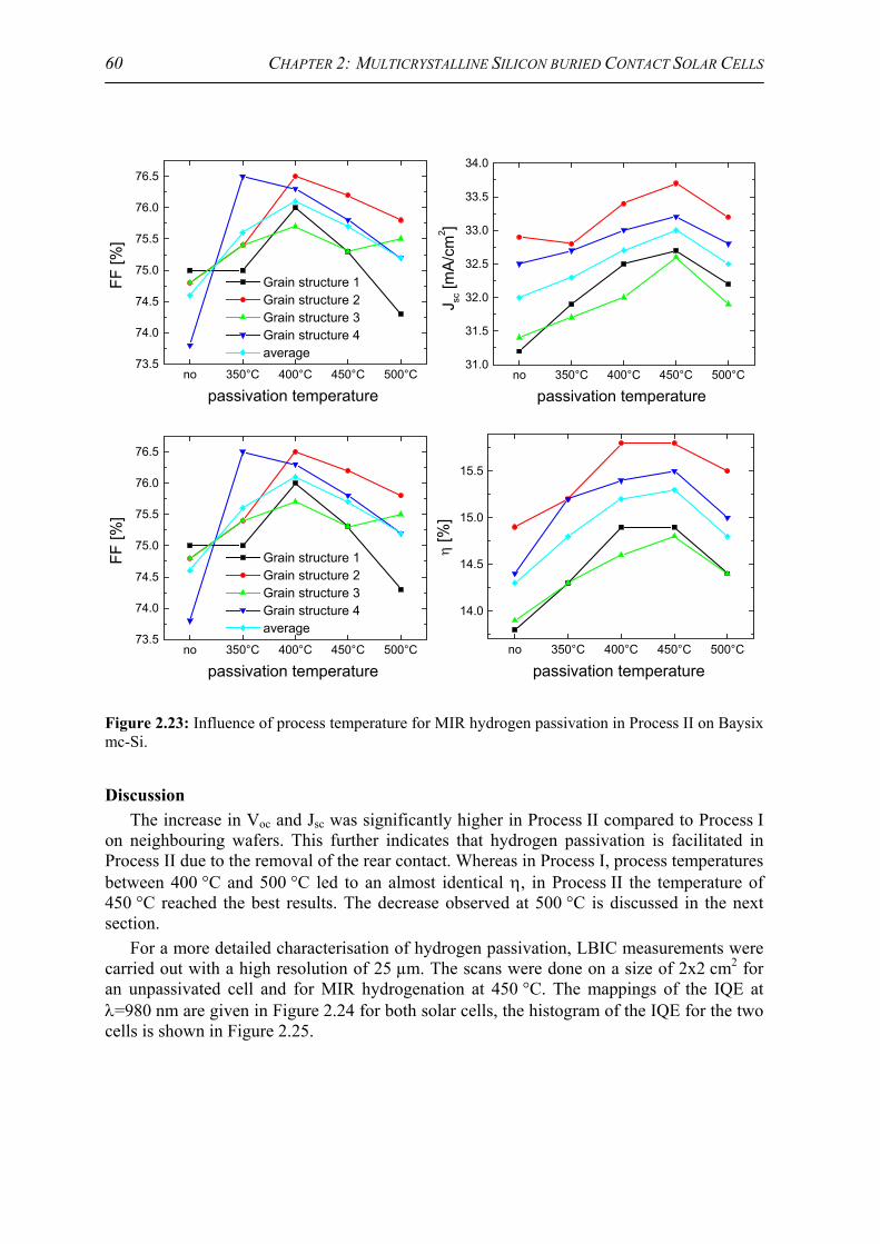
CHAPTER 2: MULTICRYSTALLINE SILICON BURIED CONTACT SOLAR CELLS 60
no 350°C 400°C 450°C 500°C73.5
74.0
74.5
75.0
75.5
76.0
76.5
Grain structure 1 Grain structure 2 Grain structure 3 Grain structure 4 average
FF [%
]
passivation temperature no 350°C 400°C 450°C 500°C
31.0
31.5
32.0
32.5
33.0
33.5
34.0
J sc [m
A/cm
2 ]
passivation temperature
no 350°C 400°C 450°C 500°C73.5
74.0
74.5
75.0
75.5
76.0
76.5
Grain structure 1 Grain structure 2 Grain structure 3 Grain structure 4 average
FF [%
]
passivation temperature no 350°C 400°C 450°C 500°C
14.0
14.5
15.0
15.5
η [%
]
passivation temperature
Figure 2.23: Influence of process temperature for MIR hydrogen passivation in Process II on Baysix mc-Si.
Discussion
The increase in Voc and Jsc was significantly higher in Process II compared to Process I on neighbouring wafers. This further indicates that hydrogen passivation is facilitated in Process II due to the removal of the rear contact. Whereas in Process I, process temperatures between 400 °C and 500 °C led to an almost identical η, in Process II the temperature of 450 °C reached the best results. The decrease observed at 500 °C is discussed in the next section.
For a more detailed characterisation of hydrogen passivation, LBIC measurements were carried out with a high resolution of 25 µm. The scans were done on a size of 2x2 cm2 for an unpassivated cell and for MIR hydrogenation at 450 °C. The mappings of the IQE at λ=980 nm are given in Figure 2.24 for both solar cells, the histogram of the IQE for the two cells is shown in Figure 2.25.

CHAPTER 2: MULTICRYSTALLINE SILICON BURIED CONTACT SOLAR CELLS 61
Figure 2.24: Spatially resolved measurements of the Internal Quantum Efficiency (IQE) at λ=980 nm determined by local LBIC and reflectivity measurements. (left) Unpassivated and (right) MIR hydrogen passivation at 450 °C for 120 min. A picture of the solar cell is shown in the middle indicating the crystal grain structure.
The LBIC-mapping shows that regions with an IQE below 0.4, corresponding to low
lifetime regions in the vicinity of crystal defects, are reduced for the passivated cell compared to the unpassivated one. Hence, the recombination activity of crystal defects is lowered. From the LBIC-mappings it can also be concluded that hydrogen diffusion through the contact groove is of minor importance. If a strong effect of in-diffusion through the contact grooves would occur, one expects, that the recombination of grain boundaries in the vicinity of the grooves is significantly reduced. However, this effect can not be observed.
Besides the passivation of the low lifetime regions, also the peak value of the IQE corresponding to high lifetime regions is reduced for the passivated cell. One possible explanation could be an inhomogenous Al-alloying with a higher SB. This seems rather unlikely, since the same process parameters for screen printing and firing were applied. Fischer observed [Fis02c] that τB is reduced, if a test sample with screen printed Al-BSF and removed Al rear contact is subjected to an additional treatment at 450 °C for 1 h. He suggests, that fast diffusing metallic impurities are inserted into the wafer and/or into the highly doped p+-region during contact firing which diffuse deeply into the wafer during subsequent annealing steps, even at moderate process temperatures of 450 °C. This effect could also explain the lower gain for hydrogen passivation at a process temperature of 500 °C.
However, still an average gain in η of 1%abs. was achieved due to hydrogen passivation at 450 °C. The lifetime reduction in the good grains due to metallic poisoning can be reduced by lowering the passivation time. A time of 90 min was sufficient for Process I, and a further reduction seems feasible for Process II due to the facilitated diffusion of hydrogen through the rear surface.
A picture taken from the corresponding section of the LBIC mappings shows a large quantity of crystal defects, whereas in the LBIC-scans only a reduced number is visible. This indicates that crystal defects have a different recombination strength, depending on the decoration with impurities like oxygen and metals [Law00].

CHAPTER 2: MULTICRYSTALLINE SILICON BURIED CONTACT SOLAR CELLS 62
0.1 0.2 0.3 0.4 0.5 0.6 0.7 0.8 0.90
100
200
300
400
500
with MIRHP hydrogenation without hydrogenation
coun
ts [a
.u]
IQE
Figure 2.25: Histogram of the IQE from the mappings in Figure 2.24.
Eurosil
The results of the illuminated IV-measurements on Eurosil are illustrated in Figure 2.26. For the average values the following can be observed: • Optimum process temperature is 450 °C. At this temperature, the best values of Voc, Jsc
and η are obtained. • The gain at this temperature is around ∆Voc=6 mV (1.0% rel.), ∆Jsc=0.4 mA/cm2
(1.2% rel.), and ∆η=0.4%abs. (2.8% rel.). The increase in η due to hydrogenation was lower for Eurosil than for Baysix. Also Spiegel observed, that the efficiency of MIR hydrogenation is reduced for Eurosil compared to Baysix [Spi98]. Therefore the two mc-Si materials respond differently to bulk passivation treatments. Whereas bulk passivation by P-gettering was very effective for Eurosil, hydrogenation was more effective for Baysix. Hence, the bulk lifetime is limited by different recombination centres. For Baysix, the defects can be passivated by hydrogen (e.g. decorated defects at dislocations and grain boundaries) whereas the removal of metallic impurities by gettering is the most successful technique on Eurosil.
2.8.5 Comparison of hydrogenation by MIR passivation and PECVD silicon nitride layers
The previous experiments showed that bulk passivation by the MIRHP-technique enhanced the solar cell efficiency of mc-Si BCSC. The remaining question is the effectiveness of this approach if compared to other techniques. The hydrogenation effect of PECVD SiNx films is very high if it is performed with the alloying of the rear contact in the processing of screen printed solar cells [Yel00]. As already mentioned, the application of this technique to BCSCs is rather doubtful. Thus, the comparative hydrogenation from PECVD-SiNx films was carried out on screen printed solar cells.

CHAPTER 2: MULTICRYSTALLINE SILICON BURIED CONTACT SOLAR CELLS 63
no 350°C 400°C 450°C 500°C575
580
585
590
595
600
605
V oc [m
V]
passivation temperature no 350°C 400°C 450°C 500°C
32.5
33.0
33.5
34.0
J sc [m
A/cm
2 ]
passivation temperature
no 350°C 400°C 450°C 500°C72.5
73.0
73.5
74.0
74.5
75.0
75.5
Grain structure 1 Grain structure 2 Grain structure 3 Grain structure 4 average
FF [%
]
passivation temperature no 350°C 400°C 450°C 500°C
14.0
14.2
14.4
14.6
14.8
15.0
15.2η
[%]
passivation temperature
Figure 2.26: Investigation on the influence of process temperature for MIR hydrogen passivation in Process II using Eurosil mc-Si.
Experiment
For the experiment, Baysix wafers were selected from the bottom, middle and top region of the same brick. The grain size of the material was large for wafers from the middle, medium for wafers from the top and small for wafers from the bottom. From the wafers, the bulk resistivity as well as the density of oxygen and carbon were determined [Rob00a] and are given in Table 2-9.
Table 2-9: Specific resistivity ρ, density of interstitial oxygen Oi and substitutional carbon Cs of Baysix mc-Si taken from different positions within the brick [Rob00a]. The bulk resistivity decreases from the bottom to the top due to the segregation coefficient of boron. The oxygen concentration is higher in the bottom due to contamination from the crucible walls.
ingot position ρ [Ωcm] Oi [1017 cm-3] Cs [1017 cm-3]bottom 1.4 3.6 0.5 middle 1.2 0.4 1.1
top 1.0 0.5 2.4

CHAPTER 2: MULTICRYSTALLINE SILICON BURIED CONTACT SOLAR CELLS 64
Three different processes were applied. The first one was Process II (see Figure 2.20) without hydrogen passivation and front surface texturisation. The second one included hydrogen passivation in the MIRHP-reactor (450 °C, 120 min). The third one was a standard process for screen printed solar cells as described in Figure 2.27.
edge isolation by mechanical dicing
co-firing of contactsin belt furnace
screen printing of front and rear contact
PECVD SiNx deposition
POCl emitter diffusion
saw damage removal +wafer cleaning
3
Figure 2.27: Processing sequence of screen printed solar cells with hydrogenation by firing-through PECVD SiNx during contact co-firing.
In the processing of screen printed cells, the as-cut saw damage was removed in hot NaOH (8-10 µm) followed by wafer cleaning in HCl and HF. Emitter diffusion was carried out using a POCl3-source (Rsheet=35 Ω/sqr). The diffusion glass was removed in diluted HF prior to the deposition of PECVD-SiNx using a direct plasma reactor. Thick film metal pastes were deposited by screen printing on the front (Ag) and rear (Al)3. During the co-firing in a belt furnace, the contact to the silicon wafer is formed and hydrogenation is accomplished. Edge isolation was carried out by mechanical dicing and cleaving leading to a solar cell area of 151 cm2. Further information about the manufacturing process for solar cells applying thick film metallisation at UKN can be found in [Ger02a] and [Hus02].
Results and discussion
IV and spectral response measurements Voc and Jsc are illustrated for the three processes in Figure 2.28. The effective bulk
diffusion lengths Leff were determined from a spectral analysis of the IQE and are also given in Figure 2.28.
3 Parts of the processing including screen printing was carried out by F. Huster.
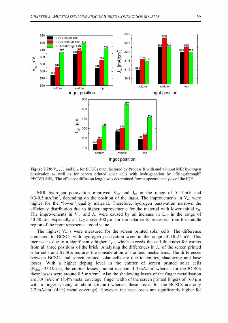
CHAPTER 2: MULTICRYSTALLINE SILICON BURIED CONTACT SOLAR CELLS 65
bottom middle top560
570
580
590
600
610
620
630
612
596
585
619
609604
607
586
575
V oc [m
V]
ingot position
BCSC, no MIRHP BCSC, with MIRHP SP, fire-through SiN
bottom middle top
30.5
31.0
31.5
32.0
32.5
33.0
32.0
32.3
32.0
32.3
32.8
32.3
31.531.6
31.0
J sc [m
A/cm
2 ]
ingot position
bottom middle top
100
200
300
400
500
600
140
190
325
270310
190230
415
550
L eff [
µm]
ingot position Figure 2.28: Voc, Jsc and Leff for BCSCs manufactured by Process II with and without MIR hydrogen passivation as well as for screen printed solar cells with hydrogenation by “firing-through” PECVD SiNx. The effective diffusion length was determined from a spectral analysis of the IQE.
MIR hydrogen passivation improved Voc and Jsc in the range of 5-11 mV and
0.3-0.5 mA/cm2, depending on the position of the ingot. The improvements in Voc were higher for the “lower” quality material. Therefore, hydrogen passivation narrows the efficiency distribution due to higher improvements for the material with lower initial τB. The improvements in Voc and Jsc were caused by an increase in Leff in the range of 40-50 µm. Especially an Leff above 300 µm for the solar cells processed from the middle region of the ingot represents a good value.
The highest Voc´s were measured for the screen printed solar cells. The difference compared to BCSCs with hydrogen passivation were in the range of 10-21 mV. This increase is due to a significantly higher Leff, which exceeds the cell thickness for wafers from all three positions of the brick. Analysing the differences in Jsc of the screen printed solar cells and BCSCs requires the consideration of the loss mechanisms. The differences between BCSCs and screen printed solar cells are due to emitter, shadowing and base losses. With a higher doping level in the emitter of screen printed solar cells (Rsheet=35 Ω/sqr), the emitter losses amount to about 1.3 mA/cm2 whereas for the BCSCs these losses were around 0.5 mA/cm2. Also the shadowing losses of the finger metallisation are 3.9 mA/cm2 (8.4% metal coverage, finger width of the screen printed fingers of 160 µm with a finger spacing of about 2.6 mm) whereas these losses for the BCSCs are only 2.2 mA/cm2 (4.9% metal coverage). However, the base losses are significantly higher for

CHAPTER 2: MULTICRYSTALLINE SILICON BURIED CONTACT SOLAR CELLS 66
BCSCs due to the lower Leff. Despite the higher base losses, Jsc is higher for BCSCs with hydrogenation compared to screen printed cells due to lower emitter and shadowing losses.
LBIC scans and spatial distribution of the IQE
For a local characterisation, LBIC scans were carried out for the cells from the top region of the ingot. The result of the LBIC scans are shown as local IQE-mapping at λ=980 nm for the three different processes in Figure 2.29. For a facilitated quantitative comparison a histogram of the IQE is given in Figure 2.29.
For the unpassivated BCSC, a large fraction of the wafer area has a low IQE below 0.5. The corresponding Leff in these regions is around 60 to 100 µm. Most of the very poor regions were passivated during MIR hydrogenation, but still a large part of the cell has an IQE below 0.5. The hydrogen passivation in the “firing-through” process led to improvements in the “good” and “bad” grains leading to a narrow distribution. The regions with an IQE below 0.5 nearly vanished for the screen printed solar cells.
The experiments showed, that bulk passivation by hydrogenation from a PECVD SiNx film is more effective. It was shown in [Yel00] that the very effective hydrogenation is due to a synergetic effect including the presence of Al, high process temperatures reached during screen printing and a hydrogen-rich PECVD SiNx layer. In their study they observed that a very effective hydrogenation requires the presence of Al as well as process temperatures of around 850 °C. Annealing of the PECVD SiNx film without Al led to significantly lower improvements in the bulk lifetime. They proposed a three step model to explain the effective hydrogenation with the following parameters:
(1) release of hydrogen from the PECVD SiNx layer (2) injection of vacancies generated during the alloying process (3) retention of hydrogen at the passivating sites The injected vacancies dissociate hydrogen molecules and support the hydrogen
diffusion into the wafer. In the MIRHP process, vacancies are not present to facilitate the diffusion which is one explanation for the superiority of the “firing-through” process.
Another major difference between the MIR hydrogen passivation of BCSCs and the “firing-through” PECVD SiNx process is the location of the “hydrogen source” or location of in-diffusion. In the firing-through process, hydrogen is incorporated at the front surface, in the MIR process from the rear. The hydrogen has to diffuse throughout the wafer to passivate defects in the front surface region.
At this point, it is not clear if the synergetic effect or the location of the hydrogen source is the reason for the reduced hydrogenation of the MIRHP-technique in BCSC processing. To clarify this, further investigations are necessary.

CHAPTER 2: MULTICRYSTALLINE SILICON BURIED CONTACT SOLAR CELLS 67
0.2 0.3 0.4 0.5 0.6 0.7 0.8 0.9 1.00
20
40
60
80
100
120
140
160
BCSC, no MIRHP BCSC, with MIRHP SP, firing through SiN
coun
ts [a
.u.]
IQE
Figure 2.29: Local IQE at λ=980 nm determined from LBIC and reflectivity measurements for (top, left) BCSC without hydrogen passivation (top, right) BCSC with MIR hydrogen passivation and (bottom, left) screen printed solar cell with hydrogenation from a PECVD SiNx layer. (bottom, right) histogram of the IQE.

CHAPTER 2: MULTICRYSTALLINE SILICON BURIED CONTACT SOLAR CELLS 68
2.9 Summary
In this Chapter two processing sequences for Buried Contact Solar Cells (BCSCs) on multicrystalline silicon (mc-Si) were investigated. In Process I the rear surface is passivated by a thin evaporated Back Surface Field (BSF) and it includes P-Al co-diffusion/gettering. Screen printing of Al pastes was applied in Process II to enhance the thickness of the BSF thereby reducing rear surface recombination.
In section 3, mechanical V-texturing was investigated applying single blade texturing or a texturing wheel. The improvements in Jsc due to the reduction of front surface reflection and the enhancement of charge carrier collection in the macroscopic V-texture was quantified. Additional effects applying for mechanically V-textured cells with the specific design of this work were discussed, namely the reduction of the series resistance and possible increases in the dark saturation current densities. Mechanical V-grooving using a texturing wheel increased Jsc by 1.5 mA/cm2 and η by 0.7% abs.
The presence of crystal defects and metallic impurities reduces the bulk diffusion length of the as-grown wafer. To enhance LB during solar cell processing, gettering as well as hydrogenation was introduced in the processing sequence. Gettering of metallic impurities was investigated in section 4 by treatments including P and Al. P-gettering led to a doubling of the bulk lifetime τB for Eurosil mc-Si. A slight reduction in τB was observed for Polix and Baysix during P-diffusions at high process temperatures. The investigations on different temperatures of Al-gettering and P-Al co-gettering on Eurosil and Baysix revealed, that the optimum gettering efficiency is accomplished by co-gettering at a process temperature of 950 °C for both materials.
The incorporation of hydrogen passivation was investigated in section 5 by a remote hydrogen plasma source using the MIRHP-technique. The improvements in solar cell efficiency depended on the material quality and were in the range of 0.4% to 1.7% abs. The MIR hydrogen passivation was optimised for Process I with respect to temperature and duration. The highest improvements in η have been observed for temperatures in the range of 400-500 °C and for process times between 90 and 120 min.
The investigations for Process I were continued in section 6 with the manufacturing of a larger batch on a wafer size of 12.5x12.5 cm2. The average efficiency was 15.7% for 36 cells, which were used for the fabrication of a module with a power of 81.1 Wp. The highest efficiency in this experiment and for Process I was 16.0%. The loss analysis revealed that the efficiency was mainly limited by the rudimentary rear surface passivation of several thousand cm/s which led to the development of Process II.
This process was investigated in section 8. The increase in Voc of 10 mV and Jsc of 0.9 mA/cm2 for Process II compared to Process I was due to improved rear surface passivation and facilitated hydrogen in-diffusion through the rear surface. For MIR hydrogen passivation an optimum process temperature of 450 °C was determined, which led to an average increase in efficiency of 1.0%abs. on Baysix and 0.4%abs. on Eurosil.
The effectiveness of MIR hydrogenation in the BCSC process was compared to hydrogenation in the “firing-through” PECVD SiNx process of screen printed solar cells. Wafers were selected from three different positions within one brick. MIR hydrogen passivation improved Voc by 5-11 mV and Jsc by 0.3-0.5 mA/cm2 due to an increase in Leff of 40-50 µm. Hydrogenation in the “firing-through” PECVD SiNx process was more effective leading to higher Voc’s and effective bulk diffusion lengths.

69
3 Highly Efficient Large Area Buried Contact Solar Cells on Multicrystalline Silicon
The first section of this Chapter reviews the processing of highly efficient solar cells on multicrystalline silicon (mc-Si), both on small laboratory cell areas and on larger industrial type cell sizes. The investigations on mc-Si solar cells in the previous Chapter led to the development of a processing sequence with front surface texturing and bulk as well as surface passivation. In this Chapter, the processing of highly efficient large area BCSCs is described and the cells are characterised. Based on a loss analysis, suggestions for further efficiency improvements are made.
3.1 State-of-the-art
In the last years many investigations were carried out to increase the solar cell efficiency of mc-Si solar cells (see Table 3-1). The highest efficiency achieved so far is η=19.8 % on a cell area of 1 cm2 by Zhao et al. [Zha98] at the University of New South Wales, Australia. This high efficiency was obtained on Eurosil mc-Si applying the PERL (Passivated Emitter Rear Locally-diffused) design developed for highly efficient monocrystalline silicon cells. The front surface was “honeycomb” textured which is accomplished by isotropic etching through regular openings in a dielectric masking layer. The deposition of a double layer ARC further reduced front surface reflectance. The high solar cell efficiency was possible, since this specific mc-Si material was tolerant to high temperature processing. Process temperatures exceeding 1000 °C have been applied for boron diffusions as well as for the growth of high quality oxides. The authors attributed the tolerance to high temperature processing to modifications of the directional solidification growth process at Eurosolare [Fer98]. The specific nature of mc-Si with (strong) local variations in bulk lifetime is not taken into account if solar cells are processed on small areas. Efficiencies as low as 13.5% have been reported by the authors on the same wafer in an area with a higher defect density. Processing of high efficiency solar cells on small areas can demonstrate the potential of a

CHAPTER 3: HIGHLY EFFICIENT LARGE AREA BCSCS ON MULTICRYSTALLINE SILICON 70
process if mc-Si material quality is improved in future. However, processing of large area solar cells is unavoidable to identify the real potential of current mc-Si materials.
The second highest efficiency reported is 18.6 % on a cell area of 1 cm2 using HEM material [Roh96]. The process involved P-gettering and the evaporation of a thick Al layer (10 µm) for a full area Al-BSF. The metallisation was formed by photolithography and lift-off techniques. The front surface was untextured but a double layer ARC was deposited.
Two Japanese companies reported high efficiencies on large area solar cells already in the nineties. Sharp obtained a solar cell efficiency of 17.2 % on casted mc-Si from Sumitomo SiTiX on a cell area of 10x10 cm2 [Nak94]. They applied front surface texturing by mechanical V-grooving with bevelled dicing blades similar to the approach in this work. Surface passivation was achieved by a thin thermal oxide on the front and by a full area BSF on the rear. The front surface was additionally coated by a double layer ARC (TiO2/MgF2) and metallisation was performed by screen printing. Bulk passivation by hydrogenation was not reported in their work.
An efficiency of 17.1 % was reported by Kyocera for ElectroMagnetically Casted (EMC) mc-Si from Sumitomo Sitix on a cell area of 15x15 cm2 [Fuk97], [Shi97]. They applied Reactive Ion Etching (RIE) for front surface texturing as well as Plasma Enhanced CVD SiNx on front and rear for hydrogen passivation. Additional features are local contacting through the PECVD SiNx layer on the rear to the Al-BSF underneath the SiNx as well as SiNx as single layer ARC. Front contact formation was performed by lift-off techniques which is currently not considered as low-cost approach.
Table 3-1: Overview of best solar cell efficiencies on mc-Si for different substrate sizes.
mc-Si material and manufacturer
efficiency / area [cm2]
institute / company [reference]
basic features of device design and processes
Eurosil / Eurosolare 19.8 % /1 cm2 UNSW [Zha98] PERL, honeycomb texture, PL, DLARC
HEM / Crystal systems 18.6 % / 1 cm2 Georgia Tech [Roh96]
P-gettering, PL, DL ARC
DS/ Sumitomo SiTIX 17.2 %/ 100 cm2 Sharp [Nak94] V-texture, DL ARC, screen printing
DS/ Sumitomo SiTIX 17.1 % / 225 cm2 Kyocera [Fuk97] RIE, local contacts, hydrogenation, lift-off
3.2 Solar cell processing
Two different materials were used for the processing of highly efficient BCSCs. The first one was Baysix from the middle region of the brick which was also used for the experiments in the last section of Chapter 2 (wafer size 12.5x12.5 cm2, ρ=0.8-1.2 Ωcm, initial thickness 330 µm). The second one was Polix from Photowatt (wafer size 12.5x12.5 cm2, ρ=0.5 Ωcm, initial thickness 350 µm). The processing sequence is given in Figure 3.1 and is very similar to the sequence described in the last section in Chapter 2. Only the differences will be described in the following.

CHAPTER 3: HIGHLY EFFICIENT LARGE AREA BCSCS ON MULTICRYSTALLINE SILICON 71
Mechanical V-texturing using the single blade technique (angle of 60 ° at the V-tips) was applied since this approach leads to the best performance with respect to the reduction of reflection losses (see Chapter 2). The depth of the grooves was about 70 to 80 µm, the distance between the grooves about 100 µm. The low curvature radius in the grooves ensures a low front surface reflectance compared to wheel textured cells [Zec99]. The saw damage was removed in an acidic solution. For etching a modified CP 6 solution was used containing HF (50 %) – HNO3 (65 %) – CH3COOH (100 %) in the ratio of 3:43:7 with an isotropic etching rate of 0.65 µm/min. The removed silicon material was about 3-4 µm. Isotropic etching solutions maintain the high quality of the mechanically V-textured front surface. Alkaline etching solutions with its anisotropic etching behaviour might lead to a non-optimum geometry within the bottom of the V-grooves enhancing the front surface reflectance [Ger02b]. Another difference to the standard sequence was an unintended lower emitter sheet resistance of 70-80 Ω/sqr instead of 100 Ω/sqr at the end of the process. Edge isolation was performed by mechanical dicing and cleaving removing 2.5 mm from the wafer edge. The resulting solar cell area was 144 cm2. Due to wafer breakage, the area was only 119 cm2 for the best Baysix cell. After edge isolation the busbars were tabbed using 1 mm wide Cu ribbons.
Al evaporation (<1µm) + electroless Ni/Cu plating + edge isolation
MIR hydrogen passivation450°C, 2h
screen printing of Al + firing + removal of contact in HCl
POCl3 groove diffusion950°C, 30 min
NaOH defect etch +HCl + HF
mechanical contact groove formation
LPCVD SiNx deposition
POCl3 emitter diffusion 100 Ω/sqr
acidic defect etch +HCl + HF
mechanical V-texturing applying the single blade technique
Figure 3.1: Processing sequence for the fabrication of highly efficient BCSCs on mc-Si (Process II). Front surface texturing is carried out by mechanical V-grooving applying the single blade approach. Bulk passivation by hydrogenation is done in a MIRHP-reactor.

CHAPTER 3: HIGHLY EFFICIENT LARGE AREA BCSCS ON MULTICRYSTALLINE SILICON 72
3.3 Characterisation
3.3.1 Illuminated IV characteristics
The parameters of the illuminated IV-measurements are given in Table 3-2 for the best solar cells. For the two solar cells on Polix, efficiencies of 17.5 % and 17.4 % were achieved. The IV-parameters of Polix 1 with an efficiency of 17.5 % were independently confirmed at the callab of FhG-ISE, Germany. The illuminated IV-characteristic as measured at FhG-ISE callab under standard test conditions (AM1.5, 1000 W/m2, T=25 °C) is given in Figure 3.2. An efficiency of 17.5 % is to the knowledge of the author the highest efficiency obtained on a cell area equal or larger than 100 cm2 up to now on mc-Si. A very high Voc of 628 mV and Jsc of 36.3 mA/cm2 were determined, which are amongst the highest values obtained for large area mc-Si solar cells. The front surface is only coated with a single layer ARC allowing a further increase in Jsc by the deposition of a second ARC. The fill factor of 76.9 % is rather moderate. Also a good efficiency was obtained on Baysix with η=16.5 %. A similar Jsc was measured with 36.0 mA/cm2 indicating that Leff is similar to Polix, whereas mainly due to a lower doping level a reduced Voc of 603 mV was obtained. A detailed analysis of these cells is performed in the next sections.
Table 3-2: Illuminated IV-parameters for BCSCs on Polix and Baysix mc-Si processed according to the sequence given in Figure 3.1. Cell area 144 cm2 for Polix and 119 cm2 for Baysix. *Independently confirmed at FhG-ISE, Freiburg.
Mc-Si Voc [mV]
Jsc [mA/cm2]
FF [%]
η [%]
Polix 1 628 36.3 76.8 17.5* Polix 2 626 36.2 76.9 17.4 Baysix 603 36.0 76.1 16.5
Figure 3.2: Illuminated IV-characteristic and IV-parameters for Polix 1 as measured at FhG-ISE callab.

CHAPTER 3: HIGHLY EFFICIENT LARGE AREA BCSCS ON MULTICRYSTALLINE SILICON 73
3.3.2 Dark IV and Jsc-Voc characteristics
The dark IV- and Jsc-Voc-characteristics were measured to extract the parameters of the Two-Diode model. The results are given in Table 3-3, in Figure 3.3 the measured as well as fitted Jsc-Voc curves for Polix 1 and Baysix are shown.
Table 3-3: Diode parameters determined from a fit of the Two-Diode model to the dark, illuminated and Jsc-Voc curve. The number in italics for Rsh is determined in the negative range, the other one from the Jsc-Voc curve leaving Rsh as parameter.
Mc-Si J01 [10-12A/cm2]
J02 [10-8A/cm2]
Rsh [Ωcm2]
Rs [Ωcm2]
Polix 1 0.76 3.6 1600/2900 0.62 Polix 2 0.82 3.6 1600/3000 0.57 Baysix 1.9 6.6 8000 0.62
0.30 0.35 0.40 0.45 0.50 0.55 0.600.01
0.1
1
10
100
Vmpp
Vmpp
n=2
n=1
measured Jsc- Voc, Polix 1 fitted, Polix 1 measured Jsc- Voc, Baysix fitted, Baysix
J sc [m
A/cm
2 ]
Voc [V] Figure 3.3: Measured Jsc-Voc and fitted curves for Polix 1 and Baysix. The parameters extracted from the fit with n1=1 and n2=2 are given in Table 3-3. The red and black line represent the voltage at maximum power point Vmpp.
Discussion
The high Voc of 628 mV for Polix 1 is due to a low saturation current density of the first diode J01. The low J01 follows from a relatively high base doping level and a good effective bulk diffusion length Leff exceeding the cell thickness (see next section). For Baysix, Leff was in the same range, but the base doping was lower leading to a higher J01 and therefore lower Voc compared to Polix.
For Baysix a high shunt resistance Rsh of 8000 Ωcm2 was measured which will not negatively influence the fill factor. For Polix 1 Rsh determined in the negative voltage range was 2900 Ωcm2, which represents also a sufficiently high value. However, under forward bias, an increase in the current is observed for lower voltages, which can be described by

CHAPTER 3: HIGHLY EFFICIENT LARGE AREA BCSCS ON MULTICRYSTALLINE SILICON 74
decreasing Rsh to about 1600 Ωcm2. In general, the excess current in this voltage range is difficult to attribute to either J02 or a “classical” shunt resistance. The curve can also be fitted by taking the shunt value in the dark voltage range and include n2 as fitting parameter. In this case, J02 will be 2x10⁻⁶ A/cm2 and n2=3.3. The problem can therefore be described in different ways but the net effect is the same: an additional current flows at lower voltages reduceing the fill factor and therefore solar cell efficiency. This increase in current is very pronounced for voltages up to 0.45 V for Polix 1 (see Figure 3.3). A similar effect was not observed on Baysix mc-Si throughout this work suggesting that it could be specific to this Polix mc-Si material and is therefore not related to the processing or solar cell metallisation. This kind of “shunting” behaviour is sometimes attributed to the “bad” regions in wafers which might be caused by dissolved metallic precipitates. An LBIC scan (see Figure 3.6) shows some regions with a low lifetime which could cause this local “shunting”. A shunt resistance of 1600 Ωcm2 reduces the fill factor for Polix 1 from 77.5 % (Rsh=10000 Ωcm2) to 76.8 %.
For Baysix, J02 was determined to 6.6x10⁻⁸ A/cm2. The curve could be fitted by taking Rsh from negative voltages and keeping n2=2. Besides a minor reduction in Voc, J02 mostly reduces the fill factor as can be seen in the Jsc-Voc curve. At the maximum power point , the slope has already a large deviation from its ideal value of n=1 and therefore indicates the influence of J02. As already discussed in Chapter 2, the higher J02 compared to mono-Si is most probably caused by defects in the space charge region.
The series resistance Rs was in the range of 0.6 Ωcm2, which is a reasonably low value for large area industrial solar cells indicating the high quality front side metallisation of BCSCs. However, it has to be noted that the FF directly after completion of the solar cell process and busbar tabbing was measured in the range of 77.5 to 77.8 %. The independent confirmation at FhG-ISE was several weeks afterwards and led to a fill factor of 76.9 %. Re-measuring the solar cell at UKN after this period, also a FF was measured similar to the one at FhG-ISE callab. The analysis of the corresponding illuminated IV-curve revealed that this was caused by an increase in Rs from 0.43 Ωcm2 to 0.62 Ωcm2. The effect of a higher Rs is most probably associated with an increase in the line resistance of the contact fingers. The reason of this increase is not clear at the moment.
3.3.3 Spectral analysis
The Internal Quantum Efficiency (IQE), External Quantum Efficiency (EQE) and reflectivity for Polix 1 is shown in Figure 3.4 and for Baysix in Figure 3.5. The very low reflectivity demonstrates the high quality of V-texturing applying the single blade approach with a weighted reflectance of 4.7 % on the unmetallised part. The high IQE in the long wavelength range indicates a high Leff for both materials. Leff is well above 400 µm as determined by a spectral analysis on neighbouring untextured Baysix cells. The IQE in the short wavelength range was reduced compared to other BCSCs in this work leading to higher emitter losses (see next section).

CHAPTER 3: HIGHLY EFFICIENT LARGE AREA BCSCS ON MULTICRYSTALLINE SILICON 75
400 500 600 700 800 900 1000 1100 12000
20
40
60
80
100
IQE EQE REF
IQE
, EQ
E, R
EF
[%]
λ [nm] Figure 3.4: Internal Quantum Efficiency (IQE), External Quantum Efficiency (EQE) and reflectivity of Polix 1.
400 500 600 700 800 900 1000 1100 12000
20
40
60
80
100
IQE EQE REF
IQE
, EQ
E, R
EF
[%]
λ [nm] Figure 3.5: Internal Quantum Efficiency (IQE), External Quantum Efficiency (EQE) and reflectivity of Baysix.
Local LBIC and reflectivity measurements were carried out on Polix 1 and are given as
IQE-mapping at λ=980 nm in Figure 3.6. The LBIC scan shows the excellent homogeneity of the material with only a small number of grains with a low IQE. However, these grains could be responsible for the non-ideal diode behaviour at low voltages as discussed in the previous section.

CHAPTER 3: HIGHLY EFFICIENT LARGE AREA BCSCS ON MULTICRYSTALLINE SILICON 76
Figure 3.6: IQE mapping at λ=980 nm obtained from local LBIC and reflectivity measurements for Polix 1
3.3.4 Loss analysis
In the following, a loss analysis is carried out for the Polix and Baysix cells. In general the losses can be divided in • optical • resistive • recombination
The determination of the optical and recombination losses are performed using an evaluation of the IQE and reflectivity measurements as described in [Fis02d]. The resistive losses were already discussed in the previous section. The results of the determination of the recombination and optical losses are given in Table 3-4.
Table 3-4: Optical and recombination losses for the three investigated solar cells (in mA/cm2). Jsc (SR) denotes the short circuit current density as determined from the spectral response measurement, which was about 0.5-0.7 mA/cm2 higher as Jsc obtained from the illuminated IV-measurements.
Optical losses Recombination losses Solar cell Jsc (SR) shadowing reflection Emitter Base+ rear abs.Polix 1 37.0 1.84 1.76 0.67 4.62 Polix 2 37.0 1.84 1.80 0.55 4.70 Baysix 36.51 2.3 1.77 0.54 4.77

CHAPTER 3: HIGHLY EFFICIENT LARGE AREA BCSCS ON MULTICRYSTALLINE SILICON 77
The metal coverage on the front is 4.0 % (finger width 28 µm, finger spacing 1.4 mm and busbar width of 1 mm) for the two Polix cells and 6.0 % for the Baysix due to overplating at one wafer edge. A metal coverage of only 4 % is very low compared to screen printed solar cells (7-8 %). The front surface reflection losses on the unmetallised part amount to 1.8 mA/cm2 for all solar cells. Further reductions are expected by the deposition of a second layer ARC e.g. of MgF2.
The emitter losses are lowest for Baysix and highest for Polix 1. The rather high emitter losses for the Polix cells in the range of 0.6-0.7 mA/cm2 are caused by an unintended low emitter sheet resistance of 70-80 Ω/sqr. It was demonstrated in Chapter 2, that the optimised emitter as well as front surface passivation generally leads to losses in the range of 0.2-0.3 mA/cm2. Hence a significant improvement in Jsc can be achieved if process inhomogeneities leading to variations in Rsheet are avoided. Base recombination, which includes absorption in the rear contact, is in the range between 4.5-4.9 mA/cm2.
3.3.5 Potential for further efficiency improvements in Process II
Based on the solar cell parameters of Polix 1 and on the results of the loss analysis, the potential for a higher solar cell efficiency for Process II is investigated. The results are shown in Table 3-5.
Table 3-5: Possibilities for a further increase in solar cell efficiency by omitting processing as well as material inhomogeneities.
Voc [mV]
Jsc [mA/cm2]
FF [%]
η [%]
Polix 1, as measured 628 36.3 76.8 17.5 Reduction in emitter losses by avoiding process inhomogeneities, +0.5 mA/cm2
628.5 36.8 76.8 17.8
Enhance shunt to Rsh>10000 Ωcm2 628.8 36.8 77.5 17.9 Reduction of Rs to 0.42 Ωcm2 as determined after plating
628.8 36.8 77.8 18.0
The highest increase in solar cell efficiency can be accomplished by the reduction of the emitter losses. If the emitter losses are reduced by 0.5 mA/cm2 an efficiency of 17.8 % can be achieved. A further increase up to 18.0 % is obtained by an increase in Rsh and by a reduction of Rs to the value demonstrated directly after solar cell processing of 0.42 Ωcm2. Hence, an efficiency of 18.0 % is possible with Process II in the near future.
Further efficiency improvements require additional process steps or an adaptation of the processing sequence. The deposition of a second ARC leads to a further increase in Jsc. Improvements can also be expected by enhanced bulk passivation e.g. by hydrogenation from PECVD SiNx films deposited at the rear surface followed by annealing as has already been proven its efficiency in [Fuk97]. Also an improved rear surface passivation e.g. by dielectric layers can increase the solar cell efficiency as well as a back surface reflector for enhanced light trapping. Some of these issues are currently investigated at our institute and will be applied to BCSCs in the near future in a continuation of this work in an EC funded project.

CHAPTER 3: HIGHLY EFFICIENT LARGE AREA BCSCS ON MULTICRYSTALLINE SILICON 78
Apart from single blade texturing, the applied processing sequence relied on industrial production techniques. Single blade texturing can be replaced by wheel-texturing which is applied at sunways AG for the fabrication of POWER solar cells [Fat00]. Wheel texturing reduces Jsc by about 0.9 mA/cm2 (see Chapter 2) corresponding to a loss in efficiency of about 2-3 % on solar cell level, which significantly reduces for encapsulated solar cells [Ger02a].
In this Chapter, a record high efficiency of 17.5 % for a large area multicrystalline silicon solar cell was obtained, which proofs the quality of the investigated processing sequence and of the BCSC technology, especially for high quality mc-Si materials.

79
4 Back Contact Silicon Solar Cells
Back contact solar cells are devices with emitter and base contacts located at the rear surface. The first part of this Chapter motivates the increasing interest on back contact solar cells and introduces different device designs. In the second section specific new process technologies for the fabrication of back contact solar cells are described. Processing, characterisation and simulation of three back contact solar cell designs made by electroless plating are described in the third and fourth section: the Metallisation Wrap Around (MWA), Metallisation Wrap Through (MWT) and Emitter Wrap Through (EWT) solar cells.
4.1 Device designs of back contact solar cells
Back contact solar cells have been investigated for many years with different device designs and for various applications. In the first part of this section a short overview is given on high efficiency back contact solar cells. Since low cost devices for applications in the mass market are investigated in this work, different designs of this category are described in the following.
4.1.1 High efficiency devices
In conventional solar cells, the metal coverage on the front side is a compromise between shadowing and series resistance losses. High efficiency back contact solar cells allow the decoupling of these two factors: the front surface is optimised for optical performance as well as low surface recombination and the rear surface for low series resistance losses. Therefore back contact solar cells are especially suitable for concentrator applications which require a low series resistance due to a high I2R power loss.
In general, high efficiency back contact solar cells have a collecting junction only on the rear surface whereas the front surface is well passivated (see Figure 4.1). The minority charge carriers mainly generated in the front surface region have to diffuse a long way to the

CHAPTER 4: BACK CONTACT SILICON SOLAR CELLS 80
rear junctions. Hence, these devices require a high ratio of bulk diffusion length to cell thickness.
The first design of an Interdigitated Back Contact (IBC) solar cell (see left picture in Figure 4.1) was investigated by Schwartz and Lammert [Schw75], [Lam77]. (For a review of the early research on back contact solar cells for concentrator applications see [Schw82]). Swanson reduced the rear surface recombination leading to the point-contact silicon solar cell (see right picture in Figure 4.1) [Swa84]. The manufacturing process for all of these devices were rather complex. Sinton [Sin90] introduced a simplified manufacturing process for the IBC cell design referred to as the trench mesa design. This process involves only one photolithography step and no alignment steps at all. SunPower Corp. [Ver94] and Amonix are currently commercialising IBC solar cells.
Figure 4.1: Schematic drawing of (left) Interdigitated Back Contact (IBC) solar cell [Schw82] and (left) point contact solar cell [Swa84].
4.1.2 Advantages of low cost back contact solar cells
The research on low cost approaches was motivated by several aspects. First of all, the device designs should lead to efficiencies in the range of conventional cells on materials with a lower bulk diffusion length. The technology involved in the processing of high efficiency back contact solar cells is too expensive to be produced for the mass market of one sun applications. In this work the term “low cost industrial type solar cells” is used for devices for which the costs per Wp are comparable to conventional industrial solar cells. The materials to be used for solar cell processing are the standard materials of the PV industry: solar grade Cz-Si and mc-Si.
The research on back contact solar cells is motivated by the following points: • Easier module assembly • High aesthetics • Potential for higher solar cell efficiency • Easier module assembly for thin solar cells with thickness well below 200 µm • Reduced series resistance for large area solar cells (>12.5x12.5 cm2)

CHAPTER 4: BACK CONTACT SILICON SOLAR CELLS 81
Easier module assembly and high aesthetics Currently, about 85% of the total PV-shipment consists of crystalline silicon solar cells
[Pho02]. In the modules the cells are interconnected in series with solder tabs running from the front to the rear surface of the next solar cells. These solder tabs need to be highly conductive for minimum series resistance losses and are therefore rather wide (around 1.5 to 2.5 mm). For architects these busbars are disturbing with respect to the optical appearance of PV modules. This point is especially important for building integrated PV which is a fast growing market segment in the current PV industry. By eliminating the busbar solder tabs or the complete metallisation on the front surface, this new generation of crystalline Si modules has a higher optical appearance and opens new markets for PV.
The above mentioned procedure for series interconnection of conventional solar cells has several disadvantages. The process itself is difficult to automate and therefore labour-intensive [Gee97]. The solder tabs will stress the wafer at the edges unless the cells are generously spaced. Back contact solar cells allow novel schemes for module interconnection (see section 5). Also back contact cells can be closer spaced allowing a higher packing density within the module.
Potential for higher solar cell efficiency Due to the reduction or even absence of grid shadowing losses the active light absorbing
front surface is increased. Some designs of back contact solar cells also have a large fraction of a second carrier collecting junction at the rear leading to higher currents densities. This is especially beneficial for crystalline silicon materials with a lower ratio of bulk diffusion length to cell thickness.
Advantages for future crystalline silicon modules: thinner wafers and larger substrates The induced stress at the wafer edges during module fabrication might be too high for
thin wafers leading to an enhanced breakage rate. If the wafer size is enhanced towards 15x15 cm2 or larger, very high currents above 8 A will be created under one sun illumination. Since these currents have to be transported in the busbar tabs, the series resistance loss I2R will be enhanced. The trade-off between resistive and optical shading losses in module fabrication is omitted for most back contact designs. In these designs, the high currents are transported in the interconnections on the rear which can be optimised for a low series resistance.
4.1.3 Device designs of low cost back contact solar cells
Metallisation Wrap Around Solar Cells MWA solar cells can be described as conventional cells in which the busbars on the
front are moved towards the edge regions on the rear surface (see Figure 4.2). In these devices there is still finger metallisation present on the front side. Compared to other rear contact solar cells, it is advantageous that these devices do not require holes or vias for the electrical interconnection of front and rear.
The main technological problems to be solved for MWA solar cells are: • Sufficient and reliable metal deposition at the edges • Contact separation of the p- and n-type regions on the rear
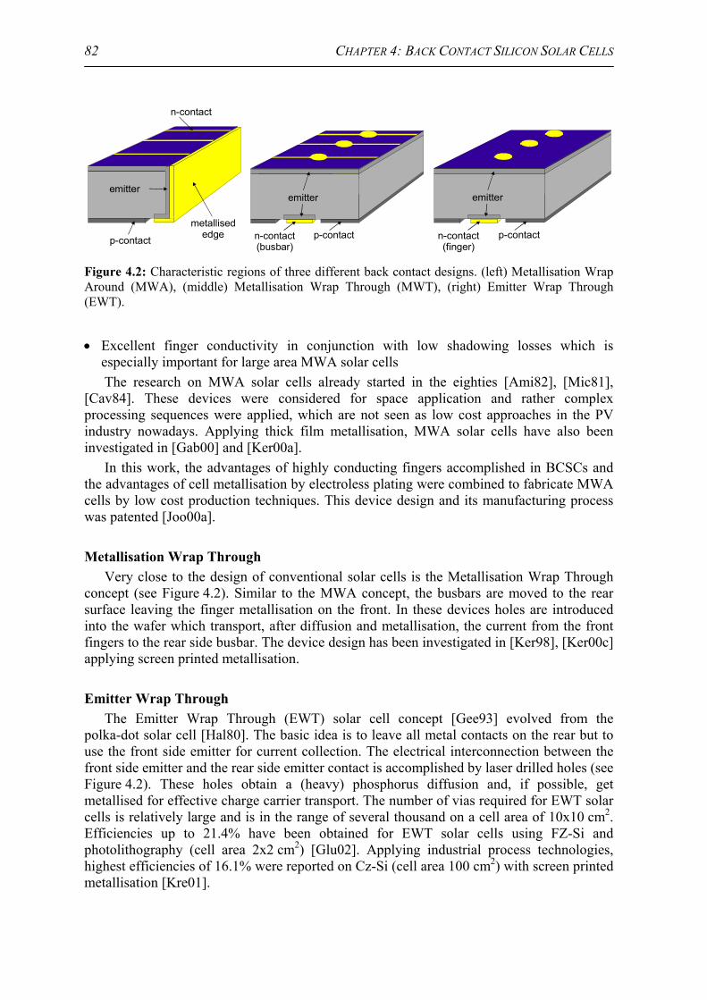
CHAPTER 4: BACK CONTACT SILICON SOLAR CELLS 82
p-contact
metallised edge
emitter
n-contact
emitter
p-contactn-contact(busbar)
emitter
p-contactn-contact(finger)
Figure 4.2: Characteristic regions of three different back contact designs. (left) Metallisation Wrap Around (MWA), (middle) Metallisation Wrap Through (MWT), (right) Emitter Wrap Through (EWT).
• Excellent finger conductivity in conjunction with low shadowing losses which is
especially important for large area MWA solar cells The research on MWA solar cells already started in the eighties [Ami82], [Mic81],
[Cav84]. These devices were considered for space application and rather complex processing sequences were applied, which are not seen as low cost approaches in the PV industry nowadays. Applying thick film metallisation, MWA solar cells have also been investigated in [Gab00] and [Ker00a].
In this work, the advantages of highly conducting fingers accomplished in BCSCs and the advantages of cell metallisation by electroless plating were combined to fabricate MWA cells by low cost production techniques. This device design and its manufacturing process was patented [Joo00a].
Metallisation Wrap Through
Very close to the design of conventional solar cells is the Metallisation Wrap Through concept (see Figure 4.2). Similar to the MWA concept, the busbars are moved to the rear surface leaving the finger metallisation on the front. In these devices holes are introduced into the wafer which transport, after diffusion and metallisation, the current from the front fingers to the rear side busbar. The device design has been investigated in [Ker98], [Ker00c] applying screen printed metallisation.
Emitter Wrap Through
The Emitter Wrap Through (EWT) solar cell concept [Gee93] evolved from the polka-dot solar cell [Hal80]. The basic idea is to leave all metal contacts on the rear but to use the front side emitter for current collection. The electrical interconnection between the front side emitter and the rear side emitter contact is accomplished by laser drilled holes (see Figure 4.2). These holes obtain a (heavy) phosphorus diffusion and, if possible, get metallised for effective charge carrier transport. The number of vias required for EWT solar cells is relatively large and is in the range of several thousand on a cell area of 10x10 cm2. Efficiencies up to 21.4% have been obtained for EWT solar cells using FZ-Si and photolithography (cell area 2x2 cm2) [Glu02]. Applying industrial process technologies, highest efficiencies of 16.1% were reported on Cz-Si (cell area 100 cm2) with screen printed metallisation [Kre01].

CHAPTER 4: BACK CONTACT SILICON SOLAR CELLS 83
POWER back contact solar cell Different device designs of the POWER (POlycrystalline Wafer Engineering Result)
have been suggested [Wil95], [Fat95]. Amongst them is a back contact variant shown in Figure 4.3. In the POWER cell concept perpendicular grooves are introduced from the front and rear by mechanical abrasion at a depth exceeding half of the wafer thickness. This leads to small holes at the cross-over point. Besides an optical semitransparency these holes serve as electrical interconnection of the front side emitter to the rear side emitter contact in back contact POWER cells.
Figure 4.3: Schematic drawing of (left) back contact POWER cell [Wil95] and (right) Pin-Up Module (PUM) [Bul01].
PUM module
The Pin-Up Module (PUM) is a new solar cell and module design. The cell itself can be described as a conventional solar cell with a minor number of holes. This limited number of holes (9 or 16 for large area solar cells) serves as vias for mechanical and electrical connection to the interconnection material [Bul00], [Bul01]. The gridlines on the front conduct the current towards the holes. A pin, placed on the interconnection ribbon, is introduced into the vias and soldered or glued to the front contact. By this procedure rear contacting is achieved on module level.
Interdigitated back contact
In this concept the device structure of the high efficiency IBC solar cell is applied to lower quality material. Solar cells are currently investigated using thin ribbon silicon material processed with the dendritic web technique. As a special feature of this process self-doping pastes are used to define the interdigitated contact pattern on the rear [Mei98].
Other low cost approaches of back contact solar cells include the VEST cell [Ham97] and cells with a triode structure [War92]. A review on different back contact solar cell designs for low cost applications can be found in [Smi00].

CHAPTER 4: BACK CONTACT SILICON SOLAR CELLS 84
4.2 Specific process technologies for back contact solar cells
For the processing of back contact solar cells, several new problems to the PV industry have to be solved arising from the specific design of these devices. These are: • Formation of a physical interconnection (holes) between front and rear • Electrical interconnection between front and rear side emitter contact • Junction isolation on the rear side
Technologies to solve these problems are currently not standard in most of the production lines for crystalline silicon solar cells. In the next section, a short overview is given how these requirements are solved at different research institutes with the focus on the developments made in this work.
4.2.1 Electrical interconnection between front and rear contact
Via formation For the formation of the interconnecting holes between front and rear, the options can be
divided into etching (e.g. wet chemical etching in WAFFLE cells [Lei94] and plasma etching), intercepting cuts by mechanical abrasion (e.g. in POWER cells [Fat95], [Wil95]) and drilling of holes by ultrasonic approaches [Buc00] or lasers. Currently, drilling of holes is mostly done by laser ablation [Gee93], [Schön98], [Kre01]. Laser ablation is a very fast process meeting the targets of solar cell processing, as long as only a limited number of holes have to be drilled. Future lasers or optimised drilling processes should also be capable to meet the requirements for the formation of a large number of holes in a short period of time (< 1 min) as it is necessary for EWT solar cells. The results in [Kre01] suggest that currently the best option for the hole formation would be laser hole drilling. Therefore in this work, laser drilling was chosen for the formation of the holes in the processing of MWT and EWT solar cells.
At the University of Konstanz a commercially available Q-switched Nd:YAG laser (Laser Systems GmbH) was installed for the use in solar cell processing [Wag00], [Kel00]. The laser is operated at 1064 nm in multi-mode. An xy-table is moved underneath the laser beam. A detailed description of the laser system and its optimisation for solar cell processing can be found in [Wag00], [Kel00], [Kre01].
Electrical interconnection between front and rear side emitter through vias
The electrical interconnection between front and rear side contact in MWT and EWT solar cells will be accomplished by a highly conducting layer within the holes. This interconnection contributes to the series resistance Rs. Equation 4.1 denotes only the contribution of the conduction through the holes Rhole and not the spreading resistance around the holes.
NA
r2wRR sheethole ⋅
⋅⋅=
π (4.1)
Rsheet is the sheet resistance of the conducting layer within the hole (e.g. Rsheet=10 Ω/sqr for an unmetallised groove emitter and Rsheet=3.4 mΩ/sqr for a 5 µm thick Cu-layer), w is the cell width, r the radius of the holes, A the cell area and N the number of holes.

CHAPTER 4: BACK CONTACT SILICON SOLAR CELLS 85
From Equation 4.1 it is obvious that for a low number of holes in MWT solar cells, these holes need to be highly conducting for an acceptable value of Rs. For an MWT solar cell with a cell area of 10x10 cm2 (r=100 µm, finger spacing 1.5 mm, w=330 µm, N=132 corresponding to one hole per busbar and finger), Rhole is 4.0 mΩcm2 for metallised holes and Rhole=11.7 Ωcm2 for a 10 Ω/sqr emitter. Therefore unmetallised holes will lead to a non-acceptable value of Rs.
In the case of EWT solar cells with a large number of holes (about 6500 for the EWT design of this work on 100 cm2), Rhole is 80 mΩcm2 for unmetallised holes, which is an acceptable value not leading to a significant increase in Rs. In the electroless plating sequence applied for EWT solar cells in this work, the holes get metallised and the contribution to Rs from the conduction through the holes is negligible.
4.2.2 Definition of p- and n-type contact regions on the back surface
The definition of the p- and n-type contact regions on the rear side is one of the key challenges to be solved in the processing of back contact solar cells. Several techniques for the formation of rectifying p/n-junctions are feasible and have been investigated. They can be divided in the following three main groups: • Prevention of an n+-diffusion on certain areas on the rear by the deposition of a dielectric
layer (“diffusion mask“) • Removal of the doped layer in the junction region by abrasive methods (mechanical
dicing, laser ablation, plasma etching and wet chemical etching) • Direct formation of rectifying junctions (e.g. P-Al co-diffusion, self-doping contacts)
The main difference between the three technologies is the state of the p/n-junction on the rear after solar cell processing. The p/n-junction in these regions is not located within the bulk as it is in the main part of the device but borders on the surface and causes additional recombination. In the following, these regions are referred to as “open” p/n-junctions. If abrasive methods are used, the “open” p/n-junction lies in a highly damaged region with a high surface recombination velocity. The total length of the “open” p/n-junctions depends on the device design. Whereas for MWA solar cells it is the same as in conventional solar cells (4 times the length of the solar cell), it is only slightly higher for MWT solar cells (additionally two times the cell length per busbar). However, due to the interdigitated contact pattern, it increases by approximately a factor of 50 in EWT solar cells.
Simulations by Kühn et al. [Küh00] examined the effect of “open” p/n-junctions on the recombination parameters, especially on J02. They investigated the contribution of the “open” p/n-junctions to J02 as function of the surface recombination velocity S0 in the p/n-junction region. S0 will be high for abrasive methods (S0≈107 cm/s) and lower for diffusion barriers.
In general, J02 for conventional BCSCs is in the range of 1-3x10⁻⁸ A/cm2. Therefore this value determines a kind of threshold for the additional contribution of the “open” p/n-junctions to J02 which should not be exceeded. This threshold is not exceeded for MWA/MWT independent of S0 and therefore any of the techniques for junction definition can be applied without a significant decrease in solar cell efficiency. For EWT solar cells, S0 has to be in the range of 104 cm/s and therefore a rudimentary surface passivation is required in the p/n-junction region. In this work, junction definition for MWT/MWA solar

CHAPTER 4: BACK CONTACT SILICON SOLAR CELLS 86
cells was performed by mechanical abrasion and for EWT solar cells by a diffusion barrier of LPCVD SiNx.
Technologies for junction definition in the processing of back contact solar cells
In the case of prevention of n+-diffusion on certain areas by diffusion masks, several dielectrics have been investigated for EWT back contact solar cells: SiO2 [Gee93], LPCVD SiNx [Eic01], [Kna01a/b] and PECVD SiNx [Kre01]. These dielectrics have to fulfil several requirements: diffusion barrier during P-diffusions, resistance to wet chemical etching process (alkaline etching, HF) as well as surface passivation. In these investigations the dielectric was deposited on the complete rear surface region. This implies that the dielectric has to be removed on the areas designated for the n-type diffusion and in general also for the p-contact. This can either be done by laser ablation [Eic01], [Kna01a/b] or as it is described in [Kre01]: local deposition of an etch resist and etching, followed by the removal of the etch resist. Both treatments lead to the same result of a patterned dielectric on the rear side. Another approach is the local deposition of a dielectric layer e.g. by screen printing [Kre00], [Kre01].
The removal of silicon by abrasive methods leaves an unpassivated surface region. The following treatments have been investigated: mechanical abrasion using a dicing machine [Kre01], laser ablation [Zec99] or plasma etching [Zec99]. The most promising candidate concerning cell performance was plasma etching. But the use of this process requires the deposition of an etch resist prior to plasma etching on regions which need to remain un-etched [Zec99].
A completely different approach is the direct formation of a rectifying p/n-junction. In one approach of this method, adapted process parameters during P-Al co-diffusion led to the formation of rectifying junctions [Fai00a/b].
4.3 Metallisation Wrap Around and Metallisation Wrap Through solar cells
In this section, the device designs and processing sequences for MWA and MWT solar cells made by electroless plating are described. The sequences are especially suited for these devices, since the edges and holes get metallised during electroless plating without further effort. In the following sections a detailed characterisation as well as simulation of these back contact solar cells is undertaken.
4.3.1 Solar cell description
Schematic drawings of the investigated MWA and MWT solar cells are given in Figure 4.4. Both design structures evolve from a conventional buried contact solar cell. The front side has a shallow emitter with a sheet resistance of Rsh≈100 Ω/sqr and is coated by LPCVD SiNx as ARC. A deep emitter is diffused underneath the metal contact to obtain a selective emitter structure. For MWA solar cells, the contact fingers of the front surface are connected to the rear side n-contact over two opposite edges. The interconnection between
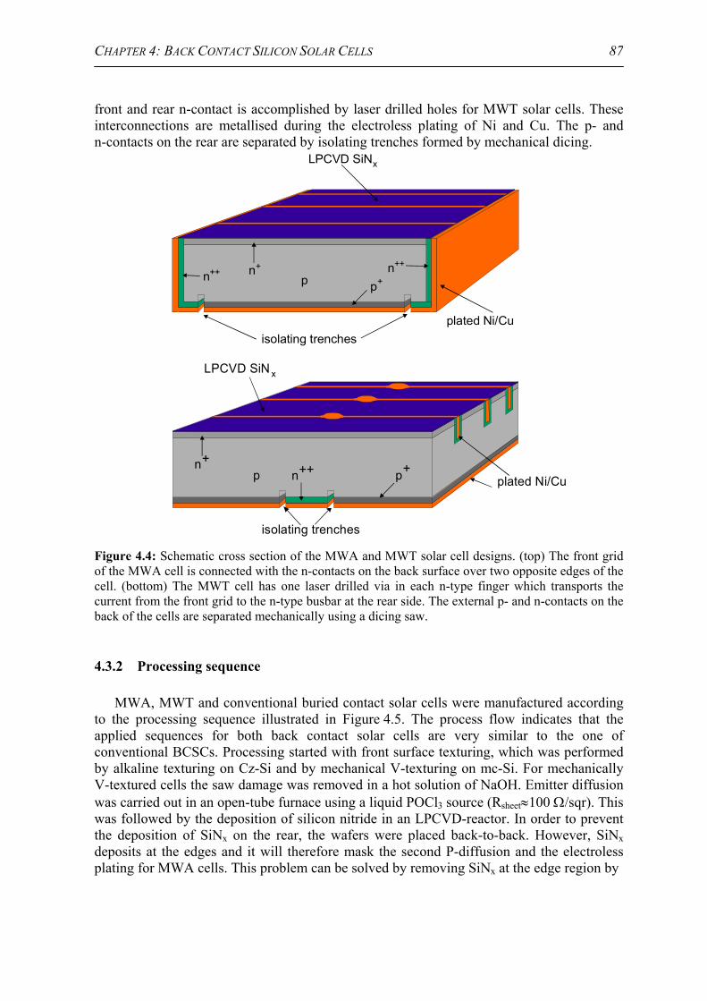
CHAPTER 4: BACK CONTACT SILICON SOLAR CELLS 87
front and rear n-contact is accomplished by laser drilled holes for MWT solar cells. These interconnections are metallised during the electroless plating of Ni and Cu. The p- and n-contacts on the rear are separated by isolating trenches formed by mechanical dicing.
isolating trenchesplated Ni/Cu
pn+
n+++
n++
p
LPCVD SiNx
isolating trenches
n+n++ p+
plated Ni/Cu
LPCVD SiN x
p
Figure 4.4: Schematic cross section of the MWA and MWT solar cell designs. (top) The front grid of the MWA cell is connected with the n-contacts on the back surface over two opposite edges of the cell. (bottom) The MWT cell has one laser drilled via in each n-type finger which transports the current from the front grid to the n-type busbar at the rear side. The external p- and n-contacts on the back of the cells are separated mechanically using a dicing saw.
4.3.2 Processing sequence
MWA, MWT and conventional buried contact solar cells were manufactured according to the processing sequence illustrated in Figure 4.5. The process flow indicates that the applied sequences for both back contact solar cells are very similar to the one of conventional BCSCs. Processing started with front surface texturing, which was performed by alkaline texturing on Cz-Si and by mechanical V-texturing on mc-Si. For mechanically V-textured cells the saw damage was removed in a hot solution of NaOH. Emitter diffusion was carried out in an open-tube furnace using a liquid POCl3 source (Rsheet≈100 Ω/sqr). This was followed by the deposition of silicon nitride in an LPCVD-reactor. In order to prevent the deposition of SiNx on the rear, the wafers were placed back-to-back. However, SiNx deposits at the edges and it will therefore mask the second P-diffusion and the electroless plating for MWA cells. This problem can be solved by removing SiNx at the edge region by

CHAPTER 4: BACK CONTACT SILICON SOLAR CELLS 88
edge+contactisolation
laser drilled vias + etch
edge isolation
metallisation by electroless Ni/Cu plating
P-Al co-diffusion950°C, 30 min
Al evaporation2 µm
NaOH defect etch
mechanical contact groove formation
cutting wafer into size 5x5 cm
LPCVD SiN deposition
POCl emitter diffusion
defect etch + alkaline texturing
edge+contactisolation
MWT conventional MWA
2
3
x
Figure 4.5: Processing sequence for Metallisation Wrap Through (MWT), Metallisation Wrap Around (MWA) and conventional solar cells with buried contacts and electroless plating metallisation.
plasma etching or by manufacturing solar cells with a reduced area compared to the initial wafer size. The second approach was used by cutting four 5x5 cm2 pieces from each 12.5x12.5 cm2 wafer.
The vias for MWT solar cells were drilled using a Nd:YAG system. Hole drilling was done from the rear at a distance of 1.5 mm corresponding to the finger spacing. The vias have a conical shape with a diameter of about 80-90 µm at the entrance (rear) and about 30 µm at the exit (front). Laser processing leads to a laser induced damage which was removed in a hot solution of NaOH at 80 °C for about 4 to 5 min removing 6 to 8 µm of silicon material.
Processing continued with the formation of the contact grooves by mechanical abrasion (finger spacing 1.5 mm). For the MWT solar cells the contact grooves were aligned to the laser drilled vias. The busbars consisted of several fingers and were located on the front for conventional cells and on the rear for MWA and MWT solar cells. The formation of contact fingers for the busbars is in principle not necessary for MWA/MWT solar cells, but it improves the adhesion of the metallisation. The saw damage in the contact grooves was

CHAPTER 4: BACK CONTACT SILICON SOLAR CELLS 89
again removed in NaOH (80° C, 4 min, 6-8 µm). During this etching step, further Si is removed within the vias. After saw damage removal, the diameter of the hole at the rear surface was about 100 µm, on the front 40-50 µm. In principle it should be possible to apply only one defect etch after lasering and contact groove formation. In this experiment the intention was to ensure that the laser damage was completely removed.
The processing sequence also uses P-Al co-diffusion. For MWA/MWT solar cells, the areas designated for the emitter contact were covered by shadowing masks (Si wafers with a width of 2 mm) during the vacuum deposition of 2 µm of Al. Co-diffusion was carried out at 950 °C for 30 min (Rsh≈10 Ω/sq). The cells were metallised by electroless deposition of Ni and Cu. Due to the selective character of this technique, the front grid and rear contact as well as the edges and holes get metallised. In the sequence of MWA/MWT solar cells, the p- and n-contacts on the rear have to be electrically isolated. This was accomplished by an isolating trench (width of dicing blade: 80 µm, depth of the trench: 20 µm). Edge isolation was carried out by mechanical abrasion removing 1 mm from the wafer edges. The final cell area was 23 cm2 for MWT and conventional BCSCs, and 24 cm2 for MWA solar cells on medium cell area. Hence, an additional advantage of MWA solar cells is the larger cell area after edge isolation since a reduced amount of Si has to be removed during edge isolation. In order to reduce the series resistance, the busbars were tabbed with a Cu ribbon 1.5 mm wide and about 120 µm thick.
Results of contact isolation and electroless plating
In the top of Figure 4.6, SEM pictures of specific regions of MWA solar cells after processing are shown. In the left picture, the rear side view of the n-type busbar region with ten contact fingers is visible. In the right part of the picture, the isolating trench can be seen. The right picture shows the plated edge with an incompletely filled buried contact finger in an intermediate stage of plating.
At the bottom of Figure 4.6, SEM pictures of characteristic regions of MWT solar cells are illustrated after electroless plating. The left picture shows the busbar region on the rear of the solar cell with the two isolating trenches. The picture on the right demonstrates that there was sufficient plating inside the via without any unplated areas. The via is not completely filled but the cross sectional area of the plated metal within the via is larger than the cross sectional area of the contact finger leading to an excellent conduction between front side finger grid and rear side busbar.

CHAPTER 4: BACK CONTACT SILICON SOLAR CELLS 90
Figure 4.6: (top) SEM pictures of MWA solar cells, (left) rear side view of busbar region. The isolating trench is visible in the upper right part, ten contact fingers of the busbar in the left part, (right) metallised edge with an incompletley filled groove in an intermediate stage of plating. (bottom) SEM pictures of the contact regions of MWT solar cells. (left) region of the n-type busbar at the rear, which is connected to the front grid on the front by laser drilled vias. In the left and right part the two trenches for p/n contact isolation are visible which were cut by mechanical abrasion. (right) cross section of a plated via. The via has a conical shape, with a diameter of about 100 µm at the entrance side of the laser beam (rear of solar cell) and 40-50 µm at the exit (front of solar cell). In the top region, the intercepting contact groove is visible. The thickness of the Cu layer within the via is about the same as within the grooves. This enables an excellent electrical interconnection between the front grid and the rear side busbar.
IV-measurements
The solar cells were characterised by their illuminated and dark IV-characteristics as well as Jsc-Voc curves. The illuminated IV-parameters for the best cells of the different device designs and crystalline silicon materials are given in Table 4-1. From the same cells the parameters of the Two-Diode model were determined which are given in Table 4-2.

CHAPTER 4: BACK CONTACT SILICON SOLAR CELLS 91
Table 4-1: Illuminated IV-parameters for MWA, MWT and conventional BCSCs for mc-Si and Cz-Si.
cell type Material cell area [cm2]
Voc [mV]
Jsc [mA/cm2]
FF [%]
η [%]
MWA Cz-Si 24 611 37.2 77.2 17.5 MWT Cz-Si 23 612 37.2 75.8 17.2 Conv. Cz-Si 23 612 36.2 76.2 16.9 MWA mc-Si 24 598 35.1 74.9 15.7 Conv. mc-Si 23 599 34.1 76.0 15.5 MWA Cz-Si 98 614 35.9 75.5 16.6
Table 4-2: Parameters of the Two-Diode model extracted from the dark, illuminated and Jsc-Voc characteristics for MWA, MWT and conventional BCSCs.
cell type Material cell area [cm2]
J01 [pA/cm2]
J02 [nA/cm2]
Rsh [Ωcm2]
Rs [Ωcm2]
MWA Cz-Si 24 1.4 45 9000 0.63 MWT Cz-Si 23 1.25 63 1630 0.6 Conv. Cz-Si 23 1.3 44 1200 0.7 MWA mc-Si 24 1.9 120 14000 0.59 Conv. mc-Si 23 1.9 91 16000 0.42 MWA Cz-Si 98 1.0 80 5800 0.53
Discussion Medium cell area
The best MWA solar cell on Cz-Si reached an efficiency of η=17.5%, the best MWT cell of η=17.2% and the conventional one of η=16.9%. Concerning the simplicity of the applied processing sequence, both back contact designs led to very good efficiency and are amongst the highest reported for back contact solar cells using low cost technologies. The short circuit current density Jsc was enhanced by 1 mA/cm2 for both back contact designs as expected due to the reduced shadowing losses of the front metallisation. All cell types obtained almost identical open circuit voltages Voc which is especially encouraging since often a reduced Voc is observed for back contact solar cells (see EWT solar cells in the next section).
The series resistance of all cell types is almost identical which will be expected, if the electrical connection from the front fingers to the rear side busbar is well established. The other main contributions to the series resistance are the same (Remitter, Rfinger, Rcontact and Rbusbar). Therefore an identical series resistance further proofs that the edges and holes are reliably metallised. The shunt resistance for the MWA/MWT cells also shows that contact isolation by mechanical abrasion leads to satisfying results.
The saturation current density of the second diode J02 has contributions from the space charge region and from the “open” p/n junctions J02,surf caused by contact and edge isolation. The last contribution depends on the contact length and is given by [Küh00], [Glu02]:

CHAPTER 4: BACK CONTACT SILICON SOLAR CELLS 92
A
LcmnA13J surf
surf,02 ⋅= (4.2)
Lsurf is the length of the “open” p/n-junctions and A the cell area. The factor of 1.3x10⁻⁸ A/cm is valid if the junction is in a highly damaged region as it is the case after contact and edge isolation applying mechanical abrasion. According to equation 4.2, J02,surf is 1x10⁻⁸ A/cm2 for MWA cells and 1.6x10⁻⁸ A/cm2 for MWT cells. The higher J02 for the MWT solar cell can therefore be attributed to the larger length of “open” p/n-junctions
The results of MWA and conventional solar cells on Baysix mc-Si are also given in Table 4-1 and Table 4-2. Alkaline texturing was replaced by mechanical V-texturing and additionally MIR hydrogen passivation was included (450 °C, 120 min) after P-Al co-diffusion. In principle, the same results were obtained as on Cz-Si with a higher Jsc due to reduced shadowing losses. However, the fill factor was lower for the MWA solar cell due to an enhanced J02 and Rs which can be explained by process variations.
Large area MWA solar cells
For a successful industrial realisation of a new cell design it is necessary that it can be applied on large substrate sizes. MWA solar cells were processed according to the sequence given in Figure 4.5 with a final cell area of 98 cm2. The finger spacing was chosen to 1.0 mm (optimum finger spacing for this cell area for a line resistance of the contact fingers in the range of 400 to 600 mΩ/cm). The illuminated IV-parameters of the best solar cell in this experiment are given in Table 4-1, whereas the parameters of the Two-Diode model are given in Table 4-2. For the best MWA solar cell an efficiency of 16.6% was obtained which is a very promising result. Only Kerschaver et al. [Ker00] reported a higher efficiency of 17.0% for back contact solar cells on large areas (MWA, screen printed metallisation, cell area 10x10 cm2). A higher efficiency in this work was prevented by the rudimentary rear surface passivation of the thin evaporated Al-BSF (see Chapter 2). The fill factor was not limited by the series resistance but by a very high J02 of 8x10⁻⁸ A/cm2.
The discussion on Jsc as well as on the parameters of the Two-Diode model showed that MWA and MWT back contact cells can be described as conventional BCSCs considering small deviations. First of all, these devices exhibit a higher Jsc due to the reduced shading losses. For the medium solar cell areas discussed in this section, the series resistance Rs is the same for MWA, MWT and conventional solar cells. For larger substrate sizes, the series resistance of the MWA solar cell will be higher, unless a reduced finger spacing is chosen (see next section). A slightly higher J02 for the MWT solar cell is a consequence of the higher length of “open p/n-junctions”. For MWT solar cells the additional contribution to J02 due to the larger length of “open” p/n-junctions has to be considered according to equation 4.2. For larger substrate sizes exceeding 100 cm2 the additional contribution is below 0.5x10⁻⁸ A/cm2 and can therefore be neglected.
Deviations also occur due to an additional n-type region on the rear. These regions lead to an increase in Jsc and in J01 as well as J02 (see section on EWT solar cells). However, in MWA/MWT solar cells, these regions cover only a very small fraction of the complete rear surface and the effects on Jsc, J01 and J02 can be neglected. Any additional resistive losses due to current transport to the rear side busbar are of minor importance for the MWT/MWA solar cells of this work.
Therefore in the following simulations, back contact solar cells are described as conventional cells with deviations only concerning resistive as well as shadowing losses.

CHAPTER 4: BACK CONTACT SILICON SOLAR CELLS 93
4.3.3 Grid optimisation for MWA solar cells
The results of the previous section showed, that MWA solar cells lead to higher efficiencies as conventional solar cells on medium substrate sizes. Increasing the cell area for MWA solar cells, or more accurately the width of the solar cell, increases the current path in the contact fingers (which is half of the width using two opposite edges) to the rear side busbar. This increases the contribution of the contact fingers Rfinger to Rs leading to a reduction in fill factor.
The series resistance of the contact fingers Rfinger is given by:
Lld3
RNAl
3RR finger
line
finger
celllinefinger == (4.3)
Rline is the line resistance of the contact finger, Acell the cell area, Nfinger the number of contact fingers, l the current path length in the fingers to the busbar, L the edge length and dfinger the finger spacing.
In order to maintain a high fill factor for MWA solar cells, the finger spacing has to be reduced or the finger conductivity improved. An improved finger conductivity can be achieved by cutting deeper or wider grooves and will be discussed in the next section. A reduced finger spacing inversely affects the efficiency by an enhanced shadowing loss, but was first considered for grid optimisation.
The calculations for grid optimisation were carried out according to the Two-Diode model introduced in Chapter 1. The input parameters J01=1.4x10⁻¹² A/cm2, J02=7x10⁻⁸ A/cm2, Rsh=10000 Ωcm2 and Jsc=34 mA/cm2 (corresponds to 35.8 mA/cm2 when neglecting the shadowing losses of the front metallisation) were taken from experimental data of conventional large area mc-Si solar cells processed with medium cell efficiency in this work. The input parameters determine the overall efficiency but do not influence the general results concerning the optimum grid design as well as the comparison between MWA and conventional solar cells. The series resistance Rs was calculated considering four contributions: emitter (Rsh=100 Ω/sqr), tabbed busbar (line resistance Rbus=0.8 mΩ/cm), contact resistance in the front grid (Rcont=4 mΩcm2) and contact finger.
Rbusbar depends on the measurement set-up, i.e. at which points the busbars are contacted during IV-measurement or during module operation. Generally, large area solar cells are contacted in our institute by two probes per busbar. This leads to an almost negligible contribution of the busbar to the total series resistance. However, the situation is different when the solar cells are interconnected in a module. This corresponds to a measurement setup with one probe at the end of the busbar. This nearly quadruples the contribution of the busbars to the series resistance (often referred to as I2R power loss). Therefore these two cases were calculated for conventional solar cells. In MWA solar cells this loss can be avoided if an optimised backsheet with low resistivity conductors is used for cell interconnection.
Since the series resistance of the contact finger is an important factor for MWA solar cells, the simulations were performed by varying the line resistance between 200 and 600 mΩ/cm. Normally plated buried contact fingers lead to a line resistance of 500 mΩ/cm, whereas lower values can be obtained by cutting deeper contact grooves. The model calculations also consider the shadowing losses of the front grid: for the finger a width of 30 µm was taken, for the busbars a width of 1.5 mm. With these data, the illuminated

CHAPTER 4: BACK CONTACT SILICON SOLAR CELLS 94
IV-curve was calculated and the solar cell parameters were extracted. The calculations were done using a computer programme written by Huster [Hus99].
Results
The results of the calculations for different line resistances of the finger metallisation are summarised in the graphs in Figure 4.7 for a cell area of 10x10 cm2 and 12.5x12.5 cm2. The calculated efficiency is given for MWA as well as for conventional cells with and without I2R power loss of the busbar as a function of line resistance. For each line resistance, the efficiency is a function of finger spacing [Joo00b]. The highest efficiency was taken and plotted in Figure 4.7. For a cell area of 10x10 cm2, the MWA solar cells lead to higher cell efficiencies independently of the line resistance. The additional I2R power loss due to cell interconnection for conventional cells reduces the efficiency η and moves the data points towards lower efficiencies. The slope of the curve for MWA cells is higher compared to conventional cells which follows from the higher contribution of Rfinger to Rs. The optimum finger spacing reduces from 1.2 mm (1.4 mm) at Rline=200 mΩ/cm to 0.9 mm (1.3 mm) at Rline=600 mΩ/cm for MWA (conventional) solar cells.
200 300 400 500 60015.6
15.7
15.8
15.9
16.0
16.1
16.2
16.3
16.410x10 cm2
MWA conv. cell
conv. cell + I2R loss of busbar
η [%
]
line resistance [mΩ/cm]
200 300 400 500 60015.6
15.7
15.8
15.9
16.0
16.1
16.2
16.3
16.412.5x12.5 cm2
MWA conv. cell
conv. cell + I2R loss of busbar
η [%
]
line resistance [mΩ/cm] Figure 4.7: Calculated efficiencies of conventional and MWA solar cells for a cell area of 10x10 cm2 and 12.5x12.5 cm2 as a function of the line resistance of the grid fingers. For the conventional cells the efficiency was also calculated with the I2R power loss of the module interconnection.
The results of the model calculation for a cell area of 12.5x12.5 cm2 are also given in
Figure 4.7. In this case, only for highly conducting fingers the MWA solar cell is still superior to the conventional one without I2R loss. If the I2R power loss is included, the MWA cells obtain higher efficiencies independent of the line resistance. Again the optimum finger spacing reduces from 1.1 mm (1.4 mm) at Rline=200 mΩ/cm to 0.8 mm (1.2 mm) at Rline=600 mΩ/cm for MWA (conventional) solar cells.
The previous calculations were done for a finger width of 30 µm. However, better finger conductivities can also be obtained by cutting wider contact grooves. Additional simulations were carried out for a finger width of 60 µm compared to 30 µm of the previous simulations. In this case, the line resistance will be reduced by a factor of two assuming a complete filling of the grooves, but also the shadowing losses will be enhanced. These simulations showed that the optimum finger spacing will be higher, but the efficiency will be reduced by about 0.25 to 0.3%abs. for a cell area of 10x10 cm2 and by 0.05 to 0.1%abs.

CHAPTER 4: BACK CONTACT SILICON SOLAR CELLS 95
for a cell area of 12.5x12.5 cm2. An additional negative effect for wider contact grooves occur, since the plating time has to be increased to obtain completely filled grooves.
4.3.4 Comparison of MWA/MWT solar cells with conventional BCSCs for different substrate sizes
The experimental results in the previous section indicated that MWA/MWT solar cells can be considered as conventional BCSCs with deviations in resistive as well as shadowing losses. In this section, calculations are carried out by the definition of a “normalised” efficiency which considers only these two deviations. The normalised efficiency ηn is given by
)RR1()M1(
char
s
sRshadn −⋅−=⋅= ηηη (4.4)
ηshad is due to the shadowing losses of the front metallisation and M is the metallised fraction of the front surface. ηRs determines the reduction in fill factor due to the series resistance. The influence of Rs on the fill factor is given by [Gre82]:
)RR1(FFFF
char
s0 −= (4.5)
Rchar is given by Voc/Jsc, which does not significantly depend on the actual solar cell parameter and a value of 17.6 Ωcm2 was taken. The normalised efficiency will be equal to one for negligible shading (M=0) as well as resistive (Rs=0) losses.
As parameters for the calculations, a line resistance of the finger metallisation of 500 mΩ/cm and a groove width of 30 µm were taken which are standard values of conventional BCSCs. For the calculations of the series resistance contributions of the emitter, busbar and the finger metallisation were considered. For the busbars of the conventional cells, a standard thickness for the Cu ribbons of 125 µm was taken [Rob00b], whereas the width was 1.5 mm (2.0mm, 2.5 mm) for 10x10 cm2 (12.5x12.5 cm2, 15x15 cm2) solar cells. Thicker ribbons are difficult to use, since the stress on the wafer edges causes fracture problems during module fabrication. For the back contact solar cells it was assumed that the interconnection on the rear side leads to negligible resistive losses since thicker ribbons or adapted interconnection schemes can be used. For the conventional and MWT cells two busbars were considered independent of the wafer size. For each device design and cell area, the optimum finger spacing was determined and Remitter, Rfinger and the shadowing losses M were calculated. For MWA solar cells a design with wrap around contacts at all four wafer edges was assumed leading to no area losses due to edge isolation. These cells have to be cut into two halves for cell interconnection (see section 5). For MWT and conventional solar cells 1 mm is removed during edge isolation and cleaving [Brut94] which is also included in the calculations. The results of the calculations are illustrated in Figure 4.8.

CHAPTER 4: BACK CONTACT SILICON SOLAR CELLS 96
10.0 12.5 15.00.90
0.91
0.92
0.93
0.94
0.95
0.96three busbars
two busbars
conventional MWA MWT
norm
alis
ed e
ffici
ency
ηn
cell size [cm]
Figure 4.8: Calculated normalised efficiency for different cell sizes of conventional, MWA and MWT solar cells.
The calculations demonstrate that the back contact devices are superior to conventional solar cells independent of the investigated substrate sizes. For a cell area of 10x10 cm2, the MWA and MWT solar cell design lead to a comparable performance. For larger cell areas the MWT cells reaches the highest normalised efficiency. For conventional and MWA solar cells, the efficiency decreases substantially with increasing substrate sizes, whereas the influence of an increase in solar cell area is only minor for MWT solar cells. For MWT cells with a cell area of 15x15 cm2, an increase in efficiency can be achieved by an additional busbar. The calculations demonstrate that the gain in efficiency for the best scenario will be between 4 and 5% compared to conventional BCSCs.
In this section it was demonstrated, that MWA and MWT solar cells lead to higher efficiencies as conventional solar cells. The choice for industrial production will mainly depend on the technique applied for contact groove formation. If contact grooves are formed by mechanical abrasion, the MWA solar cell design is favourable, since it can be fabricated without laser processing. Applying laser ablation for contact groove formation, the holes for MWT solar cells can be formed during groove formation by stopping the laser beam. Also the interconnection of MWA cells seems easier (see section 5), which might favour this design for industrial manufacturing.

CHAPTER 4: BACK CONTACT SILICON SOLAR CELLS 97
4.4 Emitter Wrap Through Solar Cells
In the first section the solar cell design of Buried Contact EWT solar cells is described as it was investigated in this work. The second section deals with the manufacturing of EWT solar cells and two types of conventional cells which were processed for comparison. A detailed analysis of the three device designs investigates the differences and leads to a further understanding of EWT cells. The work on BC-EWT solar cells was motivated by the development of a device design without metallisation on the front surface which is important for some applications of photovoltaic requiring a very high optical appearance. Additionally this design leads to high currents for crystalline silicon materials with a low ratio of bulk diffusion length to cell thickness.
4.4.1 Solar cell description
The principle device design of EWT solar cells was illustrated in Figure 4.2. The current collected in the front side emitter is conducted through laser drilled, diffused and metallised vias to the rear side emitter contact. The rear surface consists of an interdigitated pattern of p- and n-contacts. The specific device design of this work (see Figure 4.9) includes a selective emitter structure. The front surface is coated with LPCVD SiNx for front surface passivation and ARC. Also the rear side is covered by LPCVD SiNx which is opened locally for the n- and p-type contacts. An Al-BSF is formed within the p-type grooves for surface passivation. An emitter is diffused within the n-type contact grooves with a coverage of about 20%. This additional p/n-junction on the rear also collects minority charge carriers leading to an increase in Jsc.
plated Ni/Cu
n++n+p+
LPCVD SiN x
p
Laser drilled vias
LPCVD SiN x Figure 4.9: Schematic drawing of an Emitter Wrap Through (EWT) solar cell with buried contact metallisation. The current collected in the front side emitter is conducted through diffused and metallised holes to the n-type contact finger on the rear. Front and rear surface are coated with LPCVD SiNx, which is locally opened by laser ablation for the p- and n-contacts at the rear surface.

CHAPTER 4: BACK CONTACT SILICON SOLAR CELLS 98
4.4.2 Process technologies and cell layout
As pointed out in section 2, the key task to be solved in the processing of EWT solar cells is the definition of an interdigitated contact pattern with rectifying properties and low contributions to J02 from the “open” p/n-junctions. From the described technologies a diffusion barrier of LPCVD SiNx was selected since it can be easily incorporated in the processing sequence and leads to passivated “open” p/n-junctions with SB in the range of several thousand cm/s. Concerning other process technologies, the aim was to use only techniques, which are currently used in the industrial production of conventional BCSCs including laser processing and vacuum deposition of Al [Mas91].
The previously described MWA and MWT solar cells evolved from the device structure of conventional solar cells. Hence, the basic cell design concerning emitter sheet resistance and finger spacing remained unchanged (except for a reduced finger spacing for large area MWA solar cells). The situation for EWT solar cells is different concerning current flow in the emitter as well as the finger grid and requires considerations concerning the optimum device geometry. In principle, a trade-off has to be made between low resistive losses, mainly in the emitter, and alignment accuracy during subsequent process steps. The interdigitated contact pattern of p- and n-type regions on the rear requires the definition of a large number of rectifying p/n junctions. The distance between fingers of the same polarity influences the series resistance Rs, especially the series resistance in the emitter. Remitter is due to the conduction of the collected carriers in the emitter towards the holes. The conduction through the holes can be neglected, since they are reliably metallised. The Unit Cell (UC) which has to be considered for the calculation of Remitter is shown in Figure 4.10 and is a rectangle with one edge length corresponding to the finger spacing sfinger and the other edge length to the distance between the holes within one contact finger shole. An estimation of Remitter can be made by replacing the rectangular UC by a circular one with the same area (see Figure 4.10). In this case, a simple expression can be derived due to a one-dimensional carrier flow and is given by [Gee93]:
]rln)r1()r1(25.0[2
ARR c2
c4
c
2ucsheet
emitter −−−−=π
(4.6)
Rsheet is the emitter sheet resistance, Auc the area of the unit cell, and rc the diameter of the via divided by the diameter of the circular unit cell. For a low Remitter, the fingers have to be closely spaced, the distance between the holes has to be rather small and the hole diameter has to be large. A lower value of the emitter sheet resistance Rsheet also reduces Remitter, but inversely affects the IQE in the short wavelength range.
On the other side, the fingers of the interdigitated contact pattern have to be reliably defined and metallised. This is facilitated by a rather wide finger spacing allowing contact alignment of the shadowing masks before the vacuum deposition of Al in the p-type grooves. The chosen trade-off was a distance of 2 mm between fingers of the same polarity. Another trade-off is between processing time and series resistance. The distance between the holes in one finger was chosen rather large (800 µm) in order to reduce the processing time for hole formation. The diameter of the holes after etching was about 120 µm at the entrance side of the laser beam (rear) and about 80 µm at the exit. Remitter will be lower if lasering of the holes is done from the front surface. However, this requires an additional alignment step of the holes to the n-type grooves which was not considered in this work in order to maintain a simpler processing sequence. Figure 4.11 shows the rear side of an

CHAPTER 4: BACK CONTACT SILICON SOLAR CELLS 99
EWT solar cell after lasering and laser damage removal. A SEM picture of a laser drilled via is also given in Figure 4.11.
rectangular unit cell
circularunit cell
D
DSfinger
uc
hole
Shole
laser drilledvias
Figure 4.10: Unit cell (UC) for the calculation of the series resistance in the emitter of EWT solar cells. For an estimation of Remitter in EWT solar cells, the rectangular UC was replaced by a circular one with the same area. A simple expression can be derived due to one-dimensional current flow (see text). sfinger is the finger spacing, Dhole is the diameter of the hole and Duc the diameter of the circular UC.
Figure 4.11: SEM pictures of characteristic regions of BC-EWT solar cells, (left) laser grooved contacts after alkaline defect etch, the left groove corresponds to the p-contact, the right groove with laser drilled vias to the n-contact, (right) laser drilled via. The via has a conical shape with a larger diameter at the entrance side of the laser beam (rear).
4.4.3 Processing sequence
The applied processing sequence for EWT solar cells is given in Figure 4.12. Additionally two types of conventional solar cells were processed for comparison. The first one is a conventional solar cell with a full area Al-BSF whereas for the second one the rear side is passivated by LPCVD SiNx and locally opened for the rear contact. The processing sequences for both types of reference cells are also given in Figure 4.12. Equal material quality was ensured by processing all three types on a single large area wafer.

CHAPTER 4: BACK CONTACT SILICON SOLAR CELLS 100
POCl emitter diffusion80 Ω/sqr
lasering of holes and grooves
edge isolation
electroless metal deposition
P-Al co-diffusion
Al deposition
alkaline defect etch
grooves on front and rear
cutting wafer in 5 cm x 5 cm
LPCVD SiN on rear
emitter removal on rear by wet chemical etching
LPCVD SiN deposition on front
POCl emitter diffusion
defect etch and alkaline texturing
grooves on front+SiN removal
EWT conventional(local rear contact)
conventional(full rear contact)
X
X
X
edge isolation
metallisation by electroless Ni/Cu plating
P-Al co-diffusion950°C, 30 min
Al evaporation2 µm
NaOH defect etch
3
Figure 4.12: Processing sequences for Emitter Wrap Through (EWT) solar cells and two types of conventional BCSCs. (left) Emitter Wrap Through, (middle) conventional with local rear contact (right) conventional with full area rear contact. The process for the conventional solar cell with full rear contact was modified for this investigation in order to do as many process steps in parallel for all three devices. Therefore for conventional BCSCs with full rear contact, LPCVD SiNx was deposited on the rear and removed by mechanical abrasion using dicing blades.
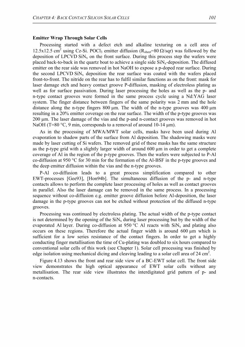
CHAPTER 4: BACK CONTACT SILICON SOLAR CELLS 101
Emitter Wrap Through Solar Cells Processing started with a defect etch and alkaline texturing on a cell area of
12.5x12.5 cm2 using Cz-Si. POCl3 emitter diffusion (Rsheet=80 Ω/sqr) was followed by the deposition of LPCVD SiNx on the front surface. During this process step the wafers were placed back-to-back in the quartz boat to achieve a single side SiNx-deposition. The diffused emitter on the rear side was removed in hot NaOH to expose a p-doped rear surface. During the second LPCVD SiNx deposition the rear surface was coated with the wafers placed front-to-front. The nitride on the rear has to fulfil similar functions as on the front: mask for laser damage etch and heavy contact groove P-diffusion, masking of electroless plating as well as for surface passivation. During laser processing the holes as well as the p- and n-type contact grooves were formed in the same process cycle using a Nd:YAG laser system. The finger distance between fingers of the same polarity was 2 mm and the hole distance along the n-type fingers 800 µm. The width of the n-type grooves was 400 µm resulting in a 20% emitter coverage on the rear surface. The width of the p-type grooves was 200 µm. The laser damage of the vias and the p-and n-contact grooves was removed in hot NaOH (T=80 °C, 9 min, corresponds to a removal of around 10-14 µm).
As in the processing of MWA/MWT solar cells, masks have been used during Al evaporation to shadow parts of the surface from Al deposition. The shadowing masks were made by laser cutting of Si wafers. The removed grid of these masks has the same structure as the p-type grid with a slightly larger width of around 600 µm in order to get a complete coverage of Al in the region of the p-type grooves. Then the wafers were subjected to P-Al co-diffusion at 950 °C for 30 min for the formation of the Al-BSF in the p-type grooves and the deep emitter diffusion within the vias and the n-type grooves.
P-Al co-diffusion leads to a great process simplification compared to other EWT-processes [Gee93], [Hon94b]. The simultaneous diffusion of the p- and n-type contacts allows to perform the complete laser processing of holes as well as contact grooves in parallel. Also the laser damage can be removed in the same process. In a processing sequence without co-diffusion e.g. emitter groove diffusion before Al-deposition, the laser damage in the p-type grooves can not be etched without protection of the diffused n-type grooves.
Processing was continued by electroless plating. The actual width of the p-type contact is not determined by the opening of the SiNx during laser processing but by the width of the evaporated Al layer. During co-diffusion at 950 °C Al reacts with SiNx and plating also occurs on these regions. Therefore the actual finger width is around 600 µm which is sufficient for a low series resistance of the contact fingers. In order to get a highly conducting finger metallisation the time of Cu-plating was doubled to six hours compared to conventional solar cells of this work (see Chapter 1). Solar cell processing was finished by edge isolation using mechanical dicing and cleaving leading to a solar cell area of 24 cm2.
Figure 4.13 shows the front and rear side view of a BC-EWT solar cell. The front side view demonstrates the high optical appearance of EWT solar cells without any metallisation. The rear side view illustrates the interdigitated grid pattern of p- and n-contacts.

CHAPTER 4: BACK CONTACT SILICON SOLAR CELLS 102
Figure 4.13: (left) front side view of a BC-EWT solar cell. The laser drilled holes are visible in a horizontal structure. (right) rear side view with the interdigitated pattern of p-and n-contacts. The p-type busbar is located at the left side.
Conventional BCSC with full area back surface field
The solar cells were processed on the same wafer with the EWT solar cells up to the second LPCVD-SiNx deposition (wafer size of 12.5x12.5 cm2). The SiNx was removed on the rear surface by mechanical abrasion leading to a slightly reduced cell thickness (about 10 µm). Also the defect etch within the contact grooves (formed by mechanical abrasion) was done in parallel with the other cell designs. In this case a rather large amount of Si was removed (80° C, 9 min) to account for the deeper laser damage in EWT solar cells. This leads to wider contact grooves (45 µm instead of 30 µm) enhancing the shadowing losses.
Conventional BCSC with local back surface field
Processing up to the second SiNx-deposition was identical to EWT solar cells. The p-type grid on the rear was opened locally by laser ablation with the same design as the p-type grid of EWT solar cells. The front grid was formed by mechanical abrasion with a finger spacing of 1.5 mm. Further processing was identical as for the conventional BCSC.
Before solar cell characterisation the busbars of all three cell types were tabbed using 1.5 mm wide Cu ribbons.
IV-measurements
In Table 4-3 the parameters of the illuminated IV-measurements are given for the best solar cells of the three solar cell designs. The EWT solar cell reached an efficiency of η=16.6%. This is to the knowledge of the author the highest efficiency obtained so far on an EWT solar cell using industrial production technologies without photolithography on medium cell areas. The conventional solar cell with full area rear contact reached an efficiency of 16.6%, with local rear contact of 15.7%. The highest short circuit current density Jsc in this investigation was 37.4 mA/cm2 for the EWT cell. However, the enhanced Jsc was balanced by a considerably reduced Voc and fill factor compared to the conventional one with full area rear contact therefore leading to the same η.

CHAPTER 4: BACK CONTACT SILICON SOLAR CELLS 103
Table 4-4 denotes the parameters of the Two-Diode model of the three cell designs. The difference in Voc of 21 mV between the EWT cell and the conventional BCSC with full rear contact is caused by an increase in J01 from 1.3x10⁻¹² A/cm2 to 2.5x10⁻¹² A/cm2 (15 mV) and in J02 from 4.1x10⁻⁸ A/cm2 to 8.9x10⁻⁸ A/cm2 (6 mV). Table 4-3: Illuminated IV-parameters for BC-EWT solar cells and two types of conventional BCSCs on Cz-Si with a cell area of 24 cm2.
Cell type Voc [mV]
Jsc [mA/cm2]
FF [%]
η [%]
EWT 591 37.4 75.1 16.6 Conv. with full area BSF 612 35.2 77.1 16.6
Conv. with local BSF 607 34.2 75.6 15.7
Table 4-4: Parameters of the Two-Diode model extracted from the dark, illuminated and Jsc-Voc characteristics for BC-EWT solar cells and two types of conventional BCSCs.
Cell type J01 [10-12A/cm2]
J02 [10-8A/cm2]
Rsh [Ωcm2]
Rs [Ωcm2]
EWT 2.5 8.9 1600 0.72 Conv. with full area BSF 1.3 4.1 1900 0.62
Conv. with local BSF 1.5 4.3 1200 0.84 The previous short discussion of the IV-characteristics gives only a very basic
understanding of the BC-EWT cells in comparison to the conventional ones. Further cell characterisation in the next sections will answer the following questions leading to a quantitative explanation: • How large is the current gain due to the second carrier collection on the rear surface? • What is the reason for the reduced Voc mainly caused by a significantly higher J01? • What is limiting the fill factor of the EWT cell?
4.4.4 Optical and electrical analysis
The increase in Jsc for the EWT cell compared to the cell with full area BSF was 2.2 mA/cm2 (6.3% rel.), to the one with local BSF 3.2 mA/cm2 (9.4% rel.). This is caused by two effects:
1. A negligible shadowing loss of the front grid 2. An additional carrier collection at the p/n-junction at the rear surface A detailed analysis of the current gain requires the measurements of the reflectivity as
well as local LBIC-mappings, which will be presented in the first part. The analysis of the two contributions to the current gain is carried out after these characterisations.

CHAPTER 4: BACK CONTACT SILICON SOLAR CELLS 104
400 500 600 700 800 900 1000 11000
20
40
60
80
100
EWT local BSF full BSFE
QE
[%],
refl
[%]
λ [nm]
Figure 4.14: External Quantum Efficiency (EQE) and reflectivity of a BC-EWT cell and two designs of conventional BCSCs.
4.4.4.1 Spectral response and reflectivity measurements
The results of the measurements (EQE and reflectivity) on an illuminated cell area of 2x2 cm2 are shown in Figure 4.14. The reduced shadowing losses of the EWT solar cell can be seen in the reflection curves. All three cell types have the same EQE in the short wavelength range up to about 800 nm. In this range the EQE is slightly lower than for other BCSCs processed in this work due to recombination in the higher doped emitter (Rsheet=80 Ω/sqr instead of 100 Ω/sqr). The highest EQE for wavelengths larger than 900 nm is obtained for the EWT solar cell mainly caused by double sided collection of the minority charge carriers.
A spectral analysis of the IQE was carried out to extract the effective bulk diffusion length (see Chapter 1). The effective bulk diffusion length is Leff=240 µm for the BCSC with full area rear contact and Leff=210 µm for the locally contacted one. The spectral analysis in this form can not be used for EWT solar cells, since the deviation of the spectral analysis is not valid for double sided collection. The reason for the difference in Leff for the two conventional BCSCs will be analysed by LBIC scans in the next section.
4.4.4.2 LBIC measurements
A spatially resolved characterisation of the three cell designs was carried out by SR-LBIC [Per02] and is illustrated as Leff-mappings in Figure 4.15. For the EWT solar cell, the analysis for the determination of Leff is not valid in the n-type regions on the rear. The black box in each mapping indicates the area, where the spectral response and reflectivity measurements of the previous section were carried out.

CHAPTER 4: BACK CONTACT SILICON SOLAR CELLS 105
Figure 4.15: Mappings of the effective diffusion length Leff obtained by SR-LBIC. (top) EWT solar cell, (middle) conventional BCSC with full area rear contact ,(bottom) conventional BCSC with local rear contact. The black box indicates the regions where the spectral response and reflectivity measurements of the previous section were carried out.

CHAPTER 4: BACK CONTACT SILICON SOLAR CELLS 106
The spatially resolved LBIC scan of the EWT solar cell clearly shows the increased current collection underneath the n-type finger contacts on the rear which can be seen in the horizontal linear structure. The circular structure originates from local variations in the bulk lifetime caused by a non-optimised thermal cycle during high temperature processing. Cz-Si should be processed with fast temperature ramps (e.g. loading and unloading at high temperatures), whereas mc-Si and FZ-Si is best processed with slow temperature ramps. The high temperature processes in this work were optimised for mc-Si leading to non-optimum conditions for Cz-Si.
In the Leff-mapping of the conventional cell with full area rear contact, the circular structure is reduced. Only a small region in one corner has a lower Leff.
Two linear structures can be seen in the LBIC scan of the locally contacted conventional cell (see bottom in Figure 4.15). The one in horizontal direction is due to the finger metallisation. The higher current in the vicinity of the buried contact finger is due to the vertical emitter within the contact grooves which leads to an improved current collection. The vertical structure in the LBIC scan is due to the local rear contacting scheme. In the lower right part of the cell corresponding to a high Leff, this vertical structure is not pronounced. This indicates, that the rear surface recombination velocity is similar for the LPCVD SiNx and for the thin evaporated Al-BSF which is in the range of 5000 cm/s. Only in regions with a high diffusion length, the rear surface recombination velocity influences Leff (see Figure 2.19). In the upper left part of the LBIC-mapping the vertical structure due to the local rear contact scheme is very pronounced. In this region, Leff is low and therefore any differences in rear surface recombination are not responsible for local variations in Leff. Local variations in this part are caused by differences in the bulk diffusion length LB. A possible explanation is an Al-gettering effect leading to an increase in LB on the regions covered by Al since regions coated with LPCVD SiNx can not be gettered. A further indication of this effect is the LBIC-mapping of the conventional cell with full rear contact, since a circular structure is almost not visible for this cell. 4.4.4.3 Current gain due to double sided charge carrier collection
The effect of double sided minority charge carrier collection leads to an increase in Jsc and was investigated by several authors including [Ker00b], [Kre01], [Kna01]. Parts of the investigations in [Ker00b] are applied to the EWT solar cells of this work. The left side of Figure 4.16 shows the Collection Probability (CP) for (a) a conventional cell with unpassivated rear contact and for (b) a partly double sided collecting structure [Ker00b]. This figure shows that minority charge carriers generated deeply inside the bulk above the area with two emitters have a higher CP therefore leading to an increase in Jsc.
The right part of Figure 4.16 shows the relative current gain due to the double sided collection for different rear surface recombination velocities SB of the single sided cell for a cell thickness of 280 µm [Ker00b]. In these simulations the rear surface is completely covered with a second collecting junction. The relative difference in Jsc can be as high as 8% if compared to a single sided cell with poor rear surface passivation. If the rear surface passivation of the single sided cell is improved, a current gain up to 5% can be achieved if the bulk diffusion length corresponds to about half of the cell thickness. For the EWT cells in this work, SB for the thin evaporated Al-BSF as well as for the regions passivated by LPCVD SiNx, will be about 5000 cm/s. The diffusion length is varying between 100 and 200 µm (see LBIC scans). For these parameters, the corresponding gain in Jsc is in the range of 5 to 7%.

CHAPTER 4: BACK CONTACT SILICON SOLAR CELLS 107
Figure 4.16: (left) Collection probability (CP) of minority charge carriers for (a) a conventional solar cell with unpassivated rear contact and (b) partly double sided collecting cell for a bulk diffusion length of 100 µm. (right) Simulated current gain of double sided collecting designs compared to conventional designs for a wafer thickness of 280 µm (both from [Ker00b]).
In the investigated design of BC-EWT cells, a second collecting junction is only
underneath the regions opened by laser ablation with a width of 400 µm and amount therefore to about 20% of the area. However, the physical width and the “electrically active width” of the n++-region is not the same, as these regions are “smeared out” (see Figure 4.16). To further quantify this effect, linescans of the IQE at λ=980 nm are given for the EWT cell in Figure 4.17 for regions with high (black) and low (red) effective diffusion lengths. The electrically active width was determined as the width when the IQE reaches half of the value between high IQE (with the second collecting junction) and low IQE (LPCVD SiNx and Al-BSF, p-type regions). For the regions with a high Leff, the width is about 600 µm, for the region with a low Leff it is 750 µm. As an average value 700 µm was taken for the electrical width of the n-type fingers for the analysis performed in the next section since a large fraction of the EWT solar cell has a lower Leff.
2 3 4 5 6 7 8 950
55
60
65
70
75
80
85
90
750 µm
600 µm
IQE
at λ
=980
nm
distance [mm]
Figure 4.17: Linescans of the IQE determined from an LBIC-mapping at λ=980 nm. The black curve corresponds to the region with high Leff in the upper right part of the Leff-mapping in Figure 4.15, the red curve to the region with low Leff in the lower right part. The red curve intercepts the holes leading to dips in the regions of a high IQE.

CHAPTER 4: BACK CONTACT SILICON SOLAR CELLS 108
4.4.4.4 Discussion 1. Current gain due to reduced shadowing losses The non-active cell area for the EWT solar cell due to the holes is below 0.2%. The
contact fingers of the conventional cells were slightly wider (45 µm) as in standard cell processing (30 µm) since the defect etch of the contact grooves was enhanced (see section 4.4.3). The shadowing losses of the contact finger therefore amount to 3%, from the tabbed busbar also to 3%. Therefore the reduced shadowing losses correspond to a difference in Jsc of 2.2 mA/cm2.
2. Current gain due to second collecting junction on the rear The model calculations of [Ker00b], introduced in the previous section, showed, that a
second collecting junction on the complete rear side leads to an increase in Jsc of 5-7%. The electrically active width of the n++-type region on the rear corresponds to 700 µm wheareas the “physical” width was only 400 µm. Therefore the double sided collecting junction on the rear covers 35%. The increase in Jsc will be in the range of 1.8-2.5% corresponding to 0.6-0.85 mA/cm2. In order to determine the experimental increase in Jsc due to rear side current collection, the difference between the EWT cell and the locally contacted conventional BCSC has to be taken, since these cells have a very similar distribution of Leff. The difference in Jsc between these two cells amounted to 3.2 mA/cm2 leading to an increase of 1 mA/cm2 due to current collection in the rear side junction. This is very close to the calculated increase in Jsc and lies within measurement uncertainty.
4.4.5 Enhancement in J01 due to the second carrier collecting junction
J01 is the sum of contributions from the emitter J01e and the base J01b. J01e was experimentally determined on test structures and is around J01e=0.3x10⁻¹² A/cm2 including the effect of surface enlargement due to alkaline texturing (see Chapter 1). The base contribution is proportional to 1/Leff. Therefore a lower Leff will lead to an increase in J01. This effect explains the difference between the conventional cell (J01=1.3x10⁻¹² A/cm2) and the cell with local rear contact (J01=1.5x10⁻¹² A/cm2). However, the significantly higher J01 of the EWT has a different nature and has to be attributed either to the different device design or to differences in the processing (e.g. lasering of the holes leading to a laser damaged region). In the following, the influence of the cell design is investigated by a simple model described in [Ker00b] and also applied in [Kre01] and [Kna01b].
The 1-dim. model explains, that the second junction on the rear leads to an enhanced J01 if LB is not exceeding half of the cell thickness. Under the assumption, that LB is small compared to the cell thickness, the p/n-junctions on front and rear can be considered as two diodes connected in parallel (see Figure 4.18). This assumption is valid for most parts of the EWT cell with LB in the range of 100 µm to 200 µm.

CHAPTER 4: BACK CONTACT SILICON SOLAR CELLS 109
Figure 4.18: Simplified circuit model of a double junction structure (from [Ker00b]).
The IV-characteristics of the two diodes are given by [Ker00b]:
)Tk/qVexp(JJJ Bf,01f,phf −= (4.7)
)Tk/qVexp(JJJ Br,01r,phr −= (4.8)
Jph,f is the photo current collected in the front junction. Under front illumination, Jph,f is higher as Jph,r, the current collected at the rear junction. J01,f and J01,r are the saturation current densities of the front and rear junction. The illuminated IV-characteristics of the cell according to the circuit given in Figure 4.18 are: )Tk/qVexp(JJ)Tk/qVexp()JJ(JJJJJ Btot,01tot,phBr,01f,01r,phf,phrftot −=+−+=+= (4.9)
Therefore, the total dark saturation current density J01,tot increases and is higher as for the conventional single sided cell. Since Jph,tot does not increase with the same factor, this results in a decrease in Voc. This model can not be applied for diffusion lengths exceeding the cell thickness. In this case, carriers injected from the front junction can be collected at the rear junction and vice versa.
The base contribution from the front junction will be about J01b=1.2x10⁻¹² A/cm2 (J01 from the conventional with local rear contact minus J01e). For the EWT cell, also the rear junctions and the area surrounding the holes have to be included. In this case, also the “electrical” area has to be taken, which extends the “physical” area of the junction by about the diffusion length assuming 150 µm for LB. This area corresponds to 8.4 cm2 from the emitter fingers and 2.4 cm2 from the holes. Therefore the contribution due to the additional area will be 0.55x10⁻¹² A/cm2 (corresponding to 45% from the front emitter). Due to the high doping underneath the metal contacts, the contribution to J01e has not to be considered (see Chapter 1). Therefore the sum of all contribution (emitter, base front, base rear) amounts to J01=2.05x10⁻¹² A/cm2 for the EWT design. This value corresponds well to the investigations performed by Kress on screen printed EWT solar cells and test structures [Kre01]. Still a difference of 0.45x10⁻¹² A/cm2 remains between the calculated and measured value which can not be explained by the effects considered up to this point.
One explanation for this difference is a damaged region after laser processing which was not completely removed during the alkaline damage etching step. This explanation is further supported by an increase in J02 since a laser damage will also enhance the generation/recombination currents within the space charge region (see next section).

CHAPTER 4: BACK CONTACT SILICON SOLAR CELLS 110
4.4.6 Fill factor of EWT solar cells
The differences in the fill factor between the conventional and EWT solar cells arise from variations in the series resistance and J02.
For the EWT solar cell, a significantly higher J02 of 8.9x10⁻⁸ A/cm2 was measured compared to 4.1x10⁻⁸ A/cm2 for the conventional BCSCs. This leads to a decrease in Voc of 6 mV and in fill factor of 2%abs. The increase in J02 was most probably caused by an incompletely removed laser damage within the vias and underneath the contacts. A laser damage induced reduction of the solar cell efficiency can either be avoided by longer etching times or by the application of modified laser parameters during hole drilling. Series resistance
The series resistance for the three devices vary between 0.62 and 0.84 Ωcm2. Especially a series resistance of 0.72 Ωcm2 is a very low value for an industrial type EWT solar cell. The different contributions to the series resistance were calculated as described in Chapter 1 and equation 4.6 and are given in Table 4—5 for the three device designs. The following input parameters have been used: emitter sheet resistance Rsheet=80 Ω/sqr, line resistance of the front fingers (both conventional cells) Rline=500 Ω/cm, line resistance for EWT of n-type fingers Rline,n=35 mΩ/cm and p-type fingers Rline,p=30 mΩ/cm. Due to the reduced plating time for the locally contacted BCSC, the p-type fingers have a line resistance of 60 mΩ/cm.
Table 4-5: Contributions to the series resistance Rs in Ωcm2 for the three cell designs.
Cell design Emitter Finger n Finger p Contact Rs Rs,measured EWT 0.44 0.06 0.05 0.03 0.58 0.72
Conventional 0.16 0.16 - 0.06 0.38 0.62 Local 0.16 0.16 0.1 0.06 0.48 0.84 The calculated Rs for the conventional BCSCs is significantly lower as the measured
one. Visual inspection revealed that the adhesion within the contact grooves was moderate. This problem occurred since the contact grooves are rather wide and Ni was not sintered to achieve good adhesion. During Cu-plating the mechanical stress increases and the Ni/Cu metal layer is partly released from the walls. Also the Cu-plating within the grooves was not optimum. Therefore the difference between the measured and calculated series resistance for both conventional BCSCs is most probably due to an enhanced Rcontact as well as Rfinger of the n-finger.
For the EWT solar cells the contribution of the finger grid to Rs is well below 0.2 Ωcm2. This is a consequence of the cell design, since the trade-off between shading and resistive losses is not present for these devices. The major contribution to Rs is from the spreading resistance of the emitter. Remitter for the EWT solar cell was calculated according to equation 4.6 and leads to 0.44 Ωcm2. Remitter has to be reduced to reach a Rs below 0.5 Ωcm2. This can be accomplished by a larger diameter of the vias (increase from 100 µm to 200 µm causes a decrease in Remitter from 0.44 to 0.3 Ωcm2) or by a smaller distance between the holes within one contact finger (reducing from 800 µm to 400 µm leads to a decrease from 0.44 to 0.28 Ωcm2).

CHAPTER 4: BACK CONTACT SILICON SOLAR CELLS 111
Further improvements in solar cell efficiency for EWT solar cells Besides decreasing the laser induced damage in the vias, improvements in the solar cell
efficiency of EWT cells can be achieved by increasing the width of the second collecting junction on the rear. For similar bulk diffusion lengths in the range of 100 to 200 µm, a doubling will lead to an increase in Jsc of about 0.6 to 0.8 mA/cm2 and to a reduction in Voc of about 7 mV. The overall increase in efficiency will be in the range of 1%rel. A reduction of the hole spacing within the n-type finger from 800 µm to 400 µm will decrease the series resistance by 0.16 Ωcm2, leading to an improvement in the fill factor of 0.9%abs. Hence, an efficiency exceeding 17% is possible.
4.5 Interconnection schemes for back contact solar cells
The co-planar arrangement of p- and n-contacts on the rear in back contact solar cells allows a simplified cell interconnection. Gee et al. [Gee97] suggested a scheme for interconnection (see Figure 4.19), which takes the full benefit of back contact solar cells. The basic features are a back contact solar cell, a module backsheet with the electrical circuit as well as the encapsulant in one piece [Gee97]. The main advantage of this encapsulation technique is a significant cost reduction (about 50% of module fabrication resulting in a reduction of complete module costs of 25%), easier automation and the reduction of process steps. In contrast, the module fabrication of standard cells requires tabbing of individual cells, interconnection of the cells between each other, transport of the array to encapsulation and lamination. For the electrical interconnection of back contact cells to the back sheet several techniques are feasible e.g. conductive adhesives [Eic01] and soldering [Gee97]. However, the research on this approach for cell interconnection is not completed yet. Kerschaver et al [Ker02] suggested in an intermediate stage to apply a conventional stringing approach for back contact solar cells.
Figure 4.19: Simplified module manufacturing with back contact solar cells [Gee97].

CHAPTER 4: BACK CONTACT SILICON SOLAR CELLS 112
Interconnection schemes for MWA solar cells A very simple and possibly the most effective way of cell interconnection is achieved
when the initial MWA solar cell with wrap around contacts on opposite cell edges is cut into two halves at the end of the process leading to a device design with only one wrap around contact. This process requires edge isolation at two edges. The cell interconnection for this cell design is shown in the upper part of Figure 4.20. In this case, the current transport in the interconnection on the backsheet is only a few mm compared to the cell length in the interconnection of conventional solar cells. If the cells are not cut into two halves, an interconnection scheme as indicated in the lower part of Figure 4.20 is possible.
A different grid design of MWA solar cells with wrap around contacts at four edges is very attractive. In this case no silicon material has to be removed during edge isolation. The grid design has to be modified in order to transport the current to the four edges and the cells have to be cut into two halves for simplified interconnection. The cell interconnection would be similar to the one shown in the lower part of Figure 4.20.
n-type contact
p-type contactor glass substrate with contactsInterconnection, e.g. copper foil
SiN-ARC
Figure 4.20: Suggestion of two possible interconnection schemes for MWA solar cells.
CHAPTER 4: BACK CONTACT SILICON SOLAR CELLS 113
4.6 Summary
In this Chapter MWA, MWT and EWT back contact solar cells were fabricated and characterised. For each design a processing sequence was developed which is applicable for industrial manufacturing.
Solar cell efficiency For MWT and MWA solar cells, high efficiencies were demonstrated with η=17.5% for
MWA and η=17.2% for MWT solar cells on medium cell areas using Cz-Si. These are the highest efficiencies reported for back contact solar cells applying low cost production technologies. On a cell area of 98 cm2, an efficiency of 16.6% was achieved on MWA solar cells. The gain in η compared to the conventional BCSCs was caused by reduced shadowing losses due to the absence of the front side busbar. An additional gain in electric power can be obtained for MWA solar cells, since no silicon material has to be removed during edge isolation. Model calculations were carried out to investigate the increase in module power for MWA/MWT solar cells compared to conventional BCSCs. It was demonstrated, that for substrate sizes up to 15x15 cm2, the gain in module power will be in the range of 4-5% compared to conventional modules. For a substrate sizes of 10x10 cm2, the MWA and MWT designs lead to a similar performance, whereas for larger sizes, the MWT concept is superior.
For the EWT design, an efficiency of η=16.6% was achieved on a solar cell area of 24 cm2. This is the highest efficiency obtained for EWT solar cells applying industrial production technologies without photolithography. Due to a negligible shadowing loss of the front side, a high Jsc of 37.4 mA/cm2 was obtained. The increase in Jsc was balanced by a reduction in Voc (∆Voc=21 mV) and FF (∆FF=2%abs.) compared to a conventional BCSC. A spectral and electrical analysis revealed that the increase in Jsc compared to a conventional solar cell is 2.2 mA/cm2 due to reduced shading losses and 0.6 to 0.85 mA/cm2 due to the second collecting junction. It was demonstrated that a decrease in Voc is a consequence of the second junction on the rear, if the bulk diffusion length is in the order of half of the cell thickness or below. This effect could only explain a reduction in Voc of 7 mV. A higher efficiency for the EWT solar cell was prevented by an incompletely removed laser damage leading to an enhanced J01 and J02, reducing Voc by 9 mV and FF by 1.8%abs. By solving this problem, efficiencies exceeding 17% are feasible.
Processing sequences and fabrication
Processing of back contact solar cells applying the buried contact technology with electroless plating metallisation has the following advantages:
• High finger conductivity in conjunction with low shadowing losses • Reliable metallisation of interconnections: edges in MWA solar cells and vias in
MWT/EWT solar cells The basic idea behind MWA solar cells is a simple realisation of a back contact solar
cell since laser processing for hole formation can be avoided. The processing sequence is almost identical to conventional solar cells and only additional process steps are necessary for the removal of SiNx at the edges and contact isolation by isolating trenches. Hole formation by laser ablation is necessary in the manufacturing of MWT solar cells. If laser systems are already applied for contact groove formation, the holes can be introduced in

CHAPTER 4: BACK CONTACT SILICON SOLAR CELLS 114
parallel with the grooves. In this case, only additional contact isolation has to be performed by mechanical abrasion.
In the processing of EWT solar cells, laser processing is necessary to form a large number of holes. The definition of the interdigitated contact pattern on the rear was accomplished by a patterned diffusion barrier of LPCVD SiNx. P-Al co-diffusion led to a significant process simplification when compared to other processing sequences for BC-EWT solar cells. This also allows the lasering of the p- and n-type grooves as well as the holes in parallel.

115
Summary This thesis examines multicrystalline silicon (mc-Si) as well as back contact solar cells
applying the Buried Contact Solar Cell (BCSC) technology. In this metallisation approach, the electric contacts are buried into the silicon wafer leading to low shadowing losses in conjunction with highly conducting contact fingers. Further features include a selective emitter structure as well as surface passivation. BCSCs are currently manufactured with the highest efficiencies in industrial solar cell production on monocrystalline Cz-Si, whereas the production of mc-Si solar cells is currently not pursued mainly due to the lack of an adapted processing sequence resulting in sufficient efficiencies.
The fabrication of mc-Si as well as back contact solar cells requires a baseline process for conventional BCSCs which was investigated in the first part. New processing steps compared to present industrial manufacturing include P-Al co-diffusion for the simultaneous groove diffusion and Al-alloying as well as contact groove formation by mechanical dicing instead of laser scribing. The developed electroless plating sequence of Ni and Cu leads to a high quality front surface metallisation with low shadowing losses (about 4-5 %) and good finger conductivities. High fill factors up to 79.8 % and a series resistance Rs below 0.4 Ωcm2 were demonstrated proving the quality of the developed solar cell metallisation.
In order to achieve high efficiencies on multicrystalline silicon, mechanical front surface texturing and bulk passivation have been implemented into two different processes which differ in rear surface passivation. In Process I the rear surface is passivated by a thin evaporated Al-BSF whereas in Process II a thicker BSF layer with improved rear surface passivation was realised by screen printing of Al and firing.
Mechanical V-texturing was examined by single blade texturing as well as wheel texturing. The improvements in Jsc due to the reduction of front surface reflection and due to the enhancement in collection probability of minority charge carriers in the macroscopic V-texture were quantified and verified by the processing of solar cells. An increase in Jsc of 1.5 mA/cm2 and in η of 0.7 %abs. has been demonstrated for wheel textured solar cells.
Multicrystalline silicon has a higher defect density as compared to mono-Si. This is caused by crystallographic defects and by metallic impurities leading to reduced bulk lifetimes requiring bulk passivation. The removal of metallic impurities was examined by P-, Al- and P-Al co-gettering. P-gettering almost doubled the bulk lifetime of Eurosil from Eurosolare whereas a minor reduction for Polix from Photowatt and Baysix from Bayer Solar was observed during high temperature P-diffusions. Al-gettering as well as P-Al co-gettering during co-diffusion has been examined for Baysix and Eurosil at different process temperatures. P-Al co-gettering led to the highest bulk diffusion length for both materials when performed at a temperature of 950 °C.

SUMMARY 116
Hydrogen passivation was implemented into the processing sequence applying the Microwave Induced Remote Hydrogen Plasma (MIRHP)-technique. Strong improvements in the conversion efficiency up to 1.7 % abs. have been achieved on mc-Si with a low initial lifetime. Experiments performed for MIRHP hydrogen passivation on wafers taken from different positions within one brick led to improvements in Voc of 5-11 mV and Jsc of 0.3-0.6 mA/cm2 caused by an increase in Leff of 40-50 µm. Hereby, the hydrogen passivation was more effective for lower quality material narrowing the efficiency distribution which is an important factor in industrial manufacturing.
Using Process I, the highest achieved efficiency was 16.0 % on a cell area of 156 cm2 applying a texturing wheel for front surface texturing. An average efficiency of 15.7 % has been demonstrated in a batch of 36 cells. A module with a power of 81.1 W was fabricated from these cells. Single blade texturing as well as the improved surface and bulk passivation in Process II led to a record efficiency of 17.5 % (Voc=628 mV, Jsc=36.3 mA/cm2, FF=76.8 %, cell area 144 cm2, confirmed measurement) for large area solar cells on mc-Si, which supplants the record held by Japanese companies since 1993. The applied technologies allow the direct transfer of Process I and II into industrial production lines.
Three different device designs of back contact solar cells have been investigated on Cz-Si applying the buried contact technology. Back contact solar cells have the potential for higher solar cell efficiency, easier module assembly and homogenous optical appearance. In Metallisation Wrap Around (MWA) solar cells the current is conducted around the edges to the busbar on the rear whereas in Metallistion Wrap Through (MWT) solar cells the current is transported through laser drilled and metallised vias. The developed processing sequences of both device designs are almost identical to conventional solar cells which allows the transfer into industrial production in a short period of time. For MWA solar cells an efficiency of 17.5 % was achieved and for MWT cells of 17.2 % on medium substrate sizes. These are the highest efficiencies obtained on back contact solar cells manufactured with low-cost technologies. Model calculations showed that PV modules based on these devices lead to an increase in power output in the range of 4-5 % rel. compared to conventional modules of BCSCs. For smaller substrate sizes, the MWA is favourable whereas the MWT design is best suited for larger substrates. Both device processing sequences benefit from the electroless plating metallisation, since the electrical interconnection from front to rear (vias, edges) get metallised without additional process steps.
In the Emitter Wrap Through (EWT) solar cell concept, a front metallisation is completely avoided and the current collected in the front side emitter is conducted through a large number of holes to the rear side emitter contact. The main task to be addressed in the fabrication of EWT solar cells is the definition of rectifying p/n-junctions of the interdigitated contact pattern on the rear surface. In the investigated processing sequence, this was accomplished by the deposition of LPCVD SiNx as diffusion barrier, which was opened locally for the p- and n-contact by laser ablation. For EWT solar cells, an efficiency of 16.6 % was achieved, which is the highest efficiency reported on EWT solar cells applying industrial process technologies. The main difference between EWT solar cells and a conventional BCSCs was a higher Jsc. The higher Jsc was caused by reduced shadowing losses and a second carrier collecting junction at the rear surface. Calculations for a one-dimensional model revealed that the EWT cell design leads to a reduced Voc for a lower quality material with bulk diffusion lengths below half of the cell thickness. A further reduction in Voc was caused by residual laser damage within the holes. This was further manifested by a large increase in J02 leading to a reduction in fill factor.

SUMMARY 117
The device design of an MWA solar cell in conjunction with buried contacts was patented with its associated method of fabrication. One company already signed a license agreement, and two other companies might follow soon. BP Solar as the largest manufacturer of BCSCs is interested in a licence of the manufacturing process for multicrystalline silicon BCSCs developed in this work.

SUMMARY 118

119
Bibliography [Ape94] M. Apel, I. Hanke, R. Schindler, W. Schröter, “Aluminium gettering of cobalt in silicon“, J. Appl. Phys. 76, (1994), p. 4432
[Ami82] J. A. Amick, “Method of making solar cell with wrap-around electrode”, US Patent 4,361,950, 1982
[And80] J. R. Anderson, R. C. Petersen, “Nickel contacts for low cost solar cells”, Proc. 14th IEEE PVSC San Diego 1980, pp. 948-951
[Ara01] G. Arabito, M. Bastiano, M. Izzi, P. Mangiapane, L. Pirozzi, “Buried contacts, mechanically grooved, screen printed selective emitter, screen printed contacts solar cell”, to be published in Proc. 17th EC PVSEC Munich 2001
[Bas90] P. A. Basore, “Numerical modelling of textured silicon solar cells using PC1D“, IEEE Trans. on Electron Devices 37, (1990), p. 337
[Bas96] P. A. Basore, D. A. Clugston, “PC1D Version 4 for windows: from analysis to design“, Proc. 25th IEEE PVSC Washington 1996, pp. 377-380
[Bol89] H. W. Boller, W. Ebner, “Transfer of the BCSC-Concept into an Industrial Production Line”, Proc. 9th EC PVSEC Freiburg 1989, pp.411-413
[Bre46] A. Brenner, G. Ridell, Jour. Research NBC 37 (1946), pp.1-4
[Bre01] O. Breitenstein, M. Langenkamp, J. P. Rakotoniaina, J. Zettner, “The imaging of shunts in solar cells by infrared lock-in thermography”, to be published in Proc. 17th EC PVSEC Munich 2001
[Bru93] T. M. Bruton, K. C. Heasman, J. P. Nagle, R. R. Russell, “The achievement of 20% efficiency in a CZ silicon solar cell under concentration”, Proc. 23rd IEEE PVSC Louisville 1993, pp. 1250-1251
[Bru94] T.M. Bruton, K.C. Heasman, J.P Nagle, D.W. Cunningham, N.B. Mason, R. Russell, M.A. Balbuena, “Large area high efficiency silicon solar cells made by the laser grooved buried grid process”, Proc. 12th EC PVSEC Amsterdam 1994, pp. 761-762
[Bru00] T. M. Bruton, BP Solar, private communication, May 2000

BIBLIOGRAPHY 120
[Bru02] T. M. Bruton “General trends about photovoltaics based on crystalline silicon”, Solar Energy Materials and Solar Cells 72 (2002), pp. 3-10
[Buc00] E. Bucher, private communication
[Bul99] J. H. Bultman, M. W. Brieko, A. R. Burgers, J. Hoornstra, A. C. Tip, A. W. Weeber, “Interconnection through vias for improved efficiency and easy module manufacturing of crystalline silicon solar cells“, Solar Energy Materials and Solar Cells 65 (2001), pp. 339-345
[Bul00] J. H. Bultman, A. W. Weeber, M. W. Brieko, J. Hoonstra, A. R. Burgers, J. A. Dijkstra, A. C. Tip, F. M. Schuurmans, “Pin Up Module: A design for higher efficiency, easy module manufacturing and attractive appearance”, Proc. 16th EC PVSEC Glasgow 2000, pp. 1210-1213
[Cap87] M. Capizzi, A. Mittiga, “Hydrogen in crystalline silicon: A deep donor?”, Appl.Phys.Lett 50 (14) (1987), p. 918
[Cav84] B. T. Cavicchi, N. Mardesich, S. M. Bunyan, “Large area wraparound cell development”, Proc. 17th IEEE PVSC Kissimmee 1984, pp. 128-133
[Cho87] C. M. Chong, S. R. Wenham, M. A. Green, “High-efficiency, laser grooved buried contact silicon solar cells”, Appl. Phys. Lett 52 (5) (1988), pp. 407-409
[Cho97] Y. H. Cho, A. U. Ebong, E. C. Cho, D. S. Kim, S. H. Lee, “Advanced buried contact solar cell structure”, Solar Energy Materials and Solar Cells 48 (1997), pp. 173-177
[Col78] M. G. Coleman, R. A. Pryor, T. G. Sparks, “The Pd2Si-(Pd)-Ni-solder plated metallization system for silicon solar cells”, Proc. 13th IEEE PVSC 1978, pp. 597-602
[Col80] M. G. Coleman, R. A. Pryor, T. G. Sparks, “ A base-metal system for silicon solar cells”, Proc. 14th IEEE PVSC San Diego 1980, pp. 793-799
[Cot98] J. E. Cotter, B. S. Richards, F. Ferrazza, C. B. Honsberg, T. W. Leong, H. R. Mehrvarz, G. A. Naik, S. R. Wenham, “Design of a simplified emitter structure for buried contact solar cells”, Proc. 2nd WC PVSEC Vienna 1998, pp. 1511-1514
[Cot00] J.E. Cotter, H.R. Mehrvarz, K.R. McIntosh, C.B. Honsberg, S.R. Wenham “Combined Emitter and Groove Diffusion in Buried Contact Solar Cells”, Proc. 16th EC PVSEC Glasgow 2000, pp. 1687-1690
[Cue97] A. Cuevas, M. Stocks, S. Armand, M. Stuckings, A. Blakers, F. Ferrazza, “High minority carrier lifetime in phosphorus gettered multicrystalline silicon“, Appl. Phys. Lett. 70, (1997), 1017

BIBLIOGRAPHY 121
[Dec01] H. F. W. Dekkers, R. R. Bilyalov, J. Szlufcik, J. Poortmans, J. Nijs, “Reactive Ion Etched (RIE) surface texture for light trapping on thin film solar cells”, to be published in Proc. 17th EC PVSEC Munich 2001
[Die02] G. Dietsche, “Wasserstoffpassivierung an Foliensilizium“, Diplomarbeit, University of Konstanz, 2002
[Due01] F. Duerinckx, L. Frisson, P. P. Michiels, P. Choulat, J. Szlufcik, “Towards highly efficient industrial cells and modules from multicrystalline wafers”, to be published in Proc. 17th EC PVSEC Munich 2001
[Eic01] D.W.K. Eikelboom, A.R. Burgers, M.J.A.A. Goris, P. Manshanden, A. Schönecker, G.P. Wyers, “Conductive adhesives for interconnection of busbarless emitter wrap-through solar cells on a structured metal foil”, to be published in Proc. 17th EC PVSEC Munich 2001
[Ein00] R. Einhaus, D. Sarti, S. Pleier, M. Blum, P. J. Ribeyron, F. Durand, “Multi-crystalline silicon for mass production”, Proc. 16th EC PVSEC Glasgow 2000, pp. 1226-1229
[Elg94] H. E. Elgamel et al. “Optimal surface and bulk passivation of high efficiency multicrystalline silicon solar cells”, WCPEC Hawaii 1994, pp. 1323-1326
[EU97] Communication from the European Commission, “Energy for the future: Renewable sources of Energy”
[Fai00a] K. Faika, R. Kühn, P. Fath, E. Bucher, “Novel Techniques to Prevent Edge Isolation of Silicon Solar Cells by Avoiding Leakage Currents between the Emitter and the Aluminium Rear Contact”, Proc. 16th EC PVSEC Glasgow 2000, pp. 1173-1176
[Fai00b] K. Faika, M. Wagner, P. Fath, E. Bucher, “Simplification of EWT (Emittter Wrap-Through) Solar Cell Fabrication using Al-P-Codiffusion”, Proc. 28th IEEE PVSC Anchorage 2000, pp. 260-263
[Fat94] P. Fath, E. Bucher, G. Willeke, J. Szlufcik, J. Horzel, J. Nijs, R. Mertens, “A comparative study of buried contact and screen printed polycrystalline silicon solar cells with a mechanically V-grooved surface texturization”, Proc. 1st WCPEC Hawaii 1994, pp. 1543-1546
[Fat95] P. Fath, C. Marckmann, E. Bucher, G. Willeke, “Multicrystalline silicon solar cells using a new high throughput mechanical texturization technology and a roller printing metallization technique”, Proc. 13th EC PVSEC Nice 1995, pp. 29-32
[Fat98] P. Fath, “Processing, Characterization, and Simulation of Mechanically Textured Crystalline Silicon Solar Cells”, PhD thesis, University of Konstanz, 1998, ISBN 3-930803-75-5

BIBLIOGRAPHY 122
[Fat00] P. Fath, S. Keller, A. Boueke, R. Kühn, E. Bucher, H. Nussbaumer, R. Burkhardt, “Progress in the HighVo- and POWER solar cell”, Proc. 28th IEEE PVSC Anchorage 2000, pp. 335-338
[Fer98] F. Ferrazza, A. Endrös, W. Koch, M. Acciarri, S. Pizzini, B. Garrard, I. Dorrity, G. Martinelle, P. Guillo, F. Caillaud, “Cost effective solar silicon technology”, Proc. 2nd WCPEC Vienna 1998, pp. 1220-1225
[Fis00a] B. Fischer, “IV-CC, Program for the evaluation of solar cell IV-characteristics”, University of Konstanz, May 2000, available at http:\\www.uni-konstanz.de
[Fis00b] B. Fischer, “IV-CC Manual, University of Konstanz, May 2000
[Fis02a] B. Fischer, M. Keil, P. Fath, E. Bucher, “Scanning IQE-measurement and accurate current determination on large area solar cells”, to be presented at 29th IEEE PVSC New Orleans 2002
[Fis02b] B. Fischer, “Program for the evaluation of spectral response measurements”, University of Konstanz, February 2002
[Fis02c] B. Fischer, PhD thesis, University of Konstanz, to be submitted in 2002
[Fuk97] K. Fukui, K. Okada, Y. Inomata, H. Takahashi, S. Fujuii, Y. Fukawa, K. Shirasawa, “Surface and bulk-passivated large area multicrystalline silicon solar cells”, Sol. En. Mat. and Solar Cells 48 (1997), pp. 219-228
[Gab00] A. M. Gabor, D. L. Hutton, J. I. Hanoka, “Monolithic Modules Incorporating String Ribbon Silicon Solar Cells with Wraparound Contacts”, Proc. 16th EC PVSEC Glasgow 2000, pp.2083-2086
[Gee93] J. M. Gee, W. K. Schubert, P. A. Basore, “Emitter Wrap-Through Solar Cell”, Proc. 23th IEEE PVSC Louisville 1993, pp. 265-270
[Gee97] J. M. Gee, S. E. Garrett, W. P. Morgan „Simplified module assembly using back-contact crystalline silicon solar cells”, Proc. 26th IEEE PVSC Anaheim 1997, pp. 1085-1088
[Ger02a] C. Gerhards, “Mechanisch texturierte, großflächige, multikristalline Siliziumsolarzellen”, PhD thesis, University of Konstanz, 2002
[Ger02b] C. Gerhards, University of Konstanz, private communication
[Glu01] S. W. Glunz et al., “High-efficiency cell structures for medium-quality silicon”, to be published in Proc. 17th EC PVSEC Munich 2001
[Glu02] S. W. Glunz, et al. “High-efficiency silicon solar cells for low-illumination applications”, to be published in Proc. 29th IEEE PVSV New Orleans 2002

BIBLIOGRAPHY 123
[Goe94] A. Goetzberger, B. Voß, J. Knobloch, “Sonnenenergie: Photovoltaik“, Teubner-Studienbücher: Physik, Stuttgart, 1994
[Goe97] A. Goetzberger, B. Voß, J. Knobloch, “Sonnenenergie: Photovoltaik“, Teubner-Studienbücher: Physik, Stuttgart, 1997
[Gös91] U. M. Gösele, T. Y. Tan, Equilibria, Nonequilibria, Diffusion, and Precipitation, in „Electronic Structure and Properties of Semicondoctors“ from Materials Science and Engineering: A Comprehensive Treatment“, Editors.: R. W. Cahn, P. Haasen, E. J. Kramer, (VCH, New York, 1991), 4, 197
[Gren81] L. A. Grenon, N. G. Sakiotis, M. G. Coleman, “Reliability of silicon solar cells with a plated nickel-copper metallization system”, Proc. 15th IEEE PVSC, pp. 522-526
[Gre82] M. A. Green, “Solar cells: operating principles, technology and system application“, Prentice-Hall, Inc., Englewood Cliffs, N.J., 1982
[Gre88] M. A. Green, C. M. Chong, F. Zhang, A. Sproul, J. Zolper, S. R. Wenham, “20% efficient laser grooved, buried contact silicon solar cells”, Proc. 20th IEEE PVSC Las Vegas 1988, pp. 411-414
[Häß00] C. Häßler, G. Stollwerck, W. Koch, W. Krumbe, A. Müller, “Large-scale fabrication of multicrystalline silicon for high-efficient solar cells through process optimization by numerical simulation”, Proc. 16th EC PVSEC Glasgow 2000, pp. 1271-1274
[Hah97] G. Hahn, W. Jooss, M. Spiegel, S. Keller, P. Fath, G. Willeke, E. Bucher, “Improvement of mc Si Solar Cells by Al-Gettering and Hydrogen Passivation“, Proc. 26th IEEE PVSC Anaheim 1997, pp. 75-78
[Hal80] R. N. Hall, T. J. Soltys, “Polka-dot solar cell”, Proc. 14th IEEE PVSC San Diego 1980, pp. 550-553
[Ham97] S. Hamamoto, H. Morikawa, H. Naomoto, Y. Kawama, A. Takami, S. Arimoto,
T. Ishihara, K. Namba, “Development of the VEST cell process for low cost fabrication”, Proc. 14th EC PVSEC Barcelona 1997, pp. 2328-2332
[Hah99] Giso Hahn, “RGS-Silizium – Materialanalyse und Solarzellenprozessierung”, Doktorarbeit, University of Konstanz, 1999
[Hez95] R. Hezel, A novel approach to cost-effective high efficiency solar cells”, Proc. 13th EC PVSEC Nice 1995, pp. 115-118
[Hon94a] C. B. Honsberg, S. R. Wenham, A. Ebong, M. Taouk, Y.-H. Tang, S. Ghozati, F. Yun, A. Grados, M. A. Green, W. Warta, “High efficiency, low cost buried contact silicon solar cells”, Proc.1st WCPEC Hawaii 1994, pp. 1473-1476
BIBLIOGRAPHY 124
[Hon94b] C. B. Honsberg, F. Yun, M. A. Green, S. R. Wenham, “Mechanically grooved, multi-junction, interdigitated rear-contact silicon solar cells for low lifetime substrates”, Proc. 12th EC PVSEC Amsterdam 1994, pp. 63-66
[Hon97] C. B. Honsberg, S. E. Edmiston, A. Fung, M. Molitor, S. R. Wenham, “New Simplified Buried Contact Process for Czochralski and Multi-Crystalline Wafers”, Proc. 14th EC PVSEC Barcelona 1997, pp.146-149
[Hon00] C. B. Honsberg, A. Slade, K. R. McIntosh, B. Vogl, J. E. Cotter, S. R. Wenham, “Comparison of rear surface passivation techniques for buried contact solar cells”, Proc. 16th EC PVSEC Glasgow 2000, pp. 1655-1658
[Hus99] F. Huster, Software program for grid optimisation, University of Konstanz, 1999
[Hus02] F. Huster, PhD thesis, University of Konstanz, to be submitted in 2002
[Joo98a] W. Jooss, G. Hahn, P. Fath, G. Willeke, E. Bucher, “Improvements of diffusion lengths in multicrystalline Si by P-Al co-gettering during solar cell processing, Proc. 2nd WCPEC Vienna 1998, pp. 1689-1692
[Joo98b] W. Jooss, “Getterstudien an multikristallinem Silizium für Solarzellen”, Diplomarbeit, University of Konstanz, February 1998
[Joo00] W. Jooss, P. Fath: ”Method of making solar cell and solar cell”, Aktenzeichen: DE 100 20 541.0, Anmeldedatum 27/04/00, also applied for PCT
[Jos95] S. M. Joshi, U. M. Gösele, “Improvement of minority carrier diffusion length in Si by Al gettering“, J. Appl. Phys. 77, (1995), 3858
[Kan89] J. S. Kang, D. K. Schroder, “Gettering in Silicon“, J. Appl. Phys. 65, (1989), 2974
[Kel97] S. Keller, „Optoelektronische Charakterisierung von kristallinen Silizium Solarzellen“, Diplomarbeit, University of Konstanz, 1997
[Ker98] E. Van Kerschaver, R. Einhaus, J. Szlufcik, J. Nijs, R. Mertens, „A novel silicon solar cell structure with both external polarity contacts on the back surface“, Proc. 2nd WC PVSEC Vienna 1998, pp. 1479-1482
[Ker00a] E. Van. Kerschaver, S. D. Wolf, J. Slufcik, “Towards back contact silicon solar cells with screen printed metallisation“, Proc. 28th IEEE PVSC Anchorage 2000, pp. 209-212
[Ker00b] E. Van Kerschaver, Ch. Zechner, J. Dicker, “Double Sided Minority Carrier Collection in Silicon Solar Cells”, IEEE Transactions on Electron Devices 47 (4), pp. 711-717

BIBLIOGRAPHY 125
[Ker00c] E. Van Kerschaver, S. De Wolf, J. Szlufcik, “Screen Printed Metallisation Wrap Through Solar Cells“, Proc. 16th EC PVSEC, Glasgow 2000, pp. 1517-1520
[Ker02] E. Van Kerschaver, C. Allebe, B. Devreese, L. Frisson, J. Szlufcik, „Record high performance modules based on screen printed MWT solar cells“, to be published in Proc. 29th IEEE PVSC New Orleans 2002
[Kna01a] H. Knauss, W. Jooss, S. Roberts, T. M. Bruton, R. Toelle, P. Fath, E. Bucher, “Emitter Wrap Through Solar Cells using Electroless Plating Metallisation”, to be published in Proc. 17th EC PVSEC Munich 2001
[Kna01b] H. Knauss, “Neuartige Buried Contact Solarzellen”, Diplomarbeit, University of Konstanz, 2001
[Koc94] W. Koch, W. Krumbe, H.-U. Höfs, P. Woditsch, Proc. 1st EU International Workshop on Crystalline Silicon Solar Cells Madrid 1994
[Kop01] R. Kopecek, K. Peter, W. Jooss, P. Fath, E. Bucher, “Novel Metallisation Method for Buried Contact Silicon Solar Cells”, to be published in Proc. 17th EC PVSEC München 2001
[Kop02] R. Kopecek, “Silizium Flüssigphasenepitaxie – Dünne Schichten auf kostengünstigen Si-Substraten und neuartige Metallisierungskonzepte für photovoltaische Anwendungen”, PhD thesis, University of Konstanz, 2002
[Kre00] A. Kress, R. Toelle, T. M. Bruton, P. Fath, E. Bucher, “10x10 cm2 screen printed back contact cell with a selective emitter”, Proc. 28th IEEE PVSC Anchorage 2000, pp. 213-216
[Kre01] A. Kreß, “Emitterverbund-Rückkontaktsolarzellen für die industrielle Fertigung”, PhD-thesis, University of Konstanz, 2001
[Küh97a] Ralph Kühn, “Buried Contact Solarzellen auf der Basis multikristallinen Siliziums”, Diplomarbeit, University of Konstanz, 1997
[Küh97b] R. Kühn, P. Fath, M. Spiegel, G. Willeke, E. Bucher, T. M. Bruton, N. B. Mason, R. Russell, “Multicrystalline buried contact solar cells using a new electroless plating metallisation sequence and a high throughput mechanical groove formation”, Proc. 14th EC PVSEC Barcelona 1997, pp. 672-677
[Küh00] R. Kühn, P. Fath, E. Bucher, “Effects of pn-Junctions Bordering on Surfaces Investigated by Means of 2D-Modeling”, Proc. 28th IEEE PVSC Anchorage 2000, pp.116-119
[Lan90] H. Lange, I. A. Schwirtlich, “Ribbon Growth on Substrate (RGS) – A new approach to high speed growth of silicon ribbons for photovoltaics”, J. Crystal Growth 104 (1990), 108

BIBLIOGRAPHY 126
[Lam77] M. D. Lammert, R. J. Schwartz, “The interdigitated back contact solar cell: a silicon solar cell for use in concentrated sunlight”, IEEE Trans. Electron Devices 24 (1977), pp. 337-342
[Lau97] H. Lautenschlager, F. Lutz, C. Schetter, U. Schubert, R. Schindler, “MC-Silicon Solar Cells with >17 % Efficiency“, Proc. 26th IEEE PVSC Anaheim 1997, pp. 7-12
[Law00] A. Lawerenz, M. Rinio, S. Riedel, M. Ghosh, M. Werner, H. J. Möller, “Measurement of the electrical activity of defects in multicrystalline silicon”, Proc. 16th EC PVSEC Glasgow 2000, pp. 1647-1650
[Lei94] O. Leistiko, et al. “The Waffle cell: A new photovoltaic diode geometry having high efficiency and backside contacts“, Proc. 1st WCPEC, Hawaii 1994, pp. 1462-1465
[Log95] M. Loghmarti, K. Mahfoud, J. Kopp, J. C. Muller, D. Sayah, “High Phosphorus Gettering Efficiency in Polycrystalline Silicon by Optimisation of Classical Thermal Annealing Conditions“, phys. stat. sol. (a) 151, (1995), p. 379
[Lüd98] R. Lüdemann, A. Hauser, R. Schindler, “Hydrogen passivation of low- and high-quality mc-silicon for high-efficiency solar cells”, Proc 2nd WCPSEC, Vienna, Austria, pp. 1639-1642
[Lüd99] R. Lüdemann, “Plasmatechnologie für die Photovoltaik: Grundlagen und Anwendung plasmaunterstützter Prozessierung und Passivierung von Silizium-Solarzellen”, PhD-Thesis, Hartung-Gorre Verlag, ISBN 3-89949-447-3
[Mac01] D. H. MacDonald, “Recombination and Trapping in Multicrystalline Silicon Solar Cells”, PhD thesis, Australian National University, May 2001
[Mah97] K. Mahfoud, B. Pivac, J. C. Muller, “P/Al co-gettering effectiveness in various polycrystalline silicon“, Solar Energy Materials and Solar Cells 46, (1997), pp. 123-131
[Mal90] G. O. Mallory, “Electroless plating: Fundamentals and applications”, Orlando, Florida, 1990, ISBN-0-956569-07-7
[Mar01] S. Martinuzzi, O. Palais, “Impurity concentration mapping in multicrystalline silicon wafers”, Solid State Phenomena 78-79 (2001), pp. 3-10
[Mas91] N. B. Mason, D. Jordan, “A High Efficiency Solar Cell Production Technology”, Proc. 10th EC PVSEC Lisbon 1991, pp. 280-283
[McI97] K.R. McIntosh, L.M. Koschier, E. Koh, P.Y. Chen, D. Quek, J.E. Cotter, C.B. Honsberg, “Lowering the Cost of Buried Contact Solar Cell Technology”, presented at Solar '97 - Australian and New Zealand Solar Energy Society

BIBLIOGRAPHY 127
[Mei98] D. L. Meier, H. P. Davis, A. Shibata, T. Abe, K. Kinoshita, C. Bishop, S. Mahajan, A. Rohatgi, P. Doshi, M. Finnegan, “Self-doping contacts and associated silicon solar cell structures“, Proc. 2nd WCPEC Vienna 1998, pp. 1491-1494
[Mic81] D. Michaels, N. Mendoza, R. Williams, “Large area, low cost space solar cells with optional wraparound contacts”, Proc. 15th IEEE PVSC Kissimmee 1981, pp. 225-227
[Mor95] A. Morales-Acevado, “Analysis of buried contact solar cells and some rules for their optimum design”, Solid-State Electronics 38 (12) 1995, pp. 2081-2084
[Mul88] J. C. Muller, Solar Cells 25 1988, pp. 115-125
[Nag97] H. Nagel, J. Schmidt, A. G. Aberle, R. Hezel, “Excepionally high bulk minority-carrier lifetimes in block-cast multicrystalline silicon”, Proc. 14th EC PVSEC Barcelona 1997, pp. 762-765
[Nas82] A. G. Nassibian, B. Golja, J. Appl. Phys. 54, (1982), 6168
[Nak94] H. Nakaya, M. Nishida, Y. Takeda, S. Moriuchi, T. Tonegawa, T. Machida, T. Nunoi, “Polycrystalline silicon solar cells with V-grooved surface”, Sol. En. Mat. and Solar Cells 34 (1994), pp. 219-225
[Nar93] S. Narayanan, J. H. Wohlgemuth, J. B. Creager, S. P. Roncin, J. M. Perry, “Buried Contact Solar Cells”, Proc. 23rd IEEE PVSC Louisville 1993, pp. 277-280
[Our84] A. Ourmazd, W. Schröter, “Phosphorus gettering and intrinsic gettering of nickel in silicon“, Appl. Phys. Lett. 45, 1984, 781
[Pea92] S. J. Pearton, J. W. Corbett, M. Stavola, “Hydrogen in Crystalline Semiconductors”, Springer Series in Materials Science, U. Gonser, et al (editors), Vol. 16, Springer-Verlag, Berlin 1992
[Per02] T. Pernau, PhD thesis, University of Konstanz, to be submitted in 2002
[Pir00] L. Pirozzi, U. Besti-Vetrella, S. Loreti, P. Mangiapane, G. Martinelli, M. Butturi, M. Stefancich, D. Vincenzi, “Screen printed contacts in buried silicon solar cells”, Proc. 16th EC PVSEC Glasgow 2000, pp. 1321-1324
[Pho02] Photon International, Edition March 2002
[Pom67] D. Pomerantz, J. Appl. Phys. 38, (1967), 5020
[Rob00a] S. Roberts, K.C. Heasman, T.M. Bruton, “The reduction of module power losses by optimisation of the tabbing ribbon”, Proc. 16th EC PVSEC Glasgow 2000, pp. 2378-2381
[Rob00b] S. Roberts, BP Solar, determination of ρ, Cs and Oi on Baysix wafers

BIBLIOGRAPHY 128
[Rob02] S. Roberts, BP Solar, private communication, April 2002
[Roh96] A. Rohatgi, S. Narasimha, S. Kamra, P. Doshi, C. P. Khattak, K. Emry, H. Field, “Record high 18.6 % efficient solar cell on HEM multicrystalline material”, Proc. 25th IEEE PVSC Washington 1996, pp. 741-744
[Ron72] R. S. Ronen, P. H. Robinson, “Hydrogen chloride and chlorine gettering: An effective technique for improving performance of silicon devices”, J. Electrochem. Soc 119 (1972) p. 747
[Rub00] D. S. Ruby, S. H. Zaidi, S. Narayanan, “Plasma-texturization for multicrystalline silicon solar cells”, Proc 28th IEEE PVSC Anchorage 2000, pp. 75-78
[San94] P. Sana, A. Rohatgi, J. P. Kalejs, R. O. Bell, “Gettering and hydrogen passivation of edge-defined film-fed grown multicrystalline silicon solar calls by Al diffusion and forming gas anneal“, Appl. Phys. Lett. 64 (1) (1994), 97
[Schmi00] W. Schmidt, B. Woesten, J. P. Kalejs, “Experience with automated production of ribbon silicon (EFG) solar cells”, Proc. 16th EC PVSEC Glasgow 2000, pp. 1082-1086
[Schön98] A. Schönecker, H. H. C. de Moor, A. R. Burgers, A.W. Weeber, J. Hoornstra, W. C. Sinke, P.-P. Michiels, R. A. Steeman, “An industrial multi-crystalline EWT solar cell with screen printed metallisation“, Proc. 14th EC PVSEC Barcelona 1998, pp. 796-799
[Schön02b] A. Schönecker, L. Laas, A. Gutjahr, P. Wyers, A.Reinink, B. Wiersma,
„Ribbon-Growth-on-substrate: Progress in high-speed crystalline silicon wafer manufacturing“, to be published in Proc. 29th IEEE PVSC New Orleans 2002
[Schrö91] W. Schröter, M. Seibt, D. Gilles, “High Temperature Properties of 3d Transition Elements in Silicon“, in „Electronic Structure and Properties of Semicondoctors“ von Materials Science and Engineering: A Comprehensive Treatment“, Hrsg.: R. W. Cahn, P. Haasen, E. J. Kramer, VCH, New York, 1991, 4, p. 539
[Schw75] R. J. Schwartz, M. D. Lammert, “Silicon solar cells for high concentration applications”, International Electron Devices Meeting, Washington DC 1975, pp. 350-351
[Schw82] R. J. Schwartz, “Review of silicon solar cells for high concentration applications”, Solar Cells 6 (1982), pp. 17-38
[Shi97] K. Shirasawa, K. Fukui, K. Okada, Y. Inomata, H. Takahashi, Y. Fukawa, S. Fujuii, “Over 17% large area multicrystalline silicon solar cells”, Proc. 14th EC PVSEC Barcelona 1997, pp. 384-387

BIBLIOGRAPHY 129
[Sin90] R. A. Sinton, R. M. Swanson, “Simplified back-side contact solar cell”, IEEE Trans. Electron Devices 37 (1990), pp. 348-352
[Sin96] R. A. Sinton, A. Cuevas, “Contactless determination of current-voltage characteristics and minority-carrier lifetimes in semiconductors from quasi-steady-state photoconductance data”, Appl.Phys.Lett.69 (1996), pp.2510-2512.
[Smi00] D. D. Smith, J. M. Gee, “Review of back contact silicon solar cells for low cost application“, Proc. 16th EC PVSEC Glasgow 2000, pp. 1104-1107
[Sop96] B. L. Sopori, X. Deng, J. P. Benner, A. Rohatgi, P. Sana, S. K. Estreicher, Y. K. Park, M. A. Roberson, “Hydrogen in silicon: A discussion of diffusion and passivation mechanisms”, Solar Energy Materials and Solar Cells 41 (1996), pp. 159-169
[Spi98] Markus Spiegel, “Microwave induced remote hydrogen plasma (MIRHP) passivation of multicrystalline silicon solar cells”, PhD thesis, University of Konstanz, 1998
[Sto71] R. Stormont, F. V. Wald, „Silicon Ribbon“ Final Technical Report, Naval Avionics Facility Subcontract No. MO0163.7.-0711, December, 1971
[Str91a] A. G. M. Strollo, G. Vitale, “A 2d model of laser grooved silicon solar cell”, Proc. 22nd IEEE PVSC Orlando 1991, pp. 388-392
[Str91b] A. G. M. Strollo, G. Vitale, “Analysis of the operation of laser grooved silicon solar cells”, Proc 10th EC PVSEC Lisboa 1991, pp. 619-622
[Swa84] R. M. Swanson, S. K. Beckwith, R. A. Crane, W. D. Eades, Y. H. Kwark, R. A. Sinton, S. E. Swirhun, “Point contact silicon solar cells”, IEEE Trans. Electron Devices 31 (1984),
[Tan80] D. P. Tanner, P. A. Iles, P. Alexander, “An all-plated low cost contact system for silicon solar cells”, Proc. 14th IEEE PVSC San Diego 1980, pp. 800-804
[Ter02] B. Terheiden, PhD thesis, University of Konstanz, to be submitted in 2002
[Ver94] P. J. Verlinden, R. A. Crane, R. M. Swanson, T. Iwata, K. Handa, H. Ogasa, D. L. King, “A 21.6 % efficient photovoltaic module with backside-contact silicon solar cells”, Proc. 12th EC PVSEC Amsterdam 1994, pp. 1304-1306
[Wag00] M. Wagner, “Laser strukturierte monolithisch integrierte kristalline Silizium Solarzellen”, Diplomarbeit, University of Konstanz, 2000
[Wal98] R. L. Wallace, R. E. Janoch, J. I. Hanoka, “String Ribbon – A New Silicon Sheet Growth Method”, Proc 2nd WCPSEC, Vienna, Austria, pp. 1818-1821

BIBLIOGRAPHY 130
[War92] T. Warabisako, K. Matsukuma, S. Kokunai, Y. Kida, T. Uematsu, H. Ohtsuka, H. Yagi, “A 16.8% efficient , 100 cm2 polycrystalline silicon solar cell with triode structure”, Proc. 11th EC PVSEC Montreux 1992, pp. 172-175
[Wen86] S. R. Wenham, M. A. Green, “Laser grooved solar cell”, US Patent US 4,626,859
[Wen88] S. R. Wenham, M. A. Green, “Buried contact solar cell”, US Patent US 4,726,850, 1988
[Wen94] S. R. Wenham, C. B. Honsberg, M. A. Green, “Buried Contact Silicon Solar Cells”, Sol. En. Mat. and Solar Cells 34 (1994), pp. 101-110
[Wen98] S. R. Wenham, C. B. Honsberg, S. Edmiston, L. Koschier, A. Fung, M. A. Green, F. Ferrazza, “Simplified buried contact solar cell process”, Proc. 25th IEEE PVSC New York 1996, pp. 389-392
[Wil94] G. Willeke, P. Fath, “Mechanical wafer engineering for semitransparent polycrystalline silicon solar cells”, Appl. Phys. Lett. 64 (10) 1994, pp. 1274-1276
[Woh91] J. Wohlgemuth, S. Narayanan, “Buried contact concentrator solar cells”, Proc. 22nd IEEE PVSC Las Vegas 1991, pp. 273-277
[Yel00] V. Yelundur, A. Rohatgi, J. W. Jeong, A. M. Gabor, J. I. Hanoka, R. L. Wallace, “PECVD SiNx induced hydrogen passivation in string ribbon silicon”, Proc. 28th IEEE PVSC Anchorage 2000, pp. 91-94
[Yuw97] Z. Yuwen, L. Zhongming, M. Chundong, H. Shaoqi, L. Zhiming, Y. Yuan, C. Zhiyum, “Buried-contact high efficiency silicon solar cell with mechanical grooving”, Sol. En. Mat. and Solar Cells 48 (1997), pp. 167-172
[Zec99] Ch. Zechner “Mechanisch texturierte Solarzellen und Rückkontaktsolarzellen aus kristallinem Silizium”, PhD thesis, University of Konstanz, 1999
[Zha98] J. Zhao, A. Wang, M. A. Green, “19.8 % efficient ‘honeycomb’ textured multicrystalline and 24.4 % monocrystalline silicon solar cells”, Appl.Phys.Lett., 73 (14), pp.1991-1993
[Zol89] J. C. Zolper, S. Narayanan, S. R. Wenham, M. A. Green, “16.7% efficient, laser textured, buried contact polycrystalline silicon solar cells”, Appl.Phys.Lett. 55 (22), pp. 2363-2365

131
Author’s Publications G. Hahn, W. Jooss, M. Spiegel, P. Fath, G. Willeke, E. Bucher, “Improvement of mc-Si solar cells by Al-gettering and hydrogen passivation”, Proc. 26th IEEE PVSC Anaheim 1997, pp. 75-78 C. Zechner, G. Hahn, W. Jooss, M. Wibral, B. Bitnar, S. Keller, M. Spiegel, P. Fath, G. Willeke, E. Bucher, “Systematic study towards high efficiency multicrystalline silicon solar cells with mechanical front surface texturisation”, Proc. 26th IEEE PVSC Anaheim 1997, pp. 243-246 G. Hahn, W. Jooss, C. Zechner, M. Spiegel, P. Fath, G. Willeke, E. Bucher, “Defektuntersuchungen in RGS Foliensilizium und Solarzellenergebnisse”, Beitrag zur Frühjahrstagung der Deutschen physikalischen Gesellschaft, Regensburg 1998 M. Spiegel, C. Zechner, B. Bitnar, G. Hahn, W. Jooss, P. Fath, G. Willeke, E. Bucher, H.-U. Höfs and C. Häßler, “Ribbon growth on substrate (RGS) silicon solar cells with microwave induced remote hydrogen plasma passivation and efficiencies exceeding 11%”, Solar Energy Materials and Solar Cells 55 (4) (1998), p. 331 W. Jooss, G. Hahn, P. Fath, G. Willeke, E. Bucher, “Improvement of diffusion lengths in multicrystalline Si by P-Al co-gettering during solar cell processing”, Proc. 2nd WC PVSEC Vienna 1998, pp. 1689-1692 G. Hahn, C. Zechner, M. Spiegel, W. Jooss, S. Keller, P. Fath, G. Willeke, E. Bucher, “Mechanical texturisation and hydrogen passivation of RGS (Ribbon Growth on Substrate) silicon solar cells”, Proc. 2nd WC PVSEC Vienna 1998, pp. 1840-1483 M. Spiegel, G. Hahn, W. Jooss, S. Keller, P. Fath, G. Willeke, E. Bucher, “Investigation of hydrogen diffusion, effusion and passivation in solar cells using different multicrystalline silicon base materials”, Proc. 2nd WC PVSEC Vienna 1998, pp. 1685-1688 G. Hahn, C. Zechner, B. Bitnar, M. Spiegel, W. Jooss, P. Fath, G. Willeke, E. Bucher, H.-U. Höfs, “Solar Cells with 11% Efficiency on Ribbon-growth-on-substrate (RGS) Silicon”, Prog. Photovolt. Res. Appl. 6 (1998), p. 163 W. Jooss, K. Blaschek, R. Tölle, T. M. Bruton, P. Fath, E. Bucher, “17% Back Contact Buried Contact Solar Cells”, Proc. 16th EC PVSEC Glasgow 2000, pp. 1124-1127 W. Jooss, M. Spiegel, P. Fath, E. Bucher, S. Roberts, T. M. Bruton, “Large Area Buried Contact Solar Cells on Multicrystalline Silicon with Mechanical Surface Texturisation and Bulk Passivation”, Proc. 16th EC PVSEC Glasgow 2000, pp. 1169-1172

AUTHOR’S PUBLICATIONS 132
S. Keller, M. Wagner, S. Scheibenstock, W. Jooss, A. Kress, G. Hahn, P. Fath, G. Willeke, E. Bucher, M. Langenkamp, O. Breitenstein, “Simple mini module fabrication schemes for high voltage silicon solar cells”, Proc. 16th EC PVSEC Glasgow 2000, pp. 1218-1221 W. Jooss, H. Knauss, F. Huster, P. Fath, E. Bucher, R. Tölle, T. M. Bruton, “Back Contact Buried Contact Solar Cells with Metallization Wrap Around Electrodes”, Proc. 28th IEEE PVSC Anchorage 2000, pp. 176-179 W. Jooss, P. Fath, E. Bucher, S. Roberts, T. M. Bruton, “Process Development for Large Area Buried Contact Solar Cells on Multicrystalline Silicon”, to be published in Proc. 17th EC PVSEC Munich 2001 M. J. A. A. Gooris, A. W. Weeber, W. Jooss, F. Huster, “Comparison of emitters diffused using IR belt furnace and a POCl3 system”, to be published in Proc. 17th EC PVSEC Munich 2001 H. Knauss, W. Jooss, S. Roberts, T.M. Bruton, P. Fath, E. Bucher, “Emitter Wrap Through Solar Cells using Electroless Plating Metallisation“, to be published in Proc. 17th EC PVSEC Munich 2001 R. Kopecek, K. Peter, W. Jooss, P. Fath, E. Bucher, “Novel Metallisation Method for Buried Contact Silicon Solar Cells”, to be published in Proc. 17th EC PVSEC Munich 2001 W. Neu, A. Kress, W. Jooss, P. Fath, E. Bucher, “Low cost multicrystalline back contact silicon solar cells with screen printed metallization”, accepted for publication in Solar Energy Materials and Solar Cells M. Spiegel, C. Gerhards, F. Huster, W. Jooss, P. Fath, E. Bucher, “Industrially attractive front contact formation methods for mechanically V-grooved multicrystalline silicon solar cells”, Technical Digest of the 12th International Photovoltaic Science and Engineering Conference, Jeju Korea, pp. 621-622 M. Spiegel, C. Gerhards, F. Huster, W. Jooss, P. Fath, E. Bucher, “Industrially attractive front contact formation methods for mechanically V-grooved multicrystalline silicon solar cells”, accepted for publication in Solar Energy Materials and Solar Cells W. Jooss, P. Fath, E. Bucher, S. Roberts, T. M. Bruton, “ Large Area Multicrystalline Silicon Buried Contact Solar Cells with Bulk Passivation and an Efficiency of 17.5%”, to be published in Proc. 29th IEEE PVSC New Orleans 2002 W. Jooss, W. Neu, K. Faika, H. Knauss, A. Kress, S. Keller P. Fath, E. Bucher, “Process and Technology Development for Back Contact Silicon Solar Cells“, to be published in Proc. 29th IEEE PVSC New Orleans 2002 A. Schönecker, D. Eikelboom, P. Manshanden, M. Goris, P. Wyers, S. Roberts, T. M. Bruton, W. Jooss, K. Faika, A. Kress, R. Kühn, W. Neu, H. Knauss, P. Fath, F. Ferrazza, R. V. Nacci, E. van Kerschaver, J. Szlufcik, O. Leistiko, A. Jørgensen, S. W. Glunz, J. Dicker, D. Kray, J. Sölter, S. Schäfer, “ACE Designs: The beauty of rear contact solar cells”, to be published in Proc. 29th IEEE PVSC New Orleans 2002

AUTHOR’S PUBLICATIONS 133
Oral Presentations at International Conferences W. Jooss, K. Blaschek, R. Tölle, T. M. Bruton, P. Fath, E. Bucher, “17% Back Contact Buried Contact Solar Cells”, 16th European Photovoltaic Solar Energy Conference and Exhibition, Glasgow, Scotland, 2000 W. Jooss, M. Spiegel, P. Fath, E. Bucher, S. Roberts, T. M. Bruton, “Large Area Buried Contact Solar Cells on Multicrystalline Silicon with Mechanical Surface Texturisation and Bulk Passivation”, 16th European Photovoltaic Solar Energy Conference and Exhibition, Glasgow, Scotland, 2000 W. Jooss, H. Knauss, F. Huster, P. Fath, E. Bucher, R. Tölle, T. M. Bruton, “Back Contact Buried Contact Solar Cells with Metallization Wrap Around Electrodes”, 28th IEEE Photovoltaic Specialists Conference, Anchorage, Alaska, 2000 W. Jooss, P. Fath, E. Bucher, S. Roberts, T. M. Bruton, “Large Area Multicrystalline Silicon Buried Contact Solar Cells with Bulk Passivation and an Efficiency of 17.5%”, 29th IEEE Photovoltaic Specialists Conference, New Orleans, Louisiana, May 2002 W. Jooss, W. Neu, K. Faika, H. Knauss, A. Kress, S. Keller P. Fath, E. Bucher, “Process and Technology Development for Back Contact Silicon Solar Cells“, 29th IEEE Photovoltaic Specialists Conference, New Orleans, Louisiana, May 2002 Patents W. Jooss, P. Fath, ”Verfahren zur Herstellung einer Solarzelle und Solarzelle”, Aktenzeichen: DE 100 20 541.0, Anmeldedatum 27/04/00, also applied for PCT

AUTHOR’S PUBLICATIONS 134

135
Zusammenfassung Im Rahmen dieser Arbeit wurden multikristalline und rückseitig kontaktierte Silizium-
solarzellen mit der Buried Contact Technologie hergestellt und charakterisiert. Bei diesem Metallisierungsverfahren sind die Leiterbahnen im Siliziumwafer „vergraben“, was zu einer reduzierten Abschattung sowie einer erhöhten Fingerleitfähigkeit führt. Buried Contact Solarzellen werden derzeit mit den höchsten Wirkungsgraden in der industriellen Produktion auf einkristallinem Cz-Silizium hergestellt. Multikristallines Silizium wird dafür momentan nicht verwendet, hauptsächlich wegen des Fehlens einer speziell auf dieses Material angepassten Prozesssequenz.
Die Untersuchungen an multikristallinen sowie rückseitig kontaktierten Solarzellen erfolgten ausgehend von einem Standardprozess für konventionelle Buried Contact Solarzellen, welcher im ersten Teil der Arbeit dargestellt wurde. Dabei wurden neuartige Schritte in den Prozessablauf integriert. Durch eine P-Al Codiffusion werden zwei Hochtemperaturschritte - die starke Diffusion in den Kontaktgräben sowie die Bildung des Back Surface Fields (BSF) - durch einen einzigen ersetzt. Das sonst übliche Laserstrahlverdampfen zur Bildung der Kontaktgräben wurde durch ein mechanisches Verfahren ersetzt, was zu einer Verringerung der Herstellungskosten von Buried Contact Solarzellen führen kann. Die Metallisierung erfolgte durch stromlose Abscheidung von Ni und Cu sowohl in den Kontaktgräben der Vorderseite als auch ganzflächig auf der Rückseite. Hohe Füllfaktoren bis zu 79,8 %, eine geringe Abschattung von 4-5 %, sehr gute Fingerleitfähigkeiten und Serienwiderstände unter 0,4 Ωcm2 unterstreichen die Qualität der entwickelten Metallisierungssequenz.
Hohe Wirkungsgrade auf multikristallinem Silizium erfordern eine wirkungsvolle Texturierung der Vorderseite sowie eine effiziente Volumenpassivierung. Diese wurden in zwei Prozesssequenzen eingeführt, die sich durch die Oberflächenpassivierung der Rückseite unterscheiden. In Prozess I wird die Rückseite durch ein dünnes, aufgedampftes BSF passiviert, während die passivierende Wirkung des BSFs durch eine dickere, mit Siebdruck aufgebrachte, Al-Schicht in Prozess II verbessert wird.
Die mechanische Oberflächentexturierung erfolgte durch Strukturierungswalzen oder im Einzelblattmodus. Die Steigerung der Kurzschlussstromdichte Jsc durch Reflexions-minderung sowie durch eine erhöhte Einsammelwahrscheinlichkeit der Minoritäts-ladungsträger in der makroskopischen V-Textur wurde theoretisch quantifiziert und durch die Herstellung von Solarzellen bestätigt. Walzentexturierung führte zu einer Steigerung in Jsc von 1,5 mA/cm2 und im Wirkungsgrad von 0,7 % abs.
Multikristallines Silizium besitzt im Vergleich zu einkristallinem Silizium eine höhere Dichte an kristallographischen Defekten sowie metallischen Verunreinigungen, was zu einer reduzierten Lebensdauer der Minoritätsladungsträger führt. Zur Erhöhung der Lebensdauer wurde P-, Al- und P-Al Co-Gettern untersucht. Durch P-Gettern konnte die Lebensdauer in

ZUSAMMENFASSUNG 136
Eurosil-Material annähernd verdoppelt werden, wobei derselbe Prozessschritt zu einer geringen Erniedrigung der Lebensdauer in Polix-Material und Baysix-Material führte. Al-Gettern und P-Al Co-Gettern wurde für verschiedene Temperaturen auf Baysix-Material und Eurosil-Material untersucht. Dabei führte P-Al Co-Gettern bei 950 °C für beide Materialien zu den größten Diffusionslängen.
Eine Wasserstoffpassivierung in einer MIRHP (Microwave Induced Remote Hydrogen Plasma)-Anlage wurde in den Solarzellenprozess integriert. Durch diesen Prozessschritt wurden Steigerungen im Wirkungsgrad bis zu 1,7 % abs. nachgewiesen. Weitere Untersuchungen erfolgten an Baysix-Scheiben aus unterschiedlichen Positionen desselben Blocks, wobei Verbesserungen in Voc zwischen 5-11 mV und Jsc zwischen 0,3-0,6 mA/cm2 erzielt wurden, die durch eine um 40-50 µm erhöhte Diffusionslänge hervorgerufen wurden.
Unter Verwendung von Prozess I wurde auf einer Zellfläche von 156 cm2 ein mittlerer Wirkungsgrad von 15,7 % erzielt, der beste Wirkungsgrad betrug 16,0 %. Einzelblatttexturierung sowie die verbesserte Rückseitenpassivierung in Prozess II führten zu einem Rekordwirkungsgrad für großflächige multikristalline Siliziumsolarzellen von 17,5 % (Voc=628 mV, Jsc=36,3 mA/cm2, FF=76,8 %, Zellfläche 144 cm2, unabhängig bestätigte Messung), welcher den seit 1993 von japanischen Konzernen gehalten Rekord bricht. Die in Prozess I und II verwendeten Technologien sind in industrielle Produktions-linien übertragbar.
Im vierten Kapitel wurden drei verschiedene Typen von Rückkontaktsolarzellen hergestellt und charakterisiert. Rückkontaktsolarzellen zeichnen sich durch ihre Ästhetik, eine vereinfachte Modulverschaltung sowie durch das Potential für höhere Wirkungsgrade aus. Im Metallisation Wrap Around (MWA) Kontaktdesign wird der Strom um die Waferkante zum rückseitigen Busbar geleitet, bei Metallisation Wrap Through (MWT) Solarzellen erfolgt dies durch metallisierte Löcher. Durch die bei Buried Contact Solarzellen verwendete stromlose Metallabscheidung wird die leitende Verbindung zwischen Vorder- und Rückseite (Kanten, Löcher) ohne zusätzliche Schritte erreicht. Beide Zelltypen bauen auf der Prozesssequenz konventioneller Buried Contact Solarzellen auf und unterscheiden sich von dieser nur unwesentlich. Dies ermöglicht einen schnellen Transfer in die industrielle Produktion. Mit den entwickelten Prozesssequenzen wurden auf 24 cm2 großen Cz-Substraten MWA-Solarzellen mit einem Wirkungsgrad von 17,5 % sowie MWT-Solarzellen mit einem Wirkungsgrad von 17,2 % hergestellt. Dies sind die höchsten Wirkungsgrade, die auf Rückkontaktsolarzellen mit industriell anwendbaren Technologien bisher hergestellt wurden. Berechnungen zeigten, dass PV Module basierend auf MWA- und MWT-Solarzellen im Vergleich zu konventionellen Modulen zu einer Leistungssteigerung von 4-5 % rel. führen.
Das Emitter Wrap Through (EWT) Konzept verzichtet auf jegliche Metallisierung der Zellvorderseite. Der im frontseitigen Emitter eingesammelte Strom wird durch Löcher zum Emitterkontakt auf der Rückseite geführt. Durch eine Diffusionsbarriere aus Siliziumnitrid, die mittels eines Lasers lokal für die p- und n-Kontakte geöffnet wurde, erfolgte die elektrische Isolation von p- und n-Bereichen auf der Zellrückseite. Der erzielte Wirkungsgrad von 16,6 % (Cz-Si, 24 cm2) entspricht dem höchsten Wirkungsgrad dieses Zelltyps unter Verwendung industriell umsetzbarer Technologien. Die sehr hohe Kurzschlussstromdichte von über 37 mA/cm2 resultiert aus einer vernachlässigbaren Metallabschattung der Zellvorderseite sowie eines zusätzlich einsammelnden p/n-Übergangs auf der Rückseite. Die verminderte offene Klemmenspannung gegenüber herkömmlichen

ZUSAMMENFASSUNG 137
Solarzellen ist die Folge des EWT-Designs, falls Silizium mit einer geringeren Diffusionslänge als die Zelldicke verwendet wird.
Das Konzept der MWA-Solarzelle mit „buried contacts“ wurde mit dem zugehörigen Herstellungsverfahren zum internationalen Patent angemeldet. Ein mittelständisches Unternehmen hat bereits die Lizenz erworben, mit zwei weiteren Unternehmen wird derzeit verhandelt. BP Solar als größter Hersteller von Buried Contact Solarzellen ist an dem Erwerb des in dieser Arbeit entwickelten Herstellungsprozesses für multikristalline Solarzellen interessiert.

ZUSAMMENFASSUNG 138

