module 6.1 – memory access performance - purdue
TRANSCRIPT
DRAM Bandwidth
Module 6.1 – Memory Access Performance
Accelerated Computing
GPU Teaching Kit
2
Objective– To learn that memory bandwidth is a first-order performance factor
in a massively parallel processor– DRAM bursts, banks, and channels– All concepts are also applicable to modern multicore processors
3
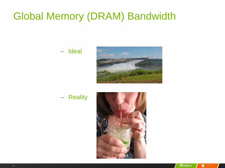
Global Memory (DRAM) Bandwidth
– Ideal
– Reality
4
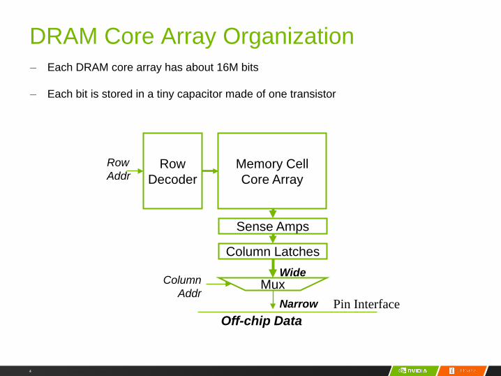
DRAM Core Array Organization– Each DRAM core array has about 16M bits
– Each bit is stored in a tiny capacitor made of one transistor
Memory CellCore Array
RowDecoder
Sense Amps
Column Latches
Mux
RowAddr
ColumnAddr
Off-chip Data
Wide
Narrow Pin Interface
5
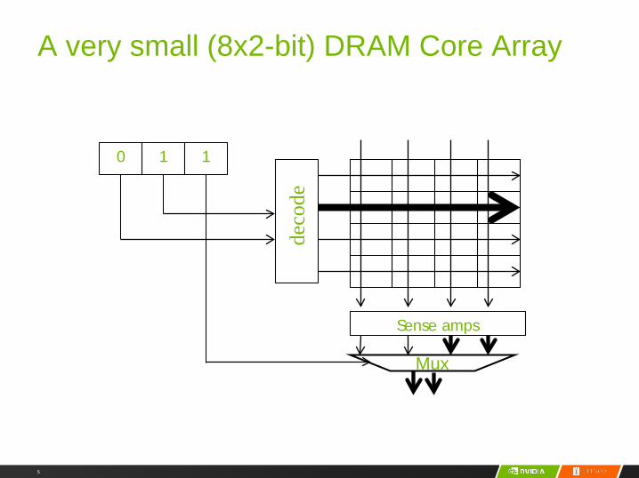
A very small (8x2-bit) DRAM Core Array
deco
de
0 1 1
Sense amps
Mux
6
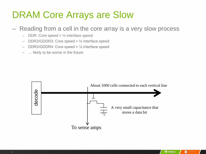
DRAM Core Arrays are Slow– Reading from a cell in the core array is a very slow process
– DDR: Core speed = ½ interface speed– DDR2/GDDR3: Core speed = ¼ interface speed– DDR3/GDDR4: Core speed = ⅛ interface speed– … likely to be worse in the future
deco
de
To sense amps
A very small capacitance that stores a data bit
About 1000 cells connected to each vertical line
7
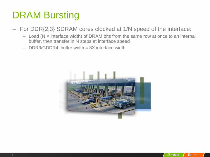
DRAM Bursting– For DDR{2,3} SDRAM cores clocked at 1/N speed of the interface:
– Load (N × interface width) of DRAM bits from the same row at once to an internal buffer, then transfer in N steps at interface speed
– DDR3/GDDR4: buffer width = 8X interface width
8
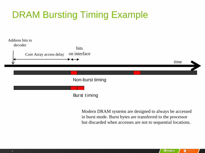
DRAM Bursting Timing Example
time
Address bits to decoder
Core Array access delaybits
on interface
Non-burst timing
Burst timing
Modern DRAM systems are designed to always be accessed in burst mode. Burst bytes are transferred to the processor but discarded when accesses are not to sequential locations.
9
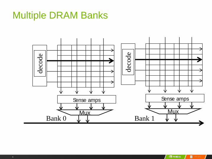
Multiple DRAM Banks
deco
de
Sense amps
Mux
deco
de
Sense amps
MuxBank 0 Bank 1
10
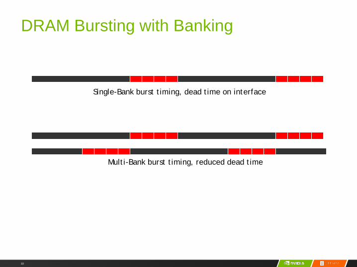
DRAM Bursting with Banking
Single-Bank burst timing, dead time on interface
Multi-Bank burst timing, reduced dead time
11
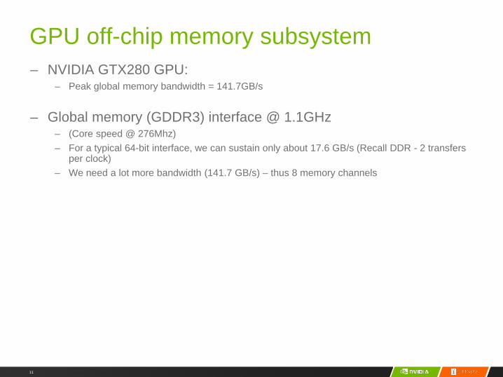
GPU off-chip memory subsystem– NVIDIA GTX280 GPU:
– Peak global memory bandwidth = 141.7GB/s
– Global memory (GDDR3) interface @ 1.1GHz– (Core speed @ 276Mhz)– For a typical 64-bit interface, we can sustain only about 17.6 GB/s (Recall DDR - 2 transfers
per clock)– We need a lot more bandwidth (141.7 GB/s) – thus 8 memory channels

GPU Teaching Kit
The GPU Teaching Kit is licensed by NVIDIA and the University of Illinois under the Creative Commons Attribution-NonCommercial 4.0 International License.

Memory Coalescing in CUDA
Lecture 6.2 – Performance Considerations
GPU Teaching KitAccelerated Computing
2
Objective– To learn that memory coalescing is important for effectively utilizing
memory bandwidth in CUDA– Its origin in DRAM burst– Checking if a CUDA memory access is coalesced– Techniques for improving memory coalescing in CUDA code
3
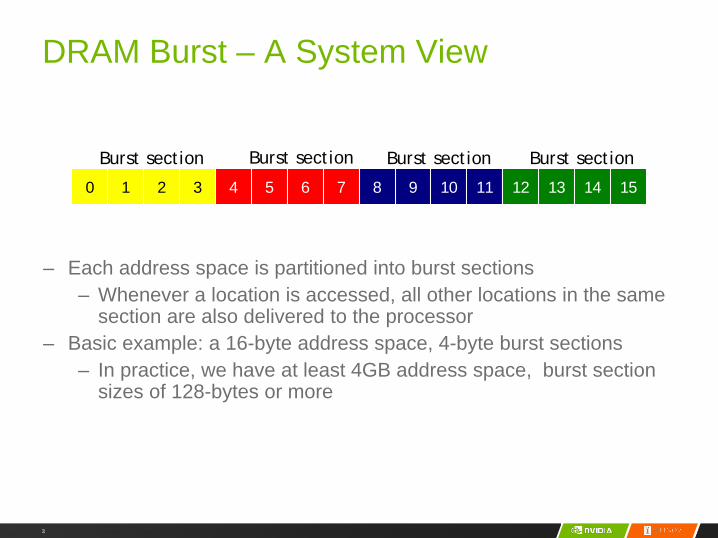
DRAM Burst – A System View
– Each address space is partitioned into burst sections – Whenever a location is accessed, all other locations in the same
section are also delivered to the processor – Basic example: a 16-byte address space, 4-byte burst sections
– In practice, we have at least 4GB address space, burst section sizes of 128-bytes or more
3
210 3 54 6 7 98 10 11 1312 14 15
Burst section Burst section Burst section Burst section
4
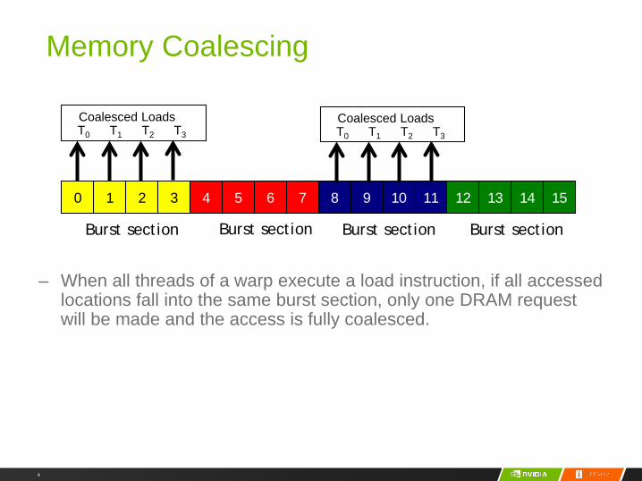
Memory Coalescing
– When all threads of a warp execute a load instruction, if all accessed locations fall into the same burst section, only one DRAM request will be made and the access is fully coalesced.
4
210 3 54 6 7 98 10 11 1312 14 15
Burst section Burst section Burst section Burst section
T0 T1 T2 T3
Coalesced LoadsT0 T1 T2 T3
Coalesced Loads
5
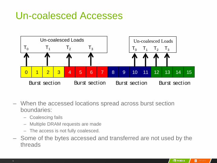
Un-coalesced Accesses
– When the accessed locations spread across burst section boundaries:
– Coalescing fails– Multiple DRAM requests are made– The access is not fully coalesced.
– Some of the bytes accessed and transferred are not used by the threads
5
210 3 54 6 7 98 10 11 1312 14 15
Burst section Burst section Burst section Burst section
T0 T1 T2 T3
Un-coalesced LoadsT0 T1 T2 T3
Un-coalesced Loads
6
How to judge if an access is coalesced?
– Accesses in a warp are to consecutive locations if the index in an array access is in the form of
– A[(expression with terms independent of threadIdx.x) + threadIdx.x];
6
7
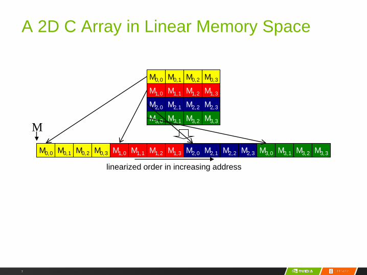
M0,2
M1,1
M0,1M0,0
M1,0
M0,3
M1,2 M1,3
M0,2M0,1M0,0 M0,3 M1,1M1,0 M1,2 M1,3 M2,1M2,0 M2,2 M2,3
M2,1M2,0 M2,2 M2,3
M3,1M3,0 M3,2 M3,3
M3,1M3,0 M3,2 M3,3
M
linearized order in increasing address
A 2D C Array in Linear Memory Space7
8
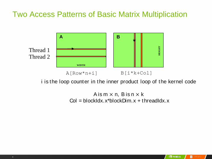
Two Access Patterns of Basic Matrix Multiplication
A B
WIDTH
Thread 1Thread 2
A[Row*n+i] B[i*k+Col]
i is the loop counter in the inner product loop of the kernel code
A is m × n, B is n × k Col = blockIdx.x*blockDim.x + threadIdx.x
HE
IGH
T
9
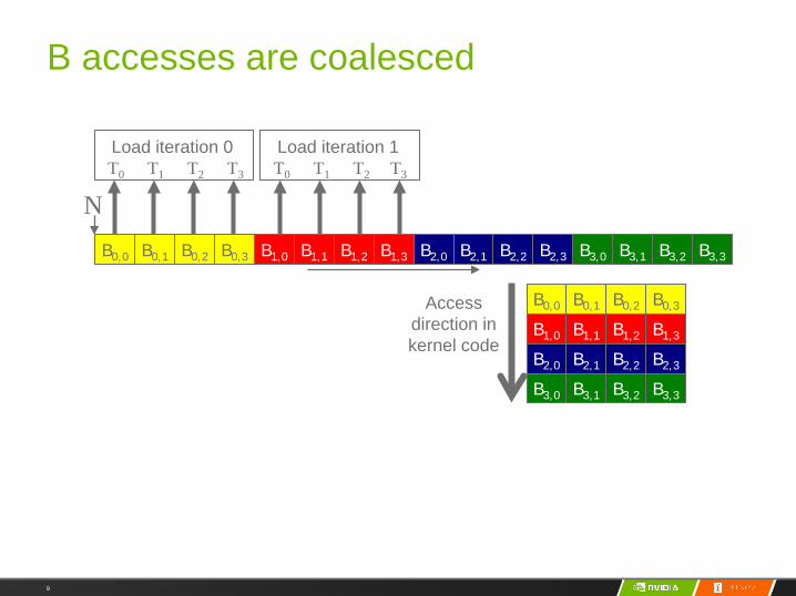
B accesses are coalesced
NT0 T1 T2 T3
Load iteration 0T0 T1 T2 T3
Load iteration 1
Access direction in kernel code
B0,2
B1,1
B0,1B0,0
B1,0
B0,3
B1,2 B1,3
B2,1B2,0 B2,2 B2,3
B3,1B3,0 B3,2 B3,3
B0,2B0,1B0,0 B0,3 B1,1B1,0 B1,2 B1,3 B2,1B2,0 B2,2 B2,3 B3,1B3,0 B3,2 B3,3
10
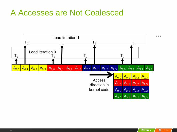
A Accesses are Not Coalesced
T0 T1 T2 T3Load iteration 0
T0 T1 T2 T3
Load iteration 1
Access direction in kernel code
…
A0,2
A1,1
A0,1A0,0
A1,0
A0,3
A1,2 A1,3
A2,1A2,0 A2,2 A2,3
A3,1A3,0 A3,2 A3,3
A0,2A0,1A0,0 A0,3 A1,1A1,0 A1,2 A1,3 A2,1A2,0 A2,2 A2,3 A3,1A3,0 A3,2 A3,3
11
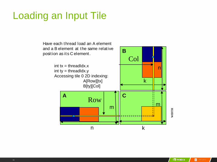
Loading an Input Tile
A
B
C
WID
TH
Row
Col
n
m
n
k
k
m
int tx = threadIdx.xint ty = threadIdx.yAccessing tile 0 2D indexing:
A[Row][tx]B[ty][Col]
Have each thread load an A element and a B element at the same relative position as its C element.
12
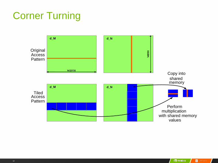
Corner Turning
d_M d_N
WID
TH
WIDTH
d_M d_N
Original AccessPattern
TiledAccessPattern
Copy into sharedmemory
Perform multiplication
with shared memory values
GPU Teaching Kit
The GPU Teaching Kit is licensed by NVIDIA and the University of Illinois under the Creative Commons Attribution-NonCommercial 4.0 International License.