user manual topor 6.1 - eremex
TRANSCRIPT

User ManualTopoR 6.1
.
July 2015
2 What’s New in TopoR (6.0 and 6.1)
2 6.1 July 2015
What’s New in TopoR (6.0 and 6.1)Version 6.0 was a major overhaul of how the system looked and worked. The current version 6.1continues and builds upon the changes introduced in the previous version.
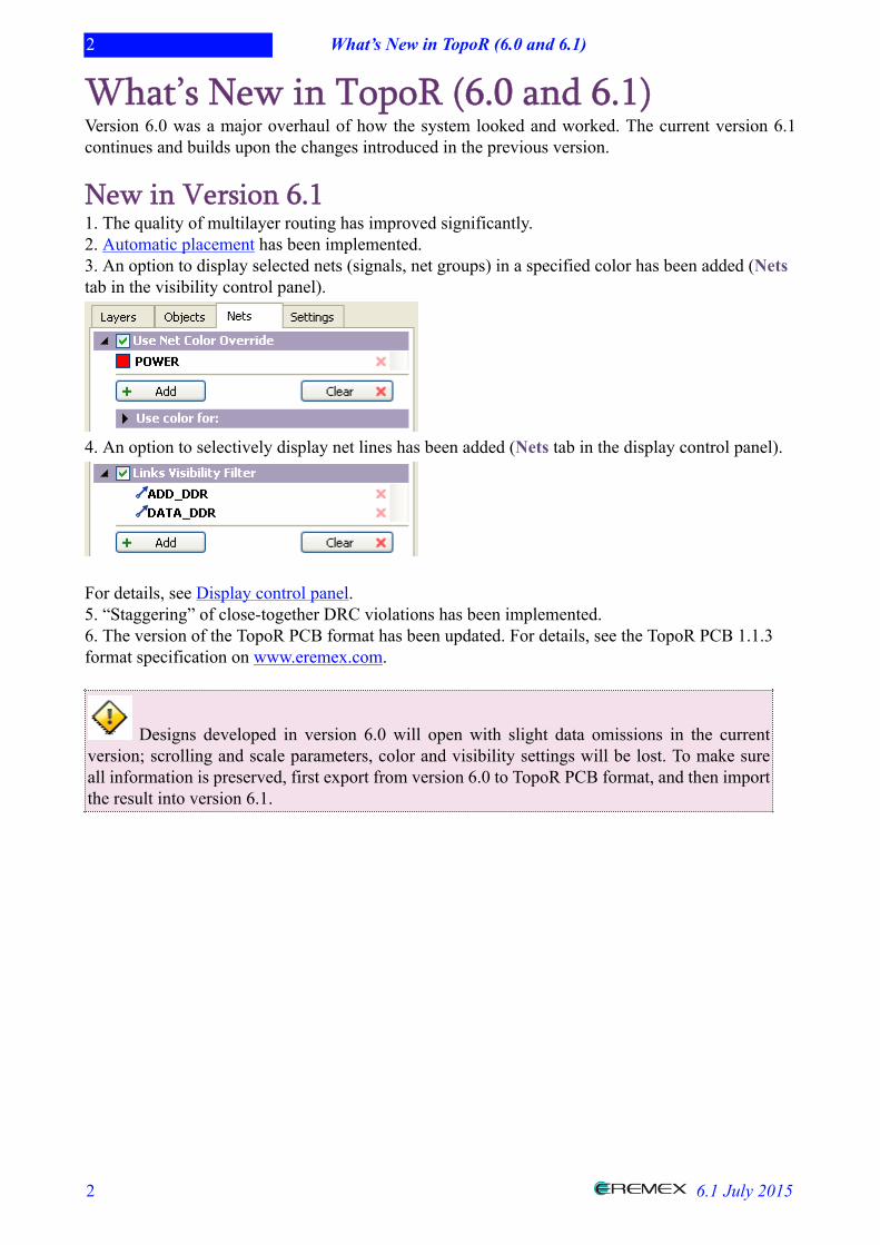
New in Version 6.11. The quality of multilayer routing has improved significantly.2. Automatic placement has been implemented.3. An option to display selected nets (signals, net groups) in a specified color has been added (Netstab in the visibility control panel).
4. An option to selectively display net lines has been added (Nets tab in the display control panel).
For details, see Display control panel.5. “Staggering” of close-together DRC violations has been implemented.6. The version of the TopoR PCB format has been updated. For details, see the TopoR PCB 1.1.3format specification on www.eremex.com.
Designs developed in version 6.0 will open with slight data omissions in the currentversion; scrolling and scale parameters, color and visibility settings will be lost. To make sureall information is preserved, first export from version 6.0 to TopoR PCB format, and then importthe result into version 6.1.
3 User Interface
3 6.1 July 2015
User Interface1.The program’s look has been updated. There have been some changes to the toolbars and mainmenu.2.The project control panel has been updated. The Project History tab has been added. Projects aresorted by opening date.3.The Open Containing Folder command in Windows Explorer opens the folder with the selectedfile. The Copy Project command copies all project files to a folder you specify.4.The autorouting control panel has been added, where you can select nets for routing and changeautorouting settings. The autorouting variant table is shown when you start autorouting.5.A control panel for the following automatic procedures has been added: calculation of wireshapes, wire route optimization, shifting of vias and components.6. The Options dialog box now includes the Hotkeys tab.7. Shortcut keys can be defined or redefined for most operations.
4 Topology Editor
4 6.1 July 2015
Topology Editor1. The editor toolbar has been updated. Related tools have been grouped. FreeStyle mode is nowone of the editor tools. A new tool has been added for measuring the distance between objects2. Arc-shaped wire segments are supported in all editor modes. In FreeStyle mode, multi-levelundo is supported.3. There is a new context menu, where all possible operations on selected objects are available.4. In manual wire routing mode, automatic searching and highlighting of wires in the currentlayer has been implemented. You can accept the suggested route (this routes the wire automatically)or ignore it and continue manual routing.5. The object selection filter has been updated and extended.6. You now have the choice to automatically remove vias that have become redundant due toautomatic procedures.7. Online DRC checks do not display bogus violations any more.
5 Design Properties Editor
5 6.1 July 2015
Design Properties Editor1. Automatic procedure settings have been moved from the editor to the corresponding toolbars.Editing settings have also been moved and are now available in the Editor Settings dialog box.2. Recently changed sections are now marked in the editor.3. The undo histories of the topology editor and the properties editor are now independent.

6 Autorouting
6 6.1 July 2015
Autorouting1. Piecemeal routing without fixing the wires’ geometric shape has been implemented.Previously laid out wires remain flexible while the optimal wire shape is calculated.2. Differential signals can now be split automatically.3. BGA routing has been enhanced in that it is now aware of impedors located under the BGAcomponent.

7 Other
7 6.1 July 2015
Other1. Data recovery after a crash has been implemented. If the crash occurred during autorouting,then autorouting results are also recovered.2. The TopoR PCB format has been updated. For details about the changes, see the specificationfor version 1.1.2 of the format.3. All designs developed in TopoR versions prior to 5.2 can be transferred to the current version.For that, export your design from the old version to the TopoR PCB format, and then import theresulting file into TopoR 6.0.

8 About the User Manual
8 6.1 July 2015
About the User ManualThis User Manual is made up of four major sections, A to D: introductory, main, auxiliary andreference. The introductory section contains only basic information about the TopoR system; all userswho have worked with previous versions of the software can safely skip it. The main section detailsthe use of TopoR and is intended for both beginners and experienced users. The Additional Featuressection describes functionality that only experienced users can take full advantage of. Finally, theReference is a collection of miscellaneous information that generally needs to be looked up.
Much of the manual’s content has seen considerable changes compared to the manual for version5.4. Some sections were redone (Creating a Project, Preferences, Editor Toolbar, Action Bar, ContextMenus, Selection Filter, Display Control, Data Recovery, Autorouting, Finding Variants, ConditionalRouting, Via Moving (F7)), because the functionality in question was either unavailable in priorversions or implemented in a markedly different way.

9 A. Before You Begin
9 6.1 July 2015
A. Before You BeginPart A of the manual is intended for users who are new to the TopoR CAD system. Here you willfind general information about the system and instructions on installing it and getting started.
10 General Information about TopoR
10 6.1 July 2015
General Information about TopoRThe TopoR (Topological Router) CAD system is a unique high-performance topological router forprinted circuit boards. It has the following distinctive features:# High routing speed and excellent routing quality# A robust toolset that considerably reduces design timesThis is achieved by the use of unique algorithms and an unconventional approach to solving complexproblems.
The PCB editor (topology editor) in TopoR features unique automatic procedures, including:# Calculating an efficient geometric shape for wires using topological paths# Moving components about a laid-out board without breaking the existing layout.
TopoR is compatible with a variety of CAD systems.# File import and export formats: ASCII (.pcb – PCAD ASCII PCB, .asc – PADS), DSN(.ses – Specctra and Electra), BRD (.brd – Eagle), HKP (Mentor Graphics Expedition)# Export-only formats: DXF, Gerber and Excellon (drill file).

11 Technical Details and Limitations
11 6.1 July 2015
Technical Details and LimitationsThe maximum number of routing layers varies from version to version.# Number of routing layers: 2 to 32# Total number of copper layers: up to 32# Precision: 0.1μm

12 Licensing
12 6.1 July 2015
LicensingThe primary (unlimited) TopoR UN license supports boards that contain up to 32 signal layers. Inaddition, several limited licenses are available:TopoR 2L Boards with up to 2 signal layers
TopoR 4L Boards with up to 4 signal layers
TopoR 8L Boards with up to 8 signal layers
TopoR 16L Boards with up to 16 signal layers
For information about purchasing, see the company website: http://eda.eremex.com/howtobuy/.
13 Contact Us
13 6.1 July 2015
Contact UsOOO "Eremex" Moscow, Profsoyuznaya ulitsa, 108. Phone.: +7 (495) 232-1864, Fax: +7 (495)234-0640
E-mail: [email protected], ICQ 464808130, Skype: supporteremex, Web: www.eremex.com
For information about purchasing the TopoR system, see http://eda.eremex.com/howtobuy/. Topurchase other software, write to [email protected].
We welcome any questions regarding the installation and use of our software, comments, bug reportsand enhancement suggestions at [email protected]. Also note that you can ask a question or searchfor an answer on the forum at http://forum.eremex.com/index.php?/forum/2-topor/
During one year following a license purchase, all customers receive free technical support thatincludes assistance at any design stage and software updates. To request technical support, [email protected]
In addition to this manual, you can find more information about TopoR in the FAQ section of ourwebsite: http://eda.eremex.com/support/faq.html
14 Installation
14 6.1 July 2015
Installation System Requirements
The following is the minimum hardware and software configuration.
# PC-compatible computer with an Intel® Pentium® III-1000 MHz processor or higher# Operating system: Microsoft® Windows® 2000 (SP3), XP (SP2 or SP3), Vista, Windows 7,Windows 8# Microsoft® Internet Explorer 5.0# Windows Installer 3.0 or higher# RAM: 512 MB# Free hard disk space: 100 MB# SVGA monitor and a graphics adapter, 256 colors, 1024x768.# Mouse with a scrolling wheel
Installing the Software on the Hard Drive
Do not connect the dongle before you have installed the dongle drivers.
1. Run the installer2. Follow the instructions.3. After the files have been copied, the dongle driver installer will start automatically.
After the dongle drivers have been installed, connect the dongle. In the folder you specify, theinstaller creates the BIN subfolder where the executable file are copied. The HELP subfolder containsdocumentation files. The EXAMPLES subfolder contains more subfolders with complete PCBproject files, one project per subfolder. Make sure you have write access to the newly-added folderswhen you work with the program.
The uninstaller is launched the conventional way (for example, using the Programs and Featuresfacility in the Control Panel). Uninstalling the program removes the BIN folder and all defaultexample files. If you want to keep them, copy the EXAMPLES folder elsewhere.
15 Getting Started
15 6.1 July 2015
Getting StartedWorking with PCBs in TopoR consists of the following steps:
1. Edit parameters2. Perform autorouting3. Edit topology manually4. Check for compliance with design rules5. Result output
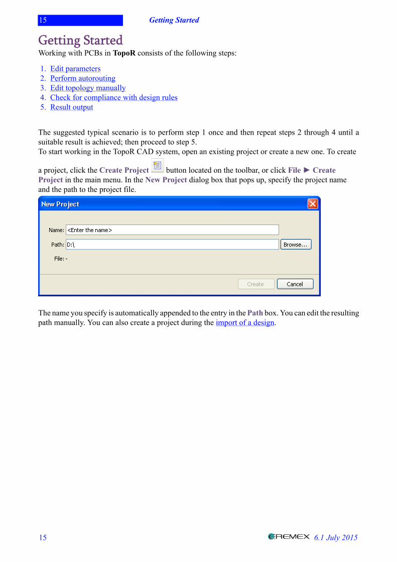
The suggested typical scenario is to perform step 1 once and then repeat steps 2 through 4 until asuitable result is achieved; then proceed to step 5.To start working in the TopoR CAD system, open an existing project or create a new one. To create
a project, click the Create Project button located on the toolbar, or click File ► CreateProject in the main menu. In the New Project dialog box that pops up, specify the project nameand the path to the project file.
The name you specify is automatically appended to the entry in the Path box. You can edit the resultingpath manually. You can also create a project during the import of a design.
16 Creating a Project
16 6.1 July 2015
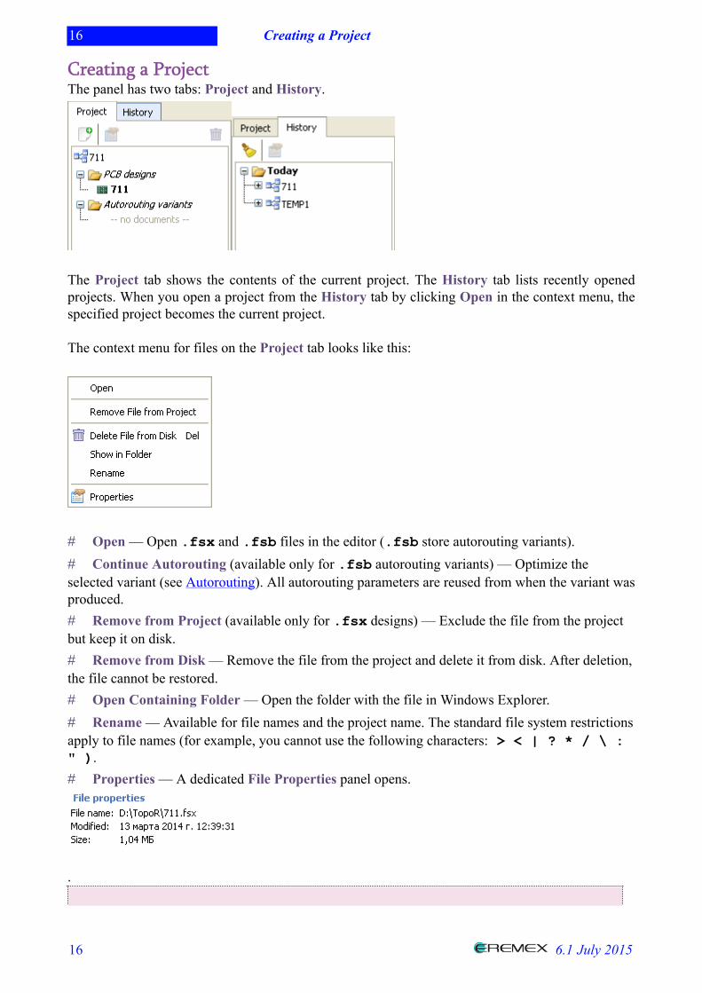
Creating a ProjectThe panel has two tabs: Project and History.
The Project tab shows the contents of the current project. The History tab lists recently openedprojects. When you open a project from the History tab by clicking Open in the context menu, thespecified project becomes the current project.
The context menu for files on the Project tab looks like this:
# Open — Open .fsx and .fsb files in the editor (.fsb store autorouting variants).# Continue Autorouting (available only for .fsb autorouting variants) — Optimize theselected variant (see Autorouting). All autorouting parameters are reused from when the variant wasproduced.# Remove from Project (available only for .fsx designs) — Exclude the file from the projectbut keep it on disk.# Remove from Disk — Remove the file from the project and delete it from disk. After deletion,the file cannot be restored.# Open Containing Folder — Open the folder with the file in Windows Explorer.# Rename — Available for file names and the project name. The standard file system restrictionsapply to file names (for example, you cannot use the following characters: > < | ? * / \ :" ).# Properties — A dedicated File Properties panel opens.
.
17 Creating a Project
17 6.1 July 2015
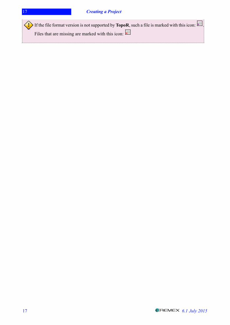
If the file format version is not supported by TopoR, such a file is marked with this icon: .
Files that are missing are marked with this icon:
18 Adding Files to the Project
18 6.1 July 2015
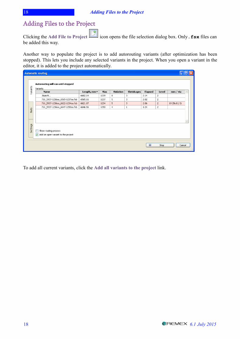
Adding Files to the Project
Clicking the Add File to Project icon opens the file selection dialog box. Only .fsx files canbe added this way.
Another way to populate the project is to add autorouting variants (after optimization has beenstopped). This lets you include any selected variants in the project. When you open a variant in theeditor, it is added to the project automatically.
To add all current variants, click the Add all variants to the project link.
19 Importing Designs
19 6.1 July 2015
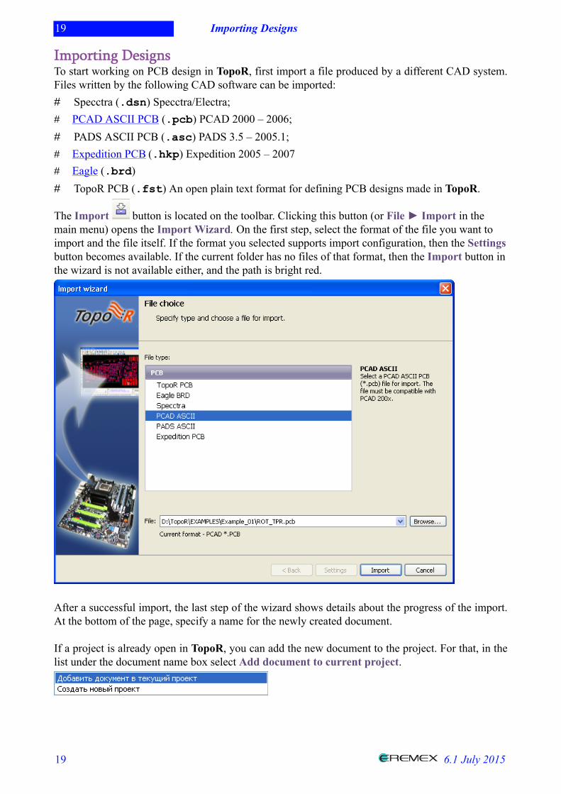
Importing DesignsTo start working on PCB design in TopoR, first import a file produced by a different CAD system.Files written by the following CAD software can be imported:# Specctra (.dsn) Specctra/Electra;# PCAD ASCII PCB (.pcb) PCAD 2000 – 2006;# PADS ASCII PCB (.asc) PADS 3.5 – 2005.1;# Expedition PCB (.hkp) Expedition 2005 – 2007# Eagle (.brd)# TopoR PCB (.fst) An open plain text format for defining PCB designs made in TopoR.
The Import button is located on the toolbar. Clicking this button (or File ► Import in themain menu) opens the Import Wizard. On the first step, select the format of the file you want toimport and the file itself. If the format you selected supports import configuration, then the Settingsbutton becomes available. If the current folder has no files of that format, then the Import button inthe wizard is not available either, and the path is bright red.
After a successful import, the last step of the wizard shows details about the progress of the import.At the bottom of the page, specify a name for the newly created document.
If a project is already open in TopoR, you can add the new document to the project. For that, in thelist under the document name box select Add document to current project.
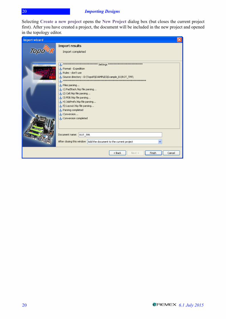
20 Importing Designs
20 6.1 July 2015
Selecting Create a new project opens the New Project dialog box (but closes the current projectfirst). After you have created a project, the document will be included in the new project and openedin the topology editor.
21 Preferences
21 6.1 July 2015
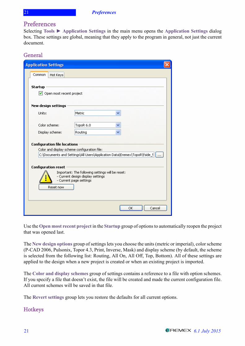
PreferencesSelecting Tools ► Application Settings in the main menu opens the Application Settings dialogbox. These settings are global, meaning that they apply to the program in general, not just the currentdocument.
General
Use the Open most recent project in the Startup group of options to automatically reopen the projectthat was opened last.
The New design options group of settings lets you choose the units (metric or imperial), color scheme(P-CAD 2006, Pulsonix, Topor 4.3, Print, Inverse, Mask) and display scheme (by default, the schemeis selected from the following list: Routing, All On, All Off, Top, Bottom). All of these settings areapplied to the design when a new project is created or when an existing project is imported.
The Color and display schemes group of settings contains a reference to a file with option schemes.If you specify a file that doesn’t exist, the file will be created and made the current configuration file.All current schemes will be saved in that file.
The Revert settings group lets you restore the defaults for all current options.
Hotkeys
22 Preferences
22 6.1 July 2015
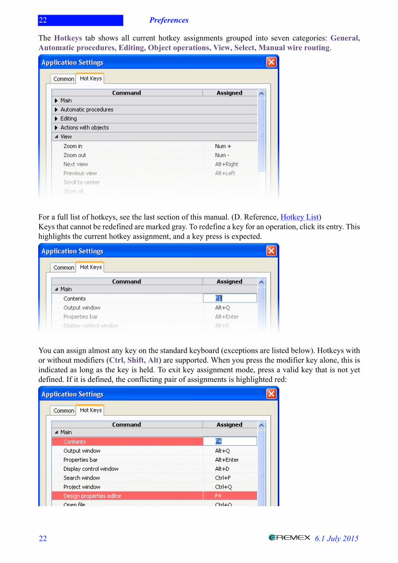
The Hotkeys tab shows all current hotkey assignments grouped into seven categories: General,Automatic procedures, Editing, Object operations, View, Select, Manual wire routing.
For a full list of hotkeys, see the last section of this manual. (D. Reference, Hotkey List)Keys that cannot be redefined are marked gray. To redefine a key for an operation, click its entry. Thishighlights the current hotkey assignment, and a key press is expected.
You can assign almost any key on the standard keyboard (exceptions are listed below). Hotkeys withor without modifiers (Ctrl, Shift, Alt) are supported. When you press the modifier key alone, this isindicated as long as the key is held. To exit key assignment mode, press a valid key that is not yetdefined. If it is defined, the conflicting pair of assignments is highlighted red:
23 Preferences
23 6.1 July 2015
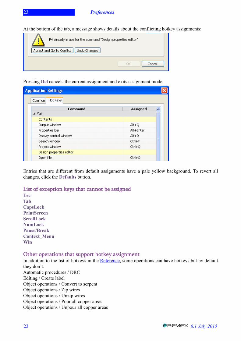
At the bottom of the tab, a message shows details about the conflicting hotkey assignments:
Pressing Del cancels the current assignment and exits assignment mode.
Entries that are different from default assignments have a pale yellow background. To revert allchanges, click the Defaults button.
List of exception keys that cannot be assignedEscTabCapsLockPrintScreenScrollLockNumLockPause/BreakContext_MenuWin
Other operations that support hotkey assignmentIn addition to the list of hotkeys in the Reference, some operations can have hotkeys but by defaultthey don’t.Automatic procedures / DRCEditing / Create labelObject operations / Convert to serpentObject operations / Zip wiresObject operations / Unzip wiresObject operations / Pour all copper areasObject operations / Unpour all copper areas
24 Preferences
24 6.1 July 2015
Object operations / Repour all copper areasView / CenterView / Show allView / Metal layers on/offView / Copper areas on/offView / Grid on/offView / Wires on/offView / Vias on/offView / Only active layer on/offView / Keepouts on/offSelect / Invert selectionDisplay schemes / RoutingDisplay schemes / All onDisplay schemes / All offDisplay schemes / TopDisplay schemes / BottomColor schemes / P-CAD 2006Color schemes / PulsonixColor schemes / Topor 4.3Color schemes / PrintColor schemes / InverseColor schemes / Mask
Note that a hotkey can be assigned for any display scheme.
25 B. Getting Started with Designing in TopoR
25 6.1 July 2015
B. Getting Started with Designing in TopoRThis part of the manual is the most important one. The sections contained in it are intended forengineers and other specialists working on PCB design and using TopoR. The information includedis sufficient for becoming productive with the system.
26 Editing Parameters
26 6.1 July 2015
Editing ParametersDesign parameters include:# The layer stack# Padstacks# Types of vias# Rules for automatic and manual routingIn addition, this section of the manual describes object grouping and configuration editing.
The High-speed rules panel of the properties editor is described in part C, in the section about high-speed appliances.
27 General
27 6.1 July 2015
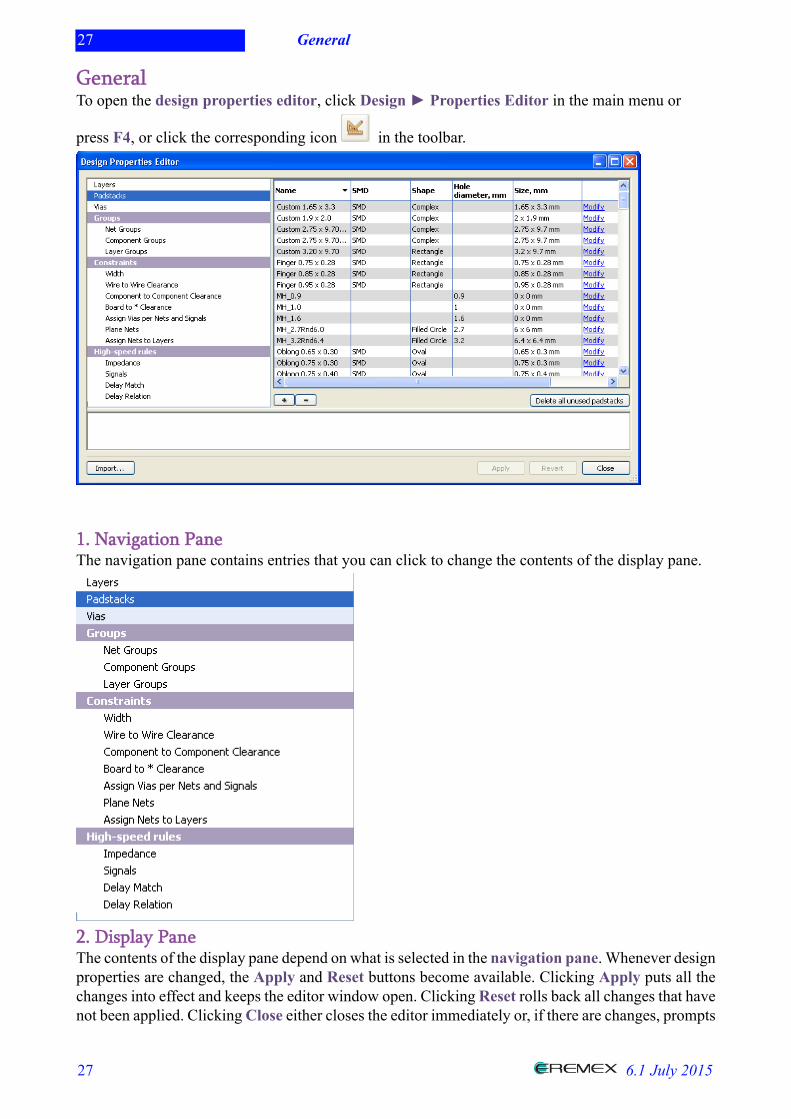
GeneralTo open the design properties editor, click Design ► Properties Editor in the main menu or
press F4, or click the corresponding icon in the toolbar.
1. Navigation PaneThe navigation pane contains entries that you can click to change the contents of the display pane.
2. Display PaneThe contents of the display pane depend on what is selected in the navigation pane. Whenever designproperties are changed, the Apply and Reset buttons become available. Clicking Apply puts all thechanges into effect and keeps the editor window open. Clicking Reset rolls back all changes that havenot been applied. Clicking Close either closes the editor immediately or, if there are changes, prompts
28 General
28 6.1 July 2015
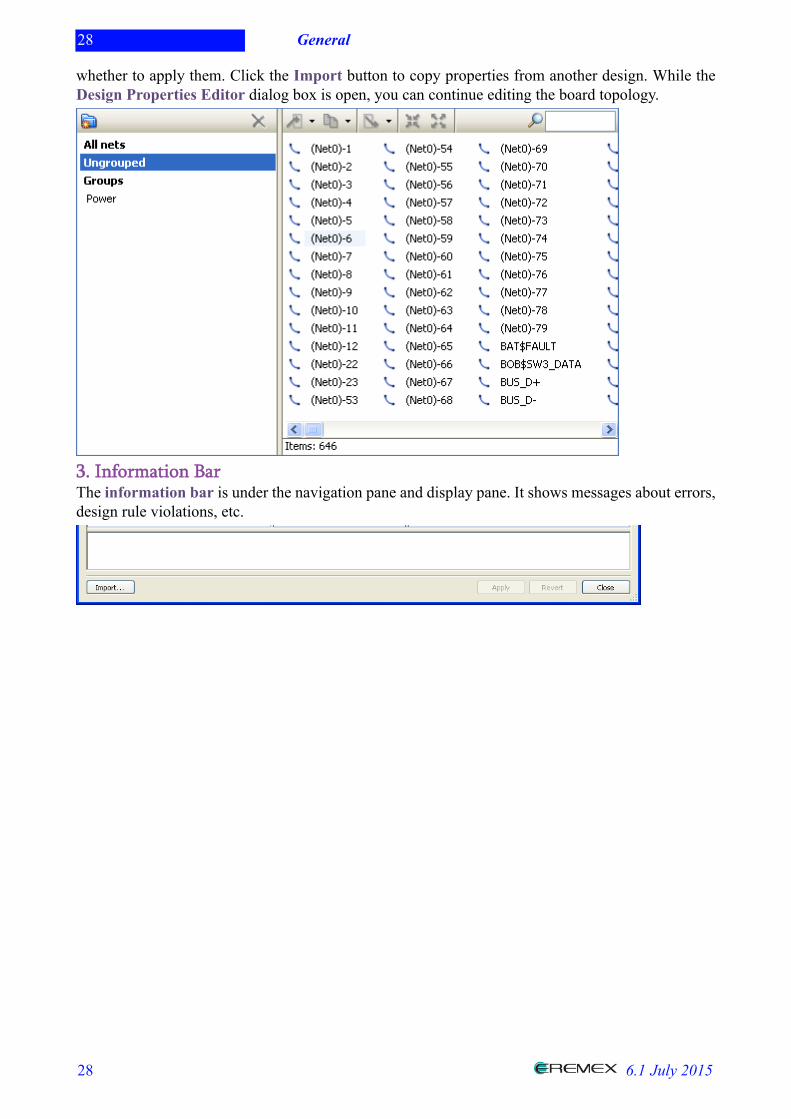
whether to apply them. Click the Import button to copy properties from another design. While theDesign Properties Editor dialog box is open, you can continue editing the board topology.
3. Information BarThe information bar is under the navigation pane and display pane. It shows messages about errors,design rule violations, etc.
29 Importing Properties
29 6.1 July 2015
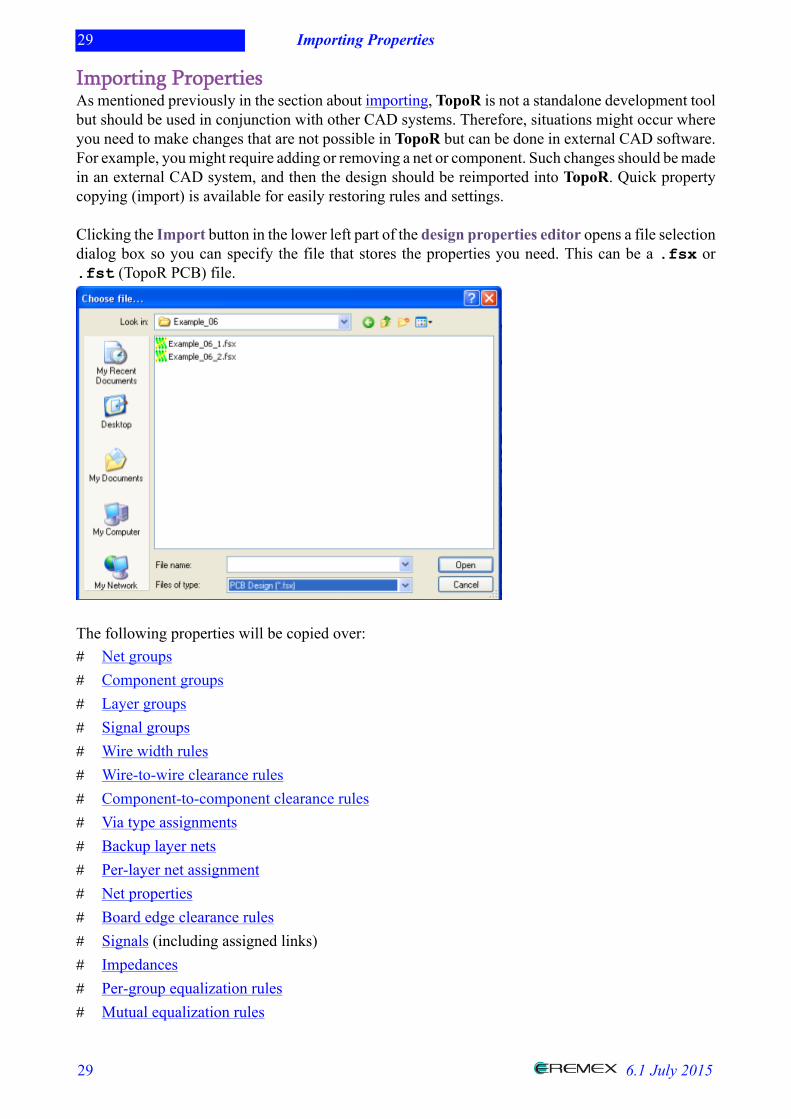
Importing PropertiesAs mentioned previously in the section about importing, TopoR is not a standalone development toolbut should be used in conjunction with other CAD systems. Therefore, situations might occur whereyou need to make changes that are not possible in TopoR but can be done in external CAD software.For example, you might require adding or removing a net or component. Such changes should be madein an external CAD system, and then the design should be reimported into TopoR. Quick propertycopying (import) is available for easily restoring rules and settings.
Clicking the Import button in the lower left part of the design properties editor opens a file selectiondialog box so you can specify the file that stores the properties you need. This can be a .fsx or.fst (TopoR PCB) file.
The following properties will be copied over:# Net groups# Component groups# Layer groups# Signal groups# Wire width rules# Wire-to-wire clearance rules# Component-to-component clearance rules# Via type assignments# Backup layer nets# Per-layer net assignment# Net properties# Board edge clearance rules# Signals (including assigned links)# Impedances# Per-group equalization rules# Mutual equalization rules

30 Importing Properties
30 6.1 July 2015
All current properties are removed. If the design defines width rules that are not present in the specifiedfile, they are also removed.
31 Layers
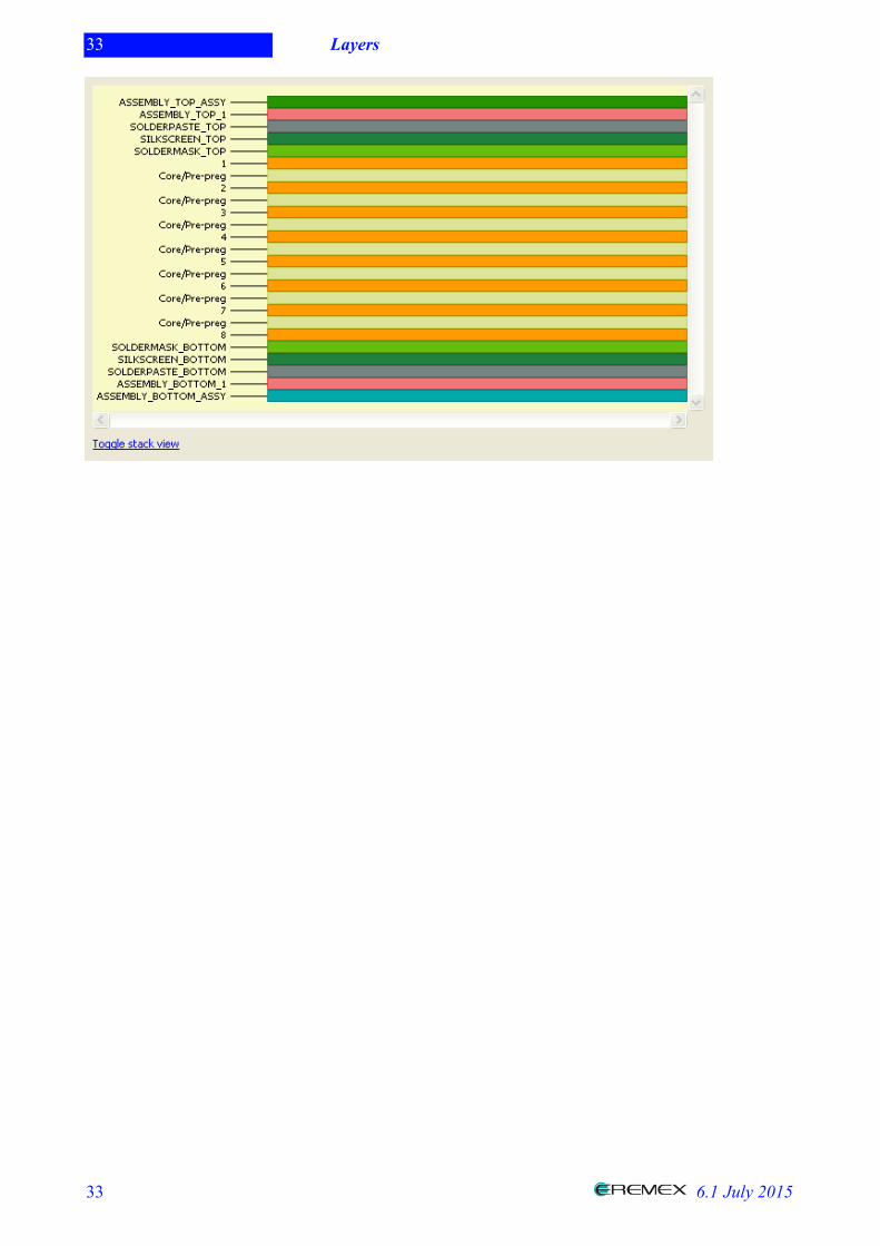
31 6.1 July 2015
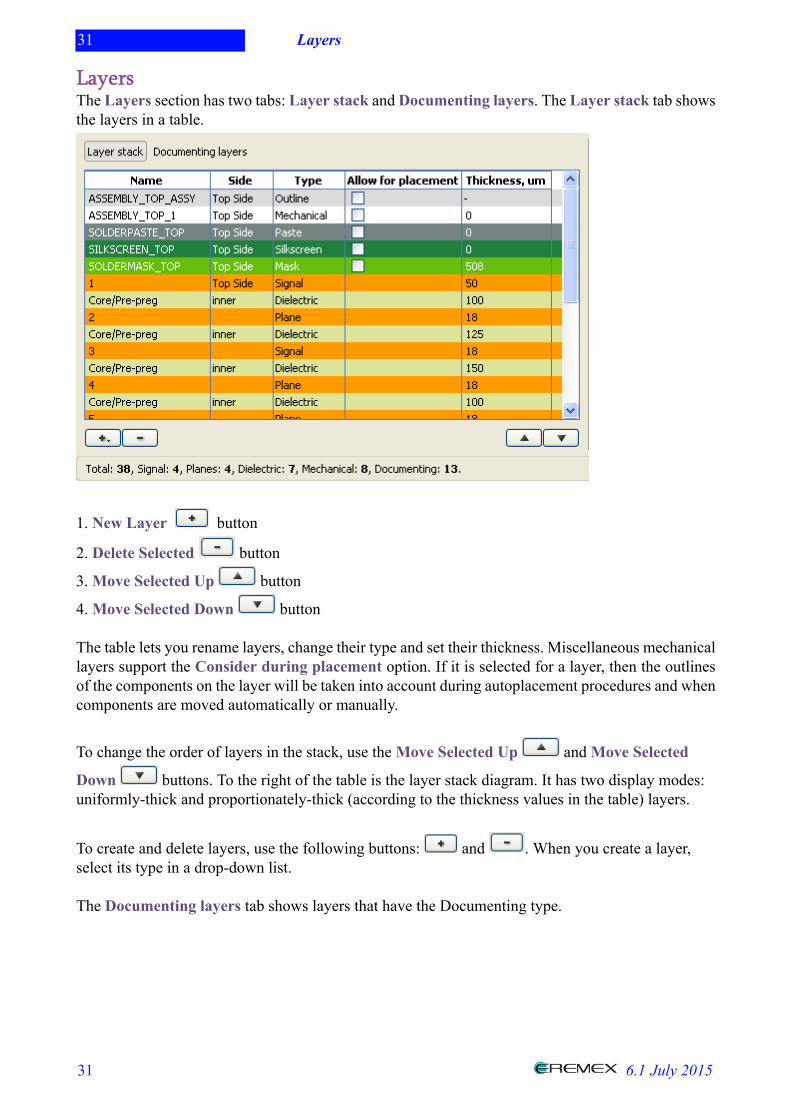
LayersThe Layers section has two tabs: Layer stack and Documenting layers. The Layer stack tab showsthe layers in a table.
1. New Layer button
2. Delete Selected button
3. Move Selected Up button
4. Move Selected Down button
The table lets you rename layers, change their type and set their thickness. Miscellaneous mechanicallayers support the Consider during placement option. If it is selected for a layer, then the outlinesof the components on the layer will be taken into account during autoplacement procedures and whencomponents are moved automatically or manually.
To change the order of layers in the stack, use the Move Selected Up and Move Selected
Down buttons. To the right of the table is the layer stack diagram. It has two display modes:uniformly-thick and proportionately-thick (according to the thickness values in the table) layers.
To create and delete layers, use the following buttons: and . When you create a layer,select its type in a drop-down list.
The Documenting layers tab shows layers that have the Documenting type.
32 Layers
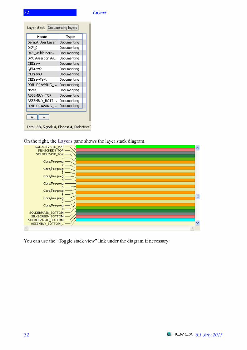
32 6.1 July 2015
On the right, the Layers pane shows the layer stack diagram.
You can use the “Toggle stack view” link under the diagram if necessary:
33 Layers
33 6.1 July 2015
34 Padstacks
34 6.1 July 2015
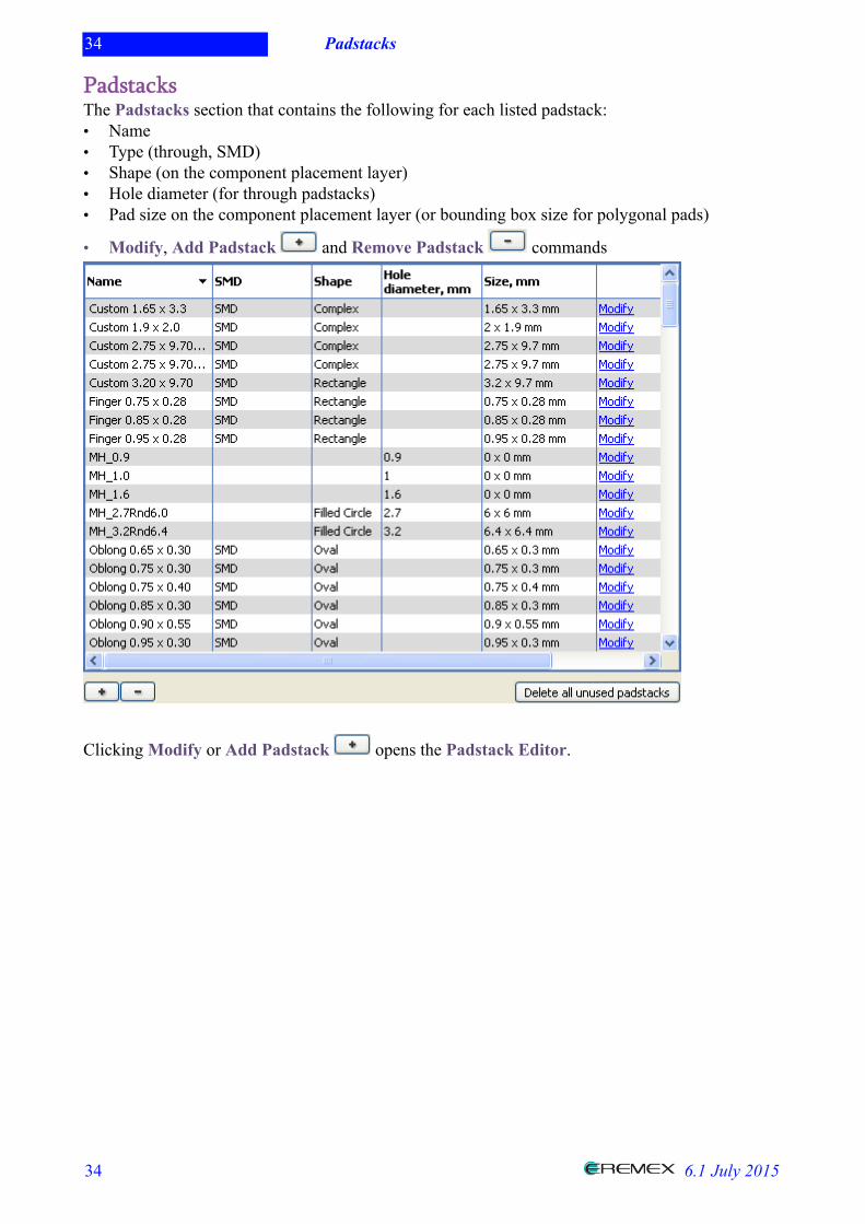
PadstacksThe Padstacks section that contains the following for each listed padstack:• Name• Type (through, SMD)• Shape (on the component placement layer)• Hole diameter (for through padstacks)• Pad size on the component placement layer (or bounding box size for polygonal pads)
• Modify, Add Padstack and Remove Padstack commands
Clicking Modify or Add Padstack opens the Padstack Editor.
35 Padstacks
35 6.1 July 2015
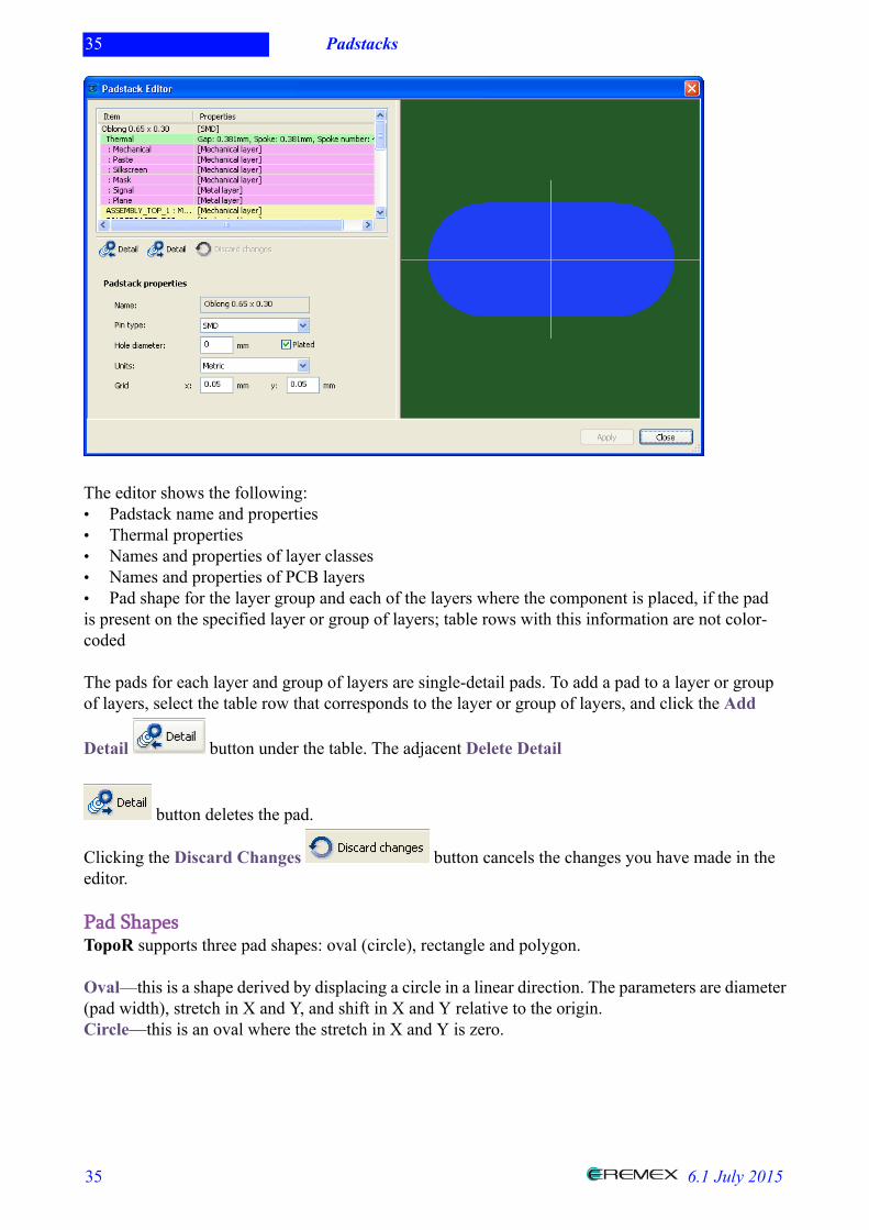
The editor shows the following:• Padstack name and properties• Thermal properties• Names and properties of layer classes• Names and properties of PCB layers• Pad shape for the layer group and each of the layers where the component is placed, if the padis present on the specified layer or group of layers; table rows with this information are not color-coded
The pads for each layer and group of layers are single-detail pads. To add a pad to a layer or groupof layers, select the table row that corresponds to the layer or group of layers, and click the Add
Detail button under the table. The adjacent Delete Detail
button deletes the pad.
Clicking the Discard Changes button cancels the changes you have made in theeditor.
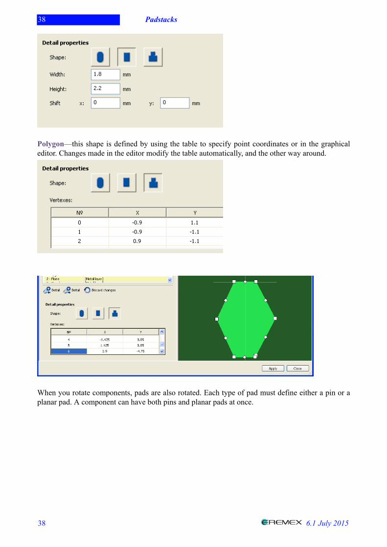
Pad ShapesTopoR supports three pad shapes: oval (circle), rectangle and polygon.
Oval—this is a shape derived by displacing a circle in a linear direction. The parameters are diameter(pad width), stretch in X and Y, and shift in X and Y relative to the origin.Circle—this is an oval where the stretch in X and Y is zero.
36 Padstacks
36 6.1 July 2015
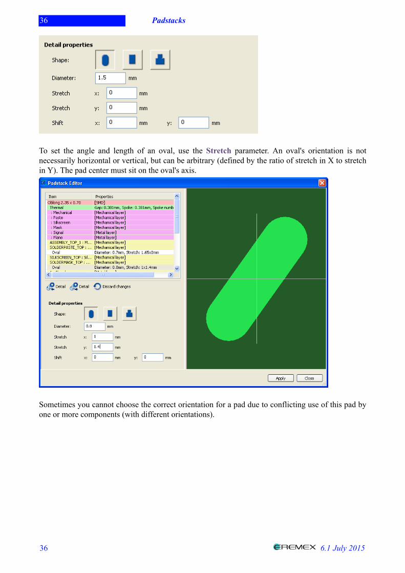
To set the angle and length of an oval, use the Stretch parameter. An oval's orientation is notnecessarily horizontal or vertical, but can be arbitrary (defined by the ratio of stretch in X to stretchin Y). The pad center must sit on the oval's axis.
Sometimes you cannot choose the correct orientation for a pad due to conflicting use of this pad byone or more components (with different orientations).
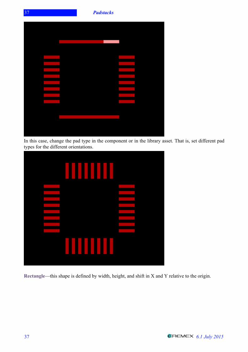
37 Padstacks
37 6.1 July 2015
In this case, change the pad type in the component or in the library asset. That is, set different padtypes for the different orientations.
Rectangle—this shape is defined by width, height, and shift in X and Y relative to the origin.
38 Padstacks
38 6.1 July 2015
Polygon—this shape is defined by using the table to specify point coordinates or in the graphicaleditor. Changes made in the editor modify the table automatically, and the other way around.
When you rotate components, pads are also rotated. Each type of pad must define either a pin or aplanar pad. A component can have both pins and planar pads at once.
39 Vias
39 6.1 July 2015
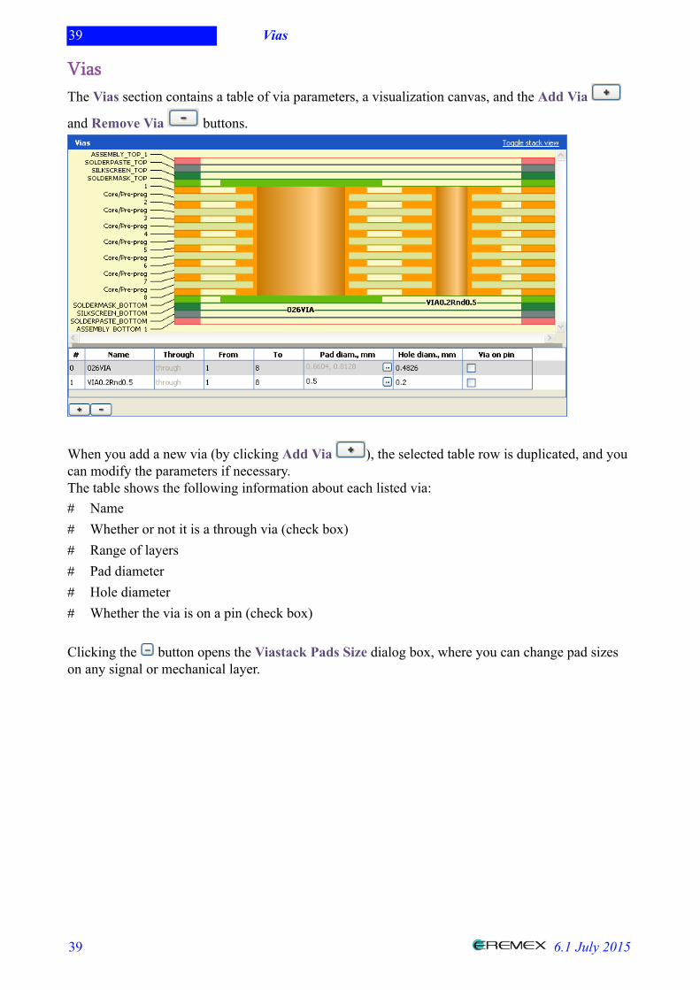
ViasThe Vias section contains a table of via parameters, a visualization canvas, and the Add Via
and Remove Via buttons.
When you add a new via (by clicking Add Via ), the selected table row is duplicated, and youcan modify the parameters if necessary.The table shows the following information about each listed via:# Name# Whether or not it is a through via (check box)# Range of layers# Pad diameter# Hole diameter# Whether the via is on a pin (check box)
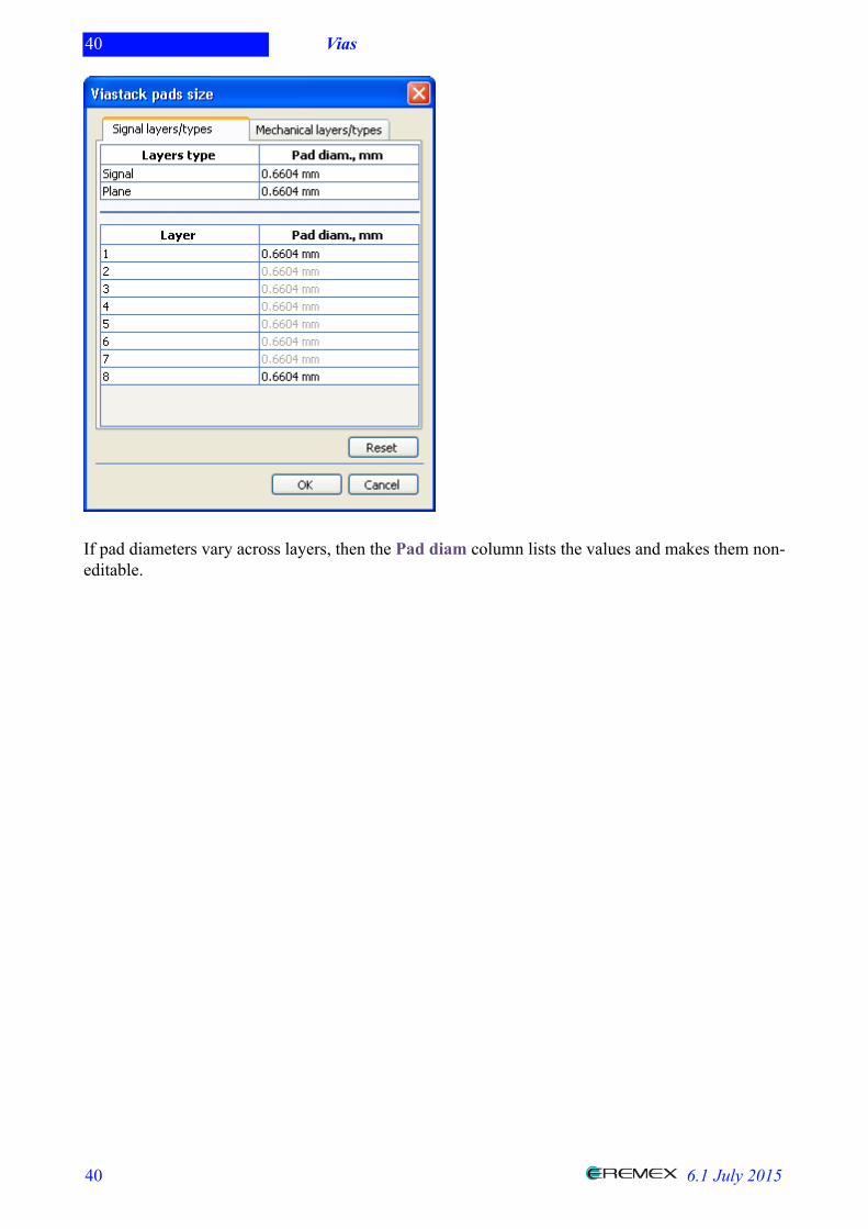
Clicking the button opens the Viastack Pads Size dialog box, where you can change pad sizeson any signal or mechanical layer.
40 Vias
40 6.1 July 2015
If pad diameters vary across layers, then the Pad diam column lists the values and makes them non-editable.
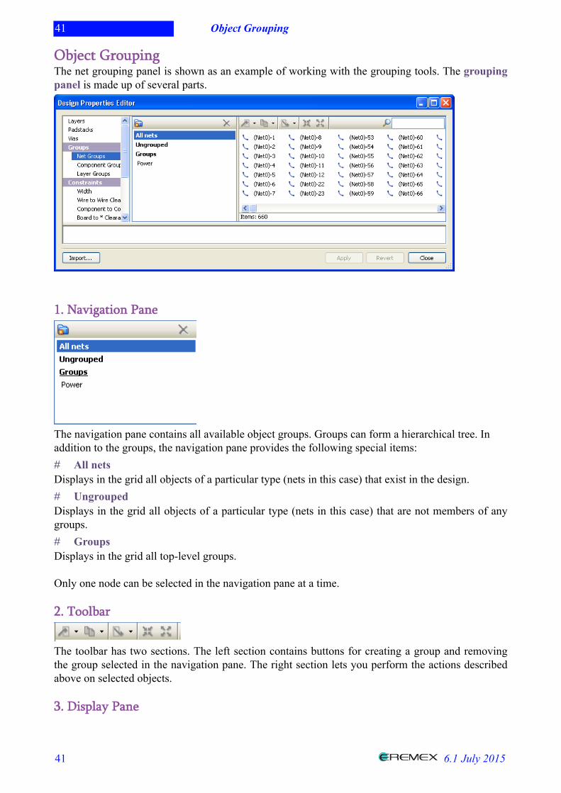
41 Object Grouping
41 6.1 July 2015
Object GroupingThe net grouping panel is shown as an example of working with the grouping tools. The groupingpanel is made up of several parts.
1. Navigation Pane
The navigation pane contains all available object groups. Groups can form a hierarchical tree. Inaddition to the groups, the navigation pane provides the following special items:# All netsDisplays in the grid all objects of a particular type (nets in this case) that exist in the design.# UngroupedDisplays in the grid all objects of a particular type (nets in this case) that are not members of anygroups.# GroupsDisplays in the grid all top-level groups.
Only one node can be selected in the navigation pane at a time.
2. Toolbar
The toolbar has two sections. The left section contains buttons for creating a group and removingthe group selected in the navigation pane. The right section lets you perform the actions describedabove on selected objects.
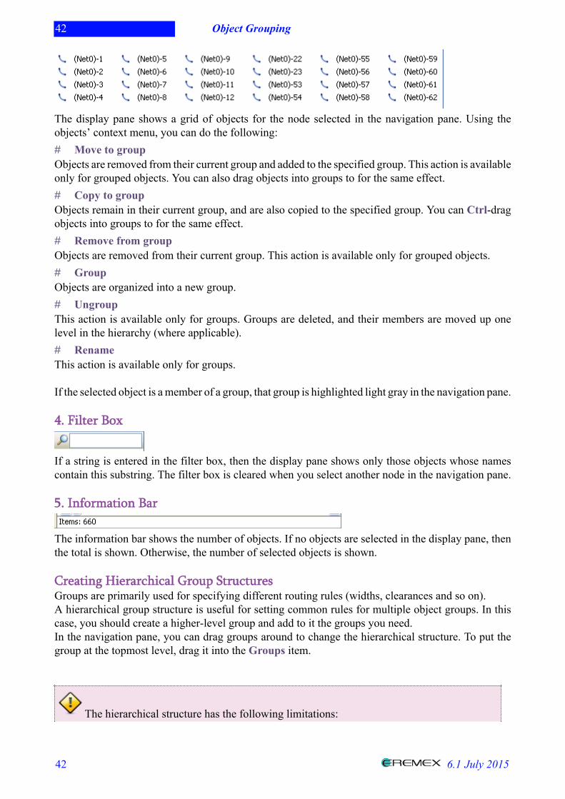
3. Display Pane
42 Object Grouping
42 6.1 July 2015
The display pane shows a grid of objects for the node selected in the navigation pane. Using theobjects’ context menu, you can do the following:# Move to groupObjects are removed from their current group and added to the specified group. This action is availableonly for grouped objects. You can also drag objects into groups to for the same effect.# Copy to groupObjects remain in their current group, and are also copied to the specified group. You can Ctrl-dragobjects into groups to for the same effect.# Remove from groupObjects are removed from their current group. This action is available only for grouped objects.# GroupObjects are organized into a new group.# UngroupThis action is available only for groups. Groups are deleted, and their members are moved up onelevel in the hierarchy (where applicable).# RenameThis action is available only for groups.
If the selected object is a member of a group, that group is highlighted light gray in the navigation pane.
4. Filter Box
If a string is entered in the filter box, then the display pane shows only those objects whose namescontain this substring. The filter box is cleared when you select another node in the navigation pane.
5. Information Bar
The information bar shows the number of objects. If no objects are selected in the display pane, thenthe total is shown. Otherwise, the number of selected objects is shown.
Creating Hierarchical Group StructuresGroups are primarily used for specifying different routing rules (widths, clearances and so on).A hierarchical group structure is useful for setting common rules for multiple object groups. In thiscase, you should create a higher-level group and add to it the groups you need.In the navigation pane, you can drag groups around to change the hierarchical structure. To put thegroup at the topmost level, drag it into the Groups item.
The hierarchical structure has the following limitations:
43 Object Grouping
43 6.1 July 2015
1. A group cannot be a member of more than one other group.2. Groups at the topmost level cannot be members of other groups.
44 Constraints
44 6.1 July 2015
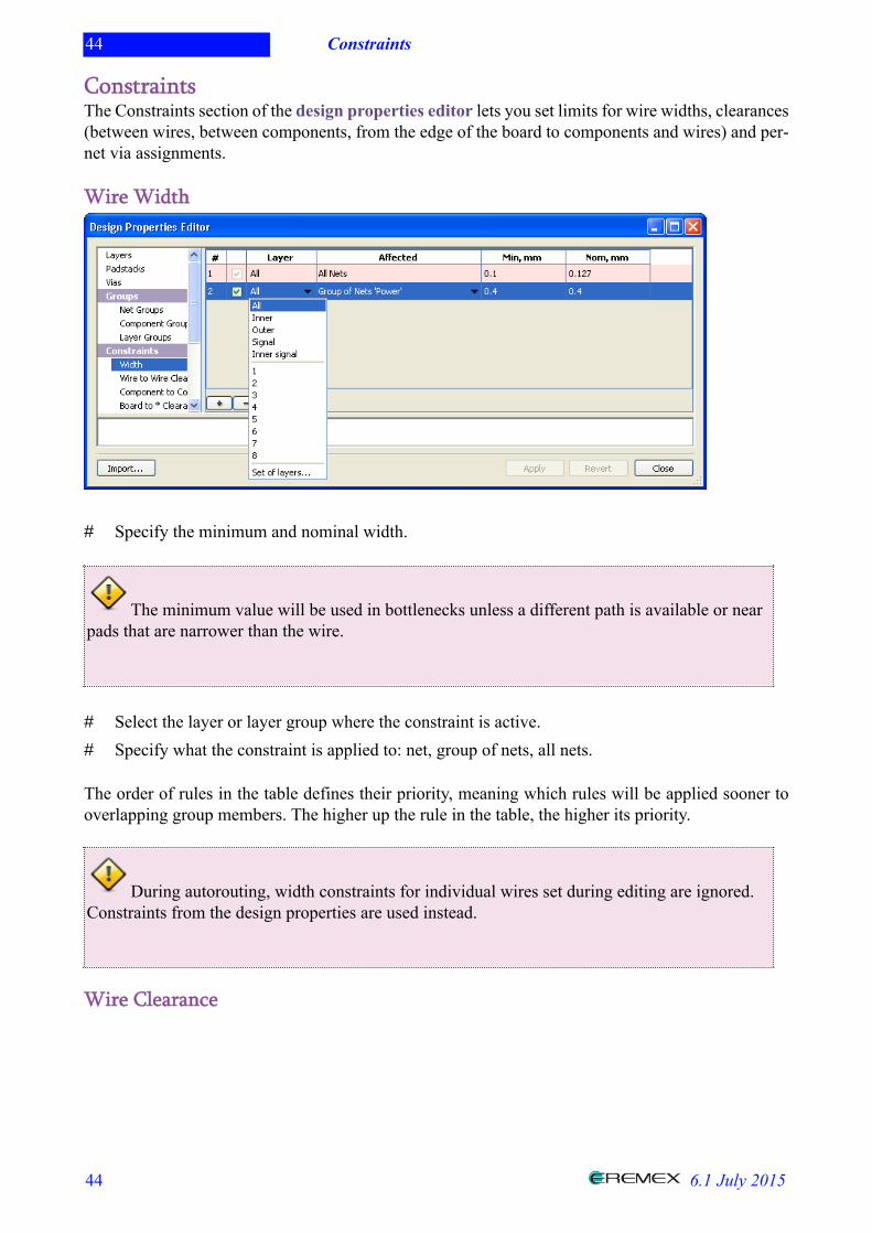
ConstraintsThe Constraints section of the design properties editor lets you set limits for wire widths, clearances(between wires, between components, from the edge of the board to components and wires) and per-net via assignments.
Wire Width
# Specify the minimum and nominal width.
The minimum value will be used in bottlenecks unless a different path is available or nearpads that are narrower than the wire.
# Select the layer or layer group where the constraint is active.# Specify what the constraint is applied to: net, group of nets, all nets.
The order of rules in the table defines their priority, meaning which rules will be applied sooner tooverlapping group members. The higher up the rule in the table, the higher its priority.
During autorouting, width constraints for individual wires set during editing are ignored.Constraints from the design properties are used instead.
Wire Clearance
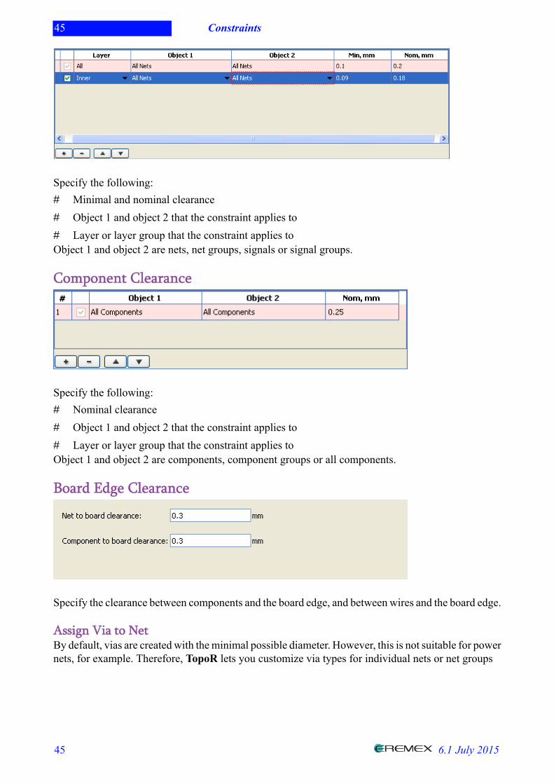
45 Constraints
45 6.1 July 2015
Specify the following:# Minimal and nominal clearance# Object 1 and object 2 that the constraint applies to# Layer or layer group that the constraint applies toObject 1 and object 2 are nets, net groups, signals or signal groups.
Component Clearance
Specify the following:# Nominal clearance# Object 1 and object 2 that the constraint applies to# Layer or layer group that the constraint applies toObject 1 and object 2 are components, component groups or all components. Board Edge Clearance
Specify the clearance between components and the board edge, and between wires and the board edge.
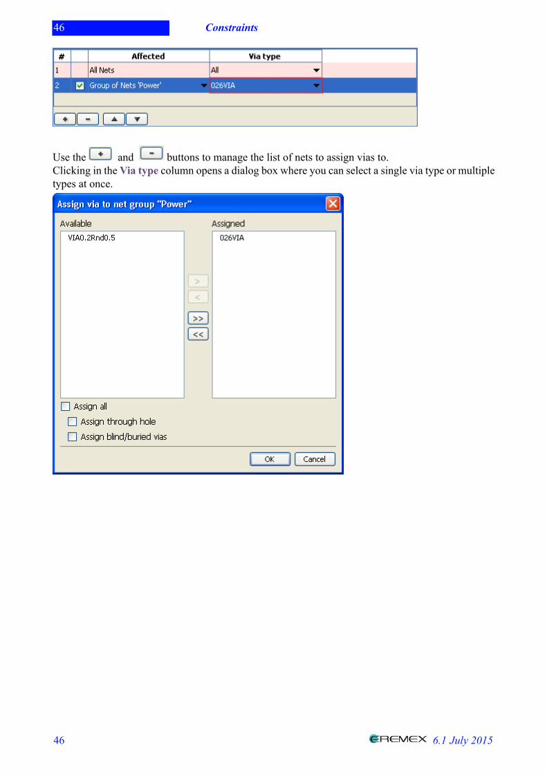
Assign Via to NetBy default, vias are created with the minimal possible diameter. However, this is not suitable for powernets, for example. Therefore, TopoR lets you customize via types for individual nets or net groups
46 Constraints
46 6.1 July 2015
Use the and buttons to manage the list of nets to assign vias to.Clicking in the Via type column opens a dialog box where you can select a single via type or multipletypes at once.
47 Autorouting
47 6.1 July 2015
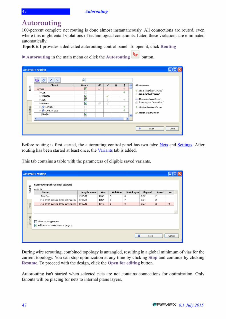
Autorouting100-percent complete net routing is done almost instantaneously. All connections are routed, evenwhere this might entail violations of technological constraints. Later, these violations are eliminatedautomatically.TopoR 6.1 provides a dedicated autorouting control panel. To open it, click Routing
►Autorouting in the main menu or click the Autorouting button.
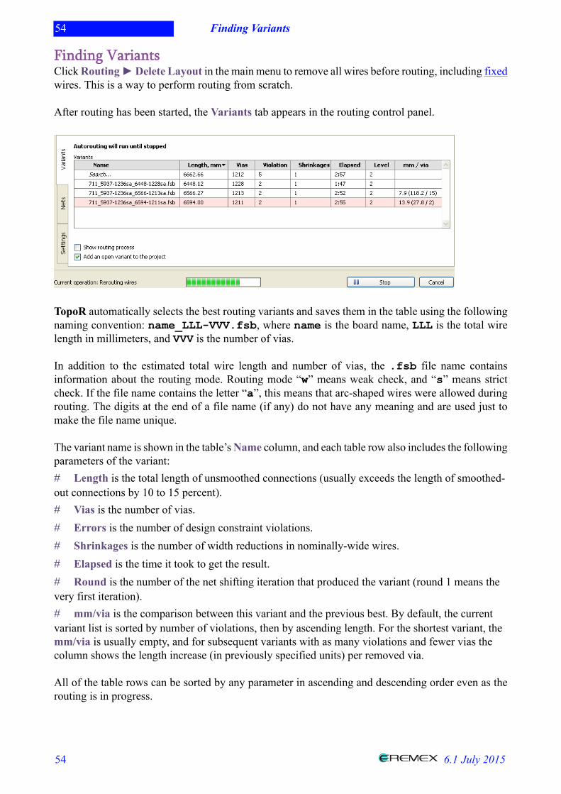
Before routing is first started, the autorouting control panel has two tabs: Nets and Settings. Afterrouting has been started at least once, the Variants tab is added.
This tab contains a table with the parameters of eligible saved variants.
During wire rerouting, combined topology is untangled, resulting in a global minimum of vias for thecurrent topology. You can stop optimization at any time by clicking Stop and continue by clickingResume. To proceed with the design, click the Open for editing button.
Autorouting isn't started when selected nets are not contains connections for optimization. Onlyfanouts will be placing for nets to internal plane layers.
48 Autorouting
48 6.1 July 2015
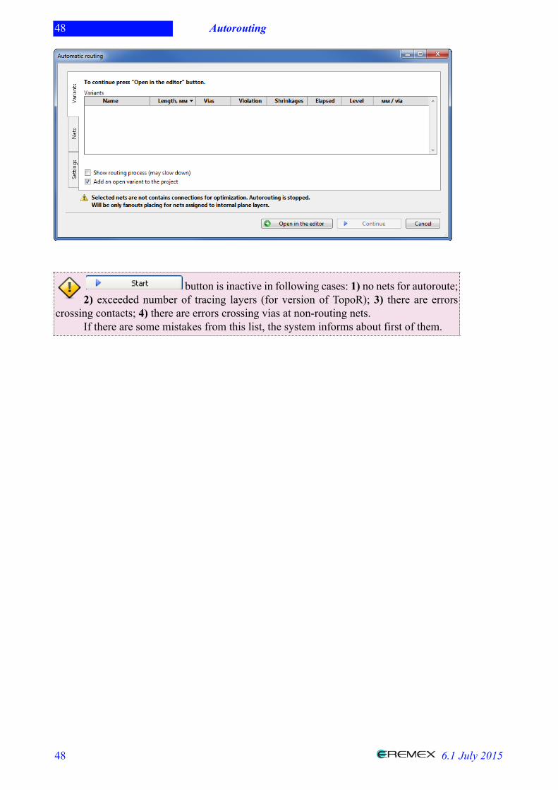
button is inactive in following cases: 1) no nets for autoroute;2) exceeded number of tracing layers (for version of TopoR); 3) there are errors
crossing contacts; 4) there are errors crossing vias at non-routing nets. If there are some mistakes from this list, the system informs about first of them.
49 Nets Tab
49 6.1 July 2015
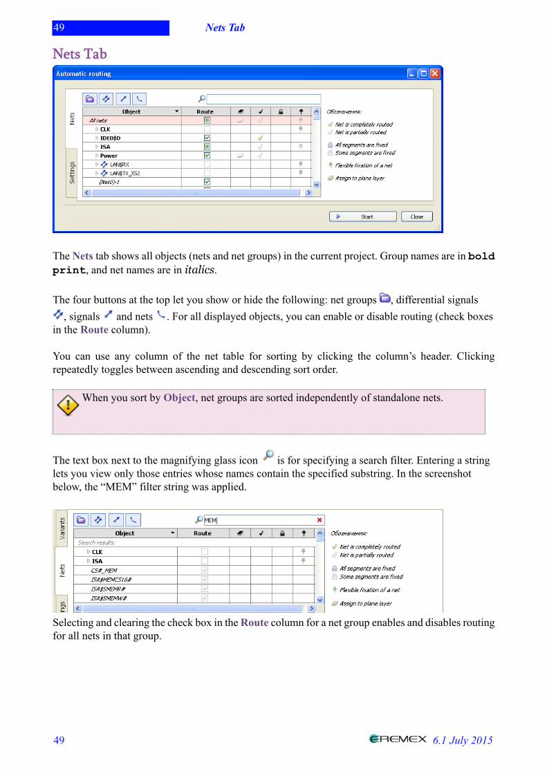
Nets Tab
The Nets tab shows all objects (nets and net groups) in the current project. Group names are in boldprint, and net names are in italics.
The four buttons at the top let you show or hide the following: net groups , differential signals , signals and nets . For all displayed objects, you can enable or disable routing (check boxes
in the Route column).
You can use any column of the net table for sorting by clicking the column’s header. Clickingrepeatedly toggles between ascending and descending sort order.
When you sort by Object, net groups are sorted independently of standalone nets.
The text box next to the magnifying glass icon is for specifying a search filter. Entering a stringlets you view only those entries whose names contain the specified substring. In the screenshotbelow, the “MEM” filter string was applied.
Selecting and clearing the check box in the Route column for a net group enables and disables routingfor all nets in that group.
50 Nets Tab
50 6.1 July 2015
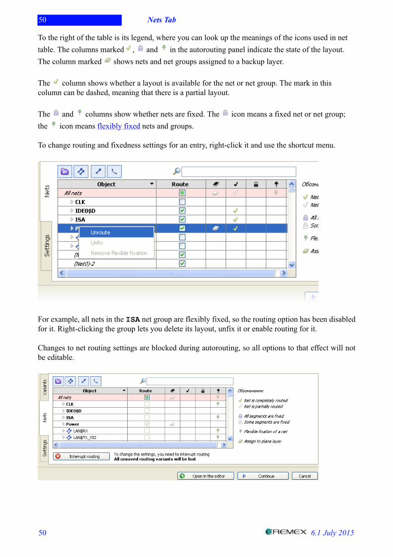
To the right of the table is its legend, where you can look up the meanings of the icons used in nettable. The columns marked , and in the autorouting panel indicate the state of the layout.The column marked shows nets and net groups assigned to a backup layer.
The column shows whether a layout is available for the net or net group. The mark in thiscolumn can be dashed, meaning that there is a partial layout.
The and columns show whether nets are fixed. The icon means a fixed net or net group;the icon means flexibly fixed nets and groups.
To change routing and fixedness settings for an entry, right-click it and use the shortcut menu.
For example, all nets in the ISA net group are flexibly fixed, so the routing option has been disabledfor it. Right-clicking the group lets you delete its layout, unfix it or enable routing for it.
Changes to net routing settings are blocked during autorouting, so all options to that effect will notbe editable.
51 Nets Tab
51 6.1 July 2015
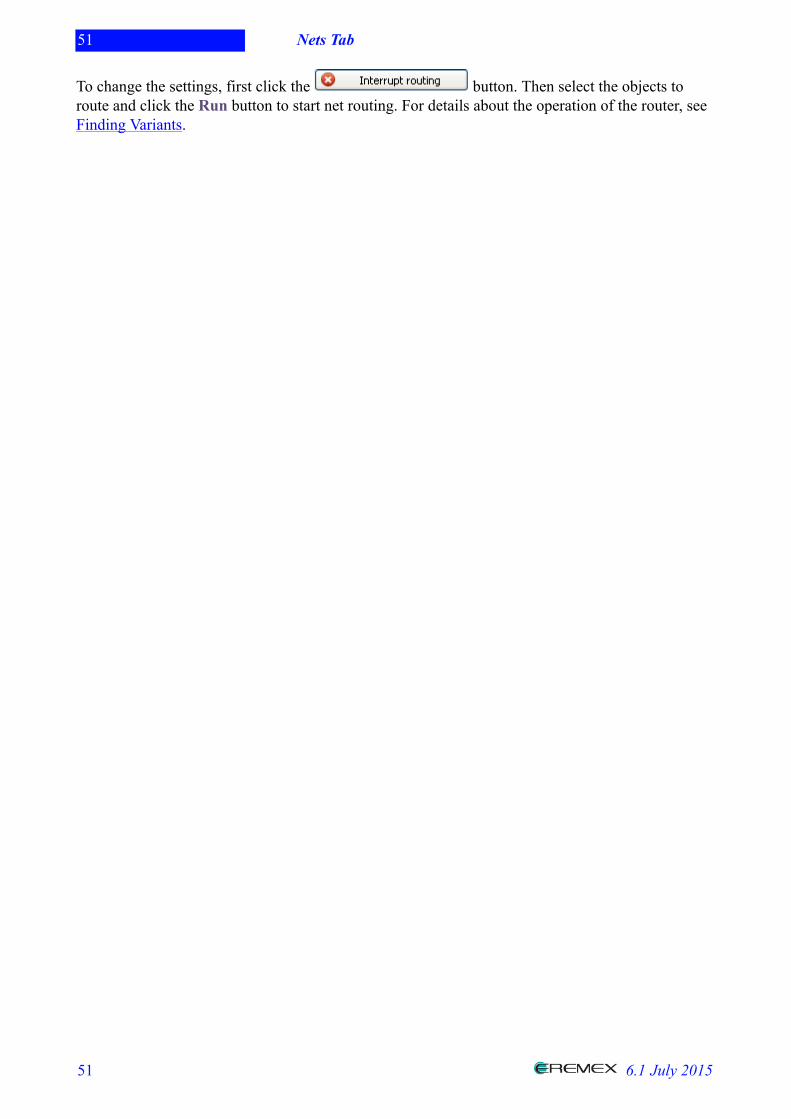
To change the settings, first click the button. Then select the objects toroute and click the Run button to start net routing. For details about the operation of the router, seeFinding Variants.
52 Settings Tab
52 6.1 July 2015
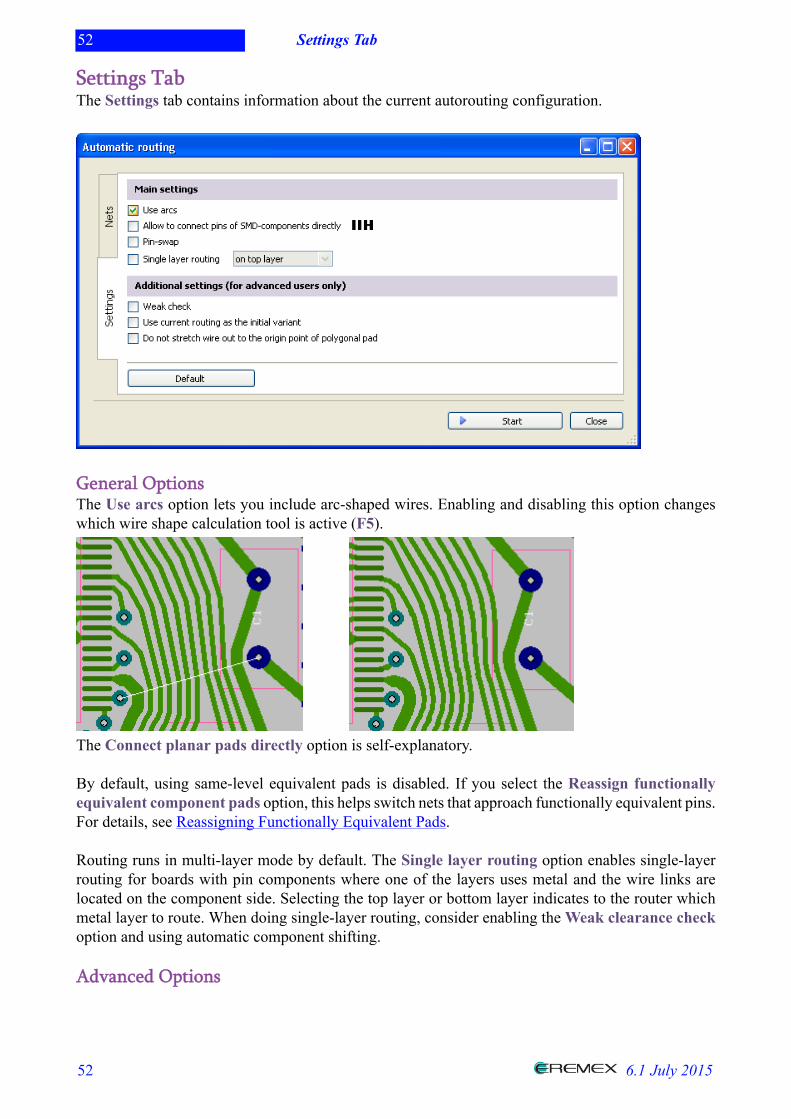
Settings TabThe Settings tab contains information about the current autorouting configuration.
General OptionsThe Use arcs option lets you include arc-shaped wires. Enabling and disabling this option changeswhich wire shape calculation tool is active (F5).
The Connect planar pads directly option is self-explanatory.
By default, using same-level equivalent pads is disabled. If you select the Reassign functionallyequivalent component pads option, this helps switch nets that approach functionally equivalent pins.For details, see Reassigning Functionally Equivalent Pads.
Routing runs in multi-layer mode by default. The Single layer routing option enables single-layerrouting for boards with pin components where one of the layers uses metal and the wire links arelocated on the component side. Selecting the top layer or bottom layer indicates to the router whichmetal layer to route. When doing single-layer routing, consider enabling the Weak clearance checkoption and using automatic component shifting.
Advanced Options
53 Settings Tab
53 6.1 July 2015
When the Weak clearance check option is enabled, the router is allowed to ignore violations thatmay occur between the pads of different (non-fixed) components. These violations are supposed tobe subsequently eliminated using the automatic component shifting procedure (F7).
This procedure must be started manually after a routing variant has been opened in the editor.
The Reuse existing layout as a starting point option lets you take advantage of the current layoutof the nets you are routing.
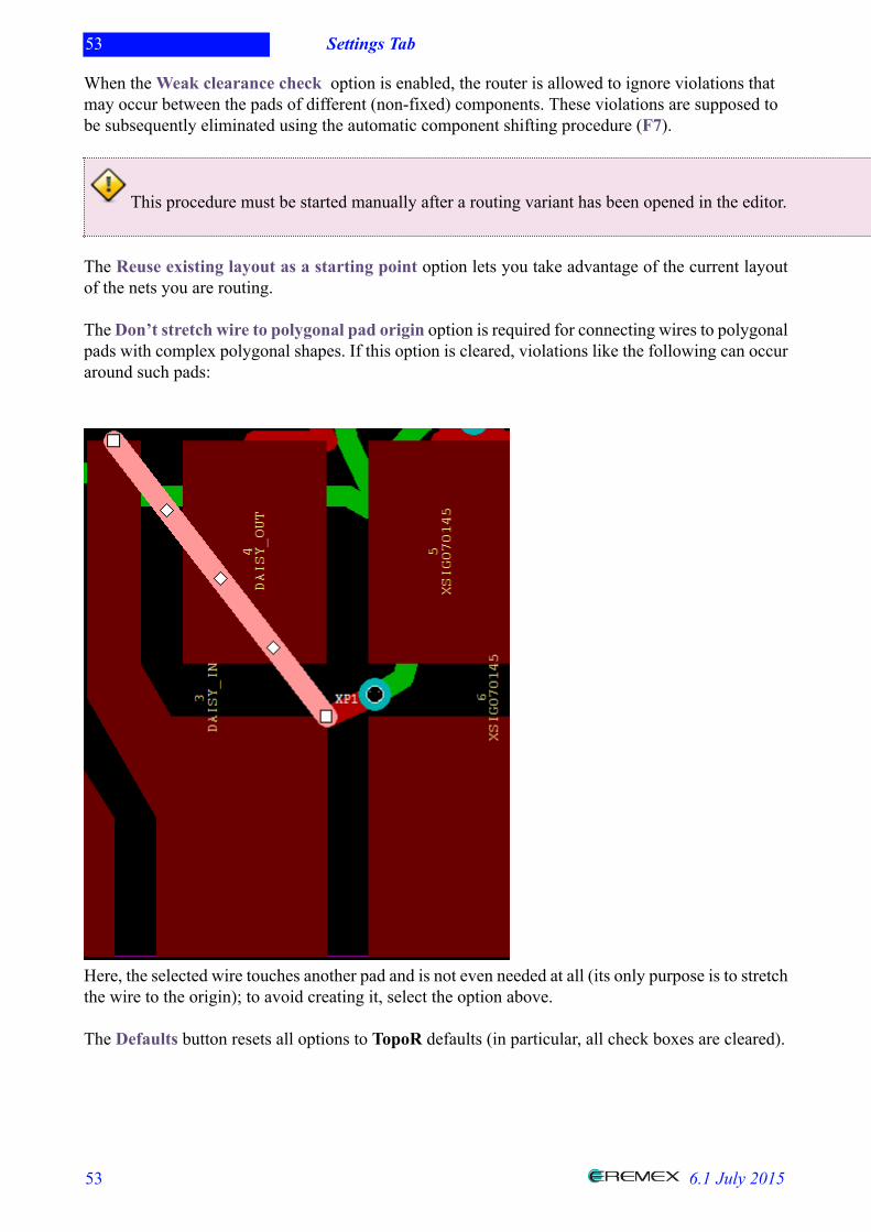
The Don’t stretch wire to polygonal pad origin option is required for connecting wires to polygonalpads with complex polygonal shapes. If this option is cleared, violations like the following can occuraround such pads:
Here, the selected wire touches another pad and is not even needed at all (its only purpose is to stretchthe wire to the origin); to avoid creating it, select the option above.
The Defaults button resets all options to TopoR defaults (in particular, all check boxes are cleared).
54 Finding Variants
54 6.1 July 2015
Finding VariantsClick Routing ► Delete Layout in the main menu to remove all wires before routing, including fixedwires. This is a way to perform routing from scratch.
After routing has been started, the Variants tab appears in the routing control panel.
TopoR automatically selects the best routing variants and saves them in the table using the followingnaming convention: name_LLL-VVV.fsb, where name is the board name, LLL is the total wirelength in millimeters, and VVV is the number of vias.
In addition to the estimated total wire length and number of vias, the .fsb file name containsinformation about the routing mode. Routing mode “w” means weak check, and “s” means strictcheck. If the file name contains the letter “a”, this means that arc-shaped wires were allowed duringrouting. The digits at the end of a file name (if any) do not have any meaning and are used just tomake the file name unique.
The variant name is shown in the table’s Name column, and each table row also includes the followingparameters of the variant:# Length is the total length of unsmoothed connections (usually exceeds the length of smoothed-out connections by 10 to 15 percent).# Vias is the number of vias.# Errors is the number of design constraint violations.# Shrinkages is the number of width reductions in nominally-wide wires.# Elapsed is the time it took to get the result.# Round is the number of the net shifting iteration that produced the variant (round 1 means thevery first iteration).# mm/via is the comparison between this variant and the previous best. By default, the currentvariant list is sorted by number of violations, then by ascending length. For the shortest variant, themm/via is usually empty, and for subsequent variants with as many violations and fewer vias thecolumn shows the length increase (in previously specified units) per removed via.
All of the table rows can be sorted by any parameter in ascending and descending order even as therouting is in progress.
55 Finding Variants
55 6.1 July 2015
During routing, variants can be added to the table and removed from it. The algorithm that controlsthis is quite complex. In most situations, the following rules apply:# A variant is removed (or rather, superseded by a new one) if the new variant is better on allparameters considered by the router (length, number of vias, number of violations, number ofshrinkages).# A variant is added if the new variant is at least as good as the best existing one on oneparameter or a combination of parameters.
When there have not been any improvements to the existing variants in a long time, the system showsthe Autorouting may be stopped message in the variant view.
Optimization Criteria in TopoRThe major quality criteria in the TopoR system are as follows:# Number of errors# Number of vias# Total length of connections# Number of shrinkages (wire width reductions in bottlenecks)
The system automatically stores variants with the best parameters. The first saved variant appears onlyafter the first optimization cycle has been completed or 20 seconds after the start of the optimization.Subsequently, saving occurs as the layout quality improves. The variants in which all parameters areworst will be removed automatically.
The optimization process can continue indefinitely until it is stopped manually using the Stop button. Do not stop the optimization process before the value in the Round column reaches 5–10.If TopoR keeps saving new versions, then it’s best not to stop it. When there have not been anyimprovements to the existing variants in a long time, the system shows a message that suggestsstopping the optimization.
To decide on the right moment to stop, you can also consider the changes in the ratio of total wirelength to the number of vias (the mm/via column). Practice shows that good results are achieved atthe ratio of 25mm/via (1000mil/via).
Selecting the Best VariantUnlike other systems, TopoR simultaneously optimizes multiple alternative variants of the layout,with different parameters optimized differently. You can select the layout configuration that suits youbest. Select those of the automatically saved variants that you find optimal, and add them to the project.
To add a variant from the table to the project, either right-click it and select Add to project, or clickthe + icon in variant entry.
56 Finding Variants
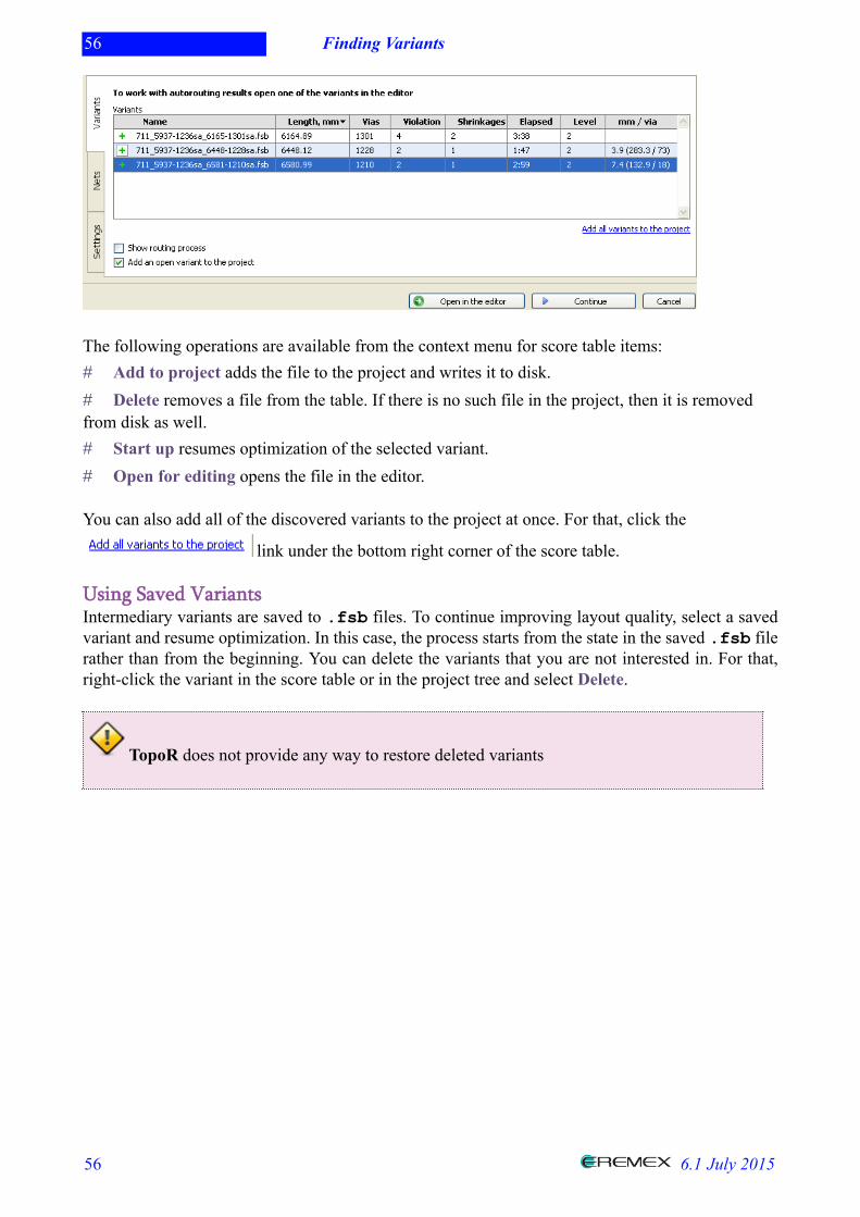
56 6.1 July 2015
The following operations are available from the context menu for score table items:# Add to project adds the file to the project and writes it to disk.# Delete removes a file from the table. If there is no such file in the project, then it is removedfrom disk as well.# Start up resumes optimization of the selected variant.# Open for editing opens the file in the editor.
You can also add all of the discovered variants to the project at once. For that, click the
link under the bottom right corner of the score table.
Using Saved VariantsIntermediary variants are saved to .fsb files. To continue improving layout quality, select a savedvariant and resume optimization. In this case, the process starts from the state in the saved .fsb filerather than from the beginning. You can delete the variants that you are not interested in. For that,right-click the variant in the score table or in the project tree and select Delete.
TopoR does not provide any way to restore deleted variants
57 Routing BGA Components
57 6.1 July 2015
Routing BGA Components
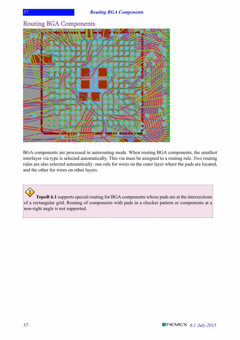
BGA components are processed in autorouting mode. When routing BGA components, the smallestinterlayer via type is selected automatically. This via must be assigned to a routing rule. Two routingrules are also selected automatically: one rule for wires on the outer layer where the pads are located,and the other for wires on other layers.
TopoR 6.1 supports special routing for BGA components whose pads are at the intersectionsof a rectangular grid. Routing of components with pads in a checker pattern or components at anon-right angle is not supported.
58 Conditional Routing
58 6.1 July 2015
Conditional RoutingTopoR 6.1 provides conditional routing of wires, meaning a special autorouting mode where theoptimal route is found only for a subset of the wires. To avoid deletion of the previous layout but keepit out of the way, consider flexible fixing of wires.
The procedure is generally as follows:1) Select the nets to route.2) Start routing.3) After routing has stopped, edit the result manually.4) If the resulting routes of the selected nets are acceptable, enable flexible fixing for these nets.5) If necessary, go to step 1.
Flexible fixing is intended for preserving the topology of a net without necessarily keeping itsgeometry (for example, a wire between two pads can be placed higher, lower or further to the rightor left than the original).
When the flexible fixing option is enabled, the routing control option is disabledautomatically.
The paths of flexibly fixed wires are not automatically optimized during automaticcomponent shifting (see Refine Tool).
If the results of autorouting are not quite acceptable, the routed nets should not be fixed (flexiblyor otherwise). In that case, you can enable the Resume routing from current configuration optionon the autorouting settings tab. As long as the option is disabled, all non-fixed routable nets will beautomatically deleted when autorouting starts.
59 Automatic placement
59 6.1 July 2015
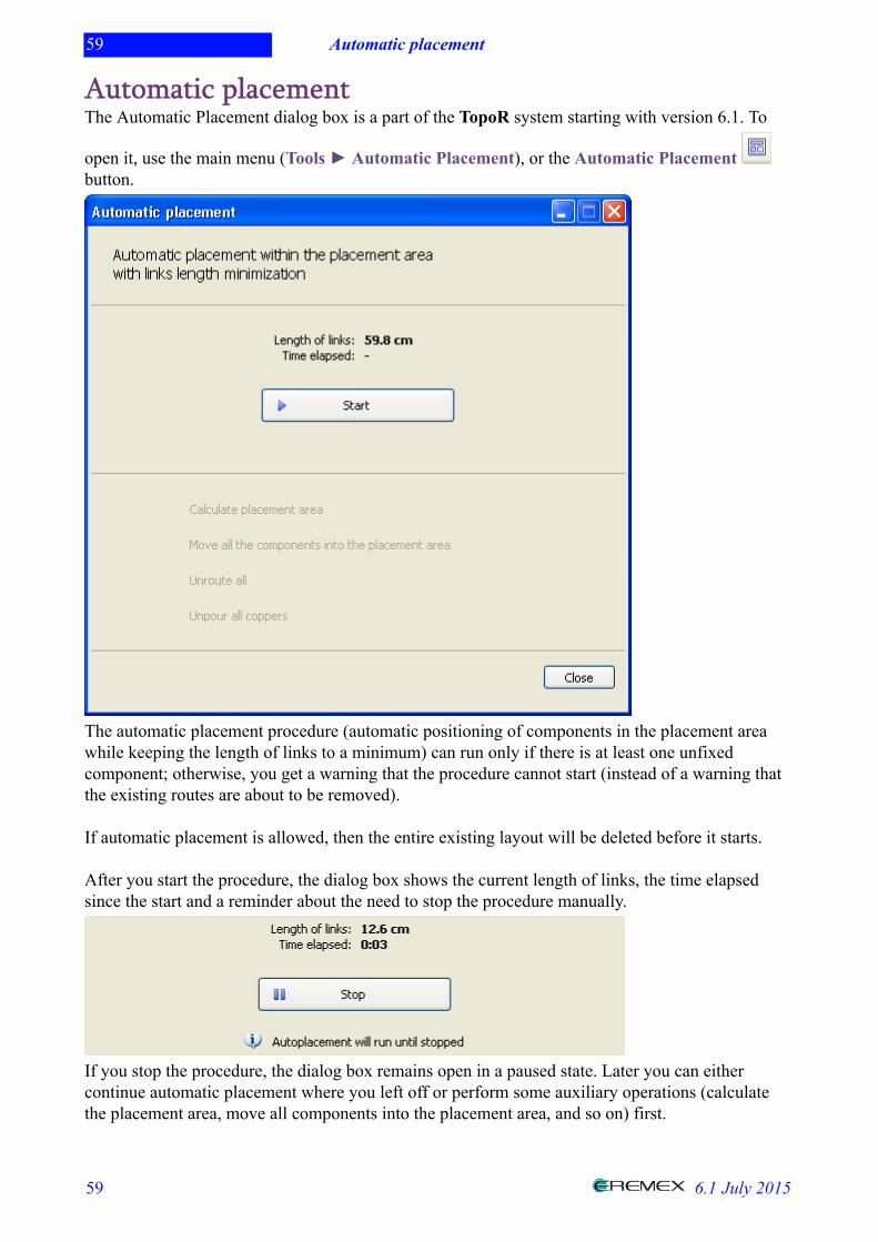
Automatic placementThe Automatic Placement dialog box is a part of the TopoR system starting with version 6.1. To
open it, use the main menu (Tools ► Automatic Placement), or the Automatic Placement button.
The automatic placement procedure (automatic positioning of components in the placement areawhile keeping the length of links to a minimum) can run only if there is at least one unfixedcomponent; otherwise, you get a warning that the procedure cannot start (instead of a warning thatthe existing routes are about to be removed). If automatic placement is allowed, then the entire existing layout will be deleted before it starts. After you start the procedure, the dialog box shows the current length of links, the time elapsedsince the start and a reminder about the need to stop the procedure manually.
If you stop the procedure, the dialog box remains open in a paused state. Later you can eithercontinue automatic placement where you left off or perform some auxiliary operations (calculatethe placement area, move all components into the placement area, and so on) first.
60 Automatic placement
60 6.1 July 2015
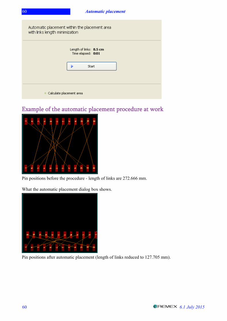
Example of the automatic placement procedure at work
Pin positions before the procedure - length of links are 272.666 mm. What the automatic placement dialog box shows.
Pin positions after automatic placement (length of links reduced to 127.705 mm).
61 Automatic placement
61 6.1 July 2015
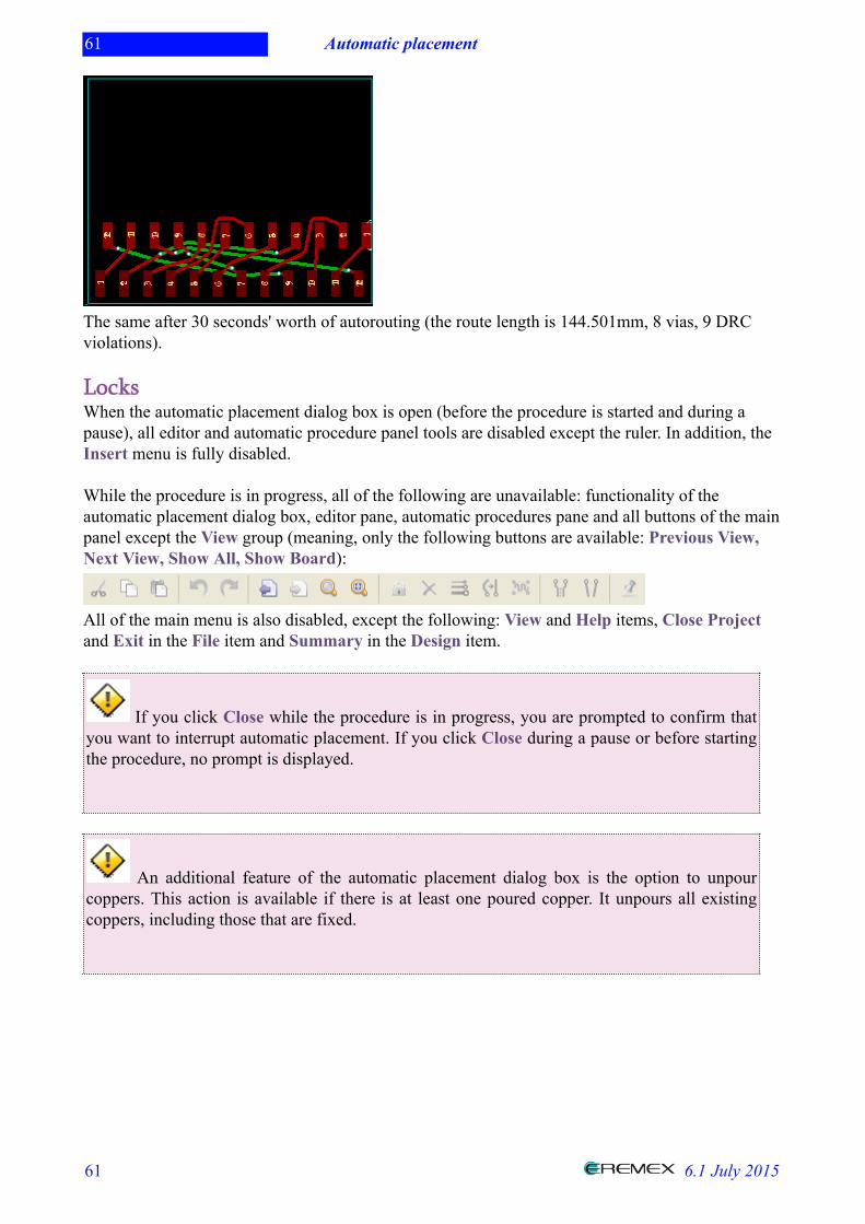
The same after 30 seconds' worth of autorouting (the route length is 144.501mm, 8 vias, 9 DRCviolations). LocksWhen the automatic placement dialog box is open (before the procedure is started and during apause), all editor and automatic procedure panel tools are disabled except the ruler. In addition, theInsert menu is fully disabled. While the procedure is in progress, all of the following are unavailable: functionality of theautomatic placement dialog box, editor pane, automatic procedures pane and all buttons of the mainpanel except the View group (meaning, only the following buttons are available: Previous View,Next View, Show All, Show Board):
All of the main menu is also disabled, except the following: View and Help items, Close Projectand Exit in the File item and Summary in the Design item.
If you click Close while the procedure is in progress, you are prompted to confirm thatyou want to interrupt automatic placement. If you click Close during a pause or before startingthe procedure, no prompt is displayed.
An additional feature of the automatic placement dialog box is the option to unpourcoppers. This action is available if there is at least one poured copper. It unpours all existingcoppers, including those that are fixed.
62 TopoR Editor Tools
62 6.1 July 2015
TopoR Editor ToolsThis section describes the main menu of the program, the toolbar, the action bar, the selection filter,the visibility pane, the search pane and the context menus.
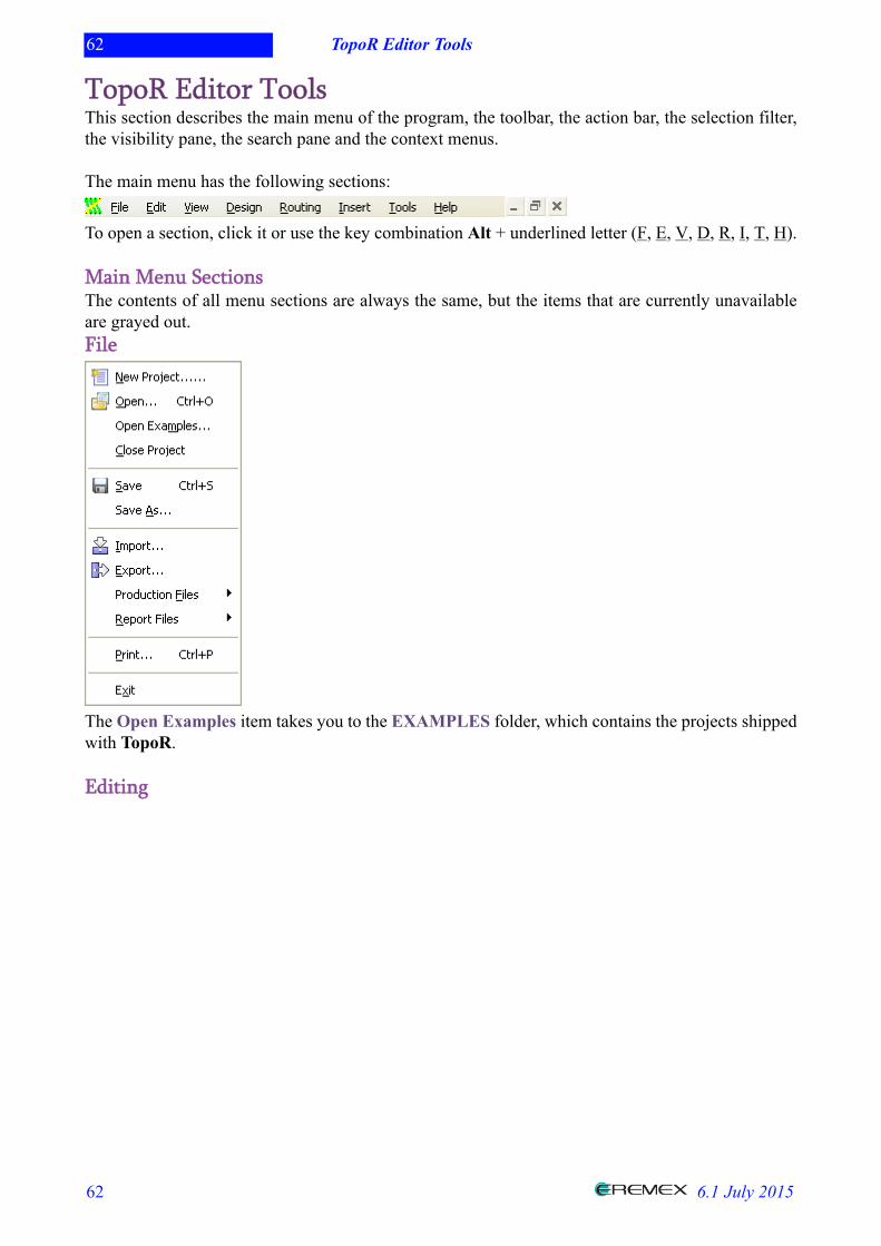
The main menu has the following sections:
To open a section, click it or use the key combination Alt + underlined letter (F, E, V, D, R, I, T, H).
Main Menu SectionsThe contents of all menu sections are always the same, but the items that are currently unavailableare grayed out.File
The Open Examples item takes you to the EXAMPLES folder, which contains the projects shippedwith TopoR.
Editing
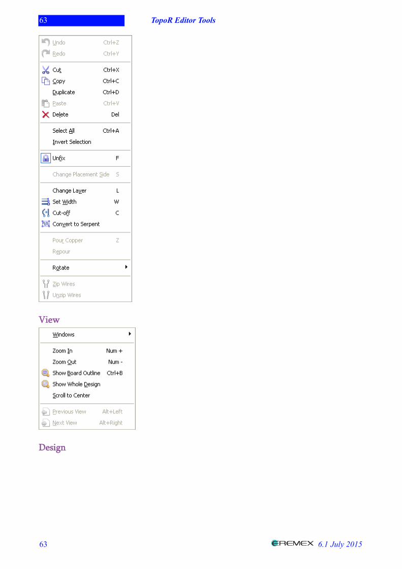
63 TopoR Editor Tools
63 6.1 July 2015
View
Design
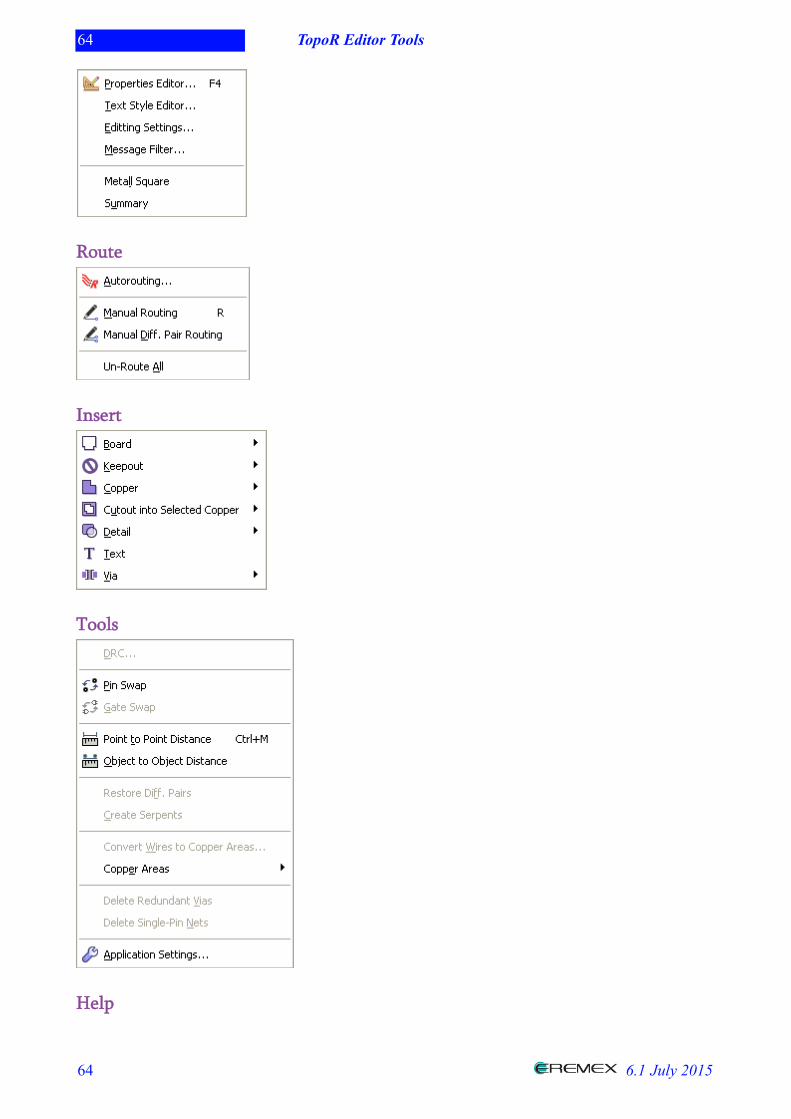
64 TopoR Editor Tools
64 6.1 July 2015
Route
Insert
Tools
Help
65 TopoR Editor Tools
65 6.1 July 2015
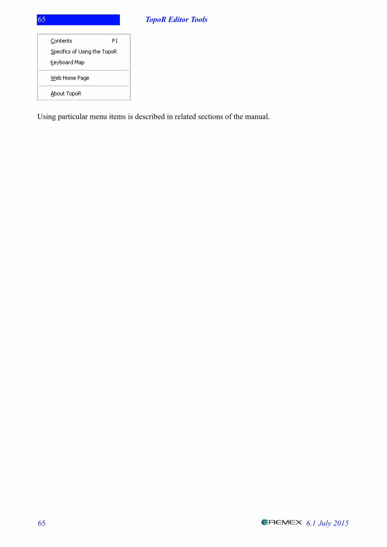
Using particular menu items is described in related sections of the manual.
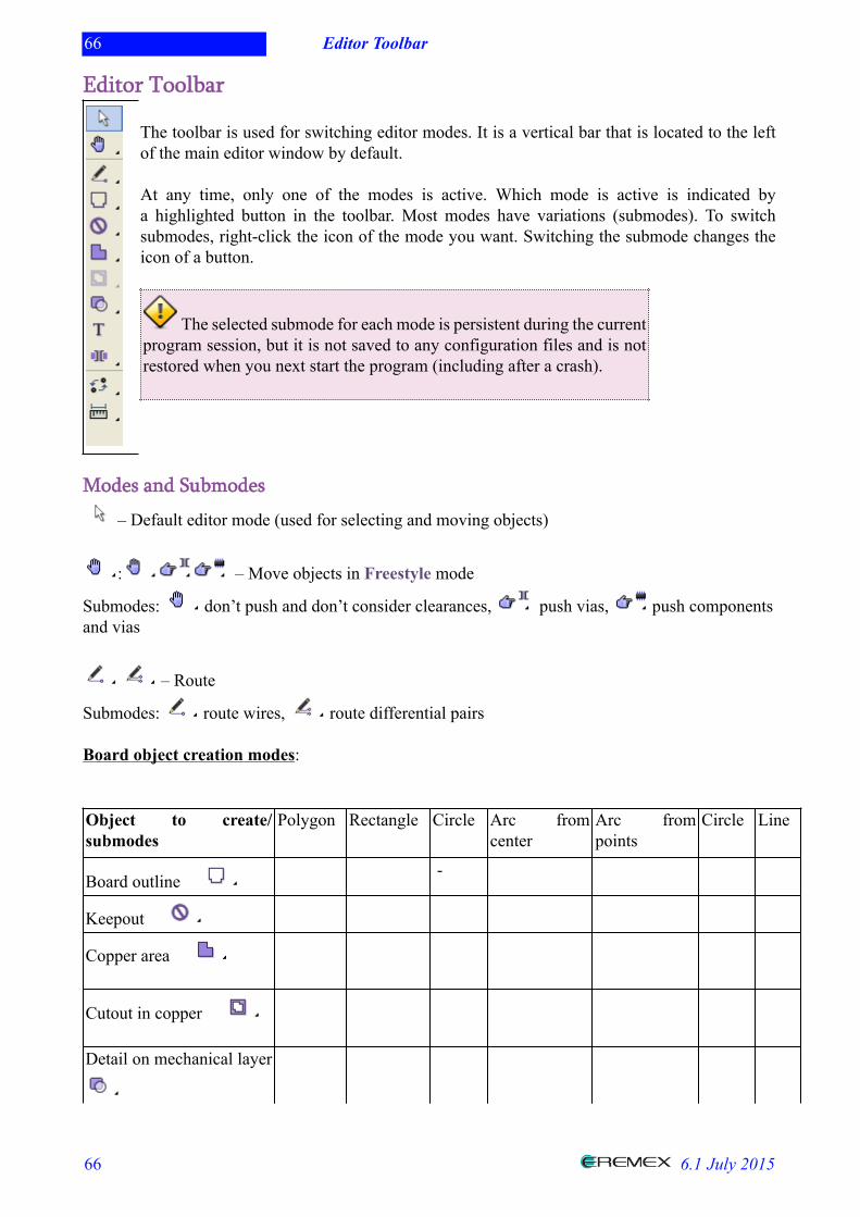
66 Editor Toolbar
66 6.1 July 2015
Editor Toolbar
The toolbar is used for switching editor modes. It is a vertical bar that is located to the leftof the main editor window by default.
At any time, only one of the modes is active. Which mode is active is indicated bya highlighted button in the toolbar. Most modes have variations (submodes). To switchsubmodes, right-click the icon of the mode you want. Switching the submode changes theicon of a button.
The selected submode for each mode is persistent during the currentprogram session, but it is not saved to any configuration files and is notrestored when you next start the program (including after a crash).
Modes and Submodes
– Default editor mode (used for selecting and moving objects)
: – Move objects in Freestyle mode
Submodes: don’t push and don’t consider clearances, push vias, push componentsand vias
– Route
Submodes: route wires, route differential pairs
Board object creation modes: Object to create/submodes
Polygon Rectangle Circle Arc fromcenter
Arc frompoints
Circle Line
Board outline -
Keepout
Copper area
Cutout in copper
Detail on mechanical layer
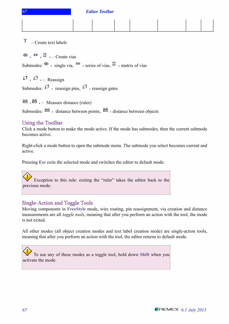
67 Editor Toolbar
67 6.1 July 2015
– Create text labels
– Create vias
Submodes: single via, series of vias, matrix of vias
– Reassign
Submodes: reassign pins, reassign gates
– Measure distance (ruler)
Submodes: distance between points, distance between objects
Using the ToolbarClick a mode button to make the mode active. If the mode has submodes, then the current submodebecomes active.
Right-click a mode button to open the submode menu. The submode you select becomes current andactive.
Pressing Esc exits the selected mode and switches the editor to default mode.
Exception to this rule: exiting the “ruler” takes the editor back to theprevious mode.
Single-Action and Toggle ToolsMoving components in FreeStyle mode, wire routing, pin reassignment, via creation and distancemeasurements are all toggle tools, meaning that after you perform an action with the tool, the modeis not exited.
All other modes (all object creation modes and text label creation mode) are single-action tools,meaning that after you perform an action with the tool, the editor returns to default mode.
To use any of these modes as a toggle tool, hold down Shift when youactivate the mode.
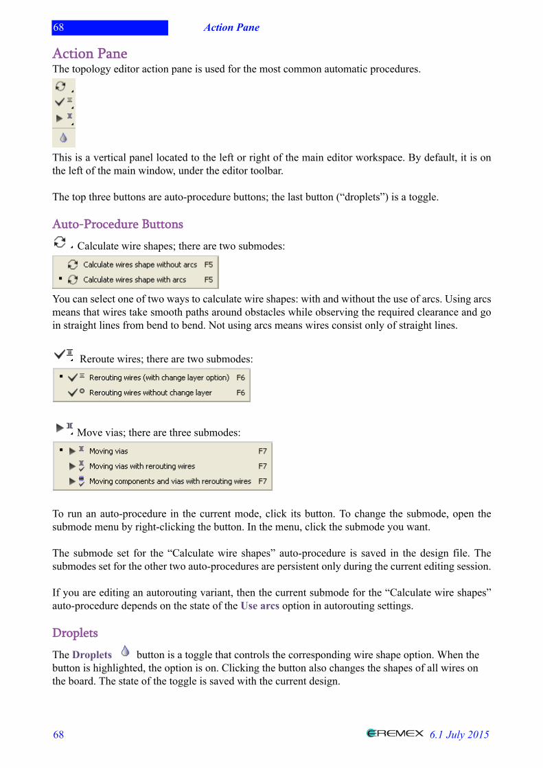
68 Action Pane
68 6.1 July 2015
Action PaneThe topology editor action pane is used for the most common automatic procedures.
This is a vertical panel located to the left or right of the main editor workspace. By default, it is onthe left of the main window, under the editor toolbar.
The top three buttons are auto-procedure buttons; the last button (“droplets”) is a toggle.
Auto-Procedure Buttons
Calculate wire shapes; there are two submodes:
You can select one of two ways to calculate wire shapes: with and without the use of arcs. Using arcsmeans that wires take smooth paths around obstacles while observing the required clearance and goin straight lines from bend to bend. Not using arcs means wires consist only of straight lines.
Reroute wires; there are two submodes:
Move vias; there are three submodes:
To run an auto-procedure in the current mode, click its button. To change the submode, open thesubmode menu by right-clicking the button. In the menu, click the submode you want.
The submode set for the “Calculate wire shapes” auto-procedure is saved in the design file. Thesubmodes set for the other two auto-procedures are persistent only during the current editing session.
If you are editing an autorouting variant, then the current submode for the “Calculate wire shapes”auto-procedure depends on the state of the Use arcs option in autorouting settings.
Droplets
The Droplets button is a toggle that controls the corresponding wire shape option. When thebutton is highlighted, the option is on. Clicking the button also changes the shapes of all wires onthe board. The state of the toggle is saved with the current design.
69 Selection Filter
69 6.1 July 2015
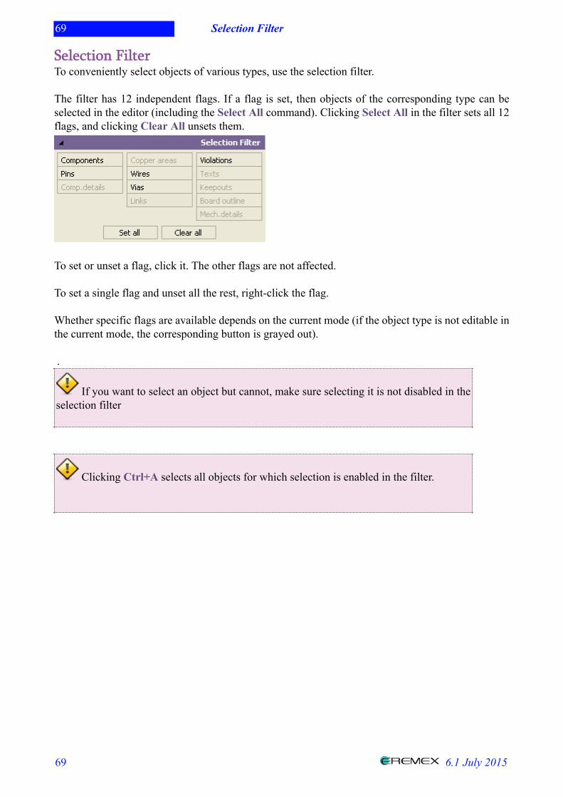
Selection FilterTo conveniently select objects of various types, use the selection filter.
The filter has 12 independent flags. If a flag is set, then objects of the corresponding type can beselected in the editor (including the Select All command). Clicking Select All in the filter sets all 12flags, and clicking Clear All unsets them.
To set or unset a flag, click it. The other flags are not affected.
To set a single flag and unset all the rest, right-click the flag.
Whether specific flags are available depends on the current mode (if the object type is not editable inthe current mode, the corresponding button is grayed out). .
If you want to select an object but cannot, make sure selecting it is not disabled in theselection filter
Clicking Ctrl+A selects all objects for which selection is enabled in the filter.
70 Context Menus
70 6.1 July 2015
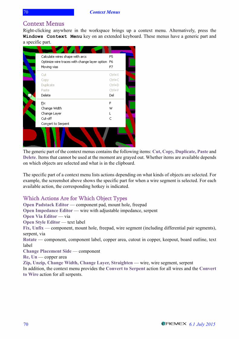
Context MenusRight-clicking anywhere in the workspace brings up a context menu. Alternatively, press theWindows Context Menu key on an extended keyboard. These menus have a generic part anda specific part.
The generic part of the context menus contains the following items: Cut, Copy, Duplicate, Paste andDelete. Items that cannot be used at the moment are grayed out. Whether items are available dependson which objects are selected and what is in the clipboard.
The specific part of a context menu lists actions depending on what kinds of objects are selected. Forexample, the screenshot above shows the specific part for when a wire segment is selected. For eachavailable action, the corresponding hotkey is indicated.
Which Actions Are for Which Object TypesOpen Padstack Editor — component pad, mount hole, freepadOpen Impedance Editor — wire with adjustable impedance, serpentOpen Via Editor — viaOpen Style Editor — text labelFix, Unfix — component, mount hole, freepad, wire segment (including differential pair segments),serpent, viaRotate — component, component label, copper area, cutout in copper, keepout, board outline, textlabelChange Placement Side — componentRe, Un — copper areaZip, Unzip, Change Width, Change Layer, Straighten — wire, wire segment, serpentIn addition, the context menu provides the Convert to Serpent action for all wires and the Convertto Wire action for all serpents.
71 Display Control
71 6.1 July 2015
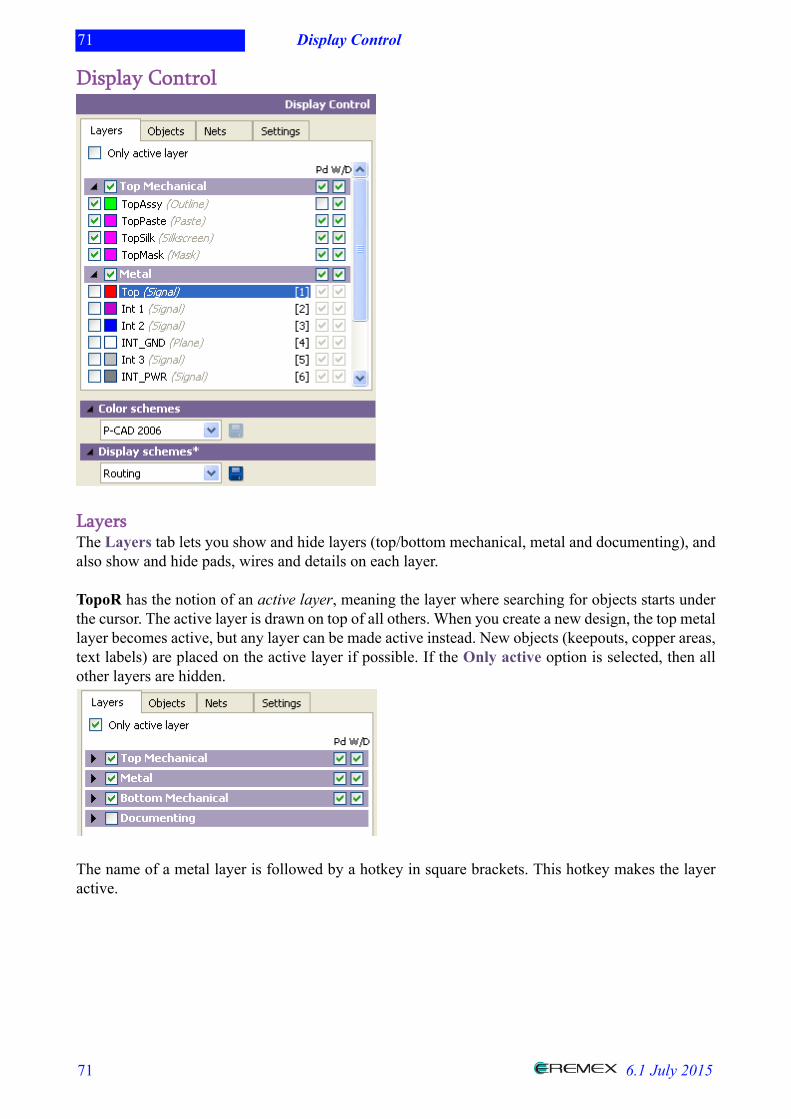
Display Control
LayersThe Layers tab lets you show and hide layers (top/bottom mechanical, metal and documenting), andalso show and hide pads, wires and details on each layer.
TopoR has the notion of an active layer, meaning the layer where searching for objects starts underthe cursor. The active layer is drawn on top of all others. When you create a new design, the top metallayer becomes active, but any layer can be made active instead. New objects (keepouts, copper areas,text labels) are placed on the active layer if possible. If the Only active option is selected, then allother layers are hidden.
The name of a metal layer is followed by a hotkey in square brackets. This hotkey makes the layeractive.
72 Display Control
72 6.1 July 2015
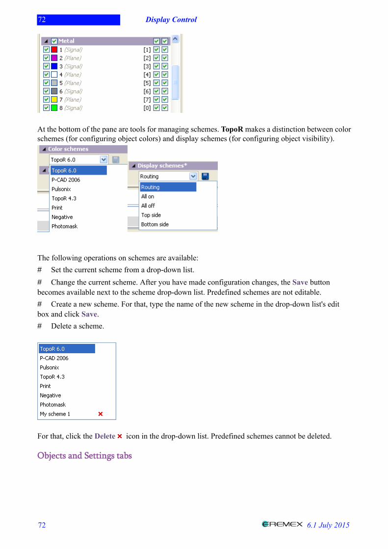
At the bottom of the pane are tools for managing schemes. TopoR makes a distinction between colorschemes (for configuring object colors) and display schemes (for configuring object visibility).
The following operations on schemes are available:# Set the current scheme from a drop-down list.# Change the current scheme. After you have made configuration changes, the Save buttonbecomes available next to the scheme drop-down list. Predefined schemes are not editable.# Create a new scheme. For that, type the name of the new scheme in the drop-down list's editbox and click Save.# Delete a scheme.
For that, click the Delete icon in the drop-down list. Predefined schemes cannot be deleted.
Objects and Settings tabs
73 Display Control
73 6.1 July 2015
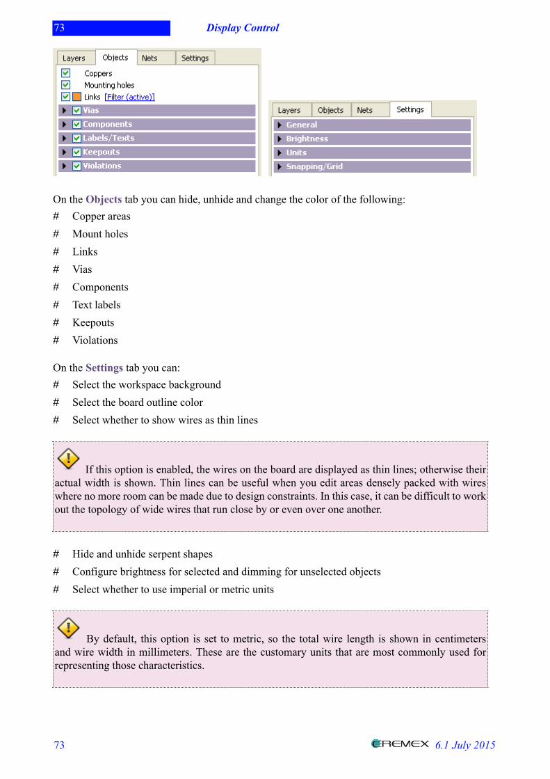
On the Objects tab you can hide, unhide and change the color of the following:# Copper areas# Mount holes# Links# Vias# Components# Text labels# Keepouts# Violations
On the Settings tab you can:# Select the workspace background# Select the board outline color# Select whether to show wires as thin lines
If this option is enabled, the wires on the board are displayed as thin lines; otherwise theiractual width is shown. Thin lines can be useful when you edit areas densely packed with wireswhere no more room can be made due to design constraints. In this case, it can be difficult to workout the topology of wide wires that run close by or even over one another.
# Hide and unhide serpent shapes# Configure brightness for selected and dimming for unselected objects# Select whether to use imperial or metric units
By default, this option is set to metric, so the total wire length is shown in centimetersand wire width in millimeters. These are the customary units that are most commonly used forrepresenting those characteristics.
74 Display Control
74 6.1 July 2015
# Enable or disable angle snapping# Specify the type (points or lines), color and horizontal and vertical step for the grid Nets
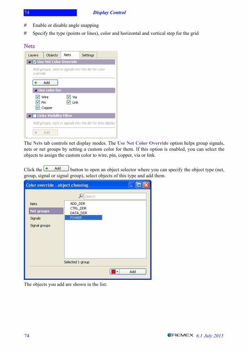
The Nets tab controls net display modes. The Use Net Color Override option helps group signals,nets or net groups by setting a custom color for them. If this option is enabled, you can select theobjects to assign the custom color to wire, pin, copper, via or link.
Click the button to open an object selector where you can specify the object type (net,group, signal or signal group), select objects of this type and add them.
The objects you add are shown in the list:
75 Display Control
75 6.1 July 2015
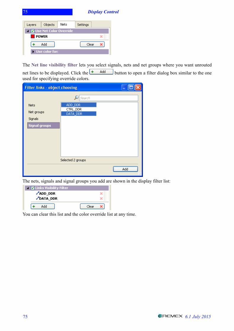
The Net line visibility filter lets you select signals, nets and net groups where you want unrouted
net lines to be displayed. Click the button to open a filter dialog box similar to the oneused for specifying override colors.
The nets, signals and signal groups you add are shown in the display filter list:
You can clear this list and the color override list at any time.
76 Search Panel
76 6.1 July 2015
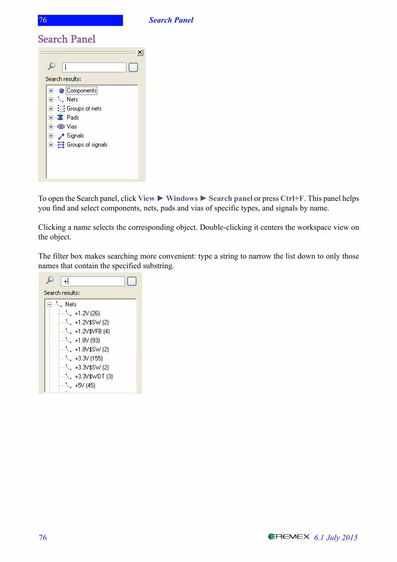
Search Panel
To open the Search panel, click View ► Windows ► Search panel or press Ctrl+F. This panel helpsyou find and select components, nets, pads and vias of specific types, and signals by name.
Clicking a name selects the corresponding object. Double-clicking it centers the workspace view onthe object.
The filter box makes searching more convenient: type a string to narrow the list down to only thosenames that contain the specified substring.
77 Ruler Tool
77 6.1 July 2015
Ruler ToolThe ruler is used for measuring distances on the board. You can activate it from the menu (mode 1: Tools ► Point to Point Distance or Ctrl+M, mode 2: Tools ► Object to Object Distance).
You can also activate it from the editor toolbar (one of the two submodes is enabled, and you canchange the submode by right-clicking the ruler icon ( or ):
The ruler is also enabled with the Ctrl+M hotkey. This activates the ruler in the submode that iscurrently selected on the toolbar.
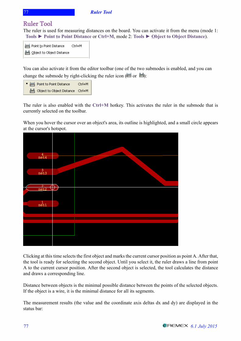
When you hover the cursor over an object's area, its outline is highlighted, and a small circle appearsat the cursor's hotspot.
Clicking at this time selects the first object and marks the current cursor position as point A. After that,the tool is ready for selecting the second object. Until you select it, the ruler draws a line from pointA to the current cursor position. After the second object is selected, the tool calculates the distanceand draws a corresponding line.
Distance between objects is the minimal possible distance between the points of the selected objects.If the object is a wire, it is the minimal distance for all its segments.
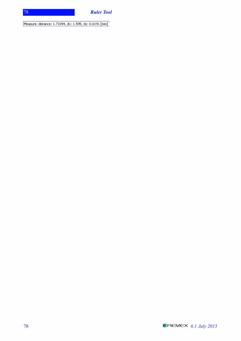
The measurement results (the value and the coordinate axis deltas dx and dy) are displayed in thestatus bar:
78 Ruler Tool
78 6.1 July 2015
79 Editor Settings
79 6.1 July 2015
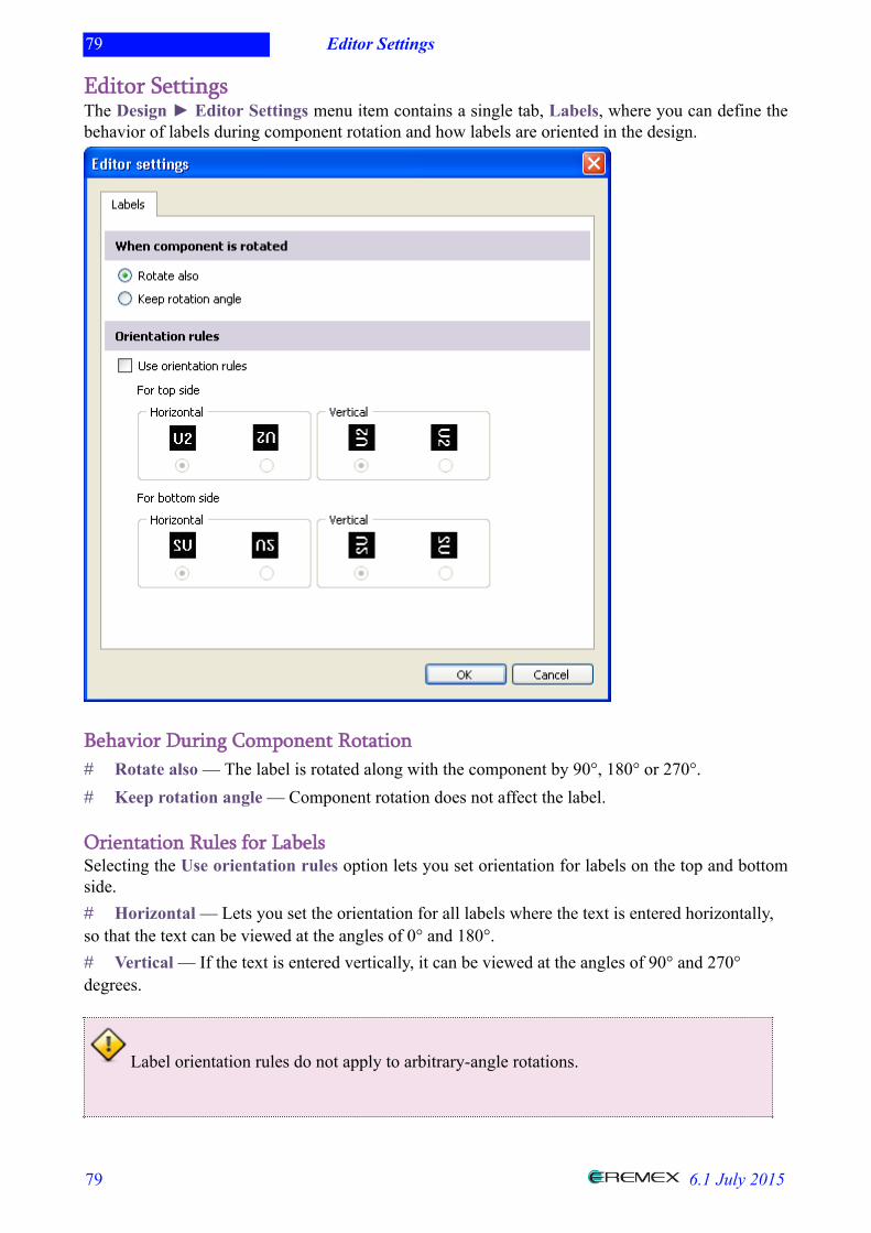
Editor SettingsThe Design ► Editor Settings menu item contains a single tab, Labels, where you can define thebehavior of labels during component rotation and how labels are oriented in the design.
Behavior During Component Rotation# Rotate also — The label is rotated along with the component by 90°, 180° or 270°.# Keep rotation angle — Component rotation does not affect the label.
Orientation Rules for LabelsSelecting the Use orientation rules option lets you set orientation for labels on the top and bottomside.# Horizontal — Lets you set the orientation for all labels where the text is entered horizontally,so that the text can be viewed at the angles of 0° and 180°.# Vertical — If the text is entered vertically, it can be viewed at the angles of 90° and 270°degrees.
Label orientation rules do not apply to arbitrary-angle rotations.

80 Editor Settings
80 6.1 July 2015

81 Manual Editing
81 6.1 July 2015
Manual EditingAs noted above, TopoR is not only routing software but also an efficient topology editor. This sectiondescribes editing tools available in TopoR.
82 Component Operations
82 6.1 July 2015
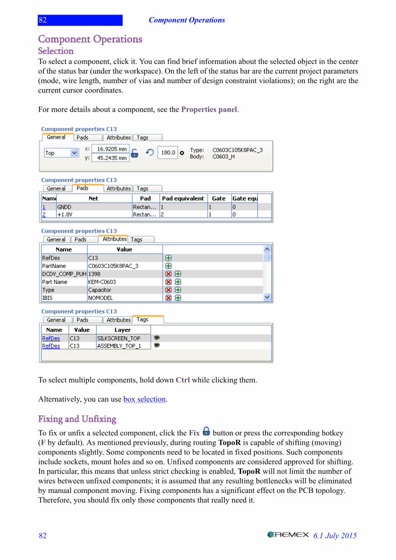
Component OperationsSelectionTo select a component, click it. You can find brief information about the selected object in the centerof the status bar (under the workspace). On the left of the status bar are the current project parameters(mode, wire length, number of vias and number of design constraint violations); on the right are thecurrent cursor coordinates.
For more details about a component, see the Properties panel.
To select multiple components, hold down Ctrl while clicking them.
Alternatively, you can use box selection.
Fixing and UnfixingTo fix or unfix a selected component, click the Fix button or press the corresponding hotkey(F by default). As mentioned previously, during routing TopoR is capable of shifting (moving)components slightly. Some components need to be located in fixed positions. Such componentsinclude sockets, mount holes and so on. Unfixed components are considered approved for shifting.In particular, this means that unless strict checking is enabled, TopoR will not limit the number ofwires between unfixed components; it is assumed that any resulting bottlenecks will be eliminatedby manual component moving. Fixing components has a significant effect on the PCB topology.Therefore, you should fix only those components that really need it.
83 Component Operations
83 6.1 July 2015
Changing SidesTo change the placement side for a component, click Edit ► Change Component Side in the mainmenu.
RotationsTo rotate components, use context menus, where the Rotate item has the following secondary items: Rotate by 90°, Rotate by -90° and Rotate by Angle. The first two commands have associatedhotkeys. You can do the same by clicking Edit ► Rotate in the main menu.
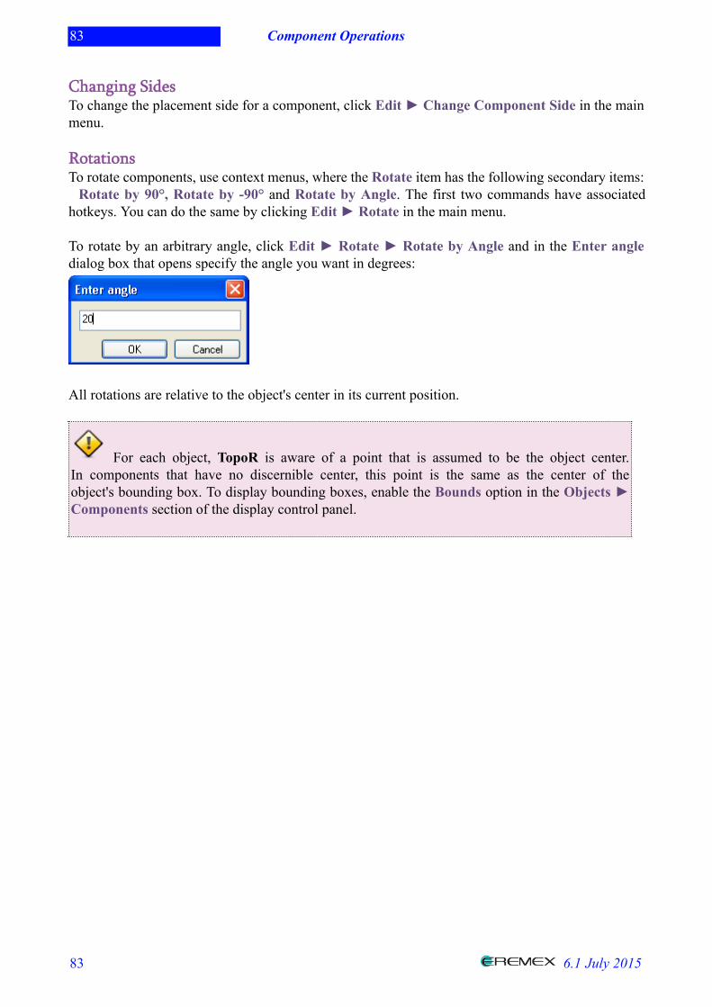
To rotate by an arbitrary angle, click Edit ► Rotate ► Rotate by Angle and in the Enter angledialog box that opens specify the angle you want in degrees:
All rotations are relative to the object's center in its current position.
For each object, TopoR is aware of a point that is assumed to be the object center.In components that have no discernible center, this point is the same as the center of theobject's bounding box. To display bounding boxes, enable the Bounds option in the Objects ►Components section of the display control panel.
84 Working with Component Attributes and Labels
84 6.1 July 2015
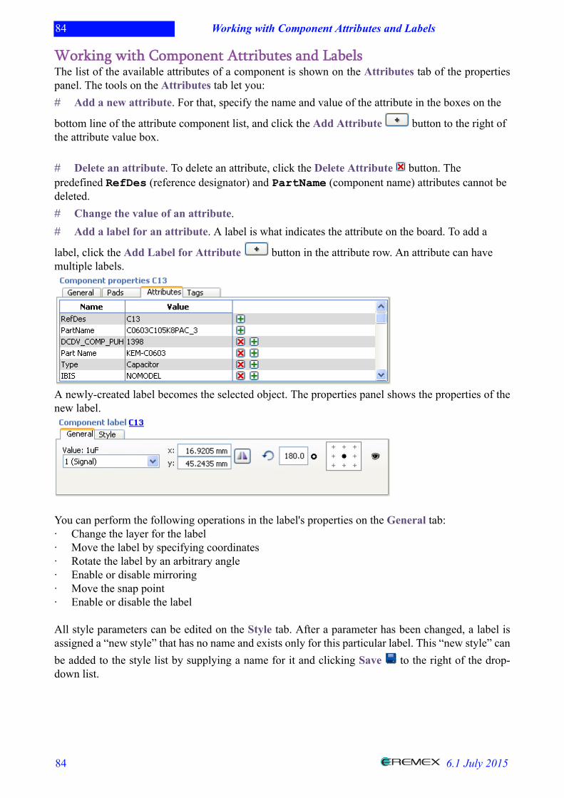
Working with Component Attributes and LabelsThe list of the available attributes of a component is shown on the Attributes tab of the propertiespanel. The tools on the Attributes tab let you:# Add a new attribute. For that, specify the name and value of the attribute in the boxes on the
bottom line of the attribute component list, and click the Add Attribute button to the right ofthe attribute value box. # Delete an attribute. To delete an attribute, click the Delete Attribute button. Thepredefined RefDes (reference designator) and PartName (component name) attributes cannot bedeleted.# Change the value of an attribute.# Add a label for an attribute. A label is what indicates the attribute on the board. To add a
label, click the Add Label for Attribute button in the attribute row. An attribute can havemultiple labels.
A newly-created label becomes the selected object. The properties panel shows the properties of thenew label.
You can perform the following operations in the label's properties on the General tab:· Change the layer for the label· Move the label by specifying coordinates· Rotate the label by an arbitrary angle· Enable or disable mirroring· Move the snap point· Enable or disable the label
All style parameters can be edited on the Style tab. After a parameter has been changed, a label isassigned a “new style” that has no name and exists only for this particular label. This “new style” canbe added to the style list by supplying a name for it and clicking Save to the right of the drop-down list.
85 Working with Component Attributes and Labels
85 6.1 July 2015
To disable a label, click the On/Off button on the General tab. A disabled label is not displayedor written to any exported files. To enable a label, use the same button again in the label propertiesor on the Labels tab in the component properties.
86 Operations on Wires
86 6.1 July 2015
Operations on WiresRouting
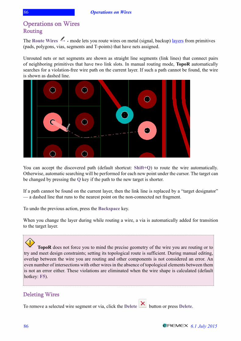
The Route Wires mode lets you route wires on metal (signal, backup) layers from primitives(pads, polygons, vias, segments and T-points) that have nets assigned.
Unrouted nets or net segments are shown as straight line segments (link lines) that connect pairsof neighboring primitives that have two link slots. In manual routing mode, TopoR automaticallysearches for a violation-free wire path on the current layer. If such a path cannot be found, the wireis shown as dashed line.
You can accept the discovered path (default shortcut: Shift+Q) to route the wire automatically.Otherwise, automatic searching will be performed for each new point under the cursor. The target canbe changed by pressing the Q key if the path to the new target is shorter.
If a path cannot be found on the current layer, then the link line is replaced by a “target designator”— a dashed line that runs to the nearest point on the non-connected net fragment.
To undo the previous action, press the Backspace key.
When you change the layer during while routing a wire, a via is automatically added for transitionto the target layer.
TopoR does not force you to mind the precise geometry of the wire you are routing or totry and meet design constraints; setting its topological route is sufficient. During manual editing,overlap between the wire you are routing and other components is not considered an error. Aneven number of intersections with other wires in the absence of topological elements between themis not an error either. These violations are eliminated when the wire shape is calculated (defaulthotkey: F5).
Deleting Wires
To remove a selected wire segment or via, click the Delete button or press Delete.
87 Operations on Wires
87 6.1 July 2015
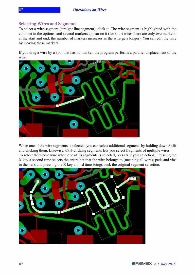
Selecting Wires and SegmentsTo select a wire segment (straight line segment), click it. The wire segment is highlighted with thecolor set in the options, and several markers appear on it (for short wires there are only two markers:at the start and end; the number of markers increases as the wire gets longer). You can edit the wireby moving these markers.
If you drag a wire by a spot that has no marker, the program performs a parallel displacement of thewire.
When one of the wire segments is selected, you can select additional segments by holding down Shiftand clicking them. Likewise, Ctrl-clicking segments lets you select fragments of multiple wires.To select the whole wire when one of its segments is selected, press X (cycle selection). Pressing theX key a second time selects the entire net that the wire belongs to (meaning all wires, pads and viasin the net), and pressing the X key a third time brings back the original segment selection.
88 Operations on Wires
88 6.1 July 2015
Straightening Wires
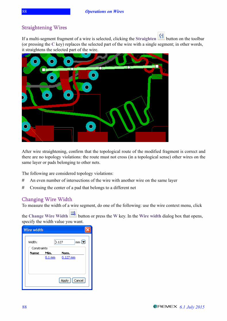
If a multi-segment fragment of a wire is selected, clicking the Straighten button on the toolbar(or pressing the C key) replaces the selected part of the wire with a single segment; in other words,it straightens the selected part of the wire.
After wire straightening, confirm that the topological route of the modified fragment is correct andthere are no topology violations: the route must not cross (in a topological sense) other wires on thesame layer or pads belonging to other nets.
The following are considered topology violations:# An even number of intersections of the wire with another wire on the same layer# Crossing the center of a pad that belongs to a different net
Changing Wire WidthTo measure the width of a wire segment, do one of the following: use the wire context menu, click
the Change Wire Width button or press the W key. In the Wire width dialog box that opens,specify the width value you want.
89 Operations on Wires
89 6.1 July 2015
You can also change the width value in the Wire properties panel.
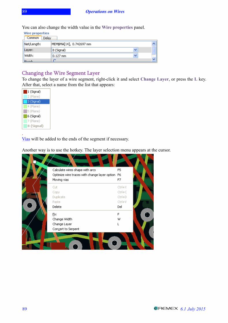
Changing the Wire Segment LayerTo change the layer of a wire segment, right-click it and select Change Layer, or press the L key.After that, select a name from the list that appears:
.Vias will be added to the ends of the segment if necessary.
Another way is to use the hotkey. The layer selection menu appears at the cursor.

90 Box selection
90 6.1 July 2015
Box selectionWhether an object (component, wire and so on) is affected by box selection depends on which waythe cursor is moving. If it is moving left to right (for example, from the lower left corner to the upperright), then only those objects become selected that are fully inside the selection box. If the cursor ismoving right to left (for example, from the lower right corner to the upper left), this selects all objectsthat are at least partially inside the box.
For details about other selection techniques, see Working with Components.
91 Working with Fixed Wires and Vias
91 6.1 July 2015
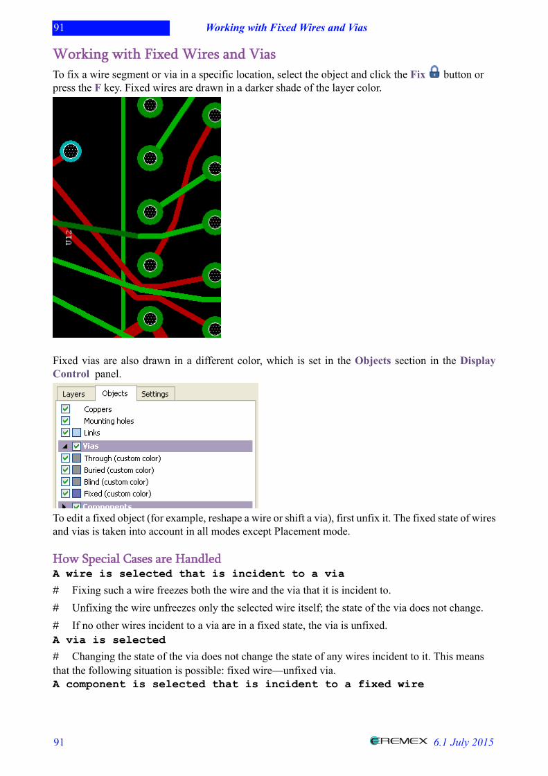
Working with Fixed Wires and ViasTo fix a wire segment or via in a specific location, select the object and click the Fix button orpress the F key. Fixed wires are drawn in a darker shade of the layer color.
Fixed vias are also drawn in a different color, which is set in the Objects section in the DisplayControl panel.
To edit a fixed object (for example, reshape a wire or shift a via), first unfix it. The fixed state of wiresand vias is taken into account in all modes except Placement mode.
How Special Cases are HandledA wire is selected that is incident to a via
# Fixing such a wire freezes both the wire and the via that it is incident to.# Unfixing the wire unfreezes only the selected wire itself; the state of the via does not change.# If no other wires incident to a via are in a fixed state, the via is unfixed.A via is selected
# Changing the state of the via does not change the state of any wires incident to it. This meansthat the following situation is possible: fixed wire—unfixed via.A component is selected that is incident to a fixed wire

92 Working with Fixed Wires and Vias
92 6.1 July 2015
# When such a component is moved, the shape of the fixed wire does not change. A flexiblelinking wire is created between the component and the original fixed wire.Moving components that are incident to fixed wires
# If there are fixed objects in the selection, the move operation is not available.# When you move a via or component that is incident to a fixed wire, an unfixed wire is createdbetween the object you are moving and the fixed wire.
93 Reassigning Functionally Equivalent Pads
93 6.1 July 2015
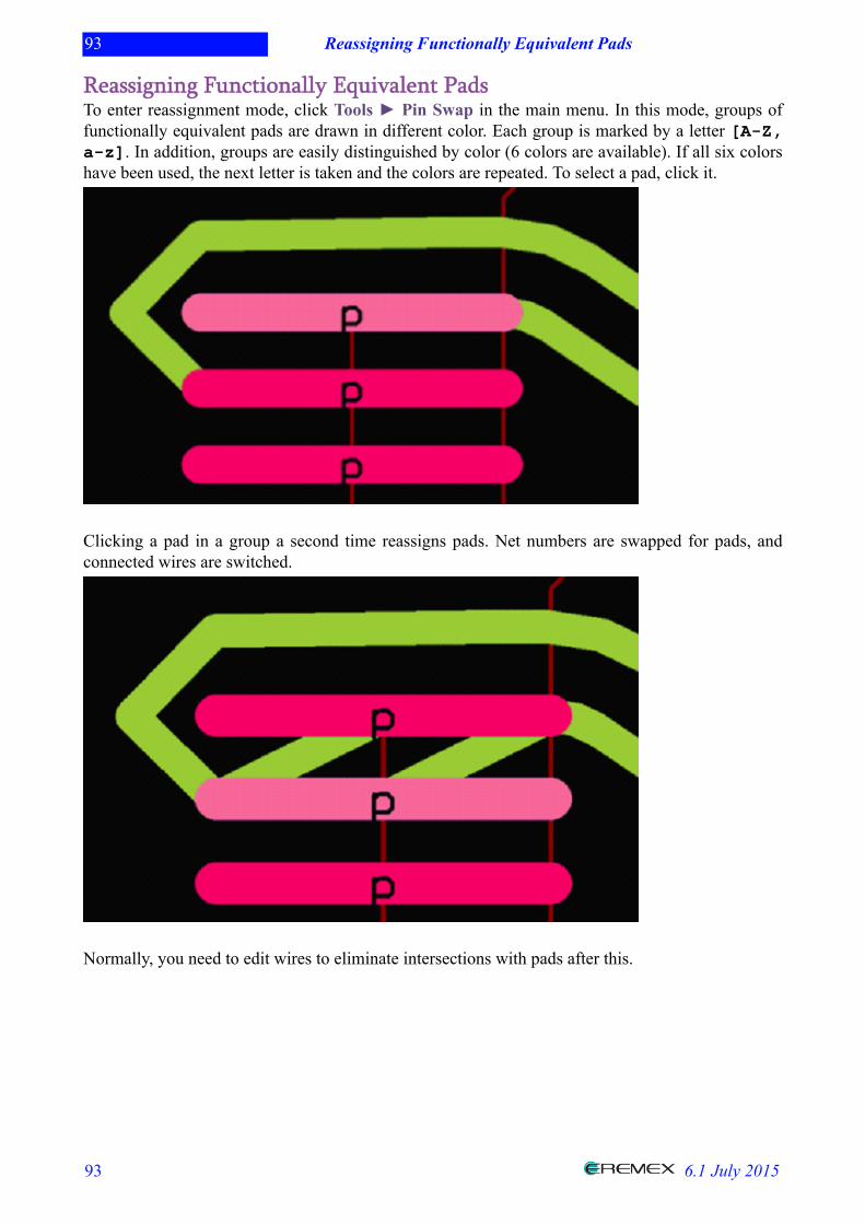
Reassigning Functionally Equivalent PadsTo enter reassignment mode, click Tools ► Pin Swap in the main menu. In this mode, groups offunctionally equivalent pads are drawn in different color. Each group is marked by a letter [A-Z,a-z]. In addition, groups are easily distinguished by color (6 colors are available). If all six colorshave been used, the next letter is taken and the colors are repeated. To select a pad, click it.
Clicking a pad in a group a second time reassigns pads. Net numbers are swapped for pads, andconnected wires are switched.
Normally, you need to edit wires to eliminate intersections with pads after this.
94 Reassigning Functionally Equivalent Pads
94 6.1 July 2015
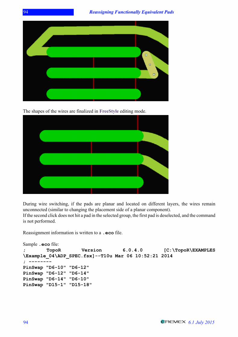
The shapes of the wires are finalized in FreeStyle editing mode.
During wire switching, if the pads are planar and located on different layers, the wires remainunconnected (similar to changing the placement side of a planar component).If the second click does not hit a pad in the selected group, the first pad is deselected, and the commandis not performed.
Reassignment information is written to a .eco file.
Sample .eco file:; TopoR Version 6.0.4.0 [C:\TopoR\EXAMPLES\Example_04\ADP_SPEC.fsx]--T10u Mar 06 10:52:21 2014; --------PinSwap "D6-10" "D6-12"PinSwap "D6-12" "D6-14"PinSwap "D6-14" "D6-10"PinSwap "D15-1" "D15-18"
95 Working with Text Labels
95 6.1 July 2015
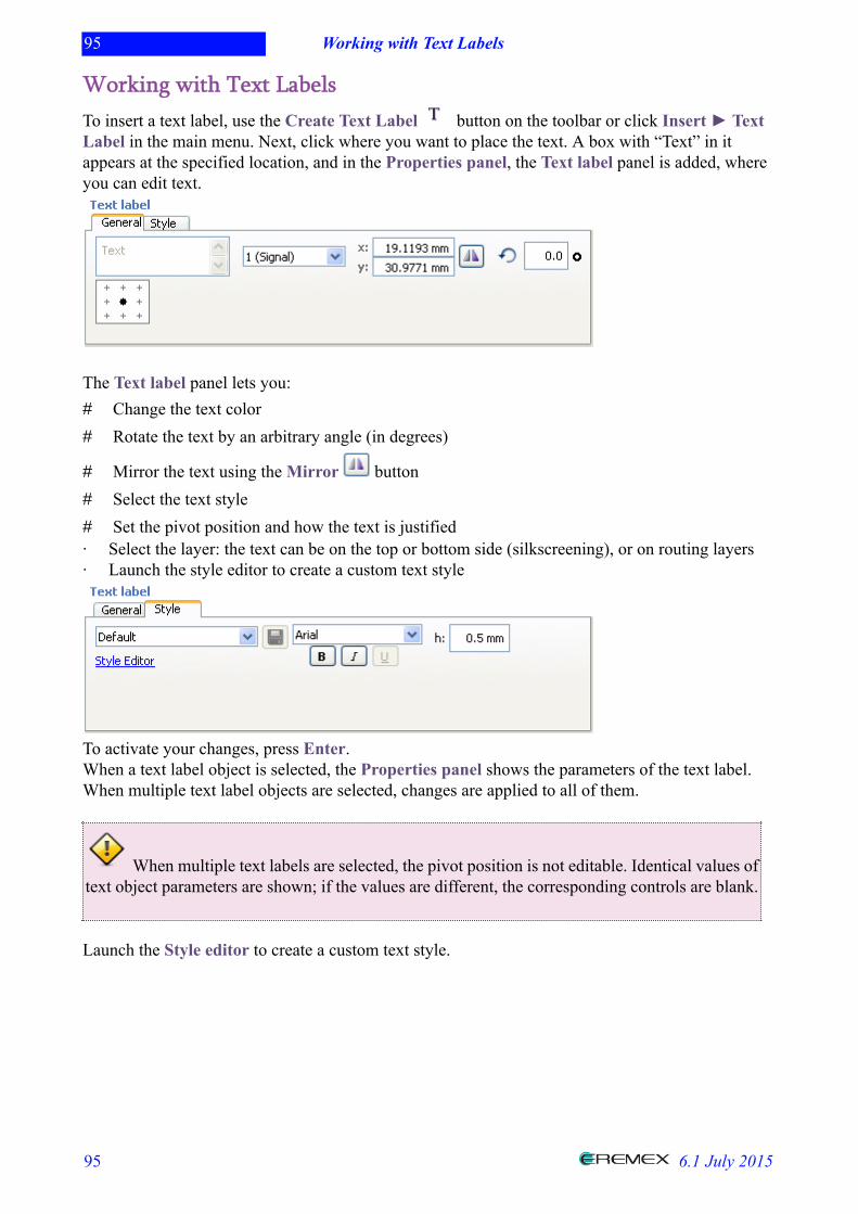
Working with Text LabelsTo insert a text label, use the Create Text Label button on the toolbar or click Insert ► TextLabel in the main menu. Next, click where you want to place the text. A box with “Text” in itappears at the specified location, and in the Properties panel, the Text label panel is added, whereyou can edit text.
The Text label panel lets you:# Change the text color# Rotate the text by an arbitrary angle (in degrees)
# Mirror the text using the Mirror button# Select the text style# Set the pivot position and how the text is justified· Select the layer: the text can be on the top or bottom side (silkscreening), or on routing layers· Launch the style editor to create a custom text style
To activate your changes, press Enter.When a text label object is selected, the Properties panel shows the parameters of the text label.When multiple text label objects are selected, changes are applied to all of them.
When multiple text labels are selected, the pivot position is not editable. Identical values oftext object parameters are shown; if the values are different, the corresponding controls are blank.
Launch the Style editor to create a custom text style.
96 Working with Text Labels
96 6.1 July 2015
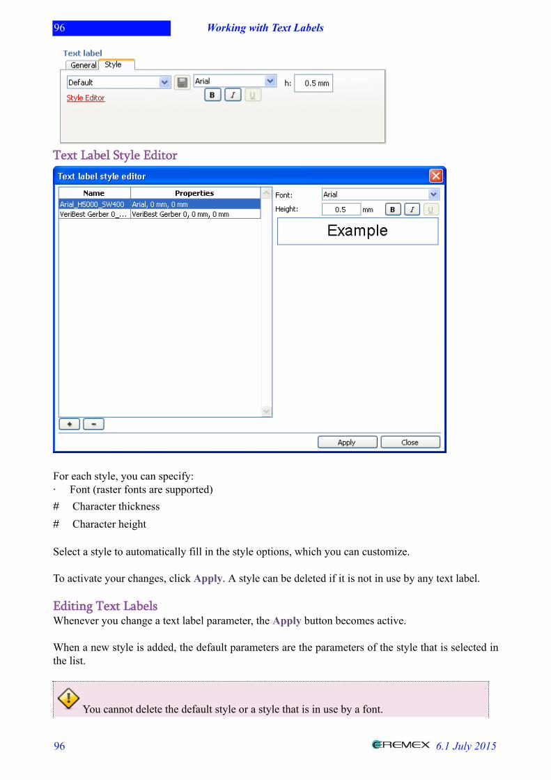
Text Label Style Editor
For each style, you can specify:· Font (raster fonts are supported)# Character thickness# Character height
Select a style to automatically fill in the style options, which you can customize.
To activate your changes, click Apply. A style can be deleted if it is not in use by any text label.
Editing Text LabelsWhenever you change a text label parameter, the Apply button becomes active.
When a new style is added, the default parameters are the parameters of the style that is selected inthe list.
You cannot delete the default style or a style that is in use by a font.
97 Working with Text Labels
97 6.1 July 2015
The default style is customizable. To select a font for any style, use the corresponding dialog box.
Fonts are not duplicated. The program uses the first font with the specified name that itcan find.
98 Creating PCB Outlines and Cutouts
98 6.1 July 2015
Creating PCB Outlines and CutoutsTo create the outline of the PCB, click the Create keepout button on the toolbar. This createsan outline with the currently selected shape. To change the shape, right-click the Create keepout
button and select the shape you need in the context menu.
After the primitive is drawn, set the line width on the General tab. You can adjust the outline shapein the PCB outline editor, on the Vertex tab, by editing vertex coordinates.
Cutouts are created likewise, but you need to set the Role to Board Cutout.
99 Creating Keepouts
99 6.1 July 2015
Creating KeepoutsTo create a keepout, click Insert ► Keepout in the main menu and select the primitive shape youwant from the drop-down menu.
After the keepout is drawn, configure its properties:
Next, set the keepout role: Routing Keepout or Placement Keepout.
For a placement keepout specify the restricted side (or sides):# Top# Bottom# Both
For a routing keepout specify what it affects:# Wires# Vias# Both wires and vias
After that, select one or more layers that the keepout applies to:
You can change shape of the keepout in the topology editor or in the keepout's Properties panel onthe Vertex tab by changing vertex coordinates.
100 Creating Keepouts
100 6.1 July 2015
101 Working with Copper Areas
101 6.1 July 2015
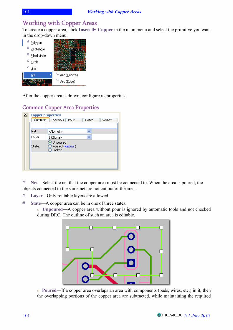
Working with Copper AreasTo create a copper area, click Insert ► Copper in the main menu and select the primitive you wantin the drop-down menu:
After the copper area is drawn, configure its properties.
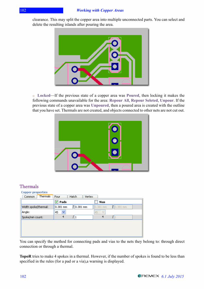
Common Copper Area Properties
# Net—Select the net that the copper area must be connected to. When the area is poured, theobjects connected to the same net are not cut out of the area.# Layer—Only routable layers are allowed.# State—A copper area can be in one of three states:
o Unpoured—A copper area without pour is ignored by automatic tools and not checkedduring DRC. The outline of such an area is editable.
o Poured—If a copper area overlaps an area with components (pads, wires, etc.) in it, thenthe overlapping portions of the copper area are subtracted, while maintaining the required
102 Working with Copper Areas
102 6.1 July 2015
clearance. This may split the copper area into multiple unconnected parts. You can select anddelete the resulting islands after pouring the area.
o Locked—If the previous state of a copper area was Poured, then locking it makes thefollowing commands unavailable for the area: Repour All, Repour Seleted, Unpour. If theprevious state of a copper area was Unpoured, then a poured area is created with the outlinethat you have set. Thermals are not created, and objects connected to other nets are not cut out.
Thermals
You can specify the method for connecting pads and vias to the nets they belong to: through directconnection or through a thermal.
TopoR tries to make 4 spokes in a thermal. However, if the number of spokes is found to be less thanspecified in the rules (for a pad or a via),a warning is displayed.
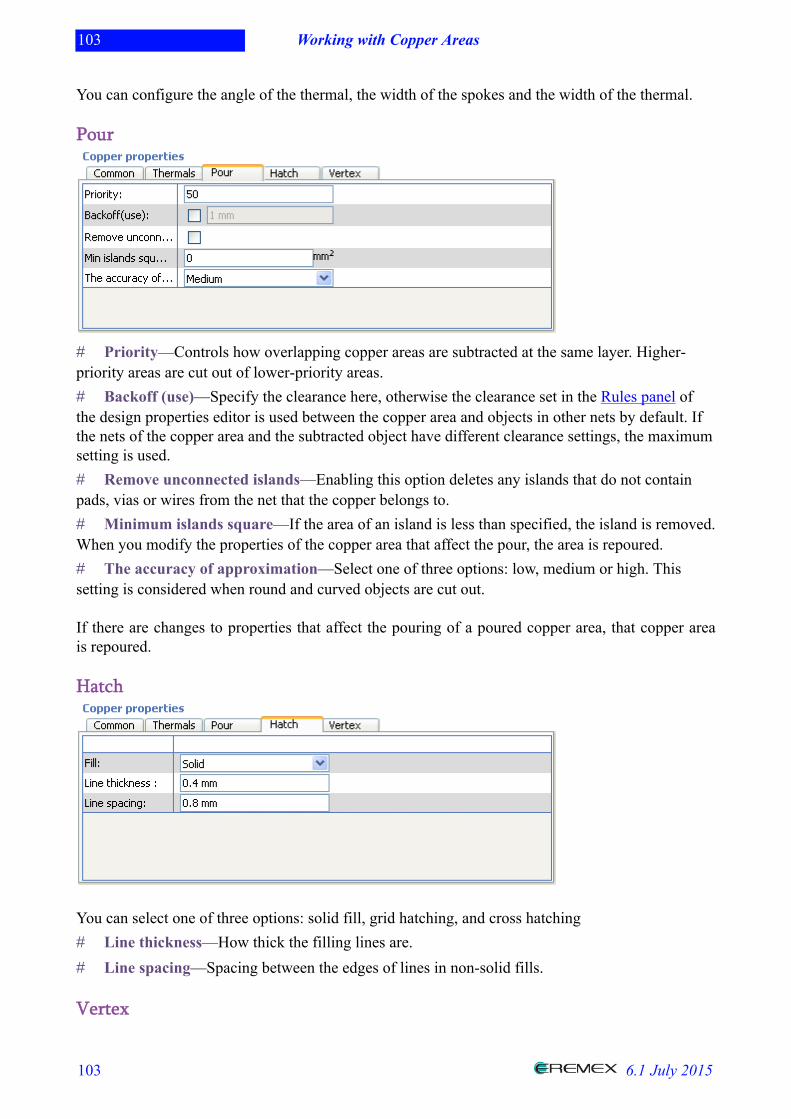
103 Working with Copper Areas
103 6.1 July 2015
You can configure the angle of the thermal, the width of the spokes and the width of the thermal.
Pour
# Priority—Controls how overlapping copper areas are subtracted at the same layer. Higher-priority areas are cut out of lower-priority areas.# Backoff (use)—Specify the clearance here, otherwise the clearance set in the Rules panel ofthe design properties editor is used between the copper area and objects in other nets by default. Ifthe nets of the copper area and the subtracted object have different clearance settings, the maximumsetting is used.# Remove unconnected islands—Enabling this option deletes any islands that do not containpads, vias or wires from the net that the copper belongs to.# Minimum islands square—If the area of an island is less than specified, the island is removed.When you modify the properties of the copper area that affect the pour, the area is repoured.# The accuracy of approximation—Select one of three options: low, medium or high. Thissetting is considered when round and curved objects are cut out.
If there are changes to properties that affect the pouring of a poured copper area, that copper areais repoured.
Hatch
You can select one of three options: solid fill, grid hatching, and cross hatching# Line thickness—How thick the filling lines are.# Line spacing—Spacing between the edges of lines in non-solid fills.
Vertex
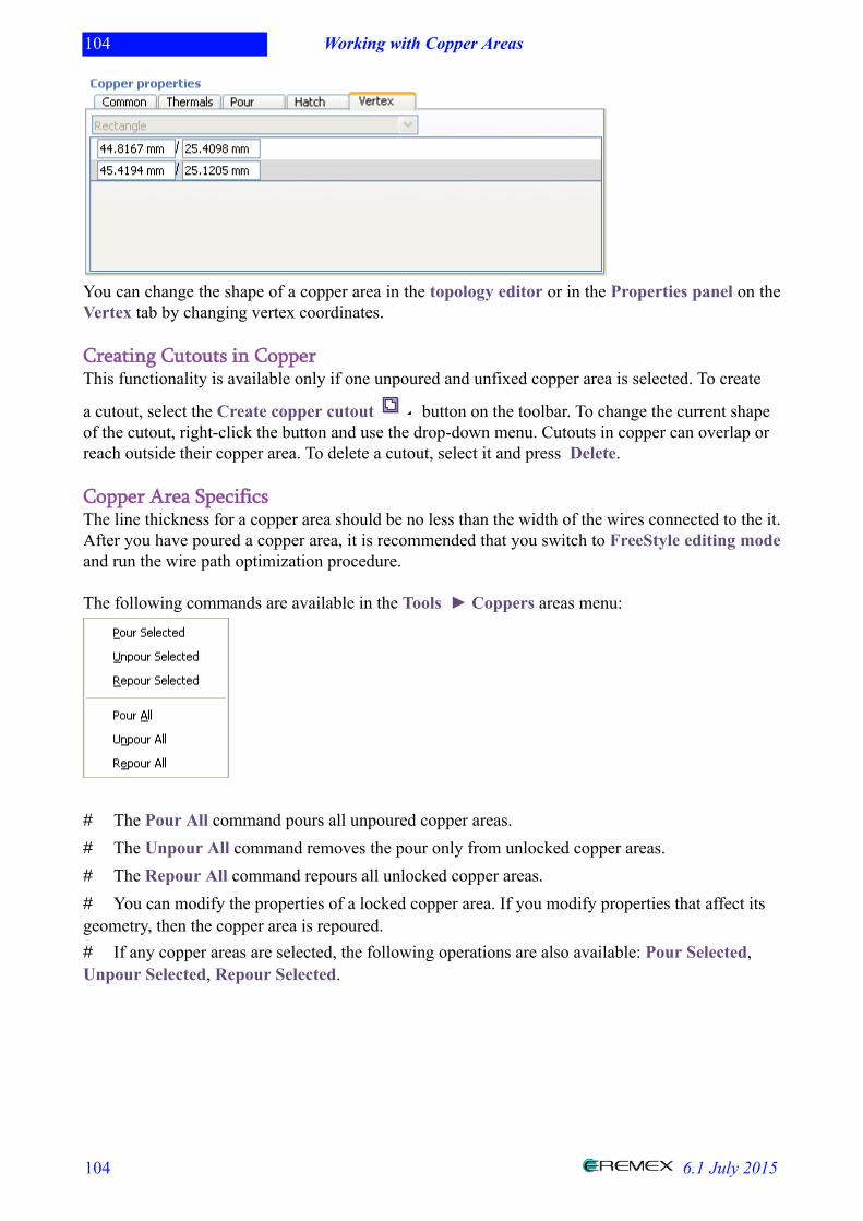
104 Working with Copper Areas
104 6.1 July 2015
You can change the shape of a copper area in the topology editor or in the Properties panel on theVertex tab by changing vertex coordinates.
Creating Cutouts in CopperThis functionality is available only if one unpoured and unfixed copper area is selected. To create
a cutout, select the Create copper cutout button on the toolbar. To change the current shapeof the cutout, right-click the button and use the drop-down menu. Cutouts in copper can overlap orreach outside their copper area. To delete a cutout, select it and press Delete.
Copper Area SpecificsThe line thickness for a copper area should be no less than the width of the wires connected to the it.After you have poured a copper area, it is recommended that you switch to FreeStyle editing modeand run the wire path optimization procedure.
The following commands are available in the Tools ► Coppers areas menu:
# The Pour All command pours all unpoured copper areas.# The Unpour All command removes the pour only from unlocked copper areas.# The Repour All command repours all unlocked copper areas.# You can modify the properties of a locked copper area. If you modify properties that affect itsgeometry, then the copper area is repoured.# If any copper areas are selected, the following operations are also available: Pour Selected,Unpour Selected, Repour Selected.
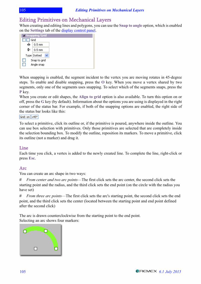
105 Editing Primitives on Mechanical Layers
105 6.1 July 2015
Editing Primitives on Mechanical LayersWhen creating and editing lines and polygons, you can use the Snap to angle option, which is enabledon the Settings tab of the display control panel.
When snapping is enabled, the segment incident to the vertex you are moving rotates in 45-degreesteps. To enable and disable snapping, press the O key. When you move a vertex shared by twosegments, only one of the segments uses snapping. To select which of the segments snaps, press theP key.When you create or edit shapes, the Align to grid option is also available. To turn this option on oroff, press the G key (by default). Information about the options you are using is displayed in the rightcorner of the status bar. For example, if both of the snapping options are enabled, the right side ofthe status bar looks like this:
To select a primitive, click its outline or, if the primitive is poured, anywhere inside the outline. Youcan use box selection with primitives. Only those primitives are selected that are completely insidethe selection bounding box. To modify the outline, reposition its markers. To move a primitive, clickits outline (not a marker) and drag it.
LineEach time you click, a vertex is added to the newly created line. To complete the line, right-click orpress Esc.
ArcYou can create an arc shape in two ways:# From center and two arc points—The first click sets the arc center, the second click sets thestarting point and the radius, and the third click sets the end point (on the circle with the radius youhave set)# From three arc points—The first click sets the arc's starting point, the second click sets the endpoint, and the third click sets the center (located between the starting point and end point definedafter the second click)
The arc is drawn counterclockwise from the starting point to the end point.Selecting an arc shows four markers:
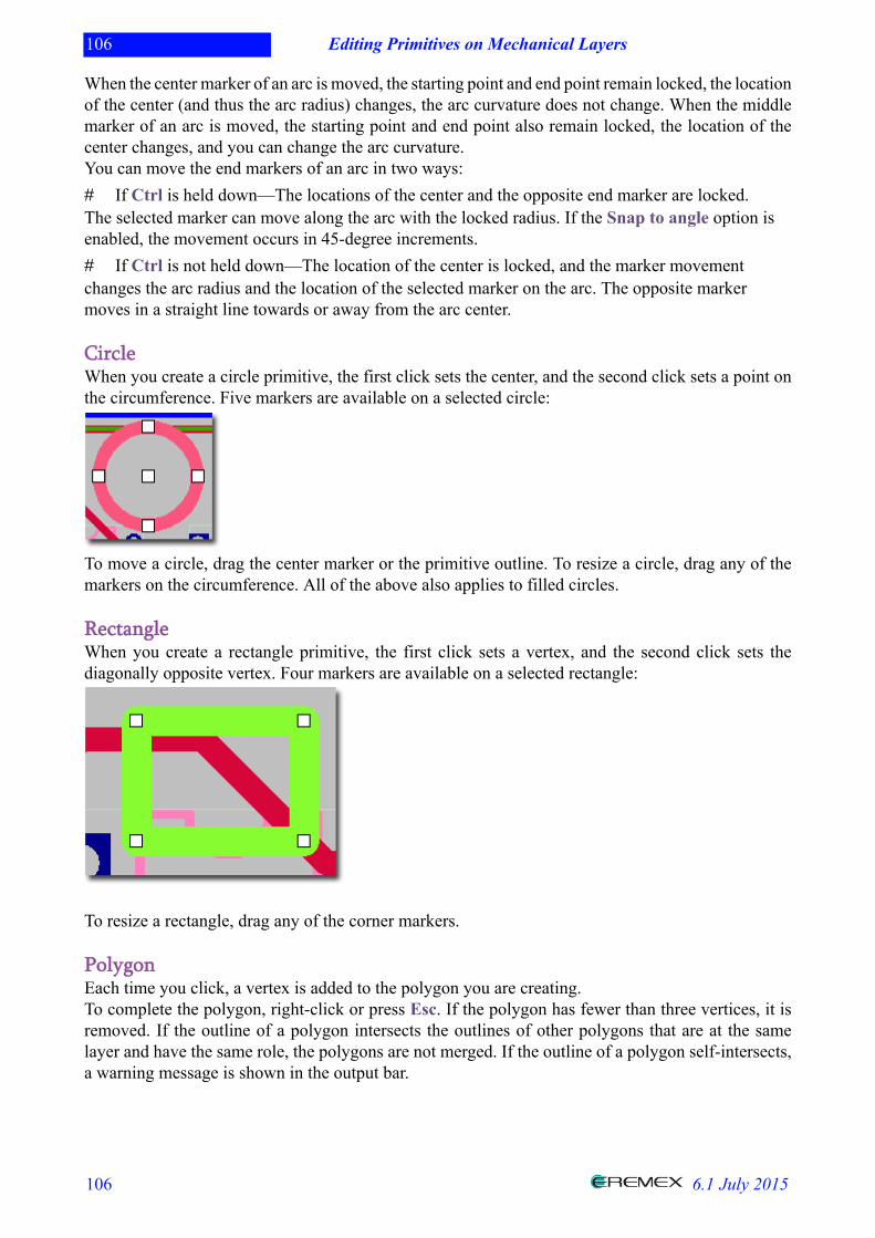
106 Editing Primitives on Mechanical Layers
106 6.1 July 2015
When the center marker of an arc is moved, the starting point and end point remain locked, the locationof the center (and thus the arc radius) changes, the arc curvature does not change. When the middlemarker of an arc is moved, the starting point and end point also remain locked, the location of thecenter changes, and you can change the arc curvature.You can move the end markers of an arc in two ways:# If Ctrl is held down—The locations of the center and the opposite end marker are locked.The selected marker can move along the arc with the locked radius. If the Snap to angle option isenabled, the movement occurs in 45-degree increments.# If Ctrl is not held down—The location of the center is locked, and the marker movementchanges the arc radius and the location of the selected marker on the arc. The opposite markermoves in a straight line towards or away from the arc center.
CircleWhen you create a circle primitive, the first click sets the center, and the second click sets a point onthe circumference. Five markers are available on a selected circle:
To move a circle, drag the center marker or the primitive outline. To resize a circle, drag any of themarkers on the circumference. All of the above also applies to filled circles.
RectangleWhen you create a rectangle primitive, the first click sets a vertex, and the second click sets thediagonally opposite vertex. Four markers are available on a selected rectangle:
To resize a rectangle, drag any of the corner markers.
PolygonEach time you click, a vertex is added to the polygon you are creating.To complete the polygon, right-click or press Esc. If the polygon has fewer than three vertices, it isremoved. If the outline of a polygon intersects the outlines of other polygons that are at the samelayer and have the same role, the polygons are not merged. If the outline of a polygon self-intersects,a warning message is shown in the output bar.
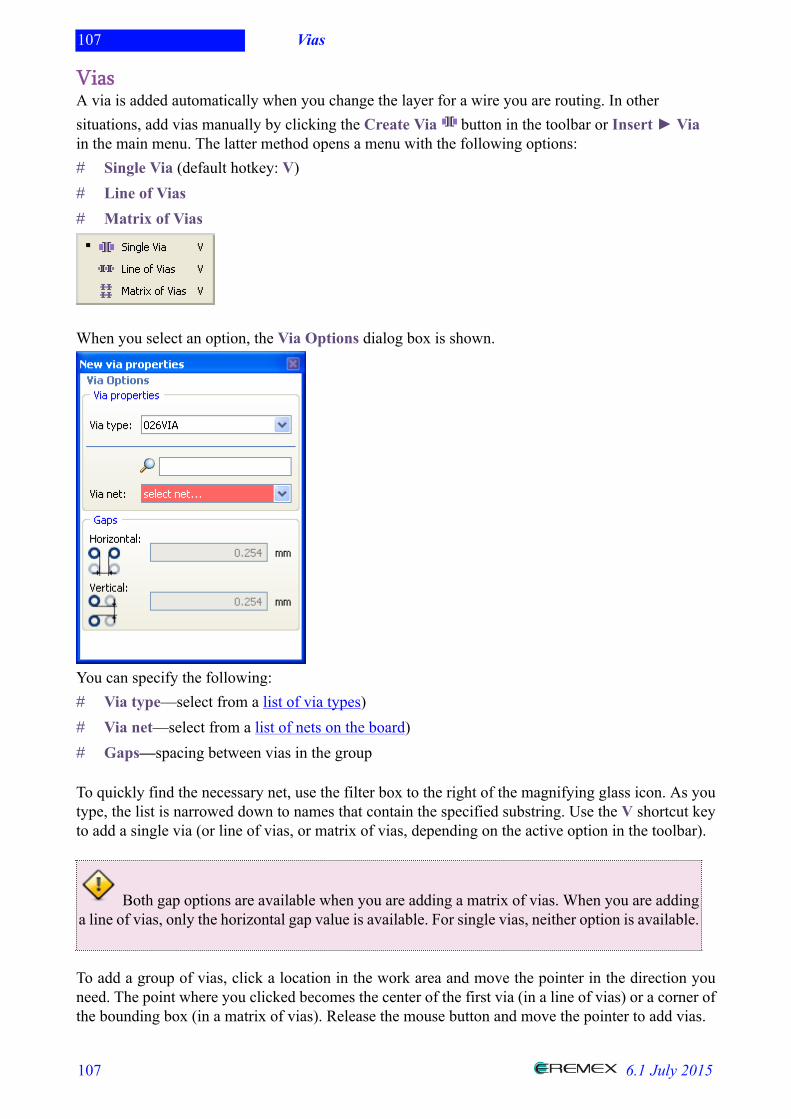
107 Vias
107 6.1 July 2015
ViasA via is added automatically when you change the layer for a wire you are routing. In othersituations, add vias manually by clicking the Create Via button in the toolbar or Insert ► Viain the main menu. The latter method opens a menu with the following options:# Single Via (default hotkey: V)# Line of Vias# Matrix of Vias
When you select an option, the Via Options dialog box is shown.
You can specify the following:# Via type—select from a list of via types)# Via net—select from a list of nets on the board)# Gaps—spacing between vias in the group
To quickly find the necessary net, use the filter box to the right of the magnifying glass icon. As youtype, the list is narrowed down to names that contain the specified substring. Use the V shortcut keyto add a single via (or line of vias, or matrix of vias, depending on the active option in the toolbar).
Both gap options are available when you are adding a matrix of vias. When you are addinga line of vias, only the horizontal gap value is available. For single vias, neither option is available.
To add a group of vias, click a location in the work area and move the pointer in the direction youneed. The point where you clicked becomes the center of the first via (in a line of vias) or a corner ofthe bounding box (in a matrix of vias). Release the mouse button and move the pointer to add vias.
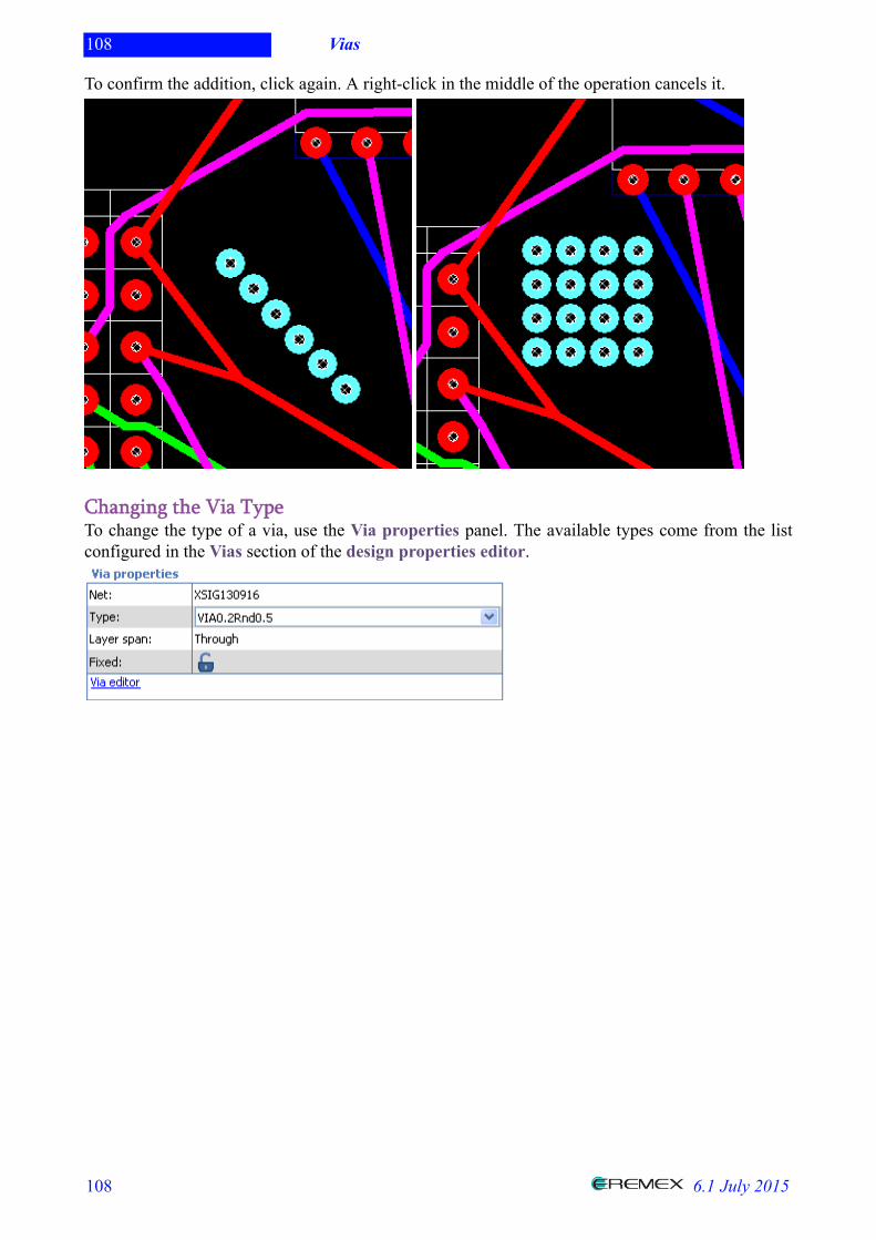
108 Vias
108 6.1 July 2015
To confirm the addition, click again. A right-click in the middle of the operation cancels it.
Changing the Via TypeTo change the type of a via, use the Via properties panel. The available types come from the listconfigured in the Vias section of the design properties editor.
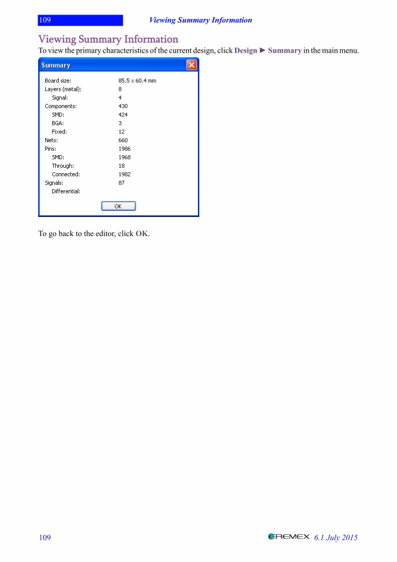
109 Viewing Summary Information
109 6.1 July 2015
Viewing Summary InformationTo view the primary characteristics of the current design, click Design ► Summary in the main menu.
To go back to the editor, click OK.
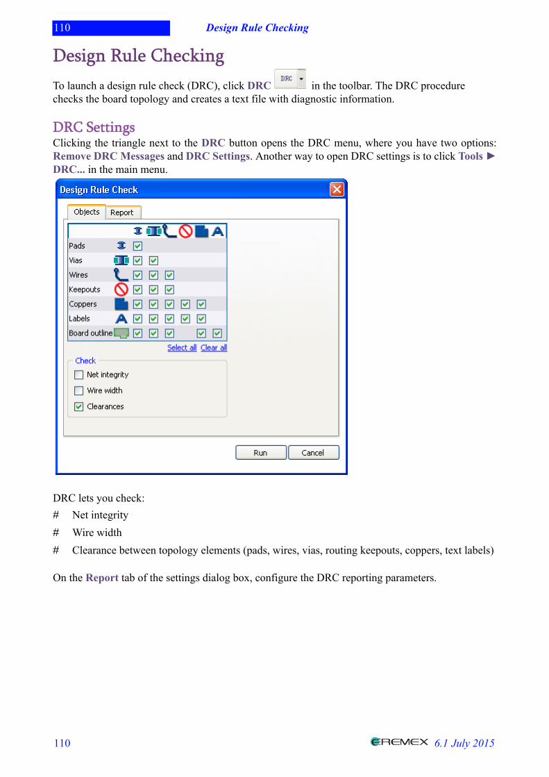
110 Design Rule Checking
110 6.1 July 2015
Design Rule CheckingTo launch a design rule check (DRC), click DRC in the toolbar. The DRC procedurechecks the board topology and creates a text file with diagnostic information. DRC SettingsClicking the triangle next to the DRC button opens the DRC menu, where you have two options:Remove DRC Messages and DRC Settings. Another way to open DRC settings is to click Tools ►DRC... in the main menu.
DRC lets you check:# Net integrity# Wire width# Clearance between topology elements (pads, wires, vias, routing keepouts, coppers, text labels)
On the Report tab of the settings dialog box, configure the DRC reporting parameters.
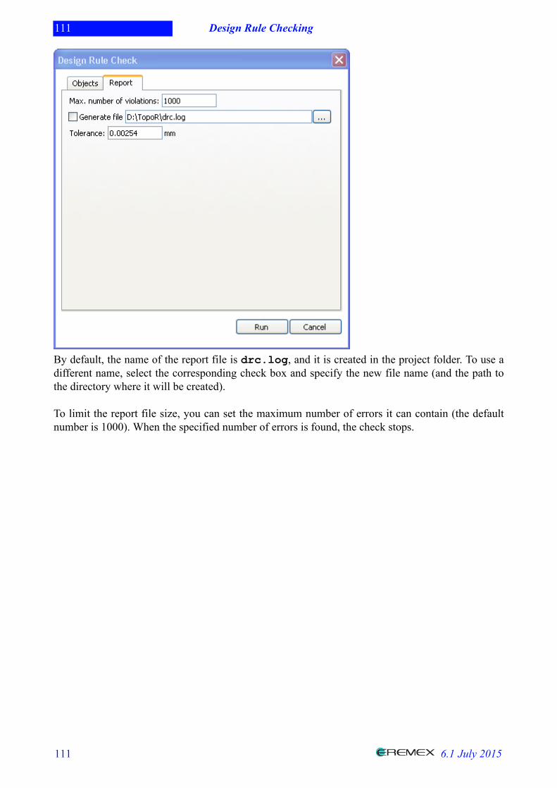
111 Design Rule Checking
111 6.1 July 2015
By default, the name of the report file is drc.log, and it is created in the project folder. To use adifferent name, select the corresponding check box and specify the new file name (and the path tothe directory where it will be created).
To limit the report file size, you can set the maximum number of errors it can contain (the defaultnumber is 1000). When the specified number of errors is found, the check stops.

112 Writing Results
112 6.1 July 2015
Writing ResultsThe final step in working on a project in TopoR is to write output files.
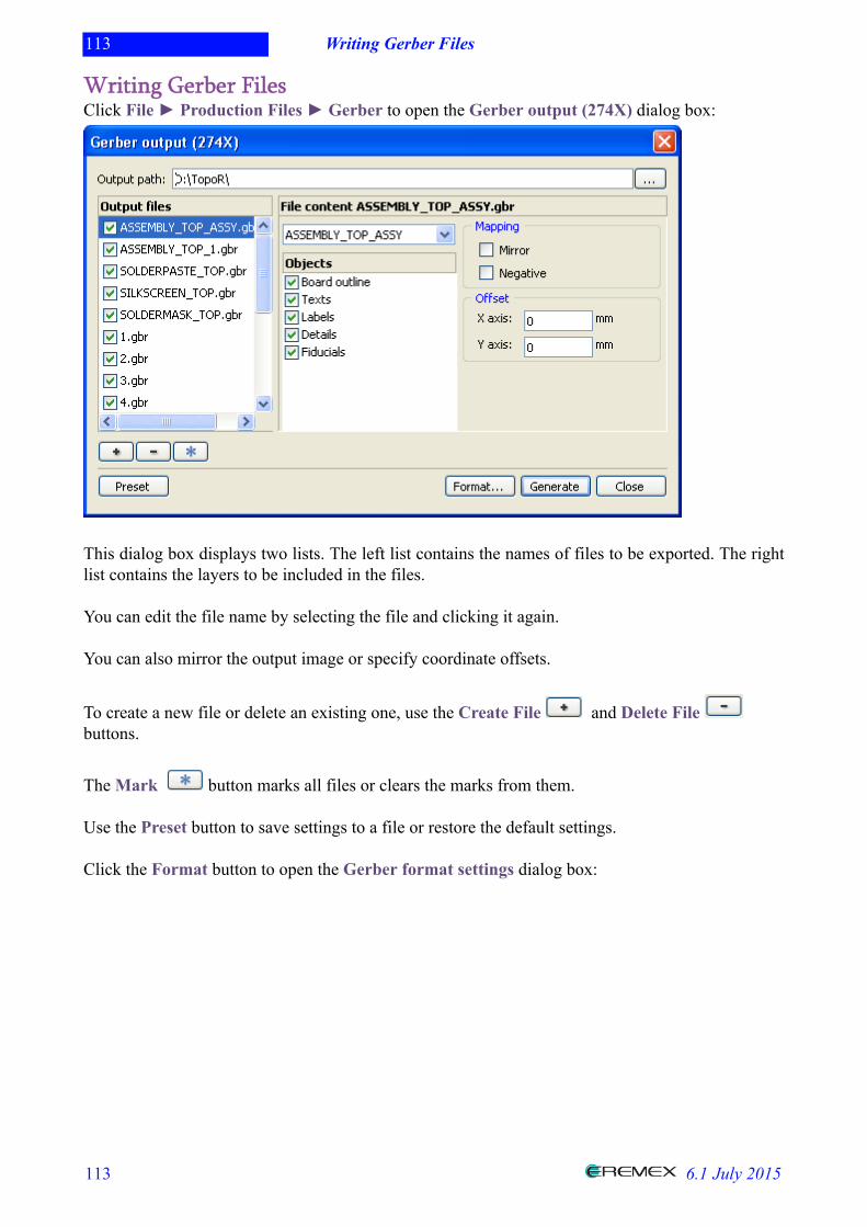
113 Writing Gerber Files
113 6.1 July 2015
Writing Gerber FilesClick File ► Production Files ► Gerber to open the Gerber output (274X) dialog box:
This dialog box displays two lists. The left list contains the names of files to be exported. The rightlist contains the layers to be included in the files.
You can edit the file name by selecting the file and clicking it again.
You can also mirror the output image or specify coordinate offsets.
To create a new file or delete an existing one, use the Create File and Delete File buttons.
The Mark button marks all files or clears the marks from them.
Use the Preset button to save settings to a file or restore the default settings.
Click the Format button to open the Gerber format settings dialog box:
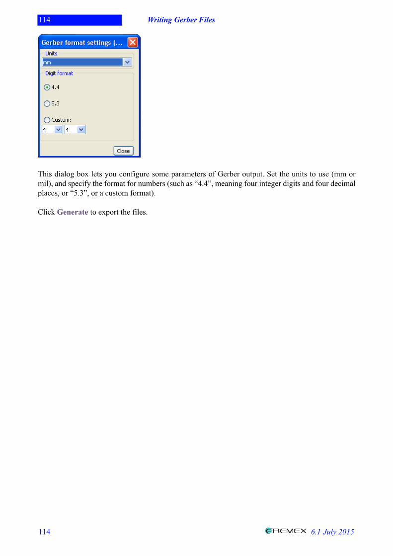
114 Writing Gerber Files
114 6.1 July 2015
This dialog box lets you configure some parameters of Gerber output. Set the units to use (mm ormil), and specify the format for numbers (such as “4.4”, meaning four integer digits and four decimalplaces, or “5.3”, or a custom format).
Click Generate to export the files.
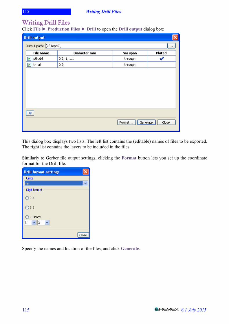
115 Writing Drill Files
115 6.1 July 2015
Writing Drill FilesClick File ► Production Files ► Drill to open the Drill output dialog box:
This dialog box displays two lists. The left list contains the (editable) names of files to be exported.The right list contains the layers to be included in the files.
Similarly to Gerber file output settings, clicking the Format button lets you set up the coordinateformat for the Drill file.
Specify the names and location of the files, and click Generate.
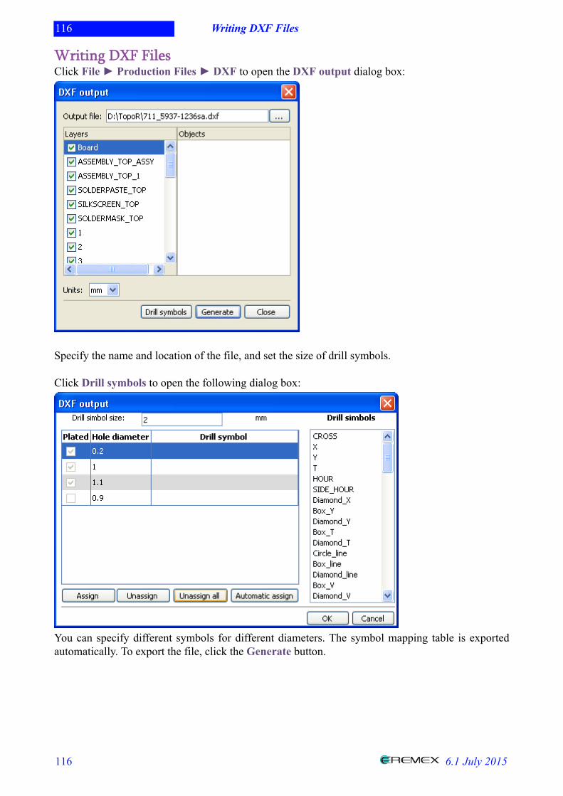
116 Writing DXF Files
116 6.1 July 2015
Writing DXF FilesClick File ► Production Files ► DXF to open the DXF output dialog box:
Specify the name and location of the file, and set the size of drill symbols.
Click Drill symbols to open the following dialog box:
You can specify different symbols for different diameters. The symbol mapping table is exportedautomatically. To export the file, click the Generate button.
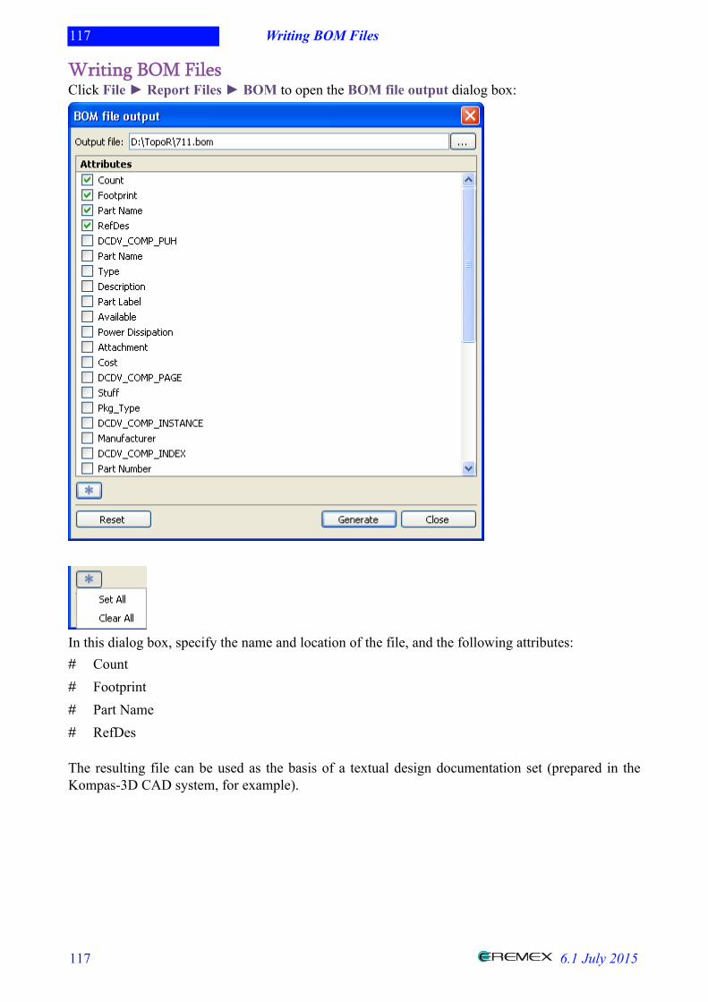
117 Writing BOM Files
117 6.1 July 2015
Writing BOM FilesClick File ► Report Files ► BOM to open the BOM file output dialog box:
In this dialog box, specify the name and location of the file, and the following attributes:# Count# Footprint# Part Name# RefDes
The resulting file can be used as the basis of a textual design documentation set (prepared in theKompas-3D CAD system, for example).
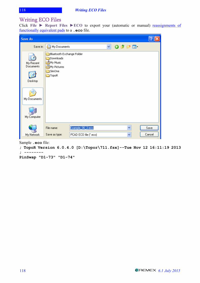
118 Writing ECO Files
118 6.1 July 2015
Writing ECO FilesClick File ► Report Files ►ECO to export your (automatic or manual) reassignments offunctionally equivalent pads to a .eco file.
Sample .eco file:; TopoR Version 6.0.4.0 [D:\Topor\711.fsx]--Tue Nov 12 16:11:19 2013; --------PinSwap "D1-73" "D1-74"
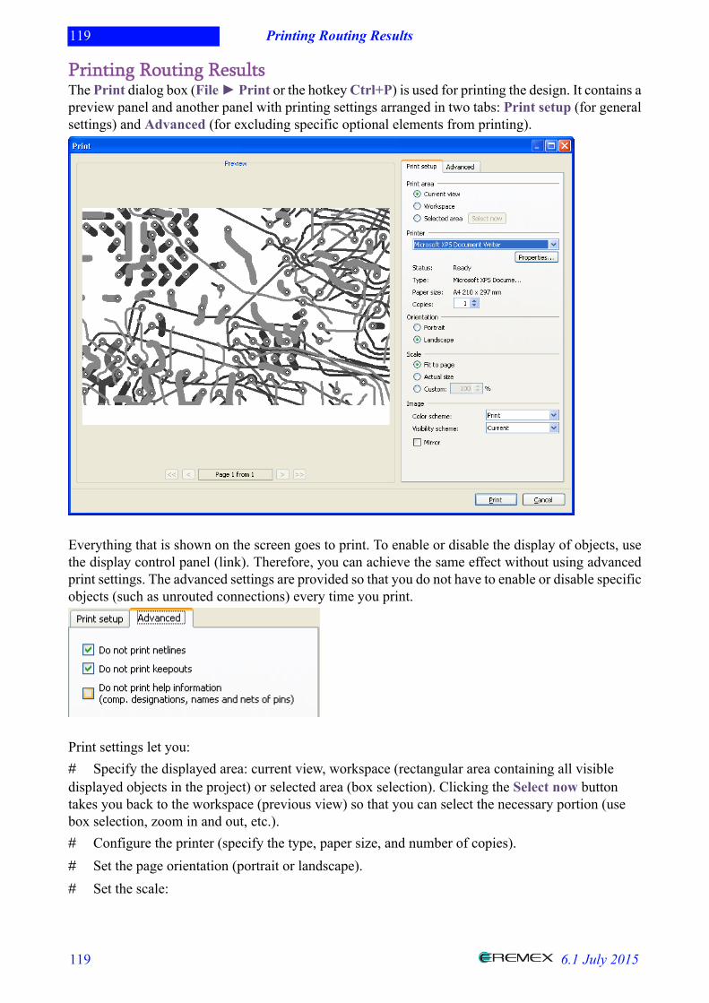
119 Printing Routing Results
119 6.1 July 2015
Printing Routing ResultsThe Print dialog box (File ► Print or the hotkey Ctrl+P) is used for printing the design. It contains apreview panel and another panel with printing settings arranged in two tabs: Print setup (for generalsettings) and Advanced (for excluding specific optional elements from printing).
Everything that is shown on the screen goes to print. To enable or disable the display of objects, usethe display control panel (link). Therefore, you can achieve the same effect without using advancedprint settings. The advanced settings are provided so that you do not have to enable or disable specificobjects (such as unrouted connections) every time you print.
Print settings let you:# Specify the displayed area: current view, workspace (rectangular area containing all visibledisplayed objects in the project) or selected area (box selection). Clicking the Select now buttontakes you back to the workspace (previous view) so that you can select the necessary portion (usebox selection, zoom in and out, etc.).# Configure the printer (specify the type, paper size, and number of copies).# Set the page orientation (portrait or landscape).# Set the scale:
120 Printing Routing Results
120 6.1 July 2015
• Fit the image to the page (enlarge or shrink it to match the paper size)• Actual size (a scale of 1:1)• Custom (a user-defined percentage; if the image does not fit in the page, it is printed over
multiple pages)
# Specify the image properties:
• The color scheme (print or grayscale)• The display scheme• Whether to mirror the image.
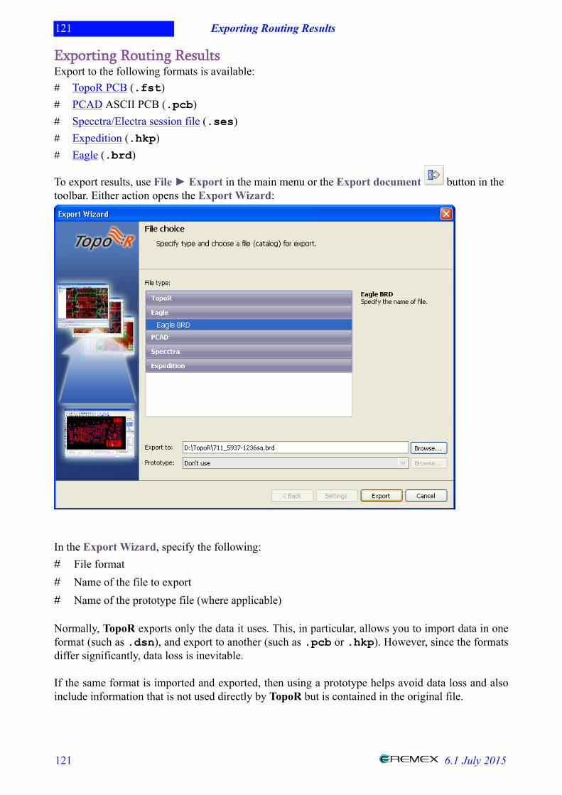
121 Exporting Routing Results
121 6.1 July 2015
Exporting Routing ResultsExport to the following formats is available:# TopoR PCB (.fst)# PCAD ASCII PCB (.pcb)# Specctra/Electra session file (.ses)# Expedition (.hkp)# Eagle (.brd)
To export results, use File ► Export in the main menu or the Export document button in thetoolbar. Either action opens the Export Wizard:
In the Export Wizard, specify the following:# File format# Name of the file to export# Name of the prototype file (where applicable)
Normally, TopoR exports only the data it uses. This, in particular, allows you to import data in oneformat (such as .dsn), and export to another (such as .pcb or .hkp). However, since the formatsdiffer significantly, data loss is inevitable.
If the same format is imported and exported, then using a prototype helps avoid data loss and alsoinclude information that is not used directly by TopoR but is contained in the original file.
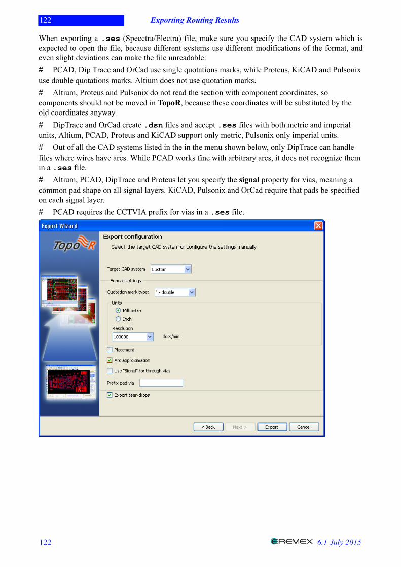
122 Exporting Routing Results
122 6.1 July 2015
When exporting a .ses (Specctra/Electra) file, make sure you specify the CAD system which isexpected to open the file, because different systems use different modifications of the format, andeven slight deviations can make the file unreadable:# PCAD, Dip Trace and OrCad use single quotations marks, while Proteus, KiCAD and Pulsonixuse double quotations marks. Altium does not use quotation marks.# Altium, Proteus and Pulsonix do not read the section with component coordinates, socomponents should not be moved in TopoR, because these coordinates will be substituted by theold coordinates anyway.# DipTrace and OrCad create .dsn files and accept .ses files with both metric and imperialunits, Altium, PCAD, Proteus and KiCAD support only metric, Pulsonix only imperial units.# Out of all the CAD systems listed in the in the menu shown below, only DipTrace can handlefiles where wires have arcs. While PCAD works fine with arbitrary arcs, it does not recognize themin a .ses file.# Altium, PCAD, DipTrace and Proteus let you specify the signal property for vias, meaning acommon pad shape on all signal layers. KiCAD, Pulsonix and OrCad require that pads be specifiedon each signal layer.# PCAD requires the CCTVIA prefix for vias in a .ses file.
123 C. Advanced Features
123 6.1 July 2015
C. Advanced FeaturesThis section is for experienced users of the software. Read on for information about TopoRfunctionality that is not covered in part B of this manual.

124 Designing High-Speed Appliances
124 6.1 July 2015
Designing High-Speed AppliancesThis section describes working with the signal object type. This object type has been introduced torepresent transfer lines for electric signals, and, compared to earlier TopoR versions, it provides moreaccurate baseline data for delay synchronization in transfer lines.
Each signal has one source and one receiver. Multiple signals can share a source. However, signalscannot share a receiver.
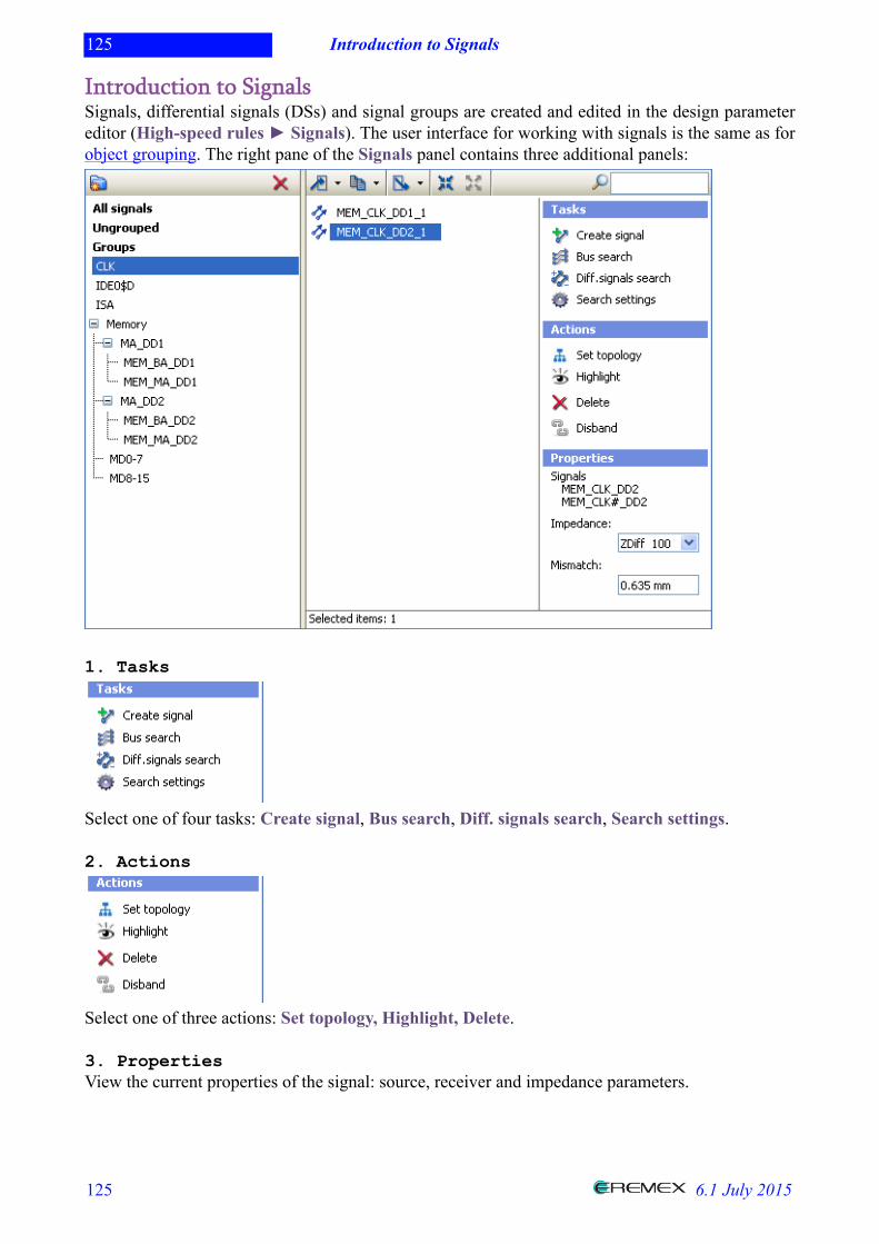
125 Introduction to Signals
125 6.1 July 2015
Introduction to SignalsSignals, differential signals (DSs) and signal groups are created and edited in the design parametereditor (High-speed rules ► Signals). The user interface for working with signals is the same as forobject grouping. The right pane of the Signals panel contains three additional panels:
1. Tasks
Select one of four tasks: Create signal, Bus search, Diff. signals search, Search settings.
2. Actions
Select one of three actions: Set topology, Highlight, Delete.
3. PropertiesView the current properties of the signal: source, receiver and impedance parameters.

126 Introduction to Signals
126 6.1 July 2015
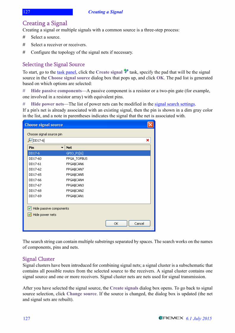
127 Creating a Signal
127 6.1 July 2015
Creating a SignalCreating a signal or multiple signals with a common source is a three-step process:# Select a source.# Select a receiver or receivers.# Configure the topology of the signal nets if necessary.
Selecting the Signal SourceTo start, go to the task panel, click the Create signal task, specify the pad that will be the signalsource in the Choose signal source dialog box that pops up, and click OK. The pad list is generatedbased on which options are selected:# Hide passive components—A passive component is a resistor or a two-pin gate (for example,one involved in a resistor array) with equivalent pins.# Hide power nets—The list of power nets can be modified in the signal search settings.If a pin's net is already associated with an existing signal, then the pin is shown in a dim gray colorin the list, and a note in parentheses indicates the signal that the net is associated with.
The search string can contain multiple substrings separated by spaces. The search works on the namesof components, pins and nets.
Signal ClusterSignal clusters have been introduced for combining signal nets; a signal cluster is a subschematic thatcontains all possible routes from the selected source to the receivers. A signal cluster contains onesignal source and one or more receivers. Signal cluster nets are nets used for signal transmission.
After you have selected the signal source, the Create signals dialog box opens. To go back to signalsource selection, click Change source. If the source is changed, the dialog box is updated (the netand signal sets are rebuilt).
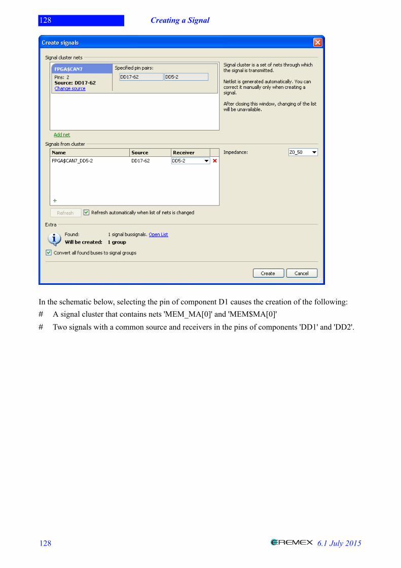
128 Creating a Signal
128 6.1 July 2015
In the schematic below, selecting the pin of component D1 causes the creation of the following:# A signal cluster that contains nets 'MEM_MA[0]' and 'MEM$MA[0]'# Two signals with a common source and receivers in the pins of components 'DD1' and 'DD2'.
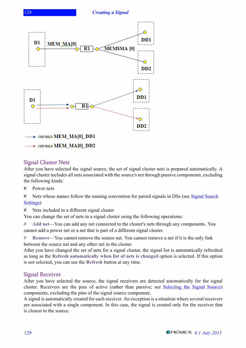
129 Creating a Signal
129 6.1 July 2015
Signal Cluster NetsAfter you have selected the signal source, the set of signal cluster nets is prepared automatically. Asignal cluster includes all nets associated with the source's net through passive components, excludingthe following kinds:# Power nets# Nets whose names follow the naming convention for paired signals in DSs (see Signal SearchSettings)# Nets included in a different signal clusterYou can change the set of nets in a signal cluster using the following operations:# Add net—You can add any net connected to the cluster's nets through any components. Youcannot add a power net or a net that is part of a different signal cluster.# Remove—You cannot remove the source net. You cannot remove a net if it is the only linkbetween the source net and any other net in the cluster.After you have changed the set of nets for a signal cluster, the signal list is automatically refreshedas long as the Refresh automatically when list of nets is changed option is selected. If this optionis not selected, you can use the Refresh button at any time.
Signal ReceiverAfter you have selected the source, the signal receivers are detected automatically for the signalcluster. Receivers are the pins of active (rather than passive; see Selecting the Signal Source)components, excluding the pins of the signal source component.A signal is automatically created for each receiver. An exception is a situation where several receiversare associated with a single component. In this case, the signal is created only for the receiver thatis closest to the source.
130 Creating a Signal
130 6.1 July 2015
The set of signals can be changed manually. Use the Add Signal button to add a signal to thesignal cluster. To remove a signal, use the button that is located in that signal's table row. Foreach signal, you can change the receiver pin to any pin in the signal cluster, including pins that arenot used by any signals.
If all pins have been turned into receivers, the button is not available.
To rename a signal, you can use the Create signals dialog box or the Signals panel. Duplicate namesfor signals (both regular and differential) are disallowed.
Setting the Net TopologyIf a signal cluster net has more than two pins, you can create pin pairs for it. For that, click the Addbutton and select the two pins that you want to connect. To add more pin pairs, use the button.
If the pin pairs you have configured form a contour, the following message is shown on the right:Contour is detected in net 'net_name', change pin pairs specificationPin pairs are configured automatically if the Create pin pairs automatically option is selected in theSignal search settings. Automatic pin pairs connect the signal source to every receiver.
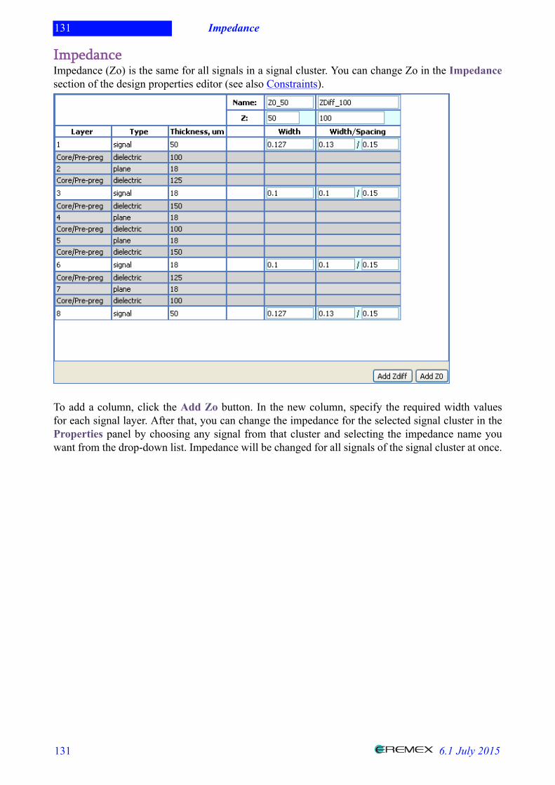
131 Impedance
131 6.1 July 2015
ImpedanceImpedance (Zo) is the same for all signals in a signal cluster. You can change Zo in the Impedancesection of the design properties editor (see also Constraints).
To add a column, click the Add Zo button. In the new column, specify the required width valuesfor each signal layer. After that, you can change the impedance for the selected signal cluster in theProperties panel by choosing any signal from that cluster and selecting the impedance name youwant from the drop-down list. Impedance will be changed for all signals of the signal cluster at once.
132 Using Signals
132 6.1 July 2015
Using SignalsThe primary use of signals is for signal delay synchronization rules. Signals can also be controlledby rules for inter-wire clearance and rules for assignment of via types inter-wire clearance rules andrules for via type assignment.
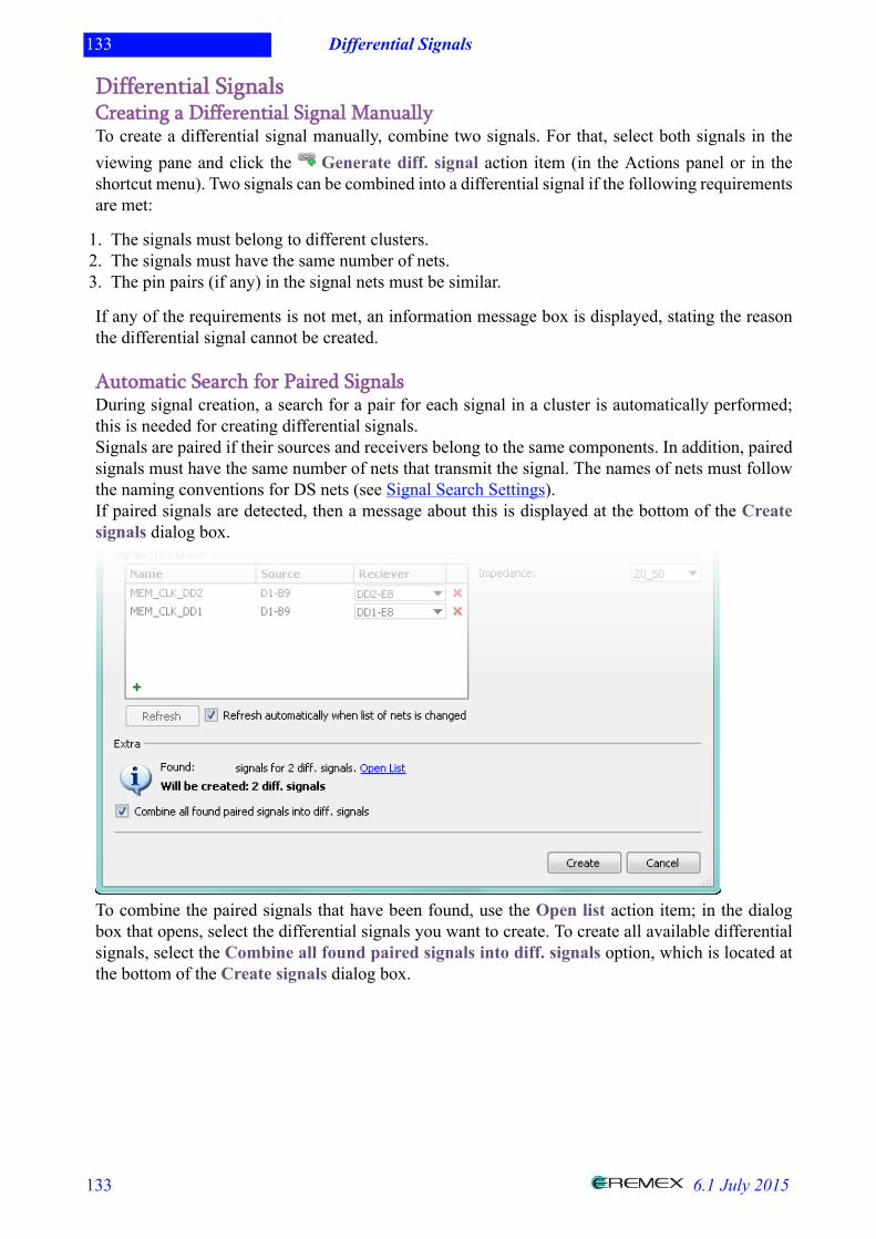
133 Differential Signals
133 6.1 July 2015
Differential SignalsCreating a Differential Signal ManuallyTo create a differential signal manually, combine two signals. For that, select both signals in theviewing pane and click the Generate diff. signal action item (in the Actions panel or in theshortcut menu). Two signals can be combined into a differential signal if the following requirementsare met:
1. The signals must belong to different clusters.2. The signals must have the same number of nets.3. The pin pairs (if any) in the signal nets must be similar.
If any of the requirements is not met, an information message box is displayed, stating the reasonthe differential signal cannot be created.
Automatic Search for Paired SignalsDuring signal creation, a search for a pair for each signal in a cluster is automatically performed;this is needed for creating differential signals.Signals are paired if their sources and receivers belong to the same components. In addition, pairedsignals must have the same number of nets that transmit the signal. The names of nets must followthe naming conventions for DS nets (see Signal Search Settings).If paired signals are detected, then a message about this is displayed at the bottom of the Createsignals dialog box.
To combine the paired signals that have been found, use the Open list action item; in the dialogbox that opens, select the differential signals you want to create. To create all available differentialsignals, select the Combine all found paired signals into diff. signals option, which is located atthe bottom of the Create signals dialog box.
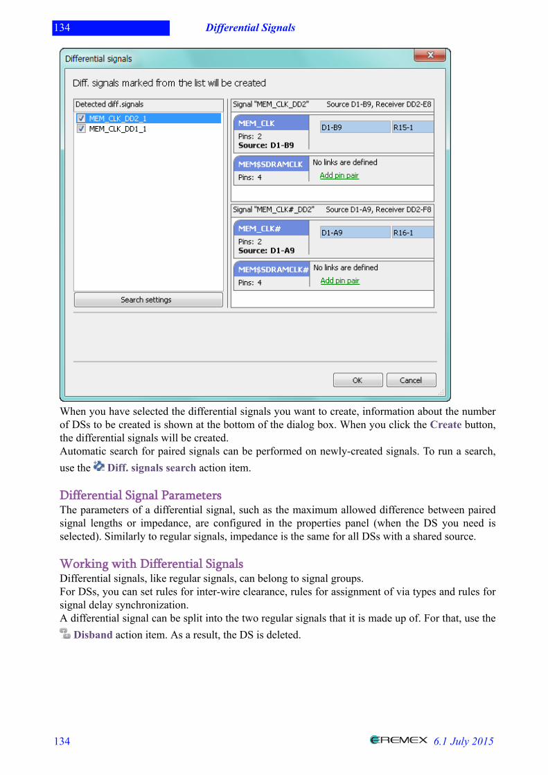
134 Differential Signals
134 6.1 July 2015
When you have selected the differential signals you want to create, information about the numberof DSs to be created is shown at the bottom of the dialog box. When you click the Create button,the differential signals will be created.Automatic search for paired signals can be performed on newly-created signals. To run a search,use the Diff. signals search action item.
Differential Signal ParametersThe parameters of a differential signal, such as the maximum allowed difference between pairedsignal lengths or impedance, are configured in the properties panel (when the DS you need isselected). Similarly to regular signals, impedance is the same for all DSs with a shared source.
Working with Differential SignalsDifferential signals, like regular signals, can belong to signal groups.For DSs, you can set rules for inter-wire clearance, rules for assignment of via types and rules forsignal delay synchronization.A differential signal can be split into the two regular signals that it is made up of. For that, use the
Disband action item. As a result, the DS is deleted.

135 Automatic Search for Signal Buses
135 6.1 July 2015
Automatic Search for Signal BusesWhen signals are created, searches for the signal bus are performed for each signal in the cluster. Bussignals are signals whose sources and receivers belong to the same components. The names of signalsources can differ in the index they use. An index is an arbitrary chain of digits, sometimes enclosedin parentheses or square brackets.
If signal buses are detected, a message about this is shown at the bottom of the Create signals dialogbox.
To create signal groups out of the signals in the buses that have been found, use the Open list actionitem. In the dialog box that pops up, select all buses that you want to convert to groups. To create allavailable signal groups, select the Convert all found buses to signal groups option at the bottomof the Create signals dialog box. When you have selected the signal groups to create, the resulting number of groups is shown at thebottom of the Create signals dialog box. To proceed, click the Create button.
Automatic search for signal buses can also be performed on existing signals. To run a search, usethe Bus search task in the signal panel action pane.
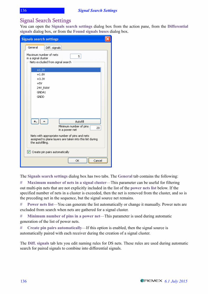
136 Signal Search Settings
136 6.1 July 2015
Signal Search SettingsYou can open the Signals search settings dialog box from the action pane, from the Differentialsignals dialog box, or from the Found signals buses dialog box.
The Signals search settings dialog box has two tabs. The General tab contains the following:# Maximum number of nets in a signal cluster—This parameter can be useful for filteringout multi-pin nets that are not explicitly included in the list of the power nets list below. If thespecified number of nets in a cluster is exceeded, then the net is removed from the cluster, and so isthe preceding net in the sequence, but the signal source net remains.# Power nets list—You can generate the list automatically or change it manually. Power nets areexcluded from search when nets are gathered for a signal cluster.# Minimum number of pins in a power net—This parameter is used during automaticgeneration of the list of power nets.# Create pin pairs automatically—If this option is enabled, then the signal source isautomatically paired with each receiver during the creation of a signal cluster.
The Diff. signals tab lets you edit naming rules for DS nets. These rules are used during automaticsearch for paired signals to combine into differential signals.
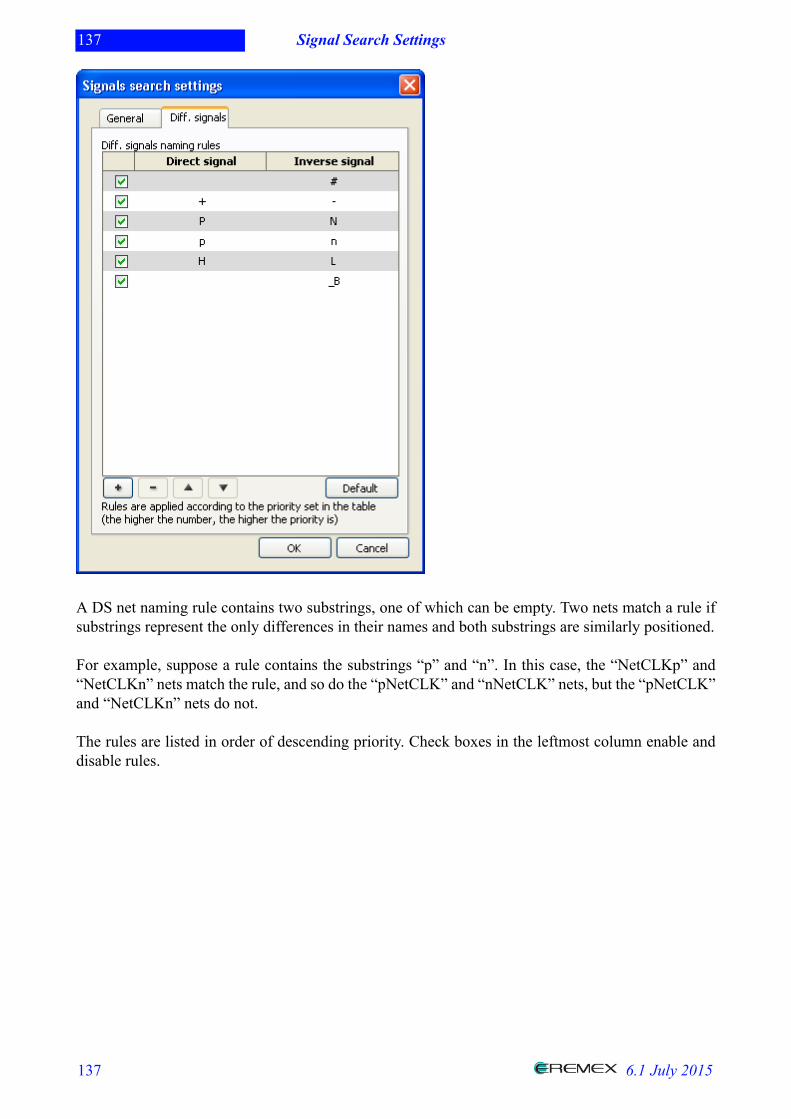
137 Signal Search Settings
137 6.1 July 2015
A DS net naming rule contains two substrings, one of which can be empty. Two nets match a rule ifsubstrings represent the only differences in their names and both substrings are similarly positioned.
For example, suppose a rule contains the substrings “p” and “n”. In this case, the “NetCLKp” and“NetCLKn” nets match the rule, and so do the “pNetCLK” and “nNetCLK” nets, but the “pNetCLK”and “NetCLKn” nets do not.
The rules are listed in order of descending priority. Check boxes in the leftmost column enable anddisable rules.
138 Action Panel
138 6.1 July 2015
Action PanelWhen you select objects (signals, DSs, signal groups), the following actions become available forthem in the Signals panel of the design properties editor:# Highlight—Highlight the selected signals, DSs or signal groups in the topology editor.# Set topology—Open an editor for specifying connections in the signal's nets.# Delete—Delete the objects; when a DS is deleted, the signal pair that it includes is alsodeleted.# Combine into diff. signal—Create a differential signal from two regular signals (see Creatinga Signal).# Split—Split a differential signal into two regular ones (and delete the original DS).
139 Restoring Differential Pairs
139 6.1 July 2015
Restoring Differential PairsThe Tools ► Restore Diff. Pairs menu item starts a search for wires that can be combined intoa differential pair. For this procedure to work, the design parameters must define the necessarydifferential signals. The final step of the procedure is zipping all the differential pairs that have beenfound.
The primary use is to restore the list of differential pairs that were previously created in the TopoRCAD system and later lost due to export of the topology to a different CAD system. During re-import,such pairs will need to be detected and restored. This is done by the Restore Diff. Pairs procedure,and the corresponding wires are automatically zipped.
Restoration is guaranteed to work for differential pairs that were created by TopoR as long as arcswere disabled and clearances for the corresponding differential signals on the corresponding layerwere observed. Zipping the pairs does not change wire shapes. Some pairs may already be zipped.
When the procedure is complete, one of the following messages will be shown:# Differential wire pairs found and zipped for <number>differential signals.This means that differential pairs were restored successfully.# No differential pairs found for restoring. For details, see the"Restoring Differential Pairs" online help topic.The procedure could not find any differential pairs to zip.# No differential pairs restored, because differential signalsare not set up. For details, see the "Restoring DifferentialPairs" online help topic.The procedure cannot run, because differential signals have not been configured in the designproperties.
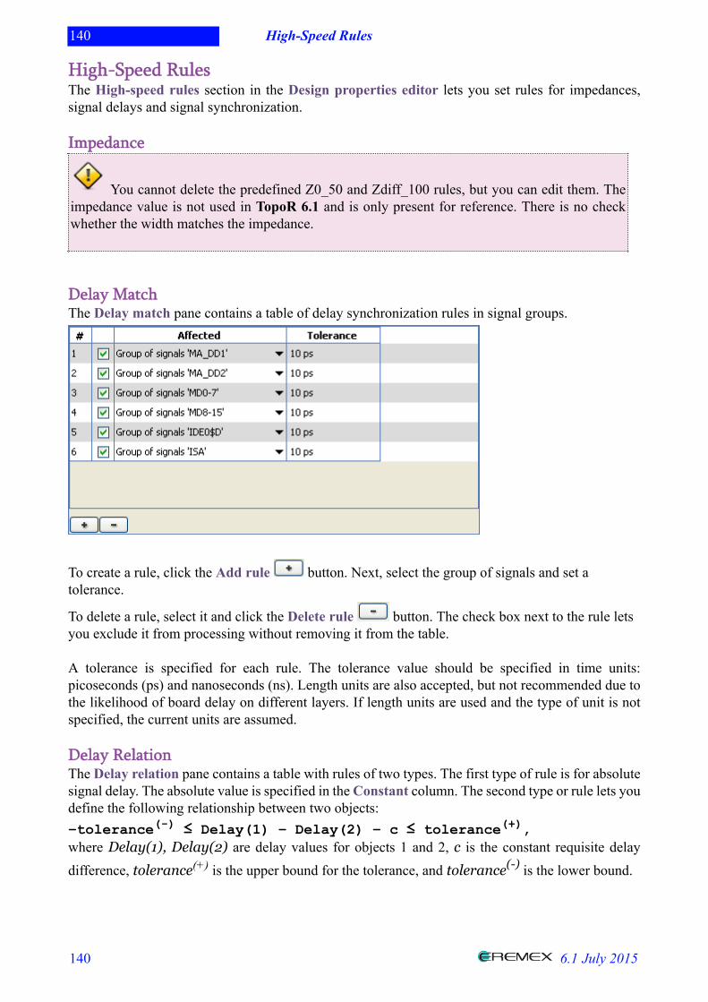
140 High-Speed Rules
140 6.1 July 2015
High-Speed RulesThe High-speed rules section in the Design properties editor lets you set rules for impedances,signal delays and signal synchronization.
Impedance
You cannot delete the predefined Z0_50 and Zdiff_100 rules, but you can edit them. Theimpedance value is not used in TopoR 6.1 and is only present for reference. There is no checkwhether the width matches the impedance.
Delay MatchThe Delay match pane contains a table of delay synchronization rules in signal groups.
To create a rule, click the Add rule button. Next, select the group of signals and set atolerance.
To delete a rule, select it and click the Delete rule button. The check box next to the rule letsyou exclude it from processing without removing it from the table.
A tolerance is specified for each rule. The tolerance value should be specified in time units:picoseconds (ps) and nanoseconds (ns). Length units are also accepted, but not recommended due tothe likelihood of board delay on different layers. If length units are used and the type of unit is notspecified, the current units are assumed.
Delay RelationThe Delay relation pane contains a table with rules of two types. The first type of rule is for absolutesignal delay. The absolute value is specified in the Constant column. The second type or rule lets youdefine the following relationship between two objects:–tolerance(-) ≤ Delay(1) – Delay(2) – c ≤ tolerance(+),where Delay(1), Delay(2) are delay values for objects 1 and 2, c is the constant requisite delaydifference, tolerance(+) is the upper bound for the tolerance, and tolerance(-) is the lower bound.
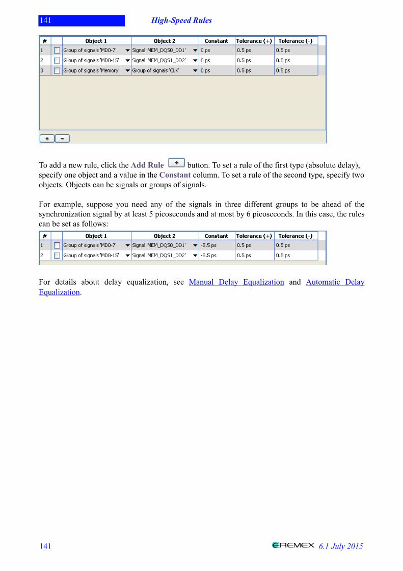
141 High-Speed Rules
141 6.1 July 2015
To add a new rule, click the Add Rule button. To set a rule of the first type (absolute delay),specify one object and a value in the Constant column. To set a rule of the second type, specify twoobjects. Objects can be signals or groups of signals.
For example, suppose you need any of the signals in three different groups to be ahead of thesynchronization signal by at least 5 picoseconds and at most by 6 picoseconds. In this case, the rulescan be set as follows:
For details about delay equalization, see Manual Delay Equalization and Automatic DelayEqualization.
142 Editing Techniques
142 6.1 July 2015
Editing TechniquesThis section describes:# Manual delay equalization# Automatic delay equalization# Routing differential pairs# Polygonal layout# Troubleshooting# FreeStyle mode# Refine tool# Via shifting# Inverting selected areas
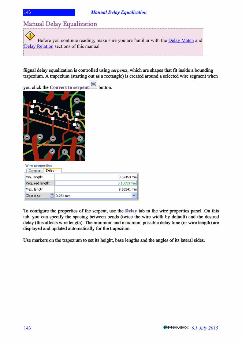
143 Manual Delay Equalization
143 6.1 July 2015
Manual Delay Equalization
Before you continue reading, make sure you are familiar with the Delay Match andDelay Relation sections of this manual.
Signal delay equalization is controlled using serpents, which are shapes that fit inside a boundingtrapezium. A trapezium (starting out as a rectangle) is created around a selected wire segment when
you click the Convert to serpent button.
To configure the properties of the serpent, use the Delay tab in the wire properties panel. On thistab, you can specify the spacing between bends (twice the wire width by default) and the desireddelay (this affects wire length). The minimum and maximum possible delay time (or wire length) aredisplayed and updated automatically for the trapezium.
Use markers on the trapezium to set its height, base lengths and the angles of its lateral sides.
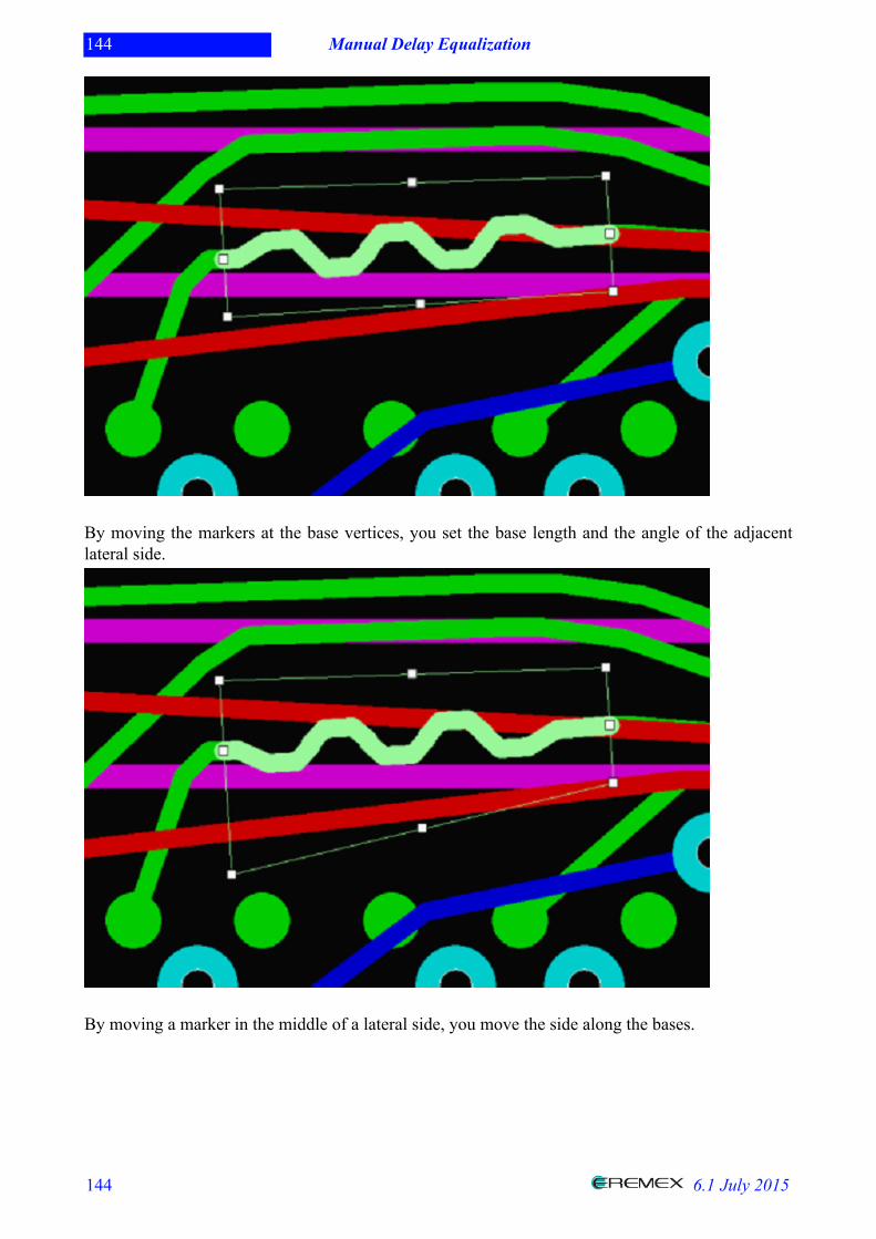
144 Manual Delay Equalization
144 6.1 July 2015
By moving the markers at the base vertices, you set the base length and the angle of the adjacentlateral side.
By moving a marker in the middle of a lateral side, you move the side along the bases.
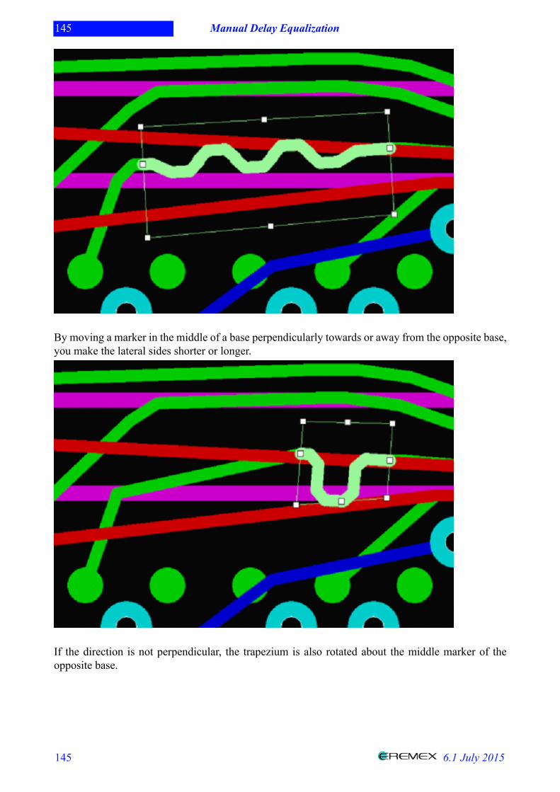
145 Manual Delay Equalization
145 6.1 July 2015
By moving a marker in the middle of a base perpendicularly towards or away from the opposite base,you make the lateral sides shorter or longer.
If the direction is not perpendicular, the trapezium is also rotated about the middle marker of theopposite base.
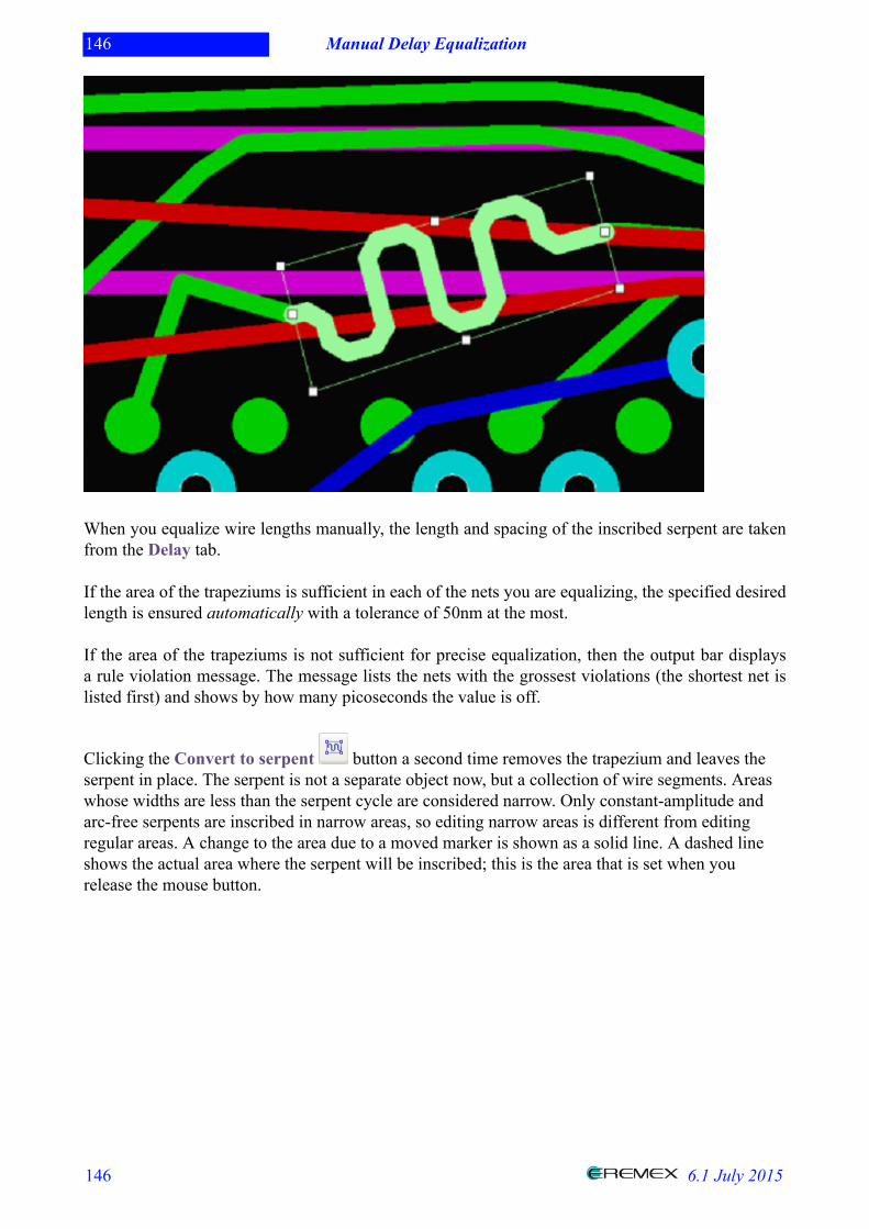
146 Manual Delay Equalization
146 6.1 July 2015
When you equalize wire lengths manually, the length and spacing of the inscribed serpent are takenfrom the Delay tab.
If the area of the trapeziums is sufficient in each of the nets you are equalizing, the specified desiredlength is ensured automatically with a tolerance of 50nm at the most.
If the area of the trapeziums is not sufficient for precise equalization, then the output bar displaysa rule violation message. The message lists the nets with the grossest violations (the shortest net islisted first) and shows by how many picoseconds the value is off.
Clicking the Convert to serpent button a second time removes the trapezium and leaves theserpent in place. The serpent is not a separate object now, but a collection of wire segments. Areaswhose widths are less than the serpent cycle are considered narrow. Only constant-amplitude andarc-free serpents are inscribed in narrow areas, so editing narrow areas is different from editingregular areas. A change to the area due to a moved marker is shown as a solid line. A dashed lineshows the actual area where the serpent will be inscribed; this is the area that is set when yourelease the mouse button.
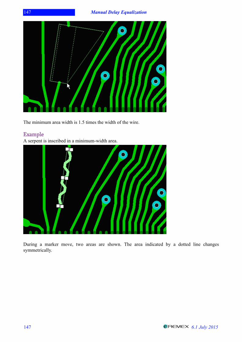
147 Manual Delay Equalization
147 6.1 July 2015
The minimum area width is 1.5 times the width of the wire.
ExampleA serpent is inscribed in a minimum-width area.
During a marker move, two areas are shown. The area indicated by a dotted line changessymmetrically.
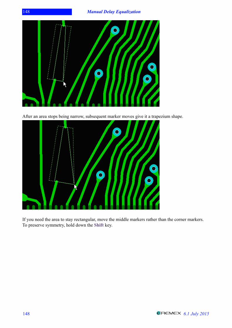
148 Manual Delay Equalization
148 6.1 July 2015
After an area stops being narrow, subsequent marker moves give it a trapezium shape.
If you need the area to stay rectangular, move the middle markers rather than the corner markers.To preserve symmetry, hold down the Shift key.
149 Automatic Delay Equalization
149 6.1 July 2015
Automatic Delay EqualizationThe Tools ► Create serpents menu item automatically adds serpents to wires that need equalization.When you equalize wire lengths automatically, the serpent has the specified length if there is enoughroom, or the maximum possible length if there is not enough room.
150 Routing Differential Pairs
150 6.1 July 2015
Routing Differential PairsTo route a differential pair, select Route ► Place diff pair in the main menu. Pads thatbelong to different differential pairs are highlighted in different colors.
A differential pair is a set of zipped and regular wires. Zipped wires are shown as a zipper with twosliders. A slider always stays perpendicular to the nearest segment of a zipped wire.
Clicking one of the highlighted pads creates a pair of wires at pads that are the specified distanceapart from each other. Clicking again places a slider under the cursor. From now on, the zipped wirepair is routed as a single wire.
When you approach another pair of pads, clicking one of them places a slider at the end of the lastsegment of the zipped wire and adds wires to connect the slider to the corresponding pads.
If you need to unzip the selected parts of a zipped wire pair, click the Unzip wires button. To zipthe wires of a differential pair, it is necessary to allocate parts of the segments that belong to thedifferential pair, for example, select a segment of one wire and hold down Ctrl then select anothersegment, then press X, after that click the Zip wires button in the toolbar.
To zip all differential pairs (for example, after autorouting) press Ctrl+A (select all), and then clickthe Zip wires button. This may result in some violations that need to be removed manually.
Requirements that wires need to meet to be zipped# The selected segments should belong to the wires that are part of the differential signalspecified in the rules.# The wires should be on the same layer.# The widths of the wires should observe the rule specified for the impedance.# The straight length of each of the wires must be no less than the width of the zipped wire pair(according to the rule for differential pairs that is twice the wire width plus clearance) multiplied bythree.
In the wire where the straight length of the selected segments is less than in the other wire,those selected segments are deleted, and a zipped pair replaces the longer selected segments ofthe other wire.
When you select a differential pair, the selected segment is highlighted. If the selected segment belongsto a zipped wire, then pressing the X key selects the zipped portion up to the slider. Pressing X againselects both wires in the differential pair, as shown in the following screenshots:
151 Routing Differential Pairs
151 6.1 July 2015
If the selected segment belongs to an unzipped wire, then pressing the X key selects the segment upto the slider. Pressing X again selects the entire wire, as shown in the following screenshots:
EditingEditing of selected segments of a zipped wire (moving segments, straightening selected parts) issimilar to editing regular wires. The widths of zipped wires can be modified only in Design ►Parameters ► High-Speed Rules ► Impedance.
When you delete a selected net (by pressing Delete), only unzipped portions are removed.
152 Routing Differential Pairs
152 6.1 July 2015
To switch layers, press the L key and select the next layer. As a result, a slider is automatically addedon the current layer, and a pair of vias is added on the new layer, as well as wire segments connectingthe vias and the corresponding slider pads.
To remove overlap between the wires of a differential pair, use the net swap feature. For that, in the
properties of the zipped wires, click the Swap Nets button, and then click Apply.
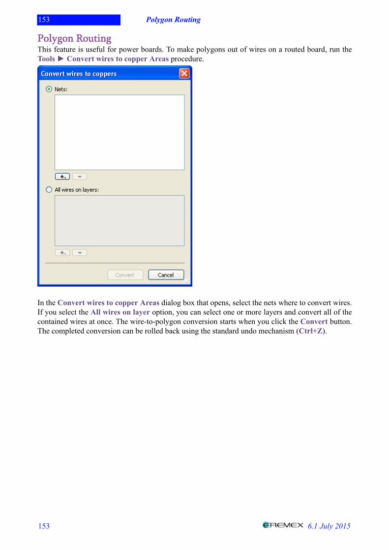
153 Polygon Routing
153 6.1 July 2015
Polygon RoutingThis feature is useful for power boards. To make polygons out of wires on a routed board, run theTools ► Convert wires to copper Areas procedure.
In the Convert wires to copper Areas dialog box that opens, select the nets where to convert wires.If you select the All wires on layer option, you can select one or more layers and convert all of thecontained wires at once. The wire-to-polygon conversion starts when you click the Convert button.The completed conversion can be rolled back using the standard undo mechanism (Ctrl+Z).
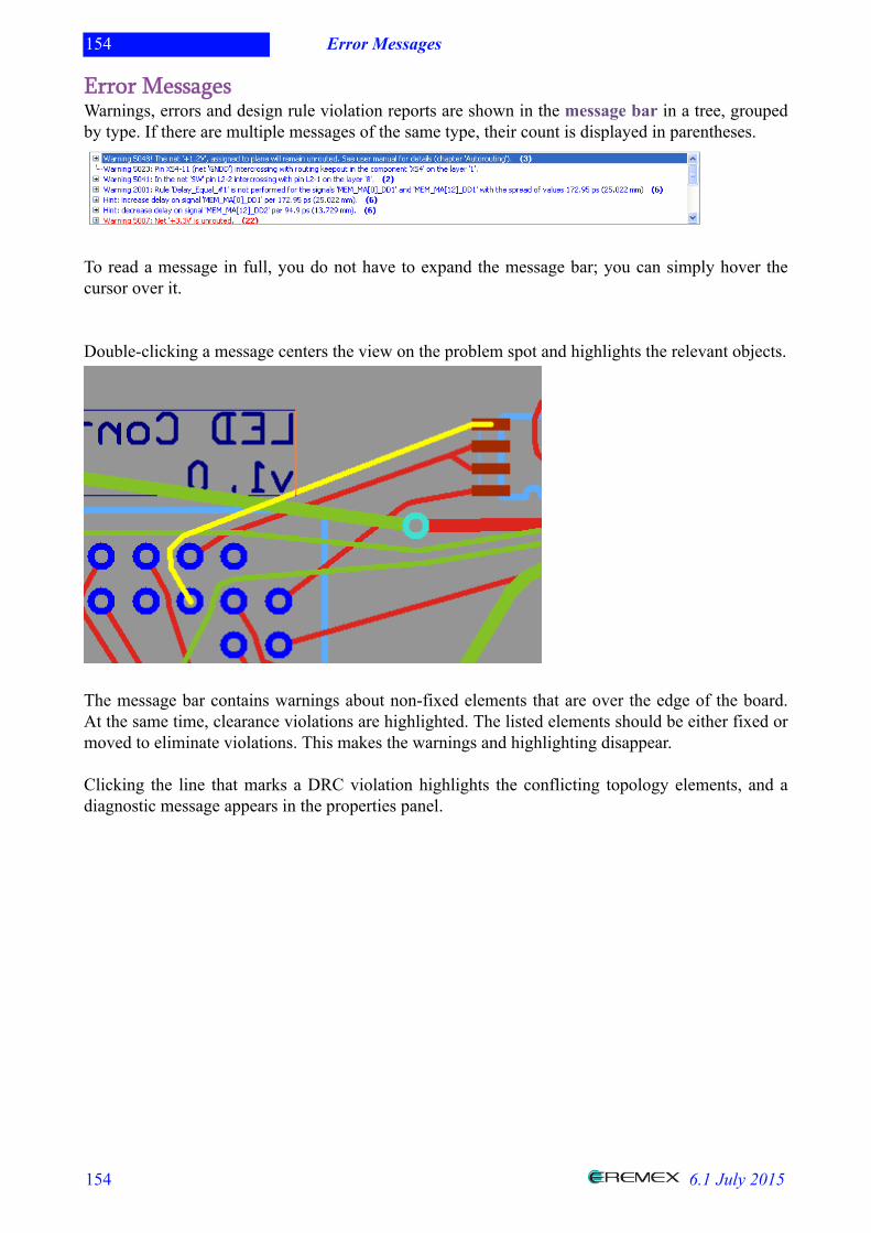
154 Error Messages
154 6.1 July 2015
Error MessagesWarnings, errors and design rule violation reports are shown in the message bar in a tree, groupedby type. If there are multiple messages of the same type, their count is displayed in parentheses.
To read a message in full, you do not have to expand the message bar; you can simply hover thecursor over it.
Double-clicking a message centers the view on the problem spot and highlights the relevant objects.
The message bar contains warnings about non-fixed elements that are over the edge of the board.At the same time, clearance violations are highlighted. The listed elements should be either fixed ormoved to eliminate violations. This makes the warnings and highlighting disappear.
Clicking the line that marks a DRC violation highlights the conflicting topology elements, and adiagnostic message appears in the properties panel.
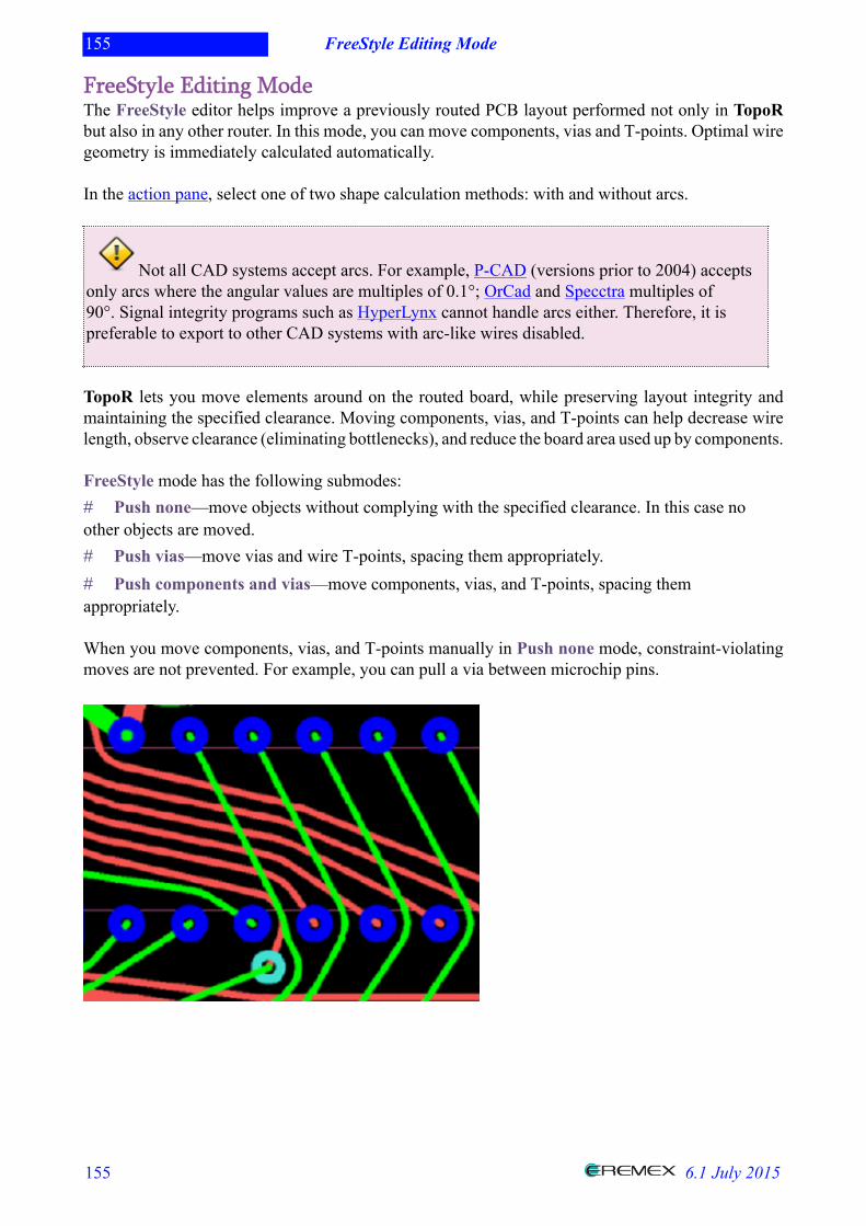
155 FreeStyle Editing Mode
155 6.1 July 2015
FreeStyle Editing ModeThe FreeStyle editor helps improve a previously routed PCB layout performed not only in TopoRbut also in any other router. In this mode, you can move components, vias and T-points. Optimal wiregeometry is immediately calculated automatically.
In the action pane, select one of two shape calculation methods: with and without arcs.
Not all CAD systems accept arcs. For example, P-CAD (versions prior to 2004) acceptsonly arcs where the angular values are multiples of 0.1°; OrCad and Specctra multiples of90°. Signal integrity programs such as HyperLynx cannot handle arcs either. Therefore, it ispreferable to export to other CAD systems with arc-like wires disabled.
TopoR lets you move elements around on the routed board, while preserving layout integrity andmaintaining the specified clearance. Moving components, vias, and T-points can help decrease wirelength, observe clearance (eliminating bottlenecks), and reduce the board area used up by components.
FreeStyle mode has the following submodes:# Push none—move objects without complying with the specified clearance. In this case noother objects are moved.# Push vias—move vias and wire T-points, spacing them appropriately.# Push components and vias—move components, vias, and T-points, spacing themappropriately.
When you move components, vias, and T-points manually in Push none mode, constraint-violatingmoves are not prevented. For example, you can pull a via between microchip pins.
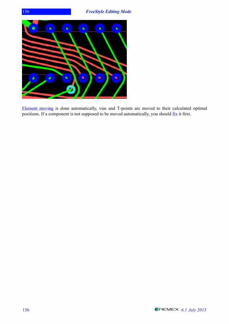
156 FreeStyle Editing Mode
156 6.1 July 2015
Element moving is done automatically, vias and T-points are moved to their calculated optimalpositions. If a component is not supposed to be moved automatically, you should fix it first.
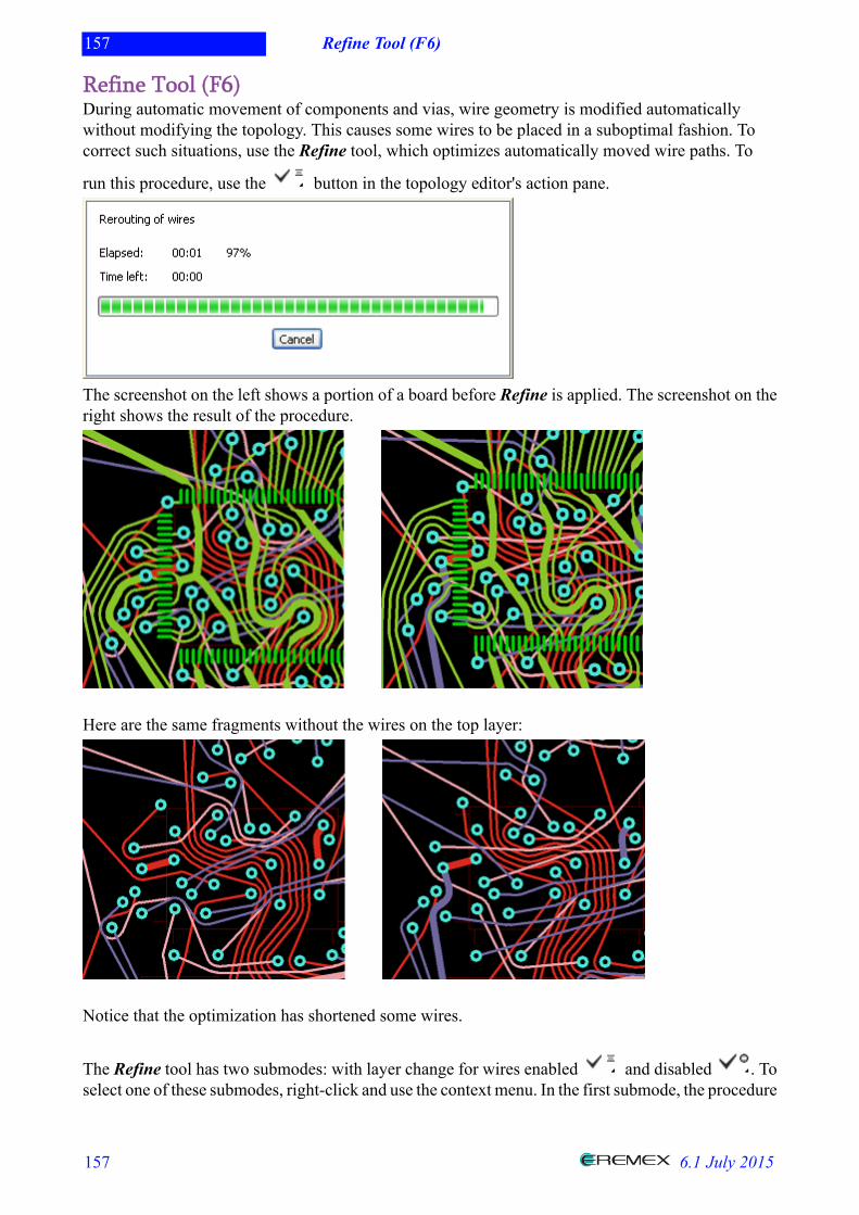
157 Refine Tool (F6)
157 6.1 July 2015
Refine Tool (F6)During automatic movement of components and vias, wire geometry is modified automaticallywithout modifying the topology. This causes some wires to be placed in a suboptimal fashion. Tocorrect such situations, use the Refine tool, which optimizes automatically moved wire paths. To
run this procedure, use the button in the topology editor's action pane.
The screenshot on the left shows a portion of a board before Refine is applied. The screenshot on theright shows the result of the procedure.
Here are the same fragments without the wires on the top layer:
Notice that the optimization has shortened some wires.
The Refine tool has two submodes: with layer change for wires enabled and disabled . Toselect one of these submodes, right-click and use the context menu. In the first submode, the procedure

158 Refine Tool (F6)
158 6.1 July 2015
can change not only the wire geometry but also its layer (if the wire connects through pads or vias). Insome cases, this decreases the number of vias. The Refine tool is most effective when designing multi-layered circuit boards. This use of the Refine tool is especially helpful in designing multi-layer boards
Redundant vias left behind by the Refine tool are deleted automatically.
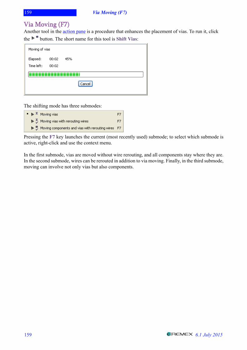
159 Via Moving (F7)
159 6.1 July 2015
Via Moving (F7)Another tool in the action pane is a procedure that enhances the placement of vias. To run it, clickthe button. The short name for this tool is Shift Vias:
The shifting mode has three submodes:
Pressing the F7 key launches the current (most recently used) submode; to select which submode isactive, right-click and use the context menu.
In the first submode, vias are moved without wire rerouting, and all components stay where they are.In the second submode, wires can be rerouted in addition to via moving. Finally, in the third submode,moving can involve not only vias but also components.
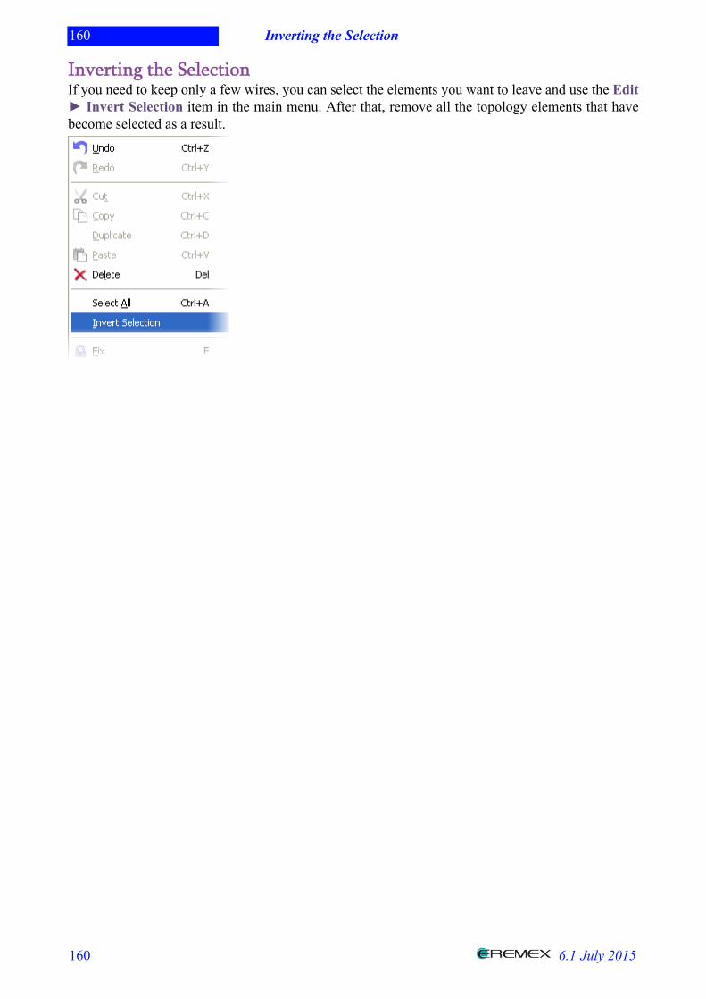
160 Inverting the Selection
160 6.1 July 2015
Inverting the SelectionIf you need to keep only a few wires, you can select the elements you want to leave and use the Edit► Invert Selection item in the main menu. After that, remove all the topology elements that havebecome selected as a result.

161 Data Recovery
161 6.1 July 2015
Data RecoveryTopoR automatically backs up data so that it can be subsequently recovered. Data is autosaved forevery project you open. When the project is closed normally, the backup data is deleted.
Autosaving of .fsx files is automatic (for any project that is open). Autosaving of routing data isenabled when you run autorouting and disabled when autorouting is completed.
Opening a Project after Abnormal TerminationIf you experience a program failure while working on a project, the next time you open the project,TopoR will check that the autosave file is more recent than the main project file. If this check confirmsabnormal termination, then notification is displayed.
Likewise, TopoR can notify you that you can recover autorouting data.
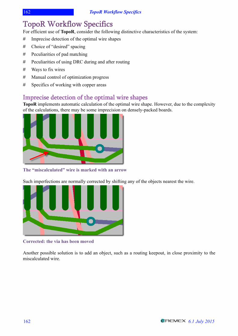
162 TopoR Workflow Specifics
162 6.1 July 2015
TopoR Workflow SpecificsFor efficient use of TopoR, consider the following distinctive characteristics of the system:# Imprecise detection of the optimal wire shapes# Choice of “desired” spacing# Peculiarities of pad matching# Peculiarities of using DRC during and after routing# Ways to fix wires# Manual control of optimization progress# Specifics of working with copper areas
Imprecise detection of the optimal wire shapesTopoR implements automatic calculation of the optimal wire shape. However, due to the complexityof the calculations, there may be some imprecision on densely-packed boards.
The “miscalculated” wire is marked with an arrow
Such imperfections are normally corrected by shifting any of the objects nearest the wire.
Corrected: the via has been moved
Another possible solution is to add an object, such as a routing keepout, in close proximity to themiscalculated wire.
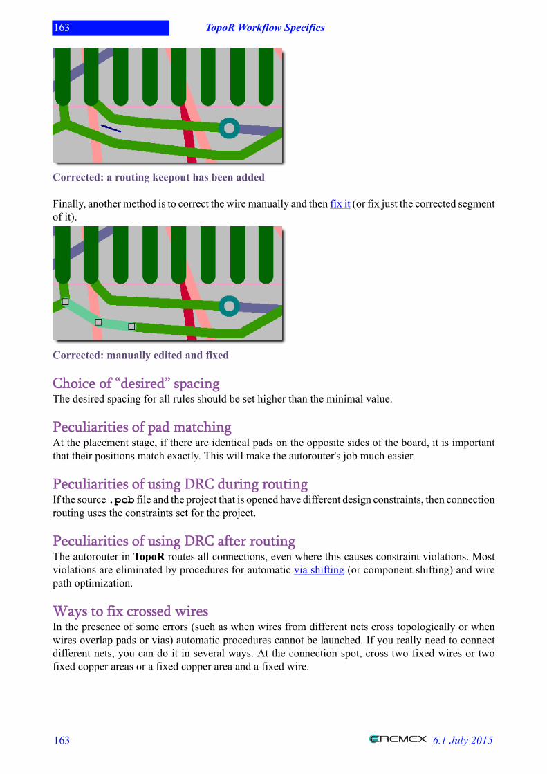
163 TopoR Workflow Specifics
163 6.1 July 2015
Corrected: a routing keepout has been added
Finally, another method is to correct the wire manually and then fix it (or fix just the corrected segmentof it).
Corrected: manually edited and fixed
Choice of “desired” spacingThe desired spacing for all rules should be set higher than the minimal value.
Peculiarities of pad matchingAt the placement stage, if there are identical pads on the opposite sides of the board, it is importantthat their positions match exactly. This will make the autorouter's job much easier.
Peculiarities of using DRC during routingIf the source .pcb file and the project that is opened have different design constraints, then connectionrouting uses the constraints set for the project.
Peculiarities of using DRC after routingThe autorouter in TopoR routes all connections, even where this causes constraint violations. Mostviolations are eliminated by procedures for automatic via shifting (or component shifting) and wirepath optimization.
Ways to fix crossed wiresIn the presence of some errors (such as when wires from different nets cross topologically or whenwires overlap pads or vias) automatic procedures cannot be launched. If you really need to connectdifferent nets, you can do it in several ways. At the connection spot, cross two fixed wires or twofixed copper areas or a fixed copper area and a fixed wire.
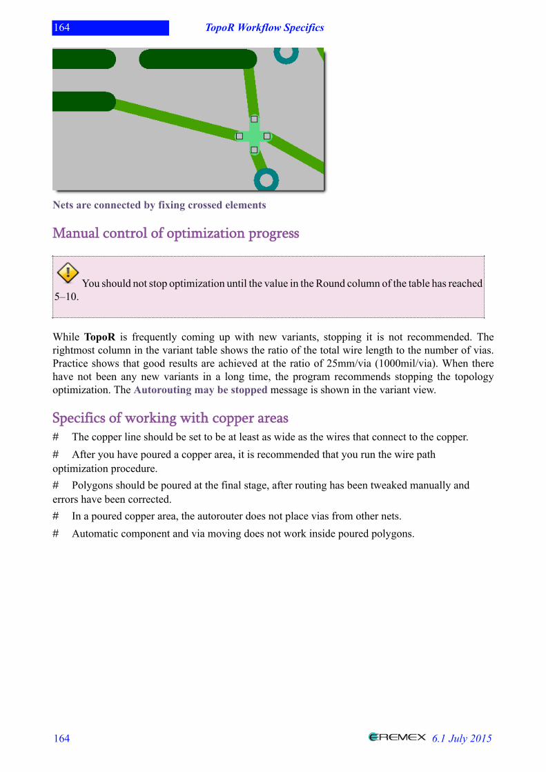
164 TopoR Workflow Specifics
164 6.1 July 2015
Nets are connected by fixing crossed elements
Manual control of optimization progress
You should not stop optimization until the value in the Round column of the table has reached5–10.
While TopoR is frequently coming up with new variants, stopping it is not recommended. Therightmost column in the variant table shows the ratio of the total wire length to the number of vias.Practice shows that good results are achieved at the ratio of 25mm/via (1000mil/via). When therehave not been any new variants in a long time, the program recommends stopping the topologyoptimization. The Autorouting may be stopped message is shown in the variant view.
Specifics of working with copper areas# The copper line should be set to be at least as wide as the wires that connect to the copper.# After you have poured a copper area, it is recommended that you run the wire pathoptimization procedure.# Polygons should be poured at the final stage, after routing has been tweaked manually anderrors have been corrected.# In a poured copper area, the autorouter does not place vias from other nets.# Automatic component and via moving does not work inside poured polygons.
165 Working with Other CAD Software
165 6.1 July 2015
Working with Other CAD SoftwareThis section describes the specifics of data interchange between TopoR and particular CAD systemsthrough file export and import. The term import is used to mean getting the output of other softwareinto TopoR, and export means the reverse.
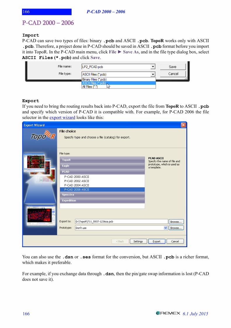
166 P-CAD 2000 – 2006
166 6.1 July 2015
P-CAD 2000 – 2006 ImportP-CAD can save two types of files: binary .pcb and ASCII .pcb. TopoR works only with ASCII.pcb. Therefore, a project done in P-CAD should be saved in ASCII .pcb format before you importit into TopoR. In the P-CAD main menu, click File ► Save As, and in the file type dialog box, selectASCII Files (*.pcb) and click Save.
ExportIf you need to bring the routing results back into P-CAD, export the file from TopoR to ASCII .pcband specify which version of P-CAD it is compatible with. For example, for P-CAD 2006 the fileselector in the export wizard looks like this:
You can also use the .dsn or .ses format for the conversion, but ASCII .pcb is a richer format,which makes it preferable.
For example, if you exchange data through .dsn, then the pin/gate swap information is lost (P-CADdoes not save it).
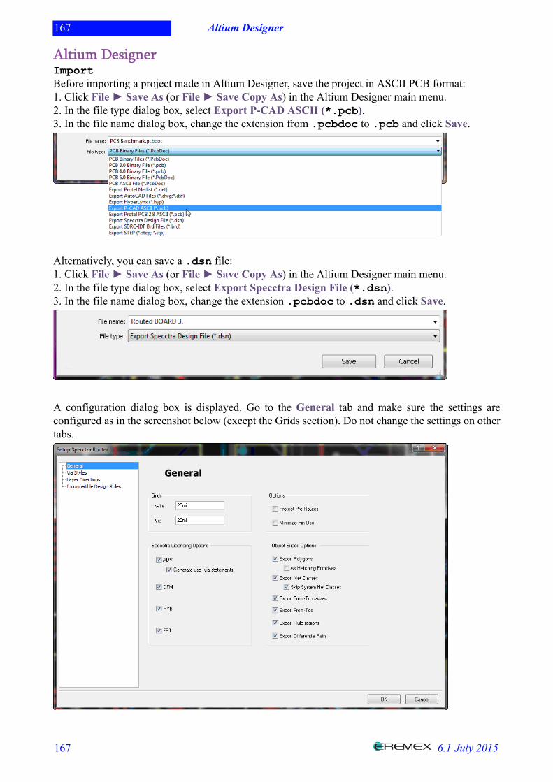
167 Altium Designer
167 6.1 July 2015
Altium DesignerImportBefore importing a project made in Altium Designer, save the project in ASCII PCB format:1. Click File ► Save As (or File ► Save Copy As) in the Altium Designer main menu.2. In the file type dialog box, select Export P-CAD ASCII (*.pcb).3. In the file name dialog box, change the extension from .pcbdoc to .pcb and click Save.
Alternatively, you can save a .dsn file:1. Click File ► Save As (or File ► Save Copy As) in the Altium Designer main menu.2. In the file type dialog box, select Export Specctra Design File (*.dsn).3. In the file name dialog box, change the extension .pcbdoc to .dsn and click Save.
A configuration dialog box is displayed. Go to the General tab and make sure the settings areconfigured as in the screenshot below (except the Grids section). Do not change the settings on othertabs.

168 Altium Designer
168 6.1 July 2015
The board outline should be drawn in Altium Designer using lines (arcs) on the Keep-out Layer,not specified as a room.
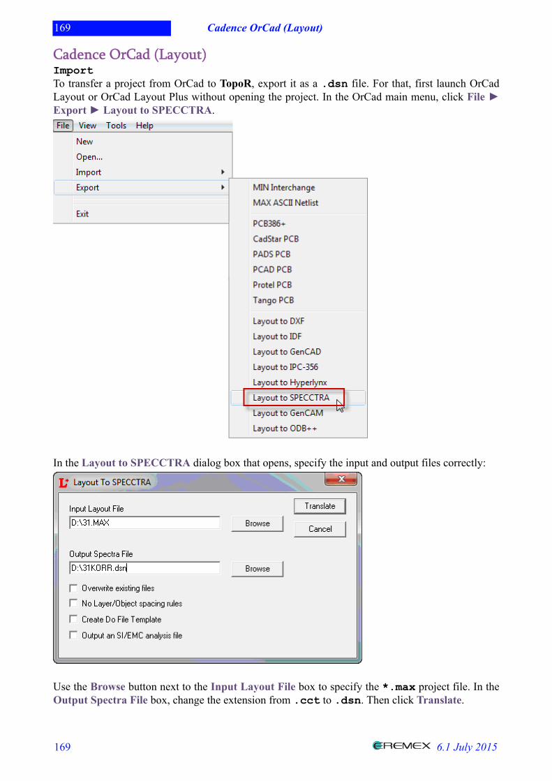
169 Cadence OrCad (Layout)
169 6.1 July 2015
Cadence OrCad (Layout)ImportTo transfer a project from OrCad to TopoR, export it as a .dsn file. For that, first launch OrCadLayout or OrCad Layout Plus without opening the project. In the OrCad main menu, click File ►Export ► Layout to SPECCTRA.
In the Layout to SPECCTRA dialog box that opens, specify the input and output files correctly:
Use the Browse button next to the Input Layout File box to specify the *.max project file. In theOutput Spectra File box, change the extension from .cct to .dsn. Then click Translate.
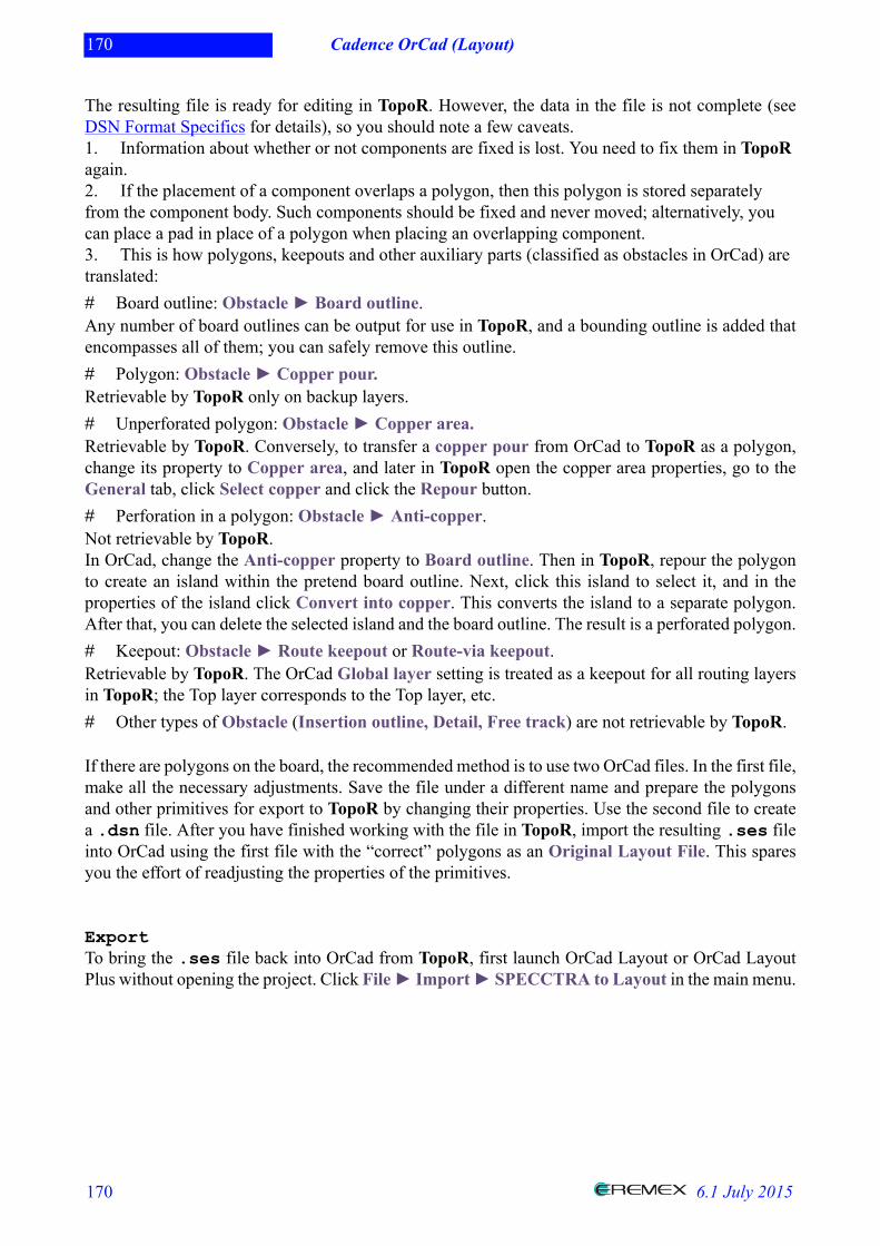
170 Cadence OrCad (Layout)
170 6.1 July 2015
The resulting file is ready for editing in TopoR. However, the data in the file is not complete (seeDSN Format Specifics for details), so you should note a few caveats.1. Information about whether or not components are fixed is lost. You need to fix them in TopoRagain.2. If the placement of a component overlaps a polygon, then this polygon is stored separatelyfrom the component body. Such components should be fixed and never moved; alternatively, youcan place a pad in place of a polygon when placing an overlapping component.3. This is how polygons, keepouts and other auxiliary parts (classified as obstacles in OrCad) aretranslated:# Board outline: Obstacle ► Board outline.Any number of board outlines can be output for use in TopoR, and a bounding outline is added thatencompasses all of them; you can safely remove this outline.# Polygon: Obstacle ► Copper pour.Retrievable by TopoR only on backup layers.# Unperforated polygon: Obstacle ► Copper area.Retrievable by TopoR. Conversely, to transfer a copper pour from OrCad to TopoR as a polygon,change its property to Copper area, and later in TopoR open the copper area properties, go to theGeneral tab, click Select copper and click the Repour button.# Perforation in a polygon: Obstacle ► Anti-copper.Not retrievable by TopoR.In OrCad, change the Anti-copper property to Board outline. Then in TopoR, repour the polygonto create an island within the pretend board outline. Next, click this island to select it, and in theproperties of the island click Convert into copper. This converts the island to a separate polygon.After that, you can delete the selected island and the board outline. The result is a perforated polygon.# Keepout: Obstacle ► Route keepout or Route-via keepout.Retrievable by TopoR. The OrCad Global layer setting is treated as a keepout for all routing layersin TopoR; the Top layer corresponds to the Top layer, etc.# Other types of Obstacle (Insertion outline, Detail, Free track) are not retrievable by TopoR.
If there are polygons on the board, the recommended method is to use two OrCad files. In the first file,make all the necessary adjustments. Save the file under a different name and prepare the polygonsand other primitives for export to TopoR by changing their properties. Use the second file to createa .dsn file. After you have finished working with the file in TopoR, import the resulting .ses fileinto OrCad using the first file with the “correct” polygons as an Original Layout File. This sparesyou the effort of readjusting the properties of the primitives.
ExportTo bring the .ses file back into OrCad from TopoR, first launch OrCad Layout or OrCad LayoutPlus without opening the project. Click File ► Import ► SPECCTRA to Layout in the main menu.
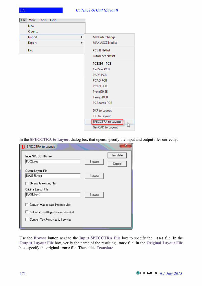
171 Cadence OrCad (Layout)
171 6.1 July 2015
In the SPECCTRA to Layout dialog box that opens, specify the input and output files correctly:
Use the Browse button next to the Input SPECCTRA File box to specify the .ses file. In theOutput Layout File box, verify the name of the resulting .max file. In the Original Layout Filebox, specify the original .max file. Then click Translate.
172 Cadence OrCad (Layout)
172 6.1 July 2015
Some information is not written to the .ses file, so certain changes are not retrievable by OrCad.The following data cannot be retrieved:1. Newly created layers. OrCad will lose the wires routed on such layers2. Board layout changes.3. Changes to pads and vias (or addition of new types).4. Via matrices created in TopoR. In fact, the matrix is written to the .ses file, but OrCaddeletes all vias but one as duplicates. You have the option to create this matrix in OrCad using theFree Via feature. TopoR treats such vias as single-component FreePads and makes sure they are notlost in conversion.
InterchangeWhen creating a library in OrCad, pay attention to pad coordinates (or verify them in the project).Even though OrCad lets you have five or more decimal places in coordinate values, you should notuse more than four digits after the decimal point, because that is the precision used in TopoR. Ifthere are five or more digits (a zero in the fifth decimal place is acceptable), a rounding error willoccur during data transfer into OrCad after routing in TopoR. OrCad will consider some of the netsunrouted, even though they may be routed. You should not ignore such errors, because you mightmiss an actual unrouted net. In addition, if you export the project for adjustments in TopoR, all of the“unrouted” wires will not be written to the .dsn file and will be lost.
To check and correct pad coordinates in an existing OrCad project, consider using the Tool ►Footprint ► Select from Spreadsheet menu item. Before this, make sure precision is configuredcorrectly: In Options ► System Settings, the Display Resolution option should be set to 0.00001.Otherwise, fewer decimal places may be displayed than there really are.
Other considerations:
1. Do not use Russian characters and spaces in file names (OrCad will fail to read them). 2. When files are converted back and forth, net width and clearance need to be reconfiguredin TopoR. Therefore, you should configure them in OrCad in the first place. To specify netclearance, go to Options ►Global Spacing. The clearance set there will be treated as minimalby TopoR. For the nominal clearance, either leave the value set automatically by TopoR, orchange it if necessary. Different clearance values are supported for different board layers (thiscan be configured in OrCad). To specify net width, go to View Spreadsheet ►Nets. The ConnWeight value is used. TopoR will build nets by group and set a width for each group. This netwidth value will be treated as minimal in TopoR. 3. If a pad is not connected to any net in an OrCad design, then a keepout for all layers iswritten to the .dsn file in its place. The diameter of the keepout is equal to the diameter of thepad. TopoR shows online DRC errors in such areas, but final DRC shows no errors. You caneither ignore such errors or select the keepout outline (it is obstructed by the pad) and delete it.
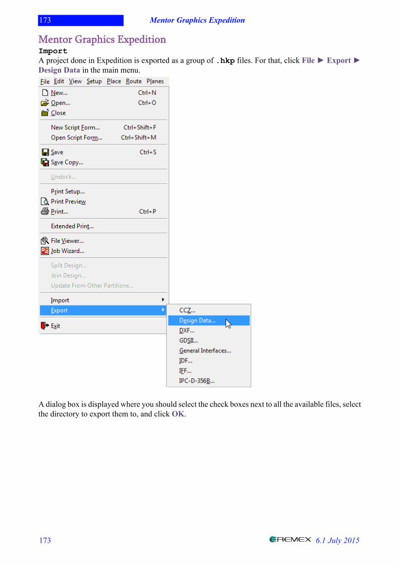
173 Mentor Graphics Expedition
173 6.1 July 2015
Mentor Graphics ExpeditionImportA project done in Expedition is exported as a group of .hkp files. For that, click File ► Export ►Design Data in the main menu.
A dialog box is displayed where you should select the check boxes next to all the available files, selectthe directory to export them to, and click OK.
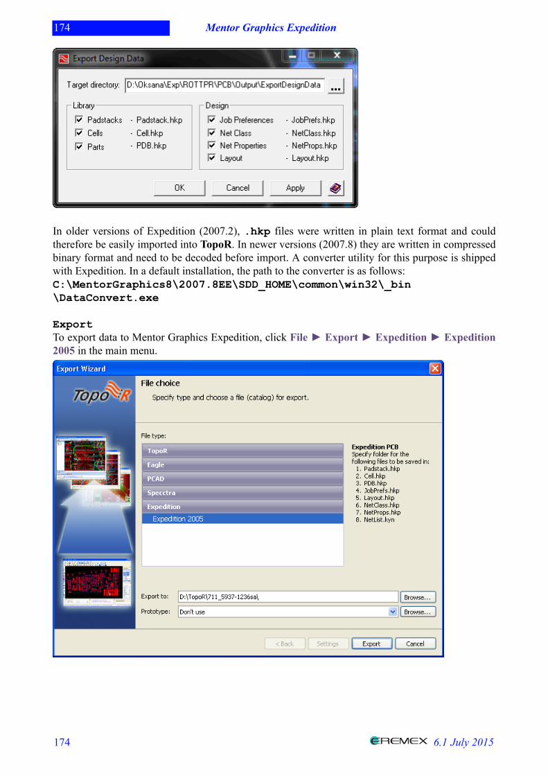
174 Mentor Graphics Expedition
174 6.1 July 2015
In older versions of Expedition (2007.2), .hkp files were written in plain text format and couldtherefore be easily imported into TopoR. In newer versions (2007.8) they are written in compressedbinary format and need to be decoded before import. A converter utility for this purpose is shippedwith Expedition. In a default installation, the path to the converter is as follows:C:\MentorGraphics8\2007.8EE\SDD_HOME\common\win32\_bin\DataConvert.exe
ExportTo export data to Mentor Graphics Expedition, click File ► Export ► Expedition ► Expedition2005 in the main menu.

175 Mentor Graphics Expedition
175 6.1 July 2015
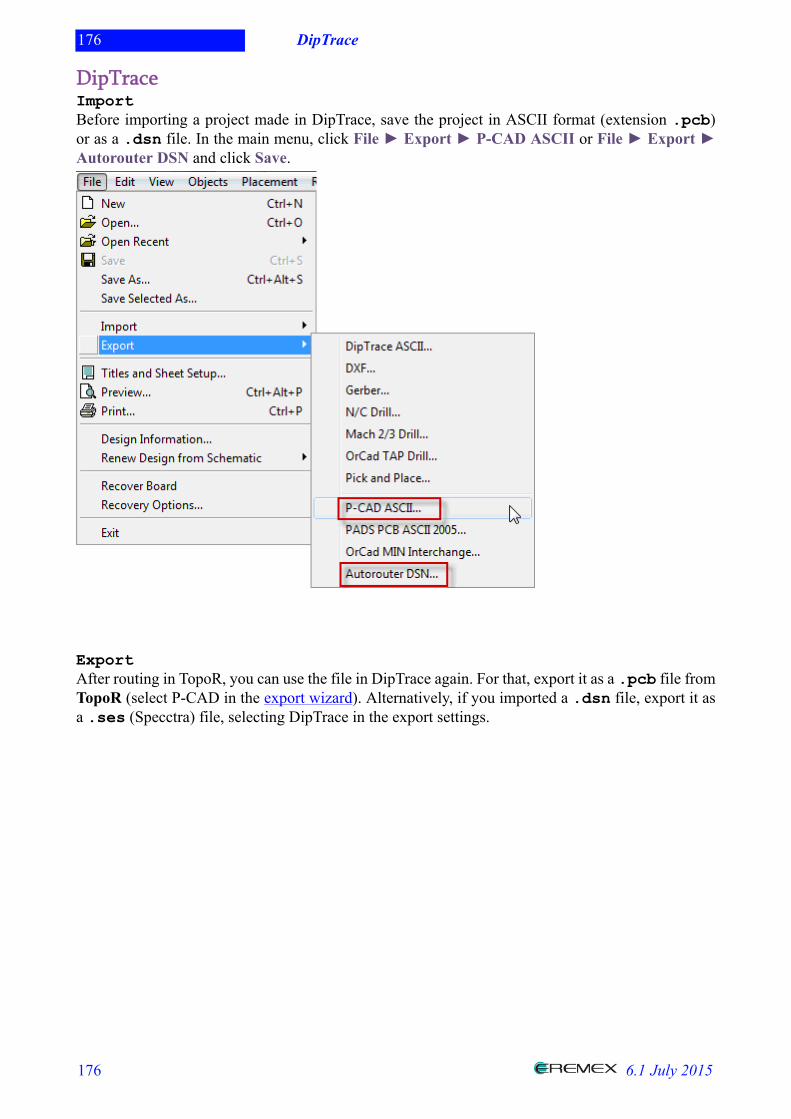
176 DipTrace
176 6.1 July 2015
DipTraceImportBefore importing a project made in DipTrace, save the project in ASCII format (extension .pcb)or as a .dsn file. In the main menu, click File ► Export ► P-CAD ASCII or File ► Export ►Autorouter DSN and click Save.
ExportAfter routing in TopoR, you can use the file in DipTrace again. For that, export it as a .pcb file fromTopoR (select P-CAD in the export wizard). Alternatively, if you imported a .dsn file, export it asa .ses (Specctra) file, selecting DipTrace in the export settings.
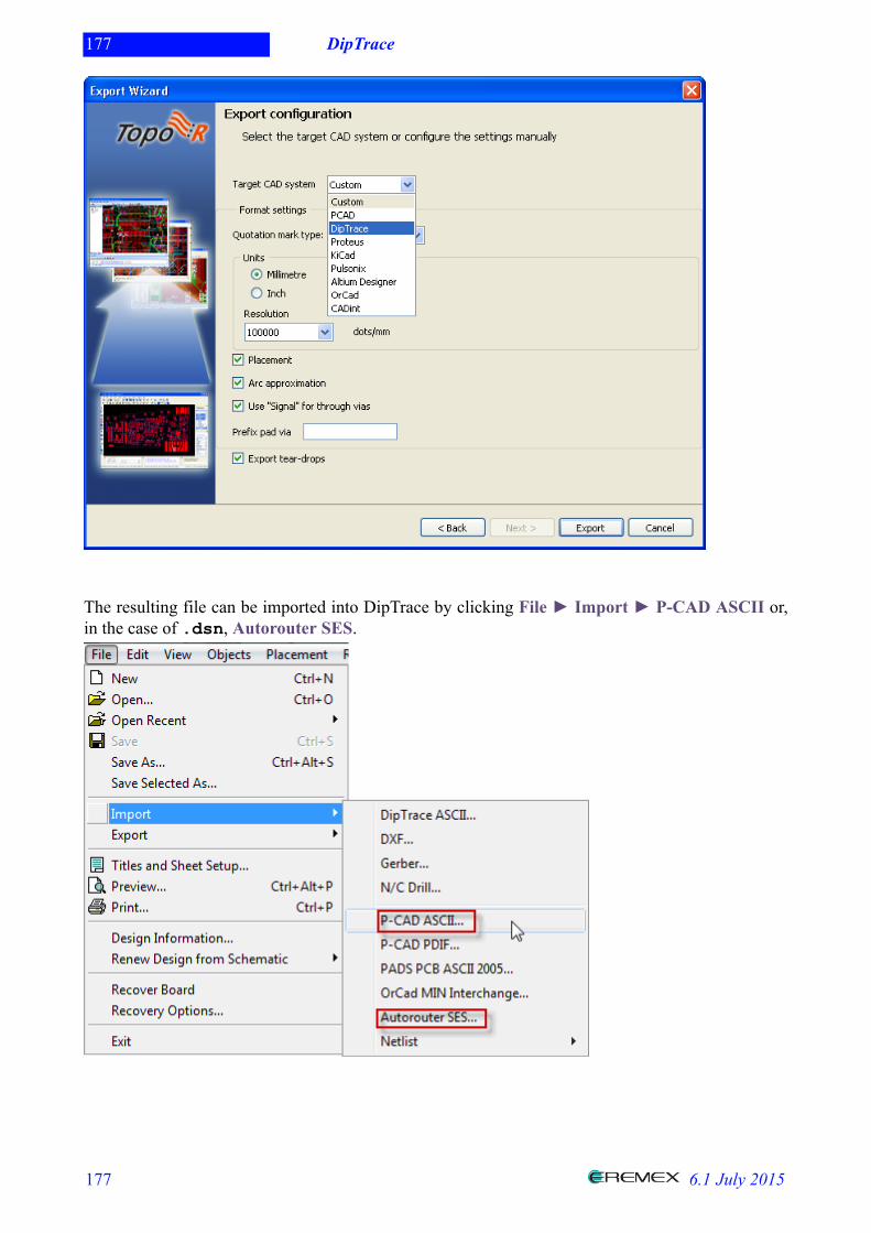
177 DipTrace
177 6.1 July 2015
The resulting file can be imported into DipTrace by clicking File ► Import ► P-CAD ASCII or,in the case of .dsn, Autorouter SES.

178 DipTrace
178 6.1 July 2015
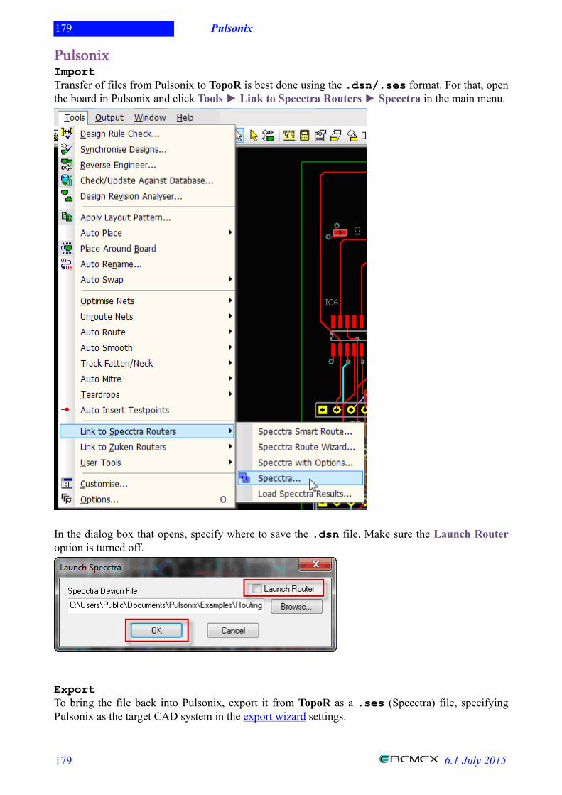
179 Pulsonix
179 6.1 July 2015
PulsonixImportTransfer of files from Pulsonix to TopoR is best done using the .dsn/.ses format. For that, openthe board in Pulsonix and click Tools ► Link to Specctra Routers ► Specctra in the main menu.
In the dialog box that opens, specify where to save the .dsn file. Make sure the Launch Routeroption is turned off.
ExportTo bring the file back into Pulsonix, export it from TopoR as a .ses (Specctra) file, specifyingPulsonix as the target CAD system in the export wizard settings.
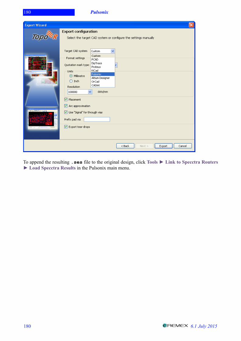
180 Pulsonix
180 6.1 July 2015
To append the resulting .ses file to the original design, click Tools ► Link to Specctra Routers► Load Specctra Results in the Pulsonix main menu.
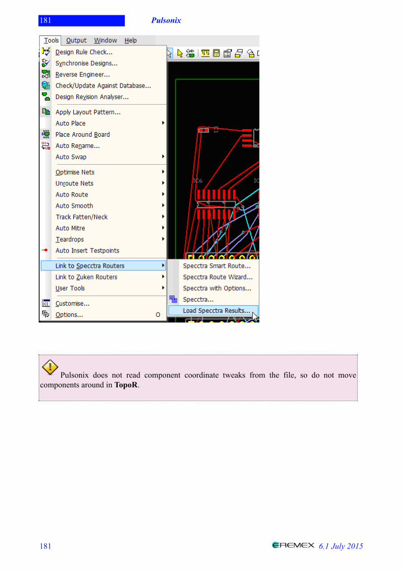
181 Pulsonix
181 6.1 July 2015
Pulsonix does not read component coordinate tweaks from the file, so do not movecomponents around in TopoR.
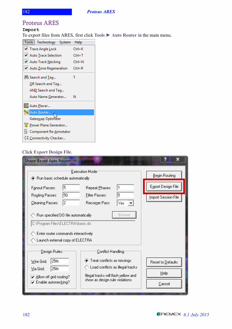
182 Proteus ARES
182 6.1 July 2015
Proteus ARESImportTo export files from ARES, first click Tools ► Auto Router in the main menu.
Click Export Design File.
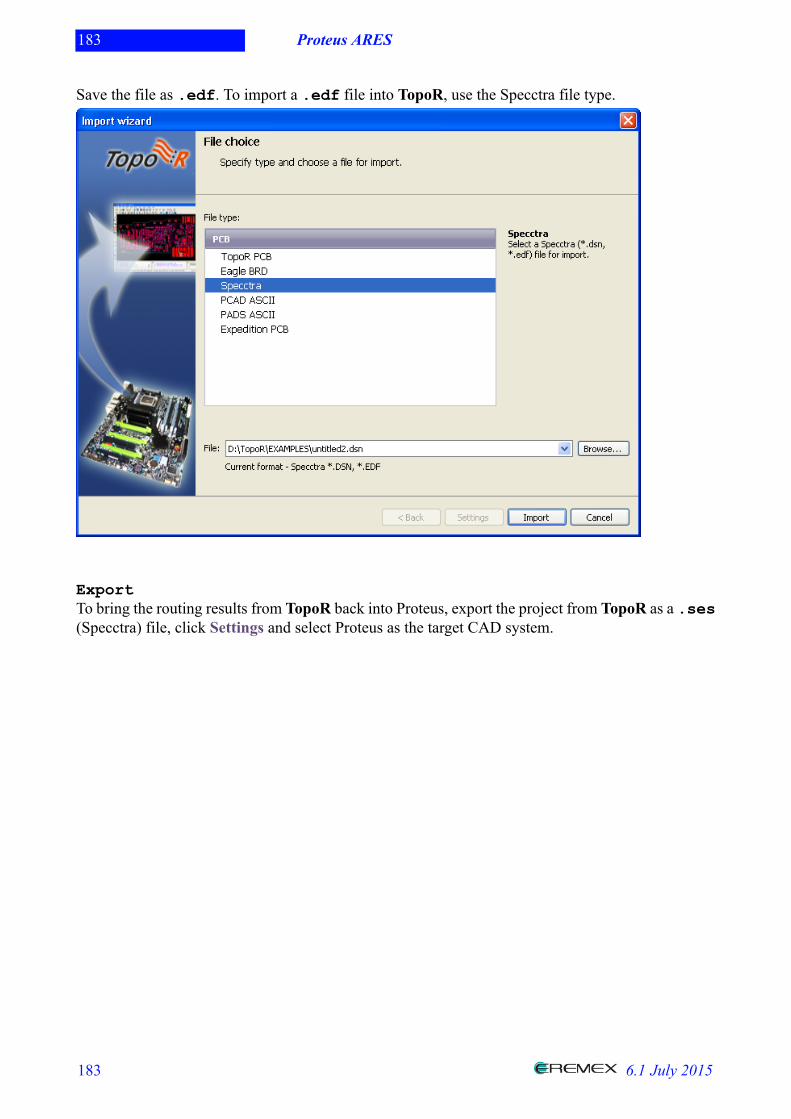
183 Proteus ARES
183 6.1 July 2015
Save the file as .edf. To import a .edf file into TopoR, use the Specctra file type.
ExportTo bring the routing results from TopoR back into Proteus, export the project from TopoR as a .ses(Specctra) file, click Settings and select Proteus as the target CAD system.
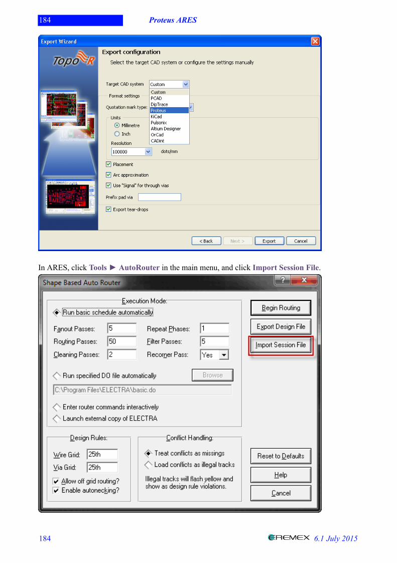
184 Proteus ARES
184 6.1 July 2015
In ARES, click Tools ► AutoRouter in the main menu, and click Import Session File.
185 Proteus ARES
185 6.1 July 2015
Load the .ses file.
Proteus does not read component coordinate tweaks from the .ses file, so do not movecomponents around in TopoR.
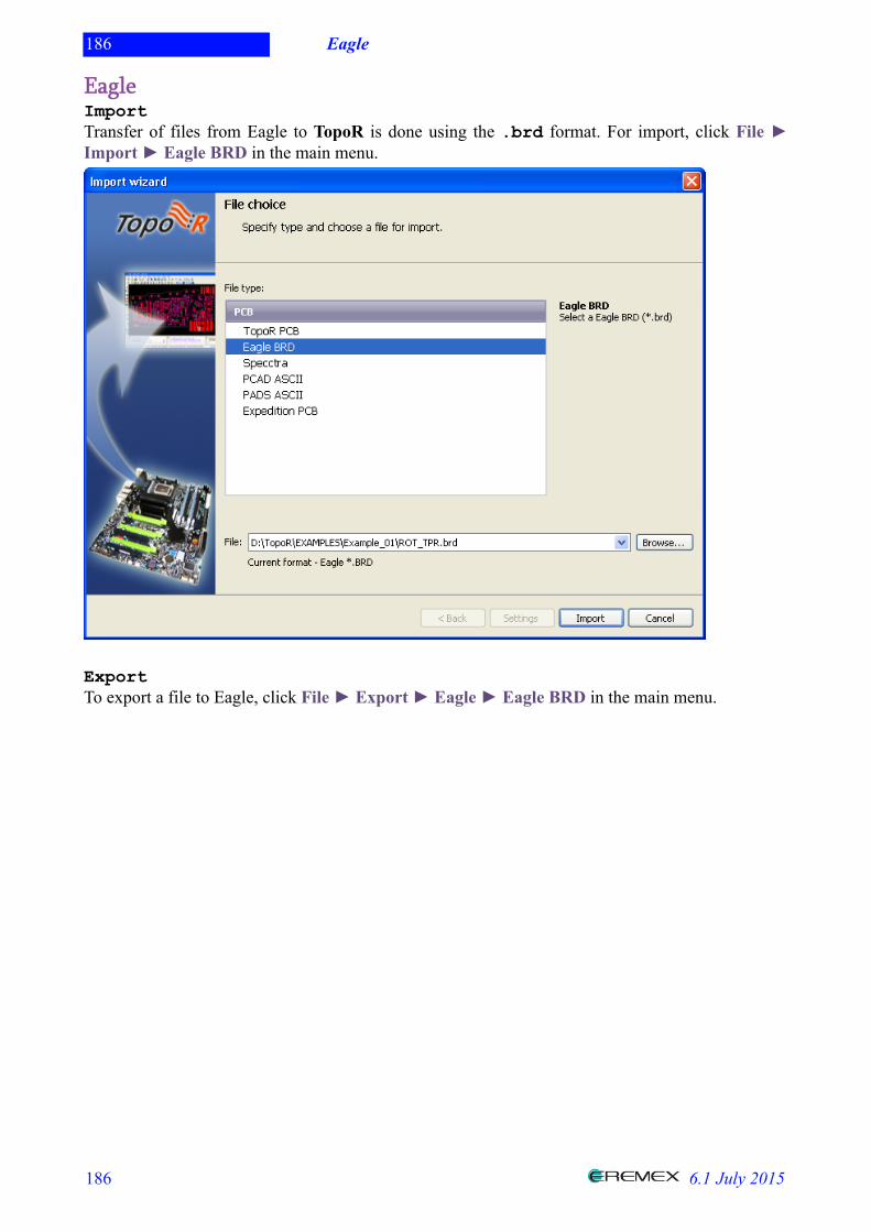
186 Eagle
186 6.1 July 2015
EagleImportTransfer of files from Eagle to TopoR is done using the .brd format. For import, click File ►Import ► Eagle BRD in the main menu.
ExportTo export a file to Eagle, click File ► Export ► Eagle ► Eagle BRD in the main menu.
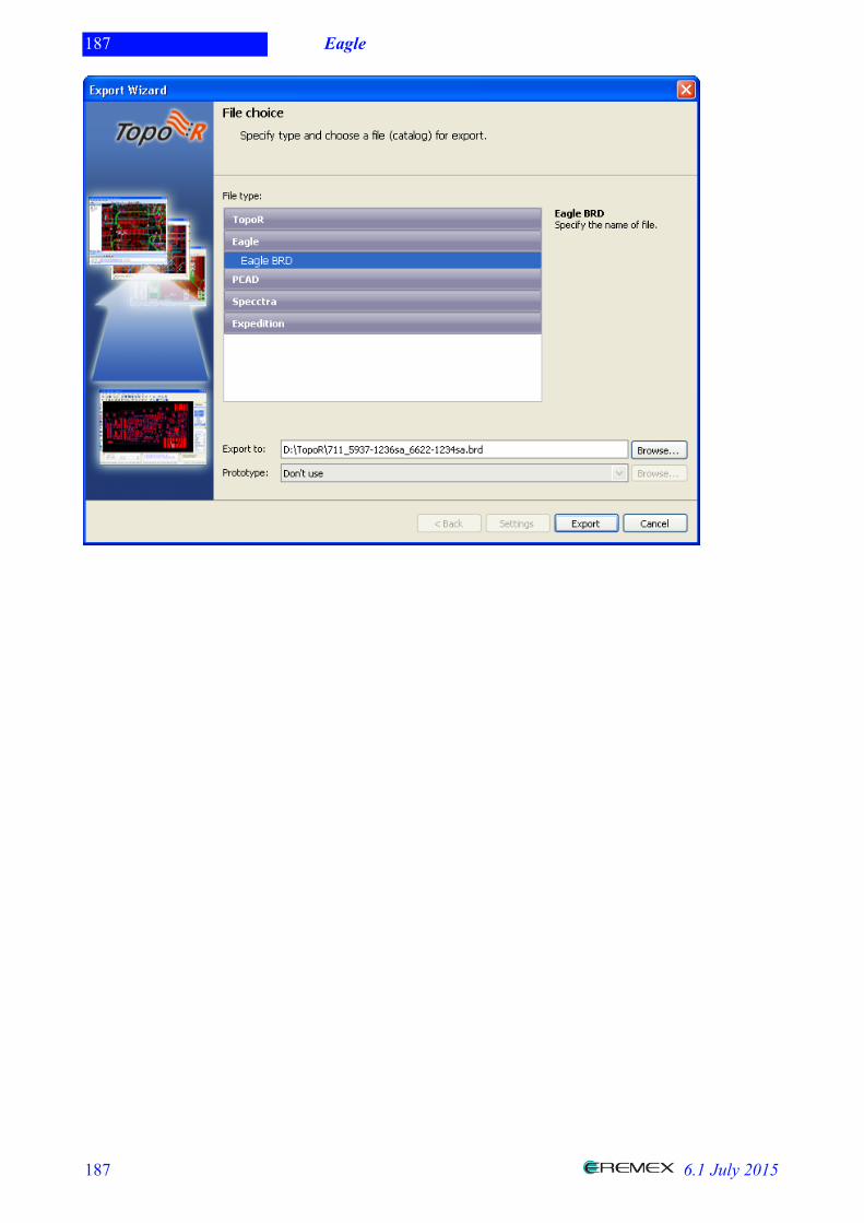
187 Eagle
187 6.1 July 2015
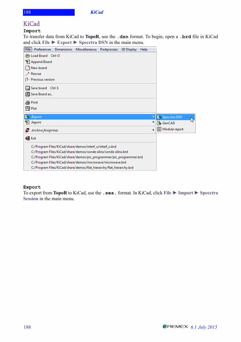
188 KiCad
188 6.1 July 2015
KiCadImportTo transfer data from KiCad to TopoR, use the .dsn format. To begin, open a .brd file in KiCadand click File ► Export ► Specctra DSN in the main menu.
ExportTo export from TopoR to KiCad, use the .ses. format. In KiCad, click File ► Import ► SpecctraSession in the main menu.
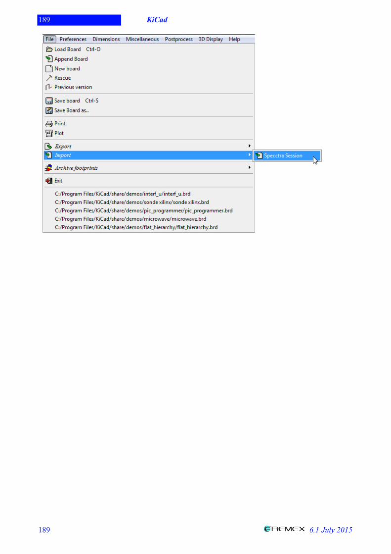
189 KiCad
189 6.1 July 2015
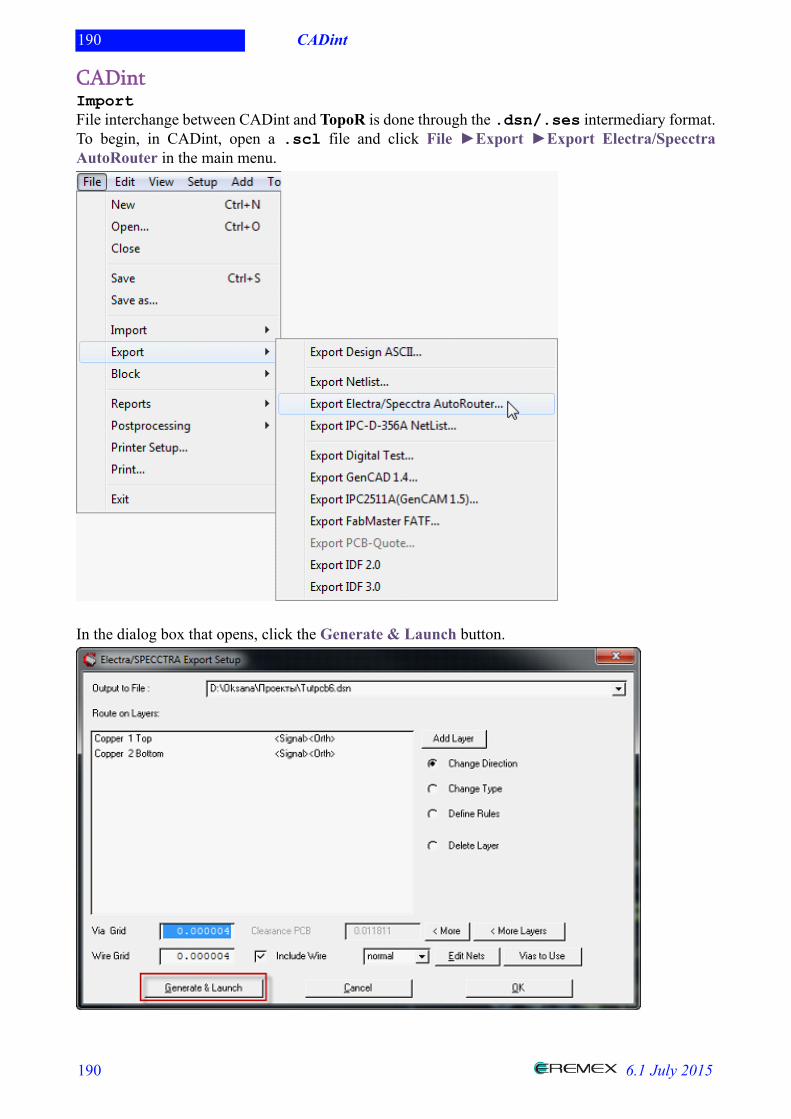
190 CADint
190 6.1 July 2015
CADintImportFile interchange between CADint and TopoR is done through the .dsn/.ses intermediary format.To begin, in CADint, open a .scl file and click File ►Export ►Export Electra/SpecctraAutoRouter in the main menu.
In the dialog box that opens, click the Generate & Launch button.
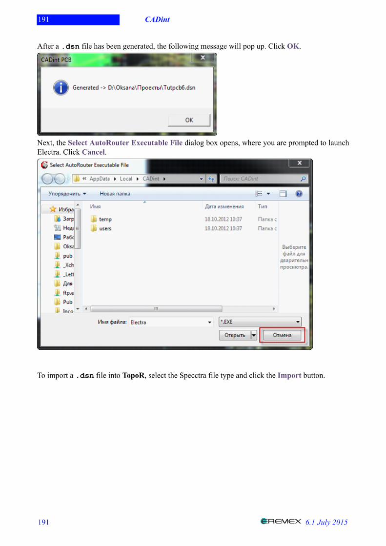
191 CADint
191 6.1 July 2015
After a .dsn file has been generated, the following message will pop up. Click OK.
Next, the Select AutoRouter Executable File dialog box opens, where you are prompted to launchElectra. Click Cancel.
To import a .dsn file into TopoR, select the Specctra file type and click the Import button.
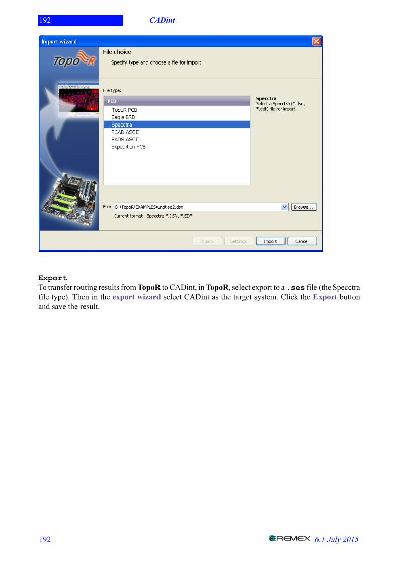
192 CADint
192 6.1 July 2015
ExportTo transfer routing results from TopoR to CADint, in TopoR, select export to a .ses file (the Specctrafile type). Then in the export wizard select CADint as the target system. Click the Export buttonand save the result.
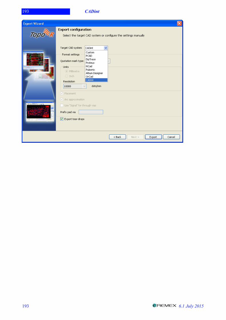
193 CADint
193 6.1 July 2015
194 DSN Format Specifics
194 6.1 July 2015
DSN Format SpecificsThe DSN format was designed for data exchange with the Specctra router and has a number oflimitations:
1. The via diameter is not defined. (TopoR sets the default via diameters.)
If you are planning to output .dxf or Gerber files from TopoR, you should configure thevia diameter in advance.
2. Information about mask and paste layers is not defined.
If you are planning to output Gerber files from TopoR, you should create such layers andprimitives on them in advance.
3. Text is not stored, but the bounding rectangle around it is preserved, defined as a keepout.
This is sufficient for correct routing, but the text contents cannot be edited.
4. Component labels must not contain apostrophes (') or quotation marks ("), because one of thesecharacters is reserved for special uses (either one, depending on to the CAD system that writes the.dsn) and will not be parsed. This can cause duplicate component names and other problems.
195 D. Reference
195 6.1 July 2015
D. ReferenceThe sections in part D contain useful tips, FAQs, button and default hotkey lists, an index spanning allof this manual, general operation recommendations and a detailed example of designing a relativelysimple printed circuit board.
196 Useful Tips
196 6.1 July 2015
Useful TipsBefore you start, consider creating a working directory for the project and put the original file in it.This will make the program save the project file and intermediary result files in the same directory,which makes it easier to find files.
It is difficult to achieve good results with an initial component layout where no routing has been done.Normally, the process of component placement and routing involves several stages, as follows:
1. Initial component placement.2. Connection routing.3. Detection of areas with excessively dense wire and via patterns.4. Changes to component placement.5. A new iteration of connection routing.
And so on, until the required result is attained.

197 Frequently Asked Questions
197 6.1 July 2015
Frequently Asked QuestionsGeneral Information about TopoRIs TopoR like other PCB design software? Will experience with other CAD software help melearn TopoR faster?TopoR is fundamentally different from other CAD software. It's possible that knowledge of anotherCAD system may even slow you down.
How complex are the boards I can lay out in TopoR?The current TopoR configurations can lay out boards with up to 32 routing layers.
Who uses TopoR today? Are there any problems in production?The software is used successfully in businesses and higher education institutions in Russia (from St.Petersburg to Petropavlovsk-Kamchatsky), the Ukraine (Kiev, Kharkiv, Zhytomyr, Severodonetsk,Vinnytsia, Odessa), India (Heydarabad, Ahmedabad, Haryana), and also in the USA, Kazakhstan,Macedonia and other countries.
Purchasing, Support, LearningIs there a network license for the software? How many workstations is it valid for?If you buy five or more licenses, you get a network key without any additional payment.
The documentation is insufficient for me; how else can I learn to work in TopoR?The easiest way is to ask any questions that arise on the forum or send them to the addresses listedin the Contacts section of the website: http://www.eremex.com. In the Tutorials section you can findshort educational videos. In addition, we can offer instruction in learning centers in St. Petersburg andMoscow. You only need to fill out an application form.
What kind of technical support do I receive after purchase?Within one year of purchasing a version of the software, you will get all updates free of charge. Youcan take a free course in a learning center in St. Petersburg or Moscow. Online support will prioritizeyour requests higher than those from demo version users.
How long is the software license valid?The license never expires.
System RequirementsWhat are the minimal hardware and software requirements for running TopoR?# PC-compatible computer with an Intel® Pentium® III 1000 MHz CPU# Operating system: Microsoft® Windows® 2000 (SP3), XP (SP2 or SP3), Vista, Windows 7,Windows 8# Microsoft® Internet Explorer 5.0# Windows Installer 3.0 or higher# RAM: 512MB.# 100MB hard disk space# SVGA monitor and graphics adapter, 256 colors, 1024x768.# Mouse with a scroll wheel
198 Frequently Asked Questions
198 6.1 July 2015
Can I use other OSs, such as Linux or UNIX?Currently, you can run only the Lite version in Wine. Support for Linux in TopoR is planned.
Import and ExportCan I work in TopoR exclusively, without using other CAD software?No. At this time, TopoR does not implement a comprehensive design cycle, although developmentin this area is ongoing.
Data from what CAD systems can be transferred to TopoR?# P-CAD 2000-2006—through the ASCII PCB format# Altium Designer—through the ASCII PCB format# Cadence OrCad—through the .dsn format# Mentor Graphics Expedition—through .hkp files# Mentor Graphics PADS—PADS ASCII PCB (for versions from PowerPCB V3.5 to PADSLayout V2005.2)# DipTrace—through the ASCII PCB format# Proteus ARES—through the .dsn (.edf) format# Eagle—through the .brd and .dsn formats# KiCad—through the .dsn format# CADint—through the .dsn format# Pulsonix—through the .dsn format
Can I export the project I make in TopoR to other CAD software?Yes. The program supports import and export of the following file formats:# PCAD ASCII PCB versions 2000, 2002, 2004, 2006# PADS ASCII PCB versions 3.5, 4.0, 5.0, 2005.0# DSN/SES (SPECCTRA, Electra)In addition, DXF output is possible for interchange with mechanical CAD software and GERBERand DRILL output for putting boards in production.
The documentation says that the signal data I add can be lost during export to other CADsoftware. But I have been exporting and importing without losing any signals. Why is that?Some CAD systems can correctly save and process information about signals created in TopoR aslong as they correspond to a single two-pad net (or differentials signals used in two two-pad nets). Ifthe signal net consists of more pads, this data is usually lost.
If I import a project form another CAD system where wires are arc-like, can I be sure thatTopoR will leave the arcs unchanged?In a freshly imported project, yes. However, if you start editing the project in TopoR, the wire shapeswill change.
SettingsHow do I route a board on one layer?Open the routing panel by clicking Route ► Autorouting in the main menu, and go to the Settingstab. Turn on single-layer routing for the layer you need. Check that all planar components are placed
199 Frequently Asked Questions
199 6.1 July 2015
on the layer you are going to route wires in. The program does not automatically change the placementside.
What's the purpose of the “nominal clearance” and “nominal width” parameters?In the design properties editor, you can set up rules for wire width and spacing. There are two options:the minimal value and the nominal value. TopoR tries to route wires using the nominal width (andmakes thin wires only if an alternative does not exist or is significantly longer) and minimizes thenumber of segments that are thinner than the nominal width.
Unless you have special requirements, set the minimal and nominal width to the same value.
The minimal wire-to-wire clearance value is specified for the narrowest spots on the board, for wirespassing between pads. If you use multi-row sockets (or other components), pay close attention to theminimal width and minimal clearance to avoid blocking connection to pads. The nominal clearanceis used wherever wires can be set apart.
When you set up rules, always set the nominal clearance to be slightly higher than theminimal.
I'd like to be able to swap pins in components. How do I configure this in TopoR?Early on, at the stage where you create component patterns, configure pin equivalence in the assetlibrary. TopoR only reads the existing equivalence data; you cannot define it for components inTopoR.
An example of a board that contains components with equivalent pins is shipped with TopoR and islocated in the EXAMPLES folder: see examples 2 and 4. For details about working with functionallyequivalent pins, see the Reassigning Functionally Equivalent Pads section in the manual.
To view the pins that have been swapped, generate a .eco file (File ► Report Files ► ECO inthe main menu).
PlacementIs automatic two-side placement possible?In TopoR 6.1 a component's placement side is not changed during automatic placement.
RoutingWhy has TopoR been routing for hours and is still not ready, even though I just wanted to tryit out on a small board?TopoR will keep routing indefinitely until you stop the process (using the Stop button).To indicate when it is time to finish, the program displays a message that suggests stopping theoptimization.
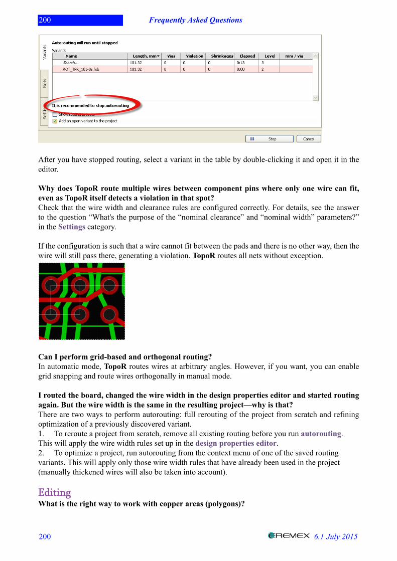
200 Frequently Asked Questions
200 6.1 July 2015
After you have stopped routing, select a variant in the table by double-clicking it and open it in theeditor.
Why does TopoR route multiple wires between component pins where only one wire can fit,even as TopoR itself detects a violation in that spot?Check that the wire width and clearance rules are configured correctly. For details, see the answerto the question “What's the purpose of the “nominal clearance” and “nominal width” parameters?”in the Settings category.
If the configuration is such that a wire cannot fit between the pads and there is no other way, then thewire will still pass there, generating a violation. TopoR routes all nets without exception.
Can I perform grid-based and orthogonal routing?In automatic mode, TopoR routes wires at arbitrary angles. However, if you want, you can enablegrid snapping and route wires orthogonally in manual mode.
I routed the board, changed the wire width in the design properties editor and started routingagain. But the wire width is the same in the resulting project—why is that?There are two ways to perform autorouting: full rerouting of the project from scratch and refiningoptimization of a previously discovered variant.1. To reroute a project from scratch, remove all existing routing before you run autorouting.This will apply the wire width rules set up in the design properties editor.2. To optimize a project, run autorouting from the context menu of one of the saved routingvariants. This will apply only those wire width rules that have already been used in the project(manually thickened wires will also be taken into account).
EditingWhat is the right way to work with copper areas (polygons)?
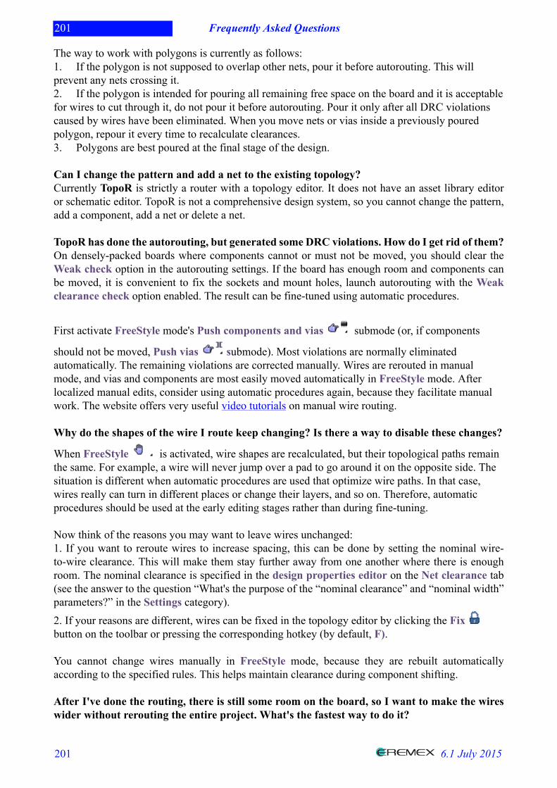
201 Frequently Asked Questions
201 6.1 July 2015
The way to work with polygons is currently as follows:1. If the polygon is not supposed to overlap other nets, pour it before autorouting. This willprevent any nets crossing it.2. If the polygon is intended for pouring all remaining free space on the board and it is acceptablefor wires to cut through it, do not pour it before autorouting. Pour it only after all DRC violationscaused by wires have been eliminated. When you move nets or vias inside a previously pouredpolygon, repour it every time to recalculate clearances.3. Polygons are best poured at the final stage of the design.
Can I change the pattern and add a net to the existing topology?Currently TopoR is strictly a router with a topology editor. It does not have an asset library editoror schematic editor. TopoR is not a comprehensive design system, so you cannot change the pattern,add a component, add a net or delete a net.
TopoR has done the autorouting, but generated some DRC violations. How do I get rid of them?On densely-packed boards where components cannot or must not be moved, you should clear theWeak check option in the autorouting settings. If the board has enough room and components canbe moved, it is convenient to fix the sockets and mount holes, launch autorouting with the Weakclearance check option enabled. The result can be fine-tuned using automatic procedures.
First activate FreeStyle mode's Push components and vias submode (or, if components
should not be moved, Push vias submode). Most violations are normally eliminatedautomatically. The remaining violations are corrected manually. Wires are rerouted in manualmode, and vias and components are most easily moved automatically in FreeStyle mode. Afterlocalized manual edits, consider using automatic procedures again, because they facilitate manualwork. The website offers very useful video tutorials on manual wire routing.
Why do the shapes of the wire I route keep changing? Is there a way to disable these changes?
When FreeStyle is activated, wire shapes are recalculated, but their topological paths remainthe same. For example, a wire will never jump over a pad to go around it on the opposite side. Thesituation is different when automatic procedures are used that optimize wire paths. In that case,wires really can turn in different places or change their layers, and so on. Therefore, automaticprocedures should be used at the early editing stages rather than during fine-tuning.
Now think of the reasons you may want to leave wires unchanged:1. If you want to reroute wires to increase spacing, this can be done by setting the nominal wire-to-wire clearance. This will make them stay further away from one another where there is enoughroom. The nominal clearance is specified in the design properties editor on the Net clearance tab(see the answer to the question “What's the purpose of the “nominal clearance” and “nominal width”parameters?” in the Settings category).2. If your reasons are different, wires can be fixed in the topology editor by clicking the Fix button on the toolbar or pressing the corresponding hotkey (by default, F).
You cannot change wires manually in FreeStyle mode, because they are rebuilt automaticallyaccording to the specified rules. This helps maintain clearance during component shifting.
After I've done the routing, there is still some room on the board, so I want to make the wireswider without rerouting the entire project. What's the fastest way to do it?
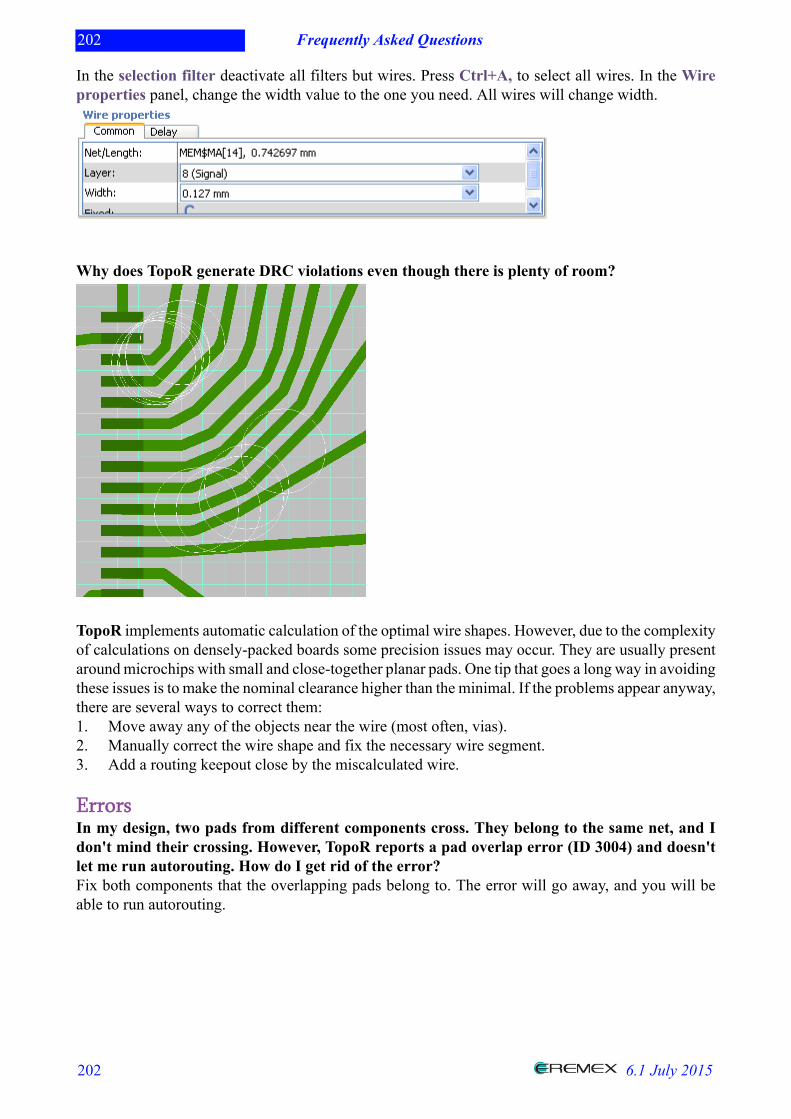
202 Frequently Asked Questions
202 6.1 July 2015
In the selection filter deactivate all filters but wires. Press Ctrl+A, to select all wires. In the Wireproperties panel, change the width value to the one you need. All wires will change width.
Why does TopoR generate DRC violations even though there is plenty of room?
TopoR implements automatic calculation of the optimal wire shapes. However, due to the complexityof calculations on densely-packed boards some precision issues may occur. They are usually presentaround microchips with small and close-together planar pads. One tip that goes a long way in avoidingthese issues is to make the nominal clearance higher than the minimal. If the problems appear anyway,there are several ways to correct them:1. Move away any of the objects near the wire (most often, vias).2. Manually correct the wire shape and fix the necessary wire segment.3. Add a routing keepout close by the miscalculated wire.
ErrorsIn my design, two pads from different components cross. They belong to the same net, and Idon't mind their crossing. However, TopoR reports a pad overlap error (ID 3004) and doesn'tlet me run autorouting. How do I get rid of the error?Fix both components that the overlapping pads belong to. The error will go away, and you will beable to run autorouting.
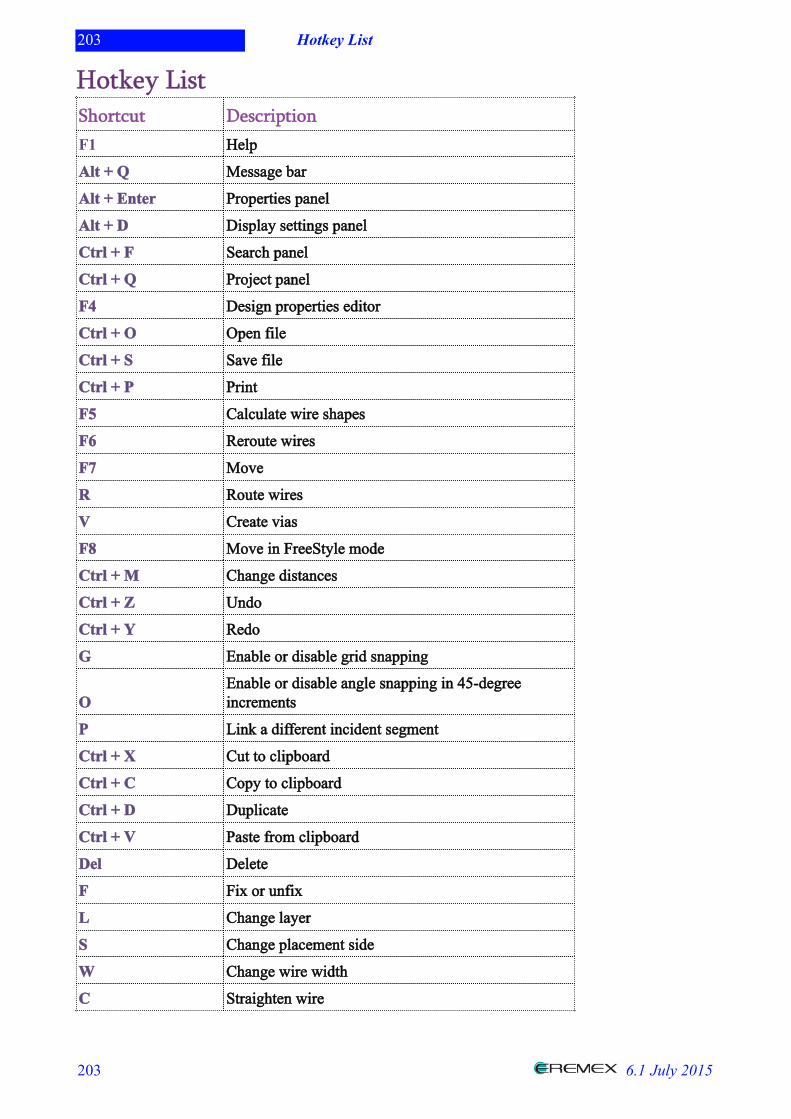
203 Hotkey List
203 6.1 July 2015
Hotkey ListShortcut DescriptionF1 Help
Alt + Q Message bar
Alt + Enter Properties panel
Alt + D Display settings panel
Ctrl + F Search panel
Ctrl + Q Project panel
F4 Design properties editor
Ctrl + O Open file
Ctrl + S Save file
Ctrl + P Print
F5 Calculate wire shapes
F6 Reroute wires
F7 Move
R Route wires
V Create vias
F8 Move in FreeStyle mode
Ctrl + M Change distances
Ctrl + Z Undo
Ctrl + Y Redo
G Enable or disable grid snapping
OEnable or disable angle snapping in 45-degreeincrements
P Link a different incident segment
Ctrl + X Cut to clipboard
Ctrl + C Copy to clipboard
Ctrl + D Duplicate
Ctrl + V Paste from clipboard
Del Delete
F Fix or unfix
L Change layer
S Change placement side
W Change wire width
C Straighten wire
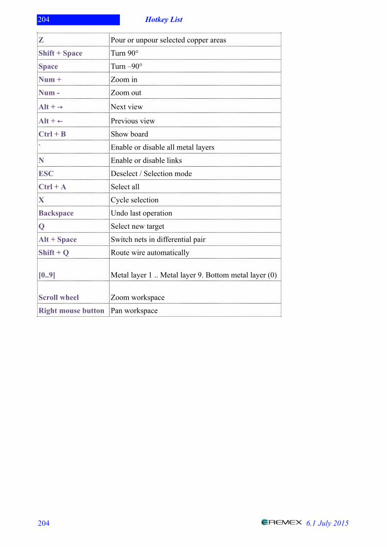
204 Hotkey List
204 6.1 July 2015
Z Pour or unpour selected copper areas
Shift + Space Turn 90°
Space Turn –90°
Num + Zoom in
Num - Zoom out
Alt + → Next view
Alt + ← Previous view
Ctrl + B Show board
` Enable or disable all metal layers
N Enable or disable links
ESC Deselect / Selection mode
Ctrl + A Select all
X Cycle selection
Backspace Undo last operation
Q Select new target
Alt + Space Switch nets in differential pair
Shift + Q Route wire automatically
[0..9] Metal layer 1 .. Metal layer 9. Bottom metal layer (0)
Scroll wheel Zoom workspace
Right mouse button Pan workspace
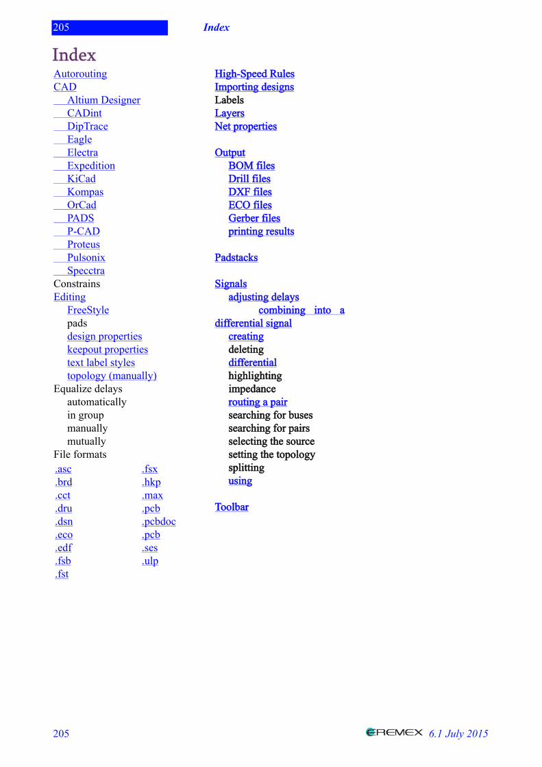
205 Index
205 6.1 July 2015
IndexAutoroutingCAD Altium Designer CADint DipTrace Eagle Electra Expedition KiCad Kompas OrCad PADS P-CAD Proteus Pulsonix SpecctraConstrainsEditing FreeStyle pads design properties keepout properties text label styles topology (manually)Equalize delays automatically in group manually mutuallyFile formats.asc.brd.cct.dru.dsn.eco.edf.fsb.fst
.fsx
.hkp
.max
.pcb
.pcbdoc
.pcb
.ses
.ulp
High-Speed RulesImporting designsLabelsLayersNet properties
Output BOM files Drill files DXF files ECO files Gerber files printing results
Padstacks
Signals adjusting delays combining into adifferential signal creating deleting differential highlighting impedance routing a pair searching for buses searching for pairs selecting the source setting the topology splitting using
Toolbar

206 About the TopoR PCB Format
206 6.1 July 2015
About the TopoR PCB FormatThe current version of the format is 1.1.2. The Topor PCB Format Specification for developers isavailable for download from the website: eda.eremex.com/downloads.
207 Working with single-layer borders
207 6.1 July 2015
Working with single-layer bordersTopoR offers specialized features that greatly facilitate routing of single-layer PCBs. Therecommended scenario for single-layer PCB routing is as follows: 1. After you have imported a project, check the routing rules carefully. The recommendednominal clearance to set is 1.5 times the minimal allowed clearance.2. Make sure that the board outline is set. It is better to define the outline as a single polygon thana series of lines.3. To prevent components running into one another during automatic placement, set thecomponent outlines. If component outlines are defined in custom layers, make sure you select theConsider during placement option for those layers in the Layers section.4. Perform component placement. Importantly, you should fix the components whose positionsare predefined; and conversely, unfix the components that you don't mind being moved.5. Autorouting ► Options
a. Enable the Single-layer routing option and select the layer to route.b. Enable the Weak clearance check option. This is needed because during single-layer routing
wires normally pass between components, and it is difficult to know in advance wherecomponents should be wide enough apart to make room for wires and how many wires shouldfit in there. If you leave the Weak clearance check option cleared, TopoR, will try to closelyfollow the existing clearance rules. For example, if you need to route four wires betweencomponents, but only three fit in, then the fourth wire will take a detour (which can interferewith the routing of other wires) or use a jumper. By enabling the Weak clearance check optionyou permit the router to move unfixed components apart slightly, so TopoR will be able to routeall four wires at the requisite location.
c. If arcs are acceptable, enable the Use arcs option.d. If necessary, enable the Reassign functionally equivalent component pads option.e. Do not enable the Reuse existing layout as a starting point option.
6. Launch autorouting and wait until the router stops turning out new variants frequently (itshould take about a minute). The program shows a hint when the time is right: Autorouting maybe stopped. Stop the procedure.7. Select a routing variant. For single-layer routing, the best variant is usually the one that has thefewest vias (the number of vias equals twice the number of jumpers), because when you go on toedit the layout, it will be easier to shorten a long wire by adding a jumper than to remove a jumper.8. Open the variant in the editor. Because weak clearance checking was used, there may beclearance violations. In the toolbar, right-click the triangle, select Move vias and components andreroute wires. This moves components further apart in dense areas and closer together in spaciousareas. It is recommended that you perform the operation multiple times.9. In the toolbar, right-click the triangle and select Move vias and reroute wires. The vias willbe placed in a more reasonable fashion. This is a useful operation to perform (by pressing F7) aftereach minor manual edit.10. Correct the nets that were routed poorly, move specific components to optimal locations and,if necessary, change the orientation of components. Before you transform a component, considerremoving the wires incident to it; this generates net lines, which can be helpful visually.11. Perform correct manual routing for those nets that must have a particular topology, andenable the Fix flexibly option for these nets. This option locks the net topology, including the vialocations, but does not lock the wire shapes. The autorouter recognizes this option and keeps thetopology of flexibly fixed nets unchanged; for example, it does not complete the routing of such anet if it has not been fully routed.
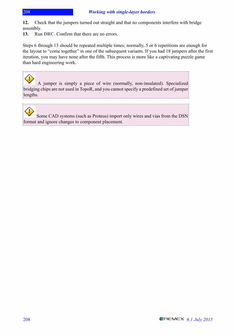
208 Working with single-layer borders
208 6.1 July 2015
12. Check that the jumpers turned out straight and that no components interfere with bridgeassembly.13. Run DRC. Confirm that there are no errors. Steps 6 through 13 should be repeated multiple times; normally, 5 or 6 repetitions are enough forthe layout to “come together” in one of the subsequent variants. If you had 18 jumpers after the firstiteration, you may have none after the fifth. This process is more like a captivating puzzle gamethan hard engineering work.
A jumper is simply a piece of wire (normally, non-insulated). Specializedbridging chips are not used in TopoR, and you cannot specify a predefined set of jumperlengths.
Some CAD systems (such as Proteus) import only wires and vias from the DSNformat and ignore changes to component placement.