mc33035 brushless dc motor controller - rs components
TRANSCRIPT
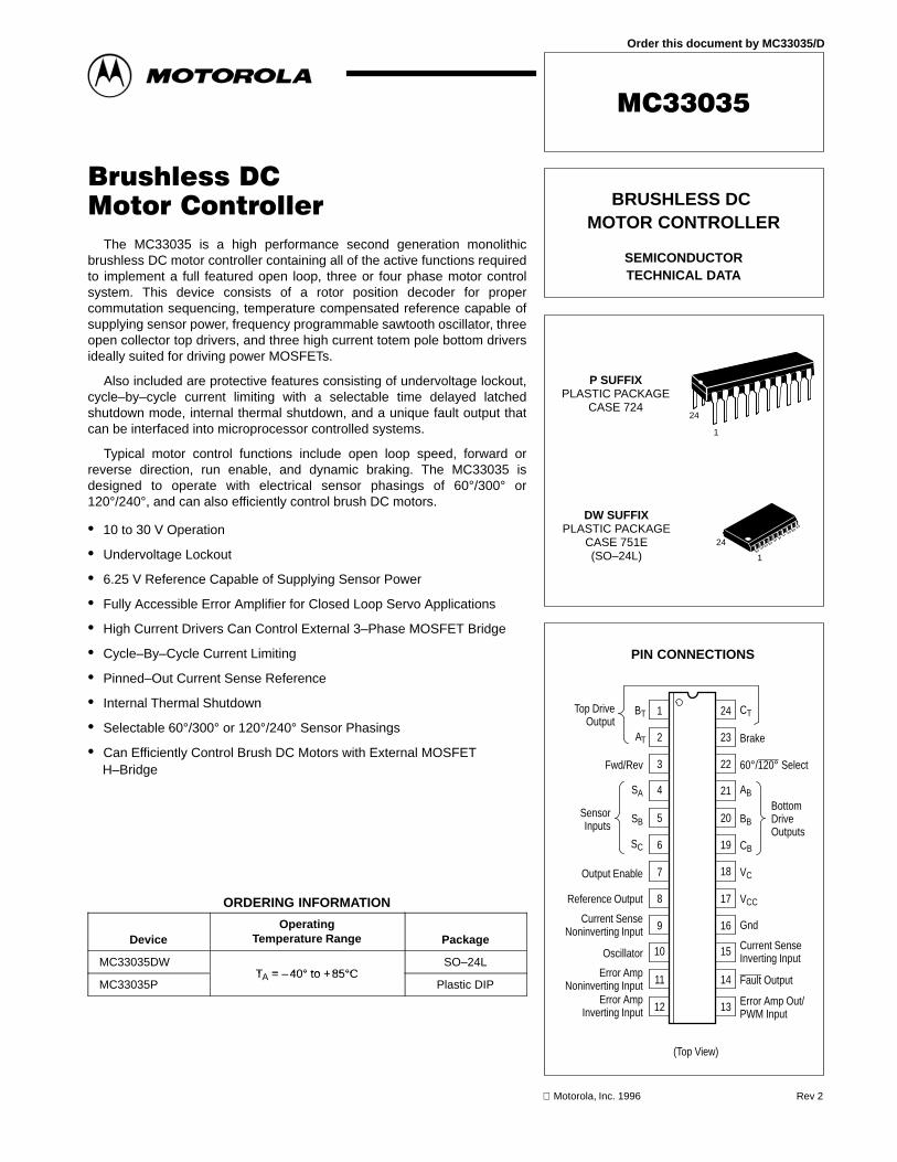
AT
BTTop DriveOutput
16
BottomDrive Outputs
15
(Top View)
17
18
19
20
21
10
9
8
7
6
5SensorInputs
4
Oscillator
Current SenseNoninverting Input
Reference Output
Output Enable
SC
SB
SA
60°/120° SelectFwd/Rev
Current SenseInverting Input
Gnd
VCC
CT
22
23
BB
CB
3
24
Brake2
AB
1
VC
SEMICONDUCTORTECHNICAL DATA
BRUSHLESS DC MOTOR CONTROLLER
PIN CONNECTIONS
Order this document by MC33035/D
24
1
24
1
P SUFFIXPLASTIC PACKAGE
CASE 724
DW SUFFIXPLASTIC PACKAGE
CASE 751E(SO–24L)
14
1312
11
Error AmpInverting Input
Error AmpNoninverting Input
Error Amp Out/PWM Input
Fault Output
1MOTOROLA ANALOG IC DEVICE DATA
The MC33035 is a high performance second generation monolithicbrushless DC motor controller containing all of the active functions requiredto implement a full featured open loop, three or four phase motor controlsystem. This device consists of a rotor position decoder for propercommutation sequencing, temperature compensated reference capable ofsupplying sensor power, frequency programmable sawtooth oscillator, threeopen collector top drivers, and three high current totem pole bottom driversideally suited for driving power MOSFETs.
Also included are protective features consisting of undervoltage lockout,cycle–by–cycle current limiting with a selectable time delayed latchedshutdown mode, internal thermal shutdown, and a unique fault output thatcan be interfaced into microprocessor controlled systems.
Typical motor control functions include open loop speed, forward orreverse direction, run enable, and dynamic braking. The MC33035 isdesigned to operate with electrical sensor phasings of 60°/300° or120°/240°, and can also efficiently control brush DC motors.
• 10 to 30 V Operation
• Undervoltage Lockout
• 6.25 V Reference Capable of Supplying Sensor Power
• Fully Accessible Error Amplifier for Closed Loop Servo Applications
• High Current Drivers Can Control External 3–Phase MOSFET Bridge
• Cycle–By–Cycle Current Limiting
• Pinned–Out Current Sense Reference
• Internal Thermal Shutdown
• Selectable 60°/300° or 120°/240° Sensor Phasings
• Can Efficiently Control Brush DC Motors with External MOSFETH–Bridge
ORDERING INFORMATION
DeviceOperating
Temperature Range Package
MC33035DWTA = –40° to +85°C
SO–24L
MC33035PTA = –40° to +85°C
Plastic DIP
Motorola, Inc. 1996 Rev 2
MC33035
2 MOTOROLA ANALOG IC DEVICE DATA
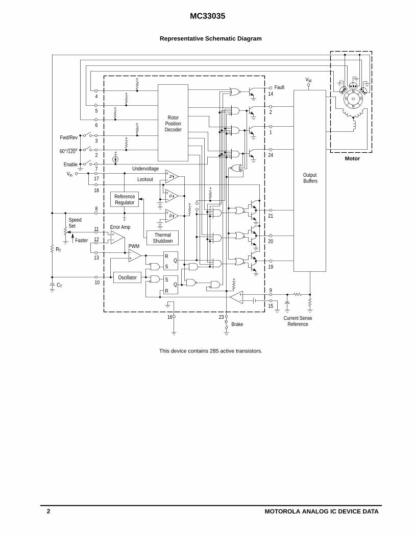
MotorEnable
QS
CT
RRT
Oscillator
Error Amp
PWM
ThermalShutdown
ReferenceRegulator
Lockout
UndervoltageVin
Fwd/Rev
QR
S
Faster
SS
VM
SpeedSet
This device contains 285 active transistors.
Representative Schematic Diagram
RotorPositionDecoder
Output Buffers
Current SenseReference
60°/120°
18
17
Brake
FaultN
N
7
2
3
6
5
4
8
11
12
13
10
14
2
1
24
21
20
19
9
15
2316
MC33035
3MOTOROLA ANALOG IC DEVICE DATA
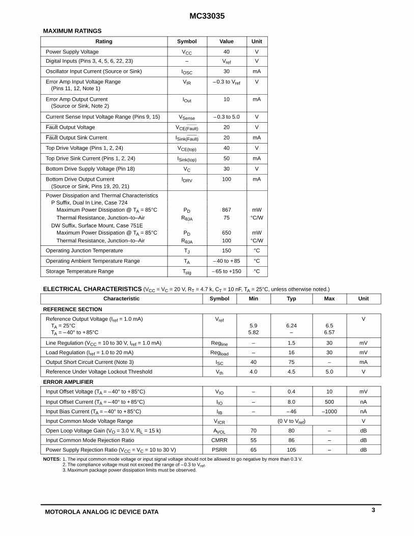
MAXIMUM RATINGS
Rating Symbol Value Unit
Power Supply Voltage VCC 40 V
Digital Inputs (Pins 3, 4, 5, 6, 22, 23) – Vref V
Oscillator Input Current (Source or Sink) IOSC 30 mA
Error Amp Input Voltage Range(Pins 11, 12, Note 1)
VIR –0.3 to Vref V
Error Amp Output Current(Source or Sink, Note 2)
IOut 10 mA
Current Sense Input Voltage Range (Pins 9, 15) VSense –0.3 to 5.0 V
Fault Output Voltage VCE(Fault) 20 V
Fault Output Sink Current ISink(Fault) 20 mA
Top Drive Voltage (Pins 1, 2, 24) VCE(top) 40 V
Top Drive Sink Current (Pins 1, 2, 24) ISink(top) 50 mA
Bottom Drive Supply Voltage (Pin 18) VC 30 V
Bottom Drive Output Current IDRV 100 mA(Source or Sink, Pins 19, 20, 21)
Power Dissipation and Thermal CharacteristicsP Suffix, Dual In Line, Case 724
Maximum Power Dissipation @ TA = 85°C PD 867 mW
Thermal Resistance, Junction–to–Air RθJA 75 °C/W
DW Suffix, Surface Mount, Case 751EMaximum Power Dissipation @ TA = 85°C PD 650 mW
Thermal Resistance, Junction–to–Air RθJA 100 °C/W
Operating Junction Temperature TJ 150 °C
Operating Ambient Temperature Range TA –40 to +85 °C
Storage Temperature Range Tstg –65 to +150 °C
ELECTRICAL CHARACTERISTICS (VCC = VC = 20 V, RT = 4.7 k, CT = 10 nF, TA = 25°C, unless otherwise noted.)
Characteristic Symbol Min Typ Max Unit
REFERENCE SECTION
Reference Output Voltage (Iref = 1.0 mA)TA = 25°CTA = –40° to +85°C
Vref5.95.82
6.24–
6.56.57
V
Line Regulation (VCC = 10 to 30 V, Iref = 1.0 mA) Regline – 1.5 30 mV
Load Regulation (Iref = 1.0 to 20 mA) Regload – 16 30 mV
Output Short Circuit Current (Note 3) ISC 40 75 – mA
Reference Under Voltage Lockout Threshold Vth 4.0 4.5 5.0 V
ERROR AMPLIFIER
Input Offset Voltage (TA = –40° to +85°C) VIO – 0.4 10 mV
Input Offset Current (TA = –40° to +85°C) IIO – 8.0 500 nA
Input Bias Current (TA = –40° to +85°C) IIB – –46 –1000 nA
Input Common Mode Voltage Range VICR (0 V to Vref) V
Open Loop Voltage Gain (VO = 3.0 V, RL = 15 k) AVOL 70 80 – dB
Input Common Mode Rejection Ratio CMRR 55 86 – dB
Power Supply Rejection Ratio (VCC = VC = 10 to 30 V) PSRR 65 105 – dB
NOTES: 1. The input common mode voltage or input signal voltage should not be allowed to go negative by more than 0.3 V.2. The compliance voltage must not exceed the range of – 0.3 to Vref.3. Maximum package power dissipation limits must be observed.

MC33035
4 MOTOROLA ANALOG IC DEVICE DATA
ELECTRICAL CHARACTERISTICS (continued) (VCC = VC = 20 V, RT = 4.7 k, CT = 10 nF, TA = 25°C, unless otherwise noted.)
Characteristic Symbol Min Typ Max Unit
ERROR AMPLIFIER
Output Voltage SwingHigh State (RL = 15 k to Gnd)Low State (RL = 15 k to Vref)
VOHVOL
4.6–
5.30.5
–1.0
V
OSCILLATOR SECTION
Oscillator Frequency fOSC 22 25 28 kHz
Frequency Change with Voltage (VCC = 10 to 30 V) ∆fOSC/∆V – 0.01 5.0 %
Sawtooth Peak Voltage VOSC(P) – 4.1 4.5 V
Sawtooth Valley Voltage VOSC(V) 1.2 1.5 – V
LOGIC INPUTS
Input Threshold Voltage (Pins 3, 4, 5, 6, 7, 22, 23)High StateLow State
VIHVIL
3.0–
2.21.7
–0.8
V
Sensor Inputs (Pins 4, 5, 6)High State Input Current (VIH = 5.0 V)Low State Input Current (VIL = 0 V)
IIHIIL
–150–600
–70–337
–20–150
µA
Forward/Reverse, 60°/120° Select (Pins 3, 22, 23)High State Input Current (VIH = 5.0 V)Low State Input Current (VIL = 0 V)
IIHIIL
–75–300
–36–175
–10–75
µA
Output Enable µAOutput EnableHigh State Input Current (VIH = 5.0 V)L S I C (V 0 V)
IIHI
–6060
–2929
–1010
µAg p ( IH )
Low State Input Current (VIL = 0 V)IHIIL –60 –29 –10
CURRENT–LIMIT COMPARATOR
Threshold Voltage Vth 85 101 115 mV
Input Common Mode Voltage Range VICR – 3.0 – V
Input Bias Current IIB – –0.9 –5.0 µA
OUTPUTS AND POWER SECTIONS
Top Drive Output Sink Saturation (Isink = 25 mA) VCE(sat) – 0.5 1.5 V
Top Drive Output Off–State Leakage (VCE = 30 V) IDRV(leak) – 0.06 100 µA
Top Drive Output Switching Time (CL = 47 pF, RL = 1.0 k) ns
Rise Time tr – 107 300Fall Time tf – 26 300
Bottom Drive Output Voltage VBottom Drive Output VoltageHigh State (VCC = 20 V, VC = 30 V, Isource = 50 mA)L S (V 20 V V 30 V I 0 A)
VOHV
(VCC –2.0) (VCC –1.1)1
–2 0
Vg ( CC C source )
Low State (VCC = 20 V, VC = 30 V, Isink = 50 mA)OH
VOL
( CC )–
( CC )1.5 2.0
Bottom Drive Output Switching Time (CL = 1000 pF) ns
Rise Time tr – 38 200Fall Time tf – 30 200
Fault Output Sink Saturation (Isink = 16 mA) VCE(sat) – 225 500 mV
Fault Output Off–State Leakage (VCE = 20 V) IFLT(leak) – 1.0 100 µA
Under Voltage Lockout V
Drive Output Enabled (VCC or VC Increasing) Vth(on) 8.2 8.9 10Hysteresis VH 0.1 0.2 0.3
Power Supply Current mAPower Supply CurrentPin 17 (VCC = VC = 20 V) ICC – 12 16
mAPin 17 (VCC VC 20 V)Pin 17 (VCC = 20 V, VC = 30 V)
ICC–
1214
1620( CC 0 , C 30 )
Pin 18 (VCC = VC = 20 V) IC – 3.50
6.0( CC C )Pin 18 (VCC = 20 V, VC = 30 V)
C– 5.0 10
MC33035
5MOTOROLA ANALOG IC DEVICE DATA
V sat
, OU
TPU
T SA
TUR
ATIO
N V
OLT
AGE
(V)
5.0 µs/DIV
AV = +1.0No LoadTA = 25°C
, OU
TPU
T VO
LTAG
E (V
)O
4.5
3.0
1.5
1.0 µs/DIV
AV = +1.0No LoadTA = 25°C
3.05
3.0
2.95
Gnd
Vref
IO, OUTPUT LOAD CURRENT (mA)f, FREQUENCY (Hz)
56
1.0 k
220
200
180
160
140
120
100
80
60
– 24–16
– 8.0
0
8.0
16
24
32
40
48
10 M1.0 M100 k10 k
40
240
AVO
L, OPE
N L
OO
P VO
LTAG
E G
AIN
(dB)
EXC
ESS
PHAS
E (D
EGR
EES)
,φ
Phase
Gain
TA, AMBIENT TEMPERATURE (°C)
– 55– 4.0
– 2.0
0
2.0
125
4.0
1007550250– 25
f OSC
OSC
ILLA
TOR
FR
EQU
ENC
Y C
HAN
GE
(%)
,∆
100
CT = 1.0 nFCT = 100 nF
1.0
RT, TIMING RESISTOR (kΩ)
1000100100
10
f OSC
OSC
ILLA
TOR
FR
EQU
ENC
Y (k
Hz)
, CT = 10 nF
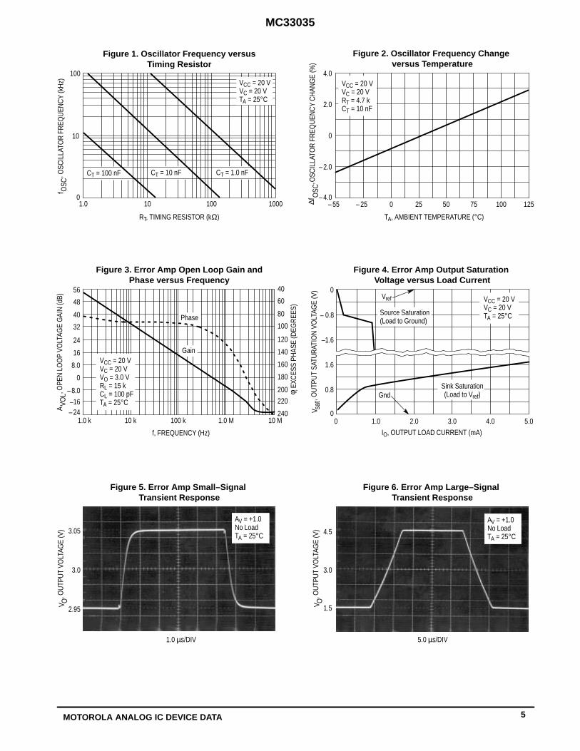
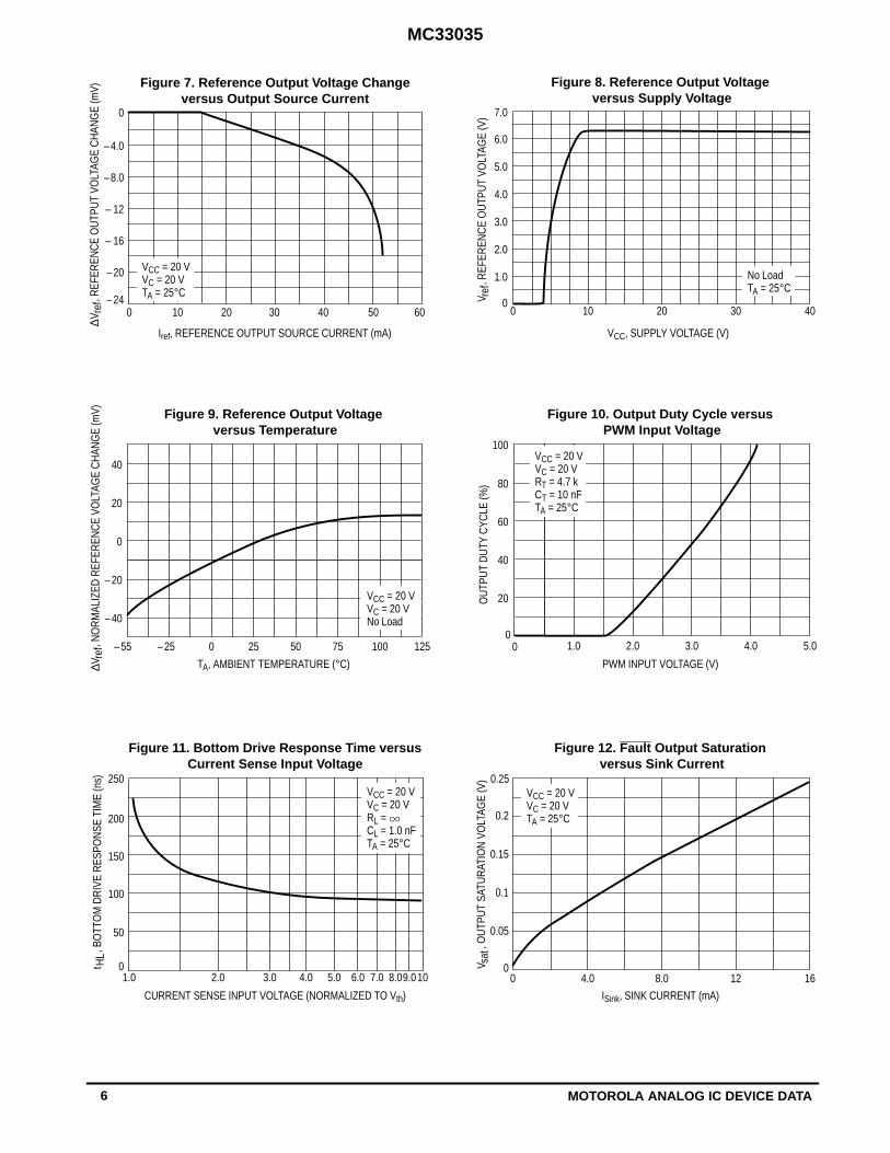
Figure 1. Oscillator Frequency versusTiming Resistor
Figure 2. Oscillator Frequency Change versus Temperature
Figure 3. Error Amp Open Loop Gain andPhase versus Frequency
Figure 4. Error Amp Output Saturation Voltage versus Load Current
Figure 5. Error Amp Small–Signal Transient Response
Figure 6. Error Amp Large–Signal Transient Response
0
1.0 2.00
– 0.8
–1.6
1.6
0.8
5.04.03.00
VCC = 20 VVC = 20 VTA = 25°C
VCC = 20 VVC = 20 VRT = 4.7 kCT = 10 nF
Source Saturation(Load to Ground)
VCC = 20 VVC = 20 VTA = 25°C
Sink Saturation(Load to Vref)
V
, OU
TPU
T VO
LTAG
E (V
)OV
VCC = 20 VVC = 20 VVO = 3.0 VRL = 15 kCL = 100 pFTA = 25°C
MC33035
6 MOTOROLA ANALOG IC DEVICE DATA
, OU
TPU
T SA
TUR
ATIO
N V
OLT
AGE
(V)
V sat
0
ISink, SINK CURRENT (mA)
0 16128.04.0
0.25
0.2
0.05
0
TA, AMBIENT TEMPERATURE (°C)
– 25
– 40
– 20
– 55 0
40
20
125100755025, NO
RM
ALIZ
ED R
EFER
ENC
E VO
LTAG
E C
HAN
GE
(mV)
∆Vre
f
0
Iref, REFERENCE OUTPUT SOURCE CURRENT (mA)
0
605040302010– 24
– 20
– 4.0
– 8.0
– 12
– 16
V ref
, REF
EREN
CE
OU
TPU
T VO
LTAG
E C
HAN
GE
(mV)
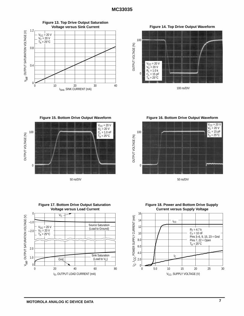
∆Figure 7. Reference Output Voltage Change
versus Output Source CurrentFigure 8. Reference Output Voltage
versus Supply Voltage
Figure 9. Reference Output Voltage versus Temperature
Figure 10. Output Duty Cycle versus PWM Input Voltage
Figure 11. Bottom Drive Response Time versusCurrent Sense Input Voltage
Figure 12. Fault Output Saturation versus Sink Current
00
7.0
00
VCC, SUPPLY VOLTAGE (V)
6.0
40302010
5.0
4.0
3.0
2.0
1.0
V ref
, REF
EREN
CE
OU
TPU
T VO
LTAG
E (V
)
5.04.03.02.01.0
100
80
60
40
20
PWM INPUT VOLTAGE (V)
OU
TPU
T D
UTY
CYC
LE (%
)
0
CURRENT SENSE INPUT VOLTAGE (NORMALIZED TO Vth)
50
100
150
200
250
1.0 2.0 3.0 4.0 5.0 7.0 8.0 10
t HL,
BO
TTO
M D
RIV
E R
ESPO
NSE
TIM
E (n
s)
No LoadTA = 25°C
VCC = 20 VVC = 20 VNo Load
6.0 9.0
VCC = 20 VVC = 20 VTA = 25°C
VCC = 20 VVC = 20 VRT = 4.7 kCT = 10 nFTA = 25°C
VCC = 20 VVC = 20 VRL = CL = 1.0 nFTA = 25°C
0.15
0.1
VCC = 20 VVC = 20 VTA = 25°C
MC33035
7MOTOROLA ANALOG IC DEVICE DATA
1.0
OU
TPU
T VO
LTAG
E (%
)
Gnd
VC
– 2.0
40
0
IO, OUTPUT LOAD CURRENT (mA)
00
–1.0
2.0
806020
, OU
TPU
T SA
TUR
ATIO
N V
OLT
AGE
(V)
sat
Sink Saturation(Load to VC)
Source Saturation(Load to Ground)VCC = 20 V
VC = 20 VTA = 25°C
V
VCC = 20 VVC = 20 VTA = 25°C
50 ns/DIV
VCC = 20 VVC = 20 VCL = 1.0 nFTA = 25°C
100 ns/DIV
VCC = 20 VVC = 20 VRL = 1.0 kCL = 15 pFTA = 25°C
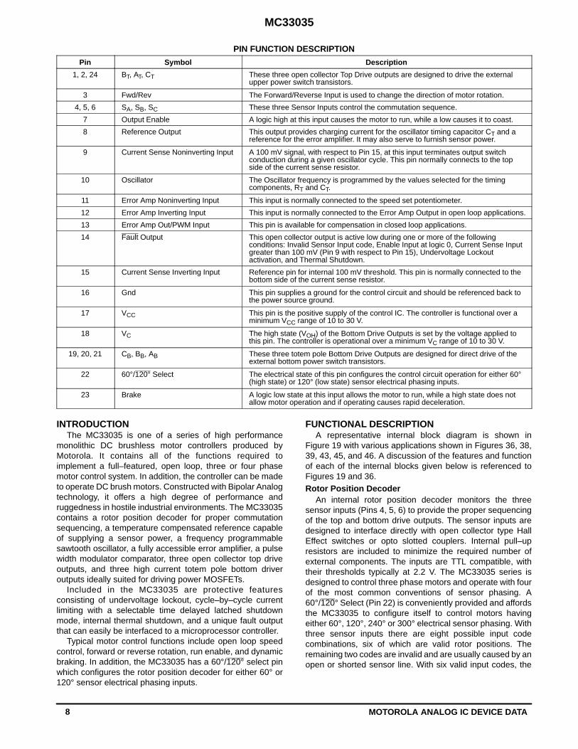
Figure 13. Top Drive Output SaturationVoltage versus Sink Current Figure 14. Top Drive Output Waveform
Figure 15. Bottom Drive Output Waveform Figure 16. Bottom Drive Output Waveform
200
0ISink, SINK CURRENT (mA)
10 30 40
0.4
0.8
1.2
V sat
, OU
TPU
T SA
TUR
ATIO
N V
OLT
AGE
(V)
Figure 17. Bottom Drive Output Saturation Voltage versus Load Current
50 ns/DIV
VCC = 20 VVC = 20 VCL = 15 pFTA = 25°C
Figure 18. Power and Bottom Drive Supply Current versus Supply Voltage
16
14
12
10
8.0
6.0
4.0
2.0
0
, PO
WER
SU
PPLY
CU
RR
ENT
(mA)
CC
, I
0 5.0 10 15 20 25 30
CI
RT = 4.7 kCT = 10 nFPins 3–6, 9, 15, 23 = GndPins 7, 22 = OpenTA = 25°C
VCC, SUPPLY VOLTAGE (V)
ICC
IC
100
0
100
0
100
0
OU
TPU
T VO
LTAG
E (%
)O
UTP
UT
VOLT
AGE
(%)
MC33035
8 MOTOROLA ANALOG IC DEVICE DATA
PIN FUNCTION DESCRIPTION
Pin Symbol Description
1, 2, 24 BT, AT, CT These three open collector Top Drive outputs are designed to drive the externalupper power switch transistors.
3 Fwd/Rev The Forward/Reverse Input is used to change the direction of motor rotation.
4, 5, 6 SA, SB, SC These three Sensor Inputs control the commutation sequence.
7 Output Enable A logic high at this input causes the motor to run, while a low causes it to coast.
8 Reference Output This output provides charging current for the oscillator timing capacitor CT and areference for the error amplifier. It may also serve to furnish sensor power.
9 Current Sense Noninverting Input A 100 mV signal, with respect to Pin 15, at this input terminates output switchconduction during a given oscillator cycle. This pin normally connects to the topside of the current sense resistor.
10 Oscillator The Oscillator frequency is programmed by the values selected for the timingcomponents, RT and CT.
11 Error Amp Noninverting Input This input is normally connected to the speed set potentiometer.
12 Error Amp Inverting Input This input is normally connected to the Error Amp Output in open loop applications.
13 Error Amp Out/PWM Input This pin is available for compensation in closed loop applications.
14 Fault Output This open collector output is active low during one or more of the followingconditions: Invalid Sensor Input code, Enable Input at logic 0, Current Sense Inputgreater than 100 mV (Pin 9 with respect to Pin 15), Undervoltage Lockoutactivation, and Thermal Shutdown.
15 Current Sense Inverting Input Reference pin for internal 100 mV threshold. This pin is normally connected to thebottom side of the current sense resistor.
16 Gnd This pin supplies a ground for the control circuit and should be referenced back tothe power source ground.
17 VCC This pin is the positive supply of the control IC. The controller is functional over aminimum VCC range of 10 to 30 V.
18 VC The high state (VOH) of the Bottom Drive Outputs is set by the voltage applied tothis pin. The controller is operational over a minimum VC range of 10 to 30 V.
19, 20, 21 CB, BB, AB These three totem pole Bottom Drive Outputs are designed for direct drive of theexternal bottom power switch transistors.
22 60°/120° Select The electrical state of this pin configures the control circuit operation for either 60°(high state) or 120° (low state) sensor electrical phasing inputs.
23 Brake A logic low state at this input allows the motor to run, while a high state does notallow motor operation and if operating causes rapid deceleration.
INTRODUCTIONThe MC33035 is one of a series of high performance
monolithic DC brushless motor controllers produced byMotorola. It contains all of the functions required toimplement a full–featured, open loop, three or four phasemotor control system. In addition, the controller can be madeto operate DC brush motors. Constructed with Bipolar Analogtechnology, it offers a high degree of performance andruggedness in hostile industrial environments. The MC33035contains a rotor position decoder for proper commutationsequencing, a temperature compensated reference capableof supplying a sensor power, a frequency programmablesawtooth oscillator, a fully accessible error amplifier, a pulsewidth modulator comparator, three open collector top driveoutputs, and three high current totem pole bottom driveroutputs ideally suited for driving power MOSFETs.
Included in the MC33035 are protective featuresconsisting of undervoltage lockout, cycle–by–cycle currentlimiting with a selectable time delayed latched shutdownmode, internal thermal shutdown, and a unique fault outputthat can easily be interfaced to a microprocessor controller.
Typical motor control functions include open loop speedcontrol, forward or reverse rotation, run enable, and dynamicbraking. In addition, the MC33035 has a 60°/120° select pinwhich configures the rotor position decoder for either 60° or120° sensor electrical phasing inputs.
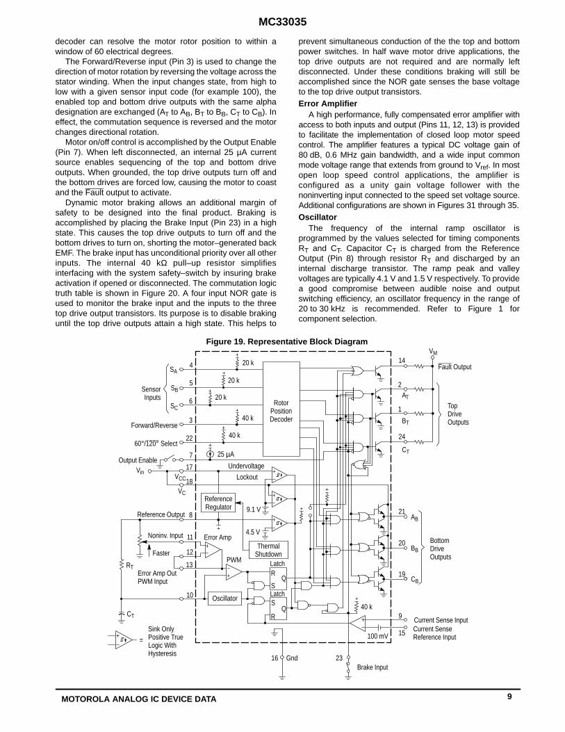
FUNCTIONAL DESCRIPTIONA representative internal block diagram is shown in
Figure 19 with various applications shown in Figures 36, 38,39, 43, 45, and 46. A discussion of the features and functionof each of the internal blocks given below is referenced toFigures 19 and 36.Rotor Position Decoder
An internal rotor position decoder monitors the threesensor inputs (Pins 4, 5, 6) to provide the proper sequencingof the top and bottom drive outputs. The sensor inputs aredesigned to interface directly with open collector type HallEffect switches or opto slotted couplers. Internal pull–upresistors are included to minimize the required number ofexternal components. The inputs are TTL compatible, withtheir thresholds typically at 2.2 V. The MC33035 series isdesigned to control three phase motors and operate with fourof the most common conventions of sensor phasing. A60°/120° Select (Pin 22) is conveniently provided and affordsthe MC33035 to configure itself to control motors havingeither 60°, 120°, 240° or 300° electrical sensor phasing. Withthree sensor inputs there are eight possible input codecombinations, six of which are valid rotor positions. Theremaining two codes are invalid and are usually caused by anopen or shorted sensor line. With six valid input codes, the
MC33035
9MOTOROLA ANALOG IC DEVICE DATA
decoder can resolve the motor rotor position to within awindow of 60 electrical degrees.
The Forward/Reverse input (Pin 3) is used to change thedirection of motor rotation by reversing the voltage across thestator winding. When the input changes state, from high tolow with a given sensor input code (for example 100), theenabled top and bottom drive outputs with the same alphadesignation are exchanged (AT to AB, BT to BB, CT to CB). Ineffect, the commutation sequence is reversed and the motorchanges directional rotation.
Motor on/off control is accomplished by the Output Enable(Pin 7). When left disconnected, an internal 25 µA currentsource enables sequencing of the top and bottom driveoutputs. When grounded, the top drive outputs turn off andthe bottom drives are forced low, causing the motor to coastand the Fault output to activate.
Dynamic motor braking allows an additional margin ofsafety to be designed into the final product. Braking isaccomplished by placing the Brake Input (Pin 23) in a highstate. This causes the top drive outputs to turn off and thebottom drives to turn on, shorting the motor–generated backEMF. The brake input has unconditional priority over all otherinputs. The internal 40 kΩ pull–up resistor simplifiesinterfacing with the system safety–switch by insuring brakeactivation if opened or disconnected. The commutation logictruth table is shown in Figure 20. A four input NOR gate isused to monitor the brake input and the inputs to the threetop drive output transistors. Its purpose is to disable brakinguntil the top drive outputs attain a high state. This helps to
prevent simultaneous conduction of the the top and bottompower switches. In half wave motor drive applications, thetop drive outputs are not required and are normally leftdisconnected. Under these conditions braking will still beaccomplished since the NOR gate senses the base voltageto the top drive output transistors.Error Amplifier
A high performance, fully compensated error amplifier withaccess to both inputs and output (Pins 11, 12, 13) is providedto facilitate the implementation of closed loop motor speedcontrol. The amplifier features a typical DC voltage gain of80 dB, 0.6 MHz gain bandwidth, and a wide input commonmode voltage range that extends from ground to Vref. In mostopen loop speed control applications, the amplifier isconfigured as a unity gain voltage follower with thenoninverting input connected to the speed set voltage source.Additional configurations are shown in Figures 31 through 35.Oscillator
The frequency of the internal ramp oscillator isprogrammed by the values selected for timing componentsRT and CT. Capacitor CT is charged from the ReferenceOutput (Pin 8) through resistor RT and discharged by aninternal discharge transistor. The ramp peak and valleyvoltages are typically 4.1 V and 1.5 V respectively. To providea good compromise between audible noise and outputswitching efficiency, an oscillator frequency in the range of20 to 30 kHz is recommended. Refer to Figure 1 forcomponent selection.
15
24
20
2
1
21
19
VM
TopDriveOutputs
BottomDriveOutputs
CB
Current Sense Reference Input
BB
AB
AT
BT
CT
QS
R
Oscillator
Error Amp
PWM
ThermalShutdown
ReferenceRegulator
Lockout
Undervoltage
QR
S
RotorPositionDecoder
Brake Input
Figure 19. Representative Block Diagram
60°/120° Select
Output Enable
CT
RT
Vin
4
10
11
13
8
12
3
17
22
7
6
5
Forward/Reverse
Faster
Noninv. Input
SA
SC
SBSensorInputs
Error Amp OutPWM Input
Sink OnlyPositive TrueLogic WithHysteresis
=
Reference Output
16
Latch
Latch
23Gnd
14
9 Current Sense Input
Fault Output20 k
20 k
20 k
40 k
40 k
25 µA
VCC
VC
18
9.1 V
4.5 V
100 mV
40 k
MC33035
10 MOTOROLA ANALOG IC DEVICE DATA
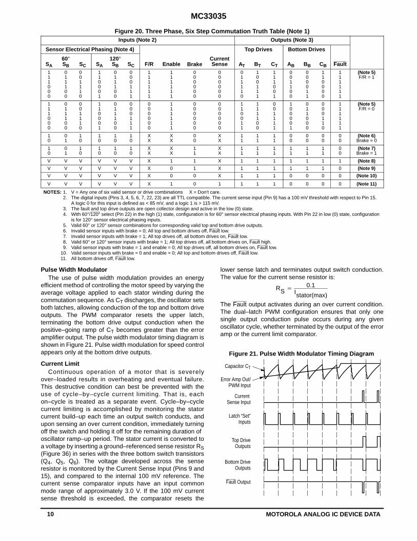
Figure 20. Three Phase, Six Step Commutation Truth Table (Note 1)Inputs (Note 2) Outputs (Note 3)
Sensor Electrical Phasing (Note 4) Top Drives Bottom Drives
SA
60°SB SC SA
120°SB SC F/R Enable Brake
CurrentSense AT BT CT AB BB CB Fault
111000
011100
001110
110001
011100
000111
111111
111111
000000
000000
011110
100111
111001
001100
000011
110000
111111
(Note 5)F/R = 1
111000
011100
001110
110001
011100
000111
000000
111111
000000
000000
110011
111100
001111
100001
011000
000110
111111
(Note 5)F/R = 0
10
01
10
10
10
10
XX
XX
00
XX
11
11
11
00
00
00
00
(Note 6)Brake = 0
10
01
10
10
10
10
XX
XX
11
XX
11
11
11
11
11
11
00
(Note 7)Brake = 1
V V V V V V X 1 1 X 1 1 1 1 1 1 1 (Note 8)
V V V V V V X 0 1 X 1 1 1 1 1 1 0 (Note 9)
V V V V V V X 0 0 X 1 1 1 0 0 0 0 (Note 10)
V V V V V V X 1 0 1 1 1 1 0 0 0 0 (Note 11)
NOTES: 1. V = Any one of six valid sensor or drive combinations X = Don’t care.2. The digital inputs (Pins 3, 4, 5, 6, 7, 22, 23) are all TTL compatible. The current sense input (Pin 9) has a 100 mV threshold with respect to Pin 15.
A logic 0 for this input is defined as < 85 mV, and a logic 1 is > 115 mV.3. The fault and top drive outputs are open collector design and active in the low (0) state.4. With 60°/120° select (Pin 22) in the high (1) state, configuration is for 60° sensor electrical phasing inputs. With Pin 22 in low (0) state, configuration
is for 120° sensor electrical phasing inputs.5. Valid 60° or 120° sensor combinations for corresponding valid top and bottom drive outputs.6. Invalid sensor inputs with brake = 0; All top and bottom drives off, Fault low.7. Invalid sensor inputs with brake = 1; All top drives off, all bottom drives on, Fault low.8. Valid 60° or 120° sensor inputs with brake = 1; All top drives off, all bottom drives on, Fault high.9. Valid sensor inputs with brake = 1 and enable = 0; All top drives off, all bottom drives on, Fault low.
10. Valid sensor inputs with brake = 0 and enable = 0; All top and bottom drives off, Fault low.11. All bottom drives off, Fault low.
Pulse Width ModulatorThe use of pulse width modulation provides an energy
efficient method of controlling the motor speed by varying theaverage voltage applied to each stator winding during thecommutation sequence. As CT discharges, the oscillator setsboth latches, allowing conduction of the top and bottom driveoutputs. The PWM comparator resets the upper latch,terminating the bottom drive output conduction when thepositive–going ramp of CT becomes greater than the erroramplifier output. The pulse width modulator timing diagram isshown in Figure 21. Pulse width modulation for speed controlappears only at the bottom drive outputs.
Current LimitContinuous operation of a motor that is severely
over–loaded results in overheating and eventual failure.This destructive condition can best be prevented with theuse of cycle–by–cycle current limiting. That is, eachon–cycle is treated as a separate event. Cycle–by–cyclecurrent limiting is accomplished by monitoring the statorcurrent build–up each time an output switch conducts, andupon sensing an over current condition, immediately turningoff the switch and holding it off for the remaining duration ofoscillator ramp–up period. The stator current is converted toa voltage by inserting a ground–referenced sense resistor RS(Figure 36) in series with the three bottom switch transistors(Q4, Q5, Q6). The voltage developed across the senseresistor is monitored by the Current Sense Input (Pins 9 and15), and compared to the internal 100 mV reference. Thecurrent sense comparator inputs have an input commonmode range of approximately 3.0 V. If the 100 mV currentsense threshold is exceeded, the comparator resets the
lower sense latch and terminates output switch conduction.The value for the current sense resistor is:
RS0.1
Istator(max)
The Fault output activates during an over current condition.The dual–latch PWM configuration ensures that only onesingle output conduction pulse occurs during any givenoscillator cycle, whether terminated by the output of the erroramp or the current limit comparator.
Figure 21. Pulse Width Modulator Timing Diagram
Current Sense Input
Capacitor CT
Error Amp Out/PWM Input
Latch “Set”Inputs
Top DriveOutputs
Bottom DriveOutputs
Fault Output
MC33035
11MOTOROLA ANALOG IC DEVICE DATA
ReferenceThe on–chip 6.25 V regulator (Pin 8) provides charging
current for the oscillator timing capacitor, a reference for theerror amplifier, and can supply 20 mA of current suitable fordirectly powering sensors in low voltage applications. Inhigher voltage applications, it may become necessary totransfer the power dissipated by the regulator off the IC. Thisis easily accomplished with the addition of an external passtransistor as shown in Figure 22. A 6.25 V reference levelwas chosen to allow implementation of the simpler NPNcircuit, where Vref – VBE exceeds the minimum voltagerequired by Hall Effect sensors over temperature. Withproper transistor selection and adequate heatsinking, up toone amp of load current can be obtained.
Figure 22. Reference Output Buffers
The NPN circuit is recommended for powering Hall or opto sensors, where theoutput voltage temperature coefficient is not critical. The PNP circuit is slightlymore complex, but is also more accurate over temperature. Neither circuit hascurrent limiting.
ToControlCircuitry6.25 V
SensorPower≈ 5.6 V
MPSU51A
Vin
MPSU01A
Vin
To Control Circuitryand Sensor Power
6.25 V
UVLO1739
REF
80.1
REF
8
18
UVLO17
18
Undervoltage LockoutA triple Undervoltage Lockout has been incorporated to
prevent damage to the IC and the external power switchtransistors. Under low power supply conditions, it guaranteesthat the IC and sensors are fully functional, and that there issufficient bottom drive output voltage. The positive powersupplies to the IC (VCC) and the bottom drives (VC) are eachmonitored by separate comparators that have theirthresholds at 9.1 V. This level ensures sufficient gate drivenecessary to attain low RDS(on) when driving standard powerMOSFET devices. When directly powering the Hall sensorsfrom the reference, improper sensor operation can result ifthe reference output voltage falls below 4.5 V. A thirdcomparator is used to detect this condition. If one or more ofthe comparators detects an undervoltage condition, the FaultOutput is activated, the top drives are turned off and thebottom drive outputs are held in a low state. Each of the
comparators contain hysteresis to prevent oscillations whencrossing their respective thresholds.
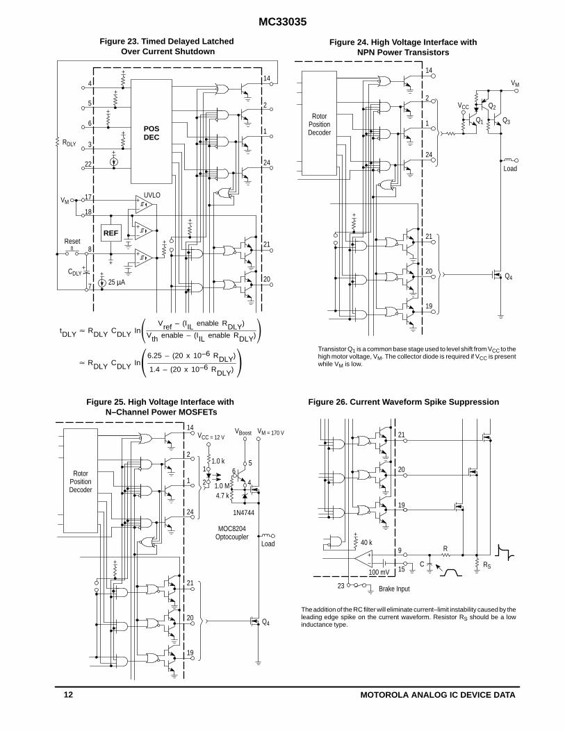
Fault OutputThe open collector Fault Output (Pin 14) was designed to
provide diagnostic information in the event of a systemmalfunction. It has a sink current capability of 16 mA andcan directly drive a light emitting diode for visual indication.Additionally, it is easily interfaced with TTL/CMOS logic foruse in a microprocessor controlled system. The FaultOutput is active low when one or more of the followingconditions occur:
1) Invalid Sensor Input code2) Output Enable at logic [0]3) Current Sense Input greater than 100 mV4) Undervoltage Lockout, activation of one or more of
the comparators5) Thermal Shutdown, maximum junction temperature
being exceededThis unique output can also be used to distinguish
between motor start–up or sustained operation in anoverloaded condition. With the addition of an RC networkbetween the Fault Output and the enable input, it is possibleto create a time–delayed latched shutdown for overcurrent.The added circuitry shown in Figure 23 makes easy startingof motor systems which have high inertial loads by providingadditional starting torque, while still preserving overcurrentprotection. This task is accomplished by setting the currentlimit to a higher than nominal value for a predetermined time.During an excessively long overcurrent condition, capacitorCDLY will charge, causing the enable input to cross itsthreshold to a low state. A latch is then formed by the positivefeedback loop from the Fault Output to the Output Enable.Once set, by the Current Sense Input, it can only be reset byshorting CDLY or cycling the power supplies.
Drive OutputsThe three top drive outputs (Pins 1, 2, 24) are open
collector NPN transistors capable of sinking 50 mA with aminimum breakdown of 30 V. Interfacing into higher voltageapplications is easily accomplished with the circuits shown inFigures 24 and 25.
The three totem pole bottom drive outputs (Pins 19, 20,21) are particularly suited for direct drive of N–ChannelMOSFETs or NPN bipolar transistors (Figures 26, 27, 28and 29). Each output is capable of sourcing and sinking upto 100 mA. Power for the bottom drives is supplied from VC(Pin 18). This separate supply input allows the designeradded flexibility in tailoring the drive voltage, independent ofVCC. A zener clamp should be connected to this input whendriving power MOSFETs in systems where VCC is greaterthan 20 V so as to prevent rupture of the MOSFET gates.
The control circuitry ground (Pin 16) and current senseinverting input (Pin 15) must return on separate paths to thecentral input source ground.
Thermal ShutdownInternal thermal shutdown circuitry is provided to protect
the IC in the event the maximum junction temperature isexceeded. When activated, typically at 170°C, the IC actsas though the Output Enable was grounded.
MC33035
12 MOTOROLA ANALOG IC DEVICE DATA
tDLY RDLY CDLY In Vref – (IIL enable RDLY)
Vth enable – (IIL enable RDLY)
Figure 23. Timed Delayed Latched Over Current Shutdown
24
20
2
1
21
REF
UVLO
Reset
POSDEC
4
8
3
17
22
7
6
5
14
VM
CDLY
25 µA
Load
Figure 24. High Voltage Interface withNPN Power Transistors
Transistor Q1 is a common base stage used to level shift from VCC to thehigh motor voltage, VM. The collector diode is required if VCC is presentwhile VM is low.
Q2
RDLY CDLY In6.25 – (20 x 10–6 RDLY)
1.4 – (20 x 10–6 RDLY)
24
20
2
1
21
RotorPositionDecoder
14
VM
19
Q1
VCC
Q3
Q4
RDLY
18
Figure 25. High Voltage Interface with N–Channel Power MOSFETs
Figure 26. Current Waveform Spike Suppression
The addition of the RC filter will eliminate current–limit instability caused by theleading edge spike on the current waveform. Resistor RS should be a lowinductance type.
Load
24
20
2
1
21
RotorPositionDecoder
14 VM = 170 V
19
VCC = 12 V
Q4
1
2 4
56
MOC8204Optocoupler
1N4744
1.0 k
4.7 k1.0 M
VBoost
15
20
21
19
Brake Input23
9
RS
R
C
40 k
100 mV
MC33035
13MOTOROLA ANALOG IC DEVICE DATA
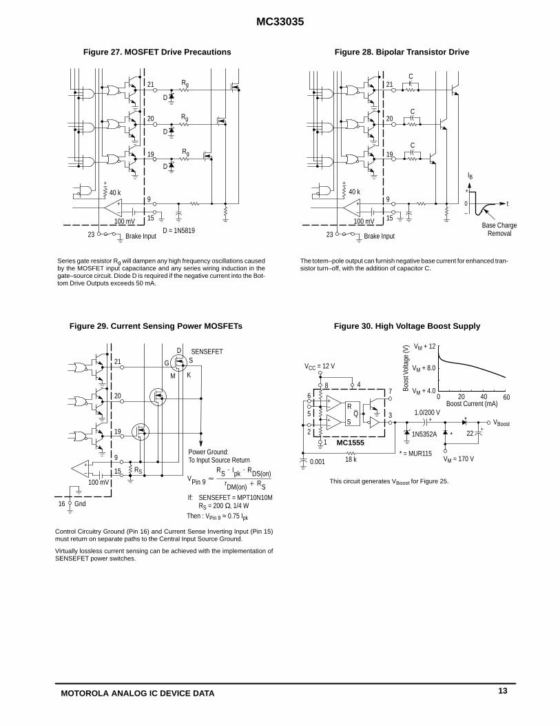
Figure 27. MOSFET Drive Precautions Figure 28. Bipolar Transistor Drive
t
+
0
–
IB
Base ChargeRemoval
C
C
C
Series gate resistor Rg will dampen any high frequency oscillations causedby the MOSFET input capacitance and any series wiring induction in thegate–source circuit. Diode D is required if the negative current into the Bot-tom Drive Outputs exceeds 50 mA.
The totem–pole output can furnish negative base current for enhanced tran-sistor turn–off, with the addition of capacitor C.
15
20
21
19
Brake Input23
9
D = 1N5819
40 k
100 mV
Rg
Rg
Rg
D
D
D
15
20
21
19
Brake Input23
940 k
100 mV
Figure 29. Current Sensing Power MOSFETs Figure 30. High Voltage Boost Supply
D
G S
RS
M K
SENSEFET
Virtually lossless current sensing can be achieved with the implementation ofSENSEFET power switches.
VPin 9RS Ipk RDS(on)
rDM(on) RS
Power Ground:To Input Source Return
If: SENSEFET = MPT10N10MRS = 200 Ω, 1/4 W
Then : VPin 9 ≈ 0.75 Ipk
16 Gnd
Control Circuitry Ground (Pin 16) and Current Sense Inverting Input (Pin 15)must return on separate paths to the Central Input Source Ground.
15
20
21
19
9
100 mV This circuit generates VBoost for Figure 25.
1.0/200 VVBoost
*
221
*1N5352AMC1555
5
2
6
0.001 18 k
3
VM + 12
VCC = 12 V
4
VM = 170 V
R
SQ
* = MUR115
8
Boost Current (mA)
VM + 4.040
76020
VM + 8.0
Boos
tVol
tage
(V)
0
MC33035
14 MOTOROLA ANALOG IC DEVICE DATA
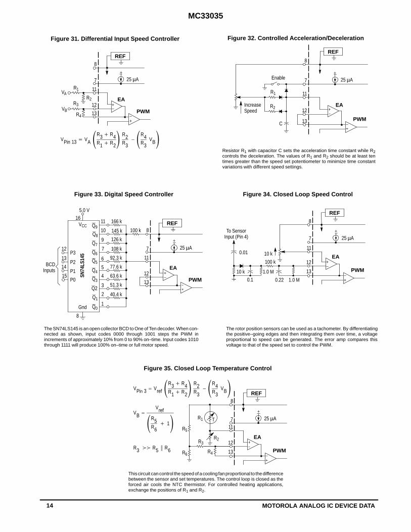
Figure 31. Differential Input Speed Controller Figure 32. Controlled Acceleration/Deceleration
R4
R2
R1
R3
13VB
VA
REF
PWM
EA
8
7
11
12
VPin 13 VA R3 R4R1 R2 R2
R3R4
R3VB
Resistor R1 with capacitor C sets the acceleration time constant while R2controls the deceleration. The values of R1 and R2 should be at least tentimes greater than the speed set potentiometer to minimize time constantvariations with different speed settings.
R1
EAR2
8
PWMC
Enable
IncreaseSpeed
7
12
11
13
REF
25 µA25 µA
PWM
EA
8
7
11
The SN74LS145 is an open collector BCD to One of Ten decoder. When con-nected as shown, input codes 0000 through 1001 steps the PWM inincrements of approximately 10% from 0 to 90% on–time. Input codes 1010through 1111 will produce 100% on–time or full motor speed.
Figure 33. Digital Speed Controller Figure 34. Closed Loop Speed Control
16VCC
Gnd Q0
2 40.4 k
8
P0
BCDInputs
Q9
Q8
Q7
Q6
Q5
Q4
Q3
Q2
Q1
P3
P2
P1
100 k
1
51.3 k3
4
5
6
7
63.6 k
77.6 k
92.3 k
108 k
9 126 k
11
145 k
166 k
10
5.0 V
SN74
LS14
5
REF
15
14
13
12 25 µA
13
12 13
REF
PWM
EA
8
7
11
12
The rotor position sensors can be used as a tachometer. By differentiatingthe positive–going edges and then integrating them over time, a voltageproportional to speed can be generated. The error amp compares thisvoltage to that of the speed set to control the PWM.
0.22
1.0 M
0.1
100 k
0.01
10 k
10 k
1.0 M
To SensorInput (Pin 4) 25 µA
13
REF
PWM
EA
8
711
12
This circuit can control the speed of a cooling fan proportional to the differencebetween the sensor and set temperatures. The control loop is closed as theforced air cools the NTC thermistor. For controlled heating applications,exchange the positions of R1 and R2.
Figure 35. Closed Loop Temperature Control
TR1
R6
R5
R2R3
R4
VB Vref
R5R6
1
R3 R5 R6
VPin 3 Vref R3 R4R1 R2 R2
R3R4
R3VB
25 µA
MC33035
15MOTOROLA ANALOG IC DEVICE DATA
SYSTEM APPLICATIONS
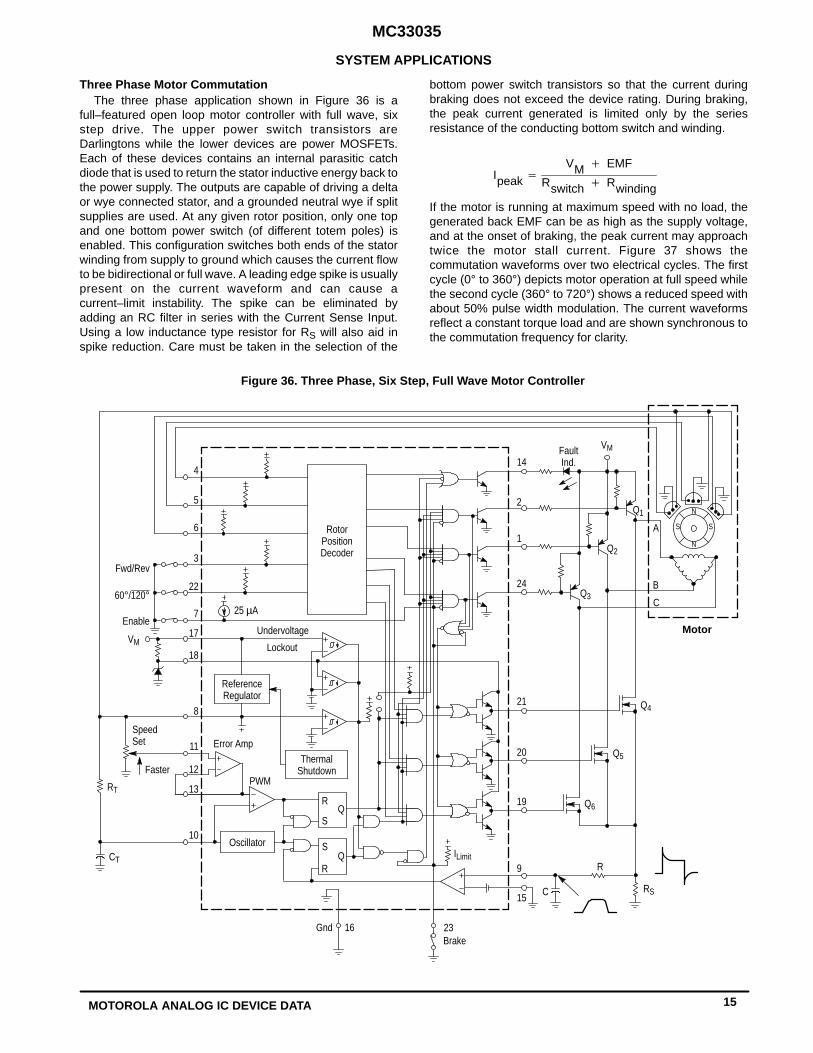
Three Phase Motor CommutationThe three phase application shown in Figure 36 is a
full–featured open loop motor controller with full wave, sixstep drive. The upper power switch transistors areDarlingtons while the lower devices are power MOSFETs.Each of these devices contains an internal parasitic catchdiode that is used to return the stator inductive energy back tothe power supply. The outputs are capable of driving a deltaor wye connected stator, and a grounded neutral wye if splitsupplies are used. At any given rotor position, only one topand one bottom power switch (of different totem poles) isenabled. This configuration switches both ends of the statorwinding from supply to ground which causes the current flowto be bidirectional or full wave. A leading edge spike is usuallypresent on the current waveform and can cause acurrent–limit instability. The spike can be eliminated byadding an RC filter in series with the Current Sense Input.Using a low inductance type resistor for RS will also aid inspike reduction. Care must be taken in the selection of the
bottom power switch transistors so that the current duringbraking does not exceed the device rating. During braking,the peak current generated is limited only by the seriesresistance of the conducting bottom switch and winding.
IpeakVM EMF
Rswitch Rwinding
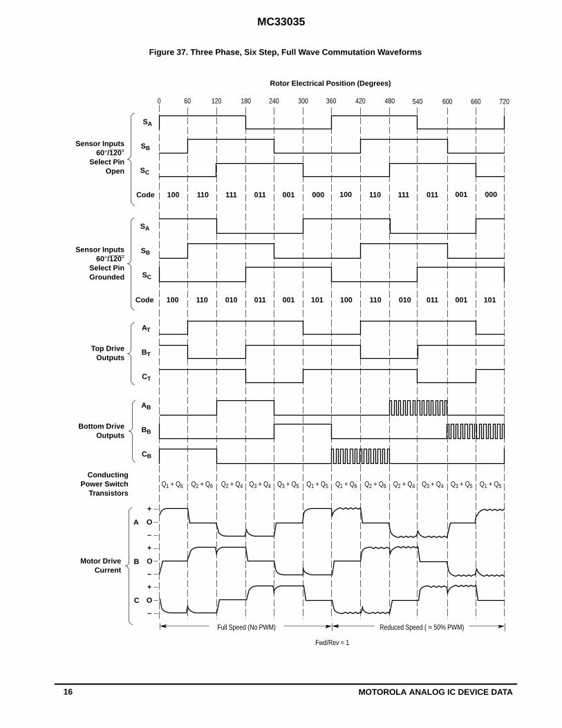
If the motor is running at maximum speed with no load, thegenerated back EMF can be as high as the supply voltage,and at the onset of braking, the peak current may approachtwice the motor stall current. Figure 37 shows thecommutation waveforms over two electrical cycles. The firstcycle (0° to 360°) depicts motor operation at full speed whilethe second cycle (360° to 720°) shows a reduced speed withabout 50% pulse width modulation. The current waveformsreflect a constant torque load and are shown synchronous tothe commutation frequency for clarity.
Figure 36. Three Phase, Six Step, Full Wave Motor Controller
RS
R
C
Q5
Q6
Q4
VM
S
Motor
A
Q3
S
C
B
Q1
Q2
Enable
QS
CT
RRT
Oscillator
Error Amp
PWM
ThermalShutdown
ReferenceRegulator
Lockout
UndervoltageVM
Fwd/Rev
QR
S
Faster
SpeedSet
RotorPositionDecoder
60°/120°
Brake
4
8
3
17
22
7
6
5
18
13
11
12
10
24
20
2
1
21
14
9
19
15
FaultInd.
Gnd 16 23
25 µA
ILimit
N
N
MC33035
16 MOTOROLA ANALOG IC DEVICE DATA
Figure 37. Three Phase, Six Step, Full Wave Commutation Waveforms
Rotor Electrical Position (Degrees)
100 000001011111110100000001011111110
720660600540480420360300240180120600
SA
SB
SC
Code
SC
SB
Code
SA
Sensor Inputs60°/120°
Select PinOpen
Sensor Inputs60°/120°
Select PinGrounded
AB
BB
Q2 + Q6
CB
Q2 + Q4 Q3 + Q4 Q3 + Q5 Q1 + Q5 Q1 + Q6
Bottom DriveOutputs
Q2 + Q6 Q2 + Q4 Q3 + Q4 Q3 + Q5
Motor DriveCurrent
B
Fwd/Rev = 1
C
–
O
+
–
O
+
ConductingPower Switch
TransistorsQ1 + Q5
Top DriveOutputs
Q1 + Q6
A
BT
AT
CT
–
O
+
100 110 001011 001011110100010 010 101101
Reduced Speed ( ≈ 50% PWM)Full Speed (No PWM)
MC33035
17MOTOROLA ANALOG IC DEVICE DATA
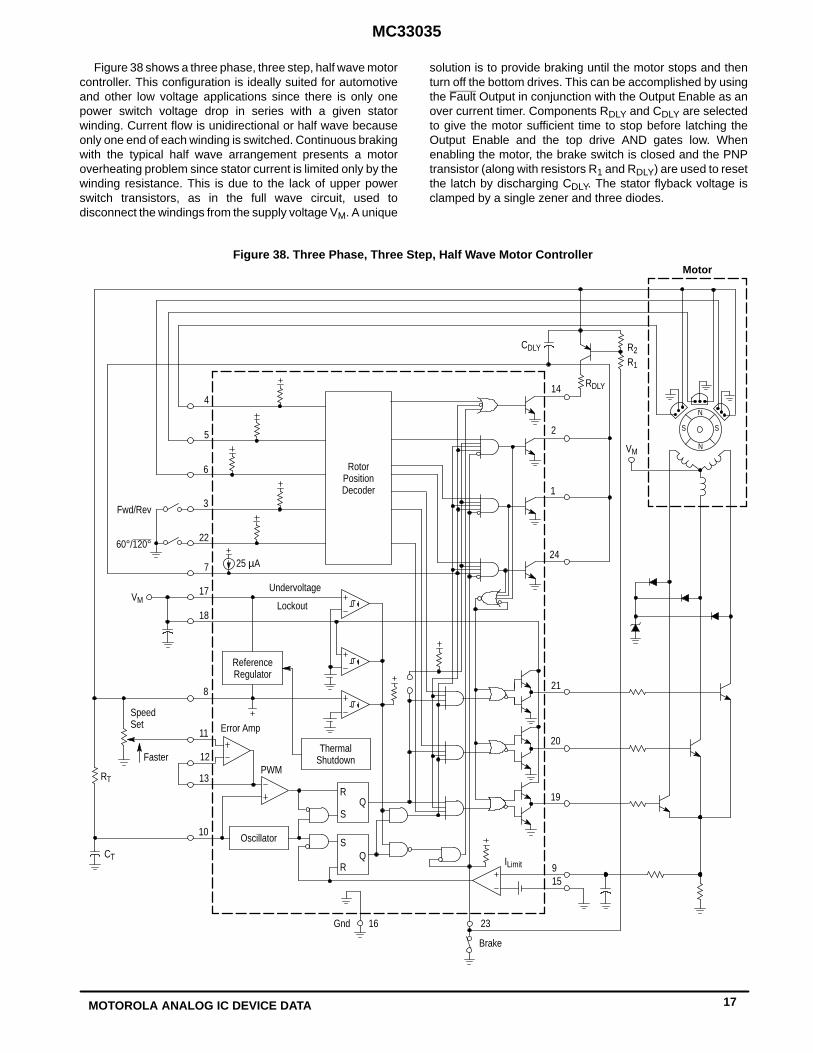
Figure 38 shows a three phase, three step, half wave motorcontroller. This configuration is ideally suited for automotiveand other low voltage applications since there is only onepower switch voltage drop in series with a given statorwinding. Current flow is unidirectional or half wave becauseonly one end of each winding is switched. Continuous brakingwith the typical half wave arrangement presents a motoroverheating problem since stator current is limited only by thewinding resistance. This is due to the lack of upper powerswitch transistors, as in the full wave circuit, used todisconnect the windings from the supply voltage VM. A unique
solution is to provide braking until the motor stops and thenturn off the bottom drives. This can be accomplished by usingthe Fault Output in conjunction with the Output Enable as anover current timer. Components RDLY and CDLY are selectedto give the motor sufficient time to stop before latching theOutput Enable and the top drive AND gates low. Whenenabling the motor, the brake switch is closed and the PNPtransistor (along with resistors R1 and RDLY) are used to resetthe latch by discharging CDLY. The stator flyback voltage isclamped by a single zener and three diodes.
Figure 38. Three Phase, Three Step, Half Wave Motor ControllerMotor
9
24
20
QS
CT
R
RT
Oscillator
Gnd
ILimit
Error Amp
PWM
ThermalShutdown
ReferenceRegulator
Lockout
UndervoltageVM
4
2
1
21
16
10
11
13
8
12
3
17
22
7
6
5
Fwd/Rev
QR
S
19
Faster
60°/120°
SS
VM
SpeedSet
RotorPositionDecoder
18
Brake
15
14
23
CDLY
RDLY
R2R1
25 µA
N
N
MC33035
18 MOTOROLA ANALOG IC DEVICE DATA
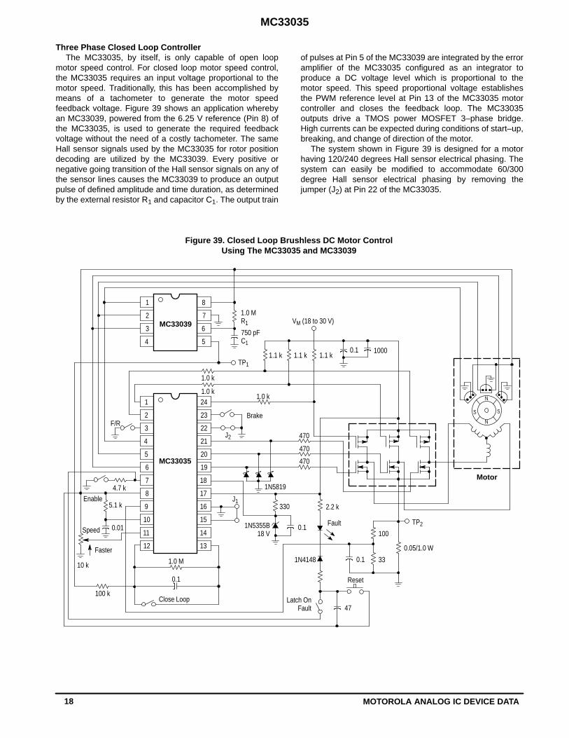
Three Phase Closed Loop ControllerThe MC33035, by itself, is only capable of open loop
motor speed control. For closed loop motor speed control,the MC33035 requires an input voltage proportional to themotor speed. Traditionally, this has been accomplished bymeans of a tachometer to generate the motor speedfeedback voltage. Figure 39 shows an application wherebyan MC33039, powered from the 6.25 V reference (Pin 8) ofthe MC33035, is used to generate the required feedbackvoltage without the need of a costly tachometer. The sameHall sensor signals used by the MC33035 for rotor positiondecoding are utilized by the MC33039. Every positive ornegative going transition of the Hall sensor signals on any ofthe sensor lines causes the MC33039 to produce an outputpulse of defined amplitude and time duration, as determinedby the external resistor R1 and capacitor C1. The output train
of pulses at Pin 5 of the MC33039 are integrated by the erroramplifier of the MC33035 configured as an integrator toproduce a DC voltage level which is proportional to themotor speed. This speed proportional voltage establishesthe PWM reference level at Pin 13 of the MC33035 motorcontroller and closes the feedback loop. The MC33035outputs drive a TMOS power MOSFET 3–phase bridge.High currents can be expected during conditions of start–up,breaking, and change of direction of the motor.
The system shown in Figure 39 is designed for a motorhaving 120/240 degrees Hall sensor electrical phasing. Thesystem can easily be modified to accommodate 60/300degree Hall sensor electrical phasing by removing thejumper (J2) at Pin 22 of the MC33035.
Figure 39. Closed Loop Brushless DC Motor ControlUsing The MC33035 and MC33039
Motor
TP2
0.05/1.0 W
0.1 33
TP1
1.0 k
VM (18 to 30 V)
10000.11.1 k
Close Loop
0.1
1.0 M
0.01Speed
Faster
4.7 k
F/RBrake
1.0 k
470
470
470
1N5819
1.1 k 1.1 k
1.0 k
1
2
3
4
8
7
6
5
1
2
3
4
9
5
6
7
8
10
24
23
22
21
20
19
18
17
16
15
MC33035
MC33039
1.0 MR1
750 pFC1
10 k
S S
J2
100 k
10011
12
14
13
5.1 kEnable J1
330
47
1N5355B18 V
2.2 k
0.1
1N4148
Latch OnFault
Fault
Reset
N
N
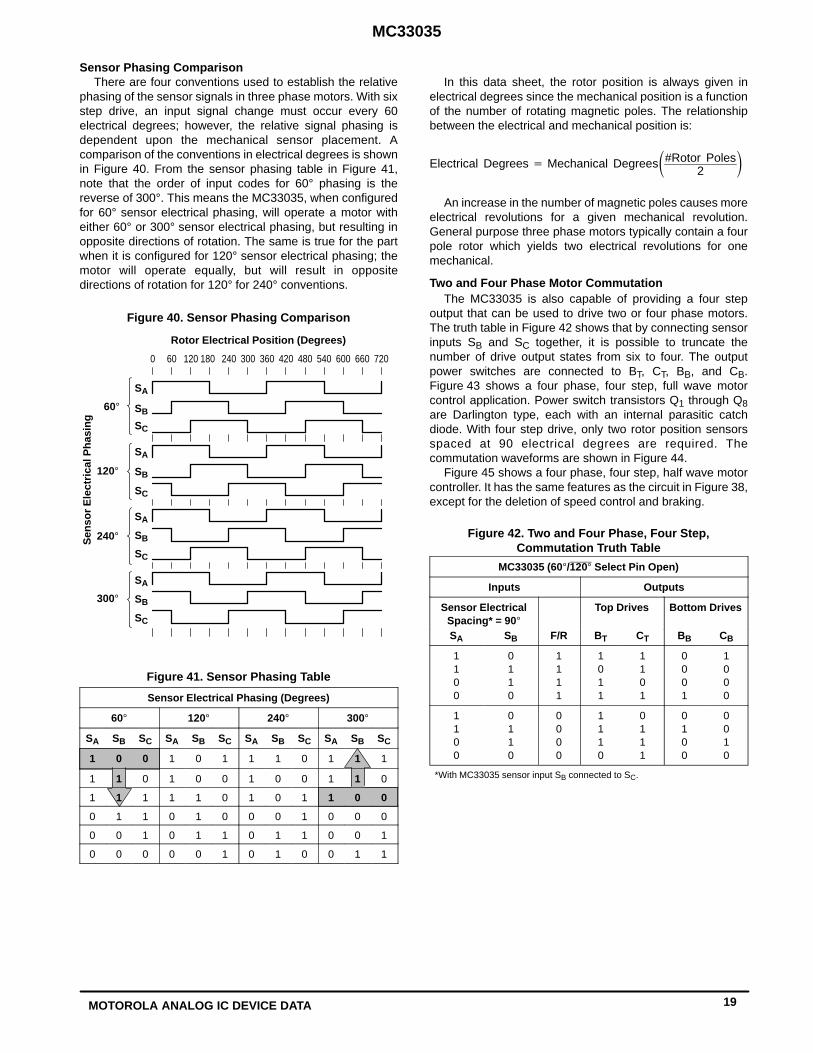
Figure 40. Sensor Phasing Comparison
Rotor Electrical Position (Degrees)
300°
240°
720660600540480420360300240180120600
SB
SA
120°
60°
SC
SA
SB
SC
SC
SB
SA
SC
SB
SA
Sen
sor E
lect
rical
Pha
sing
MC33035
19MOTOROLA ANALOG IC DEVICE DATA
Sensor Phasing ComparisonThere are four conventions used to establish the relative
phasing of the sensor signals in three phase motors. With sixstep drive, an input signal change must occur every 60electrical degrees; however, the relative signal phasing isdependent upon the mechanical sensor placement. Acomparison of the conventions in electrical degrees is shownin Figure 40. From the sensor phasing table in Figure 41,note that the order of input codes for 60° phasing is thereverse of 300°. This means the MC33035, when configuredfor 60° sensor electrical phasing, will operate a motor witheither 60° or 300° sensor electrical phasing, but resulting inopposite directions of rotation. The same is true for the partwhen it is configured for 120° sensor electrical phasing; themotor will operate equally, but will result in oppositedirections of rotation for 120° for 240° conventions.
Figure 41. Sensor Phasing Table
Sensor Electrical Phasing (Degrees)
60° 120° 240° 300°
SA SB SC SA SB SC SA SB SC SA SB SC
1 0 0 1 0 1 1 1 0 1 1 1
1 1 0 1 0 0 1 0 0 1 1 0
1 1 1 1 1 0 1 0 1 1 0 0
0 1 1 0 1 0 0 0 1 0 0 0
0 0 1 0 1 1 0 1 1 0 0 1
0 0 0 0 0 1 0 1 0 0 1 1
In this data sheet, the rotor position is always given inelectrical degrees since the mechanical position is a functionof the number of rotating magnetic poles. The relationshipbetween the electrical and mechanical position is:
Electrical Degrees Mechanical Degrees#Rotor Poles2
An increase in the number of magnetic poles causes moreelectrical revolutions for a given mechanical revolution.General purpose three phase motors typically contain a fourpole rotor which yields two electrical revolutions for onemechanical.
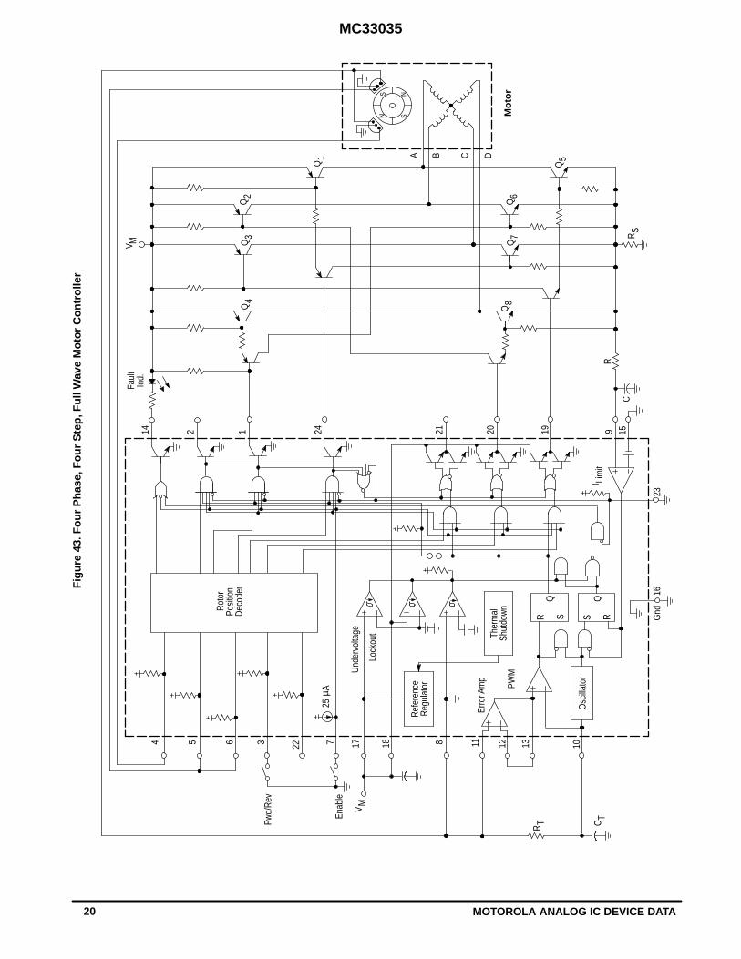
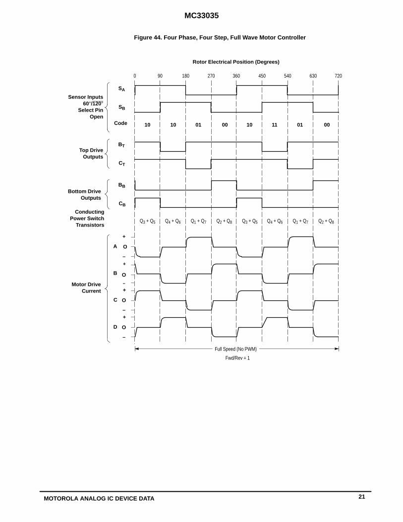
Two and Four Phase Motor CommutationThe MC33035 is also capable of providing a four step
output that can be used to drive two or four phase motors.The truth table in Figure 42 shows that by connecting sensorinputs SB and SC together, it is possible to truncate thenumber of drive output states from six to four. The outputpower switches are connected to BT, CT, BB, and CB.Figure 43 shows a four phase, four step, full wave motorcontrol application. Power switch transistors Q1 through Q8are Darlington type, each with an internal parasitic catchdiode. With four step drive, only two rotor position sensorsspaced at 90 electrical degrees are required. Thecommutation waveforms are shown in Figure 44.
Figure 45 shows a four phase, four step, half wave motorcontroller. It has the same features as the circuit in Figure 38,except for the deletion of speed control and braking.
Figure 42. Two and Four Phase, Four Step,Commutation Truth Table
MC33035 (60°/120° Select Pin Open)
Inputs Outputs
Sensor ElectricalSpacing* = 90 °
Top Drives Bottom Drives
SA SB F/R BT CT BB CB
1100
0110
1111
1011
1101
0001
1000
1100
0110
0000
1110
0111
0100
0010
*With MC33035 sensor input SB connected to SC.
MC33035
20 MOTOROLA ANALOG IC DEVICE DATA
Fig
ure
43. F
our
Pha
se, F
our
Ste
p, F
ull W
ave
Mot
or C
ontr
olle
r
CT
RT
VM
Enab
le
Fwd/
Rev
101312118177223654
91920
Lock
out
21
Rot
or
Und
ervo
ltage
241
Mot
or
2
Ref
eren
ce
Ther
mal
Osc
illato
r
Gnd
16
Q5Q1
Q2
Q6
Q7
Q3
Q4
Q8
V M
R
CR
S
Posi
tion
Dec
oder
Shut
dow
n
Reg
ulat
or
Erro
r Am
p
PWM
I Lim
it
SRQ
RSQ
A B DC
S
S
18
1514
23
25
Aµ
Faul
tIn
d.
N
N
MC33035
21MOTOROLA ANALOG IC DEVICE DATA
ConductingPower Switch
Transistors
A
SA
SB
Code
Q3 + Q5
Rotor Electrical Position (Degrees)
Fwd/Rev = 1
–
O
+
–
–
D
C
+
O
–
O
+
B
+
CB
O
BB
CT
BT
Q2 + Q8Q1 + Q7Q4 + Q6Q3 + Q5Q2 + Q8Q1 + Q7Q4 + Q6
0001111000011010
Motor DriveCurrent
Bottom DriveOutputs
Top DriveOutputs
Sensor Inputs60°/120°
Select PinOpen
180 270 360 450 540 630 7200 90
Figure 44. Four Phase, Four Step, Full Wave Motor Controller
Full Speed (No PWM)
MC33035
22 MOTOROLA ANALOG IC DEVICE DATA
R
Fig
ure
45. F
our
Pha
se, F
our
Ste
p, H
alf W
ave
Mot
or C
ontr
olle
r
VM
RS
Mot
or
SN
CT
RT
VM
Enab
le
Fwd/
Rev
101312118177223654
91920
Lock
out
21
Rot
or
Und
ervo
ltage
2412
Ref
eren
ce
Ther
mal
Osc
illato
r
Gnd
16
Posi
tion
Dec
oder
Shut
dow
n
Reg
ulat
or
Erro
r Am
p
PWM
I Lim
it
SRQ
RSQ
18
1514
23 Brak
e
25
Aµ
Faul
tIn
d.
C
NS
MC33035
23MOTOROLA ANALOG IC DEVICE DATA
Brush Motor ControlThough the MC33035 was designed to control brushless
DC motors, it may also be used to control DC brush typemotors. Figure 46 shows an application of the MC33035driving a MOSFET H–bridge affording minimal parts count tooperate a brush–type motor. Key to the operation is the inputsensor code [100] which produces a top–left (Q1) and abottom–right (Q3) drive when the controller’s forward/reversepin is at logic [1]; top–right (Q4), bottom–left (Q2) drive isrealized when the Forward/Reverse pin is at logic [0]. Thiscode supports the requirements necessary for H–bridgedrive accomplishing both direction and speed control.
The controller functions in a normal manner with a pulsewidth modulated frequency of approximately 25 kHz. Motorspeed is controlled by adjusting the voltage presented to thenoninverting input of the error amplifier establishing thePWM’s slice or reference level. Cycle–by–cycle currentlimiting of the motor current is accomplished by sensing thevoltage (100 mV) across the RS resistor to ground of theH–bridge motor current. The over current sense circuit makesit possible to reverse the direction of the motor, using the
normal forward/reverse switch, on the fly and not have tocompletely stop before reversing.
LAYOUT CONSIDERATIONSDo not attempt to construct any of the brushless
motor control circuits on wire–wrap or plug–in prototypeboards. High frequency printed circuit layout techniques areimperative to prevent pulse jitter. This is usually caused byexcessive noise pick–up imposed on the current sense orerror amp inputs. The printed circuit layout should contain aground plane with low current signal and high drive andoutput buffer grounds returning on separate paths back to thepower supply input filter capacitor VM. Ceramic bypasscapacitors (0.1 µF) connected close to the integrated circuit at VCC, VC, Vref and the erroramp noninverting input may be required depending uponcircuit layout. This provides a low impedance path for filteringany high frequency noise. All high current loops should bekept as short as possible using heavy copper runs tominimize radiated EMI.
9
24
20
QS
0.005
R
10 k
Oscillator
Gnd
ILimit
Error Amp
PWM
ThermalShutdown
ReferenceRegulator
Lockout
Undervoltage+12 V
4
2
1
21
16
10
11
13
8
12
3
17
22
7
6
5
Fwd/Rev
QR
S
19
Faster
RotorPositionDecoder
18
Brake
15
14
23
25 µA
Figure 46. H–Bridge Brush–Type Controller
RS
1.0 k
0.001
22
22
DC BrushMotor
M
+12 V
1.0 k
1.0 k
Q1*
Q2*
Q4*
Q3*
Enable
10 k
FaultInd.
20 k
MC33035
24 MOTOROLA ANALOG IC DEVICE DATA
P SUFFIXPLASTIC PACKAGE
CASE 724–03ISSUE D
DW SUFFIXPLASTIC PACKAGE
CASE 751E–04(SO–24L)ISSUE E
OUTLINE DIMENSIONS
MIN MINMAX MAXINCHES MILLIMETERS
DIM1.2650.2700.1750.020
0.060
0.0120.140
15° 0.040
0.050 BSC
0.100 BSC
0.300 BSC
1.27 BSC
2.54 BSC
7.62 BSC
ABCDEFGJKLMN
31.256.353.690.38
1.02
0.182.80
0° 0.51
32.136.854.440.51
1.52
0.303.55
15° 1.01
1.2300.2500.1450.015
0.040
0.0070.110
0° 0.020
NOTES:1. CHAMFERED CONTOUR OPTIONAL.2. DIMENSION L TO CENTER OF LEADS WHEN
FORMED PARALLEL.3. DIMENSIONING AND TOLERANCING PER ANSI
Y14.5M, 1982.4. CONTROLLING DIMENSION: INCH.
1 12
1324
-A-
-B-
C
K
N
-T-SEATINGPLANE
GE
F
D 24 PL
J 24 PL
M
NOTE 1
L
0.25 (0.010) T AM M
0.25 (0.010) T BM M
T0.010 (0.25) A BM S SMIN MINMAX MAX
MILLIMETERS INCHESDIM
ABCDFGJKMPR
15.257.402.350.350.41
0.230.13
0° 10.050.25
15.547.602.650.490.90
0.320.29
8° 10.550.75
0.6010.2920.0930.0140.016
0.0090.005
0° 0.3950.010
0.6120.2990.1040.0190.035
0.0130.011
8° 0.4150.029
1.27 BSC 0.050 BSC
NOTES:1. DIMENSIONING AND TOLERANCING PER ANSI
Y14.5M, 1982.2. CONTROLLING DIMENSION: MILLIMETER.3. DIMENSIONS A AND B DO NOT INCLUDE
MOLD PROTRUSION.4. MAXIMUM MOLD PROTRUSION 0.15 (0.006)
PER SIDE.5. DIMENSION D DOES NOT INCLUDE DAMBAR
PROTRUSION. ALLOWABLE DAMBARPROTRUSION SHALL BE 0.13 (0.005) TOTAL INEXCESS OF D DIMENSION AT MAXIMUMMATERIAL CONDITION.
-A-
-B-
1 12
24 13
-T-
C
KSEATINGPLANE
R X 45°
G 22 PL
P 12 PL
0.010 (0.25) BM M
F
J
M
D 24 PL
OUTLINE DIMENSIONS
Motorola reserves the right to make changes without further notice to any products herein. Motorola makes no warranty, representation or guarantee regardingthe suitability of its products for any particular purpose, nor does Motorola assume any liability arising out of the application or use of any product or circuit, andspecifically disclaims any and all liability, including without limitation consequential or incidental damages. “Typical” parameters which may be provided in Motoroladata sheets and/or specifications can and do vary in different applications and actual performance may vary over time. All operating parameters, including “Typicals”must be validated for each customer application by customer’s technical experts. Motorola does not convey any license under its patent rights nor the rights ofothers. Motorola products are not designed, intended, or authorized for use as components in systems intended for surgical implant into the body, or otherapplications intended to support or sustain life, or for any other application in which the failure of the Motorola product could create a situation where personal injuryor death may occur. Should Buyer purchase or use Motorola products for any such unintended or unauthorized application, Buyer shall indemnify and hold Motorolaand its officers, employees, subsidiaries, affiliates, and distributors harmless against all claims, costs, damages, and expenses, and reasonable attorney feesarising out of, directly or indirectly, any claim of personal injury or death associated with such unintended or unauthorized use, even if such claim alleges thatMotorola was negligent regarding the design or manufacture of the part. Motorola and are registered trademarks of Motorola, Inc. Motorola, Inc. is an EqualOpportunity/Affirmative Action Employer.
Mfax is a trademark of Motorola, Inc.How to reach us:USA/EUROPE/Locations Not Listed : Motorola Literature Distribution; JAPAN : Nippon Motorola Ltd.: SPD, Strategic Planning Office, 4–32–1,P.O. Box 5405, Denver, Colorado 80217. 303–675–2140 or 1–800–441–2447 Nishi–Gotanda, Shinagawa–ku, Tokyo 141, Japan. 81–3–5487–8488
Mfax : [email protected] – TOUCHTONE 602–244–6609 ASIA/PACIFIC : Motorola Semiconductors H.K. Ltd.; 8B Tai Ping Industrial Park,– US & Canada ONLY 1–800–774–1848 51 Ting Kok Road, Tai Po, N.T., Hong Kong. 852–26629298
INTERNET: http://motorola.com/sps
MC33035/D◊