iso14xx 5-kvrms isolated rs-485/rs-422 transceiver with
TRANSCRIPT

MCU
GND1
Logic Supply
Galvanic Isolation
Barrier
VDD
DGND
Logic Ground
RE
VCC1
D
R
VCC2
B
TI Isolated
TransceiverA
GND2
RS485 Bus
Bus-Side Supply
Isolated Ground
DE
Product
Folder
Order
Now
Technical
Documents
Tools &
Software
Support &Community
An IMPORTANT NOTICE at the end of this data sheet addresses availability, warranty, changes, use in safety-critical applications,intellectual property matters and other important disclaimers. UNLESS OTHERWISE NOTED, this document contains PRODUCTIONDATA.
ISO1410, ISO1412, ISO1430, ISO1432ISO1450, ISO1452
SLLSF22G –APRIL 2018–REVISED JUNE 2020
ISO14xx 5-kVRMS Isolated RS-485/RS-422 Transceiverwith Robust EMC
1
1 Features1• Compatible with TIA/EIA-485-A• PROFIBUS compatible at 5-V bus-side supply• Bus I/O protection
– ± 30 kV HBM– ±16 kV IEC 61000-4-2 Contact discharge– ± 4 kV IEC 61000-4-4 Electrical fast transient
• Low-EMI 500-kbps, 12 Mbps and 50 Mbps DataRates
• 1.71-V to 5.5-V logic-side supply (VCC1), 3-V to5.5-V bus-side supply (VCC2)
• Failsafe receiver for bus open, short, and idle• 1/8 Unit load up to 256 nodes on bus• 100-kV/µs (typical) high common-mode transient
immunity• Extended temperature range from –40°C to
+125°C• Glitch-free power-up and power-down for hot plug-
in• Wide-body SOIC-16 package• Pin compatible to most isolated RS-485
transceivers• Safety-related certifications:
– 7071-VPK VIOTM and 1500-VPK VIORM(reinforced and basic options) per DIN VDE V0884-11:2017-01
– 5000-VRMS isolation for 1 minute per UL 1577– IEC 60950-1, IEC 62368-1, IEC 60601-1 and
IEC 61010-1 certifications– CQC, TUV, and CSA approvals
2 Applications• Grid infrastructure• Solar inverter• Factory automation & control• Motor drives• HVAC systems and building automation
3 DescriptionThe ISO14xx devices are galvanically-isolateddifferential line transceivers for TIA/EIA RS-485 andRS-422 applications. These noise-immunetransceivers are designed to operate in harshindustrial environments. The bus pins of thesedevices can endure high levels of IEC electrostaticdischarge (ESD) and IEC electrical fast transient(EFT) events which eliminates the need for additionalcomponents on bus for system-level protection. Thedevices are available for both basic and reinforcedisolation (see Reinforced and Basic IsolationOptions).
Device Information(1)
PART NUMBER PACKAGE BODY SIZE (NOM)ISO1410, ISO1410B
SOIC (16) 10.30 mm × 7.50 mm
ISO1412, ISO1412BISO1430, ISO1430BISO1432, ISO1432BISO1450, ISO1450BISO1452, ISO1452B
(1) For all available packages, see the orderable addendum atthe end of the data sheet.
Reinforced and Basic Isolation OptionsFeature ISO14xx ISO14xxB
Protection level Reinforced BasicSurge test voltage perVDE 10000 VPK 6000 VPK
Isolation rating per UL 5000 VRMS 5000VRMS
Working voltage per VDE 1060 VRMS /1500 VPK
1060 VRMS /1500 VPK
Simplified Application Schematic
2
ISO1410, ISO1412, ISO1430, ISO1432ISO1450, ISO1452SLLSF22G –APRIL 2018–REVISED JUNE 2020 www.ti.com
Product Folder Links: ISO1410 ISO1412 ISO1430 ISO1432 ISO1450 ISO1452
Submit Documentation Feedback Copyright © 2018–2020, Texas Instruments Incorporated
Table of Contents1 Features .................................................................. 12 Applications ........................................................... 13 Description ............................................................. 14 Revision History..................................................... 25 Description Continued .......................................... 46 Device Options....................................................... 47 Pin Configuration and Functions ......................... 58 Specifications......................................................... 7
8.1 Absolute Maximum Ratings ...................................... 78.2 ESD Ratings.............................................................. 78.3 Recommended Operating Conditions....................... 78.4 Thermal Information .................................................. 88.5 Power Ratings........................................................... 88.6 Insulation Specifications............................................ 98.7 Safety-Related Certifications................................... 108.8 Safety Limiting Values ............................................ 108.9 Electrical Characteristics: Driver ............................. 118.10 Electrical Characteristics: Receiver ...................... 118.11 Supply Current Characteristics: Side 1 (ICC1) ....... 138.12 Supply Current Characteristics: Side 2 (ICC2) ....... 148.13 Switching Characteristics: Driver .......................... 158.14 Switching Characteristics: Receiver...................... 158.15 Insulation Characteristics Curves ......................... 16
8.16 Typical Characteristics .......................................... 179 Parameter Measurement Information ................ 2310 Detailed Description ........................................... 26
10.1 Overview ............................................................... 2610.2 Functional Block Diagram ..................................... 2610.3 Feature Description............................................... 2710.4 Device Functional Modes...................................... 28
11 Application and Implementation........................ 3111.1 Application Information.......................................... 3111.2 Typical Application ................................................ 32
12 Power Supply Recommendations ..................... 3513 Layout................................................................... 35
13.1 Layout Guidelines ................................................. 3513.2 Layout Example .................................................... 36
14 Device and Documentation Support ................. 3714.1 Documentation Support ........................................ 3714.2 Related Links ........................................................ 3714.3 Receiving Notification of Documentation Updates 3714.4 Community Resource............................................ 3714.5 Trademarks ........................................................... 3714.6 Electrostatic Discharge Caution............................ 3714.7 Glossary ................................................................ 38
15 Mechanical, Packaging, and OrderableInformation ........................................................... 38
4 Revision HistoryNOTE: Page numbers for previous revisions may differ from page numbers in the current version.
Changes from Revision F (February 2020) to Revision G Page
• Added minimum driver rise/fall time specification of 240 ns to 8.13 Switching characteristics: Driver (500kbps devices).. 15
Changes from Revision E (October 2019) to Revision F Page
• Added updated certification information in Safety-Related Certifications............................................................................. 10
Changes from Revision D (May 2019) to Revision E Page
• Added footnote to Pin functions table for NC pins ................................................................................................................ 5
Changes from Revision C (April 2019) to Revision D Page
• Added B part numbers throughout datasheet ....................................................................................................................... 1
Changes from Revision B (November 2018) to Revision C Page
• Added ISO1430, ISO1432, ISO1450, ISO1452 in Device Information table ......................................................................... 1• Changed the position of Device Features tabels .................................................................................................................. 4• Added footnote to Pin Functions: Full-Duplex Device ............................................................................................................ 5• Added footnote to Pin Functions: Half-Duplex Device ........................................................................................................... 6• Added Typical curves for ISO143x and ISO145x in Typical Characteristics ...................................................................... 17
3
ISO1410, ISO1412, ISO1430, ISO1432ISO1450, ISO1452
www.ti.com SLLSF22G –APRIL 2018–REVISED JUNE 2020
Product Folder Links: ISO1410 ISO1412 ISO1430 ISO1432 ISO1450 ISO1452
Submit Documentation FeedbackCopyright © 2018–2020, Texas Instruments Incorporated
• Added Section 11.2.3 Application Curves and Section 11.2.3.1 Insulation Lifetime............................................................ 33
Changes from Revision A (August 2018) to Revision B Page
• Changed status to production data ....................................................................................................................................... 1
Changes from Original (July 2018) to Revision A Page
• Changed the designator of common mode voltage in Recommended operating condition to VI .......................................... 7• Added test condition for CMTI in Electrical characteristics: Driver ................................................................................... 11• Added test condition for CMTI in Electrical characteristics: Receiver .................................................................................. 12• Changed VTEST to VCM in the Common Mode Transient Immunity (CMTI)—Full Duplex and Common Mode Transient
Immunity (CMTI)—Half Duplex figures in the Parameter Measurement Information section .............................................. 23• Changed tPLH to tPZH and tPLZ to tPHZ in the first Driver Enable and Disable Times timing diagram in the Parameter
Measurement Information section ........................................................................................................................................ 24• Added tPHZ to the first Receiver Enable and Disable Times timing diagram in the Parameter Measurement
Information section .............................................................................................................................................................. 25
4
ISO1410, ISO1412, ISO1430, ISO1432ISO1450, ISO1452SLLSF22G –APRIL 2018–REVISED JUNE 2020 www.ti.com
Product Folder Links: ISO1410 ISO1412 ISO1430 ISO1432 ISO1450 ISO1452
Submit Documentation Feedback Copyright © 2018–2020, Texas Instruments Incorporated
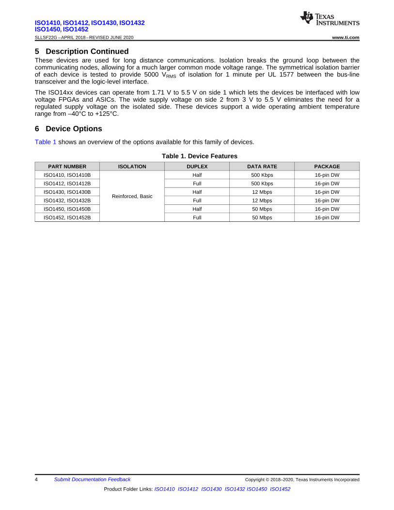
5 Description ContinuedThese devices are used for long distance communications. Isolation breaks the ground loop between thecommunicating nodes, allowing for a much larger common mode voltage range. The symmetrical isolation barrierof each device is tested to provide 5000 VRMS of isolation for 1 minute per UL 1577 between the bus-linetransceiver and the logic-level interface.
The ISO14xx devices can operate from 1.71 V to 5.5 V on side 1 which lets the devices be interfaced with lowvoltage FPGAs and ASICs. The wide supply voltage on side 2 from 3 V to 5.5 V eliminates the need for aregulated supply voltage on the isolated side. These devices support a wide operating ambient temperaturerange from –40°C to +125°C.
6 Device OptionsTable 1 shows an overview of the options available for this family of devices.
Table 1. Device FeaturesPART NUMBER ISOLATION DUPLEX DATA RATE PACKAGE
ISO1410, ISO1410B
Reinforced, Basic
Half 500 Kbps 16-pin DWISO1412, ISO1412B Full 500 Kbps 16-pin DWISO1430, ISO1430B Half 12 Mbps 16-pin DWISO1432, ISO1432B Full 12 Mbps 16-pin DWISO1450, ISO1450B Half 50 Mbps 16-pin DWISO1452, ISO1452B Full 50 Mbps 16-pin DW
1VCC1 16 VCC2
2GND1 15 GND2
3R 14 A
4RE 13 B
5DE 12 Z
6D 11 Y
7NC 10 NC
8GND1 9 GND2
Not to scale
ISO
LA
TIO
N
5
ISO1410, ISO1412, ISO1430, ISO1432ISO1450, ISO1452
www.ti.com SLLSF22G –APRIL 2018–REVISED JUNE 2020
Product Folder Links: ISO1410 ISO1412 ISO1430 ISO1432 ISO1450 ISO1452
Submit Documentation FeedbackCopyright © 2018–2020, Texas Instruments Incorporated
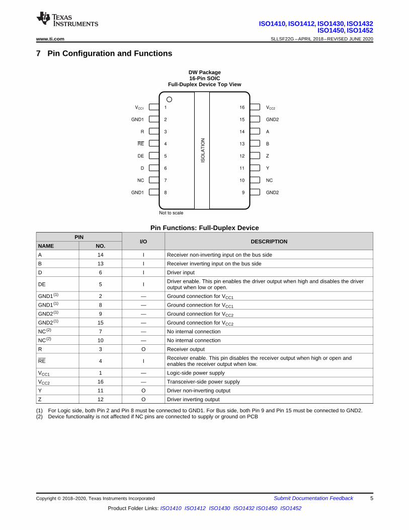
(1) For Logic side, both Pin 2 and Pin 8 must be connected to GND1. For Bus side, both Pin 9 and Pin 15 must be connected to GND2.(2) Device functionality is not affected if NC pins are connected to supply or ground on PCB
7 Pin Configuration and Functions
DW Package16-Pin SOIC
Full-Duplex Device Top View
Pin Functions: Full-Duplex DevicePIN
I/O DESCRIPTIONNAME NO.A 14 I Receiver non-inverting input on the bus sideB 13 I Receiver inverting input on the bus sideD 6 I Driver input
DE 5 I Driver enable. This pin enables the driver output when high and disables the driveroutput when low or open.
GND1 (1) 2 — Ground connection for VCC1
GND1 (1) 8 — Ground connection for VCC1
GND2 (1) 9 — Ground connection for VCC2
GND2 (1) 15 — Ground connection for VCC2
NC (2) 7 — No internal connectionNC (2) 10 — No internal connectionR 3 O Receiver output
RE 4 I Receiver enable. This pin disables the receiver output when high or open andenables the receiver output when low.
VCC1 1 — Logic-side power supplyVCC2 16 — Transceiver-side power supplyY 11 O Driver non-inverting outputZ 12 O Driver inverting output

1VCC1 16 VCC2
2GND1 15 GND2
3R 14 NC
4RE 13 B
5DE 12 A
6D 11 NC
7NC 10 NC
8GND1 9 GND2
Not to scaleIS
OL
AT
ION
6
ISO1410, ISO1412, ISO1430, ISO1432ISO1450, ISO1452SLLSF22G –APRIL 2018–REVISED JUNE 2020 www.ti.com
Product Folder Links: ISO1410 ISO1412 ISO1430 ISO1432 ISO1450 ISO1452
Submit Documentation Feedback Copyright © 2018–2020, Texas Instruments Incorporated
(1) For Logic side, both Pin 2 and Pin 8 must be connected to GND1. For Bus side, both Pin 9 and Pin 15 must be connected to GND2.(2) Device functionality is not affected if NC pins are connected to supply or ground on PCB
DW Package16-Pin SOIC
Half-Duplex Device Top View
Pin Functions: Half-Duplex DevicePIN
I/O DESCRIPTIONNAME NO.A 12 I/O Transceiver non-inverting input or output (I/O) on the bus sideB 13 I/O Transceiver inverting input or output (I/O) on the bus sideD 6 I Driver input
DE 5 I Driver enable. This pin enables the driver output when high and disables the driveroutput when low or open.
GND1 (1) 2 — Ground connection for VCC1
GND1 (1) 8 — Ground connection for VCC1
GND2 (1) 9 — Ground connection for VCC2
GND2 (1) 15 — Ground connection for VCC2
NC (2) 7 — No internal connectionNC (2) 10 — No internal connectionNC (2) 11 — No internal connectionNC (2) 14 — No internal connectionR 3 O Receiver output
RE 4 I Receiver enable. This pin disables the receiver output when high or open andenables the receiver output when low.
VCC1 1 — Logic-side power supplyVCC2 16 — Transceiver-side power supply
7
ISO1410, ISO1412, ISO1430, ISO1432ISO1450, ISO1452
www.ti.com SLLSF22G –APRIL 2018–REVISED JUNE 2020
Product Folder Links: ISO1410 ISO1412 ISO1430 ISO1432 ISO1450 ISO1452
Submit Documentation FeedbackCopyright © 2018–2020, Texas Instruments Incorporated
(1) Stresses beyond those listed under Absolute Maximum Ratings may cause permanent damage to the device. These are stress ratingsonly, which do not imply functional operation of the device at these or any other conditions beyond those indicated under RecommendedOperating Conditions. Exposure to absolute-maximum-rated conditions for extended periods may affect device reliability.
(2) All voltage values except differential I/O bus voltages are with respect to the local ground terminal (GND1 or GND2) and are peakvoltage values.
(3) Maximum voltage must not exceed 6 V
8 Specifications
8.1 Absolute Maximum RatingsOver operating free-air temperature range (unless otherwise noted) (1) (2)
MIN MAX UNITVCC1 Supply voltage, side 1 -0.5 6 VVCC2 Supply voltage, side 2 -0.5 6 VVIO Logic voltage level (D, DE, RE, R) -0.5 VCC1+0.5 (3) VIO Output current on R pin -15 15 mAVBUS Voltage on bus pins (A, B, Y, Z w.r.t GND2) -18 18 VTJ Junction temperature -40 150 TSTG Storage temperature -65 150
(1) JEDEC document JEP155 states that 500-V HBM allows safe manufacturing with a standard ESD control process.(2) JEDEC document JEP157 states that 250-V CDM allows safe manufacturing with a standard ESD control process.
8.2 ESD RatingsVALUE UNIT
V(ESD) Contact Discharge, per IEC 61000-4-2 Pins Bus terminals and GND2 ±16000 V
V(ESD) Contact Discharge, per IEC 61000-4-2 ISO141x, Pins Bus terminals and GND1(across isolation barrier) ±8000 V
V(ESD) Contact Discharge, per IEC 61000-4-2 ISO143x, Pins Bus terminals and GND1(across isolation barrier) ±8000 V
V(ESD)
Electrostatic dischargeHuman body model (HBM), perANSI/ESDA/JEDEC JS-001
All pins except bus pins (1) ±6000 V
Bus terminals to GND2 (1) ±30000
VElectrostatic dischargeCharged device model (CDM), perJEDEC specification JESD22-C101
All pins (2) ±1500
8.3 Recommended Operating ConditionsMIN MAX UNIT
VCC1Supply Voltage, Side 1, 1.8-V operation 1.71 1.89 VSupply Voltage, Side 1, 2.5-V, 3.3-V and 5.5-V operation 2.25 5.5 V
VCC2 Supply Voltage, Side 2 3 5.5 VVI Common Mode voltage at any bus terminal: A or B -7 12 VVIH High-level input voltage (D, DE, RE inputs) 0.7*Vcc1 Vcc1 VVIL Low-level input voltage (D, DE, RE inputs) 0 0.3*Vcc1 VVID Differential input voltage, A with respect to B -15 15 VIO Output current, Driver -60 60 mAIOR Output current, Receiver -4 4 mARL Differential load resistance 54 Ω
1/tUI Signaling rate ISO141x 500 kbps1/tUI Signaling Rate ISO143x 12 Mbps1/tUI Signaling rate ISO145x 50 MbpsTA Operating ambient temperature -40 125 °C

8
ISO1410, ISO1412, ISO1430, ISO1432ISO1450, ISO1452SLLSF22G –APRIL 2018–REVISED JUNE 2020 www.ti.com
Product Folder Links: ISO1410 ISO1412 ISO1430 ISO1432 ISO1450 ISO1452
Submit Documentation Feedback Copyright © 2018–2020, Texas Instruments Incorporated
(1) For more information about traditional and new thermal metrics, see the Semiconductor and IC Package Thermal Metrics applicationreport.
8.4 Thermal Information
THERMAL METRIC (1)ISO14xx
UNITDW (SOIC)16 PINS
RθJA Junction-to-ambient thermal resistance 67.9 °C/WRθJC(top) Junction-to-case (top) thermal resistance 27.7 °C/WRθJB Junction-to-board thermal resistance 29.4 °C/WψJT Junction-to-top characterization parameter 12.9 °C/WψJB Junction-to-board characterization parameter 28.8 °C/WRθJC(bot) Junction-to-case (bottom) thermal resistance — °C/W
8.5 Power RatingsPARAMETER TEST CONDITIONS MIN TYP MAX UNIT
ISO1410_ISO1412PD Maximum power dissipation (both sides) VCC1 = VCC2 = 5.5 V, TJ = 150°C, A-B
load = 54 Ω ||50pF, Load on R=15pFInput a 250kHz 50% duty cycle squarewave to D pin withVDE=VCC1, VRE=GND1
556 mWPD1 Maximum power dissipation (side-1) 28 mW
PD2 Maximum power dissipation (side-2) 528 mW
ISO1430_ISO1432PD Maximum power dissipation (both sides) VCC1 = VCC2 = 5.5 V, TJ = 150°C, A-B
load = 54 Ω ||50pF, Load on R=15pFInput a 6MHz 50% duty cycle squarewave to D pin withVDE=VCC1, VRE=GND1
352 mWPD1 Maximum power dissipation (side-1) 33 mW
PD2 Maximum power dissipation (side-2) 319 mW
ISO1450_ISO1452PD Maximum power dissipation (both sides) VCC1 = VCC2 = 5.5 V, TJ = 150°C, A-B
load = 54 Ω ||50pF, Load on R=15pFInput a 25MHz 50% duty cycle squarewave to D pin withVDE=VCC1, VRE=GND1
588 mWPD1 Maximum power dissipation (side-1) 49 mW
PD2 Maximum power dissipation (side-2) 539 mW
9
ISO1410, ISO1412, ISO1430, ISO1432ISO1450, ISO1452
www.ti.com SLLSF22G –APRIL 2018–REVISED JUNE 2020
Product Folder Links: ISO1410 ISO1412 ISO1430 ISO1432 ISO1450 ISO1452
Submit Documentation FeedbackCopyright © 2018–2020, Texas Instruments Incorporated
(1) Creepage and clearance requirements should be applied according to the specific equipment isolation standards of an application. Careshould be taken to maintain the creepage and clearance distance of a board design to ensure that the mounting pads of the isolator onthe printed-circuit board do not reduce this distance. Creepage and clearance on a printed-circuit board become equal in certain cases.Techniques such as inserting grooves, ribs, or both on a printed circuit board are used to help increase these specifications.
(2) ISO14xx is suitable for safe electrical insulation and ISO14xxB is suitable for basic electrical insulation only within the safety ratings.Compliance with the safety ratings shall be ensured by means of suitable protective circuits.
(3) Testing is carried out in air or oil to determine the intrinsic surge immunity of the isolation barrier.(4) Apparent charge is electrical discharge caused by a partial discharge (pd).(5) All pins on each side of the barrier tied together creating a two-pin device.
8.6 Insulation Specifications
PARAMETER TEST CONDITIONSSPECIFICATIONS
UNITDW-16
IEC 60664-1CLR External clearance (1) Side 1 to side 2 distance through air >8 mmCPG External creepage (1) Side 1 to side 2 distance across package surface >8 mmDTI Distance through the insulation Minimum internal gap (internal clearance) >17 µmCTI Comparative tracking index IEC 60112; UL 746A >600 V
Material Group According to IEC 60664-1 I
Overvoltage categoryRated mains voltage ≤ 600 VRMS I-IVRated mains voltage ≤ 1000 VRMS I-III
DIN VDE V 0884-11:2017-01 (2)
VIORM Maximum repetitive peak isolation voltage AC voltage (bipolar) 1500 VPK
VIOWM Maximum working isolation voltageAC voltage (sine wave); time-dependentdielectric breakdown (TDDB) test; see Figure 56 1060 VRMS
DC voltage 1500 VDC
VIOTM Maximum transient isolation voltage VTEST = VIOTM , t = 60 s (qualification); VTEST =1.2 × VIOTM, t = 1 s (100% production) 7071 VPK
VIOSM
Maximum surge isolation voltageISO141x (3)
Test method per IEC 62368-1, 1.2/50 µswaveform, VTEST = 1.6 × VIOSM = 10000 VPK(qualification)
6250 VPK
Maximum surge isolation voltageISO141xB (3)
Test method per IEC 62368-1, 1.2/50 µswaveform, VTEST = 1.3 × VIOSM = 6000 VPK(qualification)
4615 VPK
qpd Apparent charge (4)
Method a: After I/O safety test subgroup 2/3, Vini= VIOTM, tini = 60 s; Vpd(m) = 1.2 × VIORM , tm = 10s
≤ 5
pC
Method a: After environmental tests subgroup 1,Vini = VIOTM, tini = 60 s;ISO14xx: Vpd(m) = 1.6 × VIORM , tm = 10 sISO14xxB: Vpd(m) = 1.2 × VIORM , tm = 10 s
≤ 5
Method b1: At routine test (100% production)and preconditioning (type test), Vini = VIOTM, tini =1 s;ISO14xx: Vpd(m) = 1.875 × VIORM , tm = 1 sISO14xxB: Vpd(m) = 1.5 × VIORM , tm = 1 s
≤ 5
CIO Barrier capacitance, input to output (5) VIO = 0.4 × sin (2 πft), f = 1 MHz 1 pF
RIO Insulation resistance, input to output (5)
VIO = 500 V, TA = 25°C > 1012
ΩVIO = 500 V, 100°C ≤ TA ≤ 150°C > 1011
VIO = 500 V at TS = 150°C > 109
Pollution degree 2Climatic category 40/125/21
UL 1577
VISO Withstand isolation voltage VTEST = VISO , t = 60 s (qualification);VTEST = 1.2 × VISO , t = 1 s (100% production) 5000 VRMS
10
ISO1410, ISO1412, ISO1430, ISO1432ISO1450, ISO1452SLLSF22G –APRIL 2018–REVISED JUNE 2020 www.ti.com
Product Folder Links: ISO1410 ISO1412 ISO1430 ISO1432 ISO1450 ISO1452
Submit Documentation Feedback Copyright © 2018–2020, Texas Instruments Incorporated
8.7 Safety-Related CertificationsVDE CSA UL CQC TUV
Certified according to DINVDE V 0884-11:2017- 01
Certified according to IEC60950-1, IEC 62368-1and IEC 60601-1
Recognized under UL1577 ComponentRecognition Program
Certified according toGB4943.1-2011
Certified according to EN61010-1:2010/A1:2019,EN 60950-1:2006/A2:2013 and EN62368-1:2014
Maximum transientisolation voltage,7071 VPK;Maximum repetitive peakisolation voltage,1500 VPK;Maximum surge isolationvoltage,ISO141x, ISO143x,ISO145x: 6250 VPK(Reinforced)ISO141xB, ISO143xB,ISO145xB: 4600 VPK(Basic)
CSA 60950-1-07+A1+A2,IEC 60950-1 2ndEd.+A1+A2, CSA 62368-1-14, and IEC 62368-12nd Ed., for pollutiondegree 2, material group IISO141x, ISO143x,ISO145x: 800 VRMSreinforced isolationISO141xB, ISO143xB,ISO145xB: 800 VRMSbasic isolation----------------CSA 60601- 1:14 and IEC60601-1 Ed. 3.1,ISO141x, ISO143x,ISO145x: 2 MOPP(Means of PatientProtection) 250 VRMS (354VPK) maximum workingvoltage
Single protection,5000 VRMS
Reinforced insulation,Altitude ≤ 5000 m,Tropical Climate,700 VRMS maximumworking voltage
EN 61010-1:2010 /A1:2019ISO141x, ISO143x,ISO145x: 600 VRMSreinforced isolationISO141xB, ISO143xB,ISO145xB: 1000 VRMSbasic isolation----------------EN 60950-1:2006/A2:2013 and EN62368-1:2014ISO141x, ISO143x,ISO145x: 800 VRMSreinforced isolationISO141xB, ISO143xB,ISO145xB: 1060 VRMSbasic isolation
Reinforcedcertificate:40040142Basic certificate:40047657
Master contract number:220991 File number: E181974 Certificate number:
CQC15001121716 Client ID number: 77311
(1) The maximum safety temperature, TS, has the same value as the maximum junction temperature, TJ, specified for the device. The ISand PS parameters represent the safety current and safety power respectively. The maximum limits of IS and PS should not beexceeded. These limits vary with the ambient temperature, TA.The junction-to-air thermal resistance, RθJA, in the table is that of a device installed on a high-K test board for leaded surface-mountpackages. Use these equations to calculate the value for each parameter:TJ = TA + RθJA × P, where P is the power dissipated in the device.TJ(max) = TS = TA + RθJA × PS, where TJ(max) is the maximum allowed junction temperature.PS = IS × VI, where VI is the maximum input voltage.
8.8 Safety Limiting ValuesSafety limiting (1) intends to minimize potential damage to the isolation barrier upon failure of input or output circuitry.
PARAMETER TEST CONDITIONS MIN TYP MAX UNITDW-16 PACKAGE
IS Safety input, output, or supply current
RθJA = 67.9°C/W, VI = 5.5 V, TJ = 150°C,TA = 25°C, see Figure 1 334
mA
RθJA = 67.9°C/W, VI = 3.6 V, TJ = 150°C,TA = 25°C, see Figure 1 511
RθJA = 67.9°C/W, VI = 2.75 V, TJ =150°C, TA = 25°C, see Figure 1 669
RθJA = 67.9°C/W, VI = 1.89 V, TJ =150°C, TA = 25°C, see Figure 1 974
PS Safety input, output, or total power RθJA = 67.9°C/W, TJ = 150°C, TA = 25°C,see Figure 2 1837 mW
TS Maximum safety temperature 150 °C

11
ISO1410, ISO1412, ISO1430, ISO1432ISO1450, ISO1452
www.ti.com SLLSF22G –APRIL 2018–REVISED JUNE 2020
Product Folder Links: ISO1410 ISO1412 ISO1430 ISO1432 ISO1450 ISO1452
Submit Documentation FeedbackCopyright © 2018–2020, Texas Instruments Incorporated
8.9 Electrical Characteristics: DriverAll typical specs are at VCC1=3.3V, VCC2=5V, TA=27°C, (Min/Max specs are over recommended operating conditions unlessotherwise noted)
PARAMETER TEST CONDITIONS MIN TYP MAX UNIT
|VOD| Driver differential-output voltagemagnitude
Open circuit voltage, unloaded bus,3 V ≤ VCC2 ≤ 5.5 V 1.5 5 VCC2 V
RL = 60 Ω, –7 V ≤ VTEST ≤ 12 V (see Figure 35), 3 V≤ VCC2 ≤ 3.6 V, TA<100C 1.5 2.3 V
RL = 60 Ω, –7 V ≤ VTEST ≤ 12 V (see Figure 35), 3.1V ≤ VCC2 ≤ 3.6 V, TA>100C 1.5 2.3
RL = 60 Ω, –7 V ≤ VTEST ≤ 12 V,4.5 V < VCC2 < 5.5 V (see Figure 35) 2.1 3.7 V
RL = 100 Ω (see Figure 36), RS-422 load 2 4.2 V
RL = 54 Ω (see Figure 36), RS-485 load, VCC2 = 3 Vto 3.6 V 1.5 2.3 V
RL = 54 Ω (see Figure 36), RS-485 load,4.5 V < VCC2 < 5.5 V 2.1 3.7 V
Δ|VOD| Change in differential output voltagebetween two states RL = 54 Ω or RL = 100 Ω, see Figure 36 –200 200 mV
VOC Common-mode output voltage RL = 54 Ω or RL = 100 Ω, see Figure 36 1 0.5 × VCC2 3 V
ΔVOC(SS)change in steady-state common-modeoutput voltage between two states RL = 54 Ω or RL = 100 Ω, see Figure 36 –200 200 mV
IOS Short-circuit output current
VD = VCC1 or VD = VGND1, VDE = VCC1, VCC2=3.3V ±10%–7 V ≤ V ≤ 12 V, see Figure 45
–250 250 mA
VD = VCC1 or VD = VGND1, VDE = VCC1, VCC2=5V ±10%–7 V ≤ V ≤ 12 V, see Figure 45
250 mA
Ii Input current VD and VDE = 0 V or VD and VDE = VCC1 –10 10 µA
CMTI Common-mode transient immunity VD=VCC1 or GND1, VCC1 = 1.71 V to 5.5 V, VCM =1200 V, ISO141x, See Figure 38 85 100 kV/µs
CMTI Common-mode transient immunity VD=VCC1 or GND1, VCC1 = 1.71 V to 5.5 V, VCM =1200 V, ISO143x, See Figure 38 85 100 kV/µs
CMTI Common-mode transient immunity VD=VCC1 or GND1, VCC1 = 2.25 V to 5.5 V, VCM =1200 V, ISO145x, See Figure 38 85 100 kV/µs
(1) Under any specific conditions, VTH+ is ensured to be at least Vhys higher than VTH–.
8.10 Electrical Characteristics: ReceiverAll typical specs are at VCC1=3.3V, VCC2=5V, TA=27°C, (Min/Max specs are over recommended operating conditions unlessotherwise noted)
PARAMETER TEST CONDITIONS MIN TYP MAX UNIT
Ii1 Bus input current VDE = 0 V, VCC2 = 0 V or VCC2 = 5.5 V, 500-kbpsdevices, VI = –7 V or VI = 12 V, other input at 0 V –100 125 µA
Ii1 Bus input currentVDE = 0 V, VCC2 = 0 V or VCC2 = 5.5 V, 12-Mbps and50-Mbps devices, VI = –7 V or VI = 12 V,other input at 0 V
–100 125 µA
Ii1 Bus input current VDE = 0 V, VCC2 = 0 V or VCC2 = 5.5 V, 500-kbpsdevices, VI = –15 V or VI = 15 V, other input at 0 V -200 125 µA
Ii1 Bus input currentVDE = 0 V, VCC2 = 0 V or VCC2 = 5.5 V, 12-Mbps and50-Mbps devices, VI = –15 V or VI = 15 V,other input at 0 V
-200 125 µA
VTH+ Positive-going input threshold voltage–15 V ≤ VCM ≤ 15 V See (1) -100 –10 mV
–7 V ≤ VCM ≤ 12 V See (1) -100 –20 mV
VTH–Negative-going input thresholdvoltage –15 V ≤ VCM ≤ 15 V –200 –130 See (1) mV
Vhys Input hysteresis (VTH+ – VTH–) –15 V ≤ VCM ≤ 15 V 30 mV
VOH Output high voltage on the R pin
VCC1=5V ± 10%, IOH = –4 mA, VID = 200 mV VCC1 – 0.4 V
VCC1=3.3V ± 10%, IOH = –2 mA, VID = 200 mV VCC1 – 0.3 V
VCC1=2.5V ± 10%, 1.8V+/-5%, IOH = –1 mA, VID =200 mV VCC1 – 0.2 V
12
ISO1410, ISO1412, ISO1430, ISO1432ISO1450, ISO1452SLLSF22G –APRIL 2018–REVISED JUNE 2020 www.ti.com
Product Folder Links: ISO1410 ISO1412 ISO1430 ISO1432 ISO1450 ISO1452
Submit Documentation Feedback Copyright © 2018–2020, Texas Instruments Incorporated
Electrical Characteristics: Receiver (continued)All typical specs are at VCC1=3.3V, VCC2=5V, TA=27°C, (Min/Max specs are over recommended operating conditions unlessotherwise noted)
PARAMETER TEST CONDITIONS MIN TYP MAX UNIT
VOL Output low voltage on the R pin
VCC1=5V ± 10%, IOL = 4 mA, VID = –200 mV 0.4 V
VCC1=3.3V ± 10%, IOL = 2 mA, VID = –200 mV 0.3 V
VCC1=2.5V ± 10%, 1.8V ± 5%, IOL = 1 mA, VID =–200 mV 0.2 V
IOZOutput high-impedance current onthe R pin VR = 0 V or VR = VCC1, VRE = VCC1 –1 1 µA
Ii Input current on the RE pin VRE = 0 V or VRE = VCC1 –10 10 µA
CMTI Common-mode transient immunity VCC1=1.71 V to 5.5 V, VID = 1.5 V or -1.5 V, VCM =1200 V, ISO141x, See Figure 38 85 100 kV/µs
CMTI Common-mode transient immunity VCC1=1.71 V to 5.5 V, VID = 1.5 V or -1.5 V, VCM =1200 V, ISO143x, See Figure 38 85 100 kV/µs
CMTI Common-mode transient immunity VCC1=2.25 V to 5.5 V, VID = 1.5 V or -1.5 V, VCM =1200 V, ISO145x, See Figure 38 85 100 kV/µs

13
ISO1410, ISO1412, ISO1430, ISO1432ISO1450, ISO1452
www.ti.com SLLSF22G –APRIL 2018–REVISED JUNE 2020
Product Folder Links: ISO1410 ISO1412 ISO1430 ISO1432 ISO1450 ISO1452
Submit Documentation FeedbackCopyright © 2018–2020, Texas Instruments Incorporated
(1) CL(R) is the load capacitance on the R pin.
8.11 Supply Current Characteristics: Side 1 (ICC1)Bus loaded or unloaded (over recommended operating conditions unless otherwise noted)PARAMETER TEST CONDITIONS MIN TYP MAX UNIT
DRIVER ENABLED, RECEIVER DISABLED
Logic-sidesupply current VD = VCC1, VCC1 = 5 V ± 10% 2.6 4.4 mA
Logic-sidesupply current VD = VCC1, VCC1 = 3.3 V ± 10% 2.6 4.4 mA
Logic-sidesupply current ISO141x, D = 500-kbps square wave with 50% duty cycle, VCC1 = 5 V ± 10% 3.2 5.1 mA
Logic-sidesupply current ISO141x, D = 500-kbps square wave with 50% duty cycle, VCC1 = 3.3 V ± 10% 3.2 5.1 mA
Logic-sidesupply current ISO143x, D = 12-Mbps square wave with 50% duty cycle, VCC1 = 5 V ± 10% 3.2 5.1 mA
Logic-sidesupply current ISO143x, D = 12-Mbps square wave with 50% duty cycle, VCC1 = 3.3 V ± 10% 3.2 5.1 mA
Logic-sidesupply current ISO145x, D = 50-Mbps square wave with 50% duty cycle, VCC1 = 5 V ± 10% 3.6 5.3 mA
Logic-sidesupply current ISO145x, D = 50-Mbps square wave with 50% duty cycle, VCC1 = 3.3 V ± 10% 3.4 5.2 mA
DRIVER ENABLED, RECEIVER ENABLED
Logic-sidesupply current VRE = VGND1, loopback if full-duplex device, VD = VCC1, VCC1 = 5 V ± 10% 2.6 4.4 mA
Logic-sidesupply current VRE = VGND1, loopback if full-duplex device, VD = VCC1, VCC1 = 3.3 V ± 10% 2.6 4.4 mA
Logic-sidesupply current
ISO141x, VRE = VGND1, loopback if full-duplex device, D = 500-kbps square wave with 50% duty cycle,VCC1 = 5 V ± 10%, CL(R)
(1) = 15 pF 3.3 5.1 mA
Logic-sidesupply current
ISO141x, VRE = VGND1, loopback if full-duplex device, D = 500-kbps square wave with 50% duty cycle,VCC1 = 3.3 V ± 10%, CL(R)
(1) = 15 pF 3.2 5.1 mA
Logic-sidesupply current
ISO143x, VRE = VGND1, loopback if full-duplex device, D = 12-Mbps square wave with 50% duty cycle,VCC1 = 5 V ± 10%, CL(R)
(1) = 15 pF 4.1 6 mA
Logic-sidesupply current
ISO143x, VRE = VGND1, loopback if full-duplex device, D= 12-Mbps square wave with 50% duty cycle,VCC1 = 3.3 V ± 10%, CL(R)
(1) = 15 pF 3.8 5.7 mA
Logic-sidesupply current
ISO145x, VRE = VGND1, loopback if full-duplex device, D = 50-Mbps square wave with 50% duty cycle,VCC1 = 5 V ± 10%, CL(R)
(1) = 15 pF 6.3 8.9 mA
Logic-sidesupply current
ISO145x, VRE = VGND1, loopback if full-duplex device, D= 50-Mbps square wave with 50% duty cycle,VCC1 = 3.3 V ± 10%, CL(R)
(1) = 15 pF 5.3 7.8 mA
DRIVER DISABLED, RECEIVER ENABLED
Logic-sidesupply current V(A-B) ≥ 200 mV, VD = VCC1, VCC1 = 5 V ± 10% 1.6 3.1 mA
Logic-sidesupply current V(A-B) ≥ 200 mV, VD = VCC1, VCC1 = 3.3 V ± 10% 1.6 3.1 mA
Logic-sidesupply current
ISO141x, (A-B) = 500-kbps square wave with 50% duty cycle, VD = VCC1, VCC1 = 5 V ± 10%, CL(R)(1) =
15 pF 1.7 3.1 mA
Logic-sidesupply current
ISO141x, (A-B) = 500-kbps square wave with 50% duty cycle, VD = VCC1, VCC1 = 3.3 V ± 10%, CL(R)(1)
= 15 pF 1.6 3.1 mA
Logic-sidesupply current
ISO143x, (A-B) = 12-Mbps square wave with 50% duty cycle, VD = VCC1, VCC1 = 5 V ± 10%, CL(R)(1) =
15 pF 2.6 4 mA
Logic-sidesupply current
ISO143x, (A-B) = 12-Mbps square wave with 50% duty cycle, VD = VCC1, VCC1 = 3.3 V ± 10%, CL(R)(1)
= 15 pF 2.2 3.7 mA
Logic-sidesupply current
ISO145x, (A-B) = 50-Mbps square wave with 50% duty cycle, VD = VCC1, VCC1 = 5 V ± 10%, CL(R)(1) =
15 pF 4.7 6.7 mA
Logic-sidesupply current
ISO145x, (A-B) = 50-Mbps square wave with 50% duty cycle, VD = VCC1, VCC1 = 3.3 V ± 10%, CL(R)(1)
= 15 pF 3.7 5.7 mA
DRIVER DISABLED, RECEIVER DISABLED
Logic-sidesupply current VDE = VGND1, VD = VCC1, VCC1 = 5 V ± 10% 1.6 3.1 mA
Logic-sidesupply current VDE = VGND1, VD = VCC1, VCC1 = 3.3 V ± 10% 1.6 3.1 mA

14
ISO1410, ISO1412, ISO1430, ISO1432ISO1450, ISO1452SLLSF22G –APRIL 2018–REVISED JUNE 2020 www.ti.com
Product Folder Links: ISO1410 ISO1412 ISO1430 ISO1432 ISO1450 ISO1452
Submit Documentation Feedback Copyright © 2018–2020, Texas Instruments Incorporated
8.12 Supply Current Characteristics: Side 2 (ICC2)VRE = VGND1 or VRE = VCC1 (over recommended operating conditions unless otherwise noted)PARAMETER TEST CONDITIONS MIN TYP MAX UNIT
DRIVER ENABLED, BUS UNLOADED
Bus-side supplycurrent VD = VCC1, VCC2 = 3.3 V ± 10% 4 6.1 mA
Bus-side supplycurrent VD = VCC1, VCC2 = 5 V ± 10% 4.5 6.6 mA
DRIVER ENABLED, BUS LOADED
Bus-side supplycurrent VD = VCC1, RL = 54 Ω, VCC2 = 3.3 V ± 10% 48 58 mA
Bus-side supplycurrent VD = VCC1, RL = 54 Ω, VCC2 = 5 V ± 10% 74 88 mA
Bus-side supplycurrent
ISO141x, D = 500-kbps square wave with 50% duty cycle, RL = 54 Ω, CL = 50 pF, VCC2 = 3.3 V ±10% 63 95 mA
Bus-side supplycurrent ISO141x, D = 500-kbps square wave with 50% duty cycle, RL = 54 Ω, CL = 50 pF, VCC2 = 5 V ± 10% 113 160 mA
Bus-side supplycurrent ISO143x, D = 12-Mbps square wave with 50% duty cycle, RL = 54 Ω, CL = 50 pF, VCC2 = 3.3 V ± 10% 56 75 mA
Bus-side supplycurrent ISO143x, D = 12-Mbps square wave with 50% duty cycle, RL = 54 Ω, CL = 50 pF, VCC2 = 5 V ± 10% 97 122 mA
Bus-side supplycurrent ISO145x, D = 50-Mbps square wave with 50% duty cycle, RL = 54 Ω, CL = 50 pF, VCC2 = 3.3 V ± 10% 84 103 mA
Bus-side supplycurrent ISO145x, D = 50-Mbps square wave with 50% duty cycle, RL = 54 Ω, CL = 50 pF, VCC2 = 5 V ± 10% 134 162 mA
DRIVER DISABLED, BUS LOADED OR UNLOADED
Bus-side supplycurrent VD = VCC1, VCC2 = 3.3 V ± 10% 2.6 4.3 mA
Bus-side supplycurrent VD = VCC1, VCC2 = 5 V ± 10% 2.8 4.5 mA
15
ISO1410, ISO1412, ISO1430, ISO1432ISO1450, ISO1452
www.ti.com SLLSF22G –APRIL 2018–REVISED JUNE 2020
Product Folder Links: ISO1410 ISO1412 ISO1430 ISO1432 ISO1450 ISO1452
Submit Documentation FeedbackCopyright © 2018–2020, Texas Instruments Incorporated
(1) Also known as pulse skew.
8.13 Switching Characteristics: DriverAll typical specs are at VCC1=3.3V, VCC2=5V, TA=27°C, (Min/Max specs are over recommended operating conditions unlessotherwise noted)
PARAMETER TEST CONDITIONS MIN TYP MAX UNIT500-kbps DEVICEStr, tf Differential output rise time and fall time RL = 54 Ω, CL = 50 pF, see Figure 37 240 460 680 nstPHL, tPLH Propagation delay RL = 54 Ω, CL = 50 pF, see Figure 37 310 570 nsPWD Pulse width distortion (1), |tPHL – tPLH| RL = 54 Ω, CL = 50 pF, see Figure 37 4 50 nstPHZ, tPLZ Disable time See Figure 40, and Figure 41 125 200 nstPZH, tPZL Enable time See Figure 40, and Figure 41 160 600 ns12-Mbps DEVICES
tr, tf Differential output rise time and fall time
RL = 54 Ω, CL = 50 pF, VCC2= 4.5 V to5.5 V, see Figure 37 10 25 ns
RL = 54 Ω, CL = 50 pF, VCC2= 3 V to 3.6V, see Figure 37 27.8 ns
tPHL, tPLH Propagation delay RL = 54 Ω, CL = 50 pF, see Figure 37 68 125 nsPWD Pulse width distortion (1), |tPHL – tPLH| RL = 54 Ω, CL = 50 pF, see Figure 37 2 10 nstPHZ, tPLZ Disable time See Figure 40, and Figure 41 75 125 nstPZH, tPZL Enable time See Figure 40, and Figure 41 75 160 ns50-Mbps DEVICES
tr, tf Differential output rise time and fall time
RL = 54 Ω, CL = 50 pF, VCC2= 4.5 V to5.5 V, see Figure 37 4.7 6 ns
RL = 54 Ω, CL = 50 pF, VCC2= 3 V to 3.6V, see Figure 37 7.8 ns
tPHL, tPLH Propagation delay RL = 54 Ω, CL = 50 pF, see Figure 37 19 41 nsPWD Pulse width distortion (1), |tPHL – tPLH| RL = 54 Ω, CL = 50 pF, see Figure 37 1 6 nstPHZ, tPLZ Disable time See Figure 40, and Figure 41 25 46 nstPZH, tPZL Enable time See Figure 40, and Figure 41 32 78 ns
(1) Also known as pulse skew.
8.14 Switching Characteristics: ReceiverAll typical specs are at VCC1=3.3V, VCC2=5V, TA=27°C, (Min/Max specs are over recommended operating conditions unlessotherwise noted)
PARAMETER TEST CONDITIONS MIN TYP MAX UNIT500-kbps DEVICEStr, tf Differential output rise time and fall time CL = 15 pF, see Figure 42 1 4 nstPHL, tPLH Propagation delay CL = 15 pF, see Figure 42 92 135 nsPWD Pulse width distortion (1), |tPHL – tPLH| CL = 15 pF, see Figure 42 4.5 12.5 nstPHZ, tPLZ Disable time See Figure 43 and Figure 44 9 30 nstPZH, tPZL Enable time See Figure 43 and Figure 44 5 20 ns12-Mbps DEVICEStr, tf Differential output rise time and fall time CL = 15 pF, see Figure 42 1 4 nstPHL, tPLH Propagation delay CL = 15 pF, see Figure 42 75 120 nsPWD Pulse width distortion (1), |tPHL – tPLH| CL = 15 pF, see Figure 42 1 10 nstPHZ, tPLZ Disable time See Figure 43 and Figure 44 9 30 nstPZH, tPZL Enable time See Figure 43 and Figure 44 5 20 ns50-Mbps DEVICEStr, tf Differential output rise time and fall time CL = 15 pF, see Figure 42 1 4 nstPHL, tPLH Propagation delay CL = 15 pF, see Figure 42 36 60 ns
Ambient Temperature (qC)
Safe
ty L
imitin
g C
urr
ent (m
A)
0 50 100 150 2000
200
400
600
800
1000
1200
D001
VCC = 1.89 VVCC = 2.75 VVCC = 3.6 VVCC = 5.5 V
Ambient Temperature (qC)
Safe
ty L
imitin
g P
ow
er
(mW
)
0 50 100 150 2000
500
1000
1500
2000
2500
d002
16
ISO1410, ISO1412, ISO1430, ISO1432ISO1450, ISO1452SLLSF22G –APRIL 2018–REVISED JUNE 2020 www.ti.com
Product Folder Links: ISO1410 ISO1412 ISO1430 ISO1432 ISO1450 ISO1452
Submit Documentation Feedback Copyright © 2018–2020, Texas Instruments Incorporated
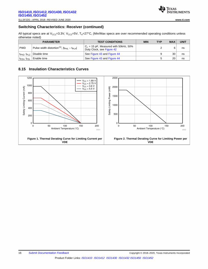
Switching Characteristics: Receiver (continued)All typical specs are at VCC1=3.3V, VCC2=5V, TA=27°C, (Min/Max specs are over recommended operating conditions unlessotherwise noted)
PARAMETER TEST CONDITIONS MIN TYP MAX UNIT
PWD Pulse width distortion (1), |tPHL – tPLH| CL = 15 pF, Measured with 50kHz, 50%Duty Clock, see Figure 42 2 6 ns
tPHZ, tPLZ Disable time See Figure 43 and Figure 44 9 30 nstPZH, tPZL Enable time See Figure 43 and Figure 44 5 20 ns
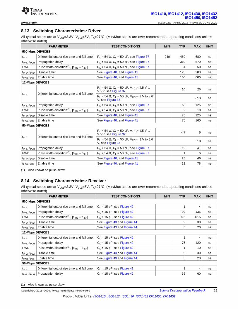
8.15 Insulation Characteristics Curves
Figure 1. Thermal Derating Curve for Limiting Current perVDE
Figure 2. Thermal Derating Curve for Limiting Power perVDE
Data rate (Mbps)
Supply
Curr
ent
(mA
)
0 2 4 6 8 10 120
10
20
30
40
50
60
70
80
90
100
d002
ICC1 (VCC1=3.3V)ICC2 (VCC2=3.3V)ICC2 (VCC2=5V)
Data rate (Mbps)
Supply
Curr
ent
(mA
)
0 2 4 6 8 10 120
20
40
60
80
100
120
d003
ICC1 (VCC1=3.3V)ICC2 (VCC2=3.3V)ICC2 (VCC2=5V)
Data rate (Mbps)
Supply
Curr
ent (m
A)
0 2 4 6 8 10 120
5
10
15
20
25
30
35
40
45
50
d001
ICC1 (VCC1=3.3V)ICC2 (VCC2=3.3V)ICC2 (VCC2=5V)
Data rate (kbps)
Supply
cu
rrent (m
A)
0 100 200 300 400 5000
10
20
30
40
50
60
70
80
90
D003
ICC1 (Vcc1=3.3V)ICC2 (Vcc2=3.3V)ICC2 (Vcc2=5V)
Data rate (kbps)
Supply
cu
rrent (m
A)
0 100 200 300 400 5000
10
20
30
40
50
60
70
D001
ICC1 (VCC1=3.3V)ICC2 (VCC2=3.3V)ICC2 (VCC2=5V)
Data rate (kbps)
Supply
cu
rrent (m
A)
0 100 200 300 400 5000
10
20
30
40
50
60
70
80
90
100
110
120
D002
ICC1 (VCC1=3.3V)ICC2 (VCC2=3.3V)ICC2 (VCC2=5V)
17
ISO1410, ISO1412, ISO1430, ISO1432ISO1450, ISO1452
www.ti.com SLLSF22G –APRIL 2018–REVISED JUNE 2020
Product Folder Links: ISO1410 ISO1412 ISO1430 ISO1432 ISO1450 ISO1452
Submit Documentation FeedbackCopyright © 2018–2020, Texas Instruments Incorporated
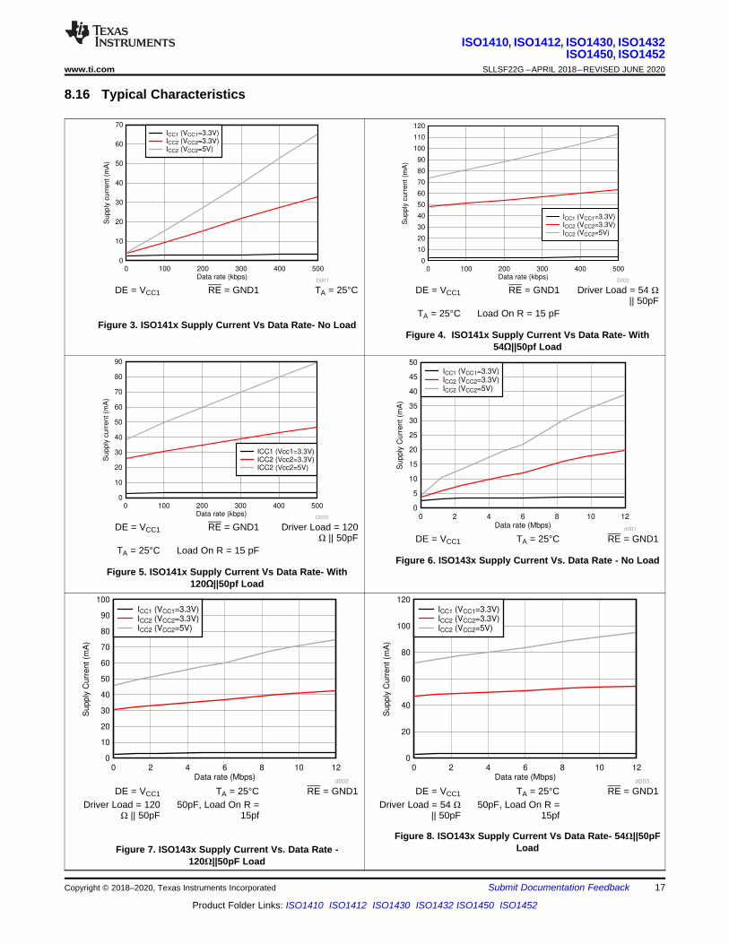
8.16 Typical Characteristics
DE = VCC1 RE = GND1 TA = 25°C
Figure 3. ISO141x Supply Current Vs Data Rate- No Load
DE = VCC1 RE = GND1 Driver Load = 54 Ω|| 50pF
TA = 25°C Load On R = 15 pF
Figure 4. ISO141x Supply Current Vs Data Rate- With54Ω||50pf Load
DE = VCC1 RE = GND1 Driver Load = 120Ω || 50pF
TA = 25°C Load On R = 15 pF
Figure 5. ISO141x Supply Current Vs Data Rate- With120Ω||50pf Load
DE = VCC1 TA = 25°C RE = GND1
Figure 6. ISO143x Supply Current Vs. Data Rate - No Load
DE = VCC1 TA = 25°C RE = GND1Driver Load = 120
Ω || 50pF50pF, Load On R =
15pf
Figure 7. ISO143x Supply Current Vs. Data Rate -120Ω||50pF Load
DE = VCC1 TA = 25°C RE = GND1Driver Load = 54 Ω
|| 50pF50pF, Load On R =
15pf
Figure 8. ISO143x Supply Current Vs Data Rate- 54Ω||50pFLoad

Driver output current (mA)
Drive
r diffe
rentia
l o
utp
ut
vo
lta
ge
(V
)
0 10 20 30 40 50 60 70 80 90 1001
1.5
2
2.5
3
3.5
4
4.5
5
D005Ambient temperature (qC)
Diffe
rentia
l ou
tpu
t vo
lta
ge
(V
)
-40 -20 0 20 40 60 80 100 120 1400
0.5
1
1.5
2
2.5
3
3.5
4
4.5
5
5.5
6
D006
VOD (3.3 V, 120 :)VOD (3.3 V, 54 :)VOD (5V, 120 :)VOD (5V, 54 :)
Ambient temp ( qC )
Driver
Ris
e/f
all
tim
e (
ns)
-40 -20 0 20 40 60 80 100 120 1404.75
4.8
4.85
4.9
4.95
5
5.05
5.1
5.15
5.2
5.25
5.3
5.35
d011
Driver output current (mA)
Drive
r ou
tpu
t vo
lta
ge
(V
)
0 10 20 30 40 50 60 70 80 90 1000
0.5
1
1.5
2
2.5
3
3.5
4
4.5
5
D004
VohVol
Data rate (Mbps)
Supply
Curr
ent
(mA
)
0 5 10 15 20 25 30 35 40 45 500
20
40
60
80
100
120
d009
ICC1 (VCC1=3.3V)ICC2 (VCC2=3.3V)ICC2 (VCC2=5V)
Data rate (Mbps)
Supply
Curr
ent
(mA
)
0 10 20 30 40 500
20
40
60
80
100
120
140
d010
ICC1 (VCC1=3.3V)ICC2 (VCC2=3.3V)ICC2 (VCC2=5V)
18
ISO1410, ISO1412, ISO1430, ISO1432ISO1450, ISO1452SLLSF22G –APRIL 2018–REVISED JUNE 2020 www.ti.com
Product Folder Links: ISO1410 ISO1412 ISO1430 ISO1432 ISO1450 ISO1452
Submit Documentation Feedback Copyright © 2018–2020, Texas Instruments Incorporated
Typical Characteristics (continued)
DE = VCC1 TA = 25°C RE = GND1
Figure 9. ISO145x Supply Current Vs Data Rate- No Load
DE = VCC1 TA = 25°C RE = GND1Driver Load = 120
Ω || 50pF50pF, Load On R =
15pf
Figure 10. ISO145x Supply Current Vs Data Rate-120Ω||50pF Load
DE = VCC1 TA = 25°C RE = GND1Driver Load = 54 Ω
|| 50pF50pF, Load On R =
15pf
Figure 11. ISO145x Supply Current Vs Data Rate- 54Ω||50pFLoad
DE = VCC1 D = GND1 VCC1 = 3.3 VTA = 25°C VCC2 = 5 V
Figure 12. Driver Output Voltage Vs Driver Output Current
DE = VCC1 D = GND1 VCC1 = 3.3 VTA = 25°C VCC2 = 5 V
Figure 13. Driver Differential Output Voltage Vs DriverOutput Current
Figure 14. Driver Differential Output Voltage Vs Temperature

Ambient temp ( qC )
Driver
Pro
pogation
De
lay (
ns)
-40 -20 0 20 40 60 80 100 120 14063.5
64
64.5
65
65.5
66
66.5
67
67.5
68
68.5
69
d005
Ambient temperature ( qC )
Drive
r pro
pa
ga
tio
n d
ela
y (
ns)
-40 -20 0 20 40 60 80 100 120 140300
305
310
315
320
325
330
335
340
345
350
D009
Ambient temp ( qC )
Driver
Ris
e/F
all
tim
e (
ns)
-40 -20 0 20 40 60 80 100 120 1407
7.5
8
8.5
9
9.5
d004Ambient temp ( qC )
Driver
Ris
e/f
all
tim
e (
ns)
-40 -20 0 20 40 60 80 100 120 1404.75
4.8
4.85
4.9
4.95
5
5.05
5.1
5.15
5.2
5.25
5.3
5.35
d011
Supply voltage VCC2 (V)
Drive
r o
utp
ut cu
rre
nt
(mA
)
0 0.5 1 1.5 2 2.5 3 3.5 4 4.5 5 5.50
10
20
30
40
50
60
70
80
D007D007Ambient temp ( qC )
Drive
r rise
/fa
ll tim
e (
ns)
-40 -20 0 20 40 60 80 100 120 140420
440
460
480
500
520
540
560
580
D008
19
ISO1410, ISO1412, ISO1430, ISO1432ISO1450, ISO1452
www.ti.com SLLSF22G –APRIL 2018–REVISED JUNE 2020
Product Folder Links: ISO1410 ISO1412 ISO1430 ISO1432 ISO1450 ISO1452
Submit Documentation FeedbackCopyright © 2018–2020, Texas Instruments Incorporated
Typical Characteristics (continued)
RL = 54 Ω DE = D = VCC1 TA = 25°C
Figure 15. Driver Output Current Vs Supply Voltage (VCC2)
VCC1 = 3.3 V VCC2 = 5 V
Figure 16. ISO141x Driver Rise/fall Time (ns) VsTemperature (c)
VCC1 = 3.3 V VCC2 = 5 V
Figure 17. ISO143x Driver Rise/Fall Time (ns) VsTemperature (C)
VCC1 = 3.3 V VCC2 = 5 V
Figure 18. ISO145x Driver Rise/Fall Time (ns) VsTemperature (C)
VCC1 = 3.3 V VCC2 = 5 V
Figure 19. ISO141x Driver Propagation Delay (ns) VsTemperature (c)
VCC1 = 3.3 V VCC2 = 5 V
Figure 20. ISO143x Driver Propagation Delay (ns) VsTemperature (C)

Ambient Temp ( qC)
Receiv
er
Pro
pog
ation d
ela
y (
ns)
-40 -20 0 20 40 60 80 100 120 14075
76
77
78
79
80
d006Ambient temperature ( qC )
Re
ce
ive
r P
ropo
ga
tio
n d
ela
y (
ns)
-40 -20 0 20 40 60 80 100 120 14037.5
38
38.5
39
39.5
40
40.5
41
41.5
42
42.5
43
43.5
44
44.5
d013
Low level output current (mA)
Lo
w leve
l o
utp
ut
vo
lta
ge
(V
)
0 2 4 6 8 10 12 14 160
0.1
0.2
0.3
0.4
0.5
0.6
0.7
0.8
D011
VOL (1.8V)VOL (3.3V)VOL((5V)
Ambient temperature ( qC )
Re
ce
ive
r p
rop
ag
atio
n d
ela
y (
ns)
-40 -20 0 20 40 60 80 100 120 14070
73
76
79
82
85
88
91
D012
Ambient temp ( qC )
Driver
Pro
pogation
dela
y (
ns)
-40 -20 0 20 40 60 80 100 12018
18.5
19
19.5
20
20.5
21
21.5
d012
High level output current (mA)
Hig
h le
ve
l o
utp
ut vo
lta
ge
(V
)
-15 -10 -5 00
0.5
1
1.5
2
2.5
3
3.5
4
4.5
5
D010
Voh (1.8V)Voh (3.3V)Voh (5V)
20
ISO1410, ISO1412, ISO1430, ISO1432ISO1450, ISO1452SLLSF22G –APRIL 2018–REVISED JUNE 2020 www.ti.com
Product Folder Links: ISO1410 ISO1412 ISO1430 ISO1432 ISO1450 ISO1452
Submit Documentation Feedback Copyright © 2018–2020, Texas Instruments Incorporated
Typical Characteristics (continued)
VCC1 = 3.3 V VCC2 = 5 V
Figure 21. ISO145x Driver Propagation Delay (ns) VsTemperature (C)
TA = 25° C
Figure 22. Receiver Buffer High Level Output Voltage VsHigh Level Output Current
TA = 25°C
Figure 23. Receiver Buffer Low Level Output Voltage VsLow Level Output Current
VCC1 = 3.3 V VCC2 = 5 V
Figure 24. ISO141x Receiver Propagation Delay (ns) VsTemperature (c)
VCC1 = 3.3 V VCC2 = 5 V
Figure 25. ISO143x Receiver Propagation Delay (ns) Vs.Temperature (C)
VCC1 = 3.3 V VCC2 = 5 V
Figure 26. ISO145x Receiver Propagation Delay (ns) Vs.Temperature (C)
Data Rate (Mbps)
VID
(m
V)
2 3 4 5 6 7 8 9 10 11 12200
250
300
350
400
450
500
550
600
d007Data Rate (Mbps)
Receiv
er
VID
(m
V)
0 5 10 15 20 25 30 35 40 45 50250
300
350
400
450
500
550
600
650
700
750
800
850
900
950
1000
1050
d014
21
ISO1410, ISO1412, ISO1430, ISO1432ISO1450, ISO1452
www.ti.com SLLSF22G –APRIL 2018–REVISED JUNE 2020
Product Folder Links: ISO1410 ISO1412 ISO1430 ISO1432 ISO1450 ISO1452
Submit Documentation FeedbackCopyright © 2018–2020, Texas Instruments Incorporated
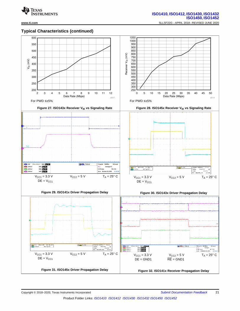
Typical Characteristics (continued)
For PWD ≤±5%
Figure 27. ISO143x Receiver VID vs Signaling Rate
For PWD ≤±5%
Figure 28. ISO145x Receiver VID vs Signaling Rate
VCC1 = 3.3 V VCC2 = 5 V TA = 25° CDE = VCC1
Figure 29. ISO141x Driver Propagation Delay
VCC1 = 3.3 V VCC2 = 5 V TA = 25° CDE = VCC1
Figure 30. ISO143x Driver Propagation Delay
VCC1 = 3.3 V VCC2 = 5 V TA = 25° CDE = VCC1
Figure 31. ISO145x Driver Propagation Delay
VCC1 = 3.3 V VCC2 = 5 V TA = 25° CDE = GND1 RE = GND1
Figure 32. ISO141x Receiver Propagation Delay

22
ISO1410, ISO1412, ISO1430, ISO1432ISO1450, ISO1452SLLSF22G –APRIL 2018–REVISED JUNE 2020 www.ti.com
Product Folder Links: ISO1410 ISO1412 ISO1430 ISO1432 ISO1450 ISO1452
Submit Documentation Feedback Copyright © 2018–2020, Texas Instruments Incorporated
Typical Characteristics (continued)
Figure 33. VCC1 Power Up/Power Down - Glitch FreeBehavior
Figure 34. VCC2 Power Up/Power Down - Glitch FreeBehavior
GND1
DEVCC1
GND1
+VOH or VOL
±
RE
R
GND1
Y
Z
+VOH or VOL
±
+ VCM ±
D
VCC2VCC1
A
B
1.5 V or 0 V
0 V or 1.5 V
GND2
54
54
10 µF
CL 15 pF(1)1 k
0.1 µF0.1 µF
10 µF
0 V
10%VOD (L)
VOD (H)
tftr
10%VOD
0 V90%
tPLHtPHL
VI
90%B or ZInput
Generator VI
D
GND1
CL(1)
50 pF ± 20%
RL
54 ± 1%
50
A or Y VOD
DE = VCC1
VCC1
50%
0 V or
VCC1
VOC
VOD
GND2
A or Y
D
B or Z
RL(1)
/ 2
RL(1)
/ 2
VOC(PP)
VOC
A
B
ûVOC(SS)
VA
VB
B or Z
D = 0 or
VCC1
DE = VCC1
VCC2
GND2
VOD
VTEST
+
±
375
375
RL
A or Y
23
ISO1410, ISO1412, ISO1430, ISO1432ISO1450, ISO1452
www.ti.com SLLSF22G –APRIL 2018–REVISED JUNE 2020
Product Folder Links: ISO1410 ISO1412 ISO1430 ISO1432 ISO1450 ISO1452
Submit Documentation FeedbackCopyright © 2018–2020, Texas Instruments Incorporated
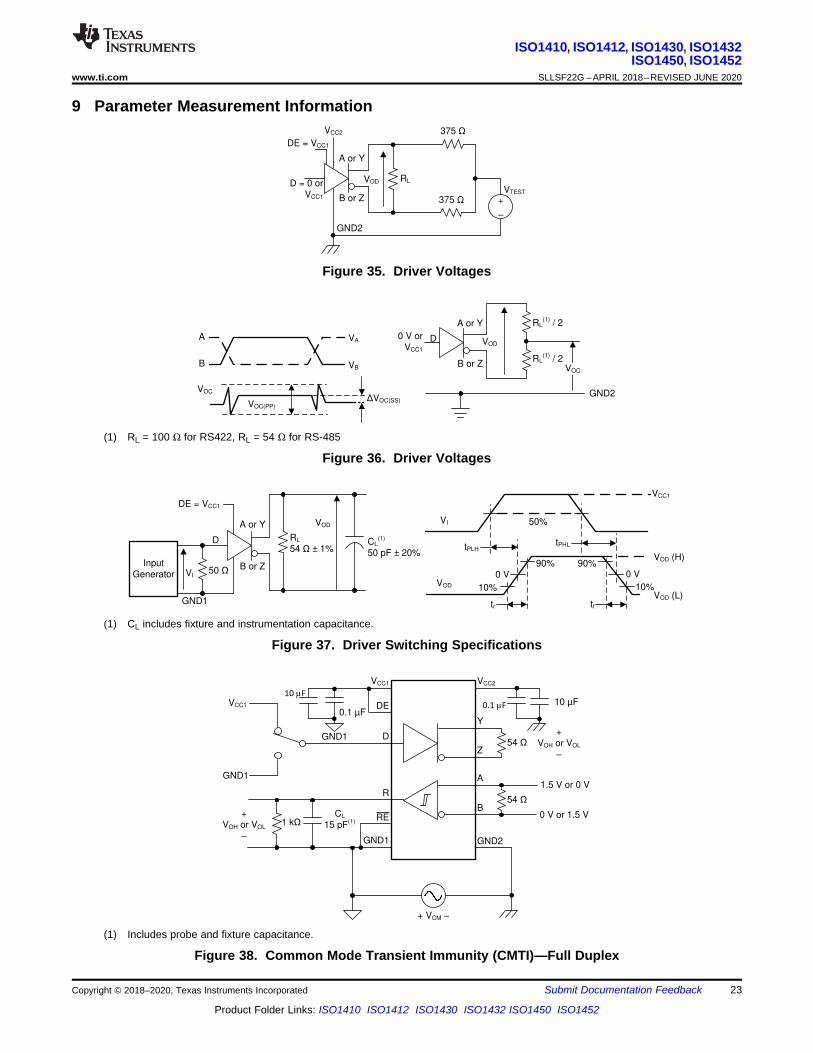
9 Parameter Measurement Information
Figure 35. Driver Voltages
(1) RL = 100 Ω for RS422, RL = 54 Ω for RS-485
Figure 36. Driver Voltages
(1) CL includes fixture and instrumentation capacitance.
Figure 37. Driver Switching Specifications
(1) Includes probe and fixture capacitance.
Figure 38. Common Mode Transient Immunity (CMTI)—Full Duplex

0 V
VOL
50%VO
tPLZ
50 % 50 %
tPZL
VI
10%
VCC2
A or Y
Input
Generator VI
GND1
DE
D
50
B or Z
S1
GND2
VCC2
VCC1
RL
110
CL(1)
50 pF
A or Y
Input
Generator VI
GND1
DE
VO
CL(1)
50 pFRL
110
§0 V
0 V
VOH
50%VO
tPHZ
50 % 50 %
VCC1
tPZH
VI
90%
D
50
B or Z
S1
GND2
GND1
DEVCC1
GND1
+VOH or VOL
±
RE
R
GND1
+VOH or VOL
±
+ VCM ±
D
VCC2VCC1
A
B
GND2
54
CL 15 pF(1)1 k
0.1 µF10 µF 10 µF0.1 µF
24
ISO1410, ISO1412, ISO1430, ISO1432ISO1450, ISO1452SLLSF22G –APRIL 2018–REVISED JUNE 2020 www.ti.com
Product Folder Links: ISO1410 ISO1412 ISO1430 ISO1432 ISO1450 ISO1452
Submit Documentation Feedback Copyright © 2018–2020, Texas Instruments Incorporated
Parameter Measurement Information (continued)
(1) Includes probe and fixture capacitance.
Figure 39. Common Mode Transient Immunity (CMTI)—Half Duplex
(1) CL includes fixture and instrumentation capacitance
Figure 40. Driver Enable and Disable Times
Figure 41. Driver Enable and Disable Times
C
Steady State
Logic Input
(1 or 0)
±7 9912 V
GND
A or Y
B or Z
I(1)G
V
G
C
A or Y
B or Z
Steady-State
Logic Input
(1 or 0)
GND
Input
Generator
VO
A
BR
RE
0 V or 1.5 V
VCC1
S11.5 V or 0 V
VI
1 k
CL
15 pF
50
VO
VI
50%
VCC1
§0 V
0 V
VOH
50%
VOL
VCC1
tPZL
VO
tPZH
A at 1.5 V
B at 0 V
S1 to GND
A at 0 V
B at 1.5 V
S1 to
VCC1
50%
VO
VI
50%
VCC1
§0 V
0 V
VOH
50%
VOL
VCC1
tPZL
VO
tPZH
50%
tPLZ
90%
10%
tPHZ
0 V
50 %
3 V
tPLH
VI
90%
10%
50%
tr tf
tPHL
VO
VOH
VOL
50%
50 %
Input
Generator
A
B1.5 V
RE
R VO
VI50 CL
(1)
15 pF
25
ISO1410, ISO1412, ISO1430, ISO1432ISO1450, ISO1452
www.ti.com SLLSF22G –APRIL 2018–REVISED JUNE 2020
Product Folder Links: ISO1410 ISO1412 ISO1430 ISO1432 ISO1450 ISO1452
Submit Documentation FeedbackCopyright © 2018–2020, Texas Instruments Incorporated
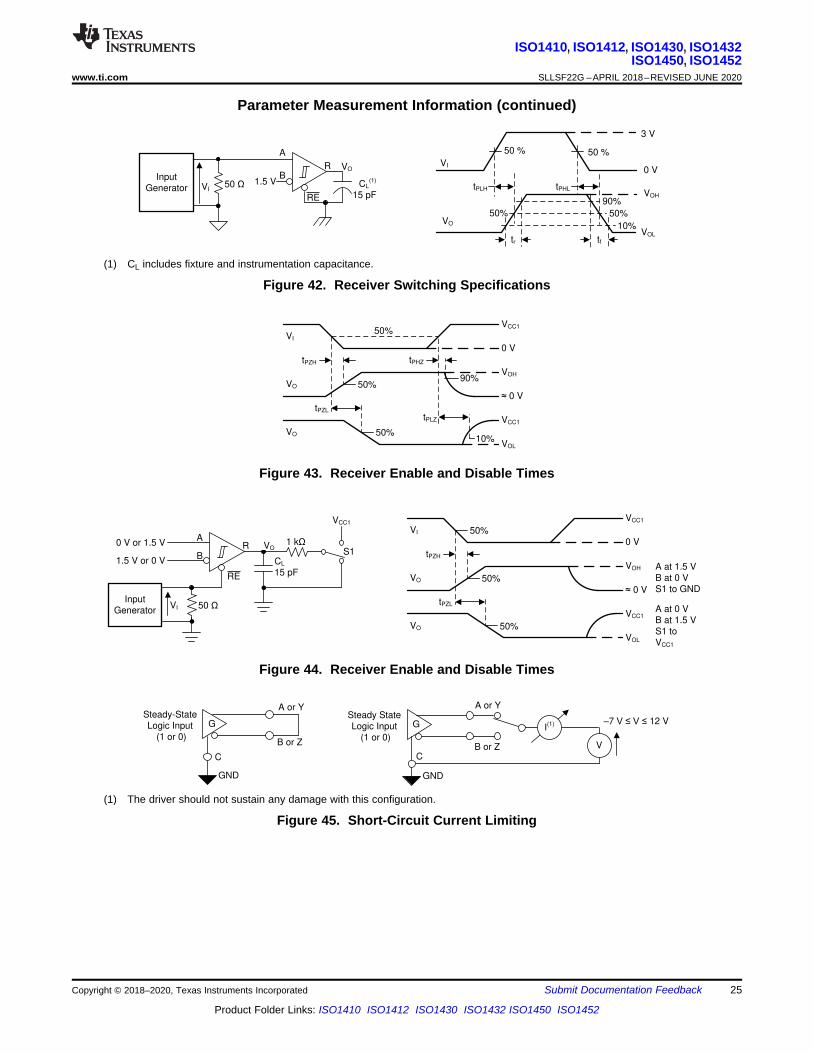
Parameter Measurement Information (continued)
(1) CL includes fixture and instrumentation capacitance.
Figure 42. Receiver Switching Specifications
Figure 43. Receiver Enable and Disable Times
Figure 44. Receiver Enable and Disable Times
(1) The driver should not sustain any damage with this configuration.
Figure 45. Short-Circuit Current Limiting

RE
Half duplex
VCC1
GND1
D Tx
R Rx
DE Tx
VCC2
Rx
Tx
Rx
GND2
VCC
GND2
VCC2
A
B
D
R
RE
Full duplex
VCC1
GND1
D Tx
R Rx
DE Tx
VCC2
Rx
Tx
Rx
GND2
VCC
GND2
VCC2
Y
B
D
R
Z
A
26
ISO1410, ISO1412, ISO1430, ISO1432ISO1450, ISO1452SLLSF22G –APRIL 2018–REVISED JUNE 2020 www.ti.com
Product Folder Links: ISO1410 ISO1412 ISO1430 ISO1432 ISO1450 ISO1452
Submit Documentation Feedback Copyright © 2018–2020, Texas Instruments Incorporated
10 Detailed Description
10.1 OverviewThe ISO14xx devices are isolated RS-485/RS-422 transceivers designed to operate in harsh industrialenvironments. ISO141x, ISO143x and ISO145x devices support up to 500 kbps, 12 Mbps and 50 Mbps signalingrates respectively. This family of devices has a 3-channel digital isolator and an RS-485 transceiver in a 16-pinwide-body SOIC package. The silicon-dioxide based capacitive isolation barrier supports an isolation withstandvoltage of 5 kVRMS and an isolation working voltage of 1500 VPK. Isolation breaks the ground loop between thecommunicating nodes and allows for data transfer in the presence of large ground potential differences. Thesedevices have a higher typical differential output voltage (VOD) than traditional transceivers for better noiseimmunity. A minimum differential output voltage of 2.1 V is specified at a VCC2 voltage of 5 V ±10% which meetsthe requirements for Profibus applications. The wide logic supply of the device (VCC1) supports interfacing with1.8-V, 2.5-V, 3.3-V, and 5-V control logic. The 3-V to 5.5-V bus side supply (VCC2) removes the need of a well-regulated isolated supply in end systems. Figure 46 shows the functional block diagram of the full-duplex devicesand Figure 47 shows the functional block diagram of a half-duplex devices.
10.2 Functional Block Diagram
Figure 46. Full-Duplex Block Diagram
Figure 47. Half-Duplex Block Diagram

VCC1
GND1
A
GND2
B
VCC2
Galvanic
Isolation Barrier
VCC2
RS-485
Bus
Traditional
transceiver
ISO
Ground
R2
RT
R1
VCC1
GND1
A
GND2
B
VCC2
Galvanic
Isolation Barrier
VCC2
RS-485
Bus
ISO1410
(R1 and R2 not needed)
ISO
Ground
RT
27
ISO1410, ISO1412, ISO1430, ISO1432ISO1450, ISO1452
www.ti.com SLLSF22G –APRIL 2018–REVISED JUNE 2020
Product Folder Links: ISO1410 ISO1412 ISO1430 ISO1432 ISO1450 ISO1452
Submit Documentation FeedbackCopyright © 2018–2020, Texas Instruments Incorporated
10.3 Feature Description
10.3.1 Electromagnetic Compatibility (EMC) ConsiderationsMany applications in harsh industrial environment are sensitive to disturbances such as electrostatic discharge(ESD), electrical fast transient (EFT), surge and electromagnetic emissions. These electromagnetic disturbancesare regulated by international standards such as IEC 61000-4-x and CISPR 22. Although system-levelperformance and reliability depends, to a large extent, on the application board design and layout, the ISO14xxdevices incorporate dedicated circuitry to protect the transceiver from ±16 kV ESD per IEC61000-4-2 and ±4 kVEFT per IEC 61000-4-4. System designers can achieve the ±4-kV EFT Criterion A with careful system design(data communication between nodes in the presence of transient noise with minimum to no data loss).
10.3.2 Failsafe ReceiverThe differential receiver of the ISO14xx devices has failsafe protection from invalid bus states caused by:• Open bus conditions such as a broken cable or a disconnected connector• Shorted bus conditions such as insulation breakdown of a cable that shorts the twisted-pair• Idle bus conditions that occur when no driver on the bus is actively driving
The differential input of the RS-485 receiver is 0 in any of these conditions for a terminated transmission line.The receiver outputs a failsafe logic-high state so that the output of the receiver is not indeterminate.
The receiver thresholds are offset in the receiver failsafe protection so that the indeterminate range of the doesnot include a 0 V differential. The receiver output must generate a logic high when the differential input (VID) isgreater than 200 mV to comply with the RS-485 standard. The receiver output must also generate a output alogic low when VID is less than –200 mV to comply with the RS-485 standard. The receiver parameters thatdetermine the failsafe performance are VTH+, VTH–, and VHYS. Differential signals less than –200 mV alwayscause a low receiver output as shown in the Electrical Characteristics table. Differential signals greater than 200mV always cause a high receiver output. A differential input signal that is near zero is still greater than the VTH+threshold which makes the receiver output logic high. The receiver output goes to a low state only when thedifferential input decreases by VHYS to less than VTH+.
The internal failsafe biasing feature removes the need for the two external resistors that are typically requiredwith traditional isolated RS-485 transceivers as shown in Figure 48.
Figure 48. Failsafe Transceiver
10.3.3 Thermal ShutdownThe ISO14xx devices have a thermal shutdown circuit to protect against damage when a fault condition occurs.A driver output short circuit or bus contention condition can cause the driver current to increase significantlywhich increases the power dissipation inside the device. An increase in the die temperature is monitored and thedevice is disabled when the die temperature becomes 170 (typical) which lets the device decrease thetemperature. The device is enabled when the junction temperature becomes 165 (typical).
28
ISO1410, ISO1412, ISO1430, ISO1432ISO1450, ISO1452SLLSF22G –APRIL 2018–REVISED JUNE 2020 www.ti.com
Product Folder Links: ISO1410 ISO1412 ISO1430 ISO1432 ISO1450 ISO1452
Submit Documentation Feedback Copyright © 2018–2020, Texas Instruments Incorporated
Feature Description (continued)
(1) PU = Powered Up; PD = Powered Down; H = High Level; L = Low level; X = Irrelevant, Hi-Z = High impedance state(2) The driver outputs are Y and Z for a full-duplex device. The driver outputs are A and B for a half-duplex device.(3) A strongly driven input signal can weakly power the floating VCC1 through an internal protection diode and cause an undetermined
output.
Bus short circuit for an extended duration and/or beyond voltage levels specified in recommended operatingcondition should be avoided. Repeated or prolonged exposure to bus shorts can result in high junctiontemperatures and affect device reliability.
10.3.4 Glitch-Free Power Up and Power DownCommunication on the bus that already exist between a master node and slave node in an RS485 network mustnot be disturbed when a new node is swapped in or out of the network. No glitches on the bus occur when thedevice is:• Hot plugged into the network in an unpowered state• Hot plugged into the network in a powered state and disabled state• Powered up or powered down in a disabled state when already connected to the bus
The ISO14xx devices do not cause any false data toggling on the bus when powered up or powered down in adisabled state with supply ramp rates from 100 µs to 10 ms.
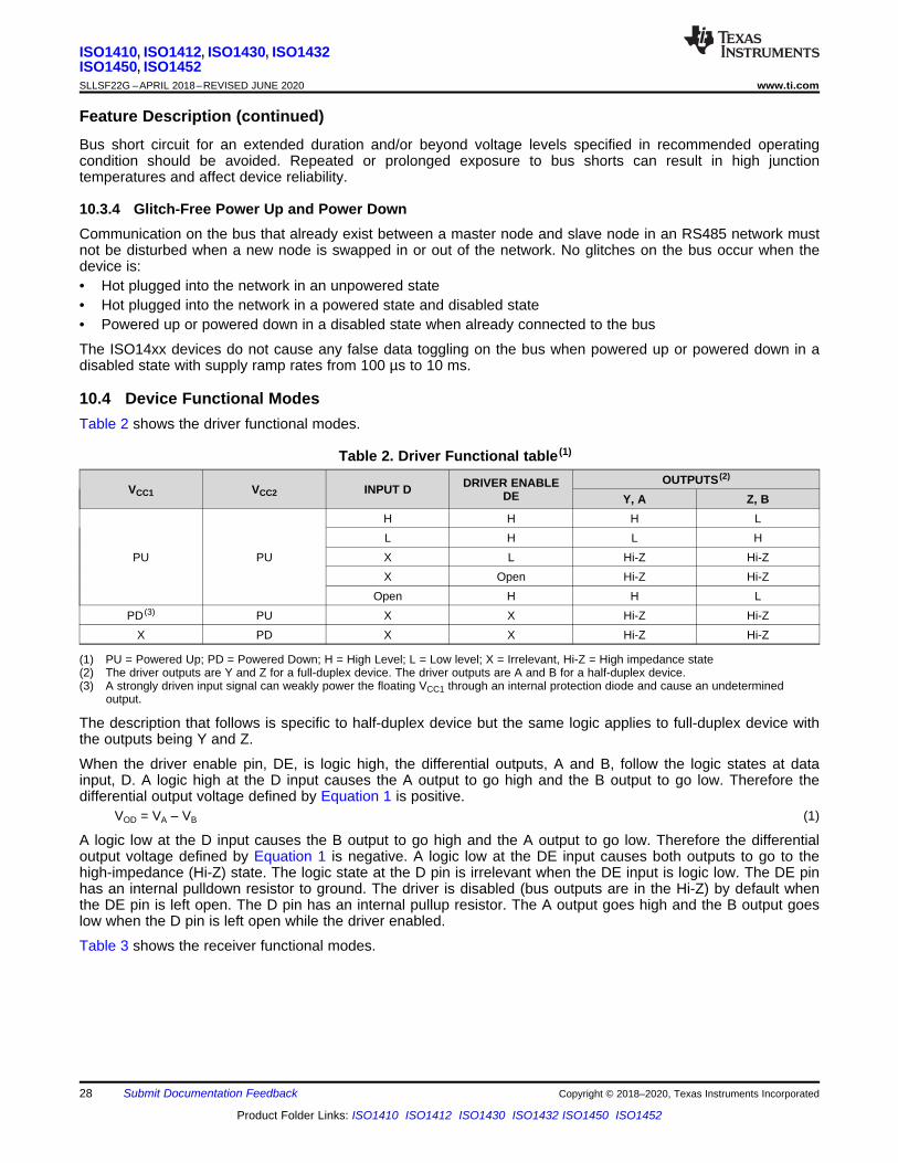
10.4 Device Functional ModesTable 2 shows the driver functional modes.
Table 2. Driver Functional table (1)
VCC1 VCC2 INPUT D DRIVER ENABLEDE
OUTPUTS (2)
Y, A Z, B
PU PU
H H H LL H L HX L Hi-Z Hi-ZX Open Hi-Z Hi-Z
Open H H LPD (3) PU X X Hi-Z Hi-Z
X PD X X Hi-Z Hi-Z
The description that follows is specific to half-duplex device but the same logic applies to full-duplex device withthe outputs being Y and Z.
When the driver enable pin, DE, is logic high, the differential outputs, A and B, follow the logic states at datainput, D. A logic high at the D input causes the A output to go high and the B output to go low. Therefore thedifferential output voltage defined by Equation 1 is positive.
VOD = VA – VB (1)
A logic low at the D input causes the B output to go high and the A output to go low. Therefore the differentialoutput voltage defined by Equation 1 is negative. A logic low at the DE input causes both outputs to go to thehigh-impedance (Hi-Z) state. The logic state at the D pin is irrelevant when the DE input is logic low. The DE pinhas an internal pulldown resistor to ground. The driver is disabled (bus outputs are in the Hi-Z) by default whenthe DE pin is left open. The D pin has an internal pullup resistor. The A output goes high and the B output goeslow when the D pin is left open while the driver enabled.
Table 3 shows the receiver functional modes.
29
ISO1410, ISO1412, ISO1430, ISO1432ISO1450, ISO1452
www.ti.com SLLSF22G –APRIL 2018–REVISED JUNE 2020
Product Folder Links: ISO1410 ISO1412 ISO1430 ISO1432 ISO1450 ISO1452
Submit Documentation FeedbackCopyright © 2018–2020, Texas Instruments Incorporated
(1) PU = Powered Up; PD = Powered Down; H = Logic High; L= Logic Low; X = Irrelevant, Hi-Z = High Impedance (OFF) state(2) A strongly driven input signal can weakly power the floating VCC1 through an internal protection diode and cause an undetermined
output.
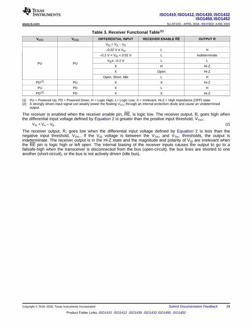
Table 3. Receiver Functional Table (1)
VCC1 VCC2 DIFFERENTIAL INPUT RECEIVER ENABLE RE OUTPUT RVID = VA – VB
PU PU
–0.02 V ≤ VID L H–0.2 V < VID < 0.02 V L Indeterminate
VID≤ –0.2 V L LX H Hi-ZX Open Hi-Z
Open, Short, Idle L HPD (2) PU X X Hi-ZPU PD X L H
PD (2) PD X X Hi-Z
The receiver is enabled when the receiver enable pin, RE, is logic low. The receiver output, R, goes high whenthe differential input voltage defined by Equation 2 is greater than the positive input threshold, VTH+.
VID = VA – VB (2)
The receiver output, R, goes low when the differential input voltage defined by Equation 2 is less than thenegative input threshold, VTH–. If the VID voltage is between the VTH+ and VTH– thresholds, the output isindeterminate. The receiver output is in the Hi-Z state and the magnitude and polarity of VID are irrelevant whenthe RE pin is logic high or left open. The internal biasing of the receiver inputs causes the output to go to afailsafe-high when the transceiver is disconnected from the bus (open-circuit), the bus lines are shorted to oneanother (short-circuit), or the bus is not actively driven (idle bus).
R Output
D and RE Inputs
Input
VCC1 VCC1 VCC1 VCC1
985
1.5 M
DE Input
Input
VCC1 VCC1 VCC1
1.5 M
985
VCC1
R
~20
30
ISO1410, ISO1412, ISO1430, ISO1432ISO1450, ISO1452SLLSF22G –APRIL 2018–REVISED JUNE 2020 www.ti.com
Product Folder Links: ISO1410 ISO1412 ISO1430 ISO1432 ISO1450 ISO1452
Submit Documentation Feedback Copyright © 2018–2020, Texas Instruments Incorporated
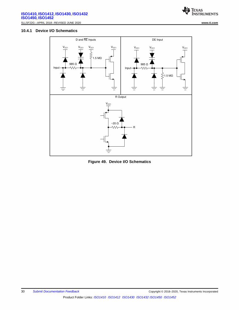
10.4.1 Device I/O Schematics
Figure 49. Device I/O Schematics
Y
Z
A
B
B
A
Z
Y
Z YBA
R
RE
DE D
ISO
14
12
Sla
ve
ISO1412
Master
c
ISO1412
Slave
R
RE
DE
D
R
RE
DE
D
RT
RT
RT
RT
31
ISO1410, ISO1412, ISO1430, ISO1432ISO1450, ISO1452
www.ti.com SLLSF22G –APRIL 2018–REVISED JUNE 2020
Product Folder Links: ISO1410 ISO1412 ISO1430 ISO1432 ISO1450 ISO1452
Submit Documentation FeedbackCopyright © 2018–2020, Texas Instruments Incorporated
11 Application and Implementation
NOTEInformation in the following applications sections is not part of the TI componentspecification, and TI does not warrant its accuracy or completeness. TI’s customers areresponsible for determining suitability of components for their purposes. Customers shouldvalidate and test their design implementation to confirm system functionality.
11.1 Application InformationThe ISO14xx devices are designed for bidirectional data transfer on multipoint RS-485 networks. The design ofeach RS-485 node in the network requires an ISO14xx device and an isolated power supply as shown inFigure 52.
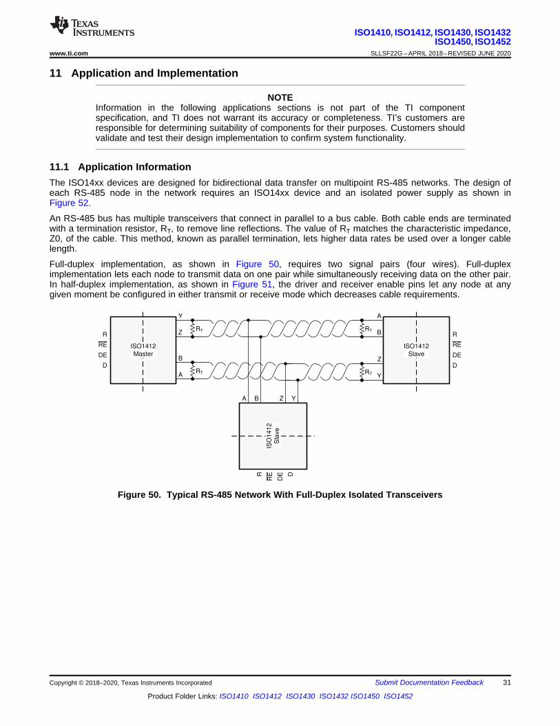
An RS-485 bus has multiple transceivers that connect in parallel to a bus cable. Both cable ends are terminatedwith a termination resistor, RT, to remove line reflections. The value of RT matches the characteristic impedance,Z0, of the cable. This method, known as parallel termination, lets higher data rates be used over a longer cablelength.
Full-duplex implementation, as shown in Figure 50, requires two signal pairs (four wires). Full-dupleximplementation lets each node to transmit data on one pair while simultaneously receiving data on the other pair.In half-duplex implementation, as shown in Figure 51, the driver and receiver enable pins let any node at anygiven moment be configured in either transmit or receive mode which decreases cable requirements.
Figure 50. Typical RS-485 Network With Full-Duplex Isolated Transceivers
PSU
TPS76350
1
2
4
3
5
6
7
8
14
13
12
9,15
IN
EN
GND NC
OUT1
3
5
42
R
VCC1
DE
D
NC
GND1
GND1
RE
NC
B
GND2
4
3
2 6
51
A
NC 10,11
7
8
16VCC2
MCU
GPIO3
GPIO1
VDD
DGND
L1
N
PE
3.3V
0V
Protective
Earth
Chasis
Ground
Digital
Ground
ISO
Ground
Optional bus
protection
Galvanic
Isolation Barrier
ISO1410
SN6505
VCC
D2
D1
GND
CLK
EN3.3 V
GPIO2
0.1 F
A B A B
R
RE
DE
D
A
B
A
B
R
RE
DE D R
RE
DE D
R
RE
DE
D
ISO
14
10
ISO
14
10
Integrated isolation barrier allows for communication between
nodes with ground potential differences of up to 1500 V
ISO1410ISO1410RT RT
32
ISO1410, ISO1412, ISO1430, ISO1432ISO1450, ISO1452SLLSF22G –APRIL 2018–REVISED JUNE 2020 www.ti.com
Product Folder Links: ISO1410 ISO1412 ISO1430 ISO1432 ISO1450 ISO1452
Submit Documentation Feedback Copyright © 2018–2020, Texas Instruments Incorporated
Application Information (continued)
Figure 51. Typical RS-485 Network With Half-Duplex Isolated Transceivers
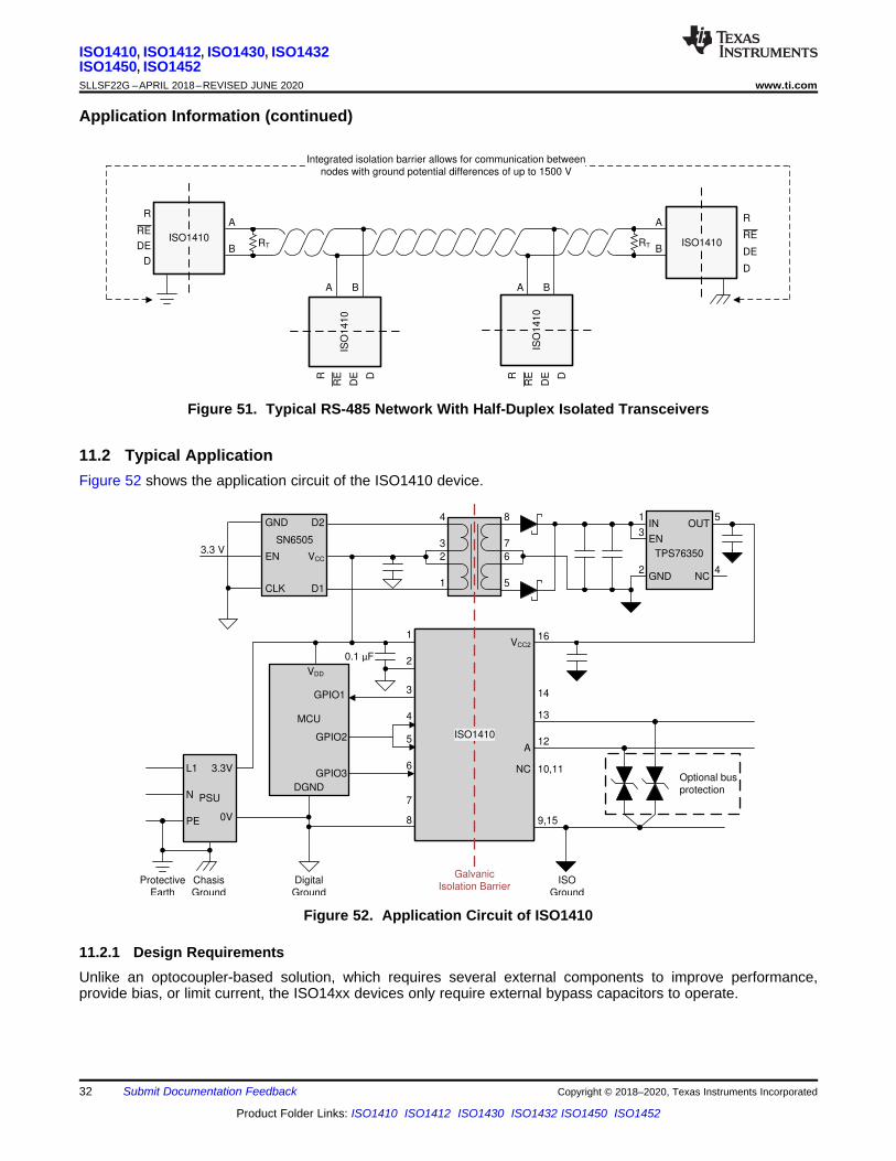
11.2 Typical ApplicationFigure 52 shows the application circuit of the ISO1410 device.
Figure 52. Application Circuit of ISO1410
11.2.1 Design RequirementsUnlike an optocoupler-based solution, which requires several external components to improve performance,provide bias, or limit current, the ISO14xx devices only require external bypass capacitors to operate.

Cable
Length
(ft)
Data Rate (bps)
10000
1000
100
10100 1k 10 k 100 k 1M 10 M 100 M
Conservative
Characteristics
5%, 10%, and 20% Jitter
33
ISO1410, ISO1412, ISO1430, ISO1432ISO1450, ISO1452
www.ti.com SLLSF22G –APRIL 2018–REVISED JUNE 2020
Product Folder Links: ISO1410 ISO1412 ISO1430 ISO1432 ISO1450 ISO1452
Submit Documentation FeedbackCopyright © 2018–2020, Texas Instruments Incorporated
Typical Application (continued)11.2.2 Detailed Design ProcedureThe RS-485 bus is a robust electrical interface suitable for long-distance communications. The RS-485 interfacecan be used in a wide range of applications with varying requirements of distance of communication, data rate,and number of nodes.
11.2.2.1 Data Rate and Bus LengthThe RS-485 standard has typical curves similar to those shown in Figure 53. These curves show the inverserelationship between signaling rate and cable length. If the data rate of the payload between two nodes is lower,the cable length between the nodes can be longer.
Figure 53. Cable Length vs Data Rate Characteristics
Use Figure 53 as a guideline for cable selection, data rate, cable length and subsequent jitter budgeting.
11.2.2.2 Stub LengthIn an RS-485 network, the distance between the transceiver inputs and the cable trunk is known as the stub. Thestub should be as short as possible when a node is connected to the bus. Stubs are a non-terminated piece ofbus line that can introduce reflections of varying phase as the length of the stub increases. The electrical length,or round-trip delay, of a stub should be less than one-tenth of the rise time of the driver as a general guideline.Therefore, the maximum physical stub length (L(STUB)) is calculated as shown in Equation 3.
L(STUB) ≤ 0.1 × tr × v × c
where• tr is the 10/90 rise time of the driver.• c is the speed of light (3 × 10⁸ m/s).• v is the signal velocity of the cable or trace as a factor of c. (3)
11.2.2.3 Bus LoadingThe current supplied by the driver must supply into a load because the output of the driver depends on thiscurrent. Add transceivers to the bus to increase the total bus loading. The RS-485 standard specifies ahypothetical term of a unit load (UL) to estimate the maximum number of possible bus loads. The UL representsa load impedance of approximately 12 kΩ. Standard-compliant drivers must be able to drive 32 of these ULs.
The ISO14xx devices have 1/8 UL impedance transceiver and can connect up to 256 nodes to the bus.
11.2.3 Application CurvesBelow eye diagram of ISO145x device indicates low jitter and wide open eye at maximum data rate of 50 Mbps.
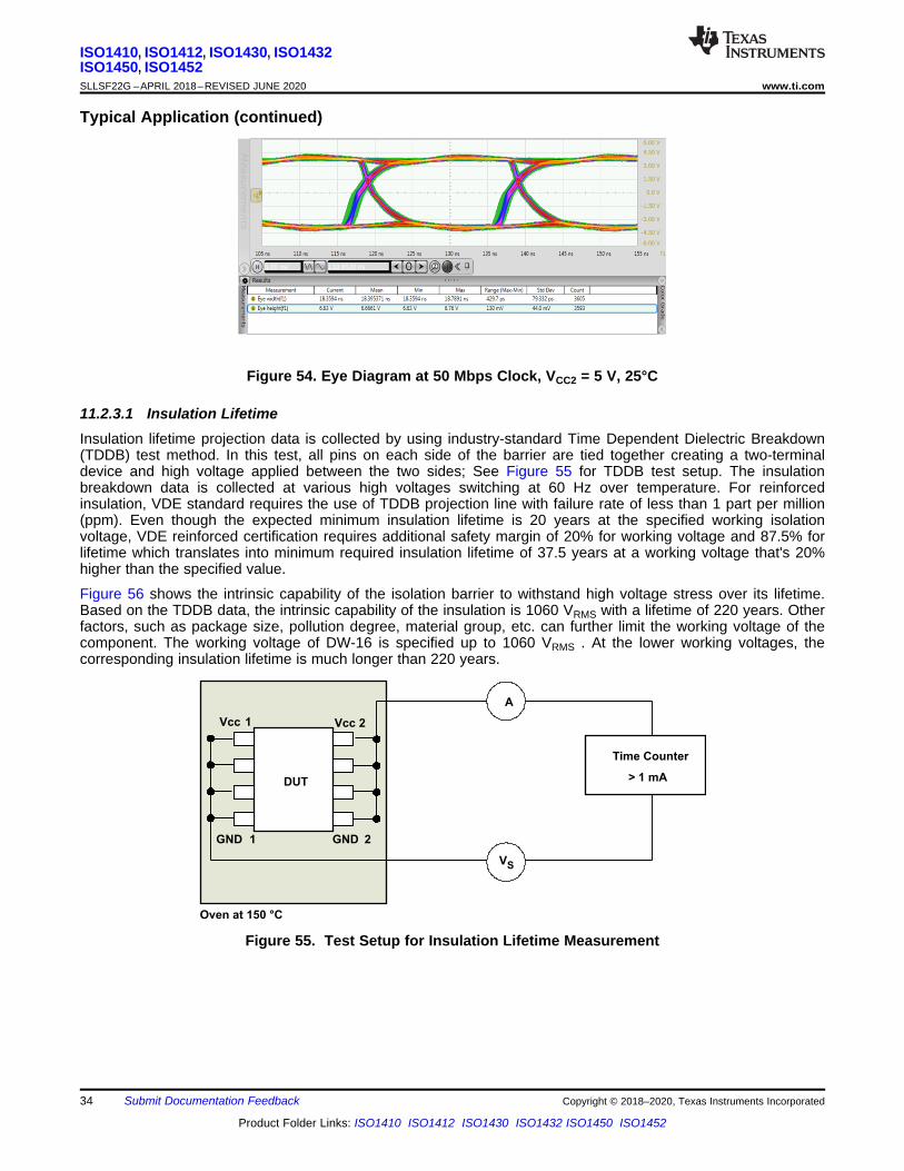
DUT
Vcc 2Vcc 1
GND 1 GND 2
A
Oven at 150 °C
Time Counter
> 1 mA
VS
34
ISO1410, ISO1412, ISO1430, ISO1432ISO1450, ISO1452SLLSF22G –APRIL 2018–REVISED JUNE 2020 www.ti.com
Product Folder Links: ISO1410 ISO1412 ISO1430 ISO1432 ISO1450 ISO1452
Submit Documentation Feedback Copyright © 2018–2020, Texas Instruments Incorporated
Typical Application (continued)
Figure 54. Eye Diagram at 50 Mbps Clock, VCC2 = 5 V, 25°C
11.2.3.1 Insulation LifetimeInsulation lifetime projection data is collected by using industry-standard Time Dependent Dielectric Breakdown(TDDB) test method. In this test, all pins on each side of the barrier are tied together creating a two-terminaldevice and high voltage applied between the two sides; See Figure 55 for TDDB test setup. The insulationbreakdown data is collected at various high voltages switching at 60 Hz over temperature. For reinforcedinsulation, VDE standard requires the use of TDDB projection line with failure rate of less than 1 part per million(ppm). Even though the expected minimum insulation lifetime is 20 years at the specified working isolationvoltage, VDE reinforced certification requires additional safety margin of 20% for working voltage and 87.5% forlifetime which translates into minimum required insulation lifetime of 37.5 years at a working voltage that's 20%higher than the specified value.
Figure 56 shows the intrinsic capability of the isolation barrier to withstand high voltage stress over its lifetime.Based on the TDDB data, the intrinsic capability of the insulation is 1060 VRMS with a lifetime of 220 years. Otherfactors, such as package size, pollution degree, material group, etc. can further limit the working voltage of thecomponent. The working voltage of DW-16 is specified up to 1060 VRMS . At the lower working voltages, thecorresponding insulation lifetime is much longer than 220 years.
Figure 55. Test Setup for Insulation Lifetime Measurement
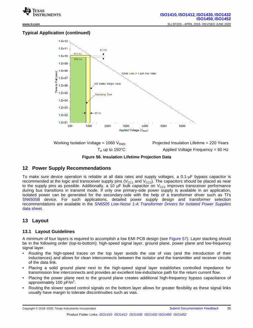
35
ISO1410, ISO1412, ISO1430, ISO1432ISO1450, ISO1452
www.ti.com SLLSF22G –APRIL 2018–REVISED JUNE 2020
Product Folder Links: ISO1410 ISO1412 ISO1430 ISO1432 ISO1450 ISO1452
Submit Documentation FeedbackCopyright © 2018–2020, Texas Instruments Incorporated
Typical Application (continued)
Working Isolation Voltage = 1060 VRMS Projected Insulation Lifetime = 220 YearsTA up to 150°C Applied Voltage Frequency = 60 Hz
Figure 56. Insulation Lifetime Projection Data
12 Power Supply RecommendationsTo make sure device operation is reliable at all data rates and supply voltages, a 0.1-μF bypass capacitor isrecommended at the logic and transceiver supply pins (VCC1 and VCC2). The capacitors should be placed as nearto the supply pins as possible. Additionally, a 10 µF bulk capacitor on VCC2 improves transceiver performanceduring bus transitions in transmit mode. If only one primary-side power supply is available in an application,isolated power can be generated for the secondary-side with the help of a transformer driver such as TI'sSN6505B device. For such applications, detailed power supply design and transformer selectionrecommendations are available in the SN6505 Low-Noise 1-A Transformer Drivers for Isolated Power Suppliesdata sheet.
13 Layout
13.1 Layout GuidelinesA minimum of four layers is required to accomplish a low EMI PCB design (see Figure 57). Layer stacking shouldbe in the following order (top-to-bottom): high-speed signal layer, ground plane, power plane and low-frequencysignal layer.• Routing the high-speed traces on the top layer avoids the use of vias (and the introduction of their
inductances) and allows for clean interconnects between the isolator and the transmitter and receiver circuitsof the data link.
• Placing a solid ground plane next to the high-speed signal layer establishes controlled impedance fortransmission line interconnects and provides an excellent low-inductance path for the return current flow.
• Placing the power plane next to the ground plane creates additional high-frequency bypass capacitance ofapproximately 100 pF/in2.
• Routing the slower speed control signals on the bottom layer allows for greater flexibility as these signal linksusually have margin to tolerate discontinuities such as vias.

Minimize distance to supply pins
x
Iso
latio
n C
ap
acito
r
D1
VCC1 VCC2
RS-485 R
VCC1
GND1
R
RE
DE
D
NC
GND1
Optional bus protection
VCC2
GND2
NC
B
A
NC
NC
GND2
0.1 µF C0.1 µF
GND2Plane
MCU
GND1Plane
C
10 mils
10 mils
40 milsFR-4
0r ~ 4.5
Keep this space
free from planes,
traces, pads, and
vias
Ground plane
Power plane
Low-speed traces
High-speed traces
36
ISO1410, ISO1412, ISO1430, ISO1432ISO1450, ISO1452SLLSF22G –APRIL 2018–REVISED JUNE 2020 www.ti.com
Product Folder Links: ISO1410 ISO1412 ISO1430 ISO1432 ISO1450 ISO1452
Submit Documentation Feedback Copyright © 2018–2020, Texas Instruments Incorporated
Layout Guidelines (continued)Figure 58 shows the recommended placement and routing of the device bypass capacitors and optional TVSdiodes. Put the VCC2 bypass capacitors on the top layer and as near to the device pins as possible. Do not usevias to complete the connection to the VCC2 and GND2 pins. If an additional supply voltage plane or signal layeris needed, add a second power or ground plane system to the stack to keep it symmetrical. This makes the stackmechanically stable and prevents it from warping. Also the power and ground plane of each power system canbe placed closer together, thus increasing the high-frequency bypass capacitance significantly.
Refer to the Digital Isolator Design Guide for detailed layout recommendations.
13.1.1 PCB MaterialFor digital circuit boards operating at less than 150 Mbps, (or rise and fall times greater than 1 ns), and tracelengths of up to 10 inches, use standard FR-4 UL94V-0 printed circuit board. This PCB is preferred over cheaperalternatives because of lower dielectric losses at high frequencies, less moisture absorption, greater strength andstiffness, and the self-extinguishing flammability-characteristics.
13.2 Layout Example
Figure 57. Recommended Layer Stack
Figure 58. Layout Example

37
ISO1410, ISO1412, ISO1430, ISO1432ISO1450, ISO1452
www.ti.com SLLSF22G –APRIL 2018–REVISED JUNE 2020
Product Folder Links: ISO1410 ISO1412 ISO1430 ISO1432 ISO1450 ISO1452
Submit Documentation FeedbackCopyright © 2018–2020, Texas Instruments Incorporated
14 Device and Documentation Support
14.1 Documentation Support
14.1.1 Related DocumentationFor related documentation see the following:• Texas Instruments, Digital Isolator Design Guide• Texas Instruments, Isolation Glossary• Texas Instruments, Isolated RS-485 Half-Duplex Evaluation Module user's guide• Texas Instruments, How to isolate signal and power for an RS-485 system TI TechNote• Texas Instruments, Robust Isolated RS-485 for industrial long-haul communications TI TechNote
14.2 Related LinksThe table below lists quick access links. Categories include technical documents, support and communityresources, tools and software, and quick access to order now.
Table 4. Related Links
PARTS PRODUCT FOLDER ORDER NOW TECHNICALDOCUMENTS
TOOLS &SOFTWARE
SUPPORT &COMMUNITY
ISO1410 Click here Click here Click here Click here Click hereISO1412 Click here Click here Click here Click here Click hereISO1430 Click here Click here Click here Click here Click hereISO1432 Click here Click here Click here Click here Click hereISO1450 Click here Click here Click here Click here Click hereISO1452 Click here Click here Click here Click here Click here
ISO1410B Click here Click here Click here Click here Click hereISO1412B Click here Click here Click here Click here Click hereISO1430B Click here Click here Click here Click here Click hereISO1432B Click here Click here Click here Click here Click hereISO1450B Click here Click here Click here Click here Click hereISO1452B Click here Click here Click here Click here Click here
14.3 Receiving Notification of Documentation UpdatesTo receive notification of documentation updates, navigate to the device product folder on ti.com. In the upperright corner, click on Alert me to register and receive a weekly digest of any product information that haschanged. For change details, review the revision history included in any revised document.
14.4 Community ResourceTI E2E™ support forums are an engineer's go-to source for fast, verified answers and design help — straightfrom the experts. Search existing answers or ask your own question to get the quick design help you need.
Linked content is provided "AS IS" by the respective contributors. They do not constitute TI specifications and donot necessarily reflect TI's views; see TI's Terms of Use.
14.5 TrademarksE2E is a trademark of Texas Instruments.All other trademarks are the property of their respective owners.
14.6 Electrostatic Discharge CautionThis integrated circuit can be damaged by ESD. Texas Instruments recommends that all integrated circuits be handled withappropriate precautions. Failure to observe proper handling and installation procedures can cause damage.
ESD damage can range from subtle performance degradation to complete device failure. Precision integrated circuits may be moresusceptible to damage because very small parametric changes could cause the device not to meet its published specifications.
38
ISO1410, ISO1412, ISO1430, ISO1432ISO1450, ISO1452SLLSF22G –APRIL 2018–REVISED JUNE 2020 www.ti.com
Product Folder Links: ISO1410 ISO1412 ISO1430 ISO1432 ISO1450 ISO1452
Submit Documentation Feedback Copyright © 2018–2020, Texas Instruments Incorporated
14.7 GlossarySLYZ022 — TI Glossary.
This glossary lists and explains terms, acronyms, and definitions.
15 Mechanical, Packaging, and Orderable InformationThe following pages include mechanical packaging and orderable information. This information is the mostcurrent data available for the designated devices. This data is subject to change without notice and revision ofthis document. For browser-based versions of this data sheet, refer to the left-hand navigation.

PACKAGE OPTION ADDENDUM
www.ti.com 28-Sep-2021
Addendum-Page 1
PACKAGING INFORMATION
Orderable Device Status(1)
Package Type PackageDrawing
Pins PackageQty
Eco Plan(2)
Lead finish/Ball material
(6)
MSL Peak Temp(3)
Op Temp (°C) Device Marking(4/5)
Samples
ISO1410BDW ACTIVE SOIC DW 16 40 RoHS & Green NIPDAU Level-2-260C-1 YEAR -40 to 125 ISO1410B
ISO1410BDWR ACTIVE SOIC DW 16 2000 RoHS & Green NIPDAU Level-2-260C-1 YEAR -40 to 125 ISO1410B
ISO1410DW ACTIVE SOIC DW 16 40 RoHS & Green NIPDAU Level-2-260C-1 YEAR -40 to 125 ISO1410
ISO1410DWR ACTIVE SOIC DW 16 2000 RoHS & Green NIPDAU Level-2-260C-1 YEAR -40 to 125 ISO1410
ISO1412BDW ACTIVE SOIC DW 16 40 RoHS & Green NIPDAU Level-2-260C-1 YEAR -40 to 125 ISO1412B
ISO1412BDWR ACTIVE SOIC DW 16 2000 RoHS & Green NIPDAU Level-2-260C-1 YEAR -40 to 125 ISO1412B
ISO1412DW ACTIVE SOIC DW 16 40 RoHS & Green NIPDAU Level-2-260C-1 YEAR -40 to 125 ISO1412
ISO1412DWR ACTIVE SOIC DW 16 2000 RoHS & Green NIPDAU Level-2-260C-1 YEAR -40 to 125 ISO1412
ISO1430BDW ACTIVE SOIC DW 16 40 RoHS & Green NIPDAU Level-2-260C-1 YEAR -40 to 125 ISO1430B
ISO1430BDWR ACTIVE SOIC DW 16 2000 RoHS & Green NIPDAU Level-2-260C-1 YEAR -40 to 125 ISO1430B
ISO1430DW ACTIVE SOIC DW 16 40 RoHS & Green NIPDAU Level-2-260C-1 YEAR -40 to 125 ISO1430
ISO1430DWR ACTIVE SOIC DW 16 2000 RoHS & Green NIPDAU Level-2-260C-1 YEAR -40 to 125 ISO1430
ISO1432BDW ACTIVE SOIC DW 16 40 RoHS & Green NIPDAU Level-2-260C-1 YEAR -40 to 125 ISO1432B
ISO1432BDWR ACTIVE SOIC DW 16 2000 RoHS & Green NIPDAU Level-2-260C-1 YEAR -40 to 125 ISO1432B
ISO1432DW ACTIVE SOIC DW 16 40 RoHS & Green NIPDAU Level-2-260C-1 YEAR -40 to 125 ISO1432
ISO1432DWR ACTIVE SOIC DW 16 2000 RoHS & Green NIPDAU Level-2-260C-1 YEAR -40 to 125 ISO1432
ISO1450BDW ACTIVE SOIC DW 16 40 RoHS & Green NIPDAU Level-2-260C-1 YEAR -40 to 125 ISO1450B
ISO1450BDWR ACTIVE SOIC DW 16 2000 RoHS & Green NIPDAU Level-2-260C-1 YEAR -40 to 125 ISO1450B
ISO1450DW ACTIVE SOIC DW 16 40 RoHS & Green NIPDAU Level-2-260C-1 YEAR -40 to 125 ISO1450
ISO1450DWR ACTIVE SOIC DW 16 2000 RoHS & Green NIPDAU Level-2-260C-1 YEAR -40 to 125 ISO1450
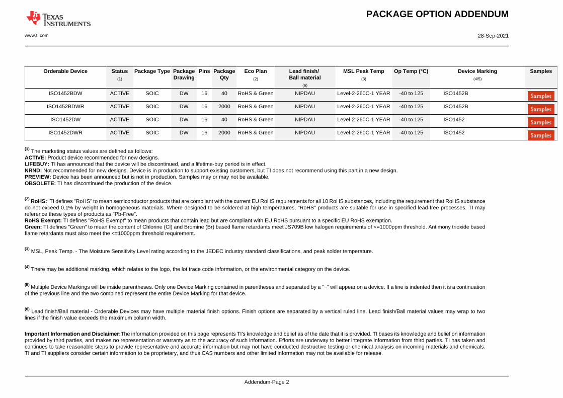
PACKAGE OPTION ADDENDUM
www.ti.com 28-Sep-2021
Addendum-Page 2
Orderable Device Status(1)
Package Type PackageDrawing
Pins PackageQty
Eco Plan(2)
Lead finish/Ball material
(6)
MSL Peak Temp(3)
Op Temp (°C) Device Marking(4/5)
Samples
ISO1452BDW ACTIVE SOIC DW 16 40 RoHS & Green NIPDAU Level-2-260C-1 YEAR -40 to 125 ISO1452B
ISO1452BDWR ACTIVE SOIC DW 16 2000 RoHS & Green NIPDAU Level-2-260C-1 YEAR -40 to 125 ISO1452B
ISO1452DW ACTIVE SOIC DW 16 40 RoHS & Green NIPDAU Level-2-260C-1 YEAR -40 to 125 ISO1452
ISO1452DWR ACTIVE SOIC DW 16 2000 RoHS & Green NIPDAU Level-2-260C-1 YEAR -40 to 125 ISO1452
(1) The marketing status values are defined as follows:ACTIVE: Product device recommended for new designs.LIFEBUY: TI has announced that the device will be discontinued, and a lifetime-buy period is in effect.NRND: Not recommended for new designs. Device is in production to support existing customers, but TI does not recommend using this part in a new design.PREVIEW: Device has been announced but is not in production. Samples may or may not be available.OBSOLETE: TI has discontinued the production of the device.
(2) RoHS: TI defines "RoHS" to mean semiconductor products that are compliant with the current EU RoHS requirements for all 10 RoHS substances, including the requirement that RoHS substancedo not exceed 0.1% by weight in homogeneous materials. Where designed to be soldered at high temperatures, "RoHS" products are suitable for use in specified lead-free processes. TI mayreference these types of products as "Pb-Free".RoHS Exempt: TI defines "RoHS Exempt" to mean products that contain lead but are compliant with EU RoHS pursuant to a specific EU RoHS exemption.Green: TI defines "Green" to mean the content of Chlorine (Cl) and Bromine (Br) based flame retardants meet JS709B low halogen requirements of <=1000ppm threshold. Antimony trioxide basedflame retardants must also meet the <=1000ppm threshold requirement.
(3) MSL, Peak Temp. - The Moisture Sensitivity Level rating according to the JEDEC industry standard classifications, and peak solder temperature.
(4) There may be additional marking, which relates to the logo, the lot trace code information, or the environmental category on the device.
(5) Multiple Device Markings will be inside parentheses. Only one Device Marking contained in parentheses and separated by a "~" will appear on a device. If a line is indented then it is a continuationof the previous line and the two combined represent the entire Device Marking for that device.
(6) Lead finish/Ball material - Orderable Devices may have multiple material finish options. Finish options are separated by a vertical ruled line. Lead finish/Ball material values may wrap to twolines if the finish value exceeds the maximum column width.
Important Information and Disclaimer:The information provided on this page represents TI's knowledge and belief as of the date that it is provided. TI bases its knowledge and belief on informationprovided by third parties, and makes no representation or warranty as to the accuracy of such information. Efforts are underway to better integrate information from third parties. TI has taken andcontinues to take reasonable steps to provide representative and accurate information but may not have conducted destructive testing or chemical analysis on incoming materials and chemicals.TI and TI suppliers consider certain information to be proprietary, and thus CAS numbers and other limited information may not be available for release.

PACKAGE OPTION ADDENDUM
www.ti.com 28-Sep-2021
Addendum-Page 3
In no event shall TI's liability arising out of such information exceed the total purchase price of the TI part(s) at issue in this document sold by TI to Customer on an annual basis.
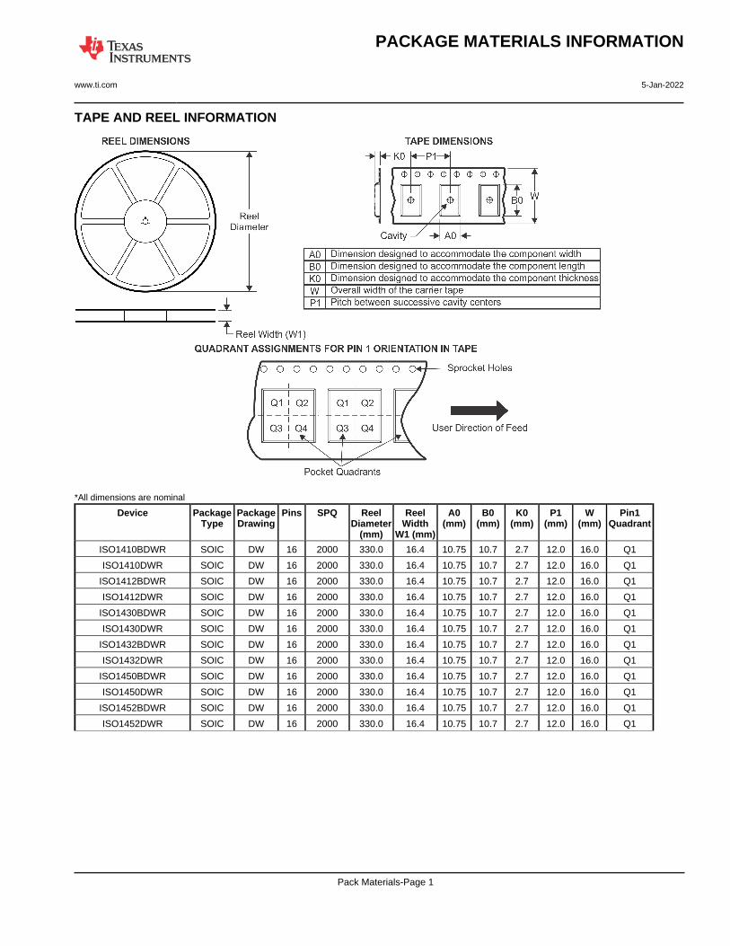
TAPE AND REEL INFORMATION
*All dimensions are nominal
Device PackageType
PackageDrawing
Pins SPQ ReelDiameter
(mm)
ReelWidth
W1 (mm)
A0(mm)
B0(mm)
K0(mm)
P1(mm)
W(mm)
Pin1Quadrant
ISO1410BDWR SOIC DW 16 2000 330.0 16.4 10.75 10.7 2.7 12.0 16.0 Q1
ISO1410DWR SOIC DW 16 2000 330.0 16.4 10.75 10.7 2.7 12.0 16.0 Q1
ISO1412BDWR SOIC DW 16 2000 330.0 16.4 10.75 10.7 2.7 12.0 16.0 Q1
ISO1412DWR SOIC DW 16 2000 330.0 16.4 10.75 10.7 2.7 12.0 16.0 Q1
ISO1430BDWR SOIC DW 16 2000 330.0 16.4 10.75 10.7 2.7 12.0 16.0 Q1
ISO1430DWR SOIC DW 16 2000 330.0 16.4 10.75 10.7 2.7 12.0 16.0 Q1
ISO1432BDWR SOIC DW 16 2000 330.0 16.4 10.75 10.7 2.7 12.0 16.0 Q1
ISO1432DWR SOIC DW 16 2000 330.0 16.4 10.75 10.7 2.7 12.0 16.0 Q1
ISO1450BDWR SOIC DW 16 2000 330.0 16.4 10.75 10.7 2.7 12.0 16.0 Q1
ISO1450DWR SOIC DW 16 2000 330.0 16.4 10.75 10.7 2.7 12.0 16.0 Q1
ISO1452BDWR SOIC DW 16 2000 330.0 16.4 10.75 10.7 2.7 12.0 16.0 Q1
ISO1452DWR SOIC DW 16 2000 330.0 16.4 10.75 10.7 2.7 12.0 16.0 Q1
PACKAGE MATERIALS INFORMATION
www.ti.com 5-Jan-2022
Pack Materials-Page 1
*All dimensions are nominal
Device Package Type Package Drawing Pins SPQ Length (mm) Width (mm) Height (mm)
ISO1410BDWR SOIC DW 16 2000 350.0 350.0 43.0
ISO1410DWR SOIC DW 16 2000 350.0 350.0 43.0
ISO1412BDWR SOIC DW 16 2000 350.0 350.0 43.0
ISO1412DWR SOIC DW 16 2000 350.0 350.0 43.0
ISO1430BDWR SOIC DW 16 2000 350.0 350.0 43.0
ISO1430DWR SOIC DW 16 2000 350.0 350.0 43.0
ISO1432BDWR SOIC DW 16 2000 350.0 350.0 43.0
ISO1432DWR SOIC DW 16 2000 350.0 350.0 43.0
ISO1450BDWR SOIC DW 16 2000 350.0 350.0 43.0
ISO1450DWR SOIC DW 16 2000 350.0 350.0 43.0
ISO1452BDWR SOIC DW 16 2000 350.0 350.0 43.0
ISO1452DWR SOIC DW 16 2000 350.0 350.0 43.0
PACKAGE MATERIALS INFORMATION
www.ti.com 5-Jan-2022
Pack Materials-Page 2

TUBE
*All dimensions are nominal
Device Package Name Package Type Pins SPQ L (mm) W (mm) T (µm) B (mm)
ISO1410BDW DW SOIC 16 40 506.98 12.7 4826 6.6
ISO1410DW DW SOIC 16 40 506.98 12.7 4826 6.6
ISO1412BDW DW SOIC 16 40 506.98 12.7 4826 6.6
ISO1412DW DW SOIC 16 40 506.98 12.7 4826 6.6
ISO1430BDW DW SOIC 16 40 506.98 12.7 4826 6.6
ISO1430DW DW SOIC 16 40 506.98 12.7 4826 6.6
ISO1432BDW DW SOIC 16 40 506.98 12.7 4826 6.6
ISO1432DW DW SOIC 16 40 506.98 12.7 4826 6.6
ISO1450BDW DW SOIC 16 40 506.98 12.7 4826 6.6
ISO1450DW DW SOIC 16 40 506.98 12.7 4826 6.6
ISO1452BDW DW SOIC 16 40 506.98 12.7 4826 6.6
ISO1452DW DW SOIC 16 40 506.98 12.7 4826 6.6
PACKAGE MATERIALS INFORMATION
www.ti.com 5-Jan-2022
Pack Materials-Page 3

www.ti.com
GENERIC PACKAGE VIEW
This image is a representation of the package family, actual package may vary.Refer to the product data sheet for package details.
SOIC - 2.65 mm max heightDW 16SMALL OUTLINE INTEGRATED CIRCUIT7.5 x 10.3, 1.27 mm pitch
4224780/A

www.ti.com
PACKAGE OUTLINE
C
TYP10.639.97
2.65 MAX
14X 1.27
16X 0.510.31
2X8.89
TYP0.330.10
0 - 80.30.1
(1.4)
0.25GAGE PLANE
1.270.40
A
NOTE 3
10.510.1
BNOTE 4
7.67.4
4221009/B 07/2016
SOIC - 2.65 mm max heightDW0016BSOIC
NOTES: 1. All linear dimensions are in millimeters. Dimensions in parenthesis are for reference only. Dimensioning and tolerancing per ASME Y14.5M. 2. This drawing is subject to change without notice. 3. This dimension does not include mold flash, protrusions, or gate burrs. Mold flash, protrusions, or gate burrs shall not exceed 0.15 mm, per side. 4. This dimension does not include interlead flash. Interlead flash shall not exceed 0.25 mm, per side.5. Reference JEDEC registration MS-013.
1 16
0.25 C A B
98
PIN 1 IDAREA
SEATING PLANE
0.1 C
SEE DETAIL A
DETAIL ATYPICAL
SCALE 1.500
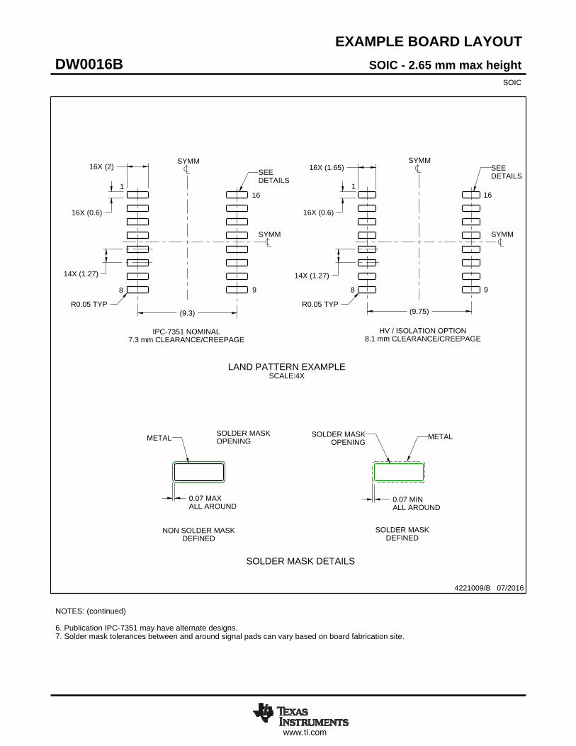
www.ti.com
EXAMPLE BOARD LAYOUT
(9.75)R0.05 TYP
0.07 MAXALL AROUND
0.07 MINALL AROUND
(9.3)
14X (1.27)
R0.05 TYP
16X (1.65)
16X (0.6)
14X (1.27)
16X (2)
16X (0.6)
4221009/B 07/2016
SOIC - 2.65 mm max heightDW0016BSOIC
SYMM
SYMM
SEEDETAILS
1
8 9
16
SYMM
HV / ISOLATION OPTION8.1 mm CLEARANCE/CREEPAGE
NOTES: (continued) 6. Publication IPC-7351 may have alternate designs. 7. Solder mask tolerances between and around signal pads can vary based on board fabrication site.
METAL SOLDER MASKOPENING
NON SOLDER MASKDEFINED
SOLDER MASK DETAILS
OPENINGSOLDER MASK METAL
SOLDER MASKDEFINED
LAND PATTERN EXAMPLESCALE:4X
SYMM
1
8 9
16
IPC-7351 NOMINAL7.3 mm CLEARANCE/CREEPAGE
SEEDETAILS

www.ti.com
EXAMPLE STENCIL DESIGN
R0.05 TYPR0.05 TYP
16X (1.65)
16X (0.6)
14X (1.27)
(9.75)
16X (2)
16X (0.6)
14X (1.27)
(9.3)
4221009/B 07/2016
SOIC - 2.65 mm max heightDW0016BSOIC
NOTES: (continued) 8. Laser cutting apertures with trapezoidal walls and rounded corners may offer better paste release. IPC-7525 may have alternate design recommendations. 9. Board assembly site may have different recommendations for stencil design.
SYMM
SYMM
1
8 9
16
HV / ISOLATION OPTION8.1 mm CLEARANCE/CREEPAGE
SOLDER PASTE EXAMPLEBASED ON 0.125 mm THICK STENCIL
SCALE:4X
SYMM
SYMM
1
8 9
16
IPC-7351 NOMINAL7.3 mm CLEARANCE/CREEPAGE

IMPORTANT NOTICE AND DISCLAIMERTI PROVIDES TECHNICAL AND RELIABILITY DATA (INCLUDING DATA SHEETS), DESIGN RESOURCES (INCLUDING REFERENCE DESIGNS), APPLICATION OR OTHER DESIGN ADVICE, WEB TOOLS, SAFETY INFORMATION, AND OTHER RESOURCES “AS IS” AND WITH ALL FAULTS, AND DISCLAIMS ALL WARRANTIES, EXPRESS AND IMPLIED, INCLUDING WITHOUT LIMITATION ANY IMPLIED WARRANTIES OF MERCHANTABILITY, FITNESS FOR A PARTICULAR PURPOSE OR NON-INFRINGEMENT OF THIRD PARTY INTELLECTUAL PROPERTY RIGHTS.These resources are intended for skilled developers designing with TI products. You are solely responsible for (1) selecting the appropriate TI products for your application, (2) designing, validating and testing your application, and (3) ensuring your application meets applicable standards, and any other safety, security, regulatory or other requirements.These resources are subject to change without notice. TI grants you permission to use these resources only for development of an application that uses the TI products described in the resource. Other reproduction and display of these resources is prohibited. No license is granted to any other TI intellectual property right or to any third party intellectual property right. TI disclaims responsibility for, and you will fully indemnify TI and its representatives against, any claims, damages, costs, losses, and liabilities arising out of your use of these resources.TI’s products are provided subject to TI’s Terms of Sale or other applicable terms available either on ti.com or provided in conjunction with such TI products. TI’s provision of these resources does not expand or otherwise alter TI’s applicable warranties or warranty disclaimers for TI products.TI objects to and rejects any additional or different terms you may have proposed. IMPORTANT NOTICE
Mailing Address: Texas Instruments, Post Office Box 655303, Dallas, Texas 75265Copyright © 2022, Texas Instruments Incorporated