lllllliiilllllllll - fermilab | technical publications
TRANSCRIPT
lllllliiilllllllll o 1160 0093121 b
£t97/J31eV
BENEMERITA UNIVERSIDAD AUTONOMA DE PUEBLA
FACULTAD DE CIENCIAS FISICO MATEMATICAS POSGRADO EN OPTOLECTRONICA
THESIS
"The Development o(Sof{ware to Characterize the Fermilab Pixel Read9ut Chiu for the BTeV experiment"
Submitted in satisfaction of the requirements for the Ph. D. in Physics with Specialty in Optoelectronics
Present
M. C. Maria Aurora Diozcora Vargas Trevino 1 ,.--
Advisor
Dr. Marleigh Sheaff 2
December 2000
f-t-<2-JAILA6--1H E:- s rs-~ OAJ - 1 i
FERM1LAB LIBRARY
1 Scholarship holder from CONACyT, MEXICO/Work developed in a stay at Fermi/ab, Batavia, Ill, USA 2 University of Wisconsin, Madison, USAICINVESTA i~ MEXICO

ACKNOWLEDGEMENTS
I want to thank God for allowing me to be able to meet this enormous challenge in my life.
I want to express my most sincere acknowledgement to my husband Sergio Vergara Limon for all his help in the development of this work and for loving me so much, and to my daughters Teresita and Aurorita for their patience and love.
I want to acknowledge my parents Lie. Marciano Vargas Minor and Lie. Alejandra Concepcion Trevino Lopez, because for their help and love for me.
I whish to thank my advisor Marleigh Sheaff for all her help and advice during the curse of this project.
I whish to thank S. Zimmermann for advice during the course of this project and G. Chiodini for technical assistance. I also want to express my appreciation to the Fermilab staff and management, with special thanks to J. Appel, S. Kwan, and E. Barsotti. This work would not have been possible without the support and encouragement of A. Cordero and A. Fernandez of FCFM/BUAP. The support of the U.S. DOE and CONACyT, Mexico, is also gratefully acknowledged.
TABLE OF CONTENTS
INTRODUCTION
CHAPTER ONE
THE BTeV EXPERIMENT AT FERMILAB
I.I 7'he BTeVexperiment 1.2 Pixel plane 1.3 Requirements for the Vertex Detector
1.-1 Conclusions
CHAPTER TWO
IBE FPIXI CHIP AND THE MULTI CHIP MODULE (MCM)
2.1 The FPIXI chip 2.1. I Fermi/ab Pixel Chip I 2.1.2 Pad description and physical dimensions 2./.3 Scan paths and Readout 2.1.4 Design of patterns to control the FPIXI chip.
Page I 3 5 8
JJage 9 9 15 19 22
,_
2.2 The Multi Chip Module (MCM) 2.2. l High Density Interconnect Circuits (HD!) 2.2.2 Operation of the MCM 2.2.3 Design of patterns to control the MCM
2.3 Conclusions
CHAPTER THREE
CHARACTERIZATION
3.1 Bad pixel map test 3.2 Threshold uniformity and noise tests without and with sensors on it 3.3 Reproducibility 3. 4 Hit studies 3. 5 Test Setup 3.6 Conclusions
CHAPTER FOUR
SOFTWARE
-I.I fhe LabV!EWframework 4.2 Data Acquisition System 4.3 Data Analysis System 4.-1 General Flow Diagram 4. 5 Conclu.~ions
CHAPTER FIVE
RESULTS OF THE CHARACTERIZATION
Page 24 24 25 27 29
Page 31 31 33 33 33 36
Page 38 40 54 60 61
Page 5.1 Bad pixel map 62 5.2 Results of the single FP!Xl chip 63 5.3 Multi C/11p Module (MCM) without sensors, threshold uniformity and noise test 67 5.4 Multi Chip J\1odule (MCM) with sensors, threshold uniformity and noise test 81 5.5 Reproducibility test 82 5.6 Hit studies 84 5. 7 Other test developed on the MCM 85 5.8 Characterizing lhe MCM wilh its readout and control interface 90
5.9 Conclusions
GENERAL CONCLUSIONS
REFERENCES
APENDIXA SCHEMA TIC OF THE SINGLE FPIXl BOARD
APENDIXB SCHEMATIC OF THE MULTI CHIP MODULE (MCM)
Page 92
93
96
INTRODUCTION
High-energy physics is the science of the fundamental nature of matter. Studying subatomic particles and forces gives us a key to understanding the simple physical laws that govern the universe. In 1965, the United States Joint Committee on Atomic Energy (JCAE) and the National Academy of Sciences (NAS) approved a frontier high energy physics project to develop a 200 GeV Accelerator. In 1967, Robert R. Wilson was chosen by URA (Universities Research Association, Inc) as the first Director of the National Accelerator Laboratory (NAL). In 1974, the Laboratory was renamed in honor of Enrico Fenni as Fenni National Accelerator Laboratory. Physicists use accelerators of higher and higher energies to probe deeper and deeper inside the nucleus. Like a more powerful microscope, the higher and higher energy accelerators enable the investigation of smaller and smaller distances, by now even distances inside the proton. Higher energy accelerators also enable the production of heavier and rarer particles.
The search for new particles using the Fennilab accelerator produced a discovery in 1977, the first evidence for the bottom quark. Later on the first superconducting accelerator was constructed in the same tunnel as the original one, called the main ring. This new accelerator was later transfonned into a proton-antiproton collider. The beam of particles begins as negative hydrogen ions in the Cockcroft-Walton accelerator. They continue to the Linac (Linear accelerator). As the beam of negative hydrogen ions enters the third accelerator, the circular Booster, both electrons are stripped off leaving a proton beam. Finally the protons are injected into the Main Ring. The antiproton source was essential to produce the proton's opposite particle. These antiprotons could then be steered into collision with protons and observed in specially designed detectors. The energy of these collisions would be close to 2 TeV in the center of mass. In 1985 the beam reached 800 Ge V, and the first collisions of protons and anti protons (combined energy of 1.6 TeV) were observed at the Colliding Detector at Fennilab (CDF). With the highest energy yet achieved the most powerful superconducting accelerator in the world the began the search for the most exotic particle within reach: the top quark Two specialized detectors were constructed by large teams of experimenters at CDF and at DZero. In 1995 both the CDF and Dzero teams announced the top's discovery.
Under the command of John Peoples until 1999 and now under Michel Witherell the most powerful particle accelerator on earth, Fennilab's Tevatron, gives scientists from all over the United States and the world the opportunity to work together on experiments to try to understand the laws of nature. The Tevatron accelerates protons and antiprotons in a giant underground ring. When proton and antiproton collide at close to the speed of light, they make a tiny fireball of pure energy as intense as the big bang, when the universe was a trillionth of a
second old. Some of the energy turns into matter, according to Einstein's famous equation, E = mC 2
, yielding sprays of particles that may hold answers to our questions about the laws and origin of the universe.
As the program at Fermilab moves forward the particle physics field focuses inside the quark and beyond. Fixed-target and colliding-beams experiments continue their searches on the frontier. In order to contribute to a deeper understanding of the heavy quarks, bottom and top. Fermilab has approved the BTeV experiment, E897. The new Fermilab's Tevatron will produce more than 400 billion b-flavored hadrons per year and IO times as many c-flavored hadrons per year. A hadron is a particle made of strongly-interacting constituents (quarks and/or gluons). These include the mesons and baryons. Such particles participate in residual strong interactions. The heavy-flavored band a hadrons will be an excellent resource with which to investigate CP violation, quark/anti-quark mixing and rare decays. BTeV will be well positioned to answer the most crucial questions in heavy flavor physics. BTeV will use a powerful magnet, called SM3, which already exists at Fermilab. The other important parts of the experiment include the vertex detector, the RICH detectors, the EM calorimeters, and the muon system.
The pixel detector is a multi-plane pixel device that will sit inside the beam pipe. This silicon pixel detector has been proposed to be used in the first level trigger of the BTeV experiment. Thus, the BTe V pixel detector is central to the capability of the BTe V experiment. The major components for the pixel detector system will be the sensor, readout chip, sensor-toreadout-chip connection, mechanical support and cooling, high-density interconnection between the readout chips and the control chips on the detector plane peripheries, and the multiplexing and data transmission to the first-level trigger.
The silicon pixel detector will be composed of 62 pixel planes of IOOx lOOmm each, divided into 31 stations with two planes each, placed perpendicular to the colliding beam and installed a few millimeters from the beam. VLSI pixel readout chips containing front-end electronics for every pixel sensor will be bump-bonded to the detector. Since this detector will be employed for on-line track finding for the lowest level trigger system, the pixel chip will have to read out all detected hits. The pixel chip development involves a succession of steps and submissions toward a chip that meets the BTeV requirements. VLSI chips with pixel unit cells of the same dimensions have been designed and built to instrument the sensors. The chips resulting from these steps have been dubbed FPIXO, FPIXI, and so on. The FPIXl represents the first step towards the final pixel readout architecture. The FPIX l chip is a column-based pixel chip with SO µm x 400 µm pixel cells arranged in an array of 160 rows by l 8 columns for a total of 2880 pixel cells. Current FPIXI prototypes have sensitive areas of up to 59.2 mm2
. In order to gain experience on the technical issues Fermilab has made a five-readout-chip sub-assembly with flexible cable interconnections, called the Fermilab multi chip module, or MCM.
Since each FPIX l chip contains 2880 channels, and the experiment will use about 13000 chips, the task of characterizing them is challenging and potentially time consuming. We developed software within the Lab VIEW framework to control a set of instruments to perform bad pixel map, threshold and noise tests on a full chip in a few hours of running. We also developed software to characterize the Fennilab Pixel module. My thesis work was performed as part of the research and development needed in order to build the pixel detector.
The main goal of the thesis is:
"To develop a test stand including the test setup and software to characterize the Fermi/ab Pixel Readout chip (FPIXJ) for the BTeV experiment"
In order to research the main goal of my thesis, we will describe as an abstract all the chapters containing in my thesis as folJows:
In chapter one we give a brief explanation of the BTe V experiment. First we discuss the requirements of the experiment, explaining its goal. We also include a brief explanation of the parts of the experiment, e.g., the pixel detector.
In chapter two we describe the fPD( I chip and the multi chip module (MCM). We give an extended explanation of how to handle and operate this chip. We give details on how we designed the patterns to control the chip in order to download and readout infonnation from it. We show real photographs of the chip and also for the multi-chip module that contains five FPIXI chips connected in daisy chain. As for the single fPD(I chip we describe the correct way to download to and readout infonnation from the MCM, describing all the signals that allow us to characterize it.
In chapter three we cover in detail the characterization of the FPIXI chip, explaining the different tests that we perfonned on it, including the bad pixel map test, threshold unifonnity test without sensors and with sensors bump-bonded to it, the reproducibility test, hit studies and other studies of interest. Later in this chapter we describe the test setup arranged to carry out all the characterization.
In chapter four we will describe the first test stand used (setup and software) to characterize the fPD(l chips, which took about 157 hours (6.5 days) of running to characterize only one fPD(I chip, which means 786 hours (32 days) of running to characterize 5 FPIXl chips connected in daisy chain. The final version after an optimization of the test setup and software takes only 6 hours of running to characterize an MCM with 5 FPO( I chips connected in daisy chain. And it could be possible decrease the running time injecting more than 17 cells at a time, because the most recently test using a computer with a 750 MHz processor speed shows that the process time is of only about 2 hours of running to characterize a MCM with 5 FPIXI chips connected in daisy chain. Also, we show the development of the software used in the last version of the test stand. The software developed utilizes the Lab VIEW (Laboratory Virtual Instrument Engineering Workbench) framework. LabVIEW is a development environment based on the graphical programming language G. It is integrated fully for communication with hardware such as GPIB, VXI, PXI, RS-232, RS-485, and plug in data acquisition boards. The software is a very important part of the tests, because it is by means of the software that we can control all the phases in the test. We describe the data acquisition system and the data processing system.
In chapter five we report the results obtained in the tests that we described in chapter three. Finally we give the references show and two appendices. As appendix A we show the layout and pin assignment for the single FPIX 1 chip as mounted on the single-chip test board, and as appendix B, we show the layout and pin assignment of the multi chip module (MCM) assembly.
With the automatic characterization of the MCMs we are contributing to develop the first prototype of the half pixel plane for the BTeV Pixel Detector.
With this work we did the follow presentations and publications
Presentations:
1. M.A. Vargas, M. Sheaff, S. Vergara, "The development of software to characterize the fermilab pixel readout chip for the BTeV experiment", Poster presentation, SOMI XIV CONGRESO DE INSTRUMENTACION, Tonanzintla, Puebla, MEXICO 1999.
2. S. Zimmermann, S. Kwan, G. Cancelo, G. Cardoso, S. Cihangir, D. Christian, R. Downing, M. A Vargas, et al., "Development of high data readout rate pixel module and detector hybridization at Fermilab", Poster presentation, PIXEL 2000, Genoa, June 2000.
3. G. Cancelo, S. Vergara, M.A. Vargas, et al., "Fiber optic based readout for the BteV's pixel detector", Poster presentation, LEB Sixth workshop on electronics for the LHC experiment, Cracow, Poland, September 2000.
Publications:
1. M.A. Vargas, M. Sheaff, S. Vergara, "The development of software to characterize the fermilab pixel readout chip for the BTeV experiment", Preceedings of the SOMI XIV CONGRESO DE INSTRUMENT ACION, pp. 608-612, Tonanzintla, Puebla, MEXICO 1999.
2. M.A. Vargas, M. Sheaff, S. Vergara, "The development of software to characterize the Fermilab pixel readout chip, FPIXl, for the BTeV experiment", Accepted to NIMA, November 2000. Fermilab preprint FERMILAB-PUB-00-244E, November 2000.
3. S. Zimmermann, S. Kwan, G. Cancelo, G. Cardoso, S. Cihangir, D. Christian, R. Downing, M. A. Vargas, et al., "Development of high data readout rate pixel module and detector hybridization at Fermilab", Preceedings of the PIXEL 2000, Genoa, June 2000.
4. G. Cancelo, S. Vergara, M.A. Vargas, et al., "Fiber optic based readout for the BteV's pixel detector", Preceedings of the LEB Sixth workshop on electronics for the LHC experiment, Cracow, Poland, October 2000.
CHAPTER ONE
THE BTeV EXPERIMENT AT FERMILAB
The subject of the BTeV experiment is to learn more about the bottom and charm quarks. The experiment will use the Fermilab Tevatron. The accelerator will produce more than 400 billion b-flavored hadrons per year and 10 times as many c-flavored hadrons per year. These particles participate in residual strong interactions. The heavy flavored hadrons will be an excellent resource with which to investigate CP violation, quark/anti-quark mixing and rare decays. With all the results expected from the experiment, BTeV will be well positioned to answer the most crucial questions in heavy flavor physics.
1.1 THE BTeV EXPERIMENT
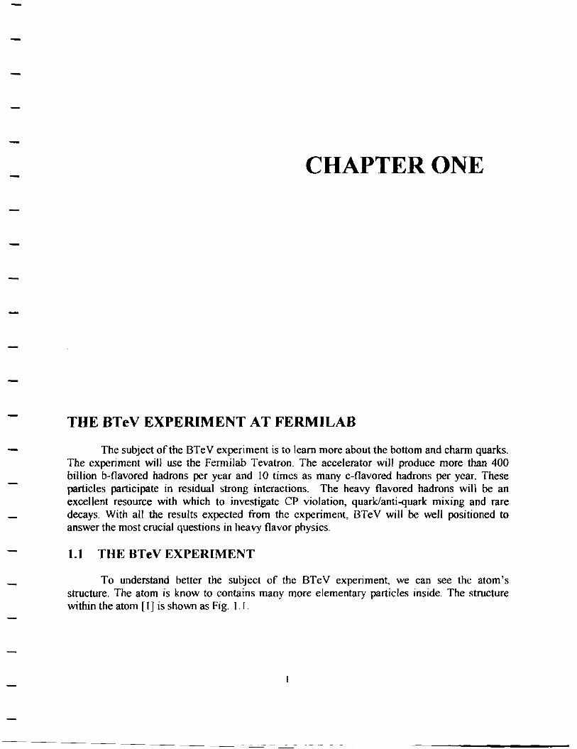
To understand better the subject of the BTeV experiment, we can see the atom's structure. The atom is know to contains many more elementary particles inside. The structure within the atom [I] is shown as Fig. 1. 1 .
.__Atom -10
Size= 10 m
Jfd..1...-.. ........ u.ddsptwa -..u 11 Clll .... .., ._the ....... ......... _Ui .. ._ d.at.l -
la dze ..a 61! en&. atnn-.wlille ..... 11 .... --.i
Figure 1.1: The structure within the atom (this picture is a conception of an artist in a work made/or Fermi/ab).
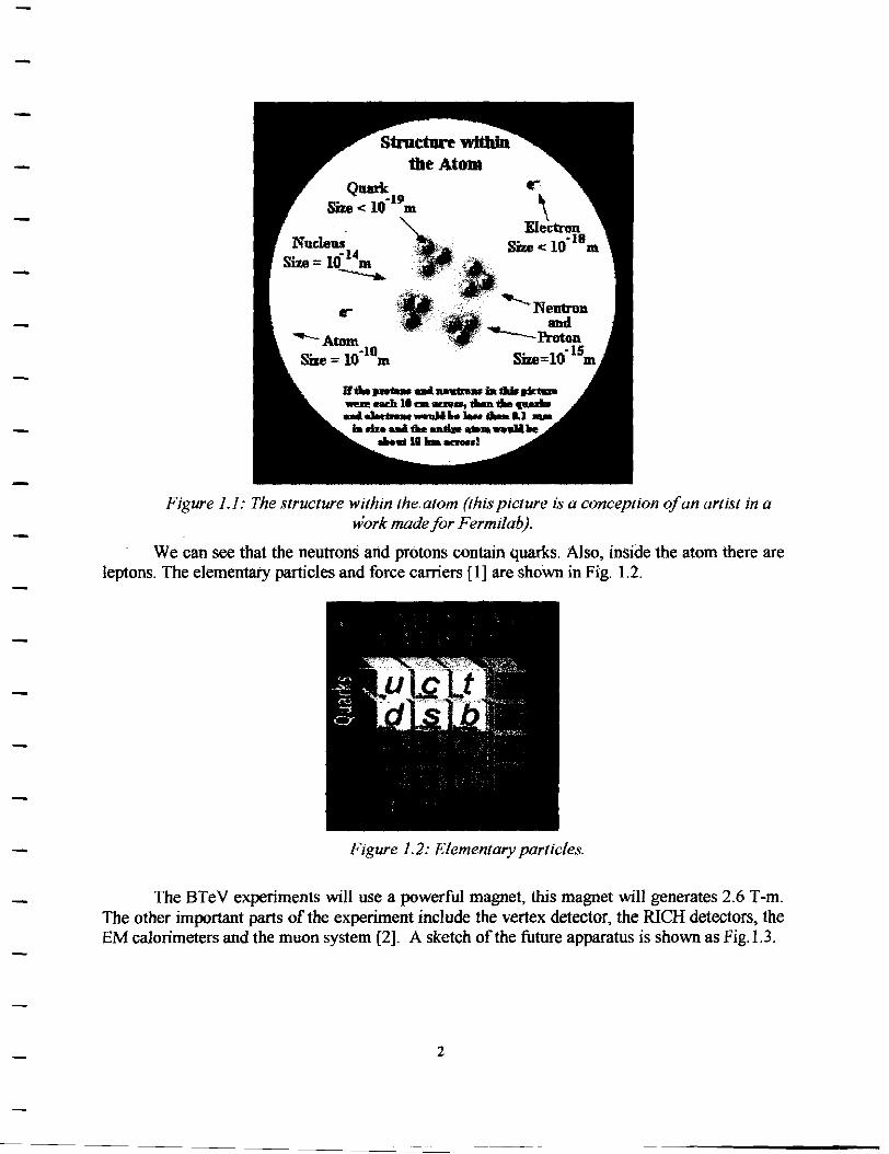
We can see that the neutrons and protons contain quarks. Also, inside the atom there are leptons. The elementary particles and force carriers ( 1] are sho\vn in Fig. 1.2.
Figure 1.2: Elementary particles.
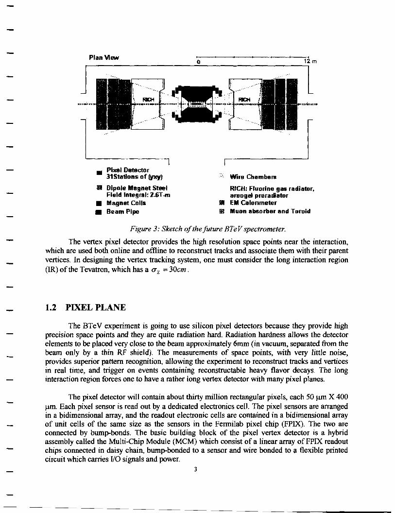
The BTeV experiments will use a powerful magnet, this magnet will generates 2.6 T-m. The other important parts of the experiment include the vertex detector, the RICH detectors, the EM calorimeters and the muon system (2]. A sketch of the future apparatus is shown as Fig.1.3.
2
Plan View 0 12m
J l
• Pixel Detector 31Stetions of (yxy) Wire Chambers
Ii Dipole Magnet Steel RICH: fluorine gas radiator, Field Integral: 2.6T ..m areogeJ preradiator
• Magnet Coils Ill Elll Calonmeter
• Beam Pipe ii Muon absorber and Toroid
Figure 3: Sketch of the future BTeV spectrometer.
The vertex pixel detector provides the high resolution space points near the interactio~ which are used both online and offiine to reconstruct tracks and associate them with their parent vertices. In designing the vertex tracking system, one must consider the long interaction region (IR) of the Tevatron, which has a a z = 30cm.
1.2 PIXEL PLANE
The BTeV experiment is going to use silicon pixel detectors because they provide high precision space points and they are quite radiation hard. Radiation hardness allows the detector elements to be placed very close to the beam approximately 6mm (in vacuum, separated from the beam only by a thin RF shield). The measurements of space points, with very little noise, provides superior pattern recognition, allowing the experiment to reconstruct tracks and vertices in real time, and trigger on events containing reconstructable heavy flavor decays. The long interaction region forces one to have a rather long vertex detector with many pixel planes.
The pixel detector will contain about thirty million rectangular pixels, each 50 µm X 400 µm. Each pixel sensor is read out by a dedicated electronics cell. The pixel sensors are arranged in a bidimensional array, and the readout electronic cells are contained in a bidimensional array of unit cells of the same size as the sensors in the Fermilab pixel chip (FPIX). The two are connected by bump-bonds. The basic building block of the pixel vertex detector is a hybrid assembly called the Multi-Chip Module (MCM) which consist of a linear array of FPIX readout chips connected in daisy chain, bump-bonded to a sensor and wire bonded to a flexible printed circuit which carries I/O signals and power.
3
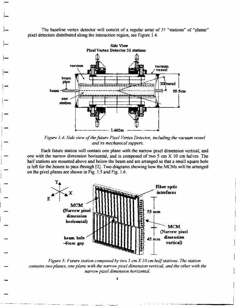
[ The baseline vertex detector will consist of a regular array of 31 "stations" of "planar"
pixel detectors distributed along the interaction region, see Figure 1.4.
beam pipe
one station
Side View Pixel Vertex Detector 31 stations
59.!an
------- l.462m
Figure 1.4: Side view of the future Pixel Vertex Detector, including the vacuum vessel and its mechanical support.
Each future station will contain one plane with the narrow pixel dimension vertical, and one with the narrow dimension horizontal, and is composed of two 5 cm X 10 cm halves. The half stations are mounted above and below the beam and are arranged so that a small square hole is left for the beams to pass through [2]. Two diagrams showing how the MCMs will be arranged on the pixel planes are shown in Fig. 1.5 and Fig. 1.6.
MCM (Narrow pixel
dimension IF1~~LLU horizontal)
beam hole --Omm gap
Fiber optic interfaces
T
Figure 5: Future station composed by two 5 cm X I 0 cm half stations. The station contains two planes, one plane with the narrow pixel dimension vertical, and the other with the
narrow pixel dimension horizontal.
4
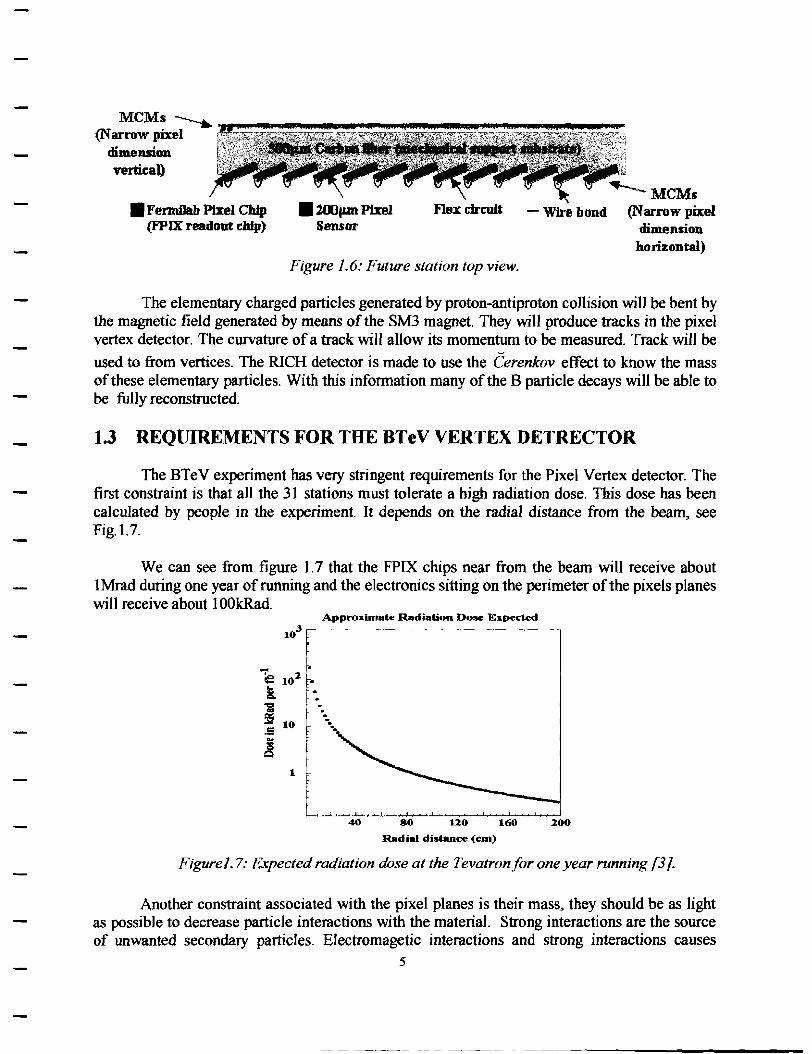
MCMs---...._ (Narrow pixel .... --"""""~""'llllilNl'llll..., __ ....,"""".,..."""'.,.. __ ......,"""'"""'111111111~
dimension vertical)
..__MCMs • FemdJab Ph:el Chip
(FPIX readout chip) • lCllf'ln Pixel
Sensor flex circuit - Wire bond (Narrow pixel
Figure 1.6: Future station top view.
dimension horizontal)
The elementary charged particles generated by proton-antiproton collision will be bent by the magnetic field generated by means of the SM3 magnet. They will produce tracks in the pixel vertex detector. The curvature of a track will allow its momentum to be measured. Track will be
used to from vertices. The RICH detector is made to use the Cerenkov effect to know the mass of these elementary particles. With this information many of the B particle decays will be able to be fully reconstructed.
1.3 REQUIREMENTS FOR THE BTeV VERTEX DETRECTOR
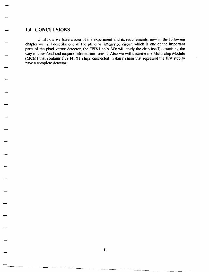
The BTeV experiment has very stringent requirements for the Pixel Vertex detector. The first constraint is that all the 31 stations must tolerate a high radiation dose. This dose has been calculated by people in the experiment. It depends on the radial distance from the beam, see Fig.1.7.
We can see from figure 1.7 that the FPIX chips near from the beam will receive about lMrad during one year of running and the electronics sitting on the perimeter of the pixels planes will receive about 1 OOkRad.
Approximate Radiation Dose Expected
103r-~
- ~ is IO:i •
~
i .s 10
~ 1
40 80 120 160
Radiu distance (cm)
200
Figure/. 7: Expected radiation dose at the Tevatron for one year running [3 /.
Another constraint associated with the pixel planes is their mass, they should be as light as possible to decrease particle interactions with the material. Strong interactions are the source of unwanted secondary particles. Electromagetic interactions and strong interactions causes
5

scattering, which increases the error in the track's reconstruction [4]. The mean scattering angle (in milliradians) is approximately given by Eq. 1.1.
0= 13.6[f p x , 0
(I. I)
where P is the momentum of the particle in GeV/c, X0 is the radiation length and Xis the thickness of the material in question.
Table l gives the radiation length of different materials.
\lat(.•rial :\o (111111)
Water 360 Beryllium 350
Carbon fiber 250 Beryllium oxide 143 DiamondCVD 123
Silicon 100 Aluminum 89
Nickel 15.7 Copper 14 Silver 8.7 Gold 3.4
Table I: Radiation length of materials /4].
From Table 1 we can see that a particle traversing an aluminum sheet will have an approximately 2.5 times smaller mean scattering angle than in a copper sheet of same thickness.
The experiment requires that the FPIX chips read out all detected hits. Since the pixel detector is used for the main first level trigger and the number of hits is quite large, it is necessary to provide significant readout bandwidth to transfer all data from the pixel chips to the trigger electronics. Simulations perfonned mapped the number of group hits per chip in a half plane [3], considering a pixel chip with active area of 8 mm X 8 mm ( 64mm 2
), each chip with 3200 pixels cells of 50x400 µm. The pixel chip uses 17 bits to deliver all the information about the position of a hit (row and column), time stamp, ADC and chip ID.
To achieve the high bandwidth required for the readout, ultra-high-speed digital optical links of l-2 Gbps will be employed on each detector half-plane. A second type of digital optical link, which will send the command and control signals to the FPIX chips from the counting room to each detector half-plane, can operate at lower speed (-100 Mbps).
Both the emitters of the ultra-high-speed optical links and the receivers of the lower speed optical links will be about 7 cm from the beam if they are mounted on the detector planes as proposed in the baseline design. In this case, these devices will receive about JOO Krad of
6

radiation per year of running and will suffer some radiation damage. A further, rather stringent requirement is that they must operate inside the beam pipe in vacuum at ""-s°C [l]. Other solutions, which place the optical circuits outside of the vacuum vessel about 25 cm from the detector, are also being studied.
To satisfy all the BTeV requirements, the Pixel Vertex Detector will have all the properties shown in Table 2.
Prope~ V&lue PiXfl Rime rectangular: 00 µm x 400 pm PJa.ne DimfDBiOOR lOan x lOan G!ntraJ Squm HoJe DiJDfllRkms (.adjustabJe} nomin&J eett.mg: 12 mm x ~ mm 'Tut.al PJ.Ulfs 62 '!ht.al Sta.tiom 31 Pixf) OrieJlt&tions {per st.men} Dllf with na.rrow pi~J dimellRian
vertkal & tbe other with n.mow dimemdon mmontal
Sepuamn rJ. Stations 4.25 cm x-P181lf w y-Pbne &puatioo (within st.at.ion) 5.0mm '!ht.al Station Depth (incl cooling, mpports} 6.5mm SmEr Thans 200,µm lleadout <liip ThickneCfi 200#0 Tutal Sta.tim Radiation Iagth (hicl RF Rhie1diJllP 2% Tut.al PilfJs 3 x 10⁷
Tut.al Silimn Aft& MJ.6m2
Readout anal>g ma.dDut (3 bits} Thgger lignals .m IJRed in ~ 1 tr.iggu &ti! Rtquiremem time betlveen beam CmBnlJi' 6 132 m. Noise Ratuiimamt dmimi: < 10-41 per dismel/cnaing
miuimi: < 10-3 per dwmel/tmtdng Rell)luticn betflr tJi&n 9 µm Ra.diatl>n Tuler&JlCe > 6 x 10¹⁴ partrlee/cm2
f'aoftr per PiRJ <00 µWatt OperatiDg 'Ifmpemme ~.sac
!'able 2: Properties of the Pixel Vertex Detector.
7
1.4 CONCLUSIONS
Until now we have a idea of the experiment and its requirements, now in the following chapter we will describe one of the principal integrated circuit which is one of the important parts of the pixel vertex detector, the FPlXl chip. We will study the chip itself, describing the way to download and acquire information from it. Also we will describe the Multi-chip Module (MCM) that contains five FPIXI chips connected in daisy chain that represent the first step to have a complete detector.
8

CHAPTER TWO
THE FPIXI CHIP AND THE MULTI CHIP MODULE (MCM)
2.1 THE FPIX 1 CHIP
2.1.I Fermilab Pixel Chip I (FPIXl)
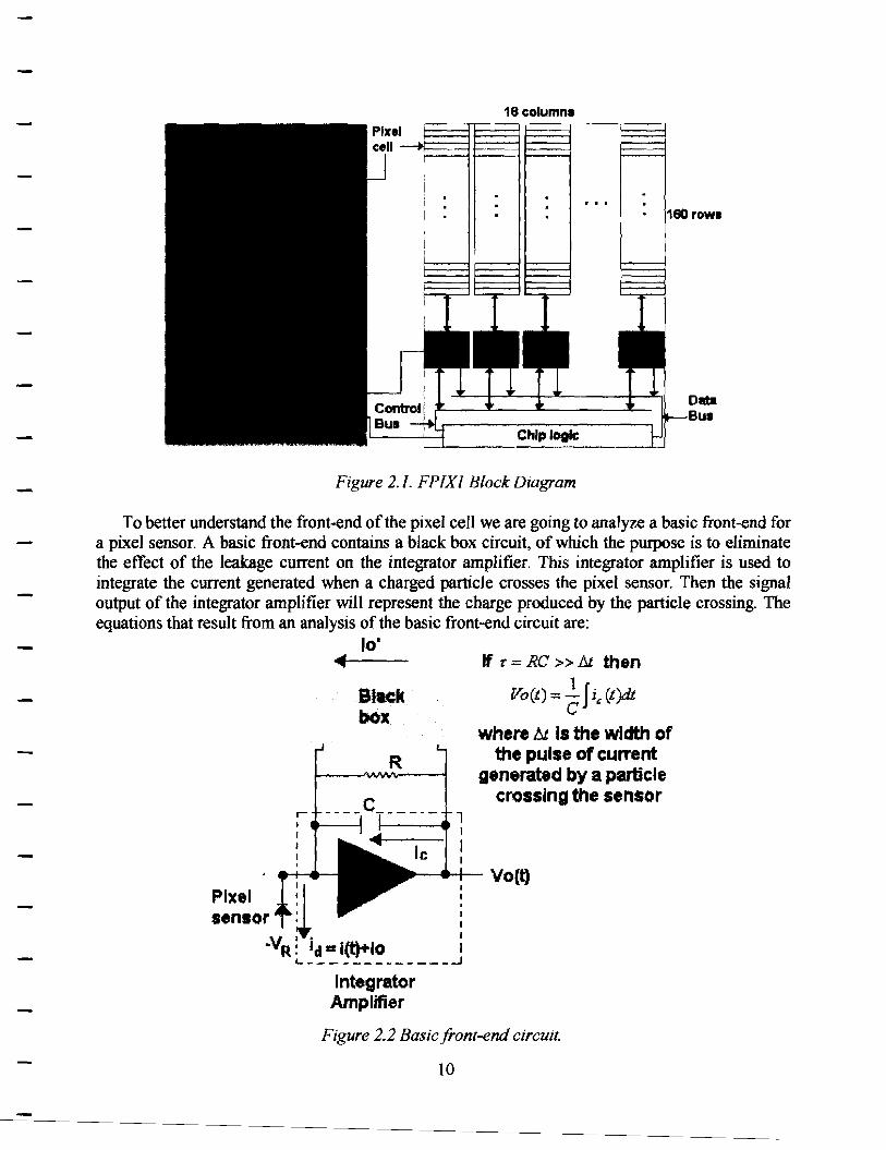
FPIXI is the second in the sequence of submissions aimed at developing a chip that meets the BTeV requirements. It is a VLSI chip with pixel unit cells of size50µm x 400µm arranged in an array of 160 rows by 18 colwnns for a total of 2880 pixel cells. The readout and control architecture is column based. The block diagram of the FPIX I chip and a photograph of the chip are shown in Fig.2. l [5]. The FPIXI chip can be divided into three mutually dependent parts, the pixel cell, the End of Column {EOC) Logic and the Chip Control Logic.
9
18columns
160row1
Chip !ogle
Figure 2.1. FPIXJ Block Diagram
Data Bus
To better understand the front-end of the pixel cell we are going to analyze a basic front-end for a pixel sensor. A basic front-end contains a black box circuit, of which the purpose is to eliminate the effect of the leakage current on the integrator amplifier. This integrator amplifier is used to integrate the current generated when a charged particle crosses the pixel sensor. Then the signal output of the integrator amplifier will represent the charge produced by the particle crossing. The equations that result from an analysis of the basic front-end circuit are:
lo'
Slack box
R
r I
I
C______ 1 ---1 I
I I
I le
Pixel ~ 1 sensor : : 'I.I I • I -vR: 1d a i(t)+lo I
L-- - - - - - - - - - - _ ..J
Integrator Amplifier
If r = RC >> & then
Vo(t) = ~ J if: (t)dt
where !Jt is the width of the pulse of current
generated by a particle crossing the sensor
Figure 2.2 Basic front-end circuit.
10

Performing node analysis we obtain:
-[i(t)+!o]+Io' +ic +iR =0 (2.1)
where i(t) is the current generated by the particle crossing, Io is the leakage current and Io' is the black box current. Then this equation can be divided in two cases the de and the ac cases, for the de case we have:
- Jo+ Io' = 0 ; Jo' = lo (2.2)
In consequence the current that flows by the black box must be equal to the leakage current denominated by Io. This condition is necessary and means that the leakage current doesn't flow thought the integrator amplifier. For the ac case we have:
(2.3)
and
. _ C dVo(I). . _ Vo(I) IC - / ,IR -
dt R (2.4)
where Vo(t) is the voltage output of the integrator amplifier. This voltage will be a pulse generated by the particle crossing. Taking the integral on both sides of the equation we have:
i(t) == dVo(t) + Vo(ll dt RC
(2.5)
Solving the differential equation we can obtain the natural response, setting the current i(t) equal to zero:
Vo,,(I) =Vo ex{- ;C) (2.6)
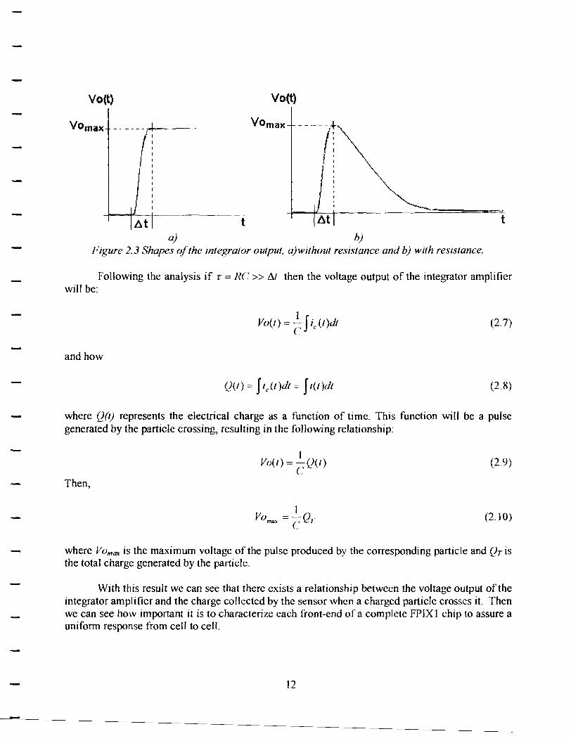
Then we can assume that the action of the resistor is to discharge the capacitor after the current generated by the particle crossing the sensor is integrated. If we don't put the resistance in the circuit then the capacitor always will be charged, i.e., if other particle crosses the sensor then the amplifier doesn't integrate the charge from zero. Instead the amplifier will begin to integrate the charge starting from the voltage level that has the capacitor, which is the level of the maximum voltage output of the amplifier produced by the first particle. With the incorporation of a resistance in the circuit we are avoiding this problem. For better understanding we show in figure 2.3 the shape of the integrator output without and with this resistance.
11
Vo(t) Vo(t)
-- ---- .... ~----
( 1
I
-----+
fl I
At t .6.t t
a) h) Figure 2.3 Shapes ~lthe integrator output, a)without resistance and b) with resistance.
Following the analysis if r = RC>> l!.t then the voltage output of the integrator amplifier will be:
Vo(l) = :~ J ic (l)dl (2.7)
and how
Q(I) == J ic<t)dt = J i(t)dt (2.8)
where Q(t) represents the electrical charge as a function of time. This function will be a pulse generated by the particle crossing, resulting in the following relationship:
Then,
t Vo(I) = _rJ(t) c;: (2.9)
(2.10)
where Vom~ is the maximum voltage of the pulse produced by the corresponding particle and Qr is the total charge generated by the particle.
With this result we can see that there exists a relationship between the voltage output of the integrator amplifier and the charge collected by the sensor when a charged particle crosses it. Then we can see how important it is to characterize each front-end of a complete FPIX t chip to assure a uniform response from cell to cell.
12
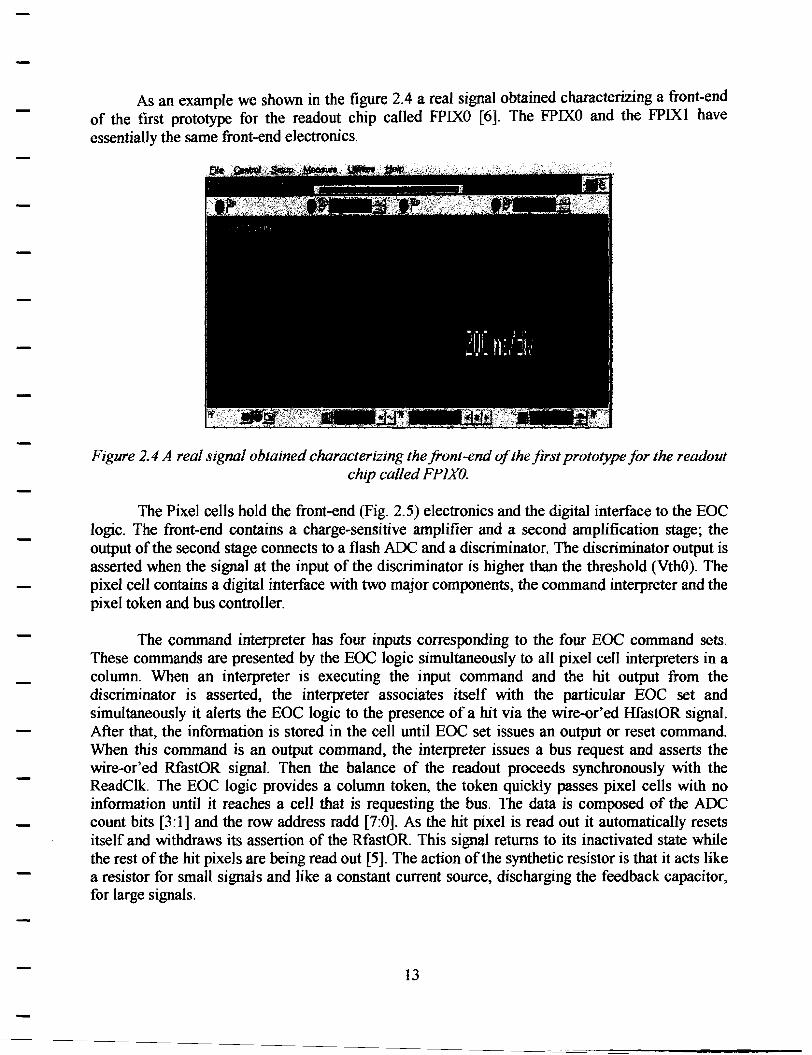
As an example we shown in the figure 2.4 a real signal obtained characterizing a front-end of the first prototype for the readout chip called FPIXO [6]. The FPIXO and the FPIXI have essentially the same front-end electronics.
Figure 2. 4 A real signal obtained characterizing the front-end of the first prototype for the readout chip called FPIXO.
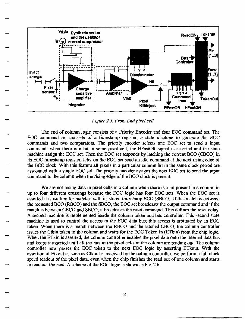
The Pixel cells hold the front-end (Fig. 2.5) electronics and the digital interface to the EOC logic. The front-end contains a charge-sensitive amplifier and a second amplification stage; the output of the second stage connects to a flash ADC and a discriminator. The discriminator output is asserted when the signal at the input of the discriminator is higher than the threshold (VthO). The pixel cell contains a digital interface with two major components, the command interpreter and the pixel token and bus controller.
The command interpreter has four inputs corresponding to the four EOC command sets. These commands are presented by the EOC logic simultaneously to all pixel cell interpreters in a column. When an interpreter is executing the input command and the hit output from the discriminator is asserted, the interpreter associates itself with the particular BOC set and simultaneously it alerts the EOC logic to the presence of a hit via the wire-or'ed HfastOR signal. After that, the information is stored in the cell until EOC set issues an output or reset command. When this command is an output command, the interpreter issues a bus request and asserts the wire-or' ed RfastOR signal. Then the balance of the readout proceeds synchronously with the ReadClk. The EOC logic provides a column token, the token quickly passes pixel cells with no information until it reaches a cell that is requesting the bus. The data is composed of the ADC count bits [3:1] and the row address radd [7:0]. As the hit pixel is read out it automatically resets itself and withdraws its assertion of the RfastOR. This signal returns to its inactivated state while the rest of the hit pixels are being read out [5]. The action oftbe synthetic resistor is that it acts like a resistor for small signals and like a constant current source, discharging the feedback capacitor, for large signals.
13
Vdda Synthetic rnltor and the Leakage
Irr current suppressor
r--1
Inject ' I
ch~ i__/e-+-' ........, Plxel
Integrator Plxel J KlllRnject RFastOR HFutOR
Figure 2.5. Front End pixel cell.
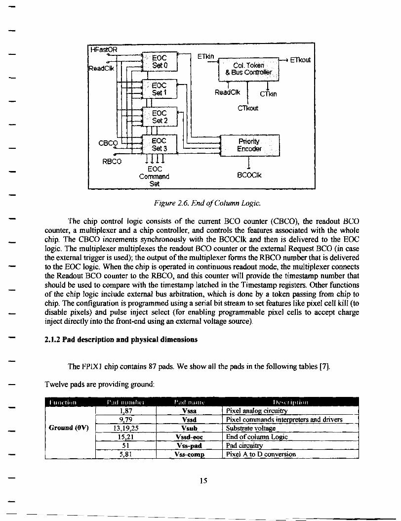
The end of column logic consists of a Priority Encoder and four EOC command set. The EOC command set consists of a timestamp register, a state machine to generate the EOC commands and two comparators. The priority encoder selects one EOC set to send a input command; when there is a hit in some pixel cell, the HFastOR signal is asserted and the state machine assign the EOC set. Then the EOC set responds by latching the current BCO (CBCO) in its EOC timestamp register, later on the EOC set send an idle command at the next rising edge of the BCO clock. With this feature all pixels in a particular colwnn hit in the same clock period are associated with a single EOC set. The priority encoder assigns the next EOC set to send the input command to the column when the rising edge of the BCO clock is present.
We are not losing data in pixel cells in a column when there is a hit present in a column in up to four different crossings because the EOC logic has four EOC sets. When the EOC set is asserted it is waiting for matches with its stored timestamp BCO (SBCO). If this match is between the requested BCO (RBCO) and the SBCO, the EOC set broadcasts the output command and if the match is between CBCO and SBCO, it broadcasts the reset command. This defines the reset delay. A second machine is implemented inside the column token and bus controller. This second state machine is used to control the access to the EOC data bus; this access is arbitrated by an EOC token. When there is a match between the RBCO and the latched CBCO, the column controller issues the Ctkin token to the column and waits for the EOC Token In (ETkin) from the chip logic. When the ETkin is asserted, the column controller enables the pixel data onto the internal data bus and keeps it asserted until all the hits in the pixel cells in the column are reading out. The column controller now passes the BOC token to the next EOC logic by asserting ETkout. With the assertion of Etkout as soon as Ctkout is received by the column controller, we perfonn a full clock speed readout of the pixel data, even when the chip finishes the read out of one column and starts to read out the next. A scheme of the EOC logic is shown as Fig. 2.6.
14
ReadClk
RBCO EOC
Command Set
CoLToken & Bus Controller
ReadClk CTl<in
CTkout
Priority Encoder
BCOClk
ETkout
Figure 2.6. End of Column Logic.
The chip control logic consists of the current BCO counter (CBCO), the readout BCO counter, a multiplexer and a chip controller, and controls the features associated with the whole chip. The CBCO increments synchronously with the BCOClk and then is delivered to the EOC logic. The multiplexer multiplexes the readout BCO counter or the external Request BCO (in case the external trigger is used); the output of the multiplexer forms the RBCO number that is delivered to the EOC logic. When the chip is operated in continuous readout mode, the multiplexer connects the Readout BCO counter to the RBCO, and this counter will provide the timestamp number that should be used to compare with the timestamp latched in the Timestamp registers. Other functions of the chip logic include external bus arbitration, which is done by a token passing from chip to chip. The configuration is programmed using a serial bit stream to set features like pixel cell kill (to disable pixels) and pulse inject select (for enabling programmable pixel cells to accept charge inject directly into the front-end using an external voltage source).
2.1.2 Pad description and physical dimensions
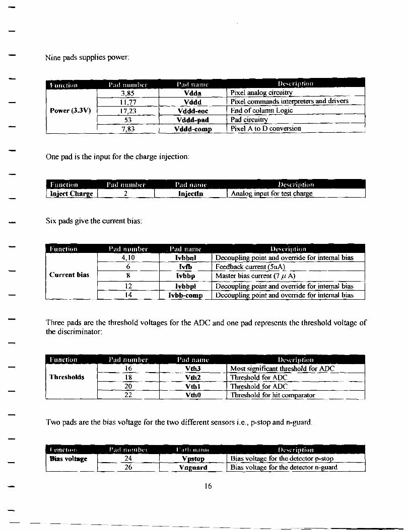
The FPIXl chip contains 87 pads. We show all the pads in the following tables [7].
Twelve pads are providing ground:
I 1111i:ti•111 l',td 1111111hr1 l',id ll,lllll' I h''( 1 iprion 1,87 Vssa Pixel analog circuitrv 9,79 Vssd Pixel commands intemreters and drivers
Ground (OV) 13,19,25 Vsub Substrate voltrule 15,21 Vssd-eoc End of column Lotric
51 Vss-pad Pad circuitrv 5,81 Vss-conip Pixel A to D conversion
15
Nine pads supplies power:
I· unl·tion Pad nu m her l'ad name rk-.rriptio11
3,85 Vdda Pixel analog circuittv 11,77 Vddd Pixel commands interoreters and drivers
Power (3.JV) 17,23 Vddd-eoc End of column Logic 53 Vddd-pad Pad circuitry
7,83 Vddd-comp Pixel A to D conversion
One pad is the input for the charge injection:
~111141t111,1111111111o;~W1.llBl!ii ~lJMHMit'~ In ect Cha e 2 Iniectln Analo m ut for test char e
Six pads give the current bias:
Function Pad number Pad name l>r'lTi pt ion 4,10 Ivbbnl Decoupling point and override for internal bias
6 lvfb Feedback current (5nA) Current bias & lvbbp Master bias current (7 µ A)
12 I vb bpi Decoupling point and override for internal bias 14 lvbb-comp Decoupling point and override for internal bias
Three pads are the threshold voltages for the ADC and one pad represents the threshold voltage of the discriminator:
Funl·tion Pad numbe1· 1':1d name Dl''l' ription 16 VthJ Most significant threshold for ADC
Thresholds 18 Vth2 Threshold for ADC 20 Vthl Threshold for ADC 22 VthO Threshold for hit comparator
Two pads are the bias voltage for the two different sensors i.e., p-stop and n-guard.
16
Fifteen control signals, which we can program, control and readout the FPIXl chip:
27/28 29
30 Control 31 signals 32
33 34/35 36/37
50 76,78,80
Thirty-two output signals
Output signals 82
38-49, 54-75 84/86
Tokenln!f okenln* In ut for the chi token TrigAcc Trigger mode: Trigger signal; Continous
mode: A t 3.3V or re"ect OV hits. Shiftln
DataRes Pr ramlles
ShiftClk ReadClk*/ReadClk The read out clock BCOClk*IBCOClk
Data outputs 17 differential si nals TokenOut*ffokenOut
The size of the FPIXI chip is 7.Smm by 12.Smm (4]. Pads 1 and 87 are 17.3 microns in from the outer edge ofFPIXl. The bottom row of pads, which are the odd number pads, are 39.2 microns from the bottom ofFPIXl. The FPIXl pads are on a 169.2 micron pitch with 79.2 microns between pads, the pads themselves are 160 microns by 90 microns. A sketch is shown in fig. 9. A block diagram of the FPIXl chip is shown as a Fig.2.7.
39.2µ.m 7.6mm
, .. .JJ Q.,pm ~ [1[~ ~ 160µ.m - i 9.
90µ.m ; i.-ti--
169.2µ.m
Figure 2. 7. FPIXJ physical dimensions.
17
The most important signals are the control signals. With these signals we can do~load information to the chip. Most of these control signals are CMOS i.e., 3.3V represents a logical l and OV represents a logical 0. The first control signals are Reg [2:0] that represent the scan path selectors for the Sbiftln signal; they are CMOS inputs. Shiftln is a CMOS input for the scan paths. At the rising edge of the SbiftClk, the value at the Sbiftln will be scanned into the path chosen by the RegO, Regl, and Reg2 signals. SbiftClk is the clock signal; at the rising edge the contents of the Shiftln signal are scanned into whatever scan path is selected by RegO, Regl, and Reg2 signals. DataRes is a reset level signal. When this signal is high, the BCO counters are reset to zero; the End of column registers are reset to empty and the chip stops outputting data. ProgramRes is a reset level signal. When this signal is high, the mask registers are set to zero; the chip is reset to continuous mode; the BCO lag is set to 2 and the ChipID is set to zero. LoadKill is the signal which latches the kill pattern that has been scanned into the pixel array on its falling edge. It is a CMOS level signal and it is kept at logical 1 during the kill scan, and dropped to a logical 0 to latch the kill pattern. TrigAcc is a dual-mode signal. If the chip is operating in triggered mode, it is the trigger signal. If the chip is operating in continuous mode, this pad is the Accept/Reject signal. In continuous mode, when this signal is logical 0 the chip rejects (ignores) incoming data, and when is logical 1 the chip accepts incoming data. This is a single ended CMOS signal.
To get the information acquired by the chip, we need to send the set of signals that control the readout of the chip information and then process it. Most of these signals are low voltage differential signals, or L VOS, (Vhi = I. 75V; Vlo=: l.55V). ReadClk*/ReadClk is a free-running L VOS level differential clock. The simulated frequency was 26MHz, but the real frequency will be whatever the chip can handle. BCOClk*/BCOClk is an L VDS representation of the beam crossover signal. Tokenlnffokenln* it is an L VDS input. When the signal is high (Pad 27=1.75V; Pad 28=1.55V), the chip can take the bus. When this signal is low (Pad 27=1.55V; Pad 28= l. 75V), the chip cannot take the bus and its data outputs are tri-stated.
The ShiftOut represents the scan output for each of the scan paths selected by RegO, Regl and Reg2. This signal is a CMOS level. This signal will be driven to the Shiftln of the next chip when you connect several chips in daisy chain. TokenOut*ffokenOut represents the output of the chip token signal.
The FPIXl chip delivers its information in the following data output format [7]. The data outputs are tri-statable L VOS outputs. Data 16 is the data valid signal; with this signal you can know if the chip has data to send. When the chip has data, the Data valid signal will be a logical l (3.JV) if there are no data this signal will be a logical 0 (OV). When there are data available, it will come in two forms i.e., control and data words; by means of Data 15 we can know whether the word presented is a control or a data word. Data 15 is a logical 0 in a control word and a logical 1 in a data word. The control word contains the ChipID of the chip and the BCO number (time stamp). The data word contains the row address, column address and magnitude (ADC value) of a particular hit pixel. In the table 2 we show all data and its corresponding meaning.
18
Pad nanw Pad-. numbr1· Data ·\\ ailahk Data -\' ailahk
Control \\ onl Data \\ onl
Data 16/Data 16* 74/75 Logical I L all og1c
Data 15/DatalS"' 73/72 Logical 0 Logical l
Data 14/Data 14* 71/70 Logical 0 ADC [I]
Data 13/Data 13* 69/68 Logical 0 ADC {Ol
Data 12/Data 12* 67/66 Logical 0 Col Addr f4l
Data 11/Data 11 * 65/64 ChipID ro1 Col Addr f3l
Data 1 O/Data 1 O* 63/62 ChieID [O] Col Addr [21 Data 9/Data 9* 61/60 ChipJD [O] Col Addr [11
Data 8/Data 8* 59/58 ChiplD [Ol Col Addr J01
Data 7/Data 7* 57/56 Logical 0 Row Addr Pl Data 6/Data 6* 55/54 Logical 0 Row Addr f6l Data 5/Data 5* 49/48 BCO l5] Row Addr f5l Data 4/Data 4* 47/46 BCO f41 Row Addr [4] Data 3/Data 3* 45144 BCO f31 Row Addr (31 Data 2/Data 2 * 43/42 BCO [2] Row Addr f2l Data I/Data 1 * 41/40 BCO Ill Row Addr fll Data O/Data O* 39/38 BCO [O] Row Addr (OJ
Table 2. Data outputs from the FPIXI chip.
2.1.3 Scan paths and Readout
There are eight different control sequences by which we can download infonnation to the FPIXl chip. These are called scan paths and are formed by shift registers with different depths in the FPIXl. Shift registers are a type of sequential logic circuit, mainly used for the storage of digital data. They are a group of flip-flops connected in a chain so that the output from one flipflop becomes the input of the next flip-flop. Most registers used in this way possess no characteristic internal sequence of states. All the flip-flops are driven by a common clock and all are set or reset simultaneously. A basic four-bit shift register can be constructed using four D flipflops, as shovvn in Fig.2. 8. The operation of the circuit is as follows. The register is first cleared, forcing all four outputs to zero. The input data is then applied sequentially to the D input of the first flip-flop on the left (FFO). During each clock pulse, one bit is transmitted from left to right. Assume a data word to be 1001. The least significant bit of the data has to be shifted through the register from FFO to FF3.
D<Jt<~ input
; .. -~Lt\
FFO FF1 FF2 FF3 D sE< Q D 6E< Q D
6E<
Q D SET Q
CIA Q CIA Q CIA Q CIA Q
I F~O I F~1 I F~2 I F~3 I Figure 2.8. A hasicfiJur-bit shift register
19
Data output
Clear
To choose a particular scan path [7] we select one of the eight different codes using the control signals named RegO, Regl, and Reg2. For example to configure the chip, you must select the code IOI. The codes are given in Table 3. To load all the scan paths into the chip, we are use the same Shiftln pad, the same SbiftClk pad and the same SbiftOut pad. There is necessary time a relationship between Shiftln and SbiftClk signals. Sbiftln must be delayed by more than 5ns from ShiftClk.
2 0 I 0 Not used 3 0 I I Pro ammable reset del 4 100 Not used 5 I 0 I 6 I I 0
7 I I l
Table 3. Scan paths to program the FPIXI chip.
A brief description the register codes for selection of each of the scan paths is as follows: The idle path should be the default path, if no action is taken Reg2, Regl and RegO should be set to 000. The paths selected by 010 and I 00 instruct the chip to take no action as for the idle path. The trigger path code is 00 I and you select this if you want to use the chip in external trigger mode. This path is six bits deep, and the most significant bit is scanned in first. When all six bits have been scanned in, a pulse on the TrigAcc pin (pad 29) will produce a new trigger request to the end of column logic cells.
The code to select programmable reset delay path is 011. Each EOC logic circuit has a mask register that is six bits deep. When all the bits in the mask register are equal to zero the EOC logic will reset itself in 64 BCO clock cycles. When all bits in the mask register are set to one, the column is effectively shut down. This scan path is I 02 bits long because each column has a 6 bits mask register in its EOC logic circuit, this means 6x 17= 102 bits. Then, e.g., you send 102 bits of zeros to do a reset delay by means of the Sbiftln pad. The most significant bit of column 17 is scanned in first; the least significant bit of column I is scanned in last.
The register code for the configure path is I 0 I. This path is used to program the mode of operation of the chip, the identification number (ChipID) and the BCO lag number. There are two modes of operation, triggered mode or continuous mode. If you enter a logical 1 (3.3V) into the pattern you select triggered mode, while if you enter a logical 0 (OV) you select a continuous mode. The ChipID number is the identification number of the chip. If you are working with one chip, you can give it any identification number, e.g., 0000. If you have more than one chip, as on the MCM, you need to identify the chip from which you are receiving information. The BCO lag is the minimum distance between the current BCO number and the requested BCO number in continuous mode. Typically, this number is set to two. The configure path contains 11 bits, 1 bit for the mode of operation, 4 bits for the ChiplD number and 6 bits for the BCO lag. Then, by means of the Shiftln pad you need to send 11 bits with the configuration that you want. The most significant bit
20
of the BCO lag is scanned in first, followed by the rest of the BCO Jag. Then the most significant bit of the ChipID is scanned in. Finally, the mode of operation is scanned in.
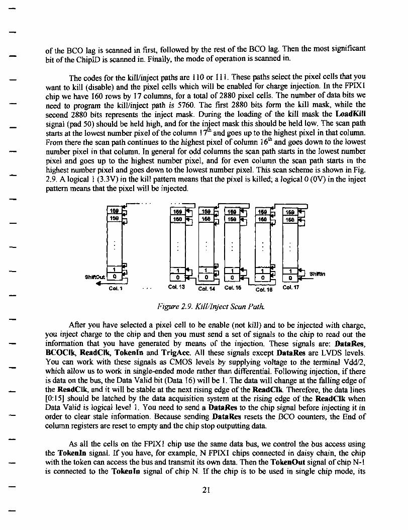
The codes for the kill/inject paths are 110 or I 11. These paths select the pixel cells that you want to kill (disable) and the pixel cells which will be enabled for charge injection. In the FPIX 1 chip we have I 60 rows by I 7 columns, for a total of 2880 pixel cells. The number of data bits we need to program the kill/inject path is 5760. The first 2880 bits form the kill mask, while the second 2880 bits represents the inject mask. During the loading of the kill mask the LI>ad.Kill signal (pad 50) should be held high, and for the in~ect mask this should be held low. The scan path starts at the lowest number pixel of the column 17 and goes up to the highest pixel in that column. From there the scan path continues to the highest pixel of column 16th and goes down to the lowest number pixel in that column. In general for odd columns the scan path starts in the lowest number pixel and goes up to the highest number pixel, and for even column the scan path starts in the highest number pixel and goes down to the lowest number pixel. This scan scheme is shown in Fig. 2.9. A logical 1 (3.3V) in the kill pattern means that the pixel is killed; a logical 0 (OV) in the inject pattern means that the pixel will be injected.
Col.17
Figure 2.9. Ki/11Tnject Scan Path.
After you have selected a pixel cell to be enable (not kill) and to be injected with charge, you inject charge to the chip and then you must send a set of signals to the chip to read out the information that you have generated by means of the injection. These signals are: DataRes, BCOCl.k, ReadClk, Tokenln and TrigAcc. All these signals except DataRes are L VDS levels. You can work with these signals as CMOS levels by supplying voltage to the terminal V dd/2, which allow us to work in single-ended mode rather than differential. Following injection, if there is data on the bus, the Data Valid bit (Data 16) will be 1. The data will change at the falling edge of the ReadClk, and it will be stable at the next rising edge of the ReadClk. Therefore, the data lines [0:15] should be latched by the data acquisition system at the rising edge of the ReadClk when Data Valid is logical level 1. You need to send a DataRes to the chip signal before injecting it in order to clear stale information. Because sending DataRes resets the BCO counters, the End of column registers are reset to empty and the chip stop outputting data.
As all the cells on the FPIXl chip use the same data bus, we control the bus access using the Tokenln signal. If you have, for example, N FPIXI chips connected in daisy chain, the chip with the token can access the bus and transmit its own data. Then the TokenOut signal of chip N-1 is connected to the Tokeoln signal of chip N. If the chip is to be used in single chip mode, its
21
Tokenln can be set to a logical I. Finally, the chip will accept hits if the TrigAcc signal is logical level 1, and will reject hits if this signal is logical level 0.
2.1.4 Design of patterns to control the FPIXl chip
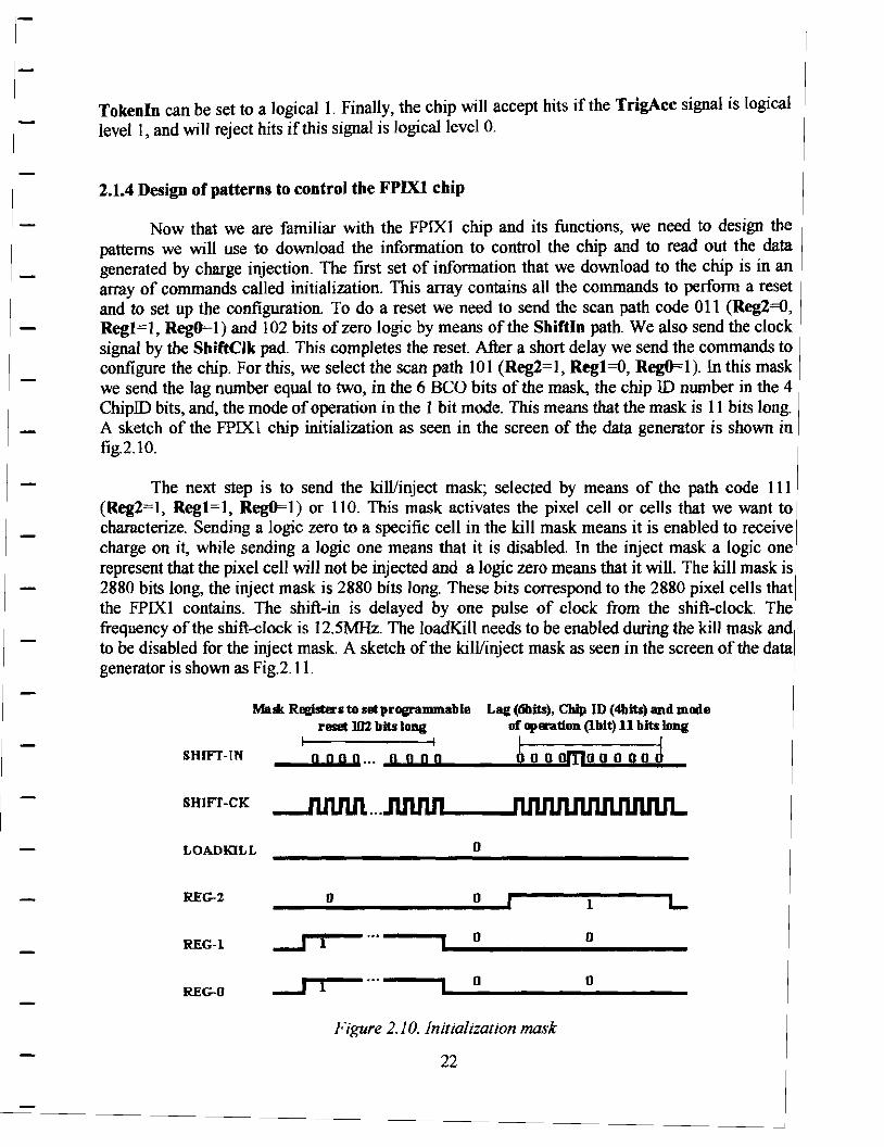
Now that we are familiar with the FPIXI chip and its functions, we need to design the patterns we will use to download the information to control the chip and to read out the data generated by charge injection. The first set of information that we download to the chip is in an array of commands called initialization. This array contains all the commands to perform a reset and to set up the configuration. To do a reset we need to send the scan path code OII (Reg2=0, Regl=l, RegO=l) and 102 bits of zero logic by means of the Shiftln path. We also send the clock signal by the ShiftClk pad. This completes the reset. After a short delay we send the commands to configure the chip. For this, we select the scan path 101 (Reg2=1, Regl=O, Reg&=l). In this mask we send the lag number equal to two, in the 6 BCO bits of the mask, the chip ID number in the 4 ChipID bits, and, the mode of operation in the 1 bit mode. This means that the mask is 11 bits long. A sketch of the FPIXl chip initialization as seen in the screen of the data generator is shown in fig.2.10.
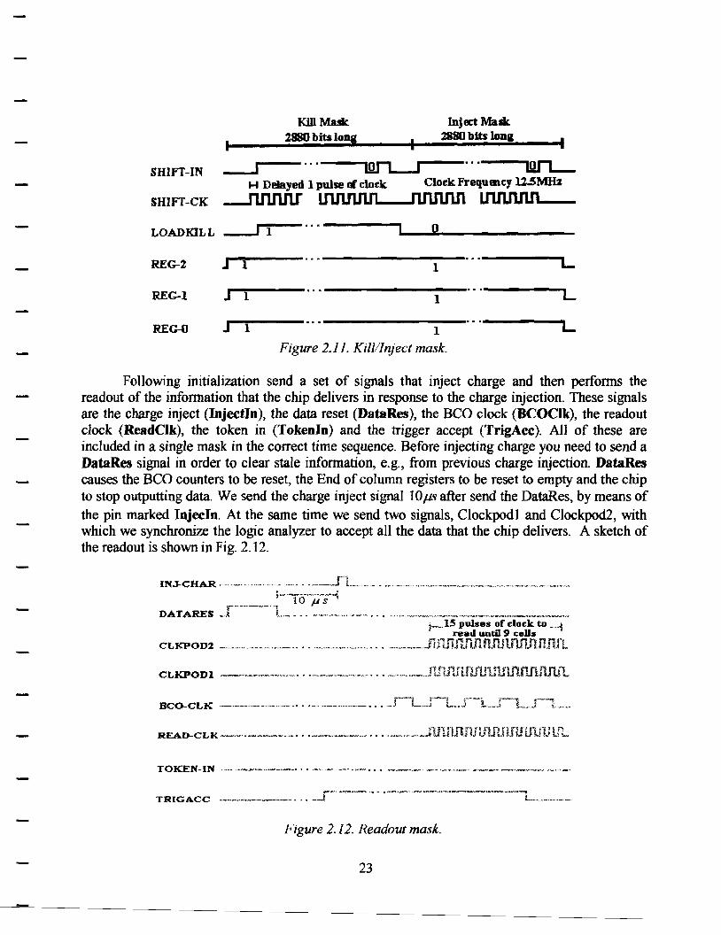
The next step is to send the kill/inject mask; selected by means of the path code 111 (Reg2=1, Regl=l, RegO=l) or 110. This mask activates the pixel cell or cells that we want to characterize. Sending a logic zero to a specific cell in the kill mask means it is enabled to receive charge on it, while sending a logic one means that it is disabled. In the inject mask a logic one represent that the pixel cell will not be injected and a logic zero means that it will. The kill mask is 2880 bits long, the inject mask is 2880 bits long. These bits correspond to the 2880 pixel cells that the FPIXl contains. The shift-in is delayed by one pulse of clock from the shift-clock. The frequency of the shift-clock is 12.5MHz. The loadKill needs to be enabled during the kill mask and to be disabled for the inject mask. A sketch of the kill/inject mask as seen in the screen of the data generator is shown as Fig.2.1 I.
Ma* Rea;isters to set prOVclmmable Laa (libits), Chip ID (4bits) and mode reset 102 bits long of operation (lblt) 11 bits long
SHIFT-IN Q Q Q Q ..... g....,.g..,g._.g..._ __ ...:i;4..::o:...:o~orno o o o o J SHIFT-CK n., n.,
--ILll.ILIL ...
LOAD KILL 0
REG-2 0 0 1 L
REG-1 __rr--··· I 0 0
REG-0 __rr--··· 0 0
Figure 2.10. Initialization mask
22
Kill Mask Inject Mark
1 2880 bits lon1 I 2S80 bits lona I
SHIFT-IN _r--···~···~ H Delayed I pulse of clock Clock Frequmcy ll.5Mlh
SHIFT-CK __nnrutr l11IUlflJL-..
LOAD KILL __rr---··· 0
REG-2 J l l L
REG-I J 1 I L
REG-0 J l 1 L Figure 2.11. Kill/Inject mask.
Following initializ.ation send a set of signals that inject charge and then perfonns the readout of the infonnation that the chip delivers in response to the charge injection. These signals are the charge inject (Injectln ), the data reset (DataRes ), the BCO clock (BCOClk), the readout clock (ReadClk), the token in (Tokenln) and the trigger accept (TrigAcc). All of these are included in a single mask in the correct time sequence. Before injecting charge you need to send a DataRes signal in order to clear stale infonnation, e.g., from previous charge injection. DataRes causes the BCO counters to be reset, the End of colwnn registers to be reset to empty and the chip to stop outputting data. We send the charge inject signal 10 µs after send the DataRes, by means of the pin marked Injecln. At the same time we send two signals, Clockpodl and Clockpod.2, with which we synchroniz.e the logic analyzer to accept all the data that the chip delivers. A sketch of the readout is shown in Fig. 2.12.
READ-CL I<.---·--···--·-·-'-----~· .• -----"-· - ... __ ._.,, ........ JU1JUU1Jlftf'w111J1H.mlfl.
TRIGACC
Figure 2.12. Readout mask.
23

2.2 THE MULTI CHIP MODULE (MCM)
The innennost detector for the BTeV experiment will be a pixel detector. This detector will be composed by 62 pixel planes, and each plane contains several pixel chips bump bonded to the sensors. A very important constraint associated with these planes is their mass. They should be as light as possible to decrease particle interactions with the material. Particle interactions cause scattering and thus increase the error in the reconstruction of the trajectories of the particles. Other important constraints related to the pixel detector are that they must work in a high radiation environment and in vacuum. The detector will suffer a substantial radiation dose, which means that it has to be built with material and glues that are radiation hard. Also they cannot outgas or evaporate in vacuum. Since the detector is inside vacuum, most of the heat has to be conducted from the chips to liquid cooling channels placed in the support material. In this case carbon fiber structures are good candidates because they provide lower mass associated with good thennal conductivity and are none the less structurally sound. For all these reasons the experiment decided to glue high density interconnect (HDI) circuits on the top of a carbon fiber plate that holds the detector and associated electronics. The cooling channels are embedded in the plate and are also made from carbon that has been fused into glassy tubes. The readout and control chips will be wire bonded to the HDI.
2.2.1 High Density Interconnect Circuits (HDI)
In the new world of electronics the HDI has gained a very high importance. The trend toward miniaturization and toward higher and higher speed devices has increased the demand for smaller and smaller semiconductor components with an even increasing density of input-output signals as well as a demand for a higher number of connection points on the printed circuit boards (PCB) on which the chips are mounted. Multi-layer flex circuits will provide the interconnection densities needed to meet the demands for the BTeV experiment.
The flex circuit contains four layers, two layers for signal interconnects, one layer for power and other signals and one layer for the ground plane [4]. There are two ways to proceed in order to produce the flex circuit. One is to use a four circuit layer flex circuit, and the other is to use two flex circuits, each with two layers and one assembled on the top of the other. Other approaches can also be considered, like one with two flex circuits with differing densities, one assembled on the top of the other. This idea is based on the fact that just portion of the circuit requires high density interconnect. The first circuit would be two layer flex circuit layout using '"standard" design rules (with 100µm minimum traces and spaces widths, 400µm via cover pads and 200µm via through holes). The second flex, which would be built using more "aggressive" design rules {like 25µm traces widths and 68µm via cover pads), is used for the siblJlal interconnects. In our application, this two rule flex circuit could be employed in the following way: the "standard" rule circuit would be used for the power and ground planes and some other low density signals, while the "aggressive" rule circuit would be used for the signal interconnects. This approach also requires that there not be many interconnections between the two different rule circuits, which is probably the case for BTeV. We interconnect efficiently from circuit to circuit, using wire bonds. Furthennore, this approach, using two different design rule circuits, lends itself to an important perfonnance improvement, namely mass reduction. Also it may be possible to find some vendor wil1ing to
24
manufacture "standard" rule flex circuit with aluminum conductors, since aluminum is a lower Z material than copper and therefore causes much less scattering.
2.2.2 Operation of the MCM
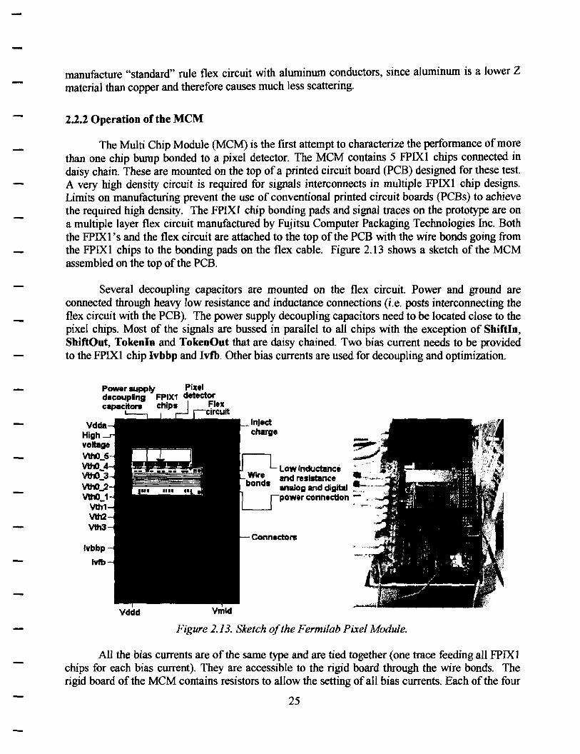
The Multi Chip Module (MCM) is the first attempt to characterize the performance of more than one chip bump bonded to a pixel detector. The MCM contains 5 FPIXl chips connected in daisy chain. These are mounted on the top of a printed circuit board (PCB) designed for these test. A very high density circuit is required for signals interconnects in multiple FPIXl chip designs. Limits on manufacturing prevent the use of conventional printed circuit boards (PCBs) to achieve the required high density. The FPIXl chip bonding pads and signal traces on the prototype are on a multiple layer flex circuit manufactured by Fujitsu Computer Packaging Technologies Inc. Both the FPIXl 'sand the flex circuit are attached to the top of the PCB with the wire bonds going from the FPIXl chips to the bonding pads on the flex cable. Figure 2.13 shows a sketch of the MCM assembled on the top of the PCB.
Several decoupling capacitors are mounted on the flex circuit. Power and ground are connected through heavy low resistance and inductance connections (i.e. posts interconnecting the flex circuit with the PCB). The power supply decoupling capacitors need to be located close to the pixel chips. Most of the signals are bussed in parallel to all chips with the exception of Shiftln, ShiftOut, Tokenln and TokenOut that are daisy chained. Two bias current needs to be provided to the FPIXl chip Ivbbp and lvtb. Other bias currents are used for decoupling and optimization.
Power supply Pixel decoupling FPIX1 detector capacitors chips ~lex
Vdda High voltage vth0_5 VltlO_ Vlt10_3 vth0..,.2 W.0_1
Vth1 Wl2 vth3
Vddd
circuit
Vmld
Inject charge
Low Inductance ·· and resistance •-,,.:_~ .. , analog and digital ~:-:-- · -power connection - · .
Connectors
Figure 2.13. Sketch of the Fermi/ab Pixel Module.
All the bias currents are of the same type and are tied together (one trace feeding all FPIXl chips for each bias current). They are accessible to the rigid board through the wire bonds. The rigid board of the MCM contains resistors to allow the setting of all bias currents. Each of the four
25

threshold voltages, VthO, Vthl, Vtb2, and Vtb3, are also be tied together through the conn~ct~r. The thresholds need also to be decoupled by capacitors mounted on the top of the flex cucu1t. There will be 324 microns between the centers of the outside pads of two adjoining FPIXI chips. Figure 2.14 shows a block diagram of the flex circuit and a photograph.
FPIX1 Chip t
Shift Shiftln1
Shlltak ·--~L oatlklll&Reg('J . .DJ
lnjCharge --Datares --Tngacc--BCOOk and Rea~Qk
Tluesholdt & 1 Oat8']:16J ...,.-
f oken0ut5 · Shifl0ut5
Figure 2.14. Block diagram of the flex circuit and a photograph.
Fujitsu Computer Packaging Technologies (FCPT) fabricated the flex circuit [8]. Because there are only 79.2 microns between pads a high density routing design is required in order to be able to route a trace between the outer row of pads of the FPIXl chip. Minimum trace widths are 20 microns with a minimum clearance of 20 microns. Vias are also be veiy small. In table 4 we are shown Fujitsu's design rules.
Via Hole Diameter 25 f.011
Via Cover Pad Diameter 108 f.011
Via Center Spacing 208 f.011
Via Cover Pad to Line Clearance 20µm
Line Width 20 f.011
Line to Line Clearance 20 f.011
Line Center Spacing 40µm
Table 4 FCTP 's design rules.
The two rows of pads on the FPIXI chip require a veiy high density design. The vias must be veiy small in order to fit between the traces. The traces need to be veiy small in order to permit the vias to be placed. A bus of top layer traces runs horizontally from the bonding pads that connect the flex circuit to the PCB. This bus of traces connects all of the common signals to the five FPIXI chips. The second layer has traces that connect the FPIXI chip signals to the bus. The trace widths are 20 microns with a 20 µn clearance. Vias will be 108 microns with a 25 micron hole sire. Layer 3 is a power plane for V ddd and V dda. Layer 4 is the ground plane.
26
The MCM operates like a single FPIXl, with the only difference that in the single FPIXI we only had 2880 pixel cells, and with the M:CM we have 14400 pixel cells. In the single FPIX l we found that the ShiftOut signal is inverted in relation of Shiftln. This presented a problem when we connected them in a daisy chain. To solve the problem we designed the mask in a special way to download information to the chips both for initialization and to select the cells to be characterized. The readout operates more or less like a single FPIXl. The only difference is in the Tokenln signal. You need to be careful setting this signal because if you don't keep this signal at logic high for a sufficient time to readout all five chips, you can lose all the information.
2.2.3 Design of patterns to control the MCM
We need to design the patterns in order to download the information to control the chip and to read out the information generated by an injection on a specific pixel cell to characterize it. Since in the MCM we have 5 chips connected in daisy chain, and the ShiftOut signal is inverted respect to Shiftln signal we need to send the mask in a specific format to avoid this problem. When you have only one chip on the module there is no problem, but when you add another chip, then you will have this problem, and to avoid it we decide to invert the logic of the commands, i.e. where you were sending a logic one to the first chip you need to send a logic zero to the second and vice verse. So we noticed that if we program an even number of chips we need to send the first mask in negative logic, and if we program an odd number of chips we need to send the first mask in positive logic. We synthesize this explanation in Table 3.
'iumlwr of FPI'\ I chip1; 1.ogic of th(' ma,f, l + 2 -+ 3 +-+ 4 -+-+ 5 +-+-+
Table 3. Format to send the masks in the MCM
The first set of information that we download to the chip is in an array of commands called initialization. This array contains all the commands to do a reset and the configuration. To do a reset we need to send the scan path code 011 (Reg2=<J, Regl =I, RegO= l) and l 02 bits of zero logic by means of the Shiftln pad, sending also the clock signal by the pad ShiftClk. Afterwards, we configure the FPlXl chip. So, we select the scan path code IOI (Reg2=1, Regl=<J, RegO=l ). In this mask we send the lag number equal to two, to fill the 6 BCO bits, the chip ID number using the 4 ChipID bits, and, the mode of operation that is 1 bit long. This means that the mask is 11 X5 bits long. A sketch of the FPIXl chip initialization is shown in fig.2.15.
27
SHIFT-IN
Mauk Registtrs to lt!t prlJll1llRlllable reset SlO (102D) btts Jong
no g g ... J 1 ... ,0 0 0 0
SHIFT-CK -fl.n.M ... JUUU' ...
Lag (tiblts), Cldp ID (4bits) and mode of op eratlon (lbit) 11 bits long per drip
b Q 0 cdI1IUlJI1o Q J h 1 l l WJiT'i1JUJil
LOADKILL Q
REG-? 0 0 l L
REG-I Q Q
REG-0 0 Q
Figure 2.15 Initialization mask for the MCM
Later on we need to send the kill/inject mask selected by means of the path 111 (Reg2= 1, Regl=l, RegO=l) or 110, which one we are selecting the pixel or pixel cells to be characterize. The kill mask is 14400 (2880x5) bits long, the inject mask is 14400 bits long. These bits correspond the 14400 pixel cells that the MCM contains. The format that we utilize to send these bits is as follows: the first 2880 bits are in positive logic, i.e., we send a zero logic in the kill mask to indicate that the specific pixel cell should be enabled to receive charge on it. Meanwhile we send logic one to indicate that a pixel cell should be disable. In the inject mask a logic one indicates that the pixel cell will not be injected and a logic zero that it will be. The second 2880 bits are in negative logic, that is the inverse logic of the first 2880 bits; the third are in positive logic; the fourth are in negative logic; and the fifth are in positive logic. The Shiftln is delayed one pulse of clock from the ShiftClk. The frequency of the shift-clock is 12.5MHz. The loadKill needs to be enabled during the kill mask and disabled for the inject mask. In figure 2.16 we show the kill/inject mask for the MCM.
KDI Mask Inject Mask
2flll hits Jonf I I I I 2880 hits long I I I PositlYe logil: NeptiYe lo&k Posidve logk Neplive logic
SHIFT-IN __rr--··· WJ'1 0 ... __m__r--···~ .. __:._m_ H Delayed l pube rt clock H Delayed l pulse m do.ck Clock. Frequmcy ll.5MHz Clock. Frequmey 12.5MHz
SHIFT-CK --Mllfl! lIUUlJ1n......M ll1JUUUL..JUUUU lJlJUU1JL._J1J1 tnnnn.n__
LOADKJLL _rr--...
REG-l J 1 1 l L
REC-1 J 1 1 1 L
J l 1 I L
Figure 2. 16 Kill/inject mask for the MCM
After the selection of the pixel cells by means of the kill/inject mask, we need to provide to the MCM all the commands to do the readout to get the information that the module delivers in response to the charge injected. These signals are the charge inject (Injectln ), the data reset
28
(DataRes), the BCO clock (BCOClk), the readout clock (ReadClk), the token in (Tokenln) and the trigger accept (TrigAcc ). All are contained in a special mask in a specific time sequence. Before sending the injection you need to send a DataRes signal in order to eliminate stale information. By sending a DataRes you perform a reset on the BCO counters, the End of column registers are reset to empty, and the chip stops outputting data. We send the charge inject signal IOµs after we send the DataRes, by means of the pin marked lnjecln. With these we are also sending two signals more, Clockpodl and Clockpod2, with which we synchronize the logic analyzer to accept all the data that the chip delivers. A sketch of the readout is shown in Fig 2.17.
IN.J.CHAR ... . •. ---1L_._, ... ··~·•·w••«•-. .----·~,.--~--"'W•··-~·· .. -·~-~-·~~"""'" ... "-··--·--· ···----·"--"~··--~-w~· ~a---sl
.-·-··~· _, µ DATARES .J L ... ·-··--"···,,··-···· ·---· ·---·---· -----·-· ... _____ _
CLKPOD2
r~~-~- o -~~-~,,~~-·-~~W·~"-"''~~~. ·~·-•.• -·---·-TRIGACC ·-·--·---·- · · · _ _; '--·-- .•. ----------
Figure 2. I 7 Readout mask for the MCM
2.3 CONCLUSIONS
We described the operation of the FPIXl chip and the MCM. Now we know how to handle these devices, and with this knowledge we are be able to perform tests on these prototype devices. In the following we will explain how to characterize the FPIXl chip and the MCM.
29
CHAPTER THREE
CHARACTERIZATION
We have developed a test stand for use in characterizing the FPIX I front-end electronics chips that are one version in the FPIX sequence of VLSI chips being developed at Fermi lab [5] for readout of the BTeV [2] pixel detector. This detector will provide highresolution space points near the interaction region for use in reconstructing tracks and vertices. The information the detector provides will be used in the first level trigger to select events that have a high probability to contain secondary decay vertices. This means that all of the hit information from every beam crossing must be made available to the trigger processors. A beam crossing occurs every 132 ns.
ln order to achieve the required resolution, ~ 9 µm, the pixel unit cells must not only be very small, 50µm by 400.wn, but the charge deposited in each must also be digitized and read out. The FPIX chips contain front-end electronics cells with the same dimensions as the pixels on the sensors. The number of FPIX chips which will be bump-bonded to each sensor will depend on the number of cells on each FPIX chip. The FPIXl version of the readout chips contains 2880 cells. Future iterations are expected to contain an even larger nwnber.
lf the readout is to be accomplished in the short time between crossings, the information must be sparsified so that only valid hit data is presented to the trigger processors. Which cells are read out is determined by a discriminator in each cell. If a signal above threshold is detected in the cell, then it is read out The threshold setting for all cells on a single FPIX chip is the same. On FPIX 1 it is set by a voltage input, called VthO, using an external supply. On the next iteration, the threshold will be set by means of a digital to analog converter. The test stand was built for the purpose of testing that the measured threshold (charge required to record a hit) and noise levels for the 2880
30
discriminators on the FPIXI chips were uniform enough that a single VthO for all of the cells would suffice. If there are significant cell to cell differences, then, since VthO must be set to a value well above the highest noise level measured, the charge information needed for accurate position measurements might be below the resulting charge threshold for some cells and would not be read out.
To gain experience on the technical issues involved in system integration, Fermilab has made a pixel-readout-chip sub-assembly containing five FPIXl chips called the Fermilab pixel multi-chip module (MCM). Five FPIXI chips have been integrated into a single module connected together by a flexible circuit, or High-Density Interconnect (HDI), made by Fujitsu Computer Packaging Technologies [8]. The tests described here were performed to characterize the 14,400 pixel cells contained on the five FPIXI chips in the MCM. The tests were performed to characterize the chips alone, i.e., without bumpbonding them to a pixel sensor and also with sensors on it.
3.1 BAD PIXEL MAP TEST
This is the first test that we carried out on the FPIXl chip to know the status of each pixel cell in the entire chip. The bad pixel map test is based on injecting charge into all cells on the chip to see what cells are working. First we program the FPIXI chip to kill all cells except seventeen. By testing seventeen at a time we are able to save time. Then the chip must be programmed to allow charge to be injected into these seventeen cells. Afterwards we inject these cells with a charge level well above the discriminator threshold so that they are expected to register a hit each time that we inject them. This guarantees a response of 100% for correctly working cells. We scan the entire FPIXI chip in this way, seventeen cells at a time to determine which cells are working correctly and which are not.
Once we know which of the pixel cells are working we can continue with further test to characterize the cells that work correctly. The tests that we perform on the single FPIXl chip and also on the MCM are: Threshold uniformity test with and without sensor bump-bonded to the chip or chips, reproducibility of the test, hits studies, inject studies, and temperature studies. In the sections to follow we will describe each of the tests.
3.2 THRESHOLD UNIFORMITY TEST WITHOUT AND WITH SENSORS BUMP-BONDED TO THE CHIP
The noise and threshold tests are performed together because they use the same data acquisition software. The noise and threshold uniformity tests are based on programming the FPIXI chip to kill all the pixel cells except one. Then, as above, we need to program the chip to allow charge to be injected into the active cell. After the chip is pro!:,>rammed, we send an injected charge pulse IOOO times and count the number of times we record a hit in the cell. This procedure needs to be repeated cell by cell to get the information for all the
31
pixel cells in the chip. We do this for a range of charges above and below the expected threshold. For each level of charge we need to scan all the pixel cells. The levels of charge must be chosen to bracket the voltage threshold. To do this we make a preliminary scan over the chip to determine the optimal range for the test. For each test we fix VthO at a particular value. We have carried out these threshold uniformity and noise tests in four different regions of operation. One of these regions is 2000-3000 electrons, which corresponds to approximately 10% of the 25000 electrons signal expected for a minimum ionizing particle.
To save time, instead of injecting only one pixel cell at a time we inject seventeen pixel cells. We leave twenty cells between them to avoid all possibility of crosstalk. After acquire the information from the chip we need to process this information to get the final values of interest. The process is as follows: we need to count the times each one of the cells in the specific group of seventeen pixel cells records a hit when injected, and we need to record the level of voltage used to provide the charge for each injection. Later on we use this data to obtain the efficiency. The efficiency is obtained by dividing the number of times that the pixel cell recorded a hit by the total number of injections that we provided it. Then, for each cell, we need to graph the efficiency versus the level of voltage at which the efficiency was obtained. From the graph we can determine the threshold value, Vtheiq> ,
which is chosen to be the first value of the voltage that has greater than 50% hit efficiency. For the noise value, we need to find the first voltage for which the hit efficiency is greater than 81.5% and subtracts the value for 50% hit efficiency, which yields uexp· This
procedure needs to be repeated for each of the seventeen pixel cells and then, seventeen at a time, for all the pixel cells that FPIX 1 contains.
After determining Vthc:xp and• uexp from our experimental data, we improve on these
values by fitting the experimental points to a functional form for the efficiency versus the voltage. The experimental values will be the initial guess coefficients in the technique that we will use called the nonlinear Levenberg-Marquardt (Lev-Mar) method. This method determine a nonlinear set of coefficients which minimize the chi-square quantity. After obtaining all the fit values for all the pixel cells analyzed we need to obtain the Gaussian curves that best fit the histograms of these values for all the pixel cells characterized. From these, we obtain the mean threshold, the sigma threshold (threshold dispersion), the mean noise and also the noise dispersion, all in units of volts and electrons for all the cells on the FPIXl chip. These results represent the characterization of the chips.
The threshold uniformity test with sensors bump-bonded to the chip is the same as without the sensors. The only difference is that now we have the sensors on the chip. With that we can study the effect that the sensors have on the chips. Thus we will compare the mean threshold, the sigma threshold (threshold dispersion), the mean noise and the noise dispersion ,..,;th and without sensors on the chip or chips characterized to see how much if any effect the sensors cause.
32
3.3 REPRODUCIBILITY
The main goal of the reproducibility test is to demonstrate how reproducible the tests are. This is based on repeating the test that you want to verify several times and comparing all the results. If there are no significant fluctuations, we can say that the test is reproducible. If the results show us that the fluctuations are larger than the expected variation then the test is not reproducible.
In our case we performed the reproducibility test for the threshold uniformity test without sensor. We repeated the threshold uniformity ten times on the same pixel cells. Later we graphed the results to see how reproducible they were. We will see if the results changed a lot changes, if seen, could be the effect of noise in the room in which we are developing the test which might not be negligible.
3.4 HIT STUDIES
When you are doing the threshold uniformity test you need to provide to a specific !,)[Oup of pixel cells I 000 injections of charge by means of a voltage applied to the terminal Injectln in the chip. But we would like to see what is the effect of the choice of the number of injections, i., e. if this number could be smaller without causing significant differences on the final results. This would mean a big reduction in time because of the large number of cells.
For this we need to perform the threshold uniformity test with different numbers of injections. The numbers of injections are 50, l 00, 250, 500, 750 and l 000. We need to graph the results and the number of injections to verify whether there are significant variations on the results.
3.5 TEST SETUP
To realize the different tests described until now on the FPIXI chip we need to arrange a set of instruments that permit us to do the tests. We need to provide power, both voltages and current. We need to send masks to select the specific pixel cells to be characterized. We need to provide to those pixel cells charge injections, and we need an instrument that can save the information that the FPIXl chip delivers. Since we want to do the characterization automatically, we will use two computers with GPIB interface boards in order to communicate between the computer and the instruments.
To provide power to the chip we are using a power supply PS2520G which has the following characteristics [13]. The power supply has triple output, one of the outputs providing a maximum of 6 V and 3 A and the other two providing a maximum of 36 V and
33
1.5 A. The supplies can be operated in independent mode in which the output voltage and current of each supply are controlled independently. The PS2520G is GPIB programmable. The GPIB command sets are SCPI compatible. Each power supply features I 00 memories to store voltage and current limits for instant recall via the front panel or GPIB. Both have a dual 4-digit LED display. We are using a current supply made at CPPM, Marseilles, to provide the feedback and Master Bias currents to the FPJXI chip.
To download information to the chip we are using a digital data generator 002020A made by SONYffektronix, designed for high frequencies and easy to use [14]. The instrument provides the high performance tools needed to evaluate advanced digital semiconductors and logic circuits and, has multiple outputs channels up to 36. It also has variable output delays (2-5ns to 20ns) and variable output level (-3V to 7V) by means of the SONYffektronix P3420 programmable output. The DG2020A is able to create complex data patterns in a sophisticated sequence, including looping, jump on event, and tri-state output control. It has a memory word size of word from 64 bits up to 64000 bits with a maximum range of frequency of 200MHz. The DG2020A has excellent signal fidelity and flexible sequence control with jump, event, and nested loops as well as a large display for easy-to-use data editing. It also has a GPIB/RS-232C interface for communication with the computer.
To provide the charge injection we use two different instruments to see if the results of the characterization changes when you provide two different waveforms with two different instruments. The first one is a function generator made by Stanford Research Systems DS345 [15]. It has the following characteristics: frequency output from JmHz to 30.2MHz; 16,300 point arbitrary wavefonns sine, square, or ramp. It has both RS-232 and GPIB interfaces. The second one is a pulse generator HP811 OA, and has the following characteristics: generates all standard pulses, digital patterns and multi-levels waveforms needed to test CMOS and other digital designs up to l 50MHz; has a GPIB communication; has high pulse inteh'Tity with IOps timing resolution and down 20ps RMS-jitter. To check the pulse that we inject we use an oscilloscope.
To acquire the information that the FPIXJ delivers in response to a charge injected in a pixel cell, we use a logic analyzer system HP16500C [16]. This instrument is the preferred tool for debugging physical prototypes of complex digital systems, and to debug and verify physical prototypes of complex, high-speed digital products. Problems discovered in this stage of a project may have roots in architecture, logic design, timing or analog behavior. The HP 16500C incof{X)rates a lot of capabilities and makes the local area network (LAN) connection a standard feature. Available measurement modules include general-purpose state and timing analyzers with memory depth up to 2 M samples; timing analyzers up to 2G-samples/s; oscilloscope modules with bandwidth up to 500MHz; a pattern generator with 200 M vectors/s; and the HP MultiProbe system, which allows the user to simultaneously attach analog scope probes to hundreds of pins on fine-pitch surfacemount integrated circuits
Connecting the logic analyzer to a LAN makes it possible for team members located in different cities to work together efficiently to solve problems. The LAN also can be used to import data into a personal computer or workstation for convenient post-capture analysis,
34

for documentation and for archiving. The HP 16500C can be operated remotely over the LAN by using an X Windows interface. The HP16500C has a target control port, allows users to remotely reset a target system, activate interrupt lines or set counters, and also has a centronics parallel printer interface that makes it possible to use inexpensive, readily available printers with the HP 16500C.
To save time we decided to use two computers one for the data acquisition and the other for the processing and analysis of the infonnation. The computer that acquares the infonnation is a PC PentiumI, 133MHz, with the WindowsNT operating system. The computer that process and analyze the information is a PC Pentiumll, 200MHz, with the operational system WindowsNT.
To communicate between the data acquisition computer and the instruments in order to do the characterization, we use a General Purpose Interface Bus (GPIB). The GPIB is an interface design which allows the simultaneous interconnection of instruments on a common communication line, including a computer controller. Groups of instruments may be provided with a sequence of commands so as to set up the complete control of a measurement of a product under test.
The GPIB uses a set of commands under a standard know as IEEE-488 and IEEE-488.2. Bus devices are classified on a general basis, according to their requirements and facilities, e.g., if they are listeners with respect to the bus, which can receive data from other sources. Such devices would include programmable power supplies display units and signal sources. Talkers are essentially measuring instruments for example frequency counters, analyzers, etc, which can send data to other devices such a computers or a printers. The controller controls the flow of data information on the bus and is able to signal which device or devices are to listen and which are to talk. In addition, it can issue special commands required for bus management. Usually the controller function is incorporated in a computer [17].
The basic GPIB standard provides for the interconnection of up to fifteen instruments or devices, this total including the computer/controller. The GPIB is potentially quite fast up to 1 M byte transfers per second are possible. Instruments with differing data rates may generally be interconnected without problems.
A picture of the setup is shown in the figure 3.1, we can see all the instruments that will allow us to characterize the FPIX 1 chip and the multi chip module.
35
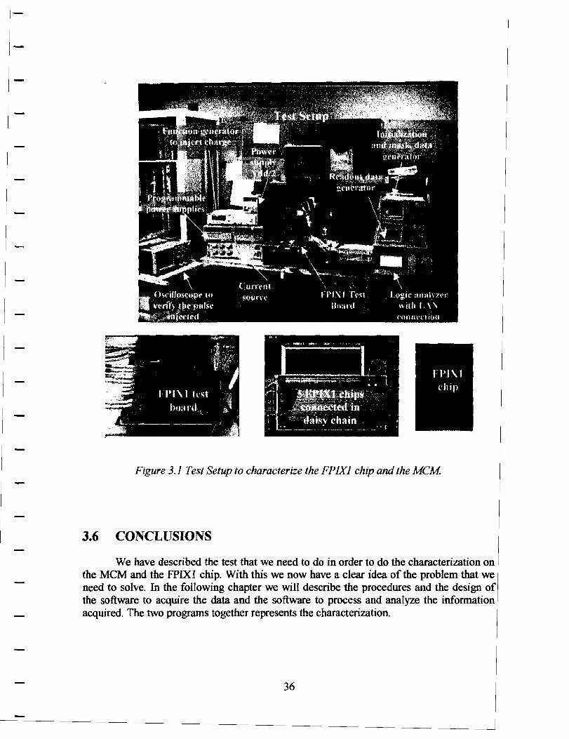
Figure 3.1 Test Setup to characterize the FPJXJ chip and the MCM
3.6 CONCLUSIONS
We have described the test that we need to do in order to do the characterization on the MCM and the FPIXI chip. With this we now have a clear idea of the problem that we need to solve. In the following chapter we will describe the procedures and the design of the software to acquire the data and the software to process and analyze the information acquired. The two programs together represents the characterization.
36
CHAPTER FOUR
SOFTWARE
The entire BTeV pixel detector will contain nearly 30 million pixel unit cells each bump-bonded to its associated front-end electronics cell. Since the total number of components is so large, they will not be tested at a single facility, but will be tested at three or four different collaborating institutions. For this reason, the test stand has been developed using test equipment that is commercially available and in common use. Also, the software has been developed utilizing the Laboratory Virtual Instrument Engineering Workbench (LabVIEW) [4], which is widely used among the collaboration and which is familiar to both physicists and engineers. LabVIEW is a development environment based on the graphical programming language G. It is integrated fully for communication with hardware such as GPIB, VX:l, PXI, RS-232, RS-485, and plug-in data acquisition boards by means of PCI interfaces. It also provides an extensive set of commands for file manipulation, including Ethernet transfers. This programming language is both very easy to understand and flexible. It also incorporates a number of sophisticated analysis techniques. We were thus able to develop the complex software needed for these tests entirely within this framework. The software has been designed to be very versatile, i.e., utilizing this software you can characterize the entire MCM or you can characterize a single FPIXl chip. In the following sections we will describe the design of the software.
37
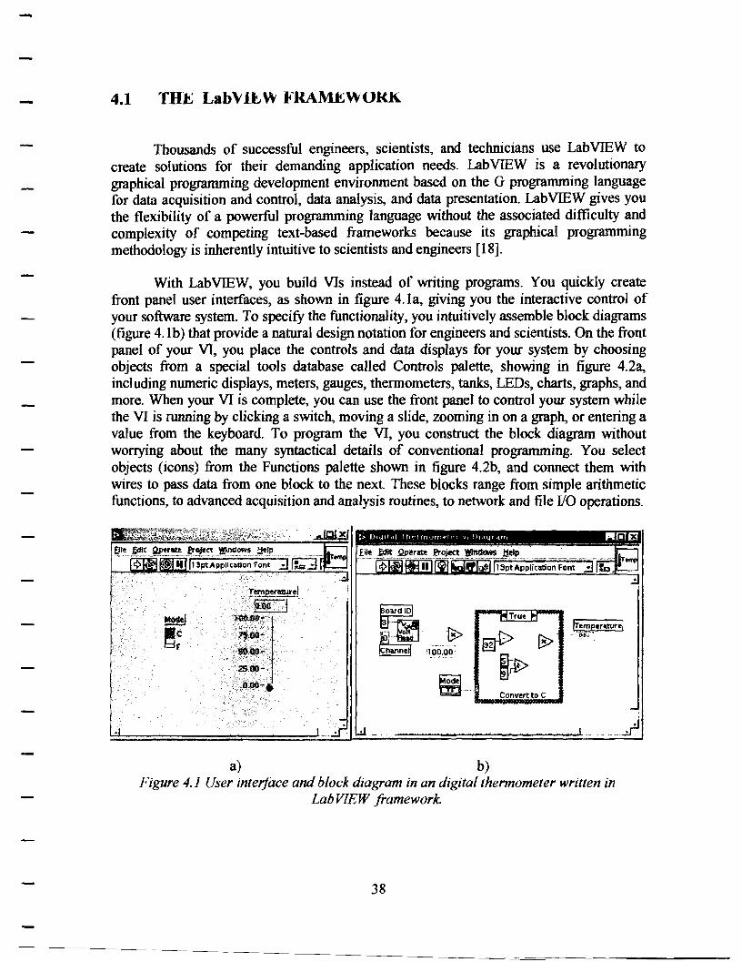
4.1 TH~ Lab\' Ji;W }'RA~WOKK
Thousands of successful engineers, scientists, and technicians use Lab VIEW to create solutions for their demanding application needs. LabVIEW is a revolutionary graphical programming development environment based on the G programming language for data acquisition and control, data analysis, and data presentation. LabVIEW gives you the flexibility of a powerful programming language without the associated difficulty and complexity of competing text-based frameworks because its graphical programming methodology is inherently intuitive to scientists and engineers [18].
With LabVIEW, you build Vis instead of writing programs. You quickly create front panel user interfaces, as shown in figure 4. la, giving you the interactive control of your software system. To specify the functionality, you intuitively assemble block diagrams (figure 4. lb) that provide a natural design notation for engineers and scientists. On the front panel of your VI, you place the controls and data displays for your system by choosing objects from a special tools database called Controls palette, showing in figure 4.2a, including numeric displays, meters, gauges, thermometers, tanks, LEDs, charts, graphs, and more. When your VI is complete, you can use the front panel to control your system while the VI is running by clicking a switch, moving a slide, zooming in on a graph, or entering a value from the keyboard. To program the VI, you construct the block diagram without worrying about the many syntactical details of conventional programming. You select objects (icons) from the Functions palette shown in figure 4.2b, and connect them with wires to pass data from one block to the next These blocks range from simple arithmetic functions, to advanced acquisition and analysis routines, to network and file 1/0 operations.
r-"'14 True H
a) b)
tfrm_~eruure/ --''l\&.t
Figure 4.1 User interface and block diagram in an digital thermometer written in Lab VIEW framework.
38
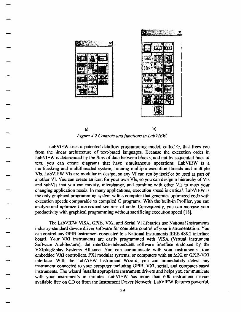
a) b)
Figure 4.2 Controls and functions in LabVJEW.
LabVIEW uses a patented dataflow programming model, called G, that frees you from the linear architecture of text-based languages. Because the execution order in Lab VIEW is determined by the flow of data between blocks, and not by sequential lines of text, you can create diagrams that have simultaneous operations. Lab VIEW is a multitasking and multithreaded system, running multiple execution threads and multiple VIs. Lab VIEW Vls are modular in design, so any VI can run by itself or be used as part of another VI. You can create an icon for your own Vls, so you can design a hierarchy of Vis and subVIs that you can modify, interchange, and combine with other Vis to meet your changing application needs. In many applications, execution speed is critical. Lab VIEW is the only graphical programming system with a compiler that generates optimized code with execution speeds comparable to compiled C programs. With the built-in Profiler, you can analyze and optimize time-critical sections of code. Consequently, you can increase your productivity with graphical programming without sacrificing execution speed [18].
The Lab VIEW VISA, GPIB, VXl, and Serial VI Libraries use National Instruments industry-standard device driver software for complete control of your instrumentation. You can control any GPIB instrument connected to a National Instruments IEEE 488.2 interface board. Your VXI instruments are easily programmed with VISA (Virtual Instrument Software Architecture), the interface-independent software interface endorsed by the VXIplug&play Systems Alliance. You can communicate with your instruments from embedded VXI controllers, PXI modular systems, or computers with an MXI or GPIB-VXI interface. With the LabVIEW Instrument Wizard, you can immediately detect any instrument connected to your computer including GPIB, VXI, serial, and computer-based instruments. The wizard installs appropriate instrument drivers and helps you communicate with your instruments in minutes. LabVIEW has more than 600 instrument drivers available free on CD or from the Instrument Driver Network. Lab VIEW features powerful,
39
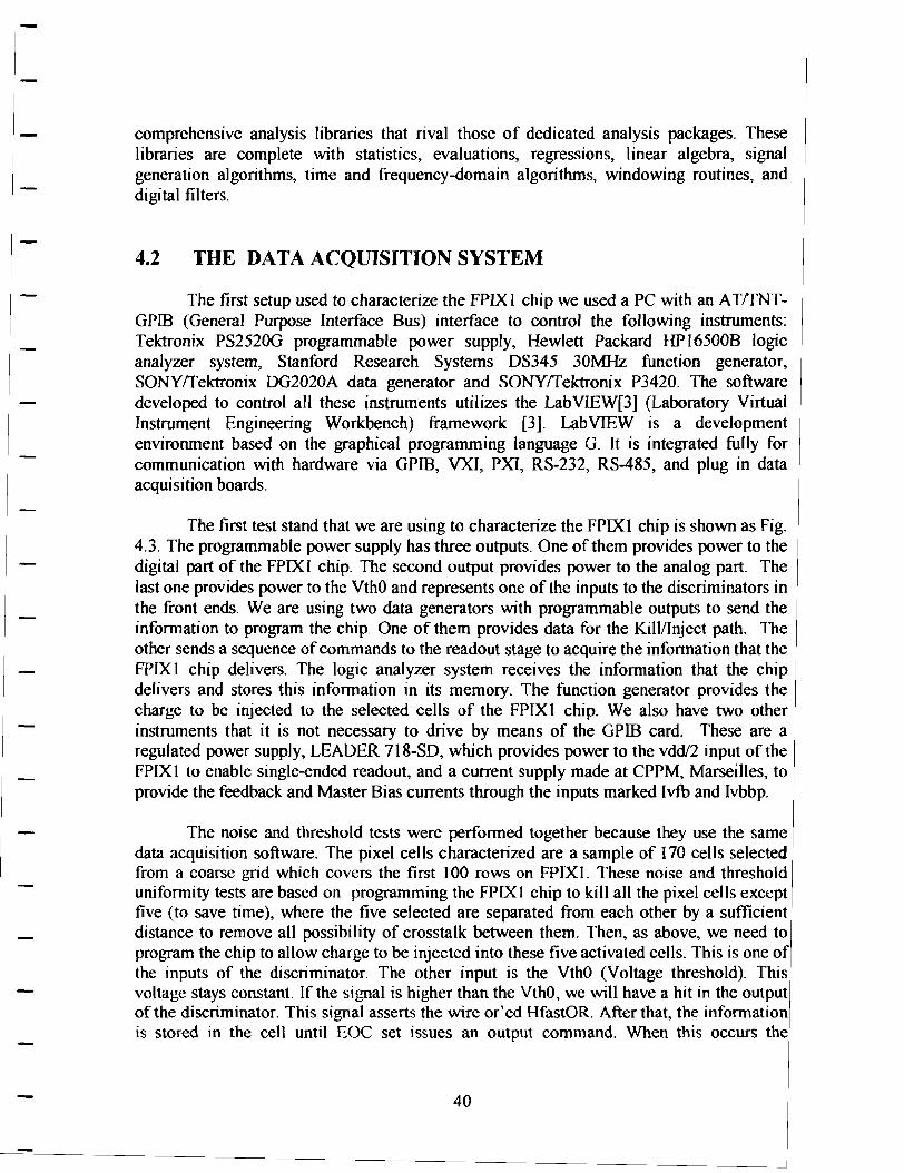
comprehensive analysis libraries that rival those of dedicated analysis packages. These libraries are complete with statistics, evaluations, regressions, linear algebra, signal generation algorithms, time and frequency-domain algorithms, windowing routines, and digital filters.
4.2 THE DATA ACQUISITION SYSTEM
The first setup used to characterize the FPIXl chip we used a PC with an ATffNTGPIB (General Purpose Interface Bus) interface to control the following instruments: Tektronix PS2520G programmable power supply, Hewlett Packard HP16500B logic analyzer system, Stanford Research Systems DS345 30MHz function generator, SONY!fektronix DG2020A data generator and SONY!fektronix P3420. The software developed to control all these instruments utilizes the LabVIEW[3] (Laboratory Virtual Instrument Engineering Workbench) framework [3]. LabVIEW is a development environment based on the graphical programming language G. It is integrated fully for communication with hardware via GPIB, VXI, PXI, RS-232, RS-485, and plug in data acquisition boards.
The first test stand that we are using to characterize the FPIXI chip is shown as Fig. 4.3. The programmable power supply has three outputs. One of them provides power to the digital part of the FPIX I chip. The second output provides power to the analog part. The last one provides power to the VthO and represents one of the inputs to the discriminators in the front ends. We are using two data generators with programmable outputs to send the information to program the chip. One of them provides data for the Kill/Inject path. The other sends a sequence of commands to the readout stage to acquire the information that the FPIX I chip delivers. The logic analyzer system receives the information that the chip delivers and stores this information in its memory. The function generator provides the charge to be injected to the selected cells of the FPIXl chip. We also have two other instruments that it is not necessary to drive by means of the GPIB card. These are a regulated power supply, LEADER 718-SD, which provides power to the vdd/2 input of the FPIX 1 to enable single-ended readout, and a current supply made at CPPM, Marseilles, to provide the feedback and Master Bias currents through the inputs marked Ivfb and Ivbbp.
The noise and threshold tests were performed together because they use the same data acquisition software. The pixel cells characterized are a sample of 170 cells selected from a coarse grid which covers the first 100 rows on FPTXI. These noise and threshold uniformity tests are based on programming the FPlXI chip to kill all the pixel cells except five (to save time), where the five selected are separated from each other by a sufficient distance to remove all possibility of crosstalk between them. Then, as above, we need to program the chip to allow charge to be injected into these five activated cells. This is one of the inputs of the discriminator. The other input is the VthO (Voltage threshold). This voltage stays constant. If the signal is higher than the VthO, we will have a hit in the output of the discriminator. This signal asserts the wire or'ed HfastOR. After that, the information is stored in the cell until EOC set issues an output command. When this occurs the
40
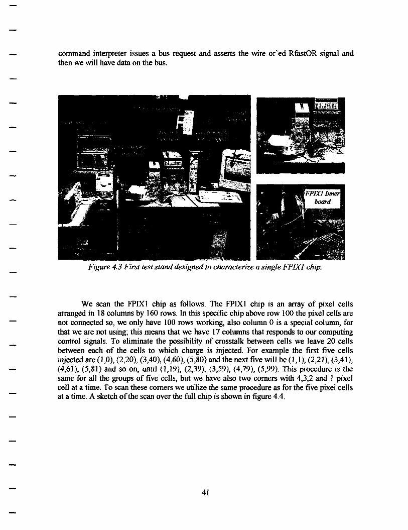
command interpreter issues a bus request and asserts the wire or' ed RfastOR signal and then we will have data on the bus.
Figure 4.3 First test stand designed to characterize a single FPIXI chip.
We scan the FPIXl chip as follows. The FPIXI chip is an array of pixel cells arranged in 18 columns by 160 rows. In this specific chip above row I 00 the pixel cells are not connected so, we only have I 00 rows working, also colwnn 0 is a special colwnn, for that we are not using~ this means that we have 17 columns that responds to our computing control signals. To eliminate the possibility of crosstalk between cells we leave 20 cells between each of the cells to which charge is injected. For example the first five cells injected are (1,0), (2,20), (3,40), (4,60), (5,80) and the next five will be (1,1), (2,21), (3,41), (4,61), (5,81) and so on, until (1,19), (2,39), (3,59), (4,79), (5,99). This procedure is the same for all the groups of five cells, but we have also two comers with 4,3,2 and 1 pixel cell at a time. To scan these comers we utilize the same procedure as for the five pixel cells at a time. A sketch of the scan over the full chip is shown in figure 4.4.
41
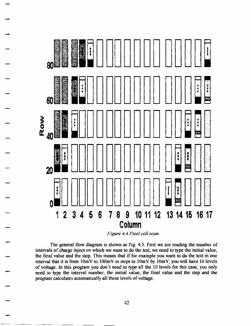
20
0 1 2 3 4 5 6 7 8 9 10 11 12 13 14 15 16 17
Column Figure 4.4 Pixel cell scan.
The general tlow diagram is shown as Fig. 4.5. First we are reading the number of intervals of charge inject on which we want to do the test, we need to type the initial value, the final value and the step. This means that if for example you want to do the test in one interval that it is from 1 Om V to 1 OOm V in steps to 1 Om V by 1 Om V, you will have 10 levels of voltage. In this program you don't need to type all the 10 levels for this case, you only need to type the interval number, the initial value, the final value and the step and the program calculates automatically all these levels of voltage.
42
The program has the particularity of accept more than one interval of voltages. With this we are obtained the number of levels on which the program will do the test, later on the program loads the initial kill/inject mask and readout patterns. Send to program the function generator with the current voltage. Send to clear the kill/inject patterns, this means that
. when you select the first five pixel cells and do the process, when you will select the next five pixel cells you need to disable the previous cells. With this clear we are disable these previous cells to enable the next five cells. With this we are getting the new group of five cells and we are sending to program the first data generator with the new group of cells. Send to put the logic analyzer in standby, initialize a counter. Send to program the second function generator to send the trigger to the function generator to tell him that it is time to send the inject charge, and also send the commands to do the readout. Save the data that the chip delivers in the internal memory of the logic analyzer. Ask if the counter is equal to 1000 if not come back and to again the full procedure, if yes the PC gets all the data from the logic analyzer.
The PC counts how many times is answering each cell of the group, save the result in a file, increment other counter. Ask if the counter is equal to 42, this means the 21 groups of cells, but how we are scanning the first two rows, this represent a total of 42 groups of cells. If the answer is no, come back and do the process until the answer is yes. Then ask if all the levels of voltage it was running if the answer is not, come back and do all the process with a new level of voltage. If the answer is yes, process all the data to get the errf(Vpp) for each pixel cell. Analyzes the data resulting to get the histogram and the gaussian for the voltage threshold and noise and ends.
The first subroutine is the process data to get the errf(Vpp) for each cell. The data processing software calculates the efficiency as a function of the voltage peak-peak by counting the number of hits (of 1000 possible) received. We then perform a least squares fit using the nonlinear Levenberg-Marquardt (Lev-Mar) fitting technique on the data for each cell to obtain the best threshold and noise value.
The second subroutine is the analysis to fill the histogram and perform the gaussian fit for the distributions for the 170 pixel cells, the program then performs a statistical analysis using the values from the 170 cells to get the means and standard deviations of the threshold and noise in units of electrons. At the end the program displays histograms of the noise and thresholds for the 170 cells along with the corresponding gaussian curve.
Both subroutines are shown in figures 4.5 and 4.6.
43
44
} 'igure 4. 6 Principal subroutines of the first software designed
45
To do the design the software we need to keep in mind the time response of the ·instruments to the commands sent to them by means of the GPIB interface. This times response are summarized in table 4.1
ln..rrument Operation lk..,pon..,l' ("l':.!) Initialization 60
kill/Inject Data generator masks
Readout 60 Acquisition 20 Transfer of 60
Logic analyzer data form the logic analyzer
Computer Count 30 Process 25200
Table 4. I Time response of the instruments
Then, the noise and threshold uniformity test was performed in approximately 85.4 hours, for that we need to do modifications on the first software designed to be able to reduce the time of running of the software.
The new software we have developed takes advantage of the very flexible environment provided by Lab VIEW as well as the advanced data analysis features it provides. While the use of LabVlEW and the relatively slow General Purpose Interface Bus (GPIB) for data acquisition meant that the tests were potentially time-consuming, several time-saving measures were taken that increased testing speed considerably. The test described in detail here is for the five chips on the MCM. The single chip test is the same, except for the masks.
First, two personal computers are employed, operating in parallel, both running LabVIEW programs under the Windows NT operating system. The first, PCI, is programmed for data acquisition. The second, PC2, performs the data analysis. The use of a logic analyzer with a Local Area Network (LAN) connection to receive the raw data and pass it on to PC2 makes it possible for the two computers to work simultaneously during the tests.
Second, two data generators are used to send commands to the chips and to the various instruments. This means that only small changes are needed on each cycle and thus a small amount of new information needs to be downloaded per data read cycle. Because of the many cycles involved, this results in a very large reduction in time. The data acquisition program running in PC 1 synchronizes the action of th~ two.
We have demonstrated that an adequate characterization of each chip, by which we mean measurements of discriminator threshold uniformity and electronic noise dispersion, can be achieved by charge injecting I 0% of the cells in a grid that covers the entire chip
46
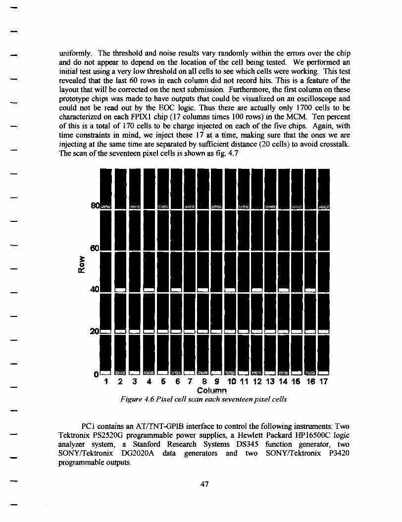
unifonnly. The threshold and noise results vary randomly within the errors over the chip and do not appear to depend on the location of the cell being tested. We pertonned an initial test using a very low threshold on all cells to see which cells were working. This test revealed that the last 60 rows in each column did not record hits. This is a feature of the layout that will be corrected on the next submission. Furthennore, the first column on these prototype chips was made to have outputs that could be visualized on an oscilloscope and could not be read out by the EOC logic. Thus there are actually only 1700 cells to be characterized on each FPIXl chip (17 columns times 100 rows) in the MCM. Ten percent of this is a total of 170 cells to be charge injected on each of the five chips. Again, with time constraints in mind, we inject these 17 at a time, making sure that the ones we are injecting at the same time are separated by sufficient distance (20 cells) to avoid crosstalk. The scan of the seventeen pixel cells is shown as fig. 4. 7
PCl contains an ATfTNT-GPIB interface to control the following instruments: Two Tektronix PS2520G programmable power supplies, a Hewlett Packard HP16500C logic analyzer system, a Stanford Research Systems DS345 function generator, two SONYffektronix DG2020A data generators and two SONYffektronix P3420 programmable outputs.
47
The test proceeds as follows: The program running in PCI first initializes all the instruments used in the test and sets them to their nominal values. The two programmable power supplies provide power to the digital part of the FPIXI chips, the analog part of the FPIXI chips, and to all five VthO tenninals of the chips on the module. These represent one of the inputs to the discriminators in the front ends. There are also two other instruments that are set manually. These are a regulated power supply, LEADER 718-SD, which provides power to the vdd/2 input of the FPIXl to enable single-ended readout, and a current supply made at CPPM, Marseilles, to provide the feedback and Master Bias currents.
PCl then initializes the five FPIXl chips using the first of the two data generators. First, it configures the chips in continuous mode, and, since we have several chips connected in daisy chain, it gives each of the chips a unique ID number (ChipID). The FPIXI chips deliver their infonnation in two words, the data word and the control word. The data word contains the ADC value, the column and the row~ the control word contains the ChipID number and the BCO number, which for these tests was always zero. PCl then programs the five FPIX 1 s to kill (disable) all the pixels cells except 17 by means of the first data generator. The data generator sends the infonnation to the chip in serial fonnat. To make this easier to do we decide to generate the input parameter from the number of the pixel cell in tenns of column and row. To do that we deduced a couple of equations that can do the translation of column and row into a serial number. As we discussed in chapter two there is a special scan path, for odd columns, the scan path starts in the lowest pixel and goes up to the highest pixel, and for even columns, the scan path starts in the highest pixel and goes down to the lowest pixel. Then the equation for an odd column is:
PC = ( OddCol * 160) + NumRow (4.1)
And for an even column the equation is:
PC= [(EvenCol +I)* 160]-1- NumRow (4.2)
Where: PC is the number of the pixel cell in the serial stream to be selected in the data generator, OddCol is the number of the odd column, EvenCol is the number of the even column, NumRow is the number of the row.
The same data generator is then used to enable charge injection to the 85 cells ( 17 times 5) it has selected. Next PCl sends commands to the logic analyzer to initialize it and to tell it to wait for a trigger that is based on bits in the data fonnat that the chips deliver. As we saw in chapter two there is a signal that the chip delivers called Data Valid. When you have a hit in the discriminator output this signal will be logic one (3.3V), and with the signal called Data 15 you can identify if the infonnation acquired is a control word or a data word. Then, the trigger that the logic analyzer is waiting for when at the same time a logic one is present in the signal Data Valid and a logic one is also present in the signal Data 15.
48
Following this, PC l uses the second data generator to send a trigger to the function generator DS345, which injects charge to each of the enabled cells. Any cell in which this charge produces a signal at the output of the second amplification stage that is greater than VthO will have a hit in the output of its discriminator. The cell then asserts the wire or'ed HfastOR and stores the hit information until the EOC set issues an output command. When this occurs the command interpreter issues a bus request, asserts the wire or'ed RfastOR signal, and presents its data on the bus.
The second data generator has also been programmed to send the commands to perform the read out of the FPIXl chips a fixed time after the charge is injected. Upon receipt of these commands, the FPIXls send the data generated in response to the injected charge pulses to the logic analyzer in the order in which the token passes through them. The logic analyzer acquires the information in binary format and transmits it by means of a LAN connection to the other computer (PC2), which processes the data. For each set of 85 pixel cells PC 1 repeats the injection of the same charge the times of charge injections that you want, e.g., 50 times or 500 times and does this for all the charge levels contained in a specific interval values of the charge it injects, for example in a specific test we had 60 different values of the charge. When all the levels of charge have been scanned, the program changes the selection of the pixel cells and repeats the whole procedure until all 170 pixel cells on each of the five FPIXl chips have been scanned.
The change of the pixel cells is done in an original and special way. First you select the pixel cells to which you will send a logic zero (OV) choosing the right location in the serial stream by means of equations 4.1 and 4.2, both in the kill mask in order to activate the pixel cells and after this in the inject mask in order to inject the pixel cells selected. Then when the program finishes scanning all the levels of voltage for the pixel cells selected you need to change the selection of pixel cells. To do that we send a command to put a logic one in only the places in the kill/inject mask that we selected before to be logic zero. After that we send the new group of pixel cells to be characterized. By doing in this way we save a lot of time because the other way to do it is to load a complete file to disable all the pixel cells and later on to send to program the new group of pixel cells. To load a file the data generator takes more or less 60 second to do it, and this represents a lot of time when repeated at every change in the choice of cells. The process we designed means that we do not need to load a file. We just send commands by means of the GPIB interface to disable the previous group of pixel cells and the data generator takes only milliseconds to do that.
The levels of charge must be chosen to bracket the voltage threshold. To do this we make a preliminary scan over the chip to determine the optimal range for the test. For each test we fix VthO at a particular value. The step size over which we are doing the scan is lmV. We have carried out these threshold uniformity and noise tests in four different regions of operation. For example for one of the regions we apply to the VthO terminal 2.05V and the levels of voltage will be 51 with a initial voltage of 130m V, and a final voltage of 180mV in steps on lmV. When you applied 130mV to the pixel cells you will not see any hit, and with 180 m V you will have 500 hits in each pixel cell selected (assuming you inject 500 times).
49
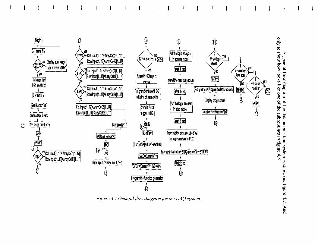
Vt 0
· Be~n I ·~ ,,__ __
Fet nBIM file/
f y!j
ln~alizethe · 61 andDG
Num ixels=1
u v
'
!Reset the KiMnject I
ut the logic anaty1er . in ac uire mode
' ~ait4sec)
' Program Shiftln Ylith DG1 : \'Ith the chosen eel~
~adoutpattem/ t
~ait 4 secJ : Progres tnt=Progres ~st+Numpixels
' . ' -• i Send a force :put the logic an~~er 101splay progres ast! 1 in stop mode ~
1 tri er to OG1 t 1 Numbeitile= umbeifile1 !
• ' ,(t_ !W=]] ~~· . ,----~
INumfilea~ 'Transmit the data acquired b • the logic analizerto PC2
!CurrentV=(ln~aN+W1000I 9
I i r,;;;-1File-nam-e=.,.,...Nam--=efi::-le+S1R1N=u-mb-e~-le~-S~-!
CVAC=Currentlf10] t '
ICYUC=(Curre~10Y2+0.01: !Wait ~sec.I
'P ii. fut . @ ! rogram u1e nction generator
' ij
~
Figure 4. 7 General flow diagram for the DA Q system.
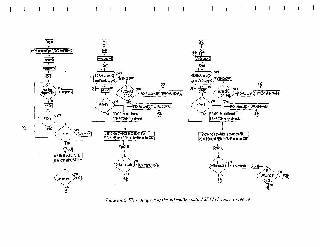
lx=(Numberch'1ps-1)'5770+5761+13 j
• Jimpar-OJ
I A1temaro=0J
' ~ t
-
'
~yes. ~-.J1mpar=1J
9no
I IK2f+11
\~
/Var4cop)"'(ll
~ ~A:xcol(Q) ~es I and Var4copy-O 1Var4~opya1 I
l~mno 1r yes 'I T Auxcol(Q) .. -~PC-=A-u-xc-ol(-Q)+-1.~160-·_,1.A,--ux-ro_w(,..,..,.Q) I ~R-2>0 L_~~~~~
no~~~~~~---,
PC• Auxcol(Q)"160+Auxrow(Q}
2R>Auxcol(Q) and Var4copy--O
~~· no 1(2 ~
I ino ,~es L_J ~ .. Alternal"1 et to low the bits in pos on ,
PB+1 PSI and PBl+1 of Shlftln in the DG1 •no
lniKillMask•!5770+13 lniln ectMask=J'5770+x
Figure 4.8 Flow diagram of the subroutine called 2FP!Xl conrtol reverse.
yes +-@]
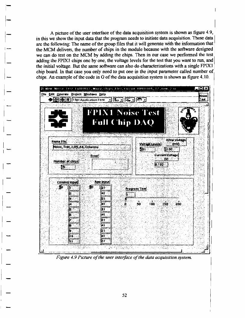
A picture of the user interface of the data acquisition system is shown as figure 4.9, in this we show the input data that the program needs to initiate data acquisition. These data are the following: The name of the group files that it will generate with the information that the MCM delivers, the number of chips in the module because with the software designed we can do test on the MCM by adding the chips. Then in our case we performed the test adding the FPIXI chips one by one, the voltage levels for the test that you want to run, and the initial voltage. But the same software can also do characterizations with a single FPIXI chip board. In that case you only need to put one in the input parameter called number of chips. An example of the code in G of the data acquisition system is shown as figure 4.10.
Figure 4.9 Picture of the user interface of the data acquisition system.
52
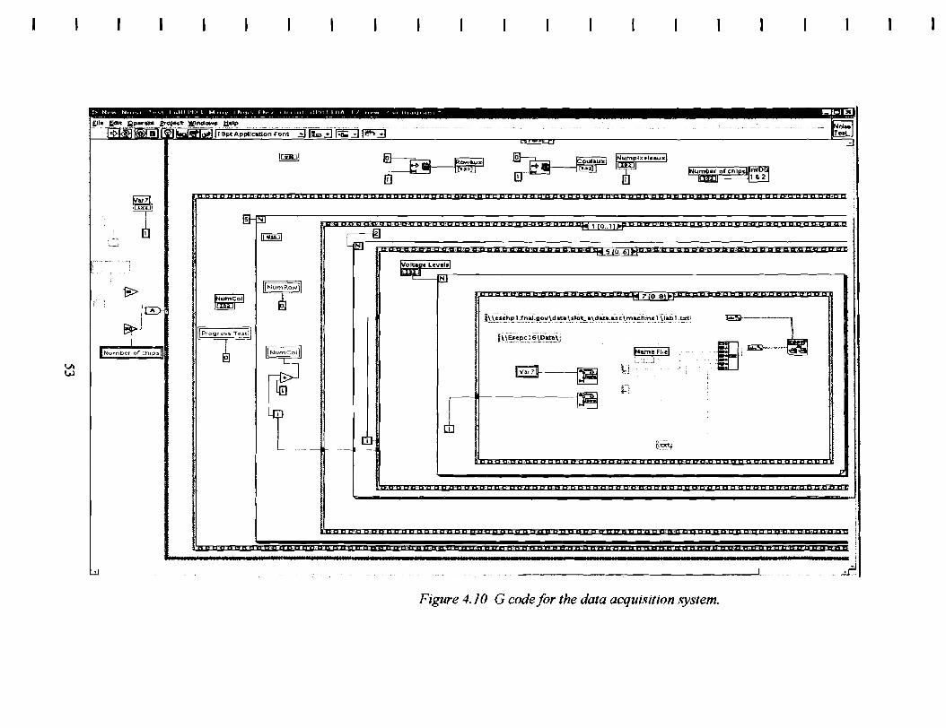
f 1sptApp11cat1on ront ::Jli,;:o!'.fl~ 318'i:::)
1 0 .. 1 i s
fNIDJ .------@ L~J N
5 0 .. 6
7 0 .. 8 ~. t&J;jo1I lfNu~Rm;fj]
I ,0 I j
'5··~~3 1§.;3 Number of ct-11ps
V'I ---c
w
Figure 4.10 G code for the data acquisition system.
4.3 DAT A ANALYSIS SYSTEM FERMILAB LIBRARY
PC2 processes the information collected to obtain the mean threshold with its corresponding standard deviation (threshold dispersion) and the mean noise with its corresponding standard deviation for each FPIXI chip on the MCM. When PCl begins to acquire data, PC2 waits until the transfer of information from the first 85 pixel cells finishes, which talces approximately 30 minutes. After this, both programs run at the same time. The data acquisition wait time is 3.5 minutes (adding an extra 5 minutes more to avoid any potential conflicts). The data processing program needs to wait for this time only once, because after the first transfer of data both programs can run simultaneously. The information processing takes exactly 30 minutes, so that the times are well matched. Thus, neither PC sits idle for an appreciable time during the test. While PC 1 is acquiring the data from the current 85 pixel cells, PC2 is processing the information from the previous 85 pixel cells.
Information processing proceeds as follows: First, PC2 translates the binary code that the data acquisition system has acquired into a file that contains the ChipID number, the column number, the row number, the count of hits recorded above threshold and the voltage at each step, as well as the count of total hits (charge injections). Then it calculates efficiency for each pixel cell by dividing the number of counts recorded over the total number of hits. The discriminator output in the front-end of the FPIXI chip is characterized by measuring its response as a function of the charge injected. Although only a single VthO is input to all 2880 cells on a chip, the value of the charge that triggers the discriminator may vary from cell to cell. This represents the threshold dispersion. The electrical charge injected can be calculated using the relationship between voltage and charge produced on the input capacitor. Since we have a capacitive load, C, of 6fF, the charge, Qinjecr, is
QinJecr = VppC = Vpp x 6x10-15 coulombs, (4.3)
where Vpp represents the voltage peak-peak delivered by the SRS DS345 function generator. The number of electrons that correspond to 1 m V can be obtained by means of the following relationship:
( VppC ) ( Vpp x 6 x 10 -
15 J (Q;,,icct )e = e- e = 1.6x10⁻¹⁹ e, (4.4)
with the result that
lmV---+ 31.5e. (4.5)
Because of the inherent noise of the electronics, the efficiency as a function of Vpp has the properties of an error function. For each pixel cell, a fit is performed to obtain the error function that best describes the experimental points. Lab VIEW has a library of
54
functions including one that performs a fit.using the nonlinear Levenberg-Marquardt (LevMar) method to determine a nonlinear set of coefficients which minimize chi-square [19]. First, PC2 plots the measured efficiency versus voltage Vpp (charge injected). The initial values of the threshold and noise are obtained using the data. The threshold value, Vthexp ,
is chosen to be the first value of the voltage that has greater than 50% hit efficiency. For the noise value, PC2 finds the first voltage for which the hit efficiency is greater than 81.5% and subtracts the value for 50% hit efficiency, which yields CT exp. These experimental
values are used as the initial guess coefficients for the nonlinear Lev-Mar Fit technique, since the fits will converge more quickly the closer the initial values are to the solutions. The nonlinear function needs to be specified, i.e., the relationship that describes the error function for each cell as a function of Vpp. For each point, Vpp, along the curve:
(4.6)
This technique provides two ways to calculate the Jacobian; i.e., the partial derivatives with respect to the coefficients, needed in the algorithm. These methods are: Numerical calculation: Uses a numerical approximation to compute the Jacobian. Formula calculation: Uses a formula to compute the Jacobian. For this one needs to specify the Jacobian functions, which are the partial derivatives of the error function with respect to CT and with respect to Vth. These functions are:
(
2 JV: {(V-Vth)2
] aerrf = (V -Vth) -a2 1 e 2a2 dV
aa .fi;a4 --00
(4.7)
Vpp {(V-Vth)2
]
iJerrf = (V -Vth) J e - 2a2 - dV iJ Vth J21i u 3
_00
(4.8)
The program repeats the above procedure for all of the pixel cells being tested. When the information for all the pixel cells has been analyzed, the results are output in five files, each of which contains the final information for all cells on one chip in the MCM, i.e., the column number, the row number, the best fit Vth in units of volts and electrons, and the best fit CT (noise) in units of volts and electrons. We then run a second program to histogram these quantities for the 170 cells on each of the five chips and to obtain the Gaussian curves that best fit these histograms for each file. We thus obtain the mean threshold, the sigma threshold (threshold dispersion), the mean noise and also the noise dispersion, all in units of volts and electrons for the 170 cells on each FPIXl chip. These results represent the characterization of the chips on the module.
55
'.Begin) •
Get Fllenamedata, filenameoutpu~ numberchips waittnltlal, waitprocess, vcltagelevels, initial voltage, Hits number
Ccl. lnpu~1 ... 17]'"ArrayCeC5[1. .. 17] ,__ _ ___, Rew In ut 1 ... 17 Arra eR51 ... 17
yes
----&.-'-~ ~ i I
Lead Filenamedata+STR{Var7)+STR{Q)
Hits counte
onvert the arrays Chip I , olumn-coun~
ow-count, counter and voltage count to preadsheet string and later store It In ilename_count_ +STR(Varn.DAT
Figure .:I. 7 General flow diagram for processing data system.
'no @
A picture of the user interface of the data analysis system is shown as figure 4.12, in this we can see how the user interface looks and the information that we need to run the program. This includes the name of the files that the data acquisition system is acquiring, the name of the file that will contain the results on each chip on the MCM, the time that the program needs to wait while PC 1 is acquiring the data, the time that the program needs to wait to begin to process the information acquired. Both these times need to be given in minutes. Also you need to provide to the program the voltage levels of the test that you are running, the initial voltage value in mV and the number of hits or injections with which you are doing the test. The group of seventeen pixel cells for which you are processing the information acquired by PCl appears in the window. As figure 4.13, we show the G code for the data processing system.
Figure 4. 12 Picture of the user interface for the data analysis system.
YI
.£JI<
'"" ... r~
I .J
Numbl"r of chips
~•l•v•t•I
IE2]11--+----
~~--E>.--19
~
310 .. lll
II Cc.lumr. inpwJ
Jeolumn CountJ.OW Count! I ~ lJ~ J:$:l) ~
lif ottage Co1.1m:I
Figure 4.13 G code for the data processing system.
.
We optimize the software described before, with all the modifications, we were able to reduce the running time of the system. We summarize all the time reductions in the following table 4.2
Tc.., t ~et up f n..,t ru llH.'111' \rqui,ition time and d:tta pron''' ( llottr..,)
I data generator, loading two files I logic analyzer (Transfer of the data by means
1 of the GPIB interface) 157.2 (One chip) 1 computer
2 data generators. One load the initialization 2 and the kill/Inject masks and the other load the
readout 118 (One chip) 1 logic analyzer (Transfer of the data by means
of the GPIB interface ) I computer
2 data generators .. One load the initialization 3 and the kill/Inject masks and the other load the
readout 85.4 (One chip) 1 logic analyzer (Transfer of the data by means
of the GPIB interface) 1 computer
2 data generators .. One load the initialization 4 and the kill/Inject masks and the other load the
readout 13.2 (Five chips) 1 logic analyzer (Transfer of the data by means
of a LAN) 1 computer
2 data generators .. One load the initialization 5 and the kill/Inject masks and the other load the
readout 6.2 (Five chips) 1 logic analyzer (Transfer of the data by means
of a LAN) 2 computers
Table 4.2 Test stand time optimization.
59
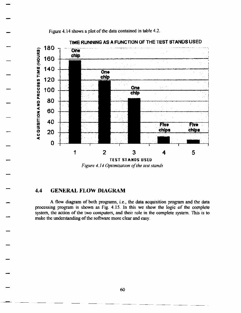
GI ~ ::> 0 :::c w :t -I-en en Ill u 0 O! IL Q z c z 0 -I--en 5 a u c
Figure 4.14 shows a plot of the data contained in table 4.2.
180
160
140
120
100
80
60
40
20
0
TIME RUNNING AS A FUNCTION OF THE TEST ST ANOS USED
1 2 3 4 TEST STANDS USED
Figure 4.14 Optimization of the test stands
5
4.4 GENERAL FLOW DIAGRAM
A flow diagram of both programs, i.e., the data acquisition program and the data processing program is shown as Fig. 4.15. In this we show the logic of the complete system, the action of the two computers, and their role in the complete system. This is to make the understanding of the software more clear and easy.
60
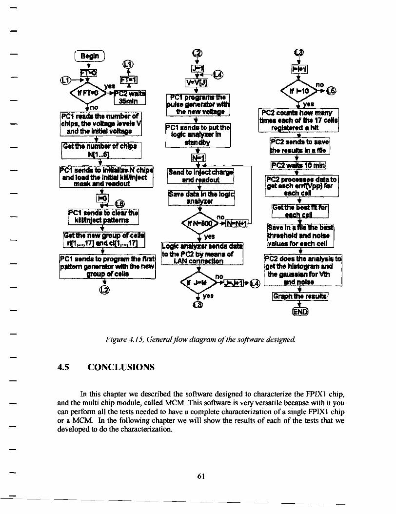
PC1 reads the numbtr of chips, the voltage levels
and th• inltilll voltqe
C1 sends to lnftldae N chip and load tht initial klllfnject
maak and readout
PC1 sends to program the ftflt pattern Qentretorwlth the new
group of ceu1
PC2 proce11 .. data to get each enft\'pp) for
Sne data In~ fosllc each ceH an er
Figure 4.15, <Jenera! flow diagram of the sojiware designed
4.5 CONCLUSIONS
In this chapter we described the software designed to characterize the FPIXl chip, and the multi chip module, called MCM. This software is very versatile because with it you can perform all the tests needed to have a complete characterization of a single FPIXl chip or a MCM. In the following chapter we will show the results of each of the tests that we developed to do the characterization.
61
CHAPTER FIVE
RESULTS OF THE CHARACTERIZATION
ln this chapter we will show all the results obtained from the characteriz.ation of the single FPIXI chip and for the MCM. We will see the results on the bad pixel map test, which we perfonned first for the single FPIX 1 chip to gain experience handling this type of chips. We will show the first results of the characteriz.ation on a single FPIXl chip and the setup that we used for that challenge. Once the multi chip module arrived at the laboratory to be characterized, we will describe how we added FPIXI chips one by one to it and the results of each chip. These test were performed without a sensor. We also describe the result of the MCM test with a sensor. Later on we will show the result of the reproducibility test and the hit test. These results represent the characterization of the FPIX 1 chip and the MCM.
5.1 BAD PIXEL MAP
We performed an initial test called the bad pixel map test, using a very low threshold on all cells to see which cells were working. This test revealed that the last 60 rows in each column did not record hits. This is a feature of the layout that will be corrected on the next submission. Furthermore, the first column on these prototype chips was made to have outputs that could be visualized on an oscilloscope and could not be read out by the EOC logic. A sketch of this result is shown in Fig. 5. 1.
62
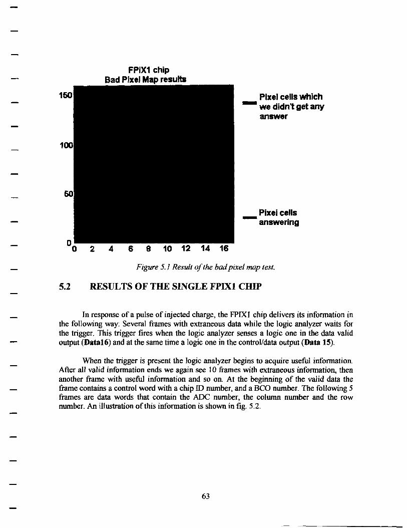
150
2
FPIX1 chip Bad Pixel Map results
4 6 8 10 12 14 16
Pixel cells which - we didn't get any
answer
Pixel cells - answering
Figure 5.1 Result of the bad pixel map test.
5.2 RESULTS OF THE SINGLE FPIXl CHIP
In response of a pulse of injected charge, the FPIXI chip delivers its infonnation in the following way: Several frames with extraneous data while the logic analyzer waits for the trigger. This trigger fires when the logic analyzer senses a logic one in the data valid output (Data16) and at the same time a logic one in the control/data output (Data 15).
When the trigger is present the logic analyzer begins to acquire useful information. After all valid information ends we again see 10 frames with extraneous informatio~ then another frame with useful information and so on. At the beginning of the valid data the frame contains a control word with a chip ID number, and a BCO number. The following 5 frames are data words that contain the ADC number, the column number and the row number. An illustration of this information is shown in fig. 5.2.
63
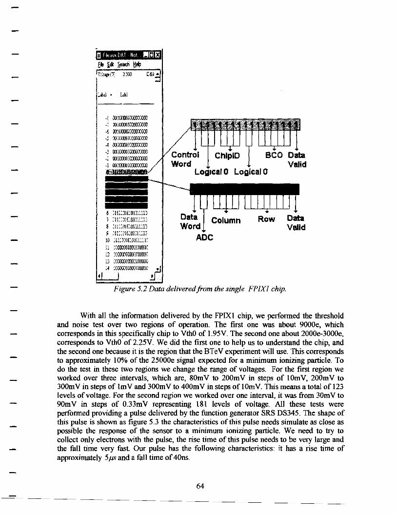
:.rmi • W.l
-? OOJWllJC{(O)G((IJ . ; cmcoonm:ooccro .t OOJCCOODC®JC(OO .5 OOJCCOOJCCOOJC-0:0 ...-. t\J1U:OOXOCOXWJ
t m::ow101mm 7 ::IDJ!OlOlJll3D 8 JlilJ.J!GlOIDLDJ 9 JIGJW:OIJU:lJ 1c1 m:rnc:om:m l l :CWJJC«OOCCOOX l2 }({(02,((0}J{((O)U
13 :cCCOJtroJ~,~CCOOu
i .i ~m:oxcroxlCror ..:.f.
• .!.I '
Data Column Word
Row Data Valid
ADC
Figure 5.2 Data delivered from the single FPJXJ chip.
With all the information delivered by the FPIXl chip, we performed the threshold and noise test over two regions of operation. The first one was about 9000e, which corresponds in this specifically chip to VthO of 1.95V. The second one about 2000e-3000e, corresponds to VthO of 2.25V. We did the first one to help us to understand the chip, and the second one because it is the region that the BTeV experiment will use. This corresponds to approximately 10% of the 25000e signal expected for a minimum ionizing particle. To do the test in these two regions we change the range of voltages. For the first region we worked over three intervals, which are, 80m V to 200m V in steps of 1 Om V, 200m V to 300mV in steps of lmVand 300mV to 400mV in steps of IOmV. This means a total of 123 levels of voltage. For the second region we worked over one interval, it was from 30m V to 90mV in steps of 0.33mV representing 181 levels of voltage. All these tests were performed providing a pulse delivered by the function generator SRS DS345. The shape of this pulse is shown as figure 5.3 the characteristics of this pulse needs simulate as close as possible the response of the sensor to a minimum ionizing particle. We need to try to collect only electrons with the pulse, the rise time of this pulse needs to be very large and the fall time very fast. Our pulse has the following characteristics: it has a rise time of approximately 5 µs and a fall time of 40ns.
64
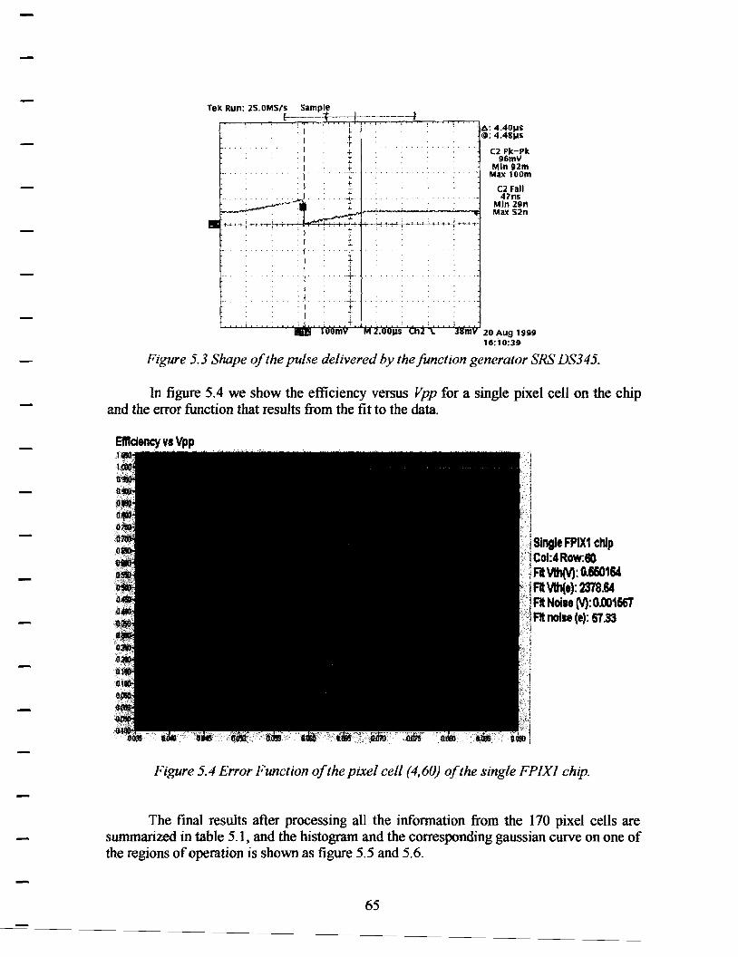
Tek Run: 25.0MS/s sample l-·----- --- -----·-·-·--1
''. '. : I . . I +
. : 1 · t . I ±
·I ... L .. , . l.
: I >· ± : J. . ... ...;_ ...
• I : I
1 : I . I . I . I . I : ., . I
. 4-...... ~ ... ± l.
.... ·{-· .
a: 4.40µs !IP: 4.48µs
C2 Pit-Pk 96mV
Min 92m Max lOOm
C2 Fall 47ns
Min 29n Max S2n
m 20 Aug 1999 1Cl:iO:J9
Figure 5. 3 Shape of the pulse delivered by the function generator SRS DS345.
In figure 5.4 we show the efficiency versus Vpp for a single pixel cell on the chip and the error function that results from the fit to the data.
Emdency vs Vpp .MIO... . . tjf
Single FPIX1 chip Col:4 Row:GO Fit\llh(V): 0.660164 FIW1(e): 2378.64 Flt Noise M: 0.001667 Flt noise (e): 6T .33
Figure 5.4 Error Function of the pixel cell (4,60) of the single FP/Xl chip.
The final results after processing all the infonnation from the 170 pixel cells are summarized in table 5.1, and the histogram and the corresponding gaussian curve on one of the regions of operation is shown as figure 5.5 and 5.6.
65
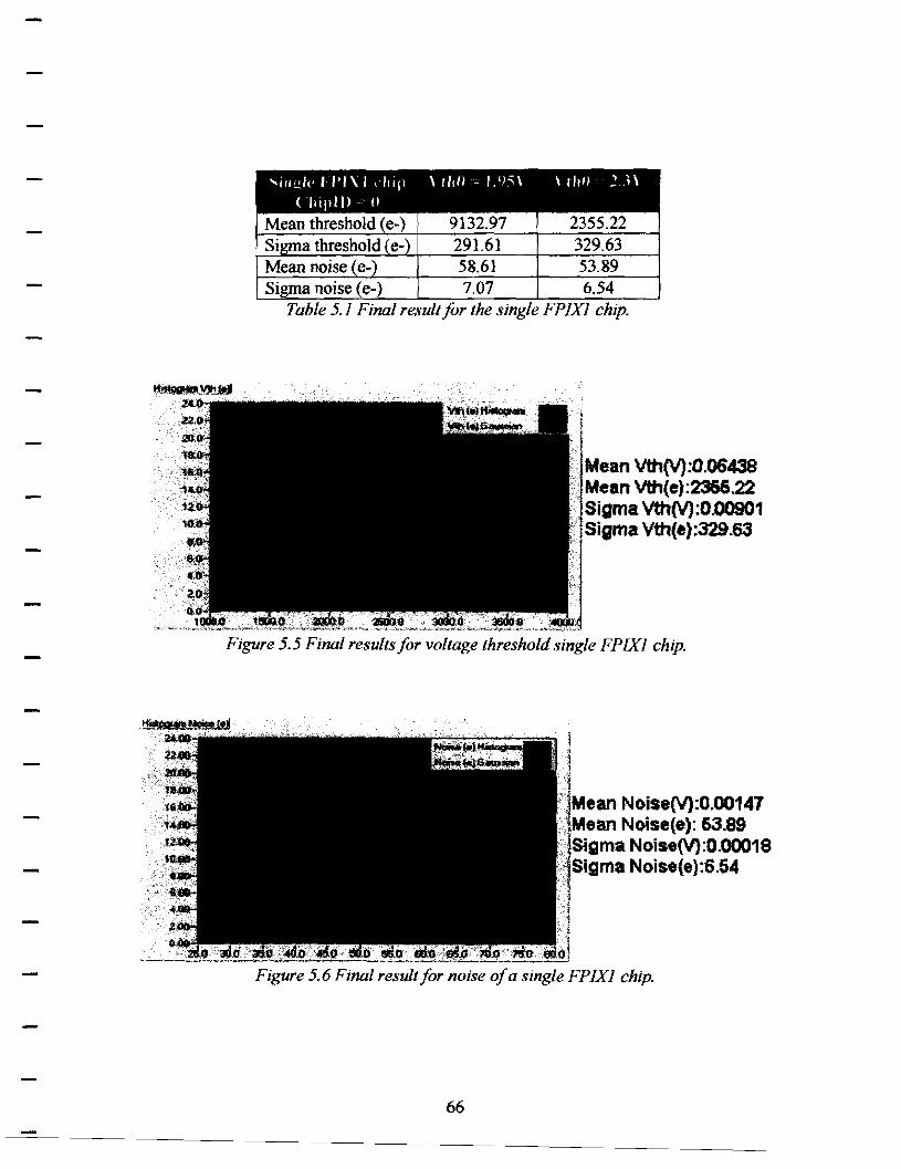
9132.97 291.61
Si a noise (e-) 7.07 6.54 Table 5.1 Final result for the single FPJXI chip.
Mean VthM:0.06438 Mean vth(e) :2366.22 Sigma VthM:O.oo901
· Sigma vth{e):329.63
Figure 5.5 Final results for voltage threshold single FPIXI chip.
{\Mean NoiseM:0.00147 ::;·Mean Noise{e): 63.89 .·Sigma NoiseM:0.00018
,<11Sigma Noise{e):6.54
,J .•• i · ... i
.~~~~'-==~~"""-~'-=~~~~·15h~':lli'lo1 Figure 5.6 Final result for noise of a single FPJXJ chip.
66
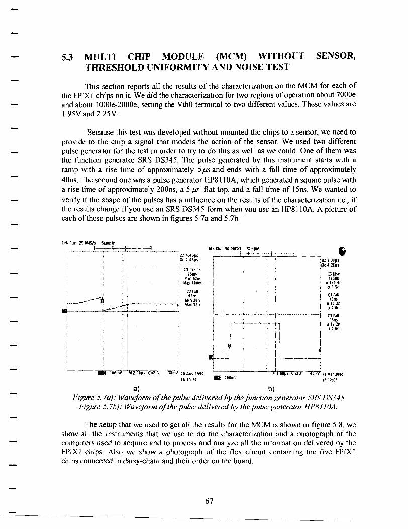
5.3 MULTI CHIP MODULE (MCM) WITHOUT SENSOR, THRESHOLD UNIFORMITY AND NOISE TEST
This section reports all the results of the characterization on the MCM for each of the FPIXI chips on it. We did the characterization for two regions of operation about 7000e and about IOOOe-2000e, setting the VthO terminal to two different values. These values are l.95V and 2.25V.
Because this test was developed without mounted the chips to a sensor, we need to provide to the chip a signal that models the action of the sensor. We used two different pulse generator for the test in order to try to do this as well as we could. One of them was the function generator SRS DS345. The pulse generated by this instrument starts with a ramp with a rise time of approximately 5 µs and ends with a fall time of approximately 40ns. The second one was a pulse generator HP8 l I OA, which generated a square pulse with a rise time of approximately 200ns, a 5 µr; flat top, and a fall time of I 5ns. We wanted to verify if the shape of the pulses has a influence on the results of the characterization i.e., if the results change if you use an SRS DS345 form when you use an HP81 IOA. A picture of each of these pulses are shown in figures 5.7a and 5.7b.
Tek Run: 25.0MSls Sample 1---+--·--+-·-·-·······--l
IA: 4.40µs J~: 4_4gµs
~ C2 Pk-Pk j 96mY : Min 92m 1 Max IOOm
C2 Fall 47ns
Min 29n Max 51n
--+--+--<--"~ ... ..._._ ...... ~~~ ' ' ;
' +
I .,
' I I
TmV 20 Aug 1999 16: 10:39
Tek Run 50 OMS/j ~a~ple _ ! ··---------l~~-~ •
~ A:J.OOµs
. ; I -- -·: ·- ---··· '.--~ .. ;-.. ·i .,_ .. [ , .. ·---· .... --·.' ·---·
i~1 ~ : : I , ~ I ·~~~~~
!Ji: 4.2Sµs
CJ Rise 19Sns
µ 19Mn C1 l.Sn
O fall tsns
µ to.in er 6. 6n
CJ Fall ISns
µIUn a 6.6n
8l IOOmY m 12 Mu 200G
17: 12:06
a) b) Figure 5. ?a): Waveform of the pulse delivered by the function generator SR.."i DS345
Figure 5. 7h): Waveform of the pulse delivered by the pulse generator HPBl IOA.
The setup that we used to get all the results for the MCM is shown in figure 5.8, we show all the instruments that we use to do the characterization and a photograph of the computers used to acquire and to process and analyze all the information delivered by the FPIX I chips. Also we show a photob>raph of the flex circuit containing the five FPIX 1 chips connected in daisy-chain and their order on the board.
67
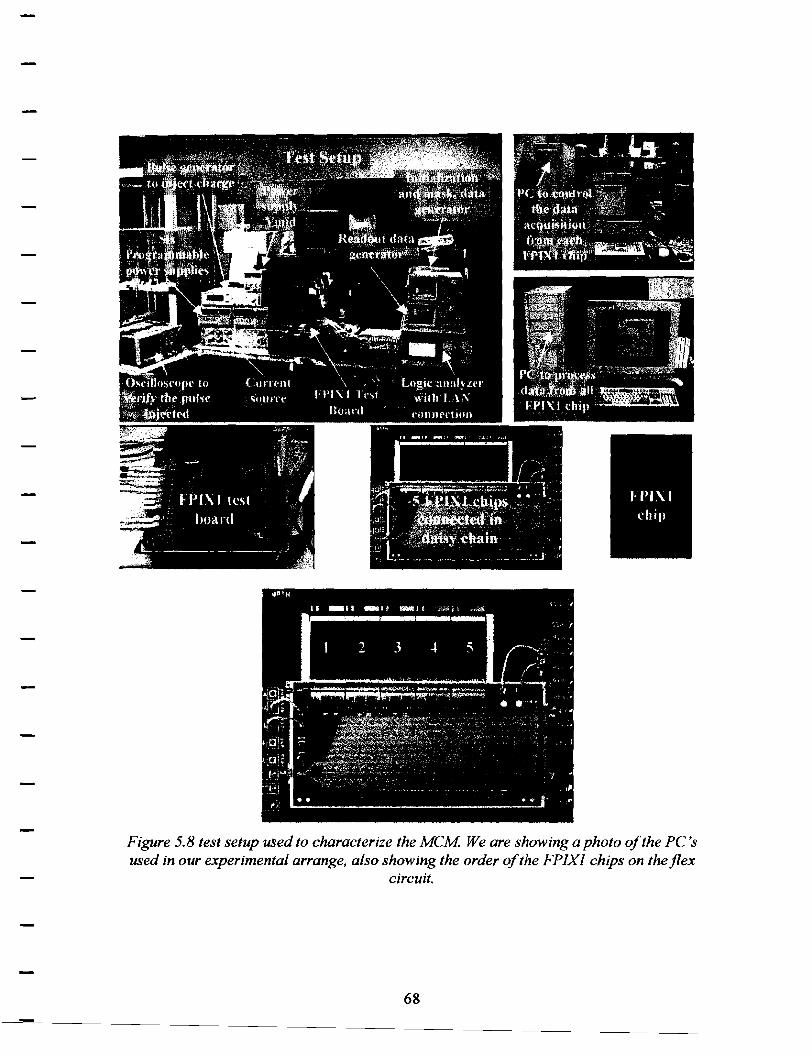
Figure 5.8 test setup used to characterize the MCM We are showing a photo of the PC's used in our experimental arrange, also showing the order of the FPIXJ chips on the flex
circuit.
68
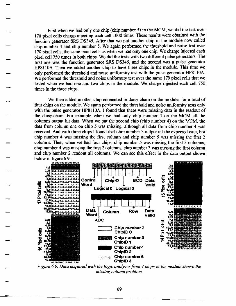
First when we had only one chip (chip number 5) in the MCM, we did the test over 170 pixel cells charge injecting each cell 1000 times. These results were obtained with the function generator SRS DS345. After that we put another chip in the module now called chip number 4 and chip number 5. We again performed the threshold and noise test over 170 pixel cells, the same pixel cells as when we had only one chip. We charge injected each pixel cell 750 times in both chips. We did the tests with two different pulse generators. The first one was the function generator SRS DS345, and the second was a pulse generator HP8110A. Then we added another chip to have three chips in the module. This time we only performed the threshold and noise uniformity test with the pulse generator HP811 OA. We performed the threshold and noise uniformity test over the same 170 pixel cells that we tested when we had one and two chips in the module. We charge injected each cell 750 times in the three chips.
We then added another chip connected in daisy chain on the module, for a total of four chips on the module. We again performed the threshold and noise uniformity tests only with the pulse generator HP811 OA. I found that there were missing data in the readout of the daisy-chain. For example when we had only chip number 5 on the MCM all the columns output hit data. When we put the second chip (chip number 4) on the MCM, the data from column one on chip 5 was missing, although all data from chip number 4 was received. And with three chips I found that chip number 3 output all the expected data, but chip number 4 was missing the first column and chip number 5 was missing the first 2 columns. Then, when we had four chips, chip number 5 was missing the first 3 columns, chip number 4 was missing the first 2 columns, chip number 3 was missing the first column and chip number 2 readout all columns. We can see this effect in the data output shown below in figure 6.9.
00000000000000000
1,8 2,21 OJ...ll.J...10.U.J.J.Ol.OJ...ll.
3,1 l.l.l.J.l.OOl.J.J.l..U.l.l.l. 4,20 o UJ.l.0 UUJ.O l.O ll.l. 5.o ouiJ.O iouiiuiu Control
.!! 5.28 Olll.l.OOl.l.J.l.Ol.Ol.J...l • 1,0 uJ.J.Oooi.uiul.J...l Word u 1,21 ouioJ.uUJ.ol.oiu Logical O Logical 0
- 9,0 l.l.l.Ol.l.Ol.lll.lll.U • 11,20 Ol.l.l.Ol.Ol.l..UOJ.Ol.J.J. _!! 11,0 Olll.Ol.OOJ.l.l.l.l.l.l.J...l ~ 12,21 OJ.UDO .l.ll.l.l.O.l.8l.l.l. ....... 13,. OlllOO l.Ollll.J.l.lll. - 14,21 Ul.OQOl.J.J.,l.Ol.Ol.ll
Ill =
15,1 l.l.l.00 00 l.lll.lll.l.l. 1S,2t .U.01.l.l.lll.l.Ol.Ol.l.l.
17,1 OUOl.l Ol..LJ.lll.l.l. 01.00.LO .1.0l.lllll.l.l.O
Data Column Word
Row
ADC
Chip number 2 ChlplDO
111•1 Chip number 3 ChiplD 1 Chip number4 ChiplD 2 Chip number 6 ChiplD 3
Data Valid
Figure 6.9. Data acquired with the logic analyzer from 4 chips in the module shown the missing column problem.
69
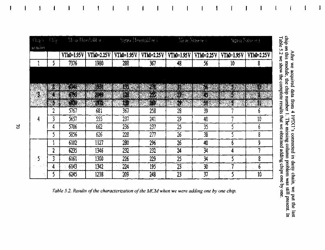
.....:i 0
4
5
2 5767 681 367 258 28 39 7 3 5657 555 237 241 29 40 7 4 5706 662 236 237 25 35 5 5 5856 626 228 277 26 38 5 1 6102 1127 280 296 26 40 6 2 6235 1346 232 232 24 34 4 3 6161 1300 226 229 25 34 5 4 ~143 1342 224 195 23 30 7 5 6245 1238 209 248 23 37 5
Table 5.2. Results of the characterization of the MCM when we were adding one by one chip.
6 10 6 8 9 7 8 6 10
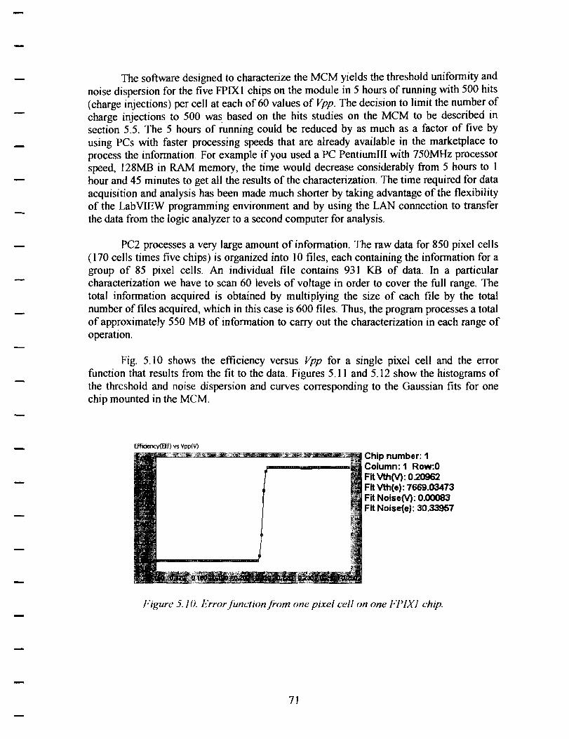
The software designed to characterize the MCM yields the threshold uniformity and noise dispersion for the five FPIX 1 chips on the module in 5 hours of running with 500 hits (charge injections) per cell at each of 60 values of Vpp. The decision to limit the number of charge injections to 500 wa~ based on the hits studies on the MCM to be described in section 5.5. The 5 hours of running could be reduced by as much as a factor of five by using PCs with faster processing speeds that are already available in the marketplace to process the information. For example if you used a PC PentiumIII with 750MHz processor speed, 128MB in RAM memory, the time would decrease considerably from 5 hours to 1 hour and 45 minutes to get all the results of the characterization. The time required for data acquisition and analysis has been made much shorter by taking advantage of the flexibility of the Lab VIEW programming environment and by using the LAN connection to transfer the data from the logic analyzer to a second computer for analysis.
PC2 processes a very large amount of information. The raw data for 850 pixel cells ( 170 cells times five chips) is organized into 10 files, each containing the information for a group of 85 pixel cells. An individual file contains 931 KB of data. In a particular characterization we have to scan 60 levels of voltage in order to cover the fu]) range. The total information acquired is obtained by multiplying the size of each file by the total number of files acquired, which in this case is 600 files. Thus, the program processes a total of approximately 550 MB of information to carry out the characterization in each range of operation.
Fig. 5.10 shows the efficiency versus Vpp for a single pixel cell and the error function that results from the fit to the data. Figures 5.11 and 5.12 show the histograms of the threshold and noise dispersion and curves corresponding to the Gaussian fits for one chip mounted in the MCM.
Efficiency(Eff) vs Vpp(V)
Chip number: 1 Column: 1 Row:O Flt Wl(V): 0.20962 Flt vth(e): 7669.03473 Fit Noise(V): 0.00083 Fit Noise(e): 30.33957
Figure 5.10. E"rrorfunctionfrom one pixel cell on one FPIXJ chip.
71
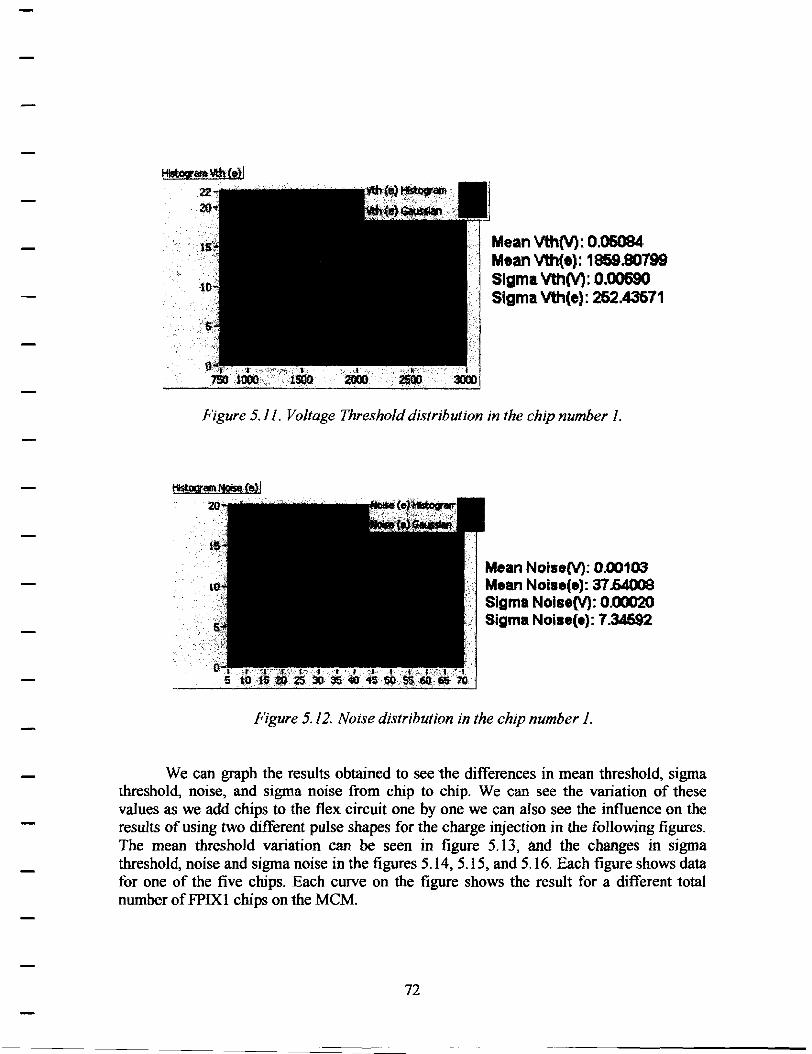
Mean vthM: O.~. Mean vth(e): 1859.80799 Sigma VthM: 0.00690 Sigma vth(e): 262.43671
Figure 5.11. Voltage Threshold distribution in the chip number I.
Mean NoiseM: 0.00103 Mean Noiae(e): 37 54008 Sigma NolseM: O.Q0020 Sigma Noise(e): 7.34592
Figure 5. I 2. Noise distribution in the chip number 1.
We can graph the results obtained to see the differences in mean threshold, sigma threshold, noise, and sigma noise from chip to chip. We can see the variation of these values as we add chips to the flex circuit one by one we can also see the influence on the results of using two different pulse shapes for the charge injection in the following figures. The mean threshold variation can be seen in figure 5.13, and the changes in sigma threshold, noise and sigma noise in the figures 5.14, 5.15, and 5.16. Each figure shows data for one of the five chips. Each curve on the figure shows the result for a different total number of FPIXl chips on the MCM.
72
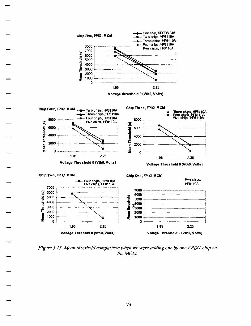
Chip Five, FPIX1 MCM -+-One chip, SRSDS 345 ----- Two chips, l-Rl110A -.....- Three chips, l-Rl110A
8000
~ 7000
::s! 6000 0 5000 .c
-+-Four chips, l-Rl110A FIVe chips, tff110A
Ill 4000 I!? .c 3000 I-c 2000 19
1000 GI :e
0 1.95 2.25
Voltage threshold 0 (VthO, Volts)
Chip Four, FPIX1 MCM ---Two chips, l-Rl110A -11- Three chips, l-Rl11 OA
8000 __ --··- __._ Four chips, l-Rl11 OA ~ FIVe chips, tff110A
__,,,,.~-------~; i:i 6000 0 .c Ill 4000 I!?
__ I
.c I- 2000 c 19
:I 0 1.95 2.25
Voltage Threshold 0 (VthO, Volts)
Chip Two, FPIX1 MCM
7000
~ 6000 ::s! 5000 0 .c 4000 Ill I!? 3000 .c I- 2000 c 19 1000 GI :E 0
__._Four chips, l-Rl110A F1Vechips, l-Rl110A
-·-··- ·-····-····--·- ····-- ··- ·-·······-·······--·-·····-··-·---1
~ '
~--------i i
1.95 2.25
Voltage Thrshold 0 (VthO, Volts)
Chip Three, FPIX1 MCM -11-Three chips l-Rl110A --.-. Four chips, 1-ff 11 OA
Rve chips, l-Rl110A 8000
~ ::s! 6000 0 .c Ill 4000 I!? .c I-
2000 c 19 GI :e 0
1.95 2.25
Voltage Threshold 0 (VthO, Volts)
Chip One, FPIX1 MCM
::s!
F1Vechips, l-Rl110A
~~~ -·---··--=-----·-·----------···---J _g 5000 +--------------~! = _4000 +--------------i .S .!sooo +------~--------i c 2000 +-----------------! i 1000 +------------ l
0+-------,.----------i 1.95 2.25
Volage Threshold 0 (VthO, Volts)
Figure 5.13. Mean threshold comparison when we were adding one by one FP !XI chip on theMCM
73
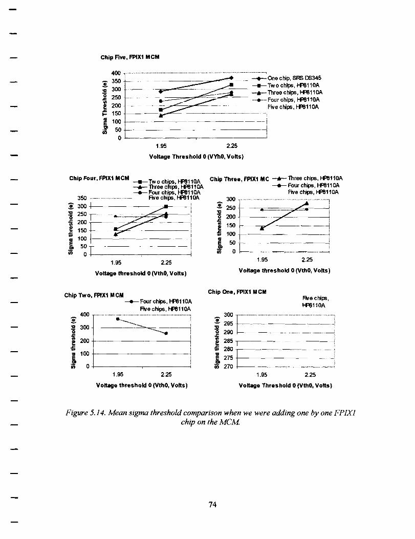
Chip Five, FPIX1 M CM
400
... 350 :; 300 :g 250
~ 200 ~ 150 +----~--=--- ---~ 100+--------.91 50 +------------· Cl)
1.95 2.25
Voltage Threshold 0 (VYhO, Volts)
Chip Four, FPIX1 M CM -+-Tw 0 ch' ' l-F811 OA -.-Three c~ps, l-F8110A -.-Four chips, l-F8110A
Five chips, l-F8110A 350 :i 300 +---------~--_,,jl--------<
~ 250-r------.__~-=-===;7'~~~:::;;;:;2.-----i .s::. 200+---- ~ ~ 150 ~ -
~ 100 i .91 50 +---·-------------; Cl) 0+-------~----------1
1.95 2.25
Voltage threshold 0 (VthO, Volts)
Chip Two, FPIX1 MCM ---.-Four chips, l-F8110A
Five chips, l-F8110A ••-• - ... ,_._,~~-•V·----~·-•v·-·••-•"-••~,~-·,-·-----·---·~-., - 400
.!!.. ~ 300+----~-~------------=~-----j· 0 ----..... ~ 200 +--------------i
= !! 100 +--------------------i C I
.91 ! Cl) 0+-------..---------;
1.95 2.25
Voltage threshold O (VthO, Volts)
Chip Three, FPIX1 MC _.,_Three chips, l-F8110A ---- Four chips, l-F8110A
Ave Chips, l-F8110A 300 -r··-· ............................... -- _______ ,, .............. -.----,
:i 250t------.~~====~~=-----1 ~
0 200 +------------------< .s::. ~ 150 +------.~-----------! = 100 +---------------; ~ 50~--~~~~~~
' 0 +-------.,...-------; 1.95 2.25
Voltage threshold 0 (VthO, Volts)
Chip One, FPIX1 MCM Five chips, 1-F8110A
- 300 ---··-------------·····--·---.--------------·----·---.. ~ .!!.. 295_,__ ____________ J ~
0 290 +----------------< .s::. ~ 285 +---------------____, = 280 +--------------1
~ 275 +-----------------1 ' 270 i
1.95 2.25
Voltage Threshold 0 (VthO, Volts)
Figure 5.14. Mean sigma threshold comparison when we were adding one by one FP !XI chip on the MCM
74
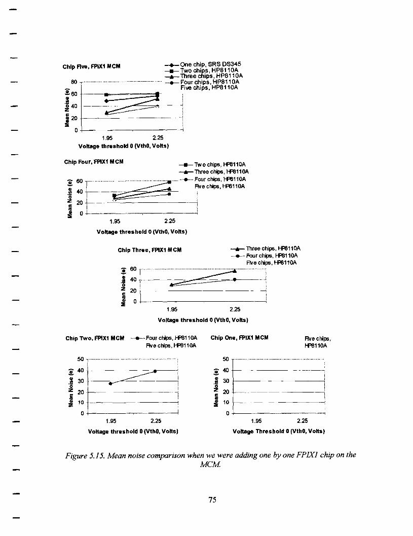
Chip Five, FPIX1 MCM -+-One chip, SRS 08345 ----- Two chips, HP8110A -11- Three chips, HP8110A
80 · --·· ·-----·---· .............. _ ·--····· ---- Four chips, HPB 11 OA Fiw chips, HP8110A
1.95 2.25
Voltage threshold 0 (VthO, Volts)
Chip Four, FPIX1 MCM ----- Two chips, tff11 OA -11-Threechips, tff110A i: ~- ~+r~= .. =,,,,:
i ot I I
1.95 2.25
Voltage threshold 0 (VthO, Volts)
Chip Three, FPIX1 MCM -11-Three chips, HF6110A ---- Four chips, tff110A
Five chips, HF6110A
1~r--~--1 :ll
1.95 2.25
Voltage threshold 0 (VthO, Volts)
Chip Two, FPIX1 MCM _._Four chips, tff110A Five chips, tff110A
Chip One, FPIX1 MCM Rvechips, tff110A
50 ····--··--···----·-···-·-·····----·--·-···---·----" !
~ 40
·I 30 z 20 +----· ---c i 10+-~~~~-~~~~
0+--------------< 1.95 2.25
Voltage threshold 0 (VthO, Volts)
~ 40 .,__ _______ --~
GI 30 +----- ----------.!!! 0
z 20+-------------' ; i :I 10 -\------------------!
O+-----------~
1.95 2.25
Voltage Threshold O (VthO, Volts)
Figure 5.15. Mean noise comparison when we were adding one by one FPJXJ chip on the MCM
75
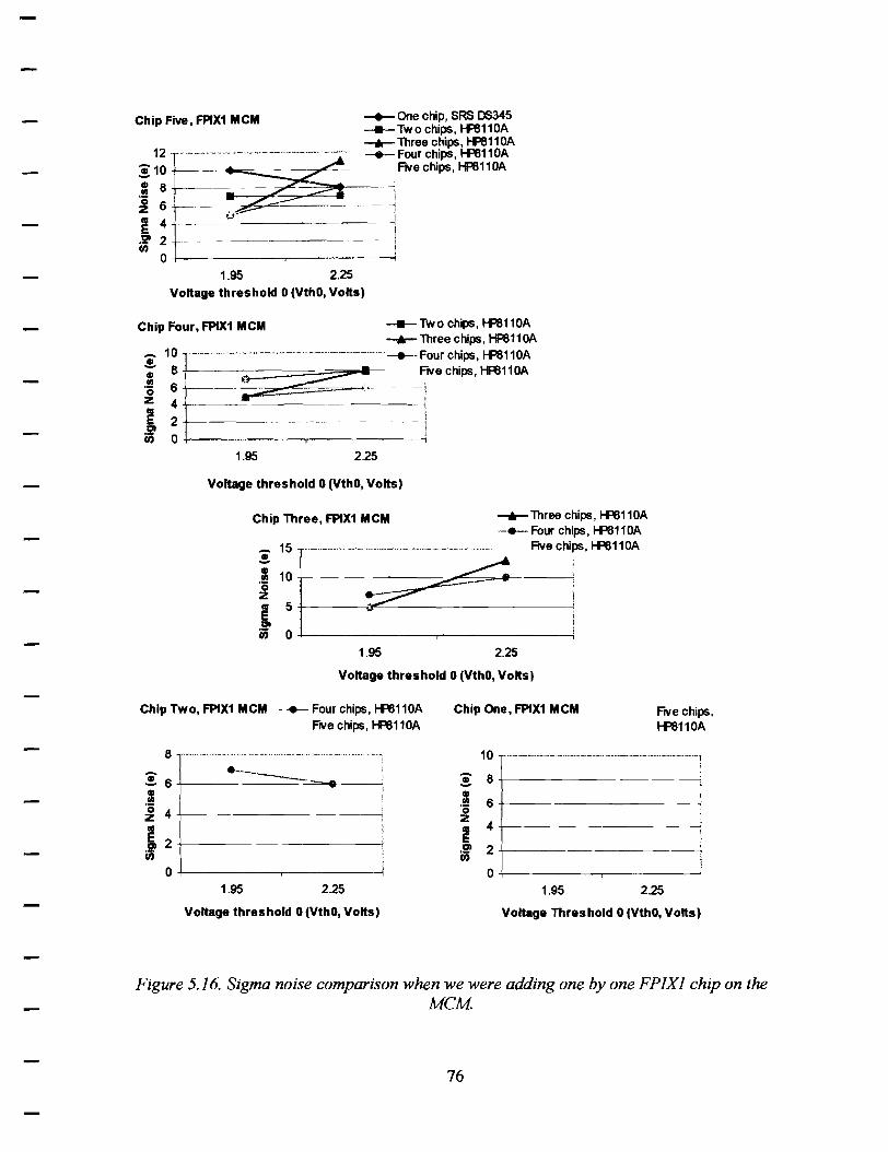
Chip Five, FPIX1 MCM -+-One chip, SRS 00345 ---Two chips, l-F8110A
12 -..-. Three chips, l-F8110A ---- Four chips, l-F811 OA
~10 FIVe chips, tff110A GI 8 .!! 0 6 z " 4 E i .2' 2 en
+---------------!
0 1.95 2.25
Voltage threshold 0 (VthO, Volts)
Chip Four, FPIX1 MCM --- Two chips, l-F811 OA ......- Three chips, tff110A
~ 10 ·-·---·--·-·-·- ····---····-··--··-·--· .. --·- - -+--Four chips, l-F811 OA
GI 8 1-----;.;=::====::;:;;::=i~t-- F1Ve chips, tff110A ·~ 6 :·----4 z 4 E" 2 -+------- i ~ 0 ----------i
1.95 2.25
Voltage threshold O (VthO, Volts)
Chip Three, FPIX1 MCM
1.95
......- Three chips, l-F8110A ---Four chips, l-F8110A
Ave chips, l-F8110A
2.25
Voltage threshold 0 (VthO, Volts)
Chip Two, FPIX1 MCM ---- Four chips, l-F8110A FIVe chips, l-F8110A
Chip One, FPIX1 M CM Five chips, l-F8110A
10 -·--·------·--·-·---·-···· .. ··--·-··-.. ------·-·-·-1
-. ------.!. 6 +-------- ....c-=-•---' .I ~ 4
e .!21 2 +-----(/)
1.95 2.25
Voltage threshold O(VthO, Volts)
I
~ 8 --- --------i 6 .,....._ __ ---------<
4
1.95 2.25
Voltage Threshold O (VthO, Volts)
Figure 5.16. Sigma noise comparison when we were adding one by one FPIXJ chip on the MCM
76
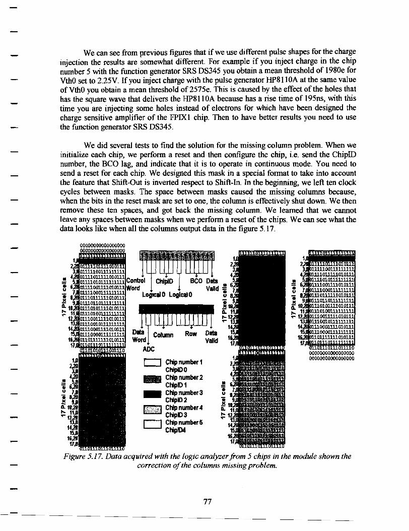
We can see from previous figures that if we use different pulse shapes for the charge injection the results are somewhat different For example if you inject charge in the chip number 5 with the function generator SRS DS345 you obtain a mean threshold of 1980e for VthO set to 2.25V. If you inject charge with the pulse generator HP8110A at the same value ofVthO you obtain a mean threshold of 2575e. This is caused by the effect of the holes that has the square wave that delivers the HP8110A because has a rise time of 195ns, with this time you are injecting some holes instead of electrons for which have been designed the charge sensitive amplifier of the FPIXl chip. Then to have better results you need to use the function generator SRS DS345.
We did several tests to find the solution for the missing column problem. When we initialize each chip, we perform a reset and then configure the chip, i.e. send the ChipID number, the BCO lag, and indicate that it is to operate in continuous mode. You need to send a reset for each chip. We designed this mask in a special format to take into account the feature that Shift-Out is inverted respect to Shift-In. In the beginning, we left ten clock cycles between masks. The space between masks caused the missing columns because, when the bits in the reset mask are set to one, the column is effectively shut down. We then remove these ten spaces, and got back the missing column. We learned that we cannot leave any spaces between masks when we perform a reset of the chips. We can see what the data looks like when all the columns output data in the figure 5.17.
v.-....,,~"'~LV.._._._.O
Dita Column Row Data Woro Valid
ADC
CJ Ctip number 1 CtiplOO
- Chip number2 CtiplD 1
- Ctip nwnber3 Chlpl02
~ Chip number4 ~ Chlpl03 CJ Ctip numbers
Ctipl04
00000000000000000 00000000000000000
Figure 5.17. Data acquired with the logic analyzer from 5 chips in the module shown the correction of the columns missing problem.
77
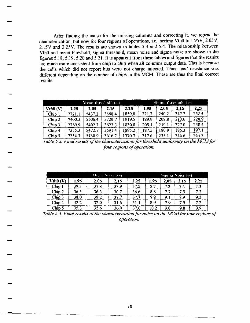
After finding the cause for the missing columns and correcting it, we repeat the characteriz.ation, but now for four regions of operations, i.e., setting VthO to 1.95V, 2.05V, 2.15V and 2.25V. The results· are shown in tables 5.3 and 5.4. The relationship between VthO and mean threshold, sigma threshold, mean noise and sigma noise are shown in the figures 5.18, 5.19, 5.20 and 5.21. It is apparent from these tables and figures that the results are much more consistent from chip to chip when a11 columns output data. This is because the cells which did not report hits were not charge injected. Thus, load resistance was different depending on the number of chips in the MCM. These are thus the final correct results.
5437.2 252.4 7400.3 5506.4 1919.5 224.9 7289.9 5402.2 3623.3 1830.8 209.I 227.0 238.4 7355.3 5472.7 3691.4 1895.2 187.5 180.9 186.3 197.1 7354.3 5430.9 3616.7 1770.7 217.6 235.1 246.6 264.3
Table 5.3. Final results of the characterization for threshold uniformity on the MCMfor four regions of operation.
37.9 37.5 8.7 7.8 7.3 36.5 36.3 36.7 36.6 8.8 7.7 7.9 7.2 38.0 38.2 37.7 37.7 9.8 9.1 8.9 9.2 32.2 32.0 31.6 31.1 8.9 7.9 7.9 7.2 35.3 35.6 36.0 37.6 10.2 9.0 9.8 9.9
Table 5. 4. Final results of the characterizal ion for noise on the MCM for four regions of operation.
78
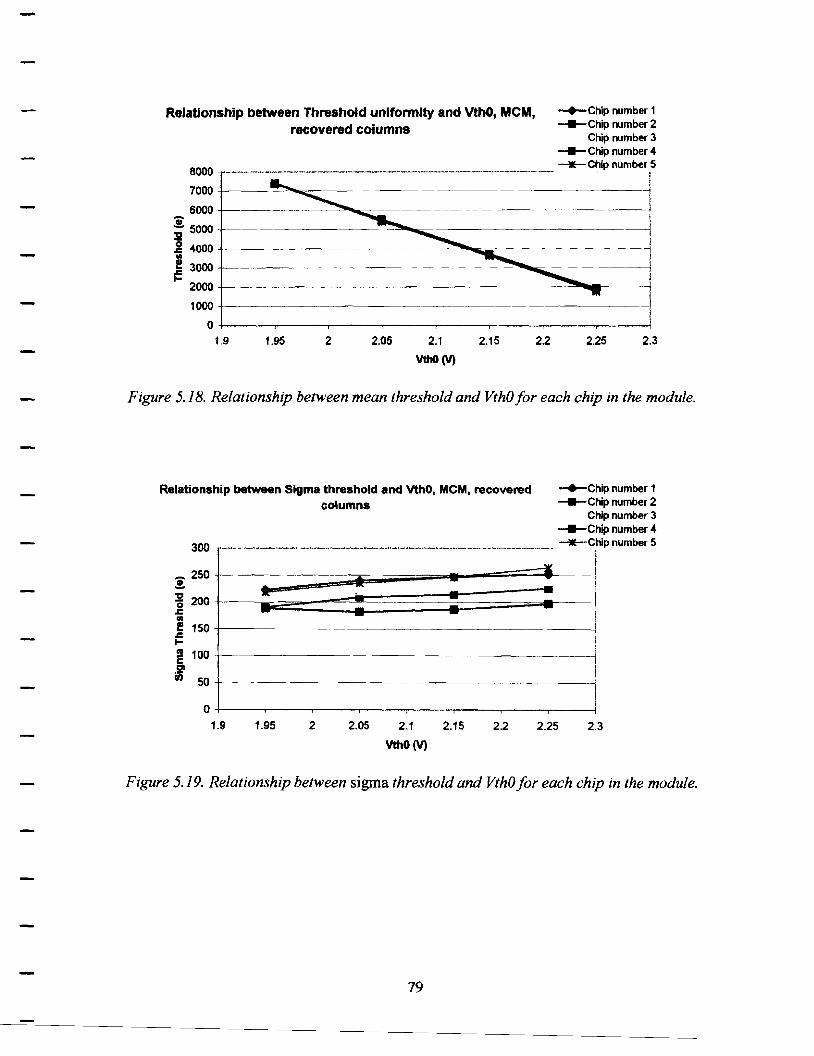
Relationship between Threshold uniformity and VthO, MCM, recovered columns
-+-Chip number 1 -Chip number 2
Chip number 3 -Chip number 4 ~Chip number 5
8000 -------·---·----·--·-------·---------·-·-----·---- l
rooo ~ 6000 +-----
~ 5000 +---- -=-~-------------~ ~ 4000+--------------~ ..... ...------------il "" ~ 3000+-------------------=""'"""-=---------i "'" 1. 2000+----------------------.~--"" ..... --------1
I 1000 +-----------------------------!
O+----.----...-~-...----,---~------~--....;
1.9 1.95 2 2.05 2.1 2.15
VthO (V)
2.2 2.25 2.3
Figure 5. 18. Relationship between mean threshold and VthO for each chip in the module.
Relationship between Sigma threshold and VthO, MCM, recovered columns
-+-Chip number 1 -Chip number 2
Chip number 3 -Chip number 4
300 ,-···---------.. ---------·----·-·-----·-·----·-----·-----·· ~C.hip number 5
~ I ~ 250 1-~~:::;;;;;;;;;+•------~-~-:=:~~:-:--11 ~ 200f---~~:;~;;~::=::::::::::=:=:=-~~;;;;;::::;::--~: en - - } f 150 -+------.c I-
E 100+--------------~ I
~ I ~ 50+----------------------------1
1.9 1.95 2 2.05 2.1
VthO(V)
2.15 2.2 2.25 2.3
Figure 5. 19. Relationship between sigma threshold and VthO for each chip in the module.
79
-+-Chip number 1 Relationship between Noise and VthO, MCM, recovered columns -Chip number 2
Chip number 3
45 -·-·-··--·--------------···---·--··--···------·--.. ··· -Chip number 4 ~Chip number 5
40t------:~;;;;;;;.;::::::~~~----~;~-
l __ J•t'::=::;;~~~,~ ........ ""='====:ti''~~==~~ 35 * • x::::::: _______ --j
··========~·~=======·~==::=~ ........ L___J 30 +-----=------------
~ 25 +------------------------------l
I 0 20+------------------------------------z
15
10+----------------------------------;
5+---------------------------
0+---...,..----,-----,-----.-----.-----.-----.-----l
1.9 1.95 2 2.05 2.1 2.15
VthO (V)
2.2
Figure 5.20. Relationship between noise and VthO for each chip in the module.
Relationship between Sigma Noise and VthO, MCM, recovered columns -+-Chip number 1
-Chip number 2 Chip number 3
12 ·--··--·---.. -····-··--·---------·-···--· ....... -···-----·--··----·--- -Chip number 4 ~Chip number 5
I
-~-~~-~~~~~===x~-1 ------- • : i -----------4~~__:==:::::=-... I
10
:!: 8
6 1111 E CJ) 4 Ci)
2
0 1.9 1.95 2 2.05 2.1 2.15 2.2 2.25 2.3
VthO (V)
Figure 5.21. Relationship between sigma noise and VthO for each chip in the module.
80
5.4 MULTI CHIP MODULE (MCM) WITH SENSOR, THRESHOLD UNIFORMITY AND NOISE TEST
We did the characterization of the MCM mounted on a sensor. The sensor was the Tilel P-STOP designed by the ATLAS experiment at CERN. We repeated the whole procedure with the only difference being that the FPIXl 's were bump-bonded to the sensors. We want to see the effect of the sensors by looking for differences from the results that we got without sensors on the readout chips. Bench tests had shown that chip number 4 on this MCM was in short circuit. Thus in this specific MCM we only had four chips to be characterized. In table 5.5 we summarize all the results obtained for the characterization with sensor, setting the VthO terminal of the chips at 1.95V. We also show as figures 5.22 and 5 .23 the histograms and corresponding gaussian curves of the threshold and noise distribution on the chip number 1 bump-bonded to the sensor. As could be expected, the noise, and thus also the threshold dispersion increases when the pixel cells were bumpbonded to sensors. The mean threshold is also somewhat higher. The very large difference in the mean threshold for chip number 1 and the large threshold dispersion for chip number 3 are not understood. Unfortunately, there was no time to carry out more tests.
340.24
er Noise (e- 14.7 13.91 13.59 10.51 Table 5.5. Threshold and Noise test results over 170 pixel cells, with sensors on it.
;;·t Mean vthM:0.21384 ~\"; Mean vth(e):7823.57 ~,t··. Sigma vthM:0.00930 !'.;~·Sigma vth(e): 340.24
Figure 5.22. Voltage Threshold distribution in the chip number 5 on the MCM with sensors.
81
Mean NolseM:0.00177 Mean Noise(e}: 64.83 Sigma NolseM:0.00029 Sigma Noise(e):10.61
Figure 5.23. Noise distribution in the chip number 5 of the MCM with sensors.
5.5 REPRODUCIBILITY TEST
To know how reproducible the threshold uniformity and noise test is we repeated the characteriz.ation ten times to see the variation between the ten different results, In the following graphs we shows as figure 5.24 the variation of the mean threshold, as figure 5.25 the variation of the sigma threshold dispersion, as figure 5.26 the variation of the noise distribution, and as figure 5.27 the variation of the sigma noise dispersion. Reviewing all these results we can see that there is not a significant variation between the ten results of each of the quantities characterized. We can therefore say that the characterization is reproducible. All these results were obtained with the MCM without sensors on it.
Mean Threshold -Chip number 1 -Chip number 2 -6-Chip number 3
7000 ------------~~--~------~---~-------· --~ -ti-Chip number 4 ~ _._Chip number 5 ll 6900 - ! Q 4
..c:: 6800 \ J 6100 L_..._~~~~~~~~~~~~_J i ssoo+----..-t1t--.._...,_... ....... ._ ..... ....,,,,.~...,.,.,._~-------i e 6soo _,_---,.----.---.,--..-....,---,.---____,
0 2 6 8 10 12
Test number
Figure 5.24. Mean threshold variation
82
---Chip number 1 -Chip number 2 Sigma Threshold
:! 300
_._Chip number 3 -M-Chip number 4 -+-Chip number 5
"a
~ 250 Ill
! s:. .. 200 1!11 E Cll ii 150
0 2 4 6 8 10 12 Test number
Figure 5.25 Sigma threshold variation
-Chip number 1 -Chip number 2
Mean Noise
50 -r-----------_._Chip number 3 -It-Chip number 4
9 -+-Chip number 5 - 45-+-~~~~~~~~~-~~~~~~~~------11
J g 40r-~;_:jr::::a:::::t::::tr:::!::::t===ir:=:t::t~-----j i 35+.-_s;~~ .... ~~~~~'::::'-~~~~~--I ~~~~t::::!~~:::~~~~~
0 2 4 6 8 10 12
Test number
Figure 5.26. Mean noise variation
Sigma Noise _,._Chip number 1 -Chip number 2 _._Chip number 3
1 o --·-·---·----- -ti-Chip number 4 -&-Chip number 5
9 +---&-C>-0--0-<>-~-0~~-0---0f--~---!' a +-____.,....,1r-•:--11~ .... -11t---::-:._-11'.__J1-W-----i 7-1-------llF-i....-:~--~a-::----~~---~----1
6 +-4'--~--f;i!F------5 +-~~~~----~~--~~~-----!
4+----..--~.,---....--~....---,.------4
0 2 4 6 8 10 12
Te•t number
Figure 5.27. Sigma noise variation
83
5.6 ffiTS STUDIES
This test has been developed to know the influence on the results of the number of injections that you are input to each pixel cell in order to obtain the characterization. We did the characterization with 50, 100, 250, 500, 750 and 100 hits (injections). In the following graphs we show as figure 5.28 the results of the fluctuations on the results of the mean threshold distribution, as figure 5.29 the fluctuations of sigma threshold, as figure 5.30 the fluctuations for the noise distribution, and as figure 5.31 the fluctuations for the sigma noise. We can then demonstrate that there is no significant fluctuation in the results above 500 hits. Then in the following characterizations we used only 500 hits. This test was perfonned with the MCM without sensors on it.
Mean Threshold tluctualiol'ls respect to hits number _.....Chip number 1 for each chip on the MCM _.....Chip number 2
........-chip number 3
or~--;-T 1~i: 0 100 200 300 400 500 600 700 800 900 1000 1100
Hits number
Figure 5.28. Mean threshold fluctuations respect to hits number for each chip on the MCM
Sigma Threshold fluctuations respect to hits number for each chip on the MCM
-CJrip nuni>er 1 -Chip nuni>er 2 -+-Chip nuni>er 3 ~Chip nuni>er 4 --+-Chip nuni>er 5
~ I 0 100 200 300 400 500 600 700 800 900 1000 1100
tits number
Figure 5.29. Sigma threshold fluctuations respect to hits number for each chip on the MCM
84
Mean Noise fluctuations respect to hits number for each chip on the MCM
:i 45 . I •• g 40
• • • c
35 II
~ )( )(
30
--4-- Chip nurrt>er 1 ----Chip nurrt>er 2 _.__Chip nurrt>er 3 ~Chip nurrber 4 -e-etiip nurrt>er 5
•
0 100 200 300 400 500 600 700 800 900 1000 1100
tfts number
Figure 5.30. Mean noise fluctuation respect to hits number for ach chip on the MCM
Sigma Noise fluctuations respect to hits number for each chip on the MCM
15~--·
:i13 •
--4-- Chip nurri>er 1 --4-- 01ip nurrber 2 _.__Chip nurrber 3 ~Chip nurrber 4 -e-Chip nurrber 5
_J
·~11 T---~-----~--~~~----~---1
Z9~~~~~__, ! 7 +-~--""""=-- l
0 5-t----ir---r--.--~..,..--,.....---,-~--,--....---.----.---; 0 100 200 300 400 500 600 700 800 900 1000 1100
lits number
Figure 5.31. Sigma noise fluctuations respect to hits number for each chip on the MCM
S.7 OTHER STUDIES ON THE MCM
To understand whether we had a hit during the readout we did a scan each 2ns during the full readout clock cycles with the function generator SRS DS345. The threshold and noise test was done over the pixel cell 8,60 of the chip number 5 on the MCM. A sketch of the readout when we were using the function generator SRS DS345 is shown as figure 5.32.
85
Figure 5.32. Readout with the function generator SRS DS345
To do this test we performed an upgrade of the general software we had designed for the characterization. We included an extra subroutine that controls the data generator that allows it to do a scan of only one cycle of clock pulse each 2ns. The data generator DG2020A has a function called delay. With this function you can delay the pulse that serves as a trigger for the function generator. You can cycle though delaying each time by an additional 2ns with start and end times selected by the user. In this case we did the test for full readout cycles. We did this test for only one pixel cell of one chip on the MCM. The pixel cell was column 8, row 60, and the chip was chip number 5. The results are shown as follows in figure 6.33 for the threshold fluctuations and 6.34 for the noise fluctuations for the pixel cell tested in the chip tested.
86
Threshold Pixel Cell (8,60), chip number 5, SRS DS 345
:!:8650---~~~~~~~~~~~~~~~~~~~~~
"C
] 8600+-~~~~~~~~~~~~~~~~~~~~----; Ii ... ¢: 8550 t----tlhl..-....-i~T:.....:::::!:~~~~~--..,-.~r----1
8450--~_,_~--t--r--t-~-t-~-t-~-+-~-+--r---~--~--~
132300 p235d I I
I I
132ttOO ; j 324sq
pulse lpositi;n (ns)I I
I I I I
I 132POO
ReadClk 251\.fllz
l._____ BCOClk 6.25MHz
Figure 5.33. Threshold variation with an extra injection during the readout.for the pixel cell (8,60) of the chip number 5 on the MCM
87
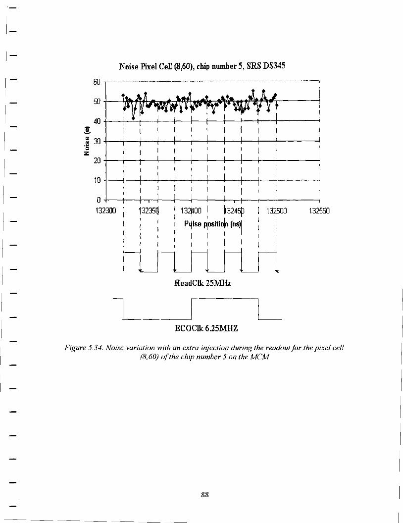
Noise Pixel Cell (8 160), chip number 5, SRS DS345
60 ------------------------------------------------ ------------··1 I
!
1i -~ 30+-~l---+~-+-~-+-~-i---+~-+-~-r-~t----1r--~~-----i ·s z
O-r--~t----r-.---i-~-t-~-r--r-~-+---.--+-~1---.,,---~~____,
132300 . 13235Q n2roo I b245jJ P~lse ~ositio~ (ns)I
I I I ·1
1321500 132550
I
ReadCik 25Wfz
l,_______ BCOCik 6.251\.lliZ
Figure 5.34. Noise variation with an extra injection during the readout for the pixel cell (8,60) o(lhe chip number 5 on the MCM
88
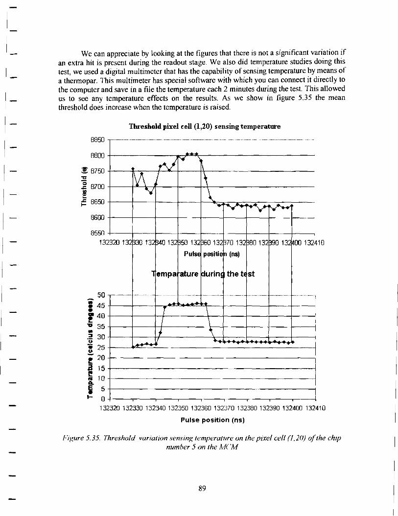
We can appreciate by looking at the figures that there is not a significant variation if an extra hit is present during the readout stage. We also did temperature studies doing this test, we used a digital multimeter that has the capability of sensing temperature by means of a thermopar. This multimeter has special software with which you can connect it directly to the computer and save in a file the temperature each 2 minutes during the test. This allowed us to see any temperature effects on the results. As we show in figure 5.35 the mean threshold does increase when the temperature is raised.
8850
8800
:!: 8750 "C c .c I .... .c I-
8700
8650
8600
8550 13
50 -; 45 • l 40 "CJ 35 • . :! 30 u .. 25 u - 20 ! a 15 s 10 A.
i 5 I- 0
Threshold pixel cell (1,20) sensing temperature
~-··--··----"---·---·--·--·---·-····-·--.----------. -----·---· --·-·--- ·····-·-----·-----·--··-·· ---··--·-· --·--- ----·-· ---- .. ., ______ ····-- ___ .. ___ -----------------------·---
............_ .....
N ._.,.
~
\
~ 7 ' ~ l ...... rv""...- v ._ -,,. ~ ........
2320 132 1330 132 340 132 350 132 360 132 1370 132 380 132 390 132 400 132 410
Puls1:1 positio ,.. (ns)
lempa ature durins thetE st
---- -------- ------~-- ,..-.--------- -------------1 & - ... -
T \ I \ t ' 7 '" - - . - - . -- -~ T ~~~
~ ....
132320 132330 132340 132350 132360 132370 132380 132390 132400 132410
Pulse position (ns)
Figure 5.35. Threshold variation sensing temperature on the pixel cell (l.20) of the chip number 5 on the MCM
89
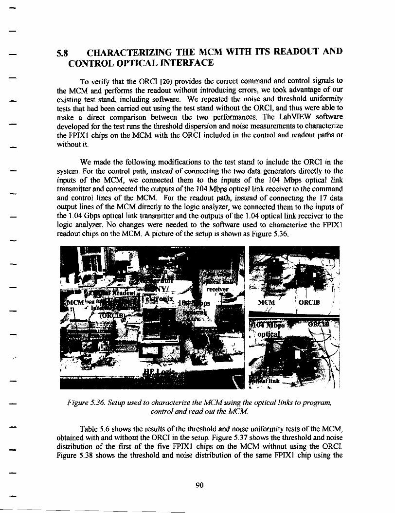
5.8 CHARACTERIZING THE MCM WITH ITS READOUT AND CONTROL OPTICAL INTERFACE
To verify that the ORCI [20) provides the correct command and control signals to the MCM and performs the readout without introducing errors, we took advantage of our existing test stand, including software. We repeated the noise and threshold uniformity tests that had been carried out using the test stand without the ORCI, and thus were able to make a direct comparison between the two performances. The Lab VIEW software developed for the test runs the threshold dispersion and noise measurements to characterize the FPIXl chips on the MCM with the ORCI included in the control and readout paths or without it.
We made the following modifications to the test stand to include the ORCI in the system. For the control path, instead of connecting the two data generators directly to the inputs of the MCM, we connected them to the inputs of the 104 Mbps optical link transmitter and connected the outputs of the 104 Mbps optical link receiver to the command and control lines of the MCM. For the readout path, instead of connecting the 17 data output lines of the MCM directly to the logic analyzer, we connected them to the inputs of the 1.04 Gbps optical link transmitter and the outputs of the 1.04 optical link receiver to the logic analyzer. No changes were needed to the software used to characterize the FPIXl readout chips on the MCM. A picture of the setup is shown as Figure 5.36.
Figure 5.36. Setup used to characterize the MCM using the optical links to program, control and read out the MCM
Table 5.6 shows the results of the threshold and noise uniformity tests of the MCM, obtained with and without the ORCI in the setup. Figure 5.37 shows the threshold and noise distribution of the first of the five FPIXI chips on the MCM without using the ORCI. Figure 5.38 shows the threshold and noise distribution of the same FPIXl chip using the
90
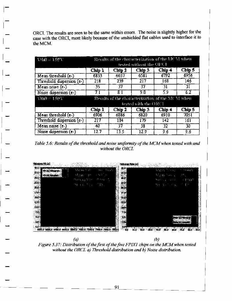
ORCI. The results are seen to be the same within errors. The noise is slightly higher for the case with the ORCI, most likely because of the unshielded flat cables used to interface it to theMCM.
\'thO - l g~y RPsult;;; of the dtdt<trtet imtio11 uf thP J\ TC''\ T islu-•n tPstPd \\ithout tlie <IR( I
-l&RmEEDllli!'Ellllm!Dllmml
Chipl ChipS Mean thresho d (e- 6886 7051 Threshold dispersion e-) 184 161 Mean noise (e-) 37 32 30 Noise spersion (e- 13.5 9.6 9.6
Table 5. 6: Results of the threshold and noise uniformity of the MCM when tested with and without the ORC/.
(a) (b) Figure 5. 37: Distribution of the first of the five FP IXI chips on the MCM when tested
without the ORCI. a) Threshold distribution and b) Noise distribution.
91
(a) (b) Figure 5.38: Distribution of the first of the five FPIXJ chips on the MCMwhen tested with
the ORCI. a) Threshold distribution and b) Noise distribution.
5.9 CONCLUSIONS
Fermilab has designed and assembled a pixel-readout-chip sub-assembly containing five FPIXl chips with flexible cable interconnections with which to address the technical issues involved in system integration for the proJX>sed BTeV pixel detector. The module contains a total of 14400 pixel ceUs that need to be characterized in order to test the entire module. Software has been developed within the Lab VIEW framework to control a set of instruments to perform threshold and noise tests on aU five readout chips. These tests take only a few hours to run. The software designed to characterize the FPIXl chip for the BTeV experiment is very versatile and very easy to use. The development of this work was very challenge because of the necessity to learn a lot of concepts in instrumentation, Lab VIEW programming, GPIB bus protocols, and the procedures to characterize the FPIXI chip, and later the multi chip module.
The results obtained show that the FPIXl chip's performance is very satisfactory. The only serious problem found was that the last 60 rows in each column did not record hits. This is a feature of the layout that will be corrected on the next submission. The software we developed for the tests is really versatile. At the end of this work we had the chance of using it to perform the characterization including for first time the Optical Readout and Control Interface (ORCI) board designed to control and readout the MCM. We demonstrated that with the ORCI included in the control and readout paths there is no significant variation in the final results of the characterization.
92

GENERAL CONCLUSIONS
• The BTeV experiment will be one of the first experiments in using bidimensional arrays of silicon pixel detectors, because they provide high precision space points and they are quite radiation hard. Radiation hardness is necessary because the detector elements will need to be placed very close to the beam approximately 6mm. The measurements of space points, with very little noise, will provide superior pattern recognition, allowing the experiment to reconstruct tracks and vertices in real time. The BTeV pixel detector will contain about thirty million pixels. The pixel sensors will be arranged in bidimensional arrays and each pixel sensor should be read out by a dedicated electronics cell.
• In order to build the BTeV pixel detector, Fermilab has developed VLSI pixel readout chips containing front-end electronics for every pixel sensor. The pixel chip development involves a succession of steps and submissions toward a chip that meets the BTeV requirements. The chips resulting from these steps are called Fermilab Pixel Readout Chips (FPIX chips) and they have been dubbed FPIXO, FPIXI, and so on. The FPIXI represents the first step towards the final pixel readout architecture. The FPIXI chip is a column-based pixel chip with 50µm x 400µm pixel cells arranged in an array of 160 rows by 18 columns for a total of 2880 pixel cells. Current FPIXI prototypes have sensitive areas of up to 59.2 mm2
.
• The principal integrated circuit is one of the important parts of the pixel detector, the FPIXI chip. We studied the chip itself, describing the way to download and acquire information from it. We have designed all the masks to program it. And, also, we have designed all the command patterns to read out all the data contained in the chip.
• Fermilab has designed and we have assembled a pixel-readout-chip sub-assembly containing five FPIXl chips connected in daisy chain with flexible cable interconnections with which to address the technical issues involved in system integration for the proposed BTeV pixel detector. The module contains a total of 14400 pixel cells that need to be characterized in order to test the entire module and represent the first step to have a complete detector. The sub-assembly containing the 5 FPIXl chips connected in daisy chain is called Multi-Chip Module (MCM).
• To characterize the FPIXI chips contained in the MCM we needed to do the bad pixel map test to know if all the pixels cells are working. Another test that we need to do is the threshold and noise uniformity test, which will give us the mean threshold and the threshold dispersion of the MCM, this test needs to be done for different threshold levels. Also with this test, we can obtain the noise and noise dispersion corresponding to the MCM. As we need to know the reproducibility of this test then we need to repeat many times the threshold and noise uniformity test to know how reproducible it is. In the threshold and noise uniformity test we need to simulate the charge injection produced by the particle crossing (hit), therefore we need to inject charge to simulate
93
these hits, we need to obtain the relationship between the number of hits and the results of the test to see if they affect the results of test.
• We have developed a test stand including the test setup and software to characterize the FPIX 1 chips contained into the MCM. The test stand characterizes automatically the FPIXl chips connected in daisy chain into the MCM. The chain can contain from one until N FPIXl chips. The idea of using the test setup containing general propose instruments will give us the opportunity of using the same setup with a software upgrade to characterize future versions of the FPIX chips.
• The first test stand used to characterize the FPIXI chips took about 157 hours (6.5 days) of running to characterize only one FPIXI chip, which means 786 hours (32 days) of running to characterize 5 FPIX I chips connected in daisy chain. The final version after an optimization of the test setup and software takes only 6 hours of running to characterize an MCM with 5 FPIXl chips connected in daisy chain. And it could be possible decrease the running time injecting more than 17 cells at a time, because the most recently test using a computer with a 750 MHz processor speed shows that the process time is of only about 2 hours of running to characterize a MCM with 5 FPIXI chips connected in daisy chain.
• During the test we found that the FPIXl chips present a inversion in Shit_out respect Shift _in, this feature was affecting the daisy chain producing a bad functionality of the chips. The problem was solved by software, but the designers need to keep in main for future version of the FPIX chips. Another lost of information were the missing columns, which was produced by spaces in the initialization mask. After removes these spaces the FPIXl chips were programmed correctly.
• The bad pixel map test showed that the last 60 rows of all the FPIX I chips did not record hits. This is a feature of the layout that will be corrected on the next submission. The threshold and noise uniformity test showed that the MCM could detect charge injection from 1 OOOe (VthO of about 2.25V) up to 9000e (VthO of about 1. 95V). The mean threshold and the threshold dispersion are consistent from chip to chip. The relationship between the charge injection and VthO was linear for all of the FPIXl chips contained in the MCM. The result of the reproducibility test showed that there is not a significant variation between the results of each of the quantities characterized. We can therefore say that the characterization is reproducible. The hits studies showed that there is no significant fluctuation in the results above 500 hits. Then we suggest that in all the future characterizations will be used only 500 hits. All the above tests were performed with the MCM without sensors on it. As could be expected, the noise, and thus also the threshold dispersion increases when the pixel cells were bump-bonded to sensors. The mean threshold is also somewhat higher. The very large difference in the mean threshold for chip number l and the large threshold dispersion for chip number 3 are not understood. Unfortunately, there was no time to carry out more tests.
• The results obtained shows that the FPIXI chip's performance is very satisfactory. At the end of this work we had the chance of using it to perform the characterization including for first time the Optical Readout and Control Interface (ORCI) board
94
•
designed to control and readout the MCM. We demonstrated that with the ORCI included in the control and readout paths there is no significant variation in the final results of the characterization.
With the design of the test stand to characterize automatically the MCMs of the BTeV pixel detector we are doing a contribution to help that the BTeV experiment comes true.
95
REFERENCES
l. Fermilab's webpage, http://www.fnal.gov/pub/tour.html.
2. Butler J., Stone S., "Proposal for an E,xperiment to Measure Mixing, CP Violation and Rare Decays in Charm and Beauty Decays at the Fermi/ab Collider, Bte V'', Fermi lab Internal document, May 1999.
3. Santoro, A., et al., "BTe V: An Expression of Interest for a Heavy Quark Program at CO", F ermilab Internal document, May 18, 1997.
4. Ed Barsotti, Gustavo Cancelo, Bob Downing and Sergio Zimmermann, "Flex Circuit fhr the Detector Plane Interconnect", Internal Document# ESE-PIX-9981014, October 14, 1998.
5. G. Cancelo, D. Christian, J. Hoff, A. Mekkaoui, R. Yarema, S. Zimmermann, "High readout speed pixel chip development at Fermilab ", Fourth Workshop on Electronics for LHC Experiments, 528-532, 1998.
6. D. Christian "A rad-hard pixel readout chip for the BTeV'', Vertex 2000.
7. J. Hoff, !;PIX/ pad description, Internal Document, November 20th 1998.
8. B. Chou, et al., "(fltra-High-Density Interconnect Flex Substrates", HDI Magazine, December 1998.
9. Glenn F. Knoll, "Radiation Detection and Measurement", John Wiley and Sons, New York, 2nd Edition, c.1989, Chapter 11, pp 337-386.
IO. R.M. Barnett, et all., "Particle physics booklet", American institute of physics, July 1996.
11. Butler J., Stone S., "Proposal for an Experiment to Measure Mixing, CP Violation and Rare Decays in Charm and Beauty Decays at the Fermi/ab Collider, BteV, Appendix A", Fermilab Internal document, May 1999.
12. The ATLAS pixel sensor group, "ATLAS pixel detector, technical design report'', ATLAS experiment at CERN, May 1998.
13. Tektronix, Inc. Reference Manual of the PS2520G.
96
14. SONY/Tektronix, Reference Manual of the GD2020A.
15. Standfor Research Systems, Reference Manual.
16. Hewlett-Packard, Reference Manual.
17. M. Colloms., "General Purpose Interface Bus (GPIB) ", The anchor Press Ltd, 1983.
18. National Instruments Corporation, Lab VIEW Users Manual, 1998.
19. National Instruments Corporation, Lab VIEW Function Reference Manual, 1998.
20. S. Vergara, et all., "Optical Readout and Control Interface for the BTeV Pixel Vertex Detector. "Submitted to NIMA, September 2000.
21. Richardson, J., "The ATLAS pixel on-detector electronics," 5th Workshop on Elect. LHC Exp., Snowmass, pp.83-87, Sept. 1999.
22. Skubi. P., et.al., "Flex circuits for the ATLAS pixel detector," Proc. Pixel98, pp.519-534, Batavia, IL, May 1998.
23. Christian, D.C., et.al., "Development of a pixel readout chip for BTeV," NIM A 435, pp.144-152, 1999.
24. Mekkaoui, A., et.al., "FPIX2: an advanced pixel readout chip," 51h Workshop on Elect.
LHC Exp., Snowmass, pp. 98-102, Sept. 1999.
24. Koopman, N. et.al., "Fluxless No-Clean Assembly of Solder Bumped Flip Chips," 46th ECTC, Orlando, Florida, May 28-31, 1996.
25. Cancelo, G.E., et.al., "Fiber Optic based readout for BTeV's Pixel Detector," to be presented 6th Workshop on Elect. LHC Exp., Krakow, Sept. 2000.
26. ATLAS Inner Detector technical design report, CERN/LHC, pp. 16-17, 1997.
27. G. Tonelli., et. al., "The R&D program for silicon detectors in CMS" Nuclear Instruments and Methods A, Num. 435, pp. 109, 1999.
97
28. Artusso, M. et al., "Some further studies on factors affecting the pixel resolution" BTeV internal note, July 1998.
29. Mekkaoui, M. et al., "Results from the FPIXO chip bump-bonded to the ATLAS pixel detector", Proc. 4th_ Workshop on Electronics for LHC experiment, Rome, Sep. 21-25, 1998.
30. Wrigth, J., et al., "A pixel unit-cell targeting 16ns" LBL-32912, Berkeley, 1992.
31. Mekkaoui, M. et al., "FPIXO: A prototype pixel FE chip at Fermilab" Proc. 3rd_ International meeting front end electronics for high resolution tracking detectors, Taos, NM, Nov. 1997
32. Blanquart, L., et al., "Pixel analog cells prototypes for ATLAS in DMILL technology", Nuclear Instruments and Methods A, 435, pp. 144-152, 1999.
33. Mekkaoui, M. et al., "FPIXl: An advanced Pixel readout chip", FERMILAB Conf-99/280, published in the Proc. of the fifth workshop on electronics for LHC experiments, Colorado, September 20-24, 1999.
34. L.Adams, et al., "2nd RD49 Status report: Study of the radiation tolerance of Ics for LHC", CERN/LHCC 99-8 March 1999.
35. Mekkaoui, M. et al., "Radiation tolerant FE in the TSMC 0.25 µ process" to be published in the proceedings of Pixel 2000, International workshop on Semiconductor pixel detectors for Particles and X-rays, June 5-8, 2000.
36. J. Hoff, et al., "PreFPIX2: Core architecture and results" FERMILAB conference 00/260E, to be published in the proceedings of the IEEE 2000 Nuclear Science Symposium.
37. A. Kulyavtsev, et al., "FPIXO test stand studies of chip characteristics" Internal Doc. BTeV coll., June 14, 1999.
38. S. Vergara, et al., "Optical readout and control interface for the BteV pixel vertex detector", Fermilab preprint FERMILAB-PUB-00-246E, pp. 13, November 2000.
98
Publications
1. M.A. Vargas, M. Sheaff, S. Vergara, "The development of software to characterize the fermilab pixel readout chip for the BTeV experiment", Preceedings of the SOMI XIV CONGRESO DE INSTRUMENTACION, pp. 608-612, Tonanzintla, Puebla, MEXICO 1999.
2. M.A. Vargas, M. Sheaff, S. Vergara, "The development of software to characterize the Fermi lab pixel readout chip, FPIXl, for the BTeV experiment", Accepted to NIMA, November 2000. Fennilab preprint FERMILAB-PUB-00-244E, November 2000.
3. S. Zimmermann, S. Kwan, G. Cancelo, G. Cardoso, S. Cihangir, D. Christian, R. Downing, M. A. Vargas, et al., "Development of high data readout rate pixel module and detector hybridization at Fermi lab", Preceedings of the PIXEL 2000, Genoa, June 2000.
4. G. Cancelo, S. Vergara, M.A. Vargas, et al., "Fiber optic based readout for the BteV's pixel detector'', Preceedings of the LEB Sixth workshop on electronics for the LHC experiment, Cracow, Poland, October 2000.
THE DEVELOPMENT OF SOFTWARE TO CHARACTERIZE THE FERMILAB PIXEL READOUT CHIP FOR THE BTeV EXPERIMENT
M.A. Vargas'. M. Sheaff', S. Vergara' FCFM-BUAP, Apdo. Postal 62-570, Av. San Claudio y 14 sur, Puebla Pue, Mexico
Tel. (5222) 233-2533. Fax (5222) 233-2403. Email: [email protected]
RESUMEN Un detector silicon-pixel ha sido propuesto para ser usado en el primer nivel de disparo del experimento BTeV en Fermilab, USA. El principal objetivo del BTeV es llevar a cabo estudios de precision de violaci6n CP y raros decaimientos de quar1<s b y c. Las dimensiones de cada pixel deben ser muy pequeiias aproximadamente 50 m x 400 m con la finalidad de obtener la resoluci6n requerida por los dispositivos con tecnologia VLSI. Celdas pixel con las mismas dimensiones han sido diseiiadas y construidas en sensores, conteniendo cada sensor 2880 canales, la tarea de caracterizarfos es un reto al potencial consumo de tiempo. El software ha sido desarrollado en LabVIEW y controla un grupo de instrumentos para efectuar las pruebas de umbral y ruido sobre todo el chip en menos de una semana de funcionamiento.
Abstract A silicon pixel detector has been proposed to be used in the first level trigger of the BTeV experiment at Fermi/ab. The BTeV main goals are to measure mixing, GP violation and rare decays in the b and c systems. The size of each pixel must be very small, approximately 50 m x 400 m to achieve the required resolution. VLSI chips with pixel ceUs of the same dimensions have been designed and built to instrument the sensors. Since each chip contains 2880 channels, the task of characterizing them is challenging and potentially time consuming. Software has been developed within the Lab VIEW framework to control a set of instruments to perform threshold and noise tests on a full chip in less than one week of running.
1. INTRODUCTION The BTeV experiment has been proposed for the C-Zero interaction region of the Tevatron at Fermilab. A sketch of the apparatus is shown in Fig. 1 a. The magnet that we will use, called SM3, exists at Fermilab. The other important parts of the experiment indude the vertex detector, the RICH detectors, the EM calorimeters and the muon system [1]. The vertex detector is a multi-plane pixel device that sits inside the beam pipe The pixel detector (Fig. 1b) is composed of 93 pixel planes of 100x100mm each, divided into 31 triple-stations perpendicular to the colliding beam and installed a few millimeters from the beam. VLSI pixel readout chips containing front -end electronics for every pixel sensor will be bump-bunded to the detector. Since this detector will be employed for on-line track finding for the lowest level trigger system, the pixel chip will have to read out all detected hits.
The pixel chip development involves a succession of steps and submissions toward a chip that meets the BTeV requirements. The chips resulting from these steps have been dubbed FPIXO, FPIX1, and so on. The FPIX1 represents the first step towards the final pixel readout architecture. The FPIX1 is a column-based pixel chip with 50 m x 400 m pixel cells arranged in an array of 160 rows by 18 columns for a total of 2880 pixel cells. The chip can be divided into three mutually dependent pieces, the pixel cell, the End of Column (EOC) Logic and the Chip Control Logic. A block diagram of the FPIX1 is shown in Fig.2a [2].
1 Scholarship holder of CONACyT, MEXICO/Work developed in a stay at Fermi/ab, PO Box 500, Batavia, ILL, 60510, USA 2 University of Wisconsin, Madison WI 53706, USA/CINVESTAV, Mexico D.F., MEXICO
608

SOMI XIV Congreso de Instrumentacion
BTeV Layout
• Pixel Detector 31 stations of (yxy)
• Wire ChBmbers
Triple! (
·. · alung beam (3 Pi"<el planej:) .... ·.~-. ··· : , . ·. Triple. t position
I Dlpole Magnet Steel Field Integral: 2.6 T-m
Aperature tan II - ±0 .3 RICH: ftourine gas radiator areogel i:reradiator
r ~·--.. · · - · ·· ~ .. +/-6mm gap ~- j -I• I
I Magnet Coils I EM calorimfter beam 1
·-- - ::..,, One Pixel
I Beem Pipe ft;l Muon llbsorber 811d Torcld Plane
Elevation View 0 12 m Pixel Detector 31 stations of Triplets
II 111-~111 -•~I ,;--'--!~_.,...._,.~: ---,--/onetriplet
a) b) Figure 1. a) Sketch of the BTeV spectometer and b) Layout of the BTe V pixel detector.
The pixel cells hold the front-end (Fig. 2b) electronics and the digital interface to the EOC logic (Fig. 2c). The front end contains a charge-sensitive amplifier and a second amplification stage; the output of the second stage connects to a flash ADC and a discriminator. The discriminator output is asserted when the signal at the input of the discriminator is higher than the threshold (Thr). The pixel cell contains a digital interface with two major components, the command interpreter and the pixel token and bus controller. The command interpreter has four inputs corresponding to the four EOC command sets. These commands are presented by the EOC logic simultaneously to all pixel cell interpreters in a column. When an interpreter is executing the input command and the hit output from the discriminator is asserted, the interpreter associates itself with the particular EOC set and simultaneously it alerts the EOC logic to the presence of a hit via the wire-or'ed HfastOR signal. After that. the information is stored in the cell until EOC set issues an output or reset command. When this command is an output command, the interpreter issues a bus request and asserts the wire-or'ed RfastOR signal. Then the balance of the readout proceeds synchronously with the MClk. The EOC logic provides a column token, the token quickly passes pixel cells with no information until it reaches a cell that is requesting the bus. The data is composed of the ADC count bits [3:1] and the row address radd [7:0]. As the hit pixel is read out it automatically resets itself and withdraws its assertion of the RfastOR. This signal returns to its inactivated stale while the last of the hit pixels is being read out [2].
Pixel Cell
Owge Sensitive Amplifier Discriminator
Amplifiec
aj ~ ~ Figure 2. a) FPIX1 Block Diagram, b) Pixel cell squematic and c) Pixel cell digital interface.
609
SOM! XIV Congreso de lnstrurnentaci6n
The FPIX1 chip has 87 pads for external control and data readout. There are eight internal scan paths formed by shift registers with different depths, which we need to fill with information in order to program the chip. Two scan paths are the mask register path that is used to set the programmable reset delay and the mode path which contains the chip mode (triggered mode or continuous mode), the chip ID and the BCO Time Stamp. The last mode path is the Kill/Inject path, which selects the pixel cell or cells to be characterized.
2. CHARACTERIZA llON To characterize the FPIX1 chip we are using a PC with an AT/TNT-GPIB (General Purpose Interface Bus) interface to control the following instruments: Tektronix PS2520G programmable power supply. Hewlett Packard HP16500B logic analyzer system, Stanford Research Systems DS345 30MHz function generator, SONY/Tektronix DG2020A data generator and SONY/Tektronix P3420. The software developed to control all these instruments utilizes the LabVIEW[3] (laboratory Virtual Instrument Engineering Workbench) framework. LabVIEW is a development environment based on the graphical programming language G. It is integrated fully for communication with hardware such as GPIB, VXI, PXI, RS-232, RS-485, and plug in data acquisition boards.
The test stand that we are using to characterize the FPIX1 chip is shown as Fig. 3. The programmable power supply has three outputs. One of them provides power to the digital part of the FPIX1 chip. The second output provides power to the analog part. The last one provides power to the VthO and represents one of the inputs to the discriminators in the front ends. We are using two data generators with programmable outputs to send the information to program the chip. One of them provides data for the Kill/Inject path. The other sends a sequence of commands to the readout stage to acquire the information that the FPIX1 chip delivers. The logic analyzer system receives the information that the chip delivers and stores this information in its memory. The function generator provides the charge to be injected to the selected cells of the FPIX1 chip. We also have two other instruments that it is not necessary to drive by means of the GPIB card. These are a regulated power supply, LEADER 718-SD, which provides power to the vdd/2 input of the FPIX1 to enable single-ended readout, and a current supply made at CPPM, Marseilles. to provide the feedback and Master Bias currents through the inputs marked lvfb and lvbbp.
Figure 3. Test setup to get the threshold uniformity and noise from the FPIX1 chip.
6!0
SOMI XIV Congreso de Instrumentaci6n
We performed the following tests on the FPIX1 chip: bad pixel map, noise, and threshold uniformity. The bad pixel map test is based on injecting charge into all cells on the chip to see what cells are working. First we program the FPIX1 chip to kill all cells except five. By testing five at a time we are able to save time. Then the chip must be programmed to allow charge to be injected into these five cells. Afterwards we inject these cells with a charge level well above the discriminator threshold so that they are expected to register a hit each time that we inject them. This guarantees a response of 100% for correctly working cells. We scan the entire FPIX1 chip in this way five cells at a time to determine which cells are working correcUy and which are not.
The noise and threshold tests are performed together because they use the same data acquisition software. The results shown in this article are from a sample of 170 cells selected from a coarse grid which covers the first 100 raws on FPIX1. Further tests on the full chip are planned. These noise and threshold uniformity tests are based on programming the FPIX1 chip to kill all the pixel cells except five (again to save time), where the five selected are separated from each other by a sufficient distance to remove all possibility of crosstalk between them. Then, as above, we need to program the chip to allow charge to be injected into these five activated cells.After the chip is programmed, we send an injected charge pulse 1000 times and count the number of times we record a hit in each of the five cells. This procedure needs to be repeated in steps of five cells at a time to get the information for all the 170 cells that we choose. We do this for a range of charges above and below the expected threshold. For each level of charge we need to scan all the 170 cells.The levels of charge must be chosen to bracket the voltage threshold. To do this we make a preliminary scan over the chip to determine the optimal range for the test. In our case we fix the VthO at 1.95V and we perform the test over three intervals. For the test reported here, the first one was from 80mV to 200mV in steps of 10mV, the second one was from 200mV to 300mV in steps of 1mV, and the third one was from 300mV to 400mV in steps of 10mV. This means a total of 123 levels of voltage, where the voltages represent the voltage peak-peak of the pulse delivered by the function generator. We can translate these voltages into electrical charge as a function of load. In
our case we have a capacitive load of 6fF. We can calculate the electrical charge injected ( Q,,,jecil in each case by means of Eq. 1.
Qinject = VppC = VppX6Xl0- 15 (1)
After we acquire the data for the 170 pixel cells, we process the information to get the mean and the standard deviation of both the threshold and the noise. Thus, the software developed to do these tests not only acquires the data but also performs the analysis using the data from the FPIX1 chip.
3. SOFTWARE The software is a very important part of the tests, because it is by means of the software that we can control all the phases in the tesl The software to do the bad pixel map works as follows: Initialize all the instruments used in the test. Program the FPIX1 to kill all the pixels cells except five, by means of the first data generator. After that start the logic analyzer and tell it to wait for a trigger. Then tell the second data generator first to inject the charge and then a set time later to send all the commands to do the read out of the FPIX1. Upon receipt of these commands, the FPIX1 begins to send the data generated in response to the injected charge pulses to the logic analyzer. The program waits until this transfer is completed, then reads all the data from the logic analyzer and starts to translate the binary code it provides into a list containing the column and row number from the cells that they are indicating hits. The program repeats this whole procedure over all the 2880 pixels cells in step of five. At the end it generates a list of all pixels that are working, from which we can tell which cells are working and which cells are not.
The software written to perform the noise and threshold uniformity tests for the selected 170 cells on the FPIX1 is divided into two large parts. The first one has the responsibility to acquire all the data from the FPIX1 and the second one performs the analysis of all the data generated to get the mean noise and threshold (defined as the voltage at which we are 50% efficient} with their
611
---- ---------- - --
SOMl XIV Congreso de lnstrumentaci6n
corresponding standard deviations. The data acquisition software is almost the same as for the bad pixel map test. The differences between them are that in the noise and the threshold test we need to inject a pulse of charge 1000 times and read all the data generated by the FPIX1 by means of the logic analyzer. These data are then processed to count the number of times that each cell registers a hit. The software scans the 170 cells in i>teps of five and it repeats the same procedure for each level of voltage selected. The total number of levels for the tests reported here was 123. The data acquired is stored in 42 files that the user specifies with a group name only at the beginning of the program, because the program itself generates an ascending number file, incrementing by one for each new set of five cells. All these files contains the column and row number of each tested cell with its total hit count for each level of voltage delivered from the function generator. The time that take to acquire the data from the 170 cells is 2 days. Note that it would take longer if we did not do five cells at a time and if we did not use two data generators to avoid having to repeat downloading all of the information for each new test. The data processing software calculates the efficiency as a function of the voltage peak-peak by counting the number of hits (of 1000 possible) received. We then perform a least squares fit using the nonlinear LevenbergMarquardt (Lev-Mar) fitting technique on the data for each cell to obtain the best threshold and noise value. The program then performs a statistical analysis using the values from the 170 cells to get the means and standard deviations of the threshold and noise in units of electrons. At the end the program delivers histograms of the noise and thresholds for the 170 cells along with the corresponding gaussian curve.
4. TESTS RESULT ON THE FPIX1 CHIP The bad pixel map test showed that all the cells above row 100 for all the columns are not working. This problem is understood and can be corrected. The threshold uniformity test showed a mean threshold of 9133e with a standard deviation of 292e. The noise test showed a mean noise of 58e with a standard deviation of 7e. Histograms of the data for the 170 cells along with the corresponding gaussian curves are shown as Fig. 4 .
.... c ::I 0
(.)
Voltage threshold (e)
.... c :J 0
(.)
Noise (e)
Figure 4. Test setup to get the threshold uniformity and noise from the FPIX1 chip.
5. REFERENCES
1. S. Stone .• The BTeV program at Fennilab, BTeV pub.note., Fermilab, July 1998.
2. G. Cancelo., 0. Christian., J. Hoff., A. Mekkaoui., R. Yarema., S. Zimmermann., High readout speed pixel chip development at Fennilab, Fourth Workshop on Electronics for LHC Experiments, 528-532, (1998).
3. National Instruments Corporation, LabVIEW Users Manual, (1998)
612
-
Date: Mon, 13 Nov 2000 16:50:47 -0500 From: Pat Moore <[email protected]> To: [email protected] Subject: Acceptance of your (KN0-00-617)
13 November 2000
M. C. Aurora Vargas-Trevino Fermilab MS368 POB 500 Batavia Il., 605 IO
Re: TITLE: The development of software to characterize the Fermilab pixel readout chip, FPIXl, for the BTeV experiment AUTHOR: M. A Vargas, et al. REG. No.: KN0-00-617 R2
Dear Dr. Vargas:
Thank you for returning your revised manuscript to us and for addressing the reviewer comments. Your manuscript has now been accepted and we are sending this final version to the publisher in Amsterdam for future publication in NUCLEAR INSTRUMENTS & METHODS IN PHYSICS RESEARCH (Section A).
Except for your acknowledgement of this acceptance message, further communication about this paper should be addressed to:
Elsevier Science BY NIMA Issue Management POB 2759 1000 CT Amsterdam THE NETHERLANDS Fax: 3 I 20 485 2704 E-mails: [email protected], [email protected]
Please acknowledge receipt of this acceptance via return E-mail.
Best regards, Glenn F. Knoll Editor, NUCLEAR INSTRUMENTS & METHODS IN PHYSICS RESEARCH (Section A) University of Michigan I 906 Cooley Bldg 2104 2355 Bonisteel Blvd Ann Arbor MI 48109-2104 USA
=
The Development of Software to Characterize the Fermilab . ** Pixel Readout Chip, FPIXI, for the BTeV Experiment.
abc * d abc* M. A.Vargas · ·,, M. Sheaff , S. Vergara '''
a Fermi National Accelerator Laboratory, PO Box 500, Batavia, IL, 60510, USA
b Faculty of mathematical and physical sciences-BUAP, Apdo. Postal 62-570, Av. San Claudio y 14 Sur, 72570, Puebla Pue, Mexico
d Physics Department, University of Wisconsin, Madison, WI, 53706, USA
Abstract
Fermilab has designed and assembled a pixel-readout-chip sub-assembly containing five FPIX 1 chips with flexible cable interconnections with which to address the technical issues involved in system integration for the proposed BTeV pixel detector. The module contains a total of l 4400 pixel cells that need to be characterized in order to test the entire module. Software has been developed within the LabVIEW framework to control a set of instruments to perform threshold and noise tests on all five readout chips. These tests take only a few hours to run. PACS: 07.05.-t; 07.05.Hd; 07.05.Kf
1. Introduction We have developed a test stand for use in characterizing the FPIXI front-end
electronics chips that are one version in the FPIX sequence of VLSI chips being developed at Fennilab [I] for readout of the BTeV [2] pixel detector. This detector will provide high-resolution space points near the interaction region for use in reconstructing tracks and vertices. The infonnation the detector provides will be used in the first level trigger to select events that have a high probability to contain secondary decay vertices. This means that all of the hit information from every beam crossing must be made available to the trigger processors. A beam crossing occurs eveiy 132 ns.
In order to achieve the required resolution, ~ 9 pm , the pixel unit cells must not
only be very small, 50j1111 by 400j1111, but the charge deposited in each must also be
digitized and read out. The FPIX chips contain front-end electronics cells with the same dimensions as the pixels on the sensors. The number of FPIX chips which will be bumpbonded to each sensor will depend on the number of cells on each FPIX chip. The FPIXI version of the readout chips contains 2880 cells. Future iterations are expected to contain an even larger number.
If the readout is to be accomplished in the short time between crossings, the information must be sparsified so that only valid hit data is presented to the trigger processors. Which cells are read out is determined by a discriminator in each cell. If a signal above threshold is detected in the cell, then it is read out. The threshold setting for all cells on a single FPIX chip is the same. On FPIX I it is set by a voltage input, called
•• Work supported by the U.S. Department of Energy under contract No. DE-AC02-76CH03000.
c Scholarship holder ofCONACyl: MEXICO. ·corresponding author. Tel.: (630) 840 226/;fax: (630) 840 8208. E-mail address: [email protected].
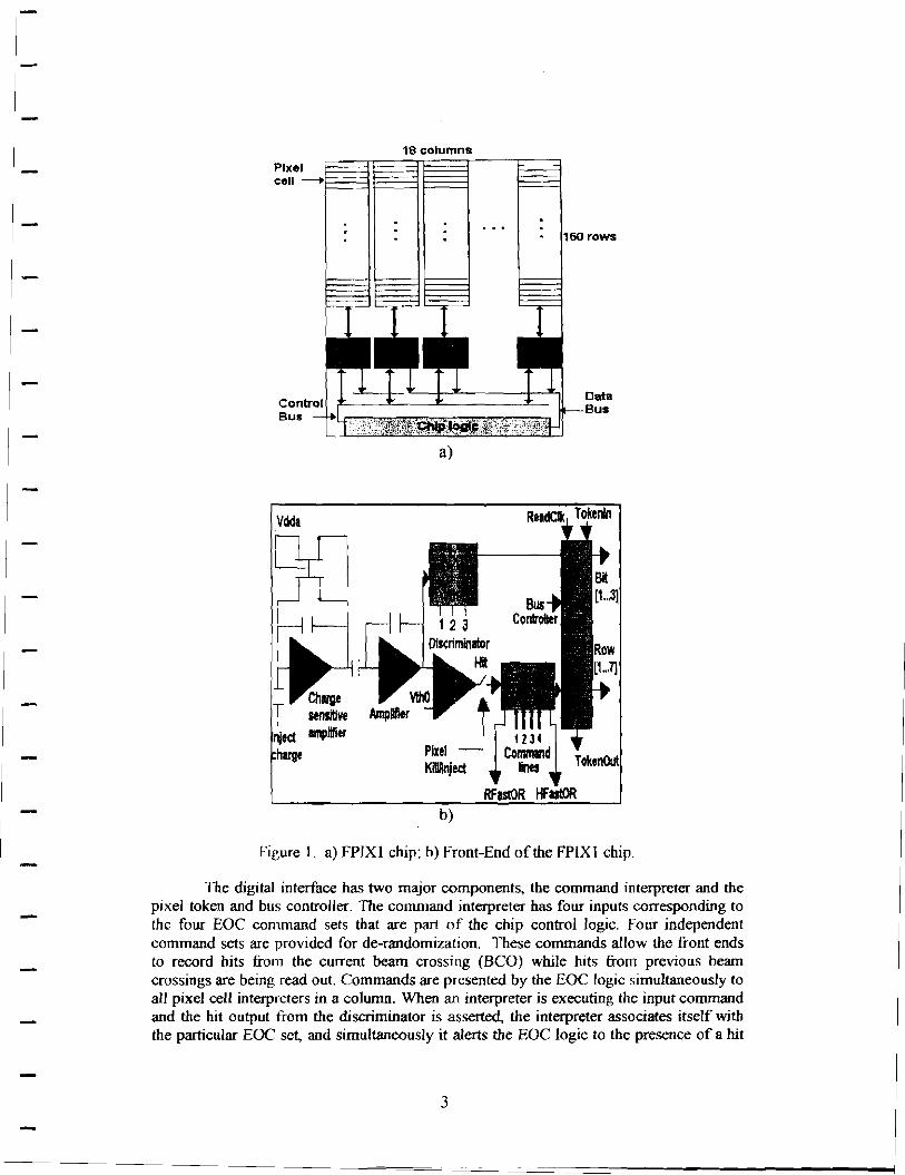
Vdda
nject
18columna
a)
Pixel KiUnjea
b)
160 rows
12 3 4
Data. Bus
eo:'d TokenOut
RFISlOR ~utOR
Figure L a) FPIXI chip; b) Front-End of the FPIXl chip.
The digital interface has two major components, the command interpreter and the pixel token and bus controller. The command interpreter has four inputs corresponding to the four EOC command sets that are part of the chip control logic. four independent command sets are provided for de-randomization. These commands allow the front ends to record hits from the current beam crossing (BCO) while hits from previous beam crossings are being read out. Commands are presented by the EOC logic simultaneously to all pixel cell interpreters in a column. When an interpreter is executing the input command and the hit output from the discriminator is asserted, the interpreter associates itself with the particular EOC set, and simultaneously it alerts the EOC logic to the presence of a hit
3
via the wire-or'ed Hit Fast Or (HfastOR) signal. After that, the information is stored in the cell until the same EOC set issues an output or reset command. When the command is an output command, the inteipreter issues a bus request and asserts the wire-or'ed Read Fast Or (RfastOR) signal.
The readout of hits then proceeds synchronously with the Read Clock (ReadClk). The EOC logic provides a column token; the token quickly passes pixel cells with no hit information until it reaches a cell that is requesting the bus. The cell is then read out. The data is composed of the ADC count bits (3: l] and the row address radd [7:0]. As the hit pixel is read out it automatically resets itself and withdraws its assertion of the RfastOR. This signal returns to its inactivated state while the remaining hit pixels are being read out [I].
The FPIX l chip has 87 pads for external control and data readout. There are eight internal scan paths formed by shift registers with different depths, which we need to fill with information in order to program the chip. Two scan paths are the mask register path, which is used to set the programmable reset, and the mode path which contains the chip mode (triggered or continuous), the chip ID and the BCO Time Stamp. The last two scan paths are the Kill/Inject paths, which select the pixel cell or cells to be characterized. These last two paths go through all pixel cells in the module and are filled by 2880 times 5 shifts of data. 3. Test Procedures a) Overview
The software we have developed takes advantage of the very flexible environment provided by Lab VIEW as well as the advanced data analysis features it provides. While the use of LabVIEW and the relatively slow General Purpose Interface Bus (GPIB) for data acquisition meant that the tests were potentially time-consuming, several time-saving measures were taken that increased testing speed considerably.
First, two personal computers are employed, operating in parallel, both running LabVIEW programs under the Windows NT operating system. The first, PCl, is progranuned for data acquisition. The second, PC2, perf onns the data analysis. The use of a logic analyzer with a Local Area Network (LAN) connection to receive the raw data and pass it on to PC2 makes it possible for the two computers to work simultaneously during the tests.
Second, two data generators are used to send commands to the chips and to the various instruments. This means that only small changes are needed on each cycle and thus a small amount of new information needs to be downloaded per data read cycle. Because of the many cycles involved, this results in a very large reduction in time. The data acquisition program running in PC l synchronizes the action of the two.
We have demonstrated that an adequate characterization of each chip, by which we mean measurements of discriminator threshold uniformity and electronic noise dispersion, can be achieved by charge injecting 10% of the cells in a grid that covers the entire chip uniformly. The threshold and noise results vary randomly within the errors over the chip and do not appear to depend on the location of the cell being tested. We performed an initial test using a very low threshold on all cells to see which cells were working. This test revealed that the last 60 rows in each column did not record hits. This is a feature of the layout that will be corrected on the next submission. Furthennore, the first column on these prototype chips was made to have outputs that could be visualized on an oscilloscope and could not be read out by the EOC logic. Thus there are actually only 1700 cells to be characterized on each FPIX 1 chip ( 17 columns times 100 rows) in the MCM. Ten percent of this is a total of 170 cells to be charge injected on each of the
4
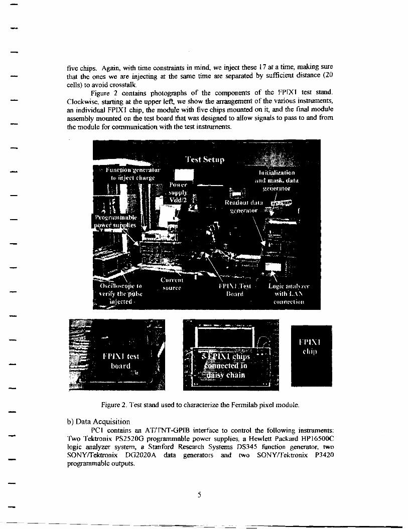
five chips. Again. with time constraints in mind, we inject these 17 at a time, making sure that the ones we are injecting at the same time are separated by sufficient distance (20 cells) to avoid crosstalk.
Figure 2 contains photographs of the components of the FPIXl test stand. Clockwise, starting at the upper left, we show the arrangement of the various instrwnents, an individual FPIXI chip, the module with five chips mounted on it, and the final module assembly mounted on the test board that was designed to allow signals to pass to and from the module for communication with the test instruments.
Figure 2. Test stand used to characterize the Fermilab pixel module.
b) Data Acquisition PC I contains fill ATrrNT-GPIB interface to control the following instruments:
Two Tektronix PS2520G programmable power supplies, a Hewlett Packard HPl6500C logic fillalyzer system, a Stanford Research Systems DS345 function generator, two SONY!fektronix DG2020A data generators and two SONYffektronix P3420 programmable outputs.
5
The test proceeds as follows: The program running in PC 1 first initializes all the instruments used in the test and sets them to their nominal values. The two programmable power supplies provide power to the digital part of the FPIX 1 chips, the analog part of the FPIXl chips, and to all five VthO terminals of the chips on the module. These represent one of the inputs to the discriminators in the front ends. There are also two other instruments that are set manually. These are a regulated power supply, LEADER 718-SD, which provides power to the vdd/2 input of the FPIX l to enable single-ended readout, and a current supply made at CPPM, Marseilles, to provide the feedback and· Master Bias currents.
PC l then initializes the five FPIX l chips using the first of the two data generators. First, it configures the chips in continuous mode, and, since we have several chips connected in daisy chain, it gives each of the chips a unique ID number (ChipID). The FPIX l chips deliver their infonnation in two words, the data word and the control word. The data word contains the ADC value, the colwnn and the row; the control word contains the ChiplD number and the BCO number, which for these tests was always zero. PC 1 then programs the five FPIXls to kill (disable) all the pixels cells except 17 by means of the first data generator. The same data generator is then used to enable charge injection to the 85 cells ( 17 times 5) it has selected. Next PC l sends commands to the logic analyzer to initialize it and to tell it to wait for a trigger that is based on bits in the data format that the chips deliver.
Following this, PCl uses the second data generator to send a trigger to the function generator DS345, which injects charge to each of the enabled cells. Any cell in which this charge produces a signal at the output of the second amplification stage that is greater than VthO will have a hit in the output of its discriminator. The cell then asserts the wire or'ed HfastOR and stores the hit information until the EOC set issues an output command. When this occurs the command interpreter issues a bus request, assens the wire or'ed RfastOR signal, and presents its data on the bus.
The second data generator has also been programmed to send the commands to perform the read out of the FPIXl chips a fixed time after the charge is injected. Upon receipt of these commands, the FPIX ls send the data generated in response to the injected charge pulses to the logic analyzer in the order in which the token passes through them. The logic analyzer acquires the infonnation in binary format and transmits it by means of a LAN connection to the other computer (PC2), which processes the data. For each set of 85 pixel cells PC l repeats the injection of the same charge 500 times and does this for 60 different values of the charge it injects. When all the levels of charge have been scanned, the program changes the selection of the pixel cells and repeats the whole procedure until all 170 pixel cells on each of the five FPIX 1 chips have been scanned.
The levels of charge must be chosen to bracket the voltage threshold. To do this we make a preliminary scan over the chip to detennine the optimal range for the test. For each test we fix VthO at a particular value. We have carried out these threshold wriformity and noise tests in four different regions of operation. c) Data Analysis
PC2 processes the information collected to obtain the mean threshold with its corresponding standard deviation (threshold dispersion) and the mean noise with its C01Tesponding standard deviation for each FPIXl chip on the MCM. When PCl begins to acquire data, PC2 waits until the transfer of information from the first 85 pixel cells finishes, which takes approximately 30 minutes. After this, both programs run at the same time. The data acquisition wait time is 3 S minutes (adding an extra 5 minutes more to avoid any potential conflicts). The data processing program needs to wait for this time
6
only once, because after the first transfer of data both programs can run simultaneously. The information processing takes exactly 30 minutes, so that the times are well matched. Thus, neither PC sits idle for an appreciable time during the test. While PC I is acquiring the data from the current 85 pixel cells, PC2 is processing the information from the previous 85 pixel cells.
Information processing proceeds as follows: First, PC2 translates the binary code that the data acquisition system has acquired into a file that contains the ChipID number, the column number, the row number, the count of hits recorded above threshold and the voltage at each step, as well as the count of total hits (charge injections). Then it calculates efficiency for each pixel cell by dividing the number of counts recorded over the total number of hits. The discriminator output in the front-end of the FPIXl chip is characterized by measuring its response as a function of the charge injected. Although only a single VthO is input to all 2880 cells on a chip, the value of the charge that triggers the discriminator may vary from cell to cell. This represents the threshold dispersion. The electrical charge injected can be calculated using the relationship between voltage and charge produced on the input capacitor. Since we have a capacitive load, C, of 6fF, the
charge, Qinfect , is
Qinfect = VppC = Vpp x 6x10-is coulombs, (1)
where Vpp represents the voltage peak-peak delivered by the SRS DS345 function generator. The number of electrons that correspond to Im V can be obtained by means of the following relationship:
)e = (VppC )e = (Vpp x 6 x IO -is Je (Qilifec/ e- 1.6x10-l9 ' (2)
with the result that
ImV ~ 31.5e. (3)
Because of the inherent noise of the electronics, the efficiency as a function of Vpp has the properties of an error function. For each pixel cell, a fit is perfonned to obtain the error function that best describes the experimental points. Lab VIEW has a library of functions including one that performs a fit using the nonlinear Levenberg-Marquardt (LevMar) method to detennine a nonlinear set of coefficients which minimize chi-square (5]. First, PC2 plots the measured efficiency versus voltage Vpp (charge injected). The initial values of the threshold and noise are obtained using the data. The threshold value, Vthexp , is chosen to be the first value of the voltage that has greater than 50% hit efficiency. For the noise value, PC2 finds the first voltage for which the hit efficiency is greater than 81.5% and subtracts the value for 50% hit efficiency, which yields a exv. These
experimental values are used as the initial guess coefficients for the nonlinear Lev-Mar Fit technique, since the fits will converge more quickly the closer the initial values are to the solutions.
The nonlinear function needs to be specified, i.e., the relationship that describes the error function for each cell as a function of Vpp. For each point, Vpp, along the curve:
7
I vPJ'Pe{w~:t~t]dV err/= 1 v 21fa
2 --<1J
(4)
This technique provides two ways to calculate the Jacobian; i.e., the partial derivatives with respect to the coefficients, needed in the algorithm. These methods are:
Nwnerical calculation: Uses a numerical approximation to compute the Jacobian. Fonnula calculation: Uses a formula to compute the Jacobian. For this one needs to
specify the Jacobian fimctions, which are the partial derivatives of the error function with respect to u and with respect to Vth. These fimctions are:
8errf = (V - Vth )2
- a2 j e 2u2 dV
( )
Vi {(V-Vth)2
]
au &u4 --«:
(5)
(6)
The program repeats the above procedure for all of the pixel cells being tested. When the infonnation for all the pixel cells has been analyzed, the results are output in five files, each of which contains the final information for all cells on one chip in the MCM, i.e., the column number, the row nwnber, the best fit Vth in units of volts and electrons, and the best fit u (noise) in units of volts and electrons. We then run a second program to histogram these quantities for the 170 cells on each of the five chips and to obtain the Gaussian curves that best fit these histograms for each file. We thus obtain the mean threshold, the sigma threshold (threshold dispersion), the mean noise and also the noise dispersion, all in units of volts and electrons for the 170 cells on each FPIX l chip. These results represent the characterization of the chips on the module. A flow diagram of both programs, i.e., the data acquisition program and the data processing program is shown as Fig. 3
8
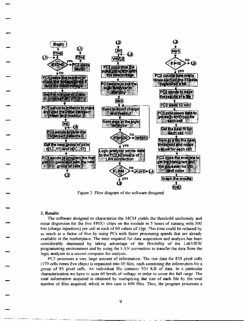
Figure 3. Flow diagram of the software designed.
3. Results The software designed to characterize the MCM yields the threshold uniformity and
noise dispersion for the five FPIX I chips on the module in 5 hours of running with 500 hits (charge injections) per cell at each of 60 values of Vpp. This time could be reduced by as much as a factor of five by using PCs with faster processing speeds that are already available in the marketplace. The time required for data acquisition and analysis has been considerably decreased by taking advantage of the flexibility of the Lab VIEW programming environment and by using the LAN connection to transfer the data from the logic analyzer to a second computer for analysis.
PC2 processes a very large amount of information. The raw data for 850 pixel cells ( 170 cells times five chips) is organized into 10 files, each containing the infonnation for a group of 85 pixel cells. An individual file contains 93 1 KB of data. In a particular characterization we have to scan 60 levels of voltage in order to cover the full range. The total information acquired is obtained by multiplying the size of each file by the total number of files acquired, which in this case is 600 files. Thus, the program processes a
9
total of approximately 550 MB of information to carry out the characterization in each range of operation.
Fig. 4 shows the efficiency versus Vpp for a single pixel cell and the error function that results from the fit to the data. Figures 5 and 6 show the histograms of the threshold and noise dispersion and curves corresponding to the Gaussian fits for one chip mounted in the MCM. Table 1 and Table 2 contain the results of the characterization for the five FPIX 1 chips for four regions of operation.
Efficiency(Eff) vs V~V) Chip number: 1 Column: 1 Row:O Fit\lthM: 0.20962 Flt \lth{e): 7669.<>3473 Fit NoiseM: 0.00093 Fit Noise(e): 30.33957
Figure 4. Error function from one pixel ce11 on one FPlXl chip.
Mean Vth(V): 0.05084 Mean Vth(e): 1859.80799 Sigma VthM: 0.00690 Sigma vth(e): 252.43571
Figure 5. Voltage Threshold distribution in the chip number 1.
IO
Histogram Noise (e)I
20.
7400.3 7289.9 7355.3 7354.3
Mean NoiseM: 0.00103 Mean Noise(e): 37.54008 Sigma NolseM: 0.00020 Sigma Nolse(e): 7.34592
Figure 6. Noise distribution in the chip number l.
5437.2 1859.8 221.7 240.2 247.2 5506.4 3720.7 1919.5 189.9 208.8 213.6 224.9 5402.2 3623.3 1830.8 209.1 219.1 227.0 238.4 5472.7 3691.4 1895.2 187.5 180.9 186.3 197.1 5430.9 3616.7 1770.7 217.6 235.1 246.6 264.3
Table 1. Final results of the characterization for threshold uniformity on the MCM for four regions of operation.
VthO Chi 1 Chi 2 36.6 Chi 3 38.0 38.2 37.7 9.8 9.1 8.9 9.2 Chi 4 32.2 32.0 31.6 31.1 8.9 7.9 7.9 7.2
35.3 35.6 36.0 37.6 10.2 9.0 9.8 9.9 Table 2. Final results of the characterization for noise on the MCM for four
regions of operation.
Acknowledgements The authors wish to thank S. Zimmermann for valuable advice during the course
of this project and G. Chiodini and G. Cardoso for technical assistance. We also want to express our appreciation to the Fermilab staff and management, with special thanks to J. Appel, S. Kwan, and E. Barsotti. This work would not have been possible without the support and encouragement of A. Cordero and A. Fernandez of FCFM/BUAP. The support of the U.S. DOE and CONACyT, Mexico, is also gratefully acknowledged.
11
References [lJ G. Cancelo, D. Christian, J. Hoff, A. Mekkaoui, R. Yarema, S. Zimmennann, High readout speed pixel chip development at Fermi/ab, Fowth Workshop on Electronics for LHC Experiments, 528-532, 1998.
[2] J. Butler, S. Stone, et al., Proposal for an experiment to measure mixing, CP violation, and rare decays in Charm and Beauty particle decays at the Fennilab col/ider- BTeV, submitted to the Fennilab Program Advisory Committee, May 2000. Stage I approval given June 27, 2000.
[3] B. Chou, et al., Ultra-High-Density Interconnect F1ex Substrates, HDI Magazine, December 1998. [4} National Instruments Corporation, Lab VIEW Users Manual, 1998. [5} National Instruments Corporation, lab VIEW Function Reference Manual, 1998
12
Development of High Data Readout Rate Pixel Module and Detector Hybridization at Fermilab
S.Ziinmermann, S.Kwan, G.Cancelo, G.Cardoso, S.Cihangir, D.Christian, R.Downing, J.Hoff, P.Kasper,
A. Mekkaoui, A.Vargas•+, R. Y arema
Fermi National Accelerator Laboratory, Batavia, IL 60510 (USA) *universidad Automona de Puebla, Puebla, PUE 72570 (Mexico)
Abstract At Fennilab, both pixel detector multichip module and sensor hybridization are being developed for the BTeV experiment. The base line design of the module and preliminary results of characterization tests are presented.
1. Introduction
At Fermilab, the BTeV experiment has been proposed for the C-Zero interaction region of the Tevatron [ 1 ]. The innermost detector for this experiment will be a pixel detector composed of 3 1 x2 pixel planes of approximately IOOx IOO mm each, assembled perpendicularly to the colliding beam and installed a few millimeters from the beam. Each plane is formed by sets of three different lengths of pixel hybridized modules, each composed of a single active-area sensor tile and of one row of pixel readout (RDO) integrate circuits (ICs).
The pixel detector will be employed for the lowest level trigger system, hence, the pixel readout ICs will read out all detected hits. This requirement imposes
Work supported by the U.S. Department of Energy under contract No. DE-AC02-76CH03000. •Scholarship holder ofCONACyT, Mexico.
a severe constraint on the RDO IC, hybridize module and data transmission rate to the data acquisition system. Several factors impact in the amount of data that each RDO IC needs to transfer: IC active area, distance from the beam, data format, etc. The final size of the RDO IC is still under consideration.
The BTeV pixel detector is based on a design relying on a hybrid approach. With this approach, the RDO IC and the sensor array are developed separately and the detector is constructed by flip-chip mating of the two together. This offers maximum flexibility in the development process, choice of fabrication technologies, and the choice of sensor material.
2. Proposed Pixel Module
Figure l shows a sketch of the proposed module (top and side views). The module is composed of three layers. The lowest layer is formed by

the RDO I Cs. The back of the I Cs are in thermal contact with the supporting structure while the other side is bwnpbonded to the pixel sensor. The clock, control and power pad interface of the RDO ICs extend beyond the edge of the sensor. The Kapton interconnect circuitry is glued on the top of this assembly and the RDO IC pad interface wired bounded to the circuit. The circuit then extends to one end of the module where the rad-hard module controller and high speed data serializers ICs and fiber optic connectors are assembled [2]. These components are located in this position so that they are outside the tracking volume. ATLAS and CMS explore similar solution [3, 4, 5].
Fiber Optic Cable~
Pixel / Readout IC
Bump Bonds
Controller! / Scrializer
!Cs
Wire Bon~
Figure 1. The Flex Kapton Module
The pixel module readout strategy is paramount to employ the pixel detector in the lowest level trigger. Our present assumptions are based on simulations that describe the track behavior inside the pixel detector. The parameters used for the simulations are: lwninosity of 2x 1032 -2 -I ( d cm s correspon s to an average of two interactions per bunch crossing), pixel size of 400x50 µm, threshold of
2
2000 e- and magnetic field of 1.6 Tesla.
Figure 2 shows a sketch of the 40 I Cs that may compose a pixel half plane. The beam passes on the place represented by the black dot. These numbers assume specific data format and IC size. The distance from the beam to the closest ICs is 6 mm.
Column with
more hits ~'
11 13 17 17 20 18 16 13 8
l Ill 26 31 39 33 25 18 IL 16 20 37 61 76 59 39 26 l!l 17 35 63 141 234 130 65 36 l~
23 35 74 234 -E--Beam
Figu re 2. Average Bit Data Rate, in MB its/sec
The column with more hits requires the biggest data bandwidth. Figure 3 shows the proposed block diagram of the circuit interconnect with the data rate for this column. The serializer IC handles 16 bit words at 60 MWords/sec. There is one dedicated 12 bit data bus connecting the pixel ROO IC with the highest data rate directly to the serializer, another 12 bit data bus that is shared by two ICs and finally a six bit data bus that is shared by the two remaining ICs. The six bit data bus is split between the two serializers. With this interconnect scheme there 1s an additional bandwidth to handle peak data rates and unpredicted hits between 3. l and 4.6 times the required average bandwidth.
Clearly, a high density circuitry is necessary to interconnect the pixel RDO lCs with the controller and serializer ICs. The width of the circuit
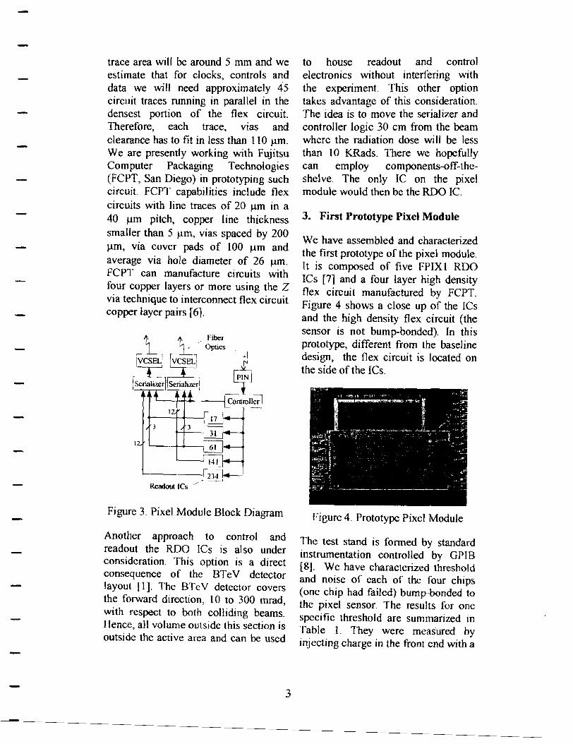
trace area will be around 5 mm and we estimate that for clocks, controls and data we will need approximately 45 circuit traces running in parallel in the densest portion of the flex circuit. Therefore, each trace, vias and clearance has to fit in less than 110 µm. We are presently working with Fujitsu Computer Packaging Technologies (FCPT, San Diego) in prototyping such circuit. FCPT capabilities include flex circuits with line traces of 20 µm in a 40 µm pitch, copper line thickness smaller than 5 µm, vias spaced by 200 µm, via cover pads of l 00 µm and average via hole diameter of 26 µm. FCPT can manufacture circuits with four copper layers or more using the Z via technique to interconnect flex circuit copper layer pairs [ 6].
Readout !Cs
Figure 3. Pixel Module Block Diagram
Another approach to control and readout the RDO ICs is also under consideration. This option is a direct consequence of the BTeV detector layout [ l]. The BTe V detector covers the forward direction, l 0 to 300 mrad, with respect to both colliding beams. Hence, all volume outside this section is outside the active area and can be used
3
to house readout and control electronics without interfering with the experiment. This other option takes advantage of this consideration. The idea is to move the serializer and controller logic 30 cm from the beam where the radiation dose will be less than l 0 KRads. There we hopefully can employ components-off-theshel ve. The only IC on the pixel module would then be the RDO IC.
3. First Prototype Pixel Module
We have assembled and characterized the first prototype of the pixel module. It is composed of five FPIXl RDO ICs [7] and a four layer high density flex circuit manufactured by FCPT. Figure 4 shows a close up of the ICs and the high density flex circuit (the sensor is not bump-bonded). In this prototype, different from the baseline design, the flex circuit is located on the side of the I Cs.
Figure 4. Prototype Pixel Module
The test stand is formed by standard instrumentation controlled by GPIB [8]. We have characterized threshold and noise of each of the four chips (one chip had failed) bump-bonded to the pixel sensor. The results for one specific threshold are summarized in Table I. They were measured by injecting charge in the front end with a
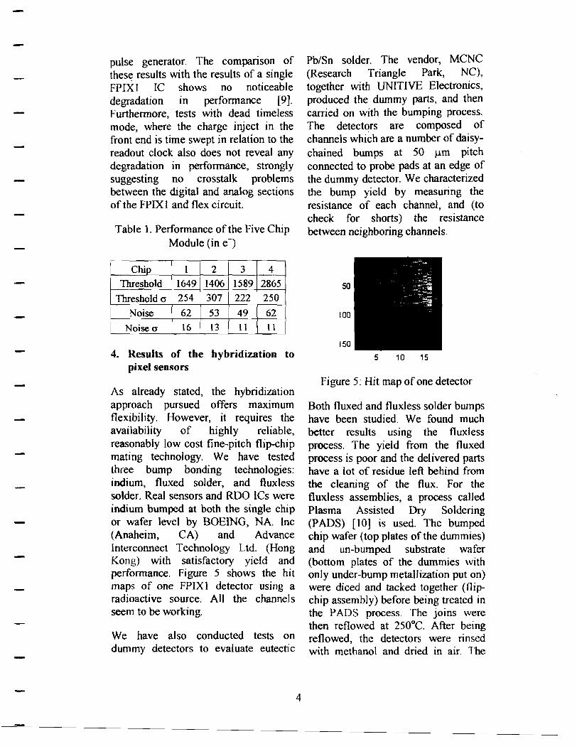
pulse generator. The comparison of these results with the results of a single FPIXI IC shows no noticeable degradation in performance [9]. Furthermore, tests with dead timeless mode, where the charge inject in the front end is time swept in relation to the readout clock also does not reveal any degradation in performance, strongly suggesting no crosstalk problems between the digital and analog sections of the FPIX I and flex circuit.
Table 1. Performance of the Five Chip Module (in e-)
Chip 1 2 3 4 Threshold 1649 1406 1589 2865
Threshold cr 254 307 222 250 Noise 62 53 49 62
Noise a 16 13 l l l l
4. Results of the hybridization to pixel sensors
As already stated, the hybridization approach pursued offers maximum flexibility. However, it requires the availability of highly reliable, reasonably low cost fine-pitch flip-chip mating technology. We have tested three bump bonding technologies: indium, fluxed solder, and fluxless solder. Real sensors and RDO ICs were indium bumped at both the single chip or wafer level by BOEING, NA. Inc (Anaheim, CA) and Advance Interconnect Technology Ltd. (Hong Kong) with satisfactory yield and performance. Figure 5 shows the hit maps of one FPIXI detector using a radioactive source. All the channels seem to be working.
We have also conducted tests on dummy detectors to evaluate eutectic
4
Pb/Sn solder. The vendor, MCNC (Research Triangle Park, NC), together with UNITIVE Electronics, produced the dummy parts, and then carried on with the bumping process. The detectors are composed of channels which are a number of daisychained bumps at 50 µm pitch connected to probe pads at an edge of the dummy detector. We characterized the bump yield by measuring the resistance of each channel, and (to check for shorts) the resistance between neighboring channels.
50
100
150
5 10 15
Figure 5: Hit map of one detector
Both fluxed and fluxless solder bumps have been studied. We found much better results using the fluxless process. The yield from the fluxed process is poor and the delivered parts have a lot of residue left behind from the cleaning of the flux. For the flux.less assemblies, a process called Plasma Assisted Dry Soldering (PADS) [10] is used. The bumped chip wafer (top plates of the dummies) and un-bumped substrate wafer (bottom plates of the dummies with only under-bump metallization put on) were diced and tacked together (flipchip assembly) before being treated in the PADS process. The joins were then reflowed at 250°C. After being reflowed, the detectors were rinsed with methanol and dried in air. The
diameter of the bumps is -40 microns, and the height is -15 microns after mating. We estimate that the single solder bump resistance is less than l Ohm.
Two of the 82 detectors tested were misaligned to cause one bump shift resulting in open channels and shorted adjacent channels. Five detectors had over 50% of their channels open or at high resistance. One was sent to MCNC to be examined. It was taken apart and found to have the bumps on the top plate (chip) not touching the pads on the bottom plate (substrate). This was probably due to contamination or debris on the substrate on that particular location. All this results in an assembly yield of 91.5% (75 good out of 82). For the good detectors, a channel yield of 99.32% or 6.8xl0-3 failedchannel/channel (I 06 open or highresistance channels altogether), and with 14 or 16 bumps per channel and with the assumption that only one bump is bad, a bump yield of 99.95% or 4.5xl0-4 failure/bump.
S. Conclusions
We have described the baseline design and a variation of the pixel module to handle the data rate required for the BTeV experiment at Ferrnilab. The present prototype has shown good electrical performance characteristics.
Indium bump bonding is proven to be capable of successful fabrication at 50 micron pitch on real detectors. For solder bumps at 50 micron pitch, much better results have been obtained with the fluxless PADS processed detectors. The results are adequate for our needs and our tests have validated it as a
5
viable technology.
References
[l] Kulyavtsev, A., et.al., BTeV proposal, Ferrnilab, May 2000.
[2] Cancelo, G.E., et.al., "Fiber Optic based readout for BTeV's Pixel Detector," to be presented 6th Workshop on Elect. LHC Exp., Krakow, Sept. 2000.
[3] Richardson, J., "The ATLAS pixel on-detector electronics," 5th Workshop on Elect. LHC Exp., Snowmass, pp.83-87, Sept. 1999.
[4] Skubi. P., et.al., "Flex circuits for the ATLAS pixel detector," Proc. Pixel98, pp.519-.534, Batavia, IL, May 1998.
[5] Baur, R., "Readout architecture of the CMS pixel detector," see these proceedings.
[6] Chou, B., et.al. "Ultra-HighDensity Interconnect Flex Substrates," HDI Magazine, Marietta, G~ Dec. 1998.
[7] Christian, D.C., et.al., "Development of a pixel readout chip for BTeV," NIM A 435, pp.144-152, 1999.
[8] Vargas, A, "Development of software to characterize the Ferrnilab pixel readout chip, FPIXl, for the BTeV Experiment," to be submitted to NIM.
[9] Mekkaoui, A., et.al., "FPIX2: an advanced pixel readout chip," 5th Workshop on Elect. LHC Exp., Snowmass, pp. 98- l 02, Sept. 1999.
[IO] Koopman, N. et.al., "Fluxless No-Clean Assembly of Solder Bumped Flip Chips," 46th ECTC, Orlando, Florida, May 28-31, 1996.
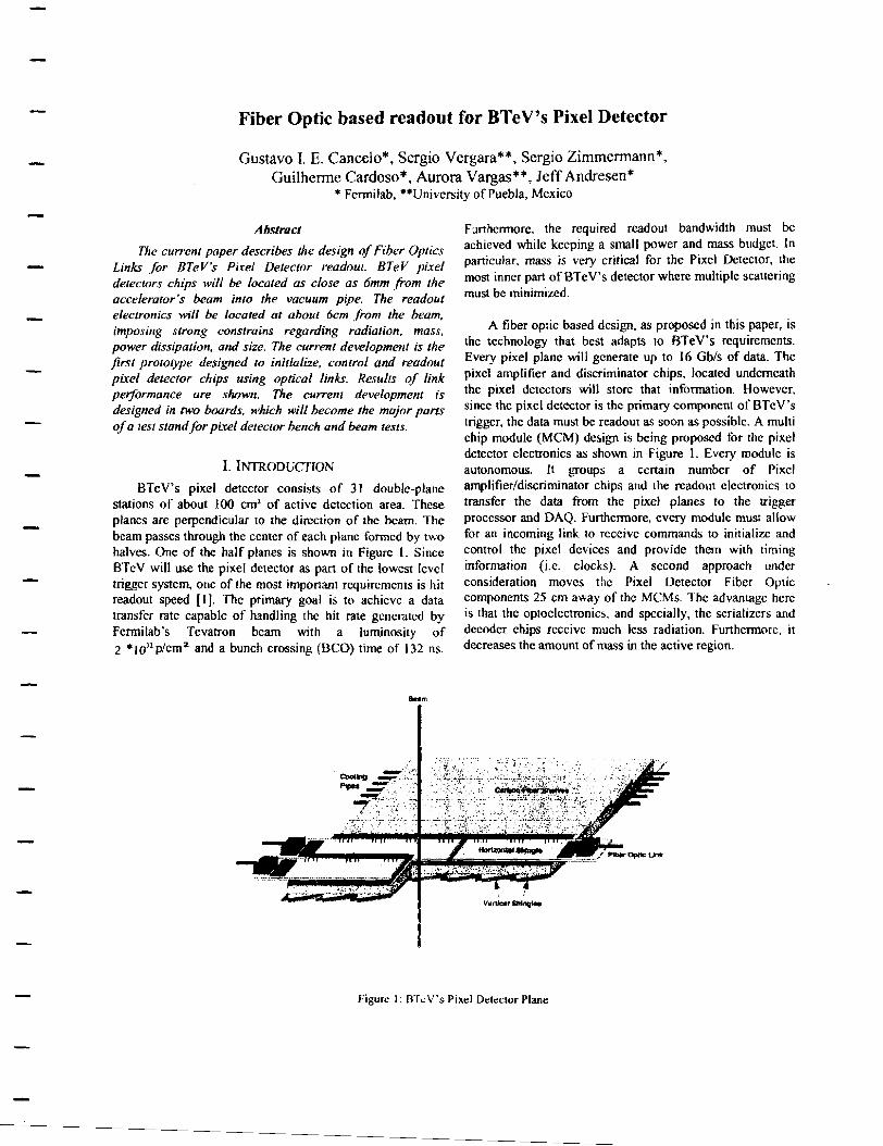
Fiber Optic based readout for BTeV's Pixel Detector
Gustavo I.E. Cancelo*, Sergio Vergara**, Sergio Zimmermann*, Guilherme Cardoso*, Aurora Vargas**, Jeff Andresen*
•Fermi lab, **University of Puebla, Mexico
Abstract
The current paper describes the design of Fiber Optics Links for BTeV's Pixel Detector readout. BTeV pixel detectors chips will be located as close as 6mm .from the accelerator's beam into the vacuum pipe. The readout electronics will be located at about 6cm from the beam, imposi11g strong constrains regarding radiation, mass, power dissipation, and size. The current development is the first prototype designed to initialize, control and readout pixel detector chips using optical links. ResulJs of link performance are shown. The current development is designed in two boards, which will become the major parts of a test stand for pixel detector bench and beam tests.
l. lNTRODUCTlON
BTeV's pixel detector consists of 31 double-plane stations of about 100 cm2 of active detection area. These planes are perpendicular to the direction of the beam. The beam passes through the center of each plane formed by two halves. One of the half planes is shown in Figure I. Since BTcV will use the pixel detector as part of the lowest level trigger system, one of the most important requirements is hit readout speed [I]. The primary goal is to achieve a data transfer rate capable of handling the hit rate generated by fennilab's Tevatron beam with a luminosity of 2 •ion pf cm 2 and a bunch crossing (BCO) time of 132 ns.
&nm
Furthermore. the required readout bandwidth must be achieved while keeping a small power and mass budget. In particular, mass is very critical for the Pixel Detector, the most inner part of BTeV's detector where multiple scattering must be minimized.
A fiber optic based design, as proposed in this paper, is the technology that best adapts to BTeV's requirements. Every pixel plane will generate up to 16 Gb/s of data. The pixel amplifier and discriminator chips, located underneath the pixel detectors will store that information. However. since the pixel detector is the primary component of BTcV's trigger, the data must be readout as soon as possible. A multi chip module (MCM) design is being proposed for the pixel detector electronics as shown in Figure I. Every module is autonomous. It groups a certain number of Pixel amplifier/discriminator chips and the readout electronics to transfer the data from the pixel planes to the trigger processor and DAQ. Furthennore, every module must allow for an incoming link to receive commands to initialize and control the pixel devices and provide them with timing information (i.e. clocks). A second approach under consideration moves the Pixel Detector Fiber Optic components 25 cm away of the MCMs. The advantage here is that the optoelectronics, and specially, the serializers and decoder chips receive much less radiation. Furthennorc, it decreases the amount of mass in the active region.
Figure I: DTcV's Pixel Detector Plane
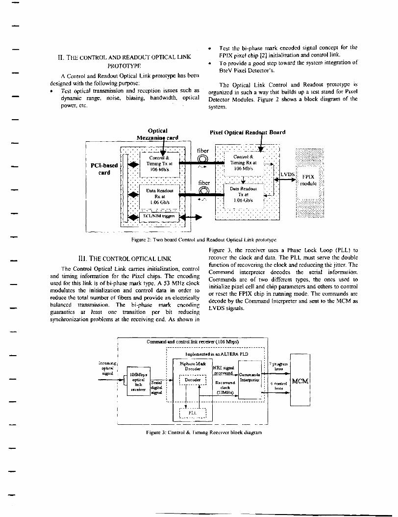
JI. THE CONTROL AND READOUT OPTICAL LINK
PROTOTYPE
A Control and Readout Optical Link prototype has been designed with the following purpose: • Test optical transmission and reception issues such as
dynamic range, noise, biasing, bandwidth, optical power, etc.
PC I-based card
• Test the bi-phase mark encoded signal concept for the FPIX pixel chip [2] initialization and control link.
• To provide a good step toward the system integration of BtcV Pixel Detector's.
The Optical Link Control and Readout prototype is organized in such a way that builds up a test stand for Pixel Detector Modules. Figure 2 shows a block diagram of the system.
Pixel Optical Read t Board
Data Readout T~ at
l.06 Gb/s I .... ..
. _____ !.. . .. "! • •!_. ______ , . . . . . . . . . . .
Figure 2: Two board Control and Readout Optical Link prototype
III. THE CONTROL OPTICAL LINK
The Control Optical Link carries initialization, control and timing information for the Pixel chips. The encoding used for this link is of bi-phase mark type. A 53 MHz clock modulates the initialization and control data in order to reduce the total number of fibers and provide an electrically balanced transmission. The bi-phase mark encoding guaranties at least one transition per bit reducing synchronization problems at the receiving end. As showu in
Figure 3, the receiver uses a Phase Lock Loop (PLL) to recover the clock and data. The PLL must serve the double function of recovering the clock and rcduceing the j ittcr. The Command interpreter decodes the serial information. Commands arc of two different types, the ones used to initialize pixel cell and chip parameters and others to comrol or reset the FPIX chip in running mode. The commands arc decode by the Command Interpreter and sent to the MCM as LVDS signals.
Command end control link receiver (I 06 Mbps) ----- ----- --- - ... ------ -- ---- ---- --- .. ------,
Implemented in anAl..TERA Pl.D ;
Incomtc.1.g optmll signal
BiphaseMllll< Doc oder
figure 3: Contrnl & Timing Receiver block diagram
7 program lmeo

The Control link receiver utilizes a Mite] 1 A354 PIN photodiode operated in photovoltaic mode, connected to· a high speed amplifier and discriminator as shown in Figure 4. The peek optical power in the fiber is lmW. The PIN output signal is about 90m V and the output of the amplifier is 3 70
PIN photodiode Mitel IA354
mV. Figure 5 shows scope images of the optical eye pattern and the bi-phase mark signal decodification at the receiving end. The amplifier used is high bandwidth allowing for a rise and fall time of about 1.5 ns. The PIN's response is very linear up to at least 1.5 mW.
Serial digital signal recovered (CMOS levels)
Figure 4: PIN, amplifier and discriminator
Figure 5: 53 MHz link signals: a) Eye pattern, b) NRZ-b1 phase sent, c) NRZ-bi phase received
A strong constraint on the recovered clock is jitter, because the clock is used to readout pixels and to clock the Gigabit serializcr. Gigabit serializcrs multiply the input clock frequency by 20 but they are unable to reject jitter. A small jitter may represent a big percentage of the output data's period, increasing the bit error rate in the channel. As it can
To - UOG~s n 14011 Acqs 1----~--j-·-~- -----;
!ii LOO V
.
. I . .
I : ~
I
I L.
. --Ji~·., __
A: 64ps
M 200ps Ch'" 1.12V
be appreciated in Figure 6a, the jitter of the recovered clock in the present board is very low, about 64 ps peek-to-peek. The bit error rate of the channel has been measured to be
better than I 0-14 . Figure 6b shows the signal rise and fall
rime of the clock to be around I .OSns.
TO- 10.oc;s1'1; H 11"CI Acq• [ T I
-~~~·~~fi~~l r·-----........ -. -----=---- .......... -I :
i I ' i. ' f
.r\..: I
1.00 v
r • ~ 1. llJn : er l I 0 Olp
I CJf•ll
. \ I " · 1 µI P%~ 1 1 a IJOi.7p
1 CJ Amp.I
A ' 2 '"' V \ / 'v
1
113 171 ·~ CT 24-.lm
:kl S.OOns ChJJ rnv,
Figure 6: a) Cloek'sjitter, b) Clock's rise and fall time
IV. THE READOUT OPTICAL LINK
The readout electronic serializes the data rrom the 5-chip Pixel Module into a G-Link based serial link operating at 1.06 Gb/s. In the final design the G-Link will be replaced by a radiation hardened serializer [3]. Alternative approaches are also being analyzed to relocate the optoelectronics. Extending the L VDS signals from the FPIX module to about 25 cm will allow us to place the optoelcctronics outside the high radiation area. Perfonnance of the G-Link has already been reported in {4].
V. INTEGRATION OF THE OPTICAL LINKS TO THE
READOUT Of A PIXEL MODULE
As shown in Figure 2 the optical links will be used to initialize and deliver commands and clocks to the Pixel chips as well as to readout the pixel data. BTeV Pixel Detector chip characterization has been extensively carried out at Fermilab and is reported elsewhere [5][6]. However, the optical links were integrated with the existing pixel assemblies. Several comparison tests were run using a single FPIX chip and a MCM with 5 pixel devices. Figure 7 shows the current setup.
Figure 7 Ccmtrol and Readout Optical Link prototype setup
Table I compares mean and sigma of noise and threshold of a five-chip FPIX module using two different setups. In the first experiment, the MCM was controlled by a probe station and the data was stored directly into a logic state analyzer. The FPIX initialization panems were generated by a pattern generator, whose outputs were
Mean threshold ( e-) Si ma threshold e-) Mean noise ( e-) s· ( ) ~
directly connected. to the MCM inputs. In the second case, the initialization and control data is provided through the Control Optical Link at 52MHz and the data is readout through the 1.06 Gb/s optical link. Figures 8 and 9 show the comparative histograms of noise and threshold for both tests.
\ thO""" I.'>:'\ Re, ult~ of thl• 1:harat'll'riz:1ti1111 of tht \IC\J "ith Optirnl L111l-.
Chip 1 Chip2 Chip3 Chip4 Chips Mean threshold ( e-) 6906 6886 6820 6910 7051 Sigma threshold (e-) 217 184 179 142 161 Mean noise ( e-) 40 37 38 32 30 Sigma noise (e-) 12.7 13.5 12.9 9.6 9.6
Table J MCM charactenzahon comparison
(b) Figure 8: Five FPIX 1 MCM without using the optical links. a) Threshold distribution and b) Noise Distribution.
(a) (b) Figure 9: Five FPIXI MCM using the optical links. a) Threshold dii;tribution and b) Noise Dii;tribution.
for BTeVNuclear Instruments & Methods in Physics VI. CONCLUSIONS Reascarch A 435 ( 1999) pp 144-152.
A 5 chip FPIX I Pixel Detector Multichip Module has been integrated to be controlled and readout through fiber optics. The first prototypes have proved to have an excellent performance. The readout clock has been recovered from the bi-phase signal with only 65 ps of jitter. This noise is acceptable for clocking a high-speed serializer at 1.06 Gb/s.
The BER of the 106 MB/slink is better than 10-14• EM! and
radiation tests will define the location of BTeV's optoelectronics.
REFERENCES
[I] BTcV: An Expression of interest for a Heavy Quark Program at CO, BTcV collaboration, Ferrnilab, May 18, 1997.
[2] '', G. Cancelo, D. Christian, S. Zimmermann, J. Hoff, A. Mekkaoui, R. Yarerna, "Development ofa pixel readout chip
[3] P. Denes, "Radiation hard gigabit systems", Proceedings of the 2..i Workshop on Optical Readout Technologies for ATLAS, Oxford, Jan. 1999. [4) M.Pearce et al, Development of Radiation Tolerant Gb/s Optical Links for the front-end Read-out of the ATLAS Liquid Argcon Calorimeter, Proceedings of Fourth Workshop on Electronics for LHC Experiments September 1998. [5] G.Cancelo, G.Cardoso, S.Sihanguir, D.Christian, R.Downing, J.Hoff. A.Mekkaoui, A.Vargas, R.Yarema, S.Zimmermann. "Development of high data readout rate pixel module and detector hibriditization at Fcnnilab", Proceedings of PlXEL2000, Genoa, Italy, June 5-8 2000.
[6] M.A.Vargas, M.Sheaff. S.Vcrgara, The Development of Software to Characterize the Fermilab Pixel Readout chip FPIXI for the BTcV experiment. Submitted to Niclear Instruments and Methodcs, Aug. 2000.