liong wai lap - eprints usm
TRANSCRIPT
SILICON NANOPARTICLES SYNTHESIZED VIA
MICROEMULSION WITH VARIOUS
PARAMETERS
LIONG WAI LAP
UNIVERSITI SAINS MALAYSIA
2011
SILICON NANOPARTICLES SYNTHESIZED VIA
MICROEMULSION WITH VARIOUS PARAMETERS
by
LIONG WAI LAP
Thesis submitted in fulfillment of the requirements for
the Degree of Master of Science
January 2011
Name of Candidate: Liong Wai Lap
IC. No.: 840305-06-5385
I declare that the contents presented in this thesis are my own work which was done
at Universiti Sains Malaysia unless stated otherwise. The thesis has not been
previously submitted for any other degree.
Witnessed by:
Signature of Candidate: Signature of Supervisor:
………………………… …………………………
(Liong Wai Lap) (Assoc. Prof. Dr. Sabar Derita Hutagalung)
ii
ACKNOWLEDGMENTS
Here, I would like to take this opportunity to thank those who had helped me
to make this project successfully especially my main supervisor, Assoc. Prof. Dr.
Sabar Derita Hutagalung and my co-supervisor, Dr. Srimala Sreekantan. A lot of
advices and valuable knowledge have been given to allow me to achieve the
proposed goals of this research project. Besides, I would like to express my deepest
gratitude to thank Universiti Sains Malaysia, Engineering Campus, and School of
Materials and Mineral Resources Engineering for the opportunity for allowing me to
complete my master degree of materials engineering. I would also like to thank
School of Biology Science and Mr. Patchamuthu for the use of Transmission
Electron Microscopy and the skillfully characterizations and measurements.
Furthermore, special gratitude is expressed to my dearest friends for their helpful
comments and useful suggestions. I also wish to express my acknowledgement to
Institute of Postgraduate Studies (IPS) which is a graduate centre for Universiti Sains
Malaysia (USM). IPS is also one of the financial assistant for me in completing this
research project which is provided by the USM fellowship In addition, IPS also helps
me in approving the RU grant.
Apart from that, I am very thankful to the technicians and the administration
staffs of the School of Materials and Mineral Resources Engineering who have been
extremely helpful to this research project. Last but not least, I would like to express
my greatest gratitude to Madam Fong Lee Lee, Madam Haslina bt. Zulkifli, Mr.
Abdul Rashid b. Selamat, Mr. Mohammad Azrul b. Zainol Abidin, Mr. Mohd. Azam
b. Rejab, Mr. Mohd. Suhaimi b. Sulong and Madam Hasnah bt. Awang for their
kindness and willingness to help me in achieving the sucess of my research project.
iii
TABLE OF CONTENTS
Page
ACKNOWLEDGMENTS
ii
TABLE OF CONTENTS
iii
LIST OF TABLES
ix
LIST OF FIGURES xi
ABSTRAK
xvi
ABSTRACT
xvii
CHAPTER 1: INTRODUCTION
1
1.0 Overview of nanotechnology and its importance
1
1.1 Challenges in nanotechnology
2
1.2 Silicon nanoparticles
3
1.3 Research objectives
6
1.4 Scope of project
7
CHAPTER 2: LITERATURE REVIEW
8
2.0 Introduction to nanotechnology
8
2.1 Bottom-up and top-down approaches
10
2.2 Nanomaterials
12
2.2.1 Classification of nanostructure materials
13
2.3 Nanoparticle
15
2.3.1 Silicon nanoparticles
16
2.4 Properties of silicon nanoparticles
17
2.4.1 Structural properties
17
2.4.2 Mechanical properties 18

iv
2.4.3 Optical properties
19
2.4.4 Electronic/electrical properties
20
2.4.5 Thermal properties
21
2.4.6 Thermodynamic properties
21
2.5 Synthesis of silicon nanoparticles
22
2.5.1 Mechanical alloying or high-energy ball milling
23
2.5.2 Aerosol synthesis
24
(i) Laser vaporization
25
(ii) Pulsed laser ablation
25
(iii) Plasma reactors
26
2.5.3 Wet chemical synthesis
26
(i) Electrochemical treatment
27
(ii) Chemical etching
27
(iii) Sol-gel synthesis
28
(iv) Microemulsions
29
(v) Solution-based precusor reduction
31
2.6 Synthesis of nanoshell particles/core shell structure
35
2.7 Dispersion of Silicon Nanoparticles
37
2.7.1 Principles of nanoparticles stabilization against aggregation
37
2.7.1 (a)
Interaction forces between particles 38
(i) Van der Waals force
38
(ii) Electrical double-layer interactions
39
(iii) Steric interactions
40
2.7.2 Dispersion methods of nanoparticles
41
2.7.2 (a) Dispersing silicon nanoparticles with a stirred 41
v
media mill
2.7.2 (b) Dispersing and stabilizing silicon nanoparticles
in a low-epsilon medium
41
2.7.2 (c) Production and dispersion stability of
nanoparticles in nanofluids
42
2.8 Factors influence synthesis of nanoparticles
43
2.8.1 Influences of reduction reagents
43
(i) Hydrazine
44
(ii) Sodium borohydride
45
2.8.2 Influences of polymer stabilizer
45
(i) Polyethylene glycol (PEG)
46
(ii) Tetraoctylammonium bromide (TOAB)
47
2.9 Applications of nanoparticles
48
2.9.1 Light-emitting diode (LED)
48
2.9.2 Optical memories
48
2.9.3 Single electron devices
48
2.9.4 Fluorescent Biological Labels
49
2.10 Problems of nanoparticles
49
2.10.1 Determine coverage, thickeness, and uniformity of thin
coating on nanoparticles
49
2.10.2 Determining the surface chemistry of nanoparticles on the
nanoscale
50
2.10.3 Statistical evaluation of dispersion of nanopaticles from
synthesis through manufacturing and into the final
consumer product
50
CHAPTER 3: MATERIALS AND METHODS
52
3.0 Introduction
52
3.1 Materials and equipments 53
vi
3.1.1 Silicon tetrachloride
54
3.1.2 Hydrazine
55
3.1.3 Sodium borohydride
55
3.1.4 Polyethylene glycol (PEG)
56
3.1.5 Tetraoctylammonium bromide (TOAB)
57
3.1.6 Sodium hydroxide
57
3.1.7 Ethanol
58
3.1.8 Acetone
59
3.1.9 Toluene
59
3.1.10 Methanol
60
3.1.11 1-butanol
60
3.1.12 2-propanol
61
3.1.13 De-ionized water
61
3.2 Synthesis of silicon nanoparticles
61
3.2.1 Preparation of reactant solution
61
3.2.2 Hydrazine reduction
62
3.2.3 Precipitation of silicon nanoparticles in colloidal condition
64
3.3 Experimental design
64
3.3.1 Effect of silicon precursor concentration
64
3.3.2 Effect of reducing agents concentration (hydrazine and
sodium borohydride)
65
3.3.3 Effect of surfactant agents [PEG (200 &10000wt%) and
TOAB]
65
3.3.4 Effect of suspension/dispersion solvents
66
3.4 Characterization of silicon nanoparticles
67
3.4.1 Transmission electron microscopy (TEM)
67
3.4.2 Scanning electron microscopy (SEM) 69
vii
3.4.3 Energy-dispersive X-ray spectroscopy (EDX)
70
3.4.4 UV-visible spectroscopy
71
3.4.5 Fourier transform infrared spectroscopy (FTIR)
73
3.4.6 X-ray diffraction analysis (XRD)
74
3.4.7 Raman spectroscopy
76
3.4.8 Electron energy loss spectroscopy (EELS)
78
CHAPTER 4: RESULT AND DISCUSSION
80
4.0 Introduction
80
4.1 Synthesis of silicon nanoparticles
82
4.1.1 Effect of the silicon precursor concentration
82
4.1.2 Effect of reducing agent concentration
90
4.1.2 (a) Effect of hydrazine concentration
90
4.1.2 (b) Effect of the sodium borohydride
98
4.1.2 (c) Comparison between hydrazine and sodium
borohydride
105
4.1.3 Effect of surfactant and capping agent
106
4.1.3 (a) Effect of polyethylene glycol (PEG) amount
[200 wt%]
106
4.1.3 (b) Effect of polyethylene glycol (PEG) amount
[10Kwt%]
117
4.1.3 (c) Effect of tetraoctylammonium bromide
(TOAB) concentration
124
4.1.3 (d) Comparison among the surfactant/ capping
agent (PEG 200wt%, PEG 10Kwt% and
TOAB)
130
4.1.4 Effect of suspension/dispersion solvents
131
viii
CHAPTER 5: CONCLUSIONS AND RECOMMENDATIONS
137
5.1 Conclusions
137
5.2 Recommendations for future work
138
REFERENCES
140
APPENDIX A
153
APPENDIX B
155
APPENDIX C
156
APPENDIX D
157
LIST OF PUBLICATIONS
159
ix
LIST OF TABLES
Table Page
2.1 Classification of nanomaterials with regard to different
dimensions
14
2.2 Some type of classification of nanostructures materials
15
2.3 Test conditions and materials for producing nanofluids
42
2.4 The methods of producing nanofluids 43
3.1 List of chemical used in preparation silicon nanoparticles
53
3.2 List of equipments
54
3.3 The concentration of silicon source in different samples
64
3.4 The different reducing agents sodium borohydride (NaBH4)
concentration
65
3.5 The different reducing agents hydrazine (N2H5OH)
concentration
65
3.6 The samples of different amount of PEG (200wt%)
66
3.7 The samples of different amount of PEG (10000wt%)
66
3.8 The samples of different concentration of TOAB
66
3.9 The samples in different suspension/dispersion solvents 67
4.1
Samples prepared with different concentration of sodium
borohydride
80
4.2 Various samples prepared with different parameters labeling
system
81
4.3 Sample with different silicon precursor concentration
83
4.4 EDX analysis for SiNPs with various concentration of silicon
precursor (Si4+
ions), which was from 0.05M to 0.25M
87
4.5 Detail of UV-visible spectrum for samples with different silicon
precursor concentration
90
4.6 Samples with different concentration of hydrazine (reducing
agent
91
x
4.7 EDX analysis for SiNPs with various concentration of
hydrazine (reducing agent), which were 0.10M, 0.30M, 0.40M
and 0.50M
96
4.8 Detail of UV-visible spectrum for samples with different
hydrazine (reducing agent)
98
4.9 Samples with different sodium borohydride (reducing agent)
concentration
98
4.10 EDX analysis for SiNPs with various concentration of sodium
borohydride (reducing agent), which were sample S10, S11,
S12, and S13
103
4.11
Summary of UV-visible spectrum for samples with various
sodium borohydride (reducing agent) concentration
105
4.12
EDX analysis for SiNPs with various amount of PEG 10000
wt% (surfactant agent & capping agent), which were sample
PE1, PE2, PE3 and PE4
122
4.13
Samples with different concentration of TOAB (surfactant
agent)
124
4.14
EDX analysis for SiNPs with various concentration of TOAB
(surfactant agent), which were sample T1, T2, T3 and T4
128
4.15 Detail of UV-visible spectrum for samples with different TOAB
concentration
129
xi
LIST OF FIGURES
Figure Page
2.1 Top-down and bottom-up approaches
10
2.2 TEM images of SiNPs
17
2.3 Fabrication techniques of silicon nanocrystals
22
2.4 Schematic diagram of the mechanical alloying process
23
2.5 Ball mill for fabrication of nanoparticles
24
2.6 Mechanism of the preparation for core-shell nanoparticles by
C/W/O microemulsion
31
2.7 Variety of core shell particles. (a) Surface-modified core
particles anchored with shell particles; (b) More shell particles
reduced onto core to form a complete shell; (c) Smooth
coating of dielectric core with shell; (d) Encapsulation of very
small particles with dielectric material; (e) Embedding number
of small particles inside a single dielectric particle; (f)
Quantum bubble and (g) Multishell particle
36
2.8 TEM images: (a) PPy -coated Si particles and (b) a magnified
part in the circle along with the inset for the selected area
diffraction (SAD) pattern
37
2.9 Grafting of PEG on SiNPs
47
2.10 Reactiom of TOAB on SiNPs
47
3.1 Structural formula of SiCl4
54
3.2 Structural formula of N2H5OH
55
3.3 Structural formula of NaBH4
56
3.4 Structural formula of PEG
57
3.5 Structural formula of TOAB
57
3.6 Chemical Structure of ethanol
58
3.7 Chemical Structure of acetone
59
3.8
Chemical Structure of toluene 59
3.9 Chemical Structure of methanol 60
xii
3.10
Chemical Structure of 1-butanol 60
3.11
Chemical Structure of 2-propanol 61
3.12
Schematic of water bath setup for the preparation of silicon
nanoparticles
62
3.13 Flow chart for preparation of silicon nanoparticles in PEG
63
3.14
Principle of transmission electron microscopy (TEM) 68
3.15
Principle of scanning electron microscopy (SEM) 70
3.16
Principle of energy-dispersive X-ray spectrometer (EDX) 71
3.17
Principle of UV-visible spectroscopy 73
3.18
Typical apparatus of FTIR spectrometer 74
3.19
Calculation based on Bragg law 75
3.20
Custom built of Raman Spectrometer
78
3.21 Principle of electron energy loss spectroscopy (EELS) 78
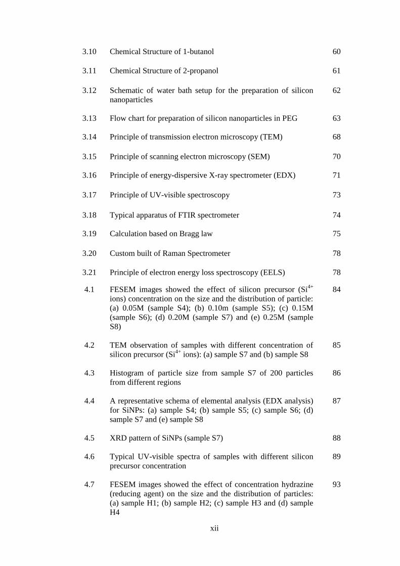
4.1 FESEM images showed the effect of silicon precursor (Si4+
ions) concentration on the size and the distribution of particle:
(a) 0.05M (sample S4); (b) 0.10m (sample S5); (c) 0.15M
(sample S6); (d) 0.20M (sample S7) and (e) 0.25M (sample
S8)
84
4.2 TEM observation of samples with different concentration of
silicon precursor (Si4+
ions): (a) sample S7 and (b) sample S8
85
4.3 Histogram of particle size from sample S7 of 200 particles
from different regions
86
4.4 A representative schema of elemental analysis (EDX analysis)
for SiNPs: (a) sample S4; (b) sample S5; (c) sample S6; (d)
sample S7 and (e) sample S8
87
4.5 XRD pattern of SiNPs (sample S7)
88
4.6 Typical UV-visible spectra of samples with different silicon
precursor concentration
89
4.7 FESEM images showed the effect of concentration hydrazine
(reducing agent) on the size and the distribution of particles:
(a) sample H1; (b) sample H2; (c) sample H3 and (d) sample
H4
93
xiii
4.8 The mechanism of nanodisperse colloid growth of La Mer plot
93
4.9 TEM observation of sample H4
94
4.10 Histogram of particle sizes from sample H4 of 200 particles
from different regions
95
4.11 EDX analysis for SiNPs: (a) sample H1; (b) sample H2; (c)
sample H3 and (d) sample H4
96
4.12 Typical UV-visible spectra of samples with different
hydrazine (reducing agent) concentration
97
4.13 FESEM images showed the sample of SiNPs with various
concentration of sodium borohydride (reduction agent): (a)
sample S10; (b) sample S11; (c) sample S12 and (d) sample
S13
100
4.14 Particle size distribution of SiNPs (sample S10) determined by
SEM analysis
101
4.15 TEM image of the SiNPs (sample S10)
101
4.16 EDX analysis obtained elemental composition of the samples
with various concentration of sodium borohydride: (a) sample
S10, (b) sample S11, (c) sample S12 and (d) sample S13
102
4.17 Raman spectrum of sample S10, which with 0.05M sodium
borohydride
103
4.18 Typical UV-visible spectra of SiNPs with various
concentrations of sodium borohydride: (a) sample S10, (b)
sample S11, (c) sample S12 and (d) sample S13
105
4.19 Model of sample, which grafting with PEG
107
4.20 PEG chain absorbed on SiNPs surface
107
4.21 FESEM images of the SiNPs with PEG addition (a) sample
S22 - 25ml, (b) sample S23 - 50ml (optimum), (c) sample S24
- 75ml and (d) sample S25 – without PEG
109
4.22 Raman spectrum of sample S23 with 50ml PEG addition
110
4.23 Particle size distribution determined by FESEM analysis of
sample S23, which with 50ml PEG addition
111
4.24 FTIR spectrum of SiNPs with 50ml PEG addition (sample
S23)
112
xiv
4.25 EDX analysis on SiNPs with 50ml PEG addition [sample S23]
(elemental composition 32.77 At% silicon, 10.07At% oxide
and 57.16 At % carbon)
113
4.26 Parallel EELS spectra of SiNPs (sample S23) with 50ml PEG
addition: (a) Parallel EELS Si – K (silicon), (b) Parallel EELS
C – K (carbon) and (c) Parallel EELS O– K (oxygen)
114
4.27 TEM images: (a) SiNPs with 50ml PEG addition [sample S23]
(b) a magnified part of SiNPs [sample S23] (PEG-coated Si)
115
4.28 Typical UV-Visible spectra of SiNPs (a) with PEG [sample
S22, sample S23 and sample S24] (b) without PEG [sample
S25]
116
4.29 FESEM images of the SiNPs with PEG addition (a) sample
PE1 – 25g, (b) sample PE2 – 50g, (c) sample PE3 – 75g and
(d) sample PE4 – 100g
118
4.30 Proposed stabilization mechanisme on SiNPs with (a) Stable
uncoated particles (due to electrostatic repulsion), (b) Surface
saturation PEG-coated particle and (c) Agglomeration of
particle due to high amount of PEG
119
4.31 Model representations of SiNPs with different molecular
weight of PEG: (a) high molecular weight of PEG [long
chain], (b) low molecular weight of PEG [short chain]
119
4.32 Particle size distribution determined by FESEM analysis of
sample PE1, which with 25g PEG addition
120
4.33 EDX analysis on SiNPs with PEG 10000 wt% addition, which
is (a) sample PE1, (b) sample PE2, (c) sample PE3 and (d)
sample PE4
121
4.34 Mechanism of the longer chains of higher molecular weight
PEG which have trapped the contamination
122
4.35 UV-Visible spectra for SiNPs with PEG 10000 wt%: (a)
sample PE1, (b) sample PE2, (c) sample PE3 and (d) sample
PE4
123
4.36 FESEM images of the SiNPs with different TOAB
concentration (a) sample T1 – 0.05M, (b) sample T2 – 0.10M,
(c) sample T3 – 0.15M and (d) sample T4 – 0.20M
125
4.37 Particle size distribution of SiNPs (sample T3 - 0.15M TOAB
and sample T4 - 0.20M TOAB), which determined by FESEM
analysis
126
xv
4.38 Mechanism of TOAB in producing smaller size of SiNPs 126
4.39 EDX analysis on SiNPs with TOAB addition, which is (a)
sample T1, (b) sample T2, (c) sample T3 and (d) sample T4
127
4.40 Typical UV-visible spectra of SiNPs with various
concentrations of TOAB
129
4.41 Orientation within the electric field of the light, which
influence the response of the plasmon
129
4.42 FESEM images of the SiNPs, which suspended in different
solvent/dispersion agent (a) sample E1– ethanol, (b) sample
M1 – methanol, (c) sample B1– 1-butanol, (d) sample P1 – 2-
propanol, (e) sample A1 – acetone and (f) sample TO1 –
toluene
132
4.43 Particle size distribution of SiNPs (sample E1, sample M1 and
sample B1), which determined by SEM analysis
133
4.44 TEM image of SiNPs dispersed in ethanol
134
4.45 (a) FESEM image showed the SiNPs which were dispersed in
ethanol, (b) EDX analysis obtained elemental composition of
the particles: 41.91 At% C, 35.31 At% Si and 22.78 At% O
135
4.46 Typical UV-visible spectra of SiNPs with suspended in
various solvents (methanol, 1-buthanol and ethanol)
136

xvi
SILIKON NANOPARTIKEL DISINTESIS MELALUI KAEDAH
MIKROEMULSI DENGAN PELBAGAI PARAMETER
ABSTRAK
Silikon nanopartikel (SiNPs) telah menarik minat penyelidik terutamanya dalam
bidang bioteknologi dan optoelektronik. Objektif kajian ini adalah untuk
menghasilkan SiNPs (<100nm) tanpa gumpalan. Pelbagai parameter telah digunakan
seperti kepekatan ion silikon dan agen penurun, kuantiti agen permukaan dengan
jisim molekul yang berbeza dan pelarut-pelarut organik. Dalam kajian ini, bahan
permula, silikon tetraklorida (SiCl4) dicampurkan dengan penstabil natrium
hidroksida (NaOH), agen permukaan dan agen penurun. Hanya 0.20M SiCl4, 0.50M
hydrazine (N2H5OH), 0.05M natrium borohidrat (NaBH4), 0.15M
tetraoktilammonium bromida (TOAB), 50ml polietilena glicol (PEG) 200wt% dan
25g PEG 10Kwt% dapat menghasilkan penyerakan SiNPs yang baik. Semua SiNPs
telah diuji melalui penyerakan tenaga sinar-X (EDX), mikroskopi elektron imbasan
pancaran medan (FESEM), dan spektroskopi UV-nampak (UV-vis). Manakala,
spektroskopi ’Fourier transform infrared’ (FTIR), analisis pembelauan sinar-X
(XRD), mikroskopi elektron tembusan (TEM), spektroskopi Raman dan spektroskopi
kehilangan tenaga elektron (EELS) hanya untuk sampel yang tertentu sahaja. Bagi
mengurangkan saiz, meningkatkan serakan dan megubahsuai nanovektor bagi aliran
ubat, PEG telah digunakan. PEG 200 wt% telah menunjukkan kesan yang paling
ketara terhadap saiz dan taburan SiNPs dimana struktur kelompang teras telah
dihasilkan. Salutan PEG ini adalah berketebalan 5nm. Etanol merupakan pelarut
yang terbaik dalam penyerakan dimana min saiznya adalah 55.68nm. SiNPs dengan
serakan yang baik telah berjaya dihasilkan dalam kajian ini.
xvii
SILICON NANOPARTICLES SYNTHESIZED VIA
MICROEMULSION WITH VARIOUS PARAMETERS
ABSTRACT
Silicon nanoparticles (SiNPs) have attracted considerable interests from researchers
as it is an interesting material in pharmaceutical and optoelectronic field. Research
objective is to obtain SiNPs (< 100nm) without agglomeration. Various parameters
had been used such as variations of silicon precursor concentrations, reduction agent
concentrations, surfactant agent amounts with different molecular weight, and
different organic solvents. In this study, silicon tetrachloride (SiCl4) was used as a
starting material and mixed with stabilizer sodium hydroxide (NaOH),
surfactant/capping agent and reduction agent. Only suitable concentration and
amount that could be used to produce well disperse SiNPs were 0.20M of SiCl4,
0.50M of hydrazine (N2H5OH), 0.05M of sodium borohydride (NaBH4), 0.15M of
tetraoctylammonium bromide (TOAB), 50ml of polyethylene glycol (PEG) 200wt%
and 25g of PEG 10Kwt%, respectively. All SiNPs had been confirmed by using
FESEM, EDX, and UV-visible spectroscopy. Meanwhile, TEM, FTIR, Raman and
EELS only emphasized on certain SiNPs samples. In order to reduce the size as well
as to improve the dispersion and to modify nanovectors for drug delivery, the PEG
was used. PEG 200wt% had obviously shown the impact and effect on the SiNPs,
which core shell structure had been obtained. The thickness of the PEG coating was
about 5nm. From this study, it also found that ethanol was the best solvent in
disperse of SiNPs which with 55.68nm mean size. Well disperse SiNPs were
successfully synthesized in this study.
1
CHAPTER 1
INTRODUCTION
1.0 Overview of nanotechnology and its importance
Generally, nanotechnology deals with small sized materials or small
structures. The typical dimensions spans from sub nanometer to several hundred
nanometers. The length of a nanometer (nm) is approximately equivalent to one
billionth of a meter, or 1 x 10⁻⁹
m (Itoh 2003).
Nanotechnology is a study of the control of matter in an atomic and
molecular scale. Small features permit more functionality in a given space. Besides,
nanotechnology is not only a simply continuation of miniaturization from micron
scale down to nanometer. Materials in micron size exhibit almost the same physical
properties with the bulk materials. However, due to the high percentage of surface
atoms, nanomaterials exhibit different properties from the bulk materials especially
the properties of electronic, optical, and chemical. Materials in nanosize range
exhibit some specific properties because of a transition from atoms or molecules to
bulk form takes place in the size range. From this transition, it is known that atoms or
molecules have different behaviors from those bulk materials. Besides, the properties
of the former are described by quantum mechanics while the properties of the latter
are governed by classic mechanics. Between these two distinct domains, the
nanometer range is a murky threshold for the transition of a material’s behaviour. For
example, ceramics can easily be deformable when their grain size is reduced to a low
nanometer range which ceramics are normally in a brittle condition. For metal
example, a gold particle of 1 nm across shows red colour. Moreover, a small amount
of nanosize species can bring up the performance of resultant system to an
2
unprecedented level when it interferes with matrix polymer that is usually in the
similar size range. Due to these reasons, nanotechnology has attracted large amounts
of federal funding, research activities and media attention (Cao 2004; Zhao & Ning
2000).
1.1 Challenges in nanotechnology
In 21st century, dynamics and prospects of nanotechnology pose abundance of
challenges not only to scientists and engineers but also to society at large. This is
because nanotechnology has become a rapid emerging and potential growing field.
Besides that, the state-of-the-art philosophical, ethical, and sociological reflection on
nanotechnology which are written by leading scholars from the humanities and social
sciences in North America and Europe. It unravels the philosophical underpinnings
of nanotechnology, metaphysical and epistemological foundations, and conceptual
complexity. In addition, it explores the ethical issues of nanotechnology, its impacts
on human, environmental, and social conditions, and options for reasonable risk
management. It also examines the public discourse on nanotechnology and its related
visions and provides both lessons from the past and outlooks for the future (Cao
2004).
Local growths of nanostructures in both solid state and molecular properties
as well as consideration in controlling of local reactions are the requirement of a
nanomaterial. These have become a great challenge of nanotechnology. Besides that,
dealing with nano interfaces as connections and active components are the second set
of challenges. Furthermore, the concern of novel components of electronic,
mechanical, chemical functionality, energy and information transfer to autonomous
nano systems, theory, in particular computational sciences, for complex nano
3
systems, and others like the nanometer sized liquid-solid interface is also one of the
greatest challenges (Cao 2004).
Thus, it is undeniable that nanotechnology is expanding extensively in our
scientific world. Nano-mechanics and nano-chemistry are expected to forge new
pathways between the 'virtual' world of data processing of all kinds, including
mechanical, chemical and thermal processing, and the 'real' world of sensing and
actuation, bringing about a pervasive wave of new, integrated processing, sensing,
and actuation technologies (Cao 2004).
1.2 Silicon nanoparticles
Currently, the preparation, characterization, and applications of the nanosized
materials have attracted much considerable interests and attention from researchers
in various fields such as physics, biology, chemistry, materials science, and also the
corresponding engineering. Due to the small sizes and large specific surface areas,
nanoparticles usually exhibit in different optical, electronic, and chemical properties
compare with those bulk materials. Nanoparticles have various applications such as
catalysis, electronic, optical, and mechanic devices, high performance engineering
materials, dyes, pigments, adhesives, photographic suspensions, drug delivery and
others (Chen & Wu 2000). These applications bring a lot of advantages to social as
well as industrial uses. Meanwhile, preparation such as controlling of particle’s size,
shape, distribution, crystalinity, and colloidal are taken into consideration at a great
extend by using synthesis methods. It emphasizes that the use of uniform particles
can avoid negative effects from a wide range of particle size distribution.
In this study, silicon nanoparticle (SiNPs) is chosen to be characterized and
investigated because SiNPs are produced by researchers by using various methods
such as gas evaporation, high temperature aerosol reaction, co-sputtering and Si
4
implantation (Leparoux et al. 2007). However, those methods that have been used
involve complex and expensive equipments, high cost materials, long time
consumption and more complicated steps to produce the SiNPs. So, in this study, a
simple, efficient, inexpensive and one pot method (chemical route) has been used to
reduce the material cost, time and equipment complexity which has relatively low
temperature (60oC), reaction time is as short as about 2.5 hours, only few chemicals
are needed such as silicon tetrachloride (SiCl4), sodium hydroxide (NaOH),
polyethylene glycol (PEG), hydrazine (N2H5OH) and ethanol (C2H5OH), and simple
equipments. This concurs with Wu and Chen (2003) in his previous work that,
“Synthesis and characterization of nickel nanoparticles by hydrazine reduction in
ethylene glycol”. Herein, by modification from the original system, we use this
simple, direct and reproducible synthetic method to synthesize SiNPs. Moreover,
SiNPs is chosen because silicon would be a suitable candidate for replacing
fluorescent dyes which labelling in vivo cells and as an alternative to CdSe because
abundant cheap and non-toxic of silicon (Fabbri et al. 2006). Besides, the fluorescent
properties of SiNPs are also of interest for sensing and tagging application especially
for drug delivery (Sudeep, Page & Emrick 2008).
In this project, the size distribution of SiNPs is compared by varying
concentration/amount of precursor, reduction agents and surfactant/capping agents.
Besides, different type of reducing agents and surfactant agents had also been used to
make comparisons. These included N2H5OH, NaBH4, PEG and TOAB.
If nanoparticles surface is not protected with surfactant/capping agent, SiNPs
will possess a considerable surface energy due to the high surface area per unit mass.
Therefore, the most important attribute of this high surface energy is interaction
between particles and results in agglomeration (Yon & Jamie 2008). So, in this study,
5
by using a simple water bath at 60oC, surfactant/capping agent, PEG can be used for
steric stabilization mechanisms, which prevent further aggregation and oxidation of
the particles surface. This is because untreated SiNPs are nearly insulted due to the
oxidation on the surface of particles, which obtain of native passivation shell. The
surface oxidation of SiNPs results in enable interfacial charge transfer and unwanted
perturbation of optical properties (Ogino et al 1999; Gupta & Wiggers 2009). In
addition for stabilization, PEG can be carriers of specific functionalities for further
applications (Poole & Owens 2003; Rotello 2004). Besides, PEG can also cap on the
surface of SiNPs to produce core shell structure nanoparticles, especially for organic
and inorganic hybrid nanoparticles. Thus, it is undeniable that PEG which is a kind
of non-toxic, odourless, neutral and non-irritating agent such as PEG shell on silicon
nanoparticles plays an important role in providing a biocompatible and protective
layer around the particle surface. PEG shell also reduces protein and cell adsorption
(Thangaraja, Savitha & Jegatheesan 2010). This also relates to Feng et al. (2009) that,
“The PEG’s protective layer may prevent aggregation of nanoparticles and
stabilizing nanoparticles”. To prepare the well disperse of PEG coating SiNPs, a
novel PEG system is applied for the preparation of SiNPs (PEG at the lowest
molecular weight, 200 wt% is so far has not been reported as far as to the author’s
knowledge) due to molecular coverage increase with decreasing in PEG molecular
weight (Butterworth, Illum & Davis 2001).
There are various types of organic solvent for suspension/dispersion SiNPs
such as 1-butanol, toluene, 2-propanol and others (Reindl & Peukert 2008; Reindl et
al. 2007; Zhu, Wang & Ong 2001). However, the polarity of the organic solvent
plays a major role in controlling the dispersion level of SiNPs. For example, the
SiNPs tend to agglomerate very easily if suspended in non-polarity organic medium
6
like toluene (Reindl et al. 2008). Suspension in alcoholic solvent is to prevent
oxidation and produce a stable dispersion of SiNPs (Zhu, Wang & Ong 2001). To
clarify the better suspension/dispersion solvents for SiNPs in this study, varying
systems of ethanol, methanol, 1-butanol, 2-propanol, acetone and toluene, separately,
have been studied.
Silicon nanoparticles are characterized by using transmission electron
microscopy (TEM), X-ray diffraction (XRD), UV-Visible spectroscopy, electron
energy loss spectroscopy (EELS), Raman spectroscopy, fourier transform infrared
(FTIR), scanning electron microscopy (SEM) and energy disperse X-ray (EDX).
1.3 Research objectives
The main goal of this study was to synthesis the well dispersed (no
aggregation) SiNPs by using chemical route which was known as bottom up
approach. The synthesis process consisted of (i) generation of supersaturation, (ii)
nucleation and (iii) subsequent growth. PEG was used as capping/surfactant agent
while N2H5OH was a reducing agent in this system. NaOH was used as catalyst and
stabilizer to accelerate the reduction rate to produce more nuclei in low concentration
of precursor.
The main objectives in this study were as following:
- To synthesize silicon nanoparticles (< 100nm ) via a chemical route
- To produce silicon nanoparticles with narrow size distribution (well
dispersed)
- To produce core shell structure (organic and inorganic hybrid
nanoparticles)
7
1.4 Scope of project
Bottom up approach was used to produce SiNPs via chemical route. In this
route, there were four parameters of synthesis of SiNPs which were studied as below:
- Effects of silicon ions concentration
- Effects of reducing agent concentration (N2H5OH and NaBH4,
separately)
- Effects of capping/surfactant agent concentration (PEG 200wt%, PEG
10Kwt% and TOAB, separately)
- Effects of suspension/dispersion solvent (ethanol, methanol, 1-butanol,
2-propanol, acetone and toluene, separately)
These parameters had determined the formation of well disperse, un-
agglomerated particles with controlled size, shape and narrow size distribution of
SiNPs.
For the fabrication and processing of nanomaterials and nanostructures, the
following challenges must be met:
- Overcome the huge surface energy, a result of enormous surface area or large
surface to volume ratio.
- Ensure all nanomaterials with desired size, uniform size distribution,
morphology, crystalinity, chemical composition, and microstructure that
altogether result in desired physical properties.
- Prevent nanomaterials and nanostructures from coarsening through
agglomeration as time evolutes (Cao 2004).
8
CHAPTER 2
LITERATURE REVIEW
2.0 Introduction to nanotechnology
Since the past decades, nanotechnology is an attractive area of scientific
development which covers a wide range of technologies such as research,
development and industrial activity that concerns with structures and processes of a
nanometer scale. A nanometer is one-billionth of a meter (10-9
m) which equals to the
width of three or four atoms, roughly or about one hundred thousand of the width of
a human hair. Besides that, nanotechnology is a multidisciplinary grouping of
physical, chemical, biological, engineering, electronic, processes, materials,
applications and concepts which has a defining characteristic that is one of size
(Dutta et al. 1997). The first concept of 'nanotechnology' was used by a physicist,
Richard Feynman on December 29, 1959 which described that nanotechnology as a
process to manipulate individual atoms and molecules using one set of precise tools
to build and operate another proportionally smaller set down to the needed scale.
Meanwhile, according to Taniguchi (1974), the term of „nanotechnology‟ was
defined as mainly consisted of a process of separation, consolidation, and
deformation of materials by one atom or by one molecule.
However, there is no generally recognized definition of nanotechnology to
date. In a pragmatic approach, the present report uses the following definition:
1. Nanotechnology deals with structures which are smaller than 100 nm (at least
one dimension).
2. Nanotechnology exploits characteristic effects and phenomena which occur
in the transitional zone between the atomic and mesoscopic level.
9
3. Nanotechnology describes deliberate manufacture and manipulation of
individual nanostructures. (El-Shall & Edelstein 1996)
Nanoparticles are the end product of a variety of physical, chemical and
biological processes. Some of the nanoparticles are novel and radically different
from others. Nanoparticle products include:
i. nanotubes
ii. nanowires
iii. quantum dots
iv. „Others‟ nanoparticles
There are four main groups of nanoparticle production processes:
i. Gas-phase
ii. Vapor deposition
iii. Colloidal
iv. Attrition
All of these production processes may potentially expose by inhalation,
dermal or ingestion routes (Aitken, Creely & Tran 2004).
In nanotechnology, there are two main approaches such as „bottom-up‟
approach and „top-down‟ approach. For the „bottom-up‟ approach, materials and
devices are built from molecular components which assemble themselves chemically
using principles of molecular recognition. This approach is primarily featured in
chemistry and biology in dealing with objects of the nanometer scale. Meanwhile,
„top-down‟ approach is a predominant particular in physics and physical technology
which nano-objects are constructed from larger entities without atomic-level control
(Yon & Jamie 2008).
10
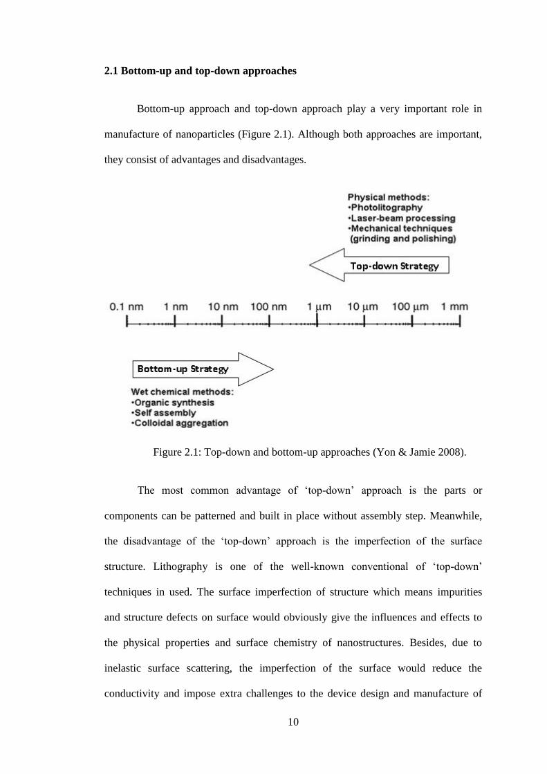
2.1 Bottom-up and top-down approaches
Bottom-up approach and top-down approach play a very important role in
manufacture of nanoparticles (Figure 2.1). Although both approaches are important,
they consist of advantages and disadvantages.
Figure 2.1: Top-down and bottom-up approaches (Yon & Jamie 2008).
The most common advantage of „top-down‟ approach is the parts or
components can be patterned and built in place without assembly step. Meanwhile,
the disadvantage of the „top-down‟ approach is the imperfection of the surface
structure. Lithography is one of the well-known conventional of „top-down‟
techniques in used. The surface imperfection of structure which means impurities
and structure defects on surface would obviously give the influences and effects to
the physical properties and surface chemistry of nanostructures. Besides, due to
inelastic surface scattering, the imperfection of the surface would reduce the
conductivity and impose extra challenges to the device design and manufacture of
11
the nanostructures and nanomaterials. „Top-down‟ approach most likely introduces
internal stress, in addition to surface defects and contaminations. Although there are
many disadvantages, „top-down‟ approach still plays an important role in the
synthesis and fabrication of nanostructures and nanomaterials (Vieu et al. 2000).
Another approach which is used in the synthesis and fabrication of
nanostructure and nanomaterials is „bottom-up‟ approach. There are many „bottom-
up‟ approaches that have been developed to produce nanoparticles which are ranging
from condensation of atomic vapours on surfaces to coalescence of atoms in liquids.
For an example, inverse micelles is one of the „bottom-up‟ approaches (liquid-phase
techniques) which has been developed to size-selected nanoparticles of
semiconductor. Nanostructures and nanomaterials with fewer defects, more
homogeneous chemical composition and better short and long range ordering can
always produce by „bottom-up‟ approach due to driven mainly by the reduction of
Gibbs free energy (Cao 2004).
However, differences in chemical composition, crystallinity, and
microstructure of a material can be clearly portrayed by using different synthesis and
processing approaches. Consequently, the properties of the material also exhibit
differences such as physical properties, optical properties, chemical properties and
mechanical properties.
There are many equipment and tools that have been developed to produce and
characterize the nanostructures and nanomaterials such as scanning electron
microscope (SEM) and transmission electron microscope (TEM). The two early
versions of scanning probes that are launched for nanotechnology are atomic force
microscope (AFM) and scanning tunneling microscope (STM). Scanning confocal
microscope and scanning acoustic microscope (SAM) are other types of scanning
12
probe microscopy that play a crucial role in nanostructures characterization (Cao
2004).
2.2 Nanomaterials
Nanomaterials or nanostructured materials are materials with grain sizes of a
billionth of a meter (1x10⁻⁹
m). Nanomaterials have attracted considerable attention
due to their unique and useful properties. Examples of these properties are lower
melting temperature of semiconductor (Goldstein et al. 1992), increased solid-solid
phase transition pressure in semiconductor nanocrystals (Tolbert & Alivisatos 1995),
lower effective Debye temperature in films of fine particles (Fujita, Oshima &
Kuroishi 1976), decreased ferroelectric phase transition temperature for PbTiO3
(Ishikawa, Yoshikawa & Okada 1988), higher self-diffusion coefficient in
nanocrystalline materials (Horvath, Birringer & Gleiter 1987), changed
thermophysical properties of Ag (Qin et al. 1996) and catalytic activity of metal
oxide nanophase materials (Sarkas et al. 1993).These unique properties of
nanomaterials are determined by their sizes, surface structures and interparticle
interactions. Due to these properties, nanomaterials can be exploited for a variety of
potential applications in fields such as electronic, optoelectronic, chemical, biology,
mechanical and others.
All materials are constituted of grains where, within one grain consists of
many atoms. The average size of an atom is 1 to 2 angstroms (Å) in radius. But for
the ranging grain size of conventional materials are from microns (µm) to several
millimeters (mm). Meanwhile, nanomaterial has grain size from 1 to 100 nanometer
(nm) which 1nm equal to 10 Å. Grain size strongly influences the chemical and
physical properties of the nanomaterial. This is shown when the grain size decreases,
it will increase the volume fraction of grain boundaries or interfaces (Rotello 2004).
13
There are many methods to produce nanoparticles such as:
Sol-gel synthesis
Inert gas condensation
Mechanical alloying or high-energy ball milling
Electrodeposition
Aerosol synthesis
Microemulsion
Co-sputtering
Ion implantation
(Leparoux et al. 2008; Araujo-Andrade et al. 2003; Lam et al. 2000)
2.2.1 Classification of nanostructure materials
The number of dimensions which within nanometer range is the main factor
to classify nanostructure materials and system. There are three systems to confine
particles which are in three dimensions, two dimensions and one dimension. Disc or
platelets, ultra thin films on the surface and multilayered materials which can be
included in system are confined in one dimension. The thin films themselves could
be amorphous, single crystalline or nanocrystalline (Rotello 2004). Besides,
nanowires, nanorods, nanofilaments and nanotubes are the examples of two
dimensions that can be confined in a system. Table 2.1 shows the classification of
nanomaterials with regard to different parameters, which are dimension (3
dimensions, 2 dimensions and 1 dimension), phase composition (single phase solids,
multi phase solids and multi phase systems) and manufacturing process (gas phase
reaction, liquid phase condition and mechanical reaction).
14
Table 2.1: Classification of nanomaterials with regard to different dimensions
(Coffin 2006).
Classification Examples
Dimension
3 dimensions < 100 nm
2 dimensions < 100 nm
1 dimension < 100 nm
Particles, quantum dots, hollow spheres,
etc.
Tubes, fibers, wires, platelets, etc.
Films, coatings, multilayers, etc.
Phase composition
Single phase solids
Multi phase solids
Multi phase systems
Crystaline, amorphous, particles and
layers, etc.
Matrix composites, coated particles, etc.
Colloids, aerogels, ferrofluids, etc.
Manufacturing process
Gas phase reaction
Liquid phase condition
Mechanical reaction
Flame synthesis, condensatin, CVD, etc.
Sol-gel, precipitation, hydrothermal
processing, etc.
Ball milling, plastic deformation, etc.
In principle, a nano-scale dimension can be obtained in all conventional
materials such as metals, semiconductors, glasses, ceramics or polymers. However,
the spectrum of nanomaterials ranges from inorganic, crystalline or amorphous
particles can be found as single particles, aggregates, powders, colloids, suspensions,
emulsions, nanolayers, films and supramolecular structures (dendrimers, micelles or
liposomes). Besides, it also can be found up to the class of fullerenes and their
derivatives. Table 2.2 shows some type of classification of nanostructures materials,
which are cluster, nanocrystals, quantum dots, others nanoparticles, nanowires and
nanotubes.
15
Table 2.2: Some types of classification of nanostructures materials (Brydson &
Hammond 2005).
Nanostructure Size Example Materials
Cluster, nanocrystals,
quantum dots. Radius:
1-10 nm
Insulators,
semiconductors, metals,
magnetic materials.
Others nanopartilces Radius:
1-100 nm
Ceramic oxides,
buckyballs
Nanowires Radius:
1-100 nm
Metals, semiconductors,
oxides, sulfides, nitrides
Nanotubes Radius:
1-100 nm
Carbon, including
fullerences, layered
chalcogenides
2.3 Nanoparticle
In the early 1990s, the term of „nanoparticle‟ was widely used with the related
concepts, „nanoscaled‟ or „nanosized‟ particle. A nanoparticle is a microscopic
particle that defines a particle with diameter smaller than 100 nm in at least one
dimension (El-Shall & Edelstein 1996).
Nanoparticles function as a bridge between bulk materials and atomic or
molecular structures, effectively. Nano-scale materials should not have constant
physical properties if compare with bulk material which is regardless of its size.
Size-dependent properties which are observed are quantum confinement in
semiconductor particles, surface plasmon resonance in metal particles and
superparamagnetism in magnetic particles (are the size-dependent properties which
can be observed). Semi-solid and soft nanoparticles are formed. Liposome is a
prototype nanoparticle of semi-solid nature.
Due to the surface of the material which dominates the properties of the bulk
materials, the properties of materials change when the particle size of materials is
reduced to nanoscale. When the size of material approaches the nanoscale, the atoms
percentage at the surface of a material will become significant. This is because the
16
atoms percentage at the surface of bulk materials (>1µm) is miniscule relative to the
total number of atoms of the material. There are possibilities for the suspensions of
nanoparticles due to their surface interaction with the solvent which come across
with different density. Unexpected visible properties always occur in nanoparticles
due to visible light scattering (Dutta et al. 1997).
Cluster is referred to the nanoparticles at the small end of the size range.
Metal, dielectric and semiconductor nanoparticles have been manufactured, as well
as hybrid structures like core-shell nanoparticles. Nanospheres, nanorods, nanocups,
quantum dots are the types of nanoparticles. For biomedical applications,
nanoparticles are used as drug carriers and imaging agents. There are various types
of liposome nanoparticles which are used as delivery systems for anticancer drugs
and vaccines (Schmid 2004).
2.3.1 Silicon nanoparticles
The fabrication of semiconductor nanoparticles has attracted much
considerable attention due to their potential properties such as physical, chemical,
mechanical, electronic, and optical properties. For example, the optical and
electronic properties of the SiNPs have become a base of the optoelectronic devices
such as applications in light emitting diodes and chemical sensor. SiNPs can be
produced by using gas-phase evaporation, high temperature aerosol reactions, co-
sputtering, Si implantation, ball milling, laser ablation, chemical etching, and gas-
phase pyrolysis (Scriba et al. 2008).
One of the common issues of SiNPs is tendency to agglomerate easily
(especially when dispersed in an organic medium). However, to reduce or prevent
the agglomeration, some techniques such as polymerization and intrinsically stable
suspension have been used which without the application of an additive (Sudeep,
17
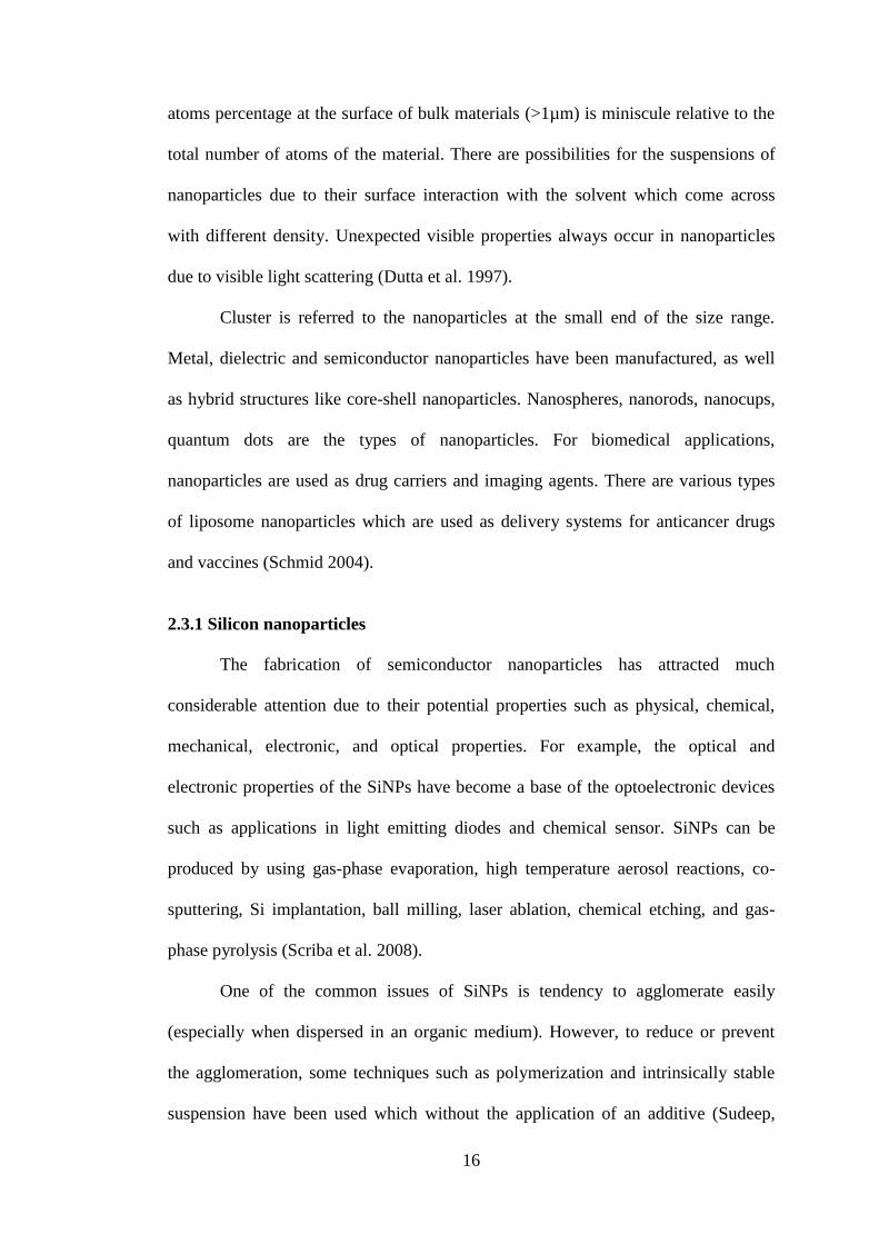
Page & Emrick 2008; Reindl & Peukert 2008). Figure 2.2 shows a transmission
electron microscope (TEM) image of SiNPs.
Figure 2.2: TEM image of SiNPs (Meier et al. 2006).
2.4 Properties of silicon nanoparticles
2.4.1 Structural properties
If compare to “bulk” structure, the structure of SiNPs is more flexible due to
its small size and large surface-to-volume ratio. This results in significant difference
to the bulk material, which is the distribution of atoms over different lattice sites
(Fang, Weng & Ju 2009).
For example, when the magnitude of the applied strain increases from 0.067
to 0.086, the amorphous phase cone of the SiNPs disappear and the surface regions
begin to transform into an amorphous state. This transformation phenomenon is quite
different in silicon bulk material as the particle microstructure reconstructs to a more
stable form (Fang, Weng & Ju 2009).
18
Besides, due to the flexibility of the nanoparticles crystal structure,
nanoparticles chemical composition can allow large compositional deviations from
the bulk stoichiometry without losing the single-phase structure. The different
crystallinity state of nanoparticles is depending on the synthesis methods in used
(Makovec 2007).
2.4.2 Mechanical properties
Mechanical properties of the materials such as hardness, elastic modulus,
fracture toughness, scratch resistance, fatigue strength, and hardness are modified
due to the nanosized of materials. At the nanoscale, structuring components have
been influenced by the energy dissipation, mechanical coupling within arrays of
components, and mechanical nonlinearities. Besides, the mechanical properties of
materials at the nanoscale always differ with the materials at macroscopic scale.
Although the continuum mechanics are applied, the surface effects can be controlled
by the deformation of properties when the sizes of materials are above the 10nm
range. Meanwhile, for micrometer sizes structures, the elastic strain energy is used to
by the deformation of properties when the size of material is above 10nm range.
Meanwhile, for micrometer sizes structures, the elastic strain energy is used to
control the mechanical properties. At nanoscale, surface effects become predominant
and significantly modify the macroscopic properties due to the increment of surface-
to-volume ratio (Cuenot et al. 2004).
For example, stress value of SiNPs which approximately 24GPa is higher
than bulk silicon (12GPa). This is because of the suppression of the dislocations in
the current small volume particles. Besides, SiNPs have a higher maximum strength
and hardness than the bulk silicon (Gerberich et al. 2003). In addition, Young‟s
moduli of SiNPs are significantly higher than bulk silicon due to the different
19
structure of the nanoscale particles from the bulk silicon (Fang, Weng & Ju 2009).
However, when the volume of the particle is reduced, smaller particles will reduce
the maximum strength significantly.
2.4.3 Optical properties
There is much significance for the optical properties of nanoparticles in both
traditional and emerging technologies. For the traditional technologies, nanoparticles
are used as coloring agents in glass and paints. In the 1970s, nanoparticle optics
researches were developed frequently due to the increased of solar-energy
applications interest. Today, nanoparticles are used to absorb at particular solar
wavelengths (commercial coatings). Due to the increment and enhancement of local
fields close to particle surfaces, nanoparticles are used to detect single molecules by
using surface-enhanced spectroscopy.
The origin colour of nanomaterials is known as surface plasmons, which is a
natural oscillation of the electron gas inside a given nanosphere. The surface
plasmons will absorb energy if the sphere is smaller compare to a wavelength of light
which has a frequency close to the surface plasmons. Besides that, the dielectrics
function and the shape of the nanoparticles may influence the frequency of the
surface plasmons (Pinchuk 2005).
Optical emission and absorption depend on the transitions between these
states; in particular, there are large changes in optical properties that are shown by
semiconductors and metals, which the colour as a function of particle size. For
example, SiNPs colloidal solutions have a colorless but become dark grey color
when particles size is increased (Sudeep, Page & Emrick 2008).
Normally, due to the intensity of absorption or transmittance, the optical
properties of SiNPs are characterized by UV-vis spectroscopy. For example, the
20
large blue shift in the absorption spectra of the SiNPs are corresponding to quantum
confinement effects on the SiNPs (Sudeep, Page & Emrick 2008; Aihara et al. 2001).
However, due to the quantum confinement effects, the red shift in the absorption
spectra of SiNPs occurred with increasing of particles size. The size-dependent
optical absorption observation is the quantum confinement signature (Brus 1994). In
addition, the surface defects of the nanoparticles also play an important role in the
absorption spectra for SiNPs (Zou et al. 2006). Besides, the shifting of SiNPs
absorption spectra could be formed from the oxidation of silicon surface due to the
incomplete or complete surface coverage (Scriba et al. 2008; Gupta & Wiggers 2009).
For the SiNPs with polymer coating, the effect depends on the thickness of polymer
coating (Blummel et al. 2007).
2.4.4 Electronic/electrical properties
In macroscopic systems, scattering at rough interfaces or scattering with
phonons, impurities or other carriers can be determined by the electronic transport.
Each electron path resembles a random walk and transport is diffusive. Electrons can
travel through the system without the phase randomization when dimensions of the
system are smaller than the electron means free path (inelastic scattering). This gives
rise to additional localization phenomena which are specifically related to phase
interference. All scattering centers can be eliminated completely if the system is
sufficiently small. Meanwhile, if the sample boundaries are smooth, boundary
reflections will be purely specular and the electron transport becomes purely ballistic,
which the sample acts as a wavelength for the electron wavefunction (Cao 2004).
However, surface modification has been changed in electrical conductivity of
the particles. The electrical conductivity of pure and modified particles is totally
different. Due to the deprotonation of hydroxyl groups, the surface of pure and
21
modified particles is negatively charged. By the way, the electric conductivity is
lower for the modified particles than pure particles which polymer (such as PEG and
PPG) grafted on the modified particles surface is non-conductive (Shin et al, 2008).
2.4.5 Thermal properties
The properties of the silicon nanomaterials such as optical, electronic and
mechanical properties have been well developed. However, the thermal properties of
nanomaterials have only shown slower progression because of the difficulties in
experimental measuring and controlling the thermal transport in nanoscale
dimensions. Moreover, the theoretical simulations and analysis of thermal transport
in nanostructures are still in infancy due to the limitation of the available approaches
(numerical solutions of Fourier‟s law, computational calculation based on Boltzmann
transport equation and Molecular-dynamics (MD) simulation). On the other hand,
Atomic force microscope (AFM) with nanometer-scale high spatial resolution is an
effective way to measure the thermal properties such as measuring the nanostructures
of thermal transport (Cao 2004).
2.4.6 Thermodynamic properties
Thermodynamic properties of SiNPs are corresponded to the cohesive energy
and the surface energy. It reveals that negative cohesive energy of the particles
increasing when the particle size increases. That means that the stability of the
particles can be improved as particles become larger. When the small particles have
more suspension bond and activation energy, the atoms on the particle‟s surface will
be reconstructed to be a more stable structure. Subsequently, when the particles size
increases, it can attribute to the surface/volume ratio. Besides, surface energy of
22
silicon nanoparticles increases significantly when the particles decreases, which
smaller particles have a higher chemical activity (Fang, Weng & Ju 2009).
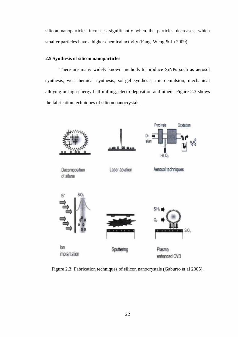
2.5 Synthesis of silicon nanoparticles
There are many widely known methods to produce SiNPs such as aerosol
synthesis, wet chemical synthesis, sol-gel synthesis, microemulsion, mechanical
alloying or high-energy ball milling, electrodeposition and others. Figure 2.3 shows
the fabrication techniques of silicon nanocrystals.
Figure 2.3: Fabrication techniques of silicon nanocrystals (Gaburro et al 2005).
23
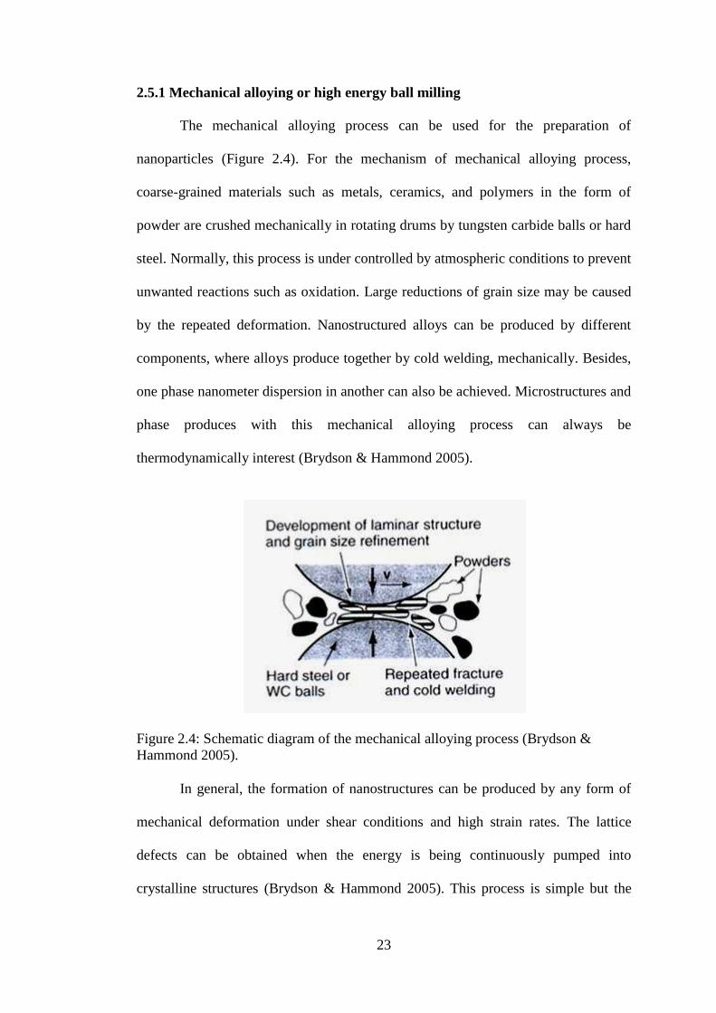
2.5.1 Mechanical alloying or high energy ball milling
The mechanical alloying process can be used for the preparation of
nanoparticles (Figure 2.4). For the mechanism of mechanical alloying process,
coarse-grained materials such as metals, ceramics, and polymers in the form of
powder are crushed mechanically in rotating drums by tungsten carbide balls or hard
steel. Normally, this process is under controlled by atmospheric conditions to prevent
unwanted reactions such as oxidation. Large reductions of grain size may be caused
by the repeated deformation. Nanostructured alloys can be produced by different
components, where alloys produce together by cold welding, mechanically. Besides,
one phase nanometer dispersion in another can also be achieved. Microstructures and
phase produces with this mechanical alloying process can always be
thermodynamically interest (Brydson & Hammond 2005).
Figure 2.4: Schematic diagram of the mechanical alloying process (Brydson &
Hammond 2005).
In general, the formation of nanostructures can be produced by any form of
mechanical deformation under shear conditions and high strain rates. The lattice
defects can be obtained when the energy is being continuously pumped into
crystalline structures (Brydson & Hammond 2005). This process is simple but the
24
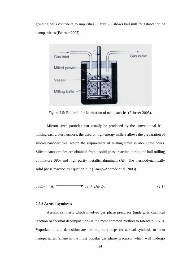
grinding balls contribute to impurities. Figure 2.5 shows ball mill for fabrication of
nanoparticles (Fahrner 2005).
Figure 2.5: Ball mill for fabrication of nanoparticles (Fahrner 2005).
Micron sized particles can usually be produced by the conventional ball-
milling easily. Furthermore, the used of high-energy millers allows the preparation of
silicon nanoparticles, which the requirement of milling times is about few hours.
Silicon nanoparticles are obtained from a solid phase reaction during the ball milling
of mixture SiO2 and high purity metallic aluminum (Al). The thermodynamically
solid phase reaction as Equation 2.1: (Araujo-Andrade et al. 2003).
3SiO2 + 4Al 3Si + 2Al2O3 (2.1)
2.5.2 Aerosol synthesis
Aerosol synthesis which involves gas phase precursor (undergoes chemical
reaction or thermal decomposition) is the most common method to fabricate SiNPs.
Vaporization and deposition are the important steps for aerosol synthesis to form
nanoparticles. Silane is the most popular gas phase precursor which will undergo
25
pyrolysis to produce SiNPs. Due to the configuration set up, there are various types
of aerosol synthesis to produce nanoparticles.
Advantages of the gas-phase processing systems are shown as follows:-
The purity of nanoparticles which produce by gas-phase processes is
generally higher than liquid-based processes.
Aerosol synthesis provides a good process and product control because of
particle size, degree of agglomeration, chemical homogeneity, and
crystallinity can be controlled easily.
Aerosol synthesis being a non-vacuum technique which provides a cheap
alternative rather than expensive vacuum synthesis technique for synthesis of
thin or thick film (Wang, Zhong & Snyder 1990).
i) Laser vaporization
A laser is used to evaporate a sample target in an inert gas flow reactor.
Vaporization is caused by laser which has heated the source material to a high
temperature, locally. Supersaturation occurs when the vapor is cooled by collisions
with the inert gas molecules. Nanoparticles formation is induced by the
supersaturation. For example, CO2 laser is used to induce pyrolysis of silane.
Meanwhile, it produces gram-scale quantities of SiNPs. High purity loosely
agglomerated particles with controlled primary particle size and size distribution can
also be produced by CO2 laser (Li et al 2003).
ii) Pulsed laser ablation
Pulsed laser ablation is one of the most common used deposition methods in
preparing nanocrystalline silicon films due to the rapid thermogenic speed and small
surface contamination (Wang et al. 2006). Energetic plasma above a thin layer of