light spectral filtering based on spatial adiabatic passage
TRANSCRIPT

ORIGINAL ARTICLE
Light spectral filtering based on spatial adiabatic passage
Ricard Menchon-Enrich1, Andreu Llobera2, Jordi Vila-Planas2, Vıctor J Cadarso3, Jordi Mompart1
and Veronica Ahufinger1
We present the first experimental realization of a light spectral filter based on the spatial adiabatic passage technique. We demonstrate
that a fully integrable CMOS-compatible system of three coupled identical total internal reflection silicon oxide waveguides with
variable separation along their propagation direction can be used simultaneously as a low- and high-pass spectral filter within the
visible range of wavelengths. Light is injected into the right waveguide, and after propagating along the system, long wavelengths are
transferred into the left output, whereas short wavelengths propagate to the right and central outputs. The stopband reaches values up
to 211 dB for the left output and approximately 220 dB for the right plus central outputs. The passband values are close to 0 dB for
both cases. We also demonstrate that the filtering characteristics of the device can be controlled by modifying the parameter values,
which define the geometry of the triple-waveguide system. However, the general filtering behavior of the system does not critically
depend on technological variations. Thus, the spatial adiabatic passage filtering approach constitutes an alternative to other integrated
filtering devices, such as interference or absorbance-based filters.
Light: Science & Applications (2013) 2, e90; doi:10.1038/lsa.2013.46; published online 16 August 2013
Keywords: CMOS-compatible technology; integrated optics devices; spatial adiabatic passage; wavelength filtering devices
INTRODUCTION
Photonic integrated circuits (PICs) have the potential to revolutionize
computing platforms due to the high speed and quality of light-based
communications. Recently, photonic integration has been pushed
forward by taking advantage of complementary metal-oxide-semi-
conductor (CMOS)-compatible technology, which allows high quality
PICs to be obtained with high-index contrasts.1,2 Due to this contrast,
sharp bends can be implemented, leading to significant miniaturiza-
tion of the optical components. Furthermore, CMOS-compatibility
allows the usage of already developed mass-production fabrication
techniques for electronic components on the one hand and the mono-
lithic integration of PICs with additional electronic circuits on the
other hand. In this context, several research groups have successfully
characterized silicon-based PICs, such as couplers, power splitters,
optical modulators, wavelength demultiplexers (WDMs) and fil-
ters.3–6 Among them, the structures able to perform wavelength filter-
ing have attracted significant interest mainly due to their potential to
be applied not only in telecommunication applications, but also in
other fields, such as spectroscopy7 or sensing.8
Different strategies and geometries toward implementing all-
optical integrated PICs for filtering have been previously presented.
Several types of interference-based integrable spectral filters have been
proposed. First are structures that are commonly called single chan-
nels, with the most representative being ring resonators8 and Mach–
Zehnder interferometers.9 Second, a more advanced configuration
uses multiple channels or WDMs, in which the current trends are
arrayed waveguide gratings10 and planar concave gratings (also known
as echelle gratings).11 With respect to ring resonators, high Q values
are obtained due to the strong field enhancement caused by recursive
light propagation inside the structure. This feedback, however, also
causes nonlinearities, which distort the device response. Regarding
Mach–Zehnder interferometers, the main open issue is related to
the critical coupling ratio between the stages, which basically depends
on the critical technological steps, as well as the matching between the
delay lengths. In the case of WDMs, planar concave gratings have the
advantage of a minor footprint; however, in arrayed waveguide grat-
ings, it is possible to selectively tune each delay line and, in general,
there is significantly larger design freedom. Nevertheless, in both cases,
the required technology is critical, and the robustness against tech-
nological variations is very low. The shallow etch configuration12 par-
tially solves this issue, but at the expense of requiring an additional and
highly accurate photolithographic step, and still demands highly pre-
cise etching steps. In this context, spectral filtering structures based on
both single and multiple channels require an extremely robust
technology that uses both critical alignment and etching steps.
Nevertheless, they are undoubtedly the workhorse of telecommuni-
cation applications. It is also true that such strict technological steps
clearly hamper their applications where instead of narrow and sharp
peaks, robustness and technological simplicity are key issues.
Absorbance-based integrated filters offer an alternative.13 Typically,
their stopband and passband extend to a broad region instead of pre-
senting single/multiple peaks, and absorbance-based integrated filters
are easy to implement and characterize. However, the difference
between the passband and stopband is not as high when compared
1Department of Physics, Universitat Autonoma de Barcelona, E-08193 Bellaterra, Barcelona, Spain; 2Chemical Transducers Group, Institut de Microelectronica de Barcelona (IMB-CNM, CSIC), E-08193 Bellaterra, Barcelona, Spain and 3Microsystems Laboratory (LMIS1), Ecole Polytechnique Federale de Lausanne (EPFL), CH-1015 Lausanne, SwitzerlandCorrespondence: R Menchon-Enrich, Department of Physics, Universitat Autonoma de Barcelona, E-08193 Bellaterra, Barcelona, SpainE-mail: [email protected]
Received 26 October 2012; revised 23 January 2013; accepted 28 January 2013
Light: Science & Applications (2013) 2, e90; doi:10.1038/lsa.2013.46� 2013 CIOMP. All rights reserved 2047-7538/13
www.nature.com/lsa

to that of interference filters, and the spectral filtering cannot be tuned
because it depends either on the particular organic compound14 or on
the bandgap material in the filter.15
In this article, we introduce a completely new method of light spec-
tral filtering, based on the so-called adiabatic passage of light tech-
nique.16–18 We experimentally demonstrate that a system of three
identical total internal reflection (TIR) silicon oxide coupled wave-
guides can act simultaneously as a high- and low-pass spectral filter for
the visible range, separating the long and short wavelengths among the
different waveguides. We will refer to this type of filter as a spatial
adiabatic passage (SAP) filter. The proposed configuration shows a
different filtering behavior compared to interference filters,12 because
there is an absence of periodic peaks but a wide transmission band,
while maintaining a moderate difference between the passband and
stopband values. Moreover, in contrast to absorbance-based filters,13
the filtering characteristics of the SAP filter can be modified by varying
the geometric parameters of the structure. However, variations in a
given geometrical parameter value do not imply a severe change in the
spectral response. Therefore, in contrast to the interference filters, the
SAP filters proposed here have high technological robustness.
Additionally, the SAP triple-waveguide system is fully CMOS-com-
patible and technologically simple to fabricate, requiring only one,
non-critical photolithographic step. As such, SAP filters can be mono-
lithically implemented with other electronic elements into photonic
integrated circuits with a low-cost and mass-production.
MATERIALS AND METHODS
The propagation of light into a system of three identical single-mode
evanescent coupled waveguides can be described through coupled
mode equations.19,20 These equations govern the evolution of the ai
amplitude functions that correspond to the fundamental mode of each
i waveguide along the z propagation direction, where i~L,C,R
accounts for the left, central and right waveguides, respectively:
id
dz
aR
aC
aL
0B@
1CA~
0 VR(z,l) 0
VR(z,l) 0 VL(z,l)
0 VL(z,l) 0
0B@
1CA
aR
aC
aL
0B@
1CA ð1Þ
whereVR (VL) is the coupling coefficient between the central and right
(left) waveguides. Because weak coupling is assumed, the right and left
waveguides are not directly coupled.
Diagonalizing Equation (1), it can be seen that one of the eigenvec-
tors of the system (supermode) only involves light in the right and left
waveguides:
D(H)~
cosH
0
{sinH
0B@
1CA ð2Þ
with tanH:VR=VL. Because the couplings are due to the evanescent
fields, they can be easily modified by engineering the transverse
waveguide separation along the z propagation direction. In particular,
we consider the right waveguide of the SAP filter to be excited by the
input light source, and the spatial configuration of the waveguides
forces the couplings to follow a counterintuitive sequence along z.
Initially, the left waveguide approaches the central waveguide. Later,
and with a certain overlap, the right waveguide approaches the central
waveguide, whereas the left waveguide separates from the central
waveguide, as shown in Figure 1a. With this spatial configuration,
the mixing angle, H, evolves from 0 to p=2. If the modification of H
is adiabatically performed, the supermode (2) is followed, and light
x
x
z
x0
x0
y
L C R
1.5 μm0.5 μm
4 μm
SiOy
SiOx
SiO2
Si 3.821.461.481.46Refractive indices
2 μm
2 μm
zδ
a b
Figure 1 (a) A schematic depiction of the SAP filter geometry, viewed from above, consisting of one straight central waveguide (C) and two circularly bent external
waveguides, right (R) and left (L). The z separation between the centers of the bent waveguides is given by d, and the minimum separation between waveguides is
defined by x0. The device’s total length in the z direction is D52.5 cm and the external waveguides’ radius of curvature is r53.5 m. (b) A schematic representation of the
different layers of one of the rib waveguides, specifying the refractive indices and materials.
Light spectral filtering based on spatial adiabatic passage
R Menchon-Enrich et al
2
Light: Science & Applications doi:10.1038/lsa.2013.46
will be efficiently transferred between the outermost waveguides (from
right to left in our case) without the propagation of light intensity into
the central waveguide.
We also can understand this process by showing the evolution along
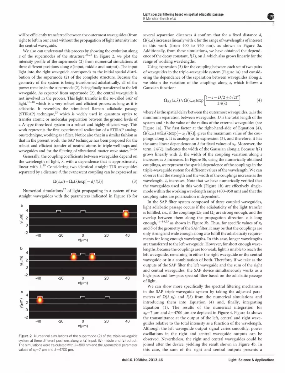
z of the supermodes of the structure.21,22 In Figure 2, we plot the
intensity profile of the supermode (2) from numerical simulations at
three different positions along z (input, middle and output). The input
light into the right waveguide corresponds to the initial spatial distri-
bution of the supermode (2) of the complete structure. Because the
geometry of the system is being transformed adiabatically, all of the
power remains in the supermode (2), being finally transferred to the left
waveguide. As expected from supermode (2), the central waveguide is
not involved in the process. This light transfer is the so-called SAP of
light,16–18 which is a very robust and efficient process as long as it is
adiabatic. It resembles the stimulated Raman adiabatic passage
(STIRAP) technique,23 which is widely used in quantum optics to
transfer atomic or molecular population between the ground levels of
a L-type three-level system in a robust and highly efficient way. This
work represents the first experimental realization of a STIRAP analog-
ous technique, working as a filter. Notice also that in a similar fashion as
that in the present work, the SAP technique has been proposed for the
robust and efficient transfer of neutral atoms in triple-well traps and
waveguides and for the filtering of vibrational matter wave states.24–26
Generally, the coupling coefficients between waveguides depend on
the wavelength of light, l, with a dependence that is approximately
linear with l.19 Considering two identical straight TIR waveguides
separated by a distance d, the evanescent coupling can be expressed as:
V(l,d)~V0(l)exp {d=l(l)½ � ð3Þ
Numerical simulations27 of light propagating in a system of two
straight waveguides with the parameters indicated in Figure 1b for
several separation distances d confirm that for a fixed distance d,
V(l,d) increases linearly with l for the range of wavelengths of interest
in this work (from 400 to 950 nm), as shown in Figure 3a.
Additionally, from these simulations, we have obtained the depend-
ence of the decay constant, l(l), on l, which also grows linearly for the
range of working wavelengths.
Using expression (3) for the coupling between each set of two pairs
of waveguides in the triple-waveguide system (Figure 1a) and consid-
ering the dependence of the separation between waveguides along z,
we obtain the variation of the couplings along z, which follows a
Gaussian function:
VR,L(z,l)&V(l,x0)exp({z{D=2+d=2)2
2rl(l)
� �ð4Þ
where d is the spatial delay between the outermost waveguides, x0 is the
minimum separation between waveguides, D is the total length of the
system and r is the value of the radius of the external waveguides (see
Figure 1a). The first factor at the right-hand-side of Equation (4),
V(l,x0):V0(l)exp {x0=l(l)½ �, gives the maximum value of the cou-
plings along z. It is analogous to expression (3), and therefore, it has
the same linear dependence on l for fixed values of x0. Moreover, the
term, 2rl(l), indicates the width of the Gaussian along z. Because l(l)
grows linearly with l, the width of the coupling variation along z
increases as l increases. In Figure 3b, using the numerically obtained
couplings, we represent the spatial dependence of the couplings in the
triple-waveguide system for different values of the wavelength. We can
observe that the strength and the width of the couplings increase as the
wavelength, l, increases. Note that we have numerically verified that
the waveguides used in this work (Figure 1b) are effectively single-
mode within the working wavelength range (400–950 nm) and that the
coupling rates are polarization independent.
In the SAP filter system composed of three coupled waveguides,
light adiabatic passage occurs if the adiabaticity of the light transfer
is fulfilled, i.e., if the couplings VR and VL are strong enough, and the
overlap between them along the propagation direction z is long
enough,16–18,23 as shown in Figure 3b. Thus, for specific values of x0
and d of the geometry of the SAP filter, it may be that the couplings are
only strong and wide enough along z to fulfill the adiabaticity require-
ments for long enough wavelengths. In this case, longer wavelengths
are transferred to the left waveguide. However, for short enough wave-
lengths, because the couplings are too weak, light is unable to reach the
left waveguide, remaining in either the right waveguide or the central
waveguide or in a combination of both. Therefore, if we take as the
outputs of the SAP filter the left waveguide and the sum of the right
and central waveguides, the SAP device simultaneously works as a
high-pass and low-pass spectral filter based on the adiabatic passage
of light.
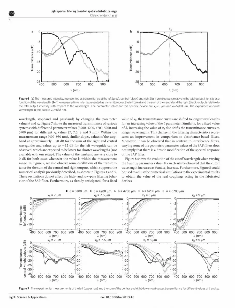
We can show more specifically the spectral filtering mechanism
in the SAP triple-waveguide system by taking the adjusted para-
meters of V(l,x0) and l(l) from the numerical simulations and
introducing them into Equation (4) and, finally, integrating
Equation (1). The results of the numerical integration for
x057 mm and d54700 mm are depicted in Figure 4. Figure 4a shows
the transmittance at the output of the left, central and right wave-
guides relative to the total intensity as a function of the wavelength.
Although the left waveguide output signal varies smoothly, power
oscillations in the right and central waveguide outputs can be
observed. Nevertheless, the right and central waveguides could be
joined after the device, yielding the result shown in Figure 4b. In
this case, the sum of the right and central outputs presents a
2
-2-40 -20 0
x(mm)
y(mm
)
20 40
-40 -20 0x(mm)
20 40
-40 -20 0x(mm)
20 40
0
4
2
-2
y(mm
)
0
4
2
-2
y(mm
)
0
4
a
b
c
Figure 2 Numerical simulations of the supermode (2) of the triple-waveguide
system at three different positions along z: (a) input, (b) middle and (c) output.
The simulations were calculated with l5800 nm and the geometrical parameter
values of x057 mm and d54700 mm.
Light spectral filtering based on spatial adiabatic passageR Menchon-Enrich et al
3
doi:10.1038/lsa.2013.46 Light: Science & Applications
significantly more robust behavior, and we can observe the pre-
dicted behavior of the SAP filter which works simultaneously as a
high-pass and low-pass spectral filter. In particular, within the range
of studied wavelengths, for the left waveguide (high-pass), we find a
stopband that reaches a value of 217 dB and a passband of 0 dB. For
the sum of the right and central waveguide intensities (low-pass), we
find a stopband that reaches 222 dB and a passband of 0 dB. Taking
into account that the device can work as a high- and low-pass spectral
filter simultaneously, we define the cutoff wavelength, lc , as the wave-
length for which half of the intensity is at the output of the left
waveguide and half at the output of the other two waveguides.
Thus, lc corresponds to a decrease in intensity of approximately
3 dB and to the point at which the two curves in Figure 4 cross each
other. For the presented figure, the cutoff wavelength is 610 nm.
Since SAP filtering is based on the robust technique of the adiabatic
passage of light, we expect a similar filtering behaviour, even though
the geometric parameter values of the system are significantly modi-
fied. Nevertheless, studying the effect of varying the x0 and d para-
meters, we can observe that the specific filtering characteristics of the
device (the cutoff wavelength, as well as the stop and passband
regions) can be tuned by wavelength. On the one hand, if the spatial
delay value d is increased, the overlap between the couplings becomes
smaller. Thus, only strong and wide enough couplings along z will
fulfill the adiabaticity condition. On the other hand, if the minimum
separation between the waveguides x0 is increased, the strength of the
couplings will be reduced, because the coupling values decay expo-
nentially as the distance between the waveguides increases. Then,
stronger and wider couplings (corresponding to long wavelengths)
will also be required to maintain the adiabaticity of the process. In
conclusion, the filtering characteristics, such as the cutoff wavelength,
are moved to longer wavelengths as the values of x0 and d increase. The
numerical simulations integrating Equation (1) with the adjusted
parameters V(l,x0) and l(l) support this reasoning, as it can be
observed in Figure 5.
Numerical simulations were performed to optimize the geometry of
the triple-waveguide SAP filter for different wavelengths27 such that
the obtained parameter values were used to define the required tech-
nological steps. The SAP filters were fabricated with a total length of
1.6d = 7 µmd = 7.5 µmd = 8 µm
d = 9 µmd = 10 µm
d = 8.5 µm
1.4
1.2
1.0
0.8
Ω(l
,d) (
mm
-1)
0.6
0.4
0.2
0.0
1.2
1.0
0.8
ΩR,L
(mm
-1)
0.6
0.4
0.2
0.00 5 10
z (mm)15 20 25
400 500 600 700
l (nm)
800 900 1000
ΩL ΩR
da b
Figure 3 Numerical simulations for the characterization of the couplings. (a) The dependence of the coupling coefficient between two straight TIR waveguides (with
the characteristics specified in Figure 1b), V(l,d), on l for fixed distances d. The simulation points are fitted by straight lines. (b) The typical counterintuitive sequence
of coupling coefficients along z in a system of three coupled waveguides obtained from numerical simulations27 with x057 mm and d54700 mm for different
wavelengths, including 400 nm (dotted), 600 nm (dashed) and 800 nm (solid). The increase in the strength and width of the couplings along the z direction can
be observed as the wavelength l increases.
0
-10
-20
-30
-40
-50400
0
-10
-20
-30
-40
-50400600
Tran
smitt
ance
(dB
)
Tran
smitt
ance
(dB
)
Left waveguideCentral waveguide Left waveguide
Central + right waveguidesRight waveguide
800 1000 1200 600 800 1000 1200
l (nm) l (nm)
lca b
Figure 4 The results of the numerical integration of Equation (1) with parameter values x057 mm and d54700 mm. (a) The transmittance at the output of the left
(dashed line), central (dashed-dotted line) and right (solid line) waveguides, represented relative to the total output intensity as a function of the wavelength. In (b), the
high- and low-pass filtering behavior for a SAP filter can be observed, represented as the transmittance at the output of the left (dashed line) and the sum of the central
and the right (solid line) waveguides relative to the total output intensity with respect to the wavelength. No losses are considered when integrating Equation (1).
Light spectral filtering based on spatial adiabatic passage
R Menchon-Enrich et al
4
Light: Science & Applications doi:10.1038/lsa.2013.46

2.5 cm, and external waveguides were given a radius of curvature of
3.5 m. To obtain devices with different filtering characteristics, for
every system of waveguides, slightly different parameter values of
the spatial delay d and minimum separation between waveguides x0
also were fabricated.
The fabrication process for the triple-waveguide systems includes
the following stages. Initially, a 2-mm-thick layer of SiO2 was thermally
grown on a (100) silicon wafer. After that, a layer of non-stoichi-
ometric silicon oxide SiOx with a refractive index of 1.48 and a height
of 2 mm was deposited by plasma-enhanced chemical vapor depos-
ition.28 At this stage, ribs of 4mm width and a thickness of 0.5mm in the
SiOx layer were defined by using the previously designed mask and dry
etching, and the waveguides were obtained. Finally, a 2-mm-thick
passivation layer of non-stoichiometric silicon oxide SiOy with
refractive index 1.46 was deposited using plasma-enhanced chemical
vapor deposition. Figure 1b shows the transverse profile of a wave-
guide belonging to the triple-waveguide system, specifying the sizes of
the layers and the refractive index values, which were measured by
ellipsometry.28
The experimental setup is composed of a halogen white light source
(Ocean Optics HL-2000-HP-FHSA, Dunedin, Florida, USA) con-
nected to a 4-mm core optical fiber (Thorlabs 600HP, Newton, New
Jersey, USA). The position of the other end of the fiber is controlled by
a piezoelectric three-dimensional positioning system (Piezosystem
Jena NV40/3, Jena, Germany), which provides nanometer-scale pre-
cision alignment between the optical fiber and the waveguide. The
light emerging from the system is collected by another 4-mm core
optical fiber, placed on another piezoelectric positioning system
(Piezosystem Jena d-Drive) and transmitted to a microspectrometer
(Ocean Optics QE65000).
With respect to the losses of the SAP filter, since the final goal of our
proposal is to place the device into a PIC, we are mainly interested in
the losses produced by the SAP geometry of the system, i.e., those
losses due to the couplings and the bending of the waveguides, but
not in the insertion and propagation losses, which depend on the
characteristics of the specific waveguides. Thus, we studied the losses
due to the adiabatic passage geometry by comparing the sum of the
output intensities of the three waveguides of the device with the output
of a single straight waveguide with equal features and the same length
as the system of three waveguides. The experimental and numerical
tests show that the losses due to the adiabatic passage geometry are
negligible. With respect to the range of wavelengths available in the
presented experimental setup, 400–950 nm can be sampled. The range
is mainly limited by the allowed wavelengths propagating inside the
fibers in addition to the sensitivity of the microspectrometer.
RESULTS AND DISCUSSION
The result shown in Figure 6 experimentally demonstrates the spectral
filtering, based on the adiabatic passage of light technique for one of
the fabricated SAP filters with a minimum separation between wave-
guides of x059 mm and a spatial delay of d55200 mm. Figure 6a shows
the intensity at the output of the left, central and right waveguides as
transmittance relative to the total output intensity (we previously
verified that the losses due to the adiabatic passage geometry are neg-
ligible). As expected from the numerical simulations, some power
oscillations can be observed between the right and central waveguides,
depending on the wavelength. However, we could join the right and
central waveguides in a single waveguide just after the described triple-
waveguide system by appropriately designing the photomask used for
fabrication. By doing this, we would obtain an output corresponding
to the sum of the right and central waveguides, which presents a
significantly smoother and more robust behavior, as obtained from
the numerical simulations. Thus, Figure 6b represents the experiment-
ally measured intensity at the output of the left waveguide and the sum
of the outputs of the right and central waveguides as the transmittance
relative to the total output intensity.
From this result, we experimentally conclude that the triple-wave-
guide SAP filter acts as a high-pass (output at the left waveguide) and
low-pass (output at the central and right waveguides) spectral filter,
representing a new and different filtering behavior in comparison to
interference filters12 and absorbance-based filters.13 We have obtained
a filtering efficiency between the efficiency of the inteference and the
absorbance-based filters. In particular, the measured values for the left
waveguide output (high-pass) reach a value of approximately 211 dB
for the stopband, and the passband is close to 0 dB. For the sum of right
and central (low-pass) waveguides, the stopband is approximately
220 dB and the passband 20.5 dB. The measured cutoff wavelength
is 638 nm.
As discussed in the ‘Materials and methods’ section, SAP filters
allow for a modification of the filtering characteristics (the cutoff
0
-10
-20
-30
-40
-50400 600 800 1000 1200
l (nm)
0
-10
-20
-30
-40
-50400 600 800 1000 1200
l (nm)
Left waveguideCentral + right waveguides
Left waveguideCentral + right waveguides
lclcba
Tran
smitt
ance
(dB
)
Tran
smitt
ance
(dB
)
Figure 5 The numerical simulations of the high- and low-pass spectral filtering behavior for a SAP filter with (a) x057 mm and d55700 mm and (b) x059 mm and
d54700 mm. In comparison with the curves in Figure 4 with x057 mm and d54700 mm (light grey in these figures), we observe that when increasing the value of (a) d
and (b) x0, the cutoff wavelength of the device is moved to longer wavelengths. In all cases, the output of the left (central and right) waveguides corresponds to the
dashed (solid) line.
Light spectral filtering based on spatial adiabatic passageR Menchon-Enrich et al
5
doi:10.1038/lsa.2013.46 Light: Science & Applications
wavelength, stopband and passband) by changing the parameter
values d and x0. Figure 7 shows the measured transmittance of various
systems with different d parameter values (3700, 4200, 4700, 5200 and
5700 mm) for different x0 values (7, 7.5, 8 and 9 mm). Within the
measurement range (400–950 nm), similar slopes, values of the stop-
band at approximately 220 dB for the sum of the right and central
waveguides and values up to 212 dB for the left waveguide can be
observed, which are expected to be lower for shorter wavelengths (not
available with our setup). The values of the passband are very close to
0 dB for both cases whenever the value is within the measurement
range. In Figure 7, we also observe some oscillations of the transmit-
tance for the sum of the central and right outputs, which supports the
numerical analysis previously described, as shown in Figures 4 and 5.
These oscillations do not affect the high- and low-pass filtering beha-
vior of the SAP filter. Furthermore, as already anticipated, for a fixed
value of x0, the transmittance curves are shifted to longer wavelengths
for an increasing value of the d parameter. Similarly, for a fixed value
of d, increasing the value of x0 also shifts the transmittance curves to
longer wavelengths. This change in the filtering characteristics repre-
sents an improvement in comparison to absorbance-based filters.
Moreover, it can be observed that in contrast to interference filters,
varying some of the geometric parameter values of the SAP filters does
not imply that there is a drastic modification of the spectral response
of the SAP filter.
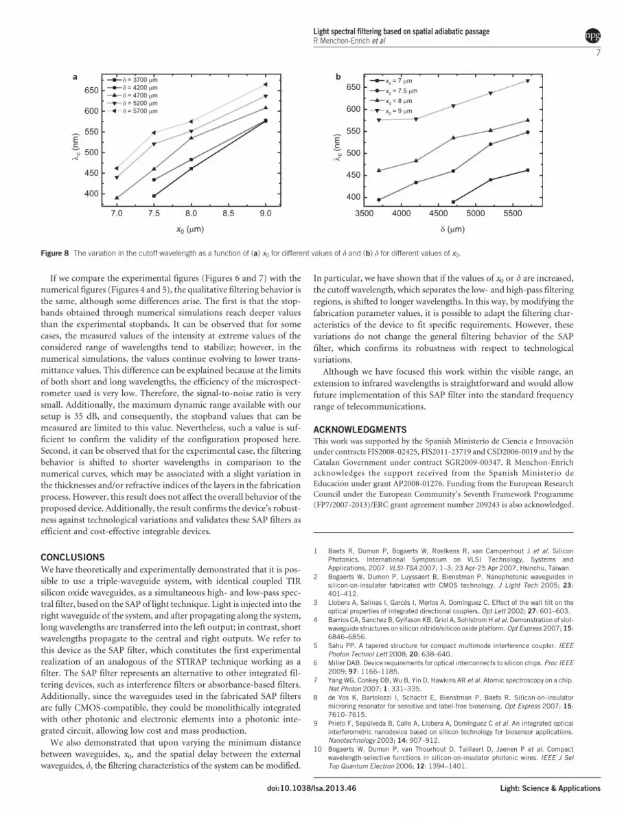
Figure 8 shows the evolution of the cutoff wavelength when varying
the d and x0 parameter values. It can clearly be observed that the cutoff
wavelength increases as d and x0 increase. Furthermore, Figure 8 could
be used to adjust the numerical simulations to the experimental results
to obtain the value of the real couplings acting in the fabricated
devices.
0
-5
-10
-15
-20
-25400 500
Tran
smitt
ance
(dB
)
600 700 800 900
l (nm)
a 0
-5
-10
-15
-20
-25400 500
Tran
smitt
ance
(dB
)
600 700 800 900
l (nm)
blc
Figure 6 (a) The measured intensity, represented as transmittance at the left (grey), central (black) and right (light grey) outputs relative to the total output intensity as a
function of the wavelength. (b) The measured intensity, represented as transmittance at the left (grey) and the sum of the central and the right (black) outputs relative to
the total output intensity with respect to the wavelength. The parameter values for this specific device are x059 mm and d55200 mm. The experimental cutoff
wavelength in this case is lc5638 nm.
0-2-4-6
Tran
smitt
ance
left
outp
ut (d
B)
Tran
smitt
ance
cent
ral +
righ
t out
puts
(dB
)
-8-10-12
-5-10-15-20-25-30-35
0-5
-10-15-20-25-30-35
0-5
-10-15-20-25-30-35
0-5
-10-15-20-25-30-35
0
400 500 600 700 800 900 400 500 600 700 800 900 400 500 600 700 800 900 400 500 600 700 800 900
0-2-4-6-8
-10-12
0-2-4-6-8
-10-12
0-2-4-6-8
-10-12
l (nm) l (nm) l (nm) l (nm)
400 500 600 700 800 900 400 500 600 700 800 900 400 500 600 700 800 900 400 500 600 700 800 900l (nm) l (nm) l (nm) l (nm)
x0 = 9 µmx0 = 8 µmx0 = 7.5 µmx0 = 7 µm
x0 = 9 µmx0 = 8 µmx0 = 7.5 µmx0 = 7 µmd = 3700 µm d = 4200 µm d = 4700 µm d = 5200 µm d = 5700 µm
Figure 7 The experimental measurements of the left (upper row) and the sum of the central and right (lower row) output transmittance for different values of d and x0.
Light spectral filtering based on spatial adiabatic passage
R Menchon-Enrich et al
6
Light: Science & Applications doi:10.1038/lsa.2013.46
If we compare the experimental figures (Figures 6 and 7) with the
numerical figures (Figures 4 and 5), the qualitative filtering behavior is
the same, although some differences arise. The first is that the stop-
bands obtained through numerical simulations reach deeper values
than the experimental stopbands. It can be observed that for some
cases, the measured values of the intensity at extreme values of the
considered range of wavelengths tend to stabilize; however, in the
numerical simulations, the values continue evolving to lower trans-
mittance values. This difference can be explained because at the limits
of both short and long wavelengths, the efficiency of the microspect-
rometer used is very low. Therefore, the signal-to-noise ratio is very
small. Additionally, the maximum dynamic range available with our
setup is 35 dB, and consequently, the stopband values that can be
measured are limited to this value. Nevertheless, such a value is suf-
ficient to confirm the validity of the configuration proposed here.
Second, it can be observed that for the experimental case, the filtering
behavior is shifted to shorter wavelengths in comparison to the
numerical curves, which may be associated with a slight variation in
the thicknesses and/or refractive indices of the layers in the fabrication
process. However, this result does not affect the overall behavior of the
proposed device. Additionally, the result confirms the device’s robust-
ness against technological variations and validates these SAP filters as
efficient and cost-effective integrable devices.
CONCLUSIONS
We have theoretically and experimentally demonstrated that it is pos-
sible to use a triple-waveguide system, with identical coupled TIR
silicon oxide waveguides, as a simultaneous high- and low-pass spec-
tral filter, based on the SAP of light technique. Light is injected into the
right waveguide of the system, and after propagating along the system,
long wavelengths are transferred into the left output; in contrast, short
wavelengths propagate to the central and right outputs. We refer to
this device as the SAP filter, which constitutes the first experimental
realization of an analogous of the STIRAP technique working as a
filter. The SAP filter represents an alternative to other integrated fil-
tering devices, such as interference filters or absorbance-based filters.
Additionally, since the waveguides used in the fabricated SAP filters
are fully CMOS-compatible, they could be monolithically integrated
with other photonic and electronic elements into a photonic inte-
grated circuit, allowing low cost and mass production.
We also demonstrated that upon varying the minimum distance
between waveguides, x0, and the spatial delay between the external
waveguides, d, the filtering characteristics of the system can be modified.
In particular, we have shown that if the values of x0 or d are increased,
the cutoff wavelength, which separates the low- and high-pass filtering
regions, is shifted to longer wavelengths. In this way, by modifying the
fabrication parameter values, it is possible to adapt the filtering char-
acteristics of the device to fit specific requirements. However, these
variations do not change the general filtering behavior of the SAP
filter, which confirms its robustness with respect to technological
variations.
Although we have focused this work within the visible range, an
extension to infrared wavelengths is straightforward and would allow
future implementation of this SAP filter into the standard frequency
range of telecommunications.
ACKNOWLEDGMENTS
This work was supported by the Spanish Ministerio de Ciencia e Innovacion
under contracts FIS2008-02425, FIS2011-23719 and CSD2006-0019 and by the
Catalan Government under contract SGR2009-00347. R Menchon-Enrich
acknowledges the support received from the Spanish Ministerio de
Educacion under grant AP2008-01276. Funding from the European Research
Council under the European Community’s Seventh Framework Programme
(FP7/2007-2013)/ERC grant agreement number 209243 is also acknowledged.
1 Baets R, Dumon P, Bogaerts W, Roelkens R, van Campenhout J et al. SiliconPhotonics. International Symposium on VLSI Technology, Systems andApplications, 2007. VLSI-TSA 2007; 1–3; 23 Apr-25 Apr 2007, Hsinchu, Taiwan.
2 Bogaerts W, Dumon P, Luyssaert B, Bienstman P. Nanophotonic waveguides insilicon-on-insulator fabricated with CMOS technology. J Light Tech 2005; 23:401–412.
3 Llobera A, Salinas I, Garces I, Merlos A, Domınguez C. Effect of the wall tilt on theoptical properties of integrated directional couplers. Opt Lett 2002; 27: 601–603.
4 Barrios CA, Sanchez B, Gylfason KB, Griol A, Sohlstrom H et al. Demonstration of slot-waveguide structures on silicon nitride/silicon oxide platform. Opt Express 2007; 15:6846–6856.
5 Sahu PP. A tapered structure for compact multimode interference coupler. IEEEPhoton Technol Lett 2008; 20: 638–640.
6 Miller DAB. Device requirements for optical interconnects to silicon chips. Proc IEEE2009; 97: 1166–1185.
7 Yang WG, Conkey DB, Wu B, Yin D, Hawkins AR et al. Atomic spectroscopy on a chip.Nat Photon 2007; 1: 331–335.
8 de Vos K, Bartolozzi I, Schacht E, Bienstman P, Baets R. Silicon-on-insulatormicroring resonator for sensitive and label-free biosensing. Opt Express 2007; 15:7610–7615.
9 Prieto F, Sepulveda B, Calle A, Llobera A, Domınguez C et al. An integrated opticalinterferometric nanodevice based on silicon technology for biosensor applications.Nanotechnology 2003; 14: 907–912.
10 Bogaerts W, Dumon P, van Thourhout D, Taillaert D, Jaenen P et al. Compactwavelength-selective functions in silicon-on-insulator photonic wires. IEEE J SelTop Quantum Electron 2006; 12: 1394–1401.
650
600
550
500
450
400
7.0 7.5 8.0 9.0 3500 4000 4500 550050008.5
l c (n
m)
650
600
550
500
450
400
l c (n
m)
x0 (µm) d (µm)
d = 3700 µm x0 = 7 µmx0 = 7.5 µmx0 = 8 µmx0 = 9 µm
d = 4200 µmd = 4700 µmd = 5200 µmd = 5700 µm
ba
Figure 8 The variation in the cutoff wavelength as a function of (a) x0 for different values of d and (b) d for different values of x0.
Light spectral filtering based on spatial adiabatic passageR Menchon-Enrich et al
7
doi:10.1038/lsa.2013.46 Light: Science & Applications
11 Brouckaert J, Bogaerts W, Dumon P, van Thourhout D, Baets R. Planar concave gratingdemultiplexer fabricated on a nanophotonic silicon-on-insulator platform. J LightwTechnol 2007; 25: 1269–1275.
12 Bogaerts W, Selvaraja SK, Dumon P, Brouckaert J, de Vos K et al. Silicon-on-insulatorspectral filters fabricated with CMOS technology. IEEE J Sel Top Quantum Electron2010; 16: 33–44.
13 Llobera A, Demming S, Joensson HN, Vila-Planas J, Andersson-Svahn H et al.Monolithic PDMS passband filters for fluorescence detection. Lab Chip 2010; 10:1987–1992.
14 Chabinyc ML, Chiu DT, McDonald JC, Stroock AD, Christian JF et al. An integratedfluorescence detection system in poly(dimethylsiloxane) for microfluidic applications.Anal Chem 2001; 73: 4491–4498.
15 Mahan AH, Biswas R, Gedvilas LM, Williamson DL, Pan BC. On the influence of shortand medium range order on the material band gap in hydrogenated amorphous silicon.J Appl Phys 2004; 96: 3818–3826.
16 Longhi S, Della Valle G, Ornigotti M, Laporta P. Coherent tunneling by adiabaticpassage in an optical waveguide system. Phys Rev B 2007; 76: 201101.
17 Lahini Y, Pozzi F, Sorel M, Morandotti R, Christodoulides DN et al. Effect ofnonlinearity on adiabatic evolution of light. Phys Rev Lett 2008; 101: 193901.
18 Menchon-Enrich R, Llobera A, Cadarso VJ, Mompart J, Ahufinger V. Adiabatic passageof light in CMOS-compatible silicon oxide integrated rib waveguides. IEEE PhotonTechnol Lett 2012; 24: 536–538.
19 Chen CL. Foundations for Guided-Wave Optics. New Jersey: John Wiley & Sons;2007.
20 Okamoto K. Fundamentals of Optical Waveguides. Burlington, MA: Elsevier; 2006.
21 Sun X, Liu HC, Yariv A. Adiabaticity criterion and the shortest adiabatic modetransformer in a coupled-waveguide system. Opt Lett 2009; 34: 280–282.
22 Galarza M, van Thourhout D, Baets R, Lopez-Amo M. Compact and highly-efficientpolarization independent vertical resonant couplers for active-passive monolithicintegration. Opt Express 2008; 16: 8350–8358.
23 Bergmann K, Theuer H, Shore BW. Coherent population transfer among quantumstates of atoms and molecules. Rev Mod Phys 1998; 70: 1003–1025.
24 Eckert K, Lewenstein M, Corbalan R, Birkl G, Ertmer W et al. Three-level atom opticsvia the tunneling interaction. Phys Rev A 2004; 70: 023606.
25 Eckert K, Mompart J, Corbalan R, Lewenstein M, Birkl G. Three level atom optics indipole traps and waveguides. Opt Commun 2006; 264: 264–270.
26 Loiko Yu, Ahufinger V, Corbalan R, Birkl G, Mompart J. Filtering of matter-wavevibrational states via spatial adiabatic passage. Phys Rev A 2011; 83: 033629.
27 Fimmprop and Fimmwave (Photon Desing, Oxford, UK) have been used to perform thenumerical simulations.
28 Domınguez C, Rodrıguez JA, Riera M, Llobera A, Dıaz B. Effect of hydrogen-relatedimpurities on the thermal behaviour of mechanical stress in silicon oxides suitable forintegrated optics. J Appl Phys 2003; 93: 5125–5130.
This work is licensed under a Creative Commons
Attribution-NonCommercial-NoDerivative Works 3.0
Unported License. To view a copy of this license, visit http://
creativecommons.org/licenses/by-nc-nd/3.0
Light spectral filtering based on spatial adiabatic passage
R Menchon-Enrich et al
8
Light: Science & Applications doi:10.1038/lsa.2013.46