influence of growth direction and strain conditions on the band lineup at gasb/insb and inas/insb...
TRANSCRIPT
arX
iv:c
ond-
mat
/970
2008
v1 [
cond
-mat
.mtr
l-sc
i] 3
1 Ja
n 19
97
Influence of growth direction and strain conditions on the band
line-up at GaSb/InSb and InAs/InSb interfaces
S.Picozzi and A. Continenza
INFM - Istituto Nazionale di Fisica della Materia
Dipartimento di Fisica
Universita degli Studi di L’Aquila, 67010 Coppito (L’Aquila), Italy
and
A.J.Freeman
Department of Physics and Astronomy and Material Research Center
Northwestern University, Evanston, IL 60208 (U.S.A.)
Abstract
First-principles full potential linearized augmented plane wave (FLAPW)
calculations have been performed for lattice-mismatched common-atom III-V
interfaces. In particular, we have examined the effects of epitaxial strain and
ordering direction on the valence band offset in [001] and [111] GaSb/InSb
and InAs/InSb superlattices, and found that the valence band maximum is
always higher at the InSb side of the heterojunction, except for the common-
anion system grown on an InSb substrate. The comparison between equiv-
alent structures having the same substrate lattice constant, but different
growth axis, shows that for comparable strain conditions, the ordering di-
rection slightly influences the band line-up, due to small differences of the
charge readjustment at the [001] and [111] interfaces. On the other hand,
strain is shown to strongly affect the VBO; in particular, as the pseudomor-
phic growth conditions are varied, the bulk contribution to the band line-up
1
changes markedly, whereas the interface term is almost constant. On the
whole, our calculations yield a band line-up that decreases linearly as the
substrate lattice constant is increased, showing its high tunability as a func-
tion of different pseudomorphic growth conditions. Finally, the band line-up
at the lattice matched InAs/GaSb interface determined using the transitivity
rule gave perfect agreement between predicted and experimental results.
PACS numbers: 73.20.Dx, 73.60.Br
Typeset using REVTEX
2
I. INTRODUCTION
In the last few years “band offset engineering” (i.e. the possibility of tuning the elec-
tronic and transport properties of semiconductor heterojunctions through modifications of
their valence band offset (VBO) induced by strain, growth process, number of layers etc.)
has attracted great attention for both scientific and technological reasons [1]. Only re-
cently,however, have lattice mismatched heterostructures begun to realize their potential,
due to new developments in preparation techniques which finally allowed pseudomorphic
crystal growth without misfit dislocations [2]. In a parallel way, some theoretical works
[3,4,6–11] focused on strained heterojunctions, but still much effort is needed to understand
what mainly affects the band line-up at the interface.
In this work, we consider homopolar isovalent heterostructures. In particular, we examine
III-V superlattices (SLs), namely the common-anion system GaSb/InSb (lattice mismatch of
5.7 %) and the common-cation system InAs/InSb (lattice mismatch of 6.4 %), concentrating
on the effect of ordering direction and strain conditions determined by SL pseudomorphic
growth on a given substrate. Ab-initio self-consistent full potential linearized augmented
plane wave FLAPW [12] local density calculations were performed for (GaSb)3/(InSb)3
and (InAs)3/(InSb)3 SLs, grown along the [001] (tetragonal symmetry) and [111] (trigonal
symmetry) directions, in which the interface was represented by three alternating layers of
each binary constituent (12 atoms in each unit cell). In what follows, it is important to
keep in mind that if strain is not taken into account, the valence bands in unstrained GaSb
and InSb are predicted to line-up (therefore giving zero VBO), whereas the unstrained InSb
topmost valence band is expected to be 0.51 eV higher in energy than that in unstrained
InAs (see Ref. [5] and references therein).
As pointed out by Mailhot and Smith [13,14], [111] ordered strained-layer SLs show large
polarization fields oriented along the growth direction, which lead to a shift in the electronic
energy levels. However, this effect is negligible for ultrathin SLs, such as those examined in
the present work. Moreover, the effect completely vanishes for [001] ordered SLs, due to the
3
symmetry properties of the strain tensor. Finally, we neglect interdiffusion processes which
lead to interfacial composition changes (i.e. we consider an atomically abrupt geometry)
and relaxations at the interface of the anion-cation distance (bulk bond length away from
the interface are considered equal to those immediately next to it): this, in fact, is expected
[4,15,16] to introduce little modification of the charge rearrangement at the junction and
hence of the VBO.
II. COMPUTATIONAL AND STRUCTURAL PARAMETERS
Most of the computational parameters are common to those used previously for [001] and
[111] ordered (1x1) SLs [17], except for the wave function cut-off (kmax = 2.7 a.u.).[17] Tests
performed by increasing the kmax up to 3.1 showed a change in the VBO of less than 0.01
eV. There is, however, an important difference with respect to the calculations performed
for ultrathin (n =1) SLs regarding the cation d-shell: in the present work, the Ga 3d and In
4d electrons are treated as part of the core and not as valence electrons (previous works [4]
demonstrated a slight dependence (about 0.03 eV) of the VBO in common-cation systems
on the d-shell treatment) - which results in a strong reduction of the computational effort.
Furthermore, the core charge spilling out of the Ga and In muffin tin spheres was treated
using an exact overlapping charge method, thus minimizing the error introduced by the
treatment of semicore states.
The structural parameters (reported elsewhere [17]) are determined according to the
macroscopic theory of elasticity (MTE), whose validity in predicting the correct structure
for the determination of the VBO is established [11]. Our choice is also justified by the
results obtained in the case of ultrathin SLs [17], which were found to be in good agreement
with those obtained from total energy minimization.
In order to study the dependence of the VBO on the strain, we examined different strain
conditions for (AC)3/(BC)3-type [001] ordered SLs (the common cation case (AB)3/(AC)3 is
treated in an analogous way): (i) pseudomorphic growth of a BC epilayer on an AC substrate;
4
(ii) “free standing mode”, equivalent to a system grown on an A0.5B0.5C substrate (denoted
in the following as “Av. subs.”); and (iii) pseudomorphic growth of an AC epilayer on a BC
substrate.
On the other hand, the dependence of the VBO on the ordering direction is studied
through a comparison of the [001] and [111] ordered SLs grown on a fixed substrate with
average lattice constant, but different crystallographic orientations. This choice of the sub-
strate and the consequent lattice relaxation, leads to a small difference (about 1.4 %) between
the lattice constants of the binary constituents along the [001] and [111] growth direction.
III. RESULTS AND DISCUSSION
In analogy with the common experimental approach followed in photoemission measure-
ments, we have evaluated the VBO using core electron binding energies as reference levels
[18]. We have chosen the s-levels of the common atom C (i.e. Sb in the common-anion
system and In in the common-cation system). Note that other choices of core levels for dif-
ferent atoms (i.e. Ga and In in the common-anion system, As and Sb in the common-cation
system) would produce a VBO value differing from those reported here by at most 0.06 eV,
which has thus to be considered as our numerical uncertainty.
The calculation of the VBO, ∆ Ev, is done according to the following expression:
∆ Ev = ∆ b + ∆ Eb (1)
where the interface term ∆b indicates the relative core level alignment of the two C atoms at
opposite sides of the interface (one belonging to the AC side and the other to the BC side),
while ∆ Eb indicates the binding energy difference (relative to the valence band maximum
(VBM)) of the same core levels evaluated in the binary constituents, opportunely strained
to reproduce the elastic conditions of the SL.
First of all, we focus our attention on the elastically relaxed “Av. subs.” [001] and [111]
ordered SLs. We should now notice that there are two inequivalent interfaces along the [111]
5
growth axis [19]; for example, in the common-anion SL, we can have the ordering direction
parallel either to the InSb interface bond or to the GaSb interface bond. Our results indicate
that the ∆ b term is essentially the same (within 0.02 eV) in the two different situations,
suggesting that the effect due to the particular geometry at the interface is very small.
Table I lists the contributions due to the interface (∆ b) and to the strained bulks (∆Eb)
and the resulting values of the VBOs (∆ Ev) as a function of the ordering direction; the
superscripts (nr) and (r) indicate respectively the non-relativistic and relativistic (i.e. spin-
orbit coupling treated in a perturbative approach) calculations.
We note that the interface term has a positive sign, indicating that the Sb-core levels are
deeper at the GaSb (InAs) side of the common-anion (common-cation) interface, compared
to the corresponding levels at the InSb side. Further, the first contribution (∆ b) is seen
to be sensitive to the crystallographic ordering (the two values for [001] and [111] growth
axis differ by 0.1 eV both in the common-anion and the common-cation systems), while the
second contribution to the VBO (∆ Eb) is almost uninfluenced by the ordering direction.
On the whole, we do not observe a marked dependence of the VBO on the crystallographic
ordering at the interface. Since it is well-known for lattice matched structures [20,21] that
the band line-up is independent of interface orientation, the VBO change we find in going
from the [001] to the [111] ordered SLs has to be related only to the appreciable mismatch
which causes a different relaxation of the interface bond-lengths.
Let us now look at the role of the mismatch in determining the band line-up. Our
results for [001] systems with different pseudomorphic growth conditions are shown in Table
II, where the notation is analogous to that of Table I. Note that the interface term ∆ b
is very similar in the same SL grown on the three different substrates, implying that the
charge readjustment at the interface is almost independent of the strain conditions. This is
confirmed by the results obtained with a small change (by as much as 0.6 %) of the bond
length at the interface: the calculated ∆ b is consistent with the one obtained for MTE
structures within 0.03 eV.
On the other hand, the ∆ Eb term (i.e. the bulk contribution to the VBO) varies
6
dramatically, showing that the core level binding energies in the strained binary suffers an
appreciable change when growing the SL on different substrates. In fact, the energy of the
topmost valence level (and hence the binding energy Eb) is determined by the interplay of
the spin-orbit coupling and the non-cubic “crystal field” [22]. In particular, the second of
these two effects is critically dependent on strain conditions, and is thus the origin of the
large difference between the ∆Eb in Table II. Furthermore, what is remarkable about Table
II is the clear trend shown by the VBO as a function of the substrate lattice constant: the
smaller the asub, the more the InSb topmost valence level is raised with respect to the VBM
of the other SL constituent.
In order to understand more fully the action of the strain on the VBO, we have also
estimated the band line-up with respect to unstrained binaries for the [001] interfaces. Thus,
we substituted in Eq.(1) the ∆ b value obtained for [001] interfaces (which was found to be
almost independent of strain effects) and the ∆ Eb, evaluated starting from the zincblende
bulk unstrained constituents (i.e. disregarding the effect of strain on the binary’s VBM).
Taking into account the spin-orbit coupling, we obtain ∆ Erelv = 0.03 eV and ∆ Erel
v =
0.49 eV for the GaSb/InSb and InAs/InSb heterojunctions, respectively. These results
match perfectly those reported in Ref. [5] and the above mentioned valence bands perfect
alignment for the common anion system and ∆ Erelv = 0.51 eV for the common cation case,
showing that, if strain is not correctly taken into account, completely different results are
found.
It is important to notice that the strain acting on the energy of the topmost valence band
level is also responsible for the spatial localization of this state. We find, in fact, that in
all of the common anion (common cation) structures, the hole carriers are mainly localized
on the InSb side of the heterojunction, while in the GaSb/InSb system grown on an InSb
substrate we find a complementary situation. This is clear from the decreasing trend of the
VBO as the lattice constant is increased and from the sign change in the InSb substrate
case (showing that the VMB in GaSb is higher in energy than in InSb).
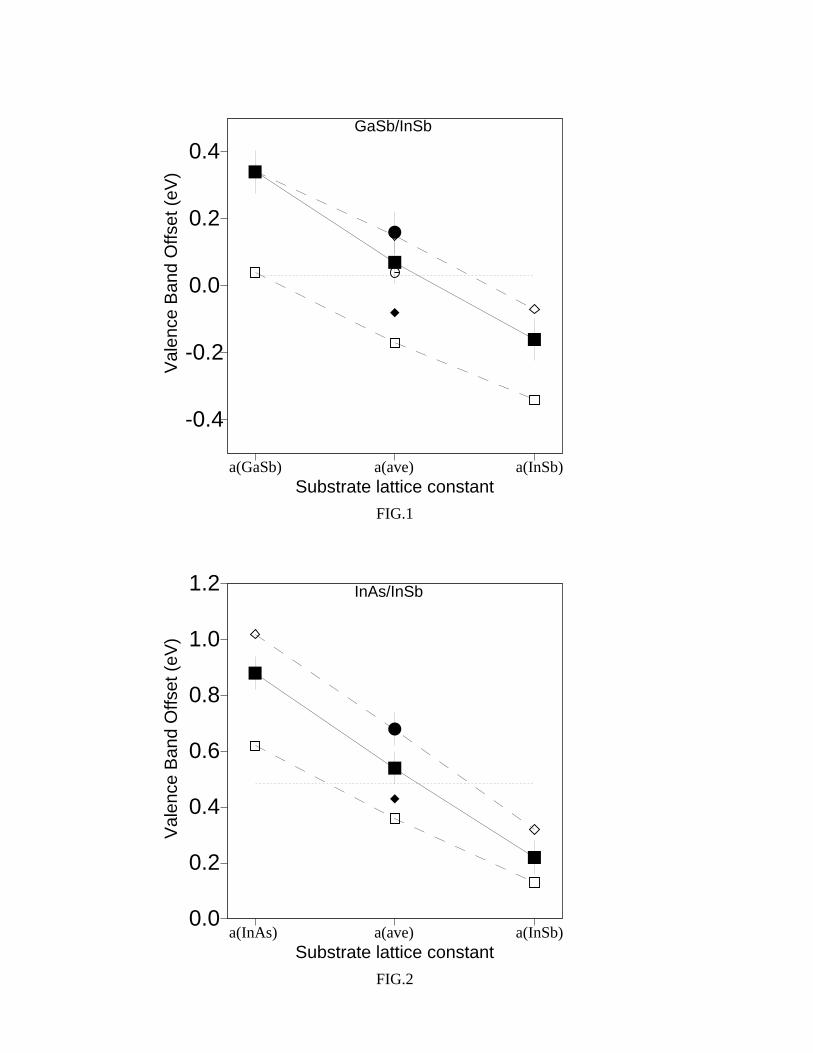
Figures 1 and 2, for common-anion and common-cation interfaces respectively, illustrate
7
the linear dependence (see the solid line in the figures) of the VBO on the lattice param-
eter which determines the SL pseudomorphic growth. Thus, the two figures show that the
GaSb/InSb and InAs/InSb SLs provide a good opportunity for tuning their VBO: a range
of about 0.5 eV for common-anion and of 0.7 eV for common-cation systems is covered by
varying the strain conditions determined by the substrate.
Let us now compare our results with other theoretical predictions, obtained from model
[6,23], semi-empirical [24] and ab-initio [10] calculations, as illustrated in Figures 1 and 2.
Note that all the predicted values agree with those of the present work (except those of
Ref. [23]), within their uncertainty of a few hundredths of an eV [6] and our error bars,
respectively. Incidentally, we observe that a similar disagreement between ab initio results
and those obtained by Cardona and Christensen [23] was also found in other III-V isovalent
heterojunctions, such as GaP/InP [10] and GaAs/InAs [11]. Furthermore, the linear trend of
the band offset as a function of the strain found in the present work is in excellent agreement
with the predictions of other theoretical work [6,23] and is reasonably expected to reproduce
the real situation.
So far, we have completely omitted a discussion of the conduction band offset (∆ Ec),
due to well known failures of LDA in predicting the correct band gap energies. However, we
should now point out that, using an approximate estimate of empirical band gaps (see Ref.
[17] for details), we can obtain information on the different kinds of band line-ups as growth
conditions are changed. In fact, we find a type I alignment for all the [001] common anion
interfaces, while [111] GaSb/InSb shows a type II staggered alignment (partial overlap of
the band gaps). On the other hand, for [001] common cation grown both on an InAs and
on an average substrate, we find a type II broken gap line-up, with the InAs conduction
band minimum lower in energy than the InSb VBM. Finally, the [001] InAs/InSb grown
on InSb and the [111] InAs/InSb heterojunctions contain a semimetallic compound (InAs),
thus leading to a type III alignment.
Starting from the results obtained from ab initio calculations [10,11,4,25] for different
[001] oriented strained layer interfaces (with similar lattice mismatch and grown on a sub-
8
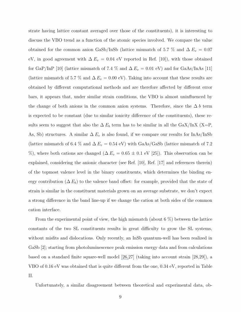
strate having lattice constant averaged over those of the constituents), it is interesting to
discuss the VBO trend as a function of the atomic species involved. We compare the value
obtained for the common anion GaSb/InSb (lattice mismatch of 5.7 % and ∆ Ev = 0.07
eV, in good agreement with ∆ Ev = 0.04 eV reported in Ref. [10]), with those obtained
for GaP/InP [10] (lattice mismatch of 7.4 % and ∆ Ev = 0.01 eV) and for GaAs/InAs [11]
(lattice mismatch of 5.7 % and ∆ Ev = 0.00 eV). Taking into account that these results are
obtained by different computational methods and are therefore affected by different error
bars, it appears that, under similar strain conditions, the VBO is almost uninfluenced by
the change of both anions in the common anion systems. Therefore, since the ∆ b term
is expected to be constant (due to similar ionicity difference of the constituents), these re-
sults seem to suggest that also the ∆ Eb term has to be similar in all the GaX/InX (X=P,
As, Sb) structures. A similar ∆ Ev is also found, if we compare our results for InAs/InSb
(lattice mismatch of 6.4 % and ∆ Ev = 0.54 eV) with GaAs/GaSb (lattice mismatch of 7.2
%), where both cations are changed (∆ Ev = 0.65 ± 0.1 eV [25]). This observation can be
explained, considering the anionic character (see Ref. [10], Ref. [17] and references therein)
of the topmost valence level in the binary constituents, which determines the binding en-
ergy contribution (∆ Eb) to the valence band offset: for example, provided that the state of
strain is similar in the constituent materials grown on an average substrate, we don’t expect
a strong difference in the band line-up if we change the cation at both sides of the common
cation interface.
From the experimental point of view, the high mismatch (about 6 %) between the lattice
constants of the two SL constituents results in great difficulty to grow the SL systems,
without misfits and dislocations. Only recently, an InSb quantum-well has been realized in
GaSb [2]; starting from photoluminescence peak emission energy data and from calculations
based on a standard finite square-well model [26,27] (taking into account strain [28,29]), a
VBO of 0.16 eV was obtained that is quite different from the one, 0.34 eV, reported in Table
II.
Unfortunately, a similar disagreement between theoretical and experimental data, ob-
9
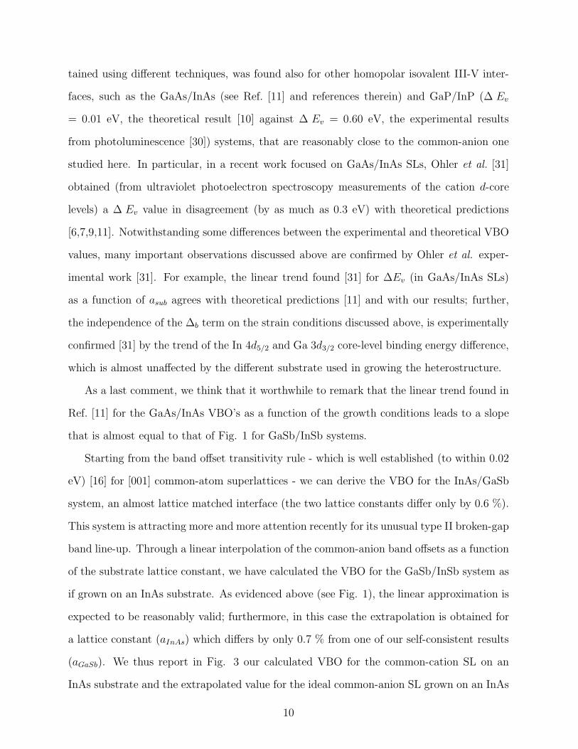
tained using different techniques, was found also for other homopolar isovalent III-V inter-
faces, such as the GaAs/InAs (see Ref. [11] and references therein) and GaP/InP (∆ Ev
= 0.01 eV, the theoretical result [10] against ∆ Ev = 0.60 eV, the experimental results
from photoluminescence [30]) systems, that are reasonably close to the common-anion one
studied here. In particular, in a recent work focused on GaAs/InAs SLs, Ohler et al. [31]
obtained (from ultraviolet photoelectron spectroscopy measurements of the cation d-core
levels) a ∆ Ev value in disagreement (by as much as 0.3 eV) with theoretical predictions
[6,7,9,11]. Notwithstanding some differences between the experimental and theoretical VBO
values, many important observations discussed above are confirmed by Ohler et al. exper-
imental work [31]. For example, the linear trend found [31] for ∆Ev (in GaAs/InAs SLs)
as a function of asub agrees with theoretical predictions [11] and with our results; further,
the independence of the ∆b term on the strain conditions discussed above, is experimentally
confirmed [31] by the trend of the In 4d5/2 and Ga 3d3/2 core-level binding energy difference,
which is almost unaffected by the different substrate used in growing the heterostructure.
As a last comment, we think that it worthwhile to remark that the linear trend found in
Ref. [11] for the GaAs/InAs VBO’s as a function of the growth conditions leads to a slope
that is almost equal to that of Fig. 1 for GaSb/InSb systems.
Starting from the band offset transitivity rule - which is well established (to within 0.02
eV) [16] for [001] common-atom superlattices - we can derive the VBO for the InAs/GaSb
system, an almost lattice matched interface (the two lattice constants differ only by 0.6 %).
This system is attracting more and more attention recently for its unusual type II broken-gap
band line-up. Through a linear interpolation of the common-anion band offsets as a function
of the substrate lattice constant, we have calculated the VBO for the GaSb/InSb system as
if grown on an InAs substrate. As evidenced above (see Fig. 1), the linear approximation is
expected to be reasonably valid; furthermore, in this case the extrapolation is obtained for
a lattice constant (aInAs) which differs by only 0.7 % from one of our self-consistent results
(aGaSb). We thus report in Fig. 3 our calculated VBO for the common-cation SL on an
InAs substrate and the extrapolated value for the ideal common-anion SL grown on an InAs
10
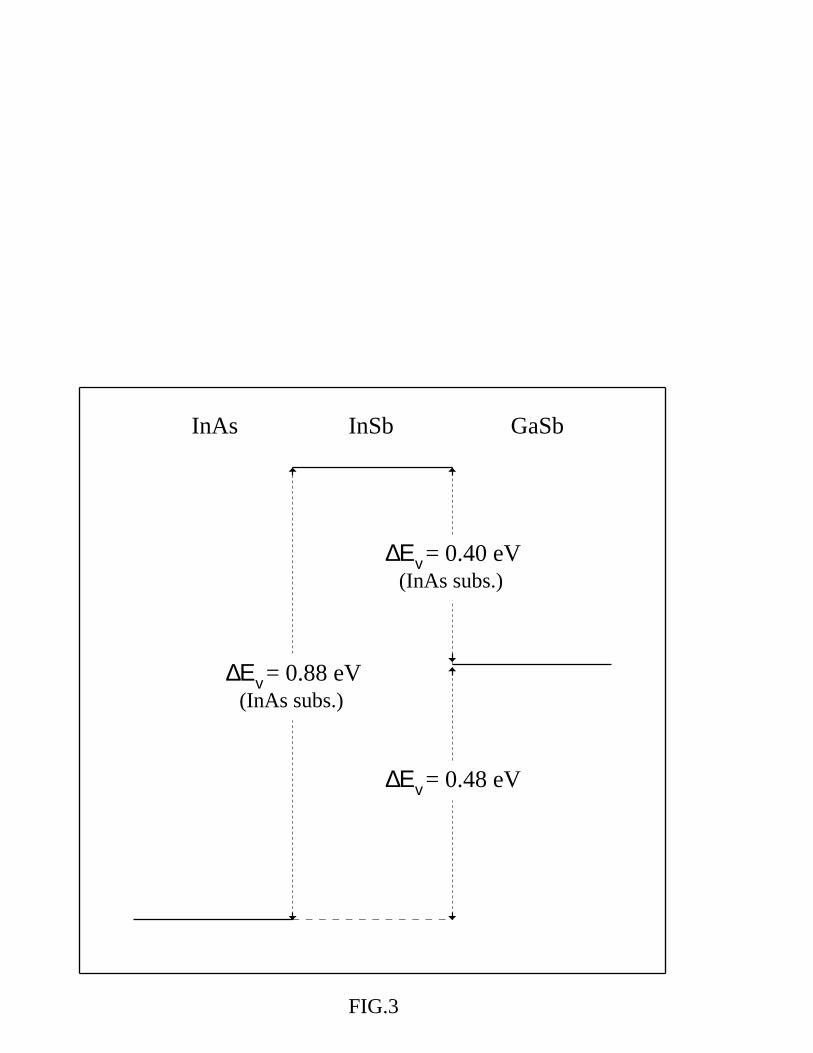
substrate. Using the transitivity rule, we obtain:
∆ Ev(InAs/GaSb) = ∆ Ev(InAs/InSb)InAs−subs. − ∆ Ev(InSb/GaSb)InAs−subs.
so that ∆Ev(InAs/GaSb)InAs−subs. = 0.88 - 0.40 = 0.48 eV. This result is in good agreement
with the available experimental values (0.46 eV [32], 0.51 eV [33]).
IV. CONCLUSIONS
In summary, we have studied the valence band offsets in [001] and [111] GaSb/InSb
and InAs/InSb interfaces by means of ab-initio FLAPW calculations, focusing our attention
on its dependence on ordering direction and strain conditions. Our results indicate that,
under the same strain conditions, the former has quite a small effect on the band line-up
mainly due to the different structural relaxation of the interface atoms at the [001] and [111]
heterojunctions. On the other hand, a much more important effect is due to pseudomorphic
growth on different substrates: the high tunability of the VBO (about 0.5 eV and 0.7 eV for
common-anion and for common-cation SLs, respectively) is evidenced by its linear decreasing
trend as the substrate lattice constant is increased, mainly due to the bulk contribution to
the band line-up. Finally, the transitivity rule was used to determine the InAs/GaSb valence
band offset and good agreement between theory and experiment was obtained.
V. ACKNOWLEDGEMENTS
We thank B. W. Wessels and M. Peressi for stimulating discussions and a careful read-
ing of the manuscript. Useful discussions with S. Massidda are also acknowledged. Work
at Northwestern University supported by the MRL Program of the National Science Foun-
dation, at the Materials Research Center of Northwestern University, under Award No.
DMR-9120521, and by a grant of computer time at the NSF supported Pittsburgh Super-
computing Center. Partial support by a supercomputing grant at Cineca (Bologna, Italy)
through the Consiglio Nazionale delle Ricerche (CNR) is also acknowledged.
11
TABLES
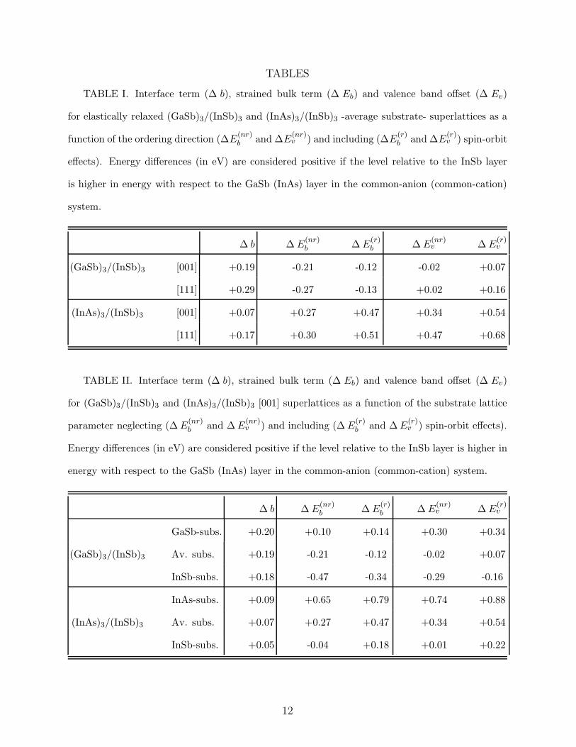
TABLE I. Interface term (∆ b), strained bulk term (∆ Eb) and valence band offset (∆ Ev)
for elastically relaxed (GaSb)3/(InSb)3 and (InAs)3/(InSb)3 -average substrate- superlattices as a
function of the ordering direction (∆E(nr)b and ∆E
(nr)v ) and including (∆E
(r)b and ∆E
(r)v ) spin-orbit
effects). Energy differences (in eV) are considered positive if the level relative to the InSb layer
is higher in energy with respect to the GaSb (InAs) layer in the common-anion (common-cation)
system.
∆ b ∆ E(nr)b ∆ E
(r)b ∆ E
(nr)v ∆ E
(r)v
(GaSb)3/(InSb)3 [001] +0.19 -0.21 -0.12 -0.02 +0.07
[111] +0.29 -0.27 -0.13 +0.02 +0.16
(InAs)3/(InSb)3 [001] +0.07 +0.27 +0.47 +0.34 +0.54
[111] +0.17 +0.30 +0.51 +0.47 +0.68
TABLE II. Interface term (∆ b), strained bulk term (∆ Eb) and valence band offset (∆ Ev)
for (GaSb)3/(InSb)3 and (InAs)3/(InSb)3 [001] superlattices as a function of the substrate lattice
parameter neglecting (∆ E(nr)b and ∆ E
(nr)v ) and including (∆ E
(r)b and ∆ E
(r)v ) spin-orbit effects).
Energy differences (in eV) are considered positive if the level relative to the InSb layer is higher in
energy with respect to the GaSb (InAs) layer in the common-anion (common-cation) system.
∆ b ∆ E(nr)b ∆ E
(r)b ∆ E
(nr)v ∆ E
(r)v
GaSb-subs. +0.20 +0.10 +0.14 +0.30 +0.34
(GaSb)3/(InSb)3 Av. subs. +0.19 -0.21 -0.12 -0.02 +0.07
InSb-subs. +0.18 -0.47 -0.34 -0.29 -0.16
InAs-subs. +0.09 +0.65 +0.79 +0.74 +0.88
(InAs)3/(InSb)3 Av. subs. +0.07 +0.27 +0.47 +0.34 +0.54
InSb-subs. +0.05 -0.04 +0.18 +0.01 +0.22
12
FIGURES
FIG. 1. Valence band offset (in eV) for GaSb-InSb SLs as a function of the substrate lattice
parameter. Our results (together with their error bars) are evidenced by filled squares ([001] SLs)
or filled circles ([111] SLs) and solid line. The dotted line shows the behaviour of unstrained GaSb
and InSb. Empty squares: Ref. [23]; empty diamonds: Ref. [6]; filled diamond: Ref. [24]; empty
circles: Ref. [10].
FIG. 2. Valence band offset (in eV) for InAs/InSb SLs as a function of the substrate lattice
parameter. Symbols are the same as those in Fig. 1.
FIG. 3. Valence band offset (in eV) for InAs/GaSb interface, obtained using the transitivity rule.
13
REFERENCES
[1] A.C.Gossard and S.Fafard, Sol. St. Comm. 72, 63 (1994).
[2] L.Q.Qian and B.W.Wessels, Appl. Phys. Lett. 63, 628 (1993).
[3] Robert G.Dandrea and Alex Zunger, Phys. Rev. B 43, 8962 (1991).
[4] A.Continenza, S.Massidda and A.J.Freeman, Phys. Rev. B 42, 3469 (1990).
[5] D. L. Smith and C. Mailhot, J. Appl. Phys. 62 (6), 25545 (1987).
[6] C.G.Van de Walle, Phys. Rev. B 39, 1871 (1989).
[7] C.Priester, G.Allan and M.Lannoo, Phys. Rev. B 38, 9870 (1988).
[8] M.Oloumi and C.C.Matthai, J. Phys. Condens. Matter 2, 5153 (1990)
[9] A.Taguchi and T.Ohno, Phys. Rev. B 39, 7803 (1989).
[10] A. Franceschetti, S.H.Wei and A.Zunger, Phys. Rev. B 50, 8094 (1994).
[11] N.Tit, M.Peressi and S.Baroni, Phys. Rev. B 48, 17607 (1993).
[12] H.J.F.Jansen and A.J.Freeman, Phys. Rev. B 30, 561 (1984); M.Weinert, H.Krakauer,
E.Wimmer and A.J.Freeman, Phys. Rev. B 24, 864 (1981).
[13] C. Mailhot and D. L. Smith, Phys. Rev. Lett. 58, 1264 (1987).
[14] D. L. Smith and C. Mailhot, Phys. Rev. B 35, 1242 (1987).
[15] R.G.Dandrea, C.B.Duke and A.Zunger, J. Vac. Sci. Technol. B10 (4), 1744 (1992).
[16] Y.Foulon and C.Priester, Phys. Rev. B 45, 6259 (1992).
[17] S.Picozzi, A.Continenza and A.J.Freeman, Phys. Rev. B 52, 5247 (1995).
[18] S. Massidda, B. I. Min and A. J. Freeman, Phys. Rev. B 35, 9871 (1987).
[19] R. Resta, S. Baroni and A. Baldereschi, Proc. 19th Int. Conf. on THE PHYSICS OF
14
SEMICONDUCTORS, edited by W. Zawadzki (Institute of Physics, Polish Academy of
Sciences, Wroclaw, 1988), p.255.
[20] S. Baroni, M. Peressi, R. Resta, A. Baldereschi, Theory of Band Offsets at Semiconduc-
tor Heterojunctions, in Proceedings of the 21th International Conference on the Physics
of Semiconductors, edited by Ping Jiang and Hou-Zhi Zheng (World Scientific, Singa-
pore, 1993), p. 689.
[21] C. G. Van de Walle and R. M. Martin, Phys. Rev. B 35, 8154 (1987).
[22] S. H. Wei and A. Zunger, Appl. Phys. Lett. 56, 662 (1990).
[23] M.Cardona and N.Christensen, Phys. Rev. B 35, 6182 (1987).
[24] A. Ichii, Y. Tsou and E. Garmine, J. Appl. Phys. 74 (3), 2112 (1993).
[25] S.H.Wei and A.Zunger, Phys. Rev. B 39, 3279 (1989).
[26] G.Bastard, Phys. Rev. B 24, 5693 (1981).
[27] K.Alavi et al., Electron. Lett. 19, 227 (1983).
[28] H.Asai and K.Oe, J. Appl. Phys. 54, 2052 (1983).
[29] G.Ji et al., J. Appl. Phys. 62, 3366 (1987).
[30] G. Armelles, M. C. Munoz and M. I. Alonso, Phys. Rev. B 47, 16299 (1993).
[31] C.Ohler et al., Phys. Rev. B 50, 7833 (1994).
[32] M. Jaros, Phys. Rev. B 37, 7112 (1988).
[33] H. Kroemer, J. Vac. Sci. Technol. B 2, 433 (1984).
15
a(GaSb) a(ave) a(InSb)
FIG.1
Substrate lattice constant
GaSb/InSb
-0.4
-0.2
0.0
0.2
0.4 V
alen
ce B
and
Offs
et (
eV)
a(InAs) a(ave) a(InSb)
FIG.2
Substrate lattice constant
InAs/InSb
0.0
0.2
0.4
0.6
0.8
1.0
1.2
Val
ence
Ban
d O
ffset
(eV
)
Ev∆ = 0.48 eV
Ev∆ = 0.40 eV(InAs subs.)
Ev∆ = 0.88 eV(InAs subs.)
InAs InSb GaSb
FIG.3