argon-ion-induced formation of nanoporous gasb layer: microstructure, infrared luminescence, and...
TRANSCRIPT

Argon-ion-induced formation of nanoporous GaSb layer: Microstructure, infraredluminescence, and vibrational propertiesD. P. Datta, A. Kanjilal, B. Satpati, S. Dhara, T. D. Das, D. Kanjilal, and T. Som
Citation: Journal of Applied Physics 116, 033514 (2014); doi: 10.1063/1.4890608 View online: http://dx.doi.org/10.1063/1.4890608 View Table of Contents: http://scitation.aip.org/content/aip/journal/jap/116/3?ver=pdfcov Published by the AIP Publishing Articles you may be interested in Nano-porosity in GaSb induced by swift heavy ion irradiation Appl. Phys. Lett. 104, 023105 (2014); 10.1063/1.4861747 Porosity-induced relaxation of strains in GaN layers studied by means of micro-indentation and opticalspectroscopy J. Appl. Phys. 111, 093513 (2012); 10.1063/1.4710994 Optical activation of Eu ions in nanoporous GaN films J. Appl. Phys. 99, 104305 (2006); 10.1063/1.2191647 Ion-irradiation-induced porosity in GaSb Appl. Phys. Lett. 86, 131920 (2005); 10.1063/1.1896428 Synthesis of GaN nanotip triangle pyramids on 3C–SiC epilayer/Si substrates via an in situ In-doping technique J. Chem. Phys. 122, 104713 (2005); 10.1063/1.1861880
[This article is copyrighted as indicated in the article. Reuse of AIP content is subject to the terms at: http://scitation.aip.org/termsconditions. Downloaded to ] IP:
14.139.193.129 On: Fri, 18 Jul 2014 14:39:44

Argon-ion-induced formation of nanoporous GaSb layer: Microstructure,infrared luminescence, and vibrational properties
D. P. Datta,1 A. Kanjilal,2 B. Satpati,3 S. Dhara,4 T. D. Das,5 D. Kanjilal,6 and T. Som1,a)
1SUNAG Laboratory, Institute of Physics, Bhubaneswar, Odisha 751 005, India2Department of Physics, Shiv Nadar University, Uttar Pradesh 201 314, India3Surface Physics and Material Science Division, Saha Institute of Nuclear Physics, 1/AF Bidhannagar,Kolkata 700 064, India4Surface and Nanoscience Division, Materials Science Group, Indira Gandhi Centre for Atomic Research,Kalpakkam 603 102, India5Department of Electronic Science, University of Calcutta, APC Road, Kolkata 700 009, India6Inter-University Accelerator Centre, Aruna Asaf Ali Marg, New Delhi 110 067, India
(Received 27 June 2014; accepted 8 July 2014; published online 18 July 2014)
Room temperature implantation of 60 keV Arþ-ions in GaSb to the fluences of 7� 1016 to 3� 1018
ions cm�2 is carried out at two incidence angles, viz 0� and 60�, leading to formation of a
nanoporous layer. As the ion fluence increases, patches grow on the porous layer under normal ion
implantation, whereas the porous layer gradually becomes embedded under a rough top surface for
oblique incidence of ions. Grazing incidence x-ray diffraction and cross-sectional transmission
electron microscopy studies reveal the existence of nanocrystallites embedded in the ion-beam
amorphized GaSb matrix up to the highest fluence used in our experiment. Oxidation of the nano-
porous layers becomes obvious from x-ray photoelectron spectroscopy and Raman mapping. The
correlation of ion-beam induced structural modification with photoluminescence signals in the
infrared region has further been studied, showing defect induced emission of additional peaks near
the band edge of GaSb. VC 2014 AIP Publishing LLC. [http://dx.doi.org/10.1063/1.4890608]
I. INTRODUCTION
GaSb nanostructures are considered to be promising for
low power electronic and optoelectronic devices operating in
near to mid-infrared wavelength range, owing to low band
gap and high carrier mobility of GaSb.1 For instance, GaSb
nanowires were utilized to fabricate single electron transistor
and infrared laser.2,3 In addition to several techniques used to
develop GaSb nanostructures,4,5 a porous layer containing
nanofibers has been developed in GaSb by ion-beam irradia-
tion with energy in the range of tens of keV to a few
MeV.6–13 Interestingly, the diameters of these nanofibers
are found to be in the range of 15–25 nm, irrespective of the
energy of the incident ions, whereas the thickness of the
nanoporous layer becomes an order of magnitude higher than
the range of ions with increasing fluence.6–13 The experimen-
tal investigations on porous structures formed in the low flu-
ence regime (<1016 ions cm�2) have shown residual
crystallinity in the nanofibers.8,10 It is, however, imperative to
explore whether nanocrystallites exist within the nanofibers
for fluences having orders of magnitude higher than those
reported earlier. This is predominantly significant in the con-
text of luminescence properties due to band-gap opening with
decreasing crystallite size.14 Crystalline GaSb is known to
exhibit photoluminescence (PL) in the infrared region
(700–800 meV) due to the radiative recombination of exci-
tons via band gap transitions.15–19 On the other hand, PL
emission in 785–805 meV was reported for GaSb nano-
wires.20 Moreover, visible range PL was reported for focused
ion-beam produced nanoporous structures (after post-
implantation annealing).11 Thus, the existence of nanocrystal-
lites in ion-induced porous layer can significantly influence
the PL emission from GaSb. Moreover, GaSb surface is prone
to oxidation owing to the reactive nature of Ga and Sb.21 In
fact, medium energy ion-beam induced formation of Ga2O3
and Sb2O3 at room temperature (RT) on the nanoporous
structures was confirmed in our previous report.12,13 The PL
emission from a nanoporous GaSb structure in presence of
these oxides is yet to be explored and understood, particularly
for structures generated by ion fluences orders of magnitude
higher from the previous studies.11
In this paper, we report the structural, compositional,
vibrational, and luminescence properties of the nanoporous
GaSb layers containing nanocrystallites, evolved under 60 keV
Arþ-ion implantation with fluences in the range of 7� 1016
� 3� 1018 ions cm�2. Subsequent to the demonstration of for-
mation of a porous structure by scanning electron microscopy
(SEM), the presence of nanocrystallites embedded in the
amorphous matrix will be shown by grazing incidence x-ray
diffraction (GIXRD) and transmission electron microscopy
(TEM) studies. Presence of Ga2O3 and Sb2O3 phases in the
porous layer will be demonstrated by x-ray photoelectron
spectroscopy (XPS) and Raman mapping. Using PL spectros-
copy, we will show infrared emission from such nanoporous
structures and attempt to correlate the emission with band gap
opening due to quantum confinement in the nanocrystallites.
II. EXPERIMENTAL
Mirror polished, p-type GaSb(100) substrates (area 1�1 cm2) were ultrasonically cleaned by using trichloroethylene,
a)Author to whom correspondence should be addressed. Electronic mail:
0021-8979/2014/116(3)/033514/7/$30.00 VC 2014 AIP Publishing LLC116, 033514-1
JOURNAL OF APPLIED PHYSICS 116, 033514 (2014)
[This article is copyrighted as indicated in the article. Reuse of AIP content is subject to the terms at: http://scitation.aip.org/termsconditions. Downloaded to ] IP:
14.139.193.129 On: Fri, 18 Jul 2014 14:39:44

acetone, ethanol, and de-ionized water and exposed to 60 keV
Arþ-ions at RT with fluences in the range of 7� 1016 to
3� 1018 ions cm�2. Two ion incidence angles (viz 0� and
60�) were chosen for the present experiments. Implantation-
induced evolution of microstructures was characterized by
using both SEM [Carl-Zeiss] and cross-sectional transmission
electron microscopy (XTEM) [field emission gun based
300 keV FEI Tecnai G2 S-Twin]. In addition, crystalline na-
ture of ion-irradiated samples was examined by employing
GIXRD (5�) measurements [D8-Discover, Bruker] using the
Cu-Ka radiation (k¼ 1.54 A) which was further corroborated
by selected area electron diffraction (SAED) during TEM
studies. Furthermore, surface chemical composition was
examined by XPS [VG Instruments] using Mg-Ka radiation
(h�¼ 1254 eV). Raman mapping was performed at RT by
using the 514 nm line of an Arþ-ion laser [inVia, Renishaw]
and the data were recorded with the help of a 1800 lines
nm�1 grating and a thermoelectrically cooled CCD detector.
The spectra were recorded in the backscattering geometry by
using a 100� objective with N.A. value of 0.85. The fully
automated motorized sample stage (Renishaw MS20), having
a spatial resolution of 100 nm, was used for Raman imaging.
This was performed by integrating intensities, which is essen-
tially the peak intensity distribution corresponding to a partic-
ular mode frequency collected over a pre-defined area and
grid resolution. In the present study, a total area of 2� 2 lm2
with 100� 600 nm2 grid resolution is probed for the Raman
mapping using the Stream Line imaging facility covering
large area. Low-temperature PL spectra were collected at
12 K using 532 nm line of a diode pumped solid state laser
with a surface power density of 1 W cm�2.
III. RESULTS AND DISCUSSION
The plan-view SEM images in Figs. 1(a) and 1(b) show
the surface morphology of Arþ-ion implanted samples at
h¼ 60�, whereas Figs. 1(c) and 1(d) illustrate the same cor-
responding to h¼ 0� which depict the evolution of porous
structures. As discerned from Figs. 1(a) and 1(c), corre-
sponding to the lowest fluence of 7� 1016 ions cm�2, the
porous layers comprise a network of nanofibers (diameter
15–25 nm). However, ridge-like structures are observed on
top of the porous network for h¼ 60�, whereas terrace-like
structures are developed on porous layer for h¼ 0�. The
fluence-dependent evolution of nanoporous structures for
h¼ 60� further demonstrates the impact of off-normal irradi-
ation. For instance, the porous layer gets embedded under a
continuous rough top surface at higher ion fluences (at 60�)[Fig. 1(b)], whereas large patches are observed on top of the
nanoporous layer under normal incidence [Fig. 1(d)]. It
should be mentioned that a modulated interface of the nano-
porous layer with the crystalline GaSb substrate underneath
was discernible in the cross-sectional SEM images for the
obliquely implanted samples.12
The presence of crystalline phases in the implantation-
induced nanoporous structure is evident from the GIXRD
data, where the spectra recorded from the samples implanted
at 60� and 0� are shown as a function of fluence in Figs. 2(a)
and 2(b), respectively. The collected spectra for both the
angles exhibit characteristic diffraction peaks at 2h¼ 25.4�,
FIG. 1. Plan-view SEM images of GaSb surfaces: Implanted with obliquely
incident (h¼ 60�) Arþ-ions to the fluences of 7� 1016 ions cm�2 (a) and
3� 1018 ions cm�2 (b) and normally incident Arþ-ions to the fluences of
7� 1016 ions cm�2 (c) and 3� 1018 ions cm�2 (d).
FIG. 2. GIXRD spectra of implanted GaSb samples: Arþ-ions incident at an
angle of 60� (a), and 0� (b), to the fluences of 7� 1016 ions cm�2 (red),
1� 1017 ions cm�2 (cyan), 4� 1017 ions cm�2 (blue), 7� 1017 ions cm�2 (ma-
genta), 1� 1018 ions cm�2 (dark yellow), and 3� 1018 ions cm�2 (green).
GIXRD data obtained from the pristine sample are also shown [black line in (a)]
for comparison. The spectra were shifted along the y-direction for better clarity.
033514-2 Datta et al. J. Appl. Phys. 116, 033514 (2014)
[This article is copyrighted as indicated in the article. Reuse of AIP content is subject to the terms at: http://scitation.aip.org/termsconditions. Downloaded to ] IP:
14.139.193.129 On: Fri, 18 Jul 2014 14:39:44
42�, and 50� which correspond to the (111), (200), and (311)
reflections from the cubic GaSb crystalline structure.22
Using the full width at half maximum (FWHM) of the (311)
diffraction peak in the Scherrer’s formula,23 the average
crystallite size has been estimated to be around 1.5–3.5 nm
for both the incident angles. Results obtained from GIXRD
are found to corroborate well with the findings of TEM anal-
yses described below.
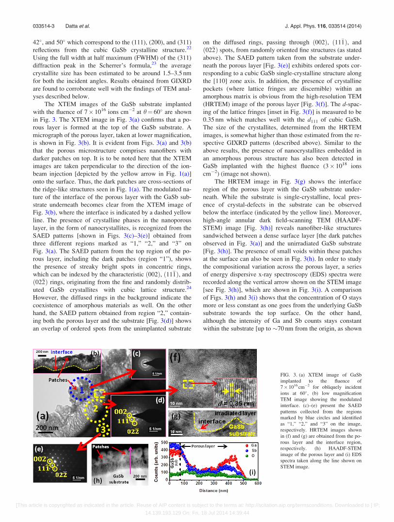
The XTEM images of the GaSb substrate implanted
with the fluence of 7� 1016 ions cm�2 at h¼ 60� are shown
in Fig. 3. The XTEM image in Fig. 3(a) confirms that a po-
rous layer is formed at the top of the GaSb substrate. A
micrograph of the porous layer, taken at lower magnification,
is shown in Fig. 3(b). It is evident from Figs. 3(a) and 3(b)
that the porous microstructure comprises nanofibers with
darker patches on top. It is to be noted here that the XTEM
images are taken perpendicular to the direction of the ion-
beam injection [depicted by the yellow arrow in Fig. 1(a)]
onto the surface. Thus, the dark patches are cross-sections of
the ridge-like structures seen in Fig. 1(a). The modulated na-
ture of the interface of the porous layer with the GaSb sub-
strate underneath becomes clear from the XTEM image of
Fig. 3(b), where the interface is indicated by a dashed yellow
line. The presence of crystalline phases in the nanoporous
layer, in the form of nanocrystallites, is recognized from the
SAED patterns [shown in Figs. 3(c)–3(e)] obtained from
three different regions marked as “1,” “2,” and “3” on
Fig. 3(a). The SAED pattern from the top region of the po-
rous layer, including the dark patches (region “1”), shows
the presence of streaky bright spots in concentric rings,
which can be indexed by the characteristic ð002Þ, ð11�1Þ, and
ð02�2Þ rings, originating from the fine and randomly distrib-
uted GaSb crystallites with cubic lattice structure.24
However, the diffused rings in the background indicate the
coexistence of amorphous materials as well. On the other
hand, the SAED pattern obtained from region “2,” contain-
ing both the porous layer and the substrate [Fig. 3(d)] shows
an overlap of ordered spots from the unimplanted substrate
on the diffused rings, passing through ð002Þ, ð11�1Þ, and
ð02�2Þ spots, from randomly oriented fine structures (as stated
above). The SAED pattern taken from the substrate under-
neath the porous layer [Fig. 3(e)] exhibits ordered spots cor-
responding to a cubic GaSb single-crystalline structure along
the [110] zone axis. In addition, the presence of crystalline
pockets (where lattice fringes are discernible) within an
amorphous matrix is obvious from the high-resolution TEM
(HRTEM) image of the porous layer [Fig. 3(f)]. The d-spac-
ing of the lattice fringes [inset in Fig. 3(f)] is measured to be
0.35 nm which matches well with the d111 of cubic GaSb.
The size of the crystallites, determined from the HRTEM
images, is somewhat higher than those estimated from the re-
spective GIXRD patterns (described above). Similar to the
above results, the presence of nanocrystallites embedded in
an amorphous porous structure has also been detected in
GaSb implanted with the highest fluence (3� 1018 ions
cm�2) (image not shown).
The HRTEM image in Fig. 3(g) shows the interface
region of the porous layer with the GaSb substrate under-
neath. While the substrate is single-crystalline, local pres-
ence of crystal-defects in the substrate can be observed
below the interface (indicated by the yellow line). Moreover,
high-angle annular dark field-scanning TEM (HAADF-
STEM) image [Fig. 3(h)] reveals nanofiber-like structures
sandwiched between a dense surface layer [the dark patches
observed in Fig. 3(a)] and the unirradiated GaSb substrate
[Fig. 3(h)]. The presence of small voids within these patches
at the surface can also be seen in Fig. 3(h). In order to study
the compositional variation across the porous layer, a series
of energy dispersive x-ray spectroscopy (EDS) spectra were
recorded along the vertical arrow shown on the STEM image
[see Fig. 3(h)], which are shown in Fig. 3(i). A comparison
of Figs. 3(h) and 3(i) shows that the concentration of O stays
more or less constant as one goes from the underlying GaSb
substrate towards the top surface. On the other hand,
although the intensity of Ga and Sb counts stays constant
within the substrate [up to �70 nm from the origin, as shown
FIG. 3. (a) XTEM image of GaSb
implanted to the fluence of
7� 1016 cm�2 for obliquely incident
ions at 60�, (b) low magnification
TEM image showing the modulated
interface. (c)–(e) present the SAED
patterns collected from the regions
marked by blue circles and identified
as “1,” “2,” and “3” on the image,
respectively. HRTEM images shown
in (f) and (g) are obtained from the po-
rous layer and the interface region,
respectively. (h) HAADF-STEM
image of the porous layer and (i) EDS
spectra taken along the line shown on
STEM image.
033514-3 Datta et al. J. Appl. Phys. 116, 033514 (2014)
[This article is copyrighted as indicated in the article. Reuse of AIP content is subject to the terms at: http://scitation.aip.org/termsconditions. Downloaded to ] IP:
14.139.193.129 On: Fri, 18 Jul 2014 14:39:44
by the dotted black line in Fig. 3(i)], subsequent decrease is
observed in the porous layer, followed by peaks at the top
surface of the porous layer [within the �400–500 nm region
in Fig. 3(i)]. The decrease in Ga and Sb counts seems to be
due to the porous nature of the layer, whereas the peaks near
the top surface are due to denser patches observed in the
XTEM and STEM images.
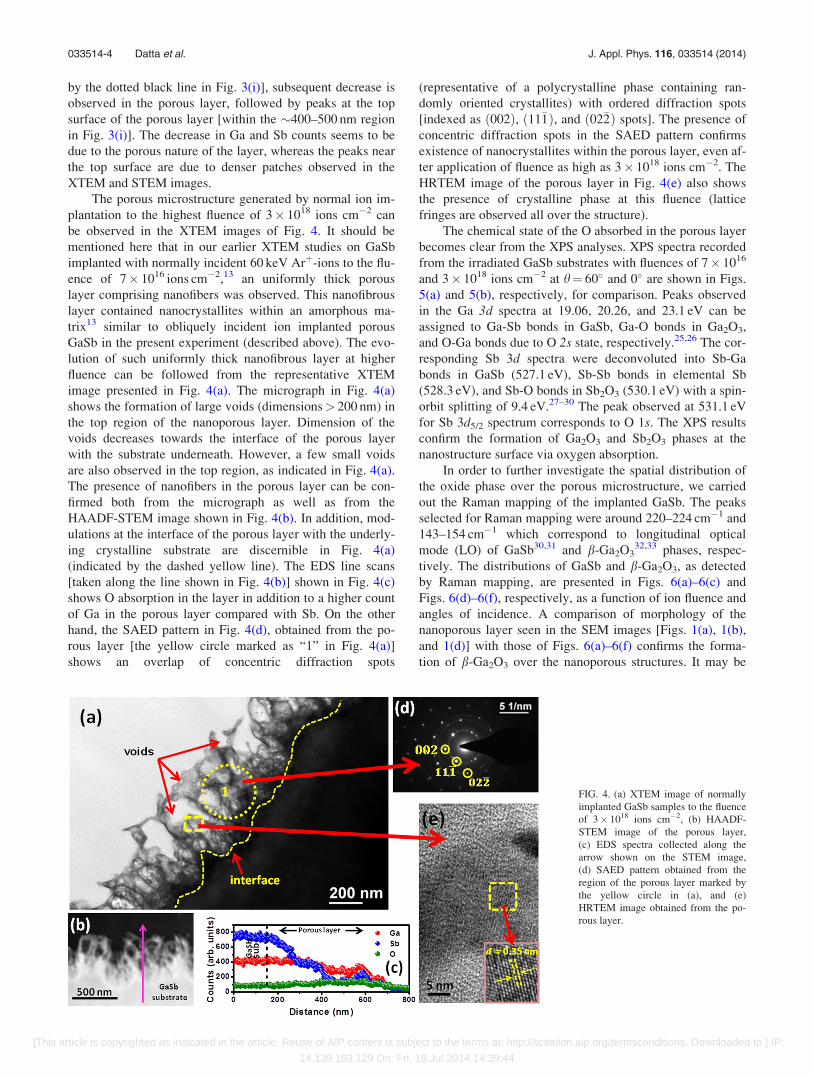
The porous microstructure generated by normal ion im-
plantation to the highest fluence of 3� 1018 ions cm�2 can
be observed in the XTEM images of Fig. 4. It should be
mentioned here that in our earlier XTEM studies on GaSb
implanted with normally incident 60 keV Arþ-ions to the flu-
ence of 7� 1016 ions cm�2,13 an uniformly thick porous
layer comprising nanofibers was observed. This nanofibrous
layer contained nanocrystallites within an amorphous ma-
trix13 similar to obliquely incident ion implanted porous
GaSb in the present experiment (described above). The evo-
lution of such uniformly thick nanofibrous layer at higher
fluence can be followed from the representative XTEM
image presented in Fig. 4(a). The micrograph in Fig. 4(a)
shows the formation of large voids (dimensions> 200 nm) in
the top region of the nanoporous layer. Dimension of the
voids decreases towards the interface of the porous layer
with the substrate underneath. However, a few small voids
are also observed in the top region, as indicated in Fig. 4(a).
The presence of nanofibers in the porous layer can be con-
firmed both from the micrograph as well as from the
HAADF-STEM image shown in Fig. 4(b). In addition, mod-
ulations at the interface of the porous layer with the underly-
ing crystalline substrate are discernible in Fig. 4(a)
(indicated by the dashed yellow line). The EDS line scans
[taken along the line shown in Fig. 4(b)] shown in Fig. 4(c)
shows O absorption in the layer in addition to a higher count
of Ga in the porous layer compared with Sb. On the other
hand, the SAED pattern in Fig. 4(d), obtained from the po-
rous layer [the yellow circle marked as “1” in Fig. 4(a)]
shows an overlap of concentric diffraction spots
(representative of a polycrystalline phase containing ran-
domly oriented crystallites) with ordered diffraction spots
[indexed as ð002Þ, ð11�1Þ, and ð02�2Þ spots]. The presence of
concentric diffraction spots in the SAED pattern confirms
existence of nanocrystallites within the porous layer, even af-
ter application of fluence as high as 3� 1018 ions cm�2. The
HRTEM image of the porous layer in Fig. 4(e) also shows
the presence of crystalline phase at this fluence (lattice
fringes are observed all over the structure).
The chemical state of the O absorbed in the porous layer
becomes clear from the XPS analyses. XPS spectra recorded
from the irradiated GaSb substrates with fluences of 7� 1016
and 3� 1018 ions cm�2 at h¼ 60� and 0� are shown in Figs.
5(a) and 5(b), respectively, for comparison. Peaks observed
in the Ga 3d spectra at 19.06, 20.26, and 23.1 eV can be
assigned to Ga-Sb bonds in GaSb, Ga-O bonds in Ga2O3,
and O-Ga bonds due to O 2s state, respectively.25,26 The cor-
responding Sb 3d spectra were deconvoluted into Sb-Ga
bonds in GaSb (527.1 eV), Sb-Sb bonds in elemental Sb
(528.3 eV), and Sb-O bonds in Sb2O3 (530.1 eV) with a spin-
orbit splitting of 9.4 eV.27–30 The peak observed at 531.1 eV
for Sb 3d5/2 spectrum corresponds to O 1s. The XPS results
confirm the formation of Ga2O3 and Sb2O3 phases at the
nanostructure surface via oxygen absorption.
In order to further investigate the spatial distribution of
the oxide phase over the porous microstructure, we carried
out the Raman mapping of the implanted GaSb. The peaks
selected for Raman mapping were around 220–224 cm�1 and
143–154 cm�1 which correspond to longitudinal optical
mode (LO) of GaSb30,31 and b-Ga2O332,33 phases, respec-
tively. The distributions of GaSb and b-Ga2O3, as detected
by Raman mapping, are presented in Figs. 6(a)–6(c) and
Figs. 6(d)–6(f), respectively, as a function of ion fluence and
angles of incidence. A comparison of morphology of the
nanoporous layer seen in the SEM images [Figs. 1(a), 1(b),
and 1(d)] with those of Figs. 6(a)–6(f) confirms the forma-
tion of b-Ga2O3 over the nanoporous structures. It may be
FIG. 4. (a) XTEM image of normally
implanted GaSb samples to the fluence
of 3� 1018 ions cm�2, (b) HAADF-
STEM image of the porous layer,
(c) EDS spectra collected along the
arrow shown on the STEM image,
(d) SAED pattern obtained from the
region of the porous layer marked by
the yellow circle in (a), and (e)
HRTEM image obtained from the po-
rous layer.
033514-4 Datta et al. J. Appl. Phys. 116, 033514 (2014)
[This article is copyrighted as indicated in the article. Reuse of AIP content is subject to the terms at: http://scitation.aip.org/termsconditions. Downloaded to ] IP:
14.139.193.129 On: Fri, 18 Jul 2014 14:39:44
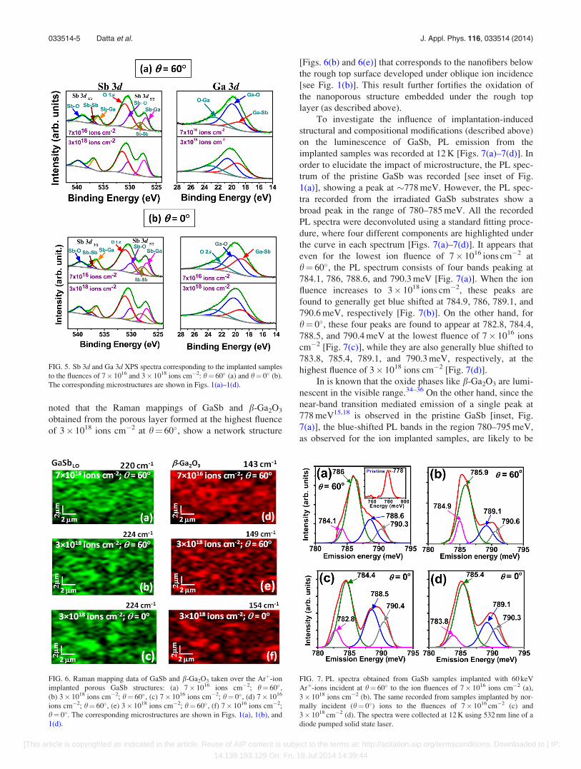
noted that the Raman mappings of GaSb and b-Ga2O3
obtained from the porous layer formed at the highest fluence
of 3� 1018 ions cm�2 at h¼ 60�, show a network structure
[Figs. 6(b) and 6(e)] that corresponds to the nanofibers below
the rough top surface developed under oblique ion incidence
[see Fig. 1(b)]. This result further fortifies the oxidation of
the nanoporous structure embedded under the rough top
layer (as described above).
To investigate the influence of implantation-induced
structural and compositional modifications (described above)
on the luminescence of GaSb, PL emission from the
implanted samples was recorded at 12 K [Figs. 7(a)–7(d)]. In
order to elucidate the impact of microstructure, the PL spec-
trum of the pristine GaSb was recorded [see inset of Fig.
1(a)], showing a peak at �778 meV. However, the PL spec-
tra recorded from the irradiated GaSb substrates show a
broad peak in the range of 780–785 meV. All the recorded
PL spectra were deconvoluted using a standard fitting proce-
dure, where four different components are highlighted under
the curve in each spectrum [Figs. 7(a)–7(d)]. It appears that
even for the lowest ion fluence of 7� 1016 ions cm�2 at
h¼ 60�, the PL spectrum consists of four bands peaking at
784.1, 786, 788.6, and 790.3 meV [Fig. 7(a)]. When the ion
fluence increases to 3� 1018 ions cm�2, these peaks are
found to generally get blue shifted at 784.9, 786, 789.1, and
790.6 meV, respectively [Fig. 7(b)]. On the other hand, for
h¼ 0�, these four peaks are found to appear at 782.8, 784.4,
788.5, and 790.4 meV at the lowest fluence of 7� 1016 ions
cm�2 [Fig. 7(c)], while they are also generally blue shifted to
783.8, 785.4, 789.1, and 790.3 meV, respectively, at the
highest fluence of 3� 1018 ions cm�2 [Fig. 7(d)].
In is known that the oxide phases like b-Ga2O3 are lumi-
nescent in the visible range.34–36 On the other hand, since the
near-band transition mediated emission of a single peak at
778 meV15,18 is observed in the pristine GaSb [inset, Fig.
7(a)], the blue-shifted PL bands in the region 780–795 meV,
as observed for the ion implanted samples, are likely to be
FIG. 5. Sb 3d and Ga 3d XPS spectra corresponding to the implanted samples
to the fluences of 7� 1016 and 3� 1018 ions cm�2: h¼ 60� (a) and h¼ 0� (b).
The corresponding microstructures are shown in Figs. 1(a)–1(d).
FIG. 6. Raman mapping data of GaSb and b-Ga2O3 taken over the Arþ-ion
implanted porous GaSb structures: (a) 7� 1016 ions cm�2; h¼ 60�,(b) 3� 1018 ions cm�2; h¼ 60�, (c) 7� 1016 ions cm�2; h¼ 0�, (d) 7� 1016
ions cm�2; h¼ 60�, (e) 3� 1018 ions cm�2; h¼ 60�, (f) 7� 1016 ions cm�2;
h¼ 0�. The corresponding microstructures are shown in Figs. 1(a), 1(b), and
1(d).
FIG. 7. PL spectra obtained from GaSb samples implanted with 60 keV
Arþ-ions incident at h¼ 60� to the ion fluences of 7� 1016 ions cm�2 (a),
3� 1018 ions cm�2 (b). The same recorded from samples implanted by nor-
mally incident (h¼ 0�) ions to the fluences of 7� 1016 cm�2 (c) and
3� 1018 cm�2 (d). The spectra were collected at 12 K using 532 nm line of a
diode pumped solid state laser.
033514-5 Datta et al. J. Appl. Phys. 116, 033514 (2014)
[This article is copyrighted as indicated in the article. Reuse of AIP content is subject to the terms at: http://scitation.aip.org/termsconditions. Downloaded to ] IP:
14.139.193.129 On: Fri, 18 Jul 2014 14:39:44
associated with the GaSb nanocrystallites15–20 embedded in
an amorphous matrix. Earlier observations of PL emission
from GaSb, in the range of 770–800 meV, were discussed in
terms of donor-acceptor pair transitions and bound excitonic
transitions.15–20 In fact, the PL line observed around
779 meV is usually assigned to a donor-acceptor pair transi-
tion (denoted as A band), involving the neutral state of the
native acceptor.15,18 Although Iyer et al. showed that the
peak can shift to 780 meV for highly doped GaSb,17 this can-
not be the case in the present scenario since the GaSb wafers
are undoped. Meanwhile, the peak observed at around
784.4 meV was also observed by Iyer et al. but the origin of
this peak was unidentified.16 Bosacchi et al. also reported a
PL peak at 788 meV from crystalline bulk GaSb which was
correlated to a donor to carbon pair recombination.18 On the
other hand, Ploog et al. recorded a PL peak at 784 meV from
a quantum well structure of GaSb and correlated it to
electron-heavy hole transition.19 In addition, Jeppsson et al.demonstrated a dominant PL peak between 785 and
800 meV for GaSb nanowire structures,20 although the origin
of the radiative transition could not be identified. A compari-
son between PL spectra obtained in the present case with
those reported earlier, especially, with PL emission from
nanoscale structures,19,20 indicates that the observed blue
shift in the PL emission can be attributed to three-
dimensional quantum confinement in GaSb nanocrystallites
due to the opening of the effective band gap by decreasing
the average crystallite size37 with increasing ion fluence.
This is further confirmed by the XTEM studies (only a few
nanometers) showing the formation of nanocrystallites with
sizes smaller than the Bohr radius of GaSb, namely,
20.48 nm.11 However, the insignificant difference in PL peak
positions in Figs. 7(a) and 7(b), namely, 786 and 785.9 meV
(corresponding to fluences of 7� 1016 and 3� 1018 ions
cm�2 at h¼ 60�, respectively) is not clear yet, but looking at
blue shifts in other PL peak positions, it seems that the peak
residing at 786 meV is originating from radiative defect cen-
ters. The blue shift from 784.4 to 785.4 meV, observed in
Figs. 7(c) and 7(d), corresponding to h¼ 0�, can be associ-
ated with a decrease in average crystallite size with increas-
ing ion fluence. We should note here that such a systematic
shift in PL peak position, especially for emission peaks
below and above 785 meV [Figs. 7(a)–7(d)] as a function of
fluence cannot be explained in light of defect-related radia-
tive recombination of excitons as predicted earlier by several
authors.14–19
We now give an account of the origin of GaSb nanocrys-
tallites that remain embedded in the porous microstructure in
order to understand the observed blue shift in PL emission.
The processes that lead to the formation of a nanoporous
layer containing nanofibers were discussed in detail in Ref.
12. In short, during the early stage of implantation, the
vacancies created in GaSb due to ion energy loss agglomer-
ate into voids. The voids grow in size with irradiation as the
vacancies created by further ion irradiation migrate to the
existing voids. Finally, the interconnections of the growing
voids result in a porous structure. At the same time, redepos-
ited sputtered atoms on top of the porous layer lead to the
formation of patches or ridge-like structures. A continuous
top surface is formed at higher fluences in case of off-
normally incident ions because of much higher rate of re-
deposition. This mechanism of formation of nanoporous
layer is associated with the presence of crystallites observed
in the present experiment. When the nanoporous layer is
formed, the incident ions dissipate very small amount of
energy in the layer (only during their passage through the
nano-dimensional GaSb remaining in the porous layer).12
Since the porous layer in GaSb starts to form at ion fluence
as low as� 1014–1015 ions cm�2,6–10 it can be expected that
ion-beam induced amorphization of GaSb remains incom-
plete and leaves behind the nanocrystallites embedded in the
amorphous nanofibrous structure. During subsequent stages
of implantation, very small amount of the incident energy is
deposited in the nanoporous layer, which is insufficient for
complete amorphization of the embedded crystallites.12
IV. CONCLUSIONS
In summary, we report on detail morphological and micro-
structural studies along with vibrational properties and infrared
luminescence of medium energy Arþ-ion implantation induced
porous GaSb in the high fluence regime (7� 1016 – 3� 1018
ions cm�2). Our studies demonstrate the presence of crystalline
phases in the amorphous matrix of the nanoporous layer till the
highest fluence of 3� 1018 ions cm�2. The nanoporous layer
turns out to be oxidized with the existence of b-Ga2O3 on the
surface of the nanostructures, and is also found to be lumines-
cent in the infrared regime, presumably because of quantum
confinement of excitons in GaSb nanocrystallites. Moreover,
the observed blue shift of the deconvoluted PL bands is dis-
cussed in light of gap opening with decreasing GaSb nanocrys-
tallite size as a function of ion fluence.
ACKNOWLEDGMENTS
Authors gratefully acknowledge helps received from
Professor S. Varma, from Institute of Physics, Bhbaneswar for
XPS studies, Professor S. Dhar, Department of Electronic
Science, University of Calcutta, Kolkata for PL measurements,
and Professor P. K. Sahoo, National Institute of Science
Education and Research, Bhubaneswar, for extending SEM
facility. Mr. S. K. Garg, SUNAG Lab, Institute of Physics is
acknowledged for his help during implantations. Helps
received from T. Basu and M. Kumar, SUNAG Lab, Institute
of Physics during the experiments are also acknowledged.
1P. S. Dutta, H. L. Bhat, and V. Kumar, J. Appl. Phys. 81, 5821 (1997).2A. H. Chin, S. Vaddiraju, A. V. Maslov, C. Z. Ning, M. K. Sunkara, and
M. Meyyappan, Appl. Phys. Lett. 88, 163115 (2006).3B. M. Borg, K. A. Dick, B. Ganjipour, M. E. Pistol, L. E. Wernersson, and
C. Thelander, Nano Lett. 10, 4080 (2010).4Y. N. Guo, J. Zou, M. Paladugu, H. Wang, Q. Gao, H. H. Tan, and C.
Jagadish, Appl. Phys. Lett. 89, 231917 (2006).5S. Schulz, M. Schwartz, A. Kuczkowski, and W. Assenmacher, J. Cryst.
Growth 312, 1475 (2010).6N. Nitta, M. Taniwaki, Y. Hayashi, and T. Yoshiie, J. Appl. Phys. 92,
1799 (2002).7N. Nitta and M. Taniwaki, Phys. B: Condens. Matter 376–377, 872 (2006).8S. M. Kluth, J. D. Fitz Gerald, and M. C. Ridgway, Appl. Phys. Lett. 86,
131920 (2005).9P. Kluth, S. M. Kluth, B. Johannessen, C. J. Glover, G. J. Foran, and M. C.
Ridgway, J. Appl. Phys. 110, 113528 (2011).
033514-6 Datta et al. J. Appl. Phys. 116, 033514 (2014)
[This article is copyrighted as indicated in the article. Reuse of AIP content is subject to the terms at: http://scitation.aip.org/termsconditions. Downloaded to ] IP:
14.139.193.129 On: Fri, 18 Jul 2014 14:39:44
10A. Perez-Bergquist, S. Zhu, K. Sun, X. Xiang, Y. Zhang, and L. Wang,
Small 4, 1119 (2008).11X. Zhou, W. Guo, A. G. Perez-Bergquist, Q. Wei, Y. Chen, K Sun, and L.
Wang, Nanoscale Res. Lett. 6, 6 (2011).12D. P. Datta, A. Kanjilal, S. K. Garg, P. K. Sahoo, D. Kanjilal, and T. Som,
J. Appl. Phys. 115, 123515 (2014).13D. P. Datta, A. Kanjilal, S. K. Garg, P. K. Sahoo, B. Satpati, D. Kanjilal,
and T. Som, Appl. Surf. Sci. 310, 189 (2014).14A. M. Smith and S. Nie, Acc. Chem. Res. 43, 190 (2010).15L. Tirado-Mej�ıa, J. A. Villada, M. delosR�ıos, J. A. Pe~nafiel, G. Fonthal, D.
G. Espinosa-Arbel�aez, H. Ariza-Calder�on, and M. E. Rodr�ıguez-Garc�ıa,
Physica B 403, 4027 (2008).16S. Iyer, S. Hegde, K. K. Bajaj, A. Abul-Fadl, and W. Mitchel, J. Appl.
Phys. 73, 3958 (1993).17S. Iyer, L. Small, S. Hegde, K. K. Bajaj, and A. Abul-Fadl, J. Appl. Phys.
77, 5902 (1995).18A. Bosacchi et al., J. Cryst. Growth 150, 844 (1995).19K. Ploog, Y. Ohmori, H. Okamoto, W. Stolz, and J. Wagner, Appl. Phys.
Lett. 47, 384 (1985).20M. Jeppsson et al., J. Cryst. Growth 310, 5119 (2008).21R. Callec, P. N. Favennec, M. Salvi, H. L’Haridon, and M. Gauneau,
Appl. Phys. Lett. 59, 1872 (1991).22X-Ray diffraction database JCPDS-International Centre for Diffraction
Data, 07-0215 (1998).
23A. Kanjilal, Nanotechnology 13, 682 (2002).24D. B. Williams and C. Barry Carter, Transmission Electron Microscopy
(Springer, New York, 2009).25I. Geppert, M. Eizenberg, A. Ali, and S. Datta, Appl. Phys. Lett. 97,
162109 (2010).26V. M. Bermudez, J. Appl. Phys. 114, 024903 (2013).27Y. Sun and M. Wu, J. Appl. Phys. 78, 6691 (1995).28H. K. Kim, J. H. Jung, and D. J. Choi, Thin Solid Films 520, 6947
(2012).29D. M. Zhernokletov, H. Dong, B. Brennan, M. Yakimov, V. Tokranov, S.
Oktyabrsky, J. Kim, and R. M. Wallace, Appl. Phys. Lett. 102, 131602
(2013).30D. M. Murape, N. Eassa, J. H. Neethling, R. Betz, E. Coetsee, H. C. Swart,
J. R. Botha, and A. Venter, Appl. Surf. Sci. 258, 6753 (2012).31S. G. Kim, H. Asahi, M. Seta, J. Takijawa, S. Emura, R. K. Soni, and S.
Gonda, J. Appl. Phys. 74, 579 (1993).32J. H. Dias da Silva, S. W. da Silva, and J. W. Galzerani, J. Appl. Phys. 77,
4044 (1995).33Y. H. Gao, Y. Bando, T. Sato, Y. F. Zhang, and X. Q. Gao, Appl. Phys.
Lett. 81, 2267 (2002).34P. Guha, S. Chakrabarty, and S. Chaudury, Physica B 23, 81 (2004).35R. Jangir et al., J. Appl. Phys. 112, 034307 (2012).36A. Khan, W. Jadwisienczak, and M. Kordesch, Physica E 35, 207 (2006).37B. D. Diwan and V. B. Dubey, AIP Conf. Proc. 1536, 279 (2013).
033514-7 Datta et al. J. Appl. Phys. 116, 033514 (2014)
[This article is copyrighted as indicated in the article. Reuse of AIP content is subject to the terms at: http://scitation.aip.org/termsconditions. Downloaded to ] IP:
14.139.193.129 On: Fri, 18 Jul 2014 14:39:44