atlas liquid argon calorimeter front end electronics
TRANSCRIPT

This content has been downloaded from IOPscience. Please scroll down to see the full text.
Download details:
IP Address: 221.130.23.148
This content was downloaded on 20/10/2013 at 11:57
Please note that terms and conditions apply.
ATLAS liquid argon calorimeter front end electronics
View the table of contents for this issue, or go to the journal homepage for more
2008 JINST 3 P09003
(http://iopscience.iop.org/1748-0221/3/09/P09003)
Home Search Collections Journals About Contact us My IOPscience

2008 JINST 3 P09003
PUBLISHED BY INSTITUTE OFPHYSICS PUBLISHING AND SISSA
RECEIVED: April 21, 2008REVISED: July 30, 2008
ACCEPTED: September 1, 2008PUBLISHED: September 19, 2008
ATLAS liquid argon calorimeter front end electronics
N.J. Buchanan, a,1 L. Chen, a,2 D.M. Gingrich, a,3 S. Liu, a H. Chen,b D. Damazio, b
F. Densing, b S. Duffin, b J. Farrell, b S. Kandasamy, b J. Kierstead, b F. Lanni, b
D. Lissauer, b H. Ma,b D. Makowiecki, b T. Muller, b V. Radeka,b S. Rescia, b
R. Ruggiero, b H. Takai,b K. Wolniewicz, b H. Ghazlane, c A. Hoummada, c L. Hervas, d
T. Hott, d,4 H.G. Wilkens, d J. Ban, e,5 S. Boettcher, e,6 G. Brooijmans, e C.-Y. Chi,e
S. Caughron, e M. Cooke, e K. Copic, e D. Dannheim, e,7 A. Gara,e,8 A. Haas,e
I. Katsanos, e J.A. Parsons, e∗S. Simion, e,9 W. Sippach, e L. Zhang, e N. Zhou, e
P. Eckstein, f M. Kobel, f E. Ladygin, g E. Auge, h R. Bernier, h M. Bouchel, h
A. Bozzone, h D. Breton, h C. de la Taille, h I. Falleau, h D. Fournier, h P. Imbert, h
G. Martin-Chassard, h A. Perus, h J.P. Richer, h,10 N. Seguin Moreau, h L. Serin, h
V. Tocut, h J-J. Veillet, h D. Zerwas, h J. Colas, i N. Dumont-Dayot, i N. Massol, i
P. Perrodo, i G. Perrot, i I. Wingerter-Seez, i M. Escalier, j F. Hubaut, j,11 B. Laforge, j
O. Le Dortz, j Ph. Schwemling, j J. Collot, k D. Dzahini, k M.-L. Gallin-Martel, k
P. Martin, k W.D. Cwienk, l J. Fent, l L. Kurchaninov, l ,12 M. Citterio, m M. Mazzanti, m
F. Tartarelli, m V. Bansal, n C. Boulahouache, n W. Cleland, n B. Liu, n J. McDonald, n
V. Paolone, n J. Rabel, n V. Savinov, n G. Zuk,n K. Benslama, o P. Borgeaud, p
X. de la Broïse, p E. Delagnes, p A. Le Coguie, p B. Mansoulié, p J. Pascual, p
J. Teiger, p B. Dinkespiler, q,13 T. Liu, q R. Stroynowski, q J. Ye,q P. Zarzhitsky, q
K.-J. Grahn, r P. Hansson, r B. Lund-Jensen, r M.L. Chu, s S.-C. Lee,s D.S. Su,s
P.K. Teng s and H.M. Braun t
aCentre for Particle Physics, Department of Physics, University of Alberta,Edmonton, Alberta, Canada
bBrookhaven National Laboratory (BNL), Upton, NY, U.S.A.cFaculté des Sciences,University of Casablanca, Casablanca, MoroccodCERN, Geneva, SwitzerlandeColumbia University, Nevis Laboratories, Irvington, NY, U.S.A.f Technische Universität Dresden, Dresden, GermanygJoint Institute for Nuclear Research, Dubna, RussiahLaboratoire de l’Accélérateur Linéaire (LAL), Orsay, FranceiLaboratoire d’Annecy-le-Vieux de Physique des Particules(LAPP),Université de Savoie, Annecy, France
jLPNHE, Université Pierre et Marie Curie Paris 6, UniversitéDenis Diderot Paris 7,CNRS/IN2P3, Paris, France
– 1 –

2008 JINST 3 P09003
kLPSC, Université Joseph Fourier Grenoble 1, CNRS/IN2P3,Institut National Polytechnique de Grenoble, Grenoble, France
l Max-Planck-Institut für Physik, Werner-Heisenberg-Institut, Munich, GermanymDipartimento di Fisica dell’Università di Milano and INFN,Milano, ItalynUniversity of Pittsburgh, Pittsburgh, Pennsylvania, U.S.A.oUniversity of Regina, Regina, Saskatchewan, CanadapDSM/Irfu, CEA-Saclay, F-91191 Gif-sur-Yvette Cedex, FranceqSouthern Methodist University, Dallas, Texas, U.S.A.rRoyal Institute of Technology (KTH), Stockholm, SwedensInstitute of Physics, Academia Sinica, Nankang, Taipei, Taiwan, R.O.C.tUniversity of Wuppertal, Wuppertal, Germany1Now at Department of Physics, Colorado State University, Fort Collins, Colorado, U.S.A.2Now at Department of Electrical and Computer Engineering, University of Saskatchewan,Saskatoon, Saskatchewan, Canada
3Also at TRIUMF, Vancouver, British Columbia, Canada4Now at DESY, Hamburg, Germany5Also at Institute of Experimental Physics, Kosice, Slovakia6Now at Christian Albrechts University, Institute for Experimental and Applied Physics, Kiel,Germany
7Now at CERN8Now at IBM T.J. Watson Research Center, U.S.A.9Now at LAL
10Now at LPSC11Now at CPPM12Now at TRIUMF13Now at CPPM
E-mail: [email protected]
ABSTRACT: The ATLAS detector has been designed for operation at CERN’s Large Hadron Col-lider. ATLAS includes a complex system of liquid argon calorimeters. This paper describes thearchitecture and implementation of the system of custom front end electronics developed for thereadout of the ATLAS liquid argon calorimeters.
KEYWORDS: Electronic detector readout concepts (gas, liquid); Calorimeters; Front-endelectronics for detector readout.
∗Corresponding author.
c© 2008 IOP Publishing Ltd and SISSA http://www.iop.org/EJ/jinst/

2008 JINST 3 P09003
Contents
1. Introduction 2
2. Overview of ATLAS LAr Front End electronics 2
3. Front End electronics boards 63.1 Front End board 63.2 Calibration board 83.3 Controller board 9
4. Level 1 trigger electronics 154.1 Tower Builder Board 154.2 Tower Driver Board 194.3 Receiver/monitor system 21
5. Front End Crate infrastructure and services 275.1 Pedestal and feedthrough services 285.2 Front End Crate mechanical assembly 295.3 Power bus 305.4 SPAC bus 305.5 Baseplane 325.6 Optical cables 355.7 Cooling distribution 365.8 Monitoring system 37
6. Low voltage power supplies and distribution 386.1 280 V power supplies 386.2 Low voltage power supplies 386.3 HEC low voltage system 41
7. High voltage power supplies and distribution 42
8. Grounding scheme 45
9. Cable plant 47
10. Summary 47
A. The SPAC serial control system 48
B. Implementation of the Front End Crate Monitoring System 50
C. Photographs of components of the Front End Crate infrastructure 53
– 1 –

2008 JINST 3 P09003
D. Acronyms used in the paper 55
1. Introduction
ATLAS [1] is a large general-purpose detector designed for operation at the Large Hadron Collider(LHC) at CERN. The LHC is a proton-proton collider which willoperate with a center-of-massenergy of 14 TeV. A system of liquid argon (LAr) calorimetersforms one of the major ATLASdetector systems. The LAr calorimeter system is composed ofan electromagnetic (EM) calorimetercovering the region of pseudorapidity|η | < 3.2, a hadronic endcap (HEC) calorimeter covering1.5< |η | < 3.2, and a forward calorimeter (FCAL) covering 3.1< |η | < 4.9. These elements arehoused in three cryostats. The central (barrel) cryostat contains the barrel EM calorimeter (EMB),which covers|η | < 1.5. There are two endcap (EC) cryostats, each containing one side of theendcap EM calorimeter (EMEC), the HEC and the FCAL. Each element of the LAr calorimetersystem is segmented in depth: the EMB and EMEC each have four layers (presampler, strips,middle and back), the HEC has three layers, and the FCAL also has three (one electromagneticlayer and two hadronic layers). More details about the design, construction, and performance ofthe calorimeters themselves can be found in reference [2].
As depicted schematically in figure 1, the electronic readout of the ATLAS LAr calorimetersis divided into a Front End (FE) system of boards mounted in custom crates directly on the cryo-stat feedthroughs, and a Back End (BE) system of VME-based boards located in an off-detectorunderground counting house (dubbed USA15) where there is noradiation. The design and imple-mentation of the BE system, which includes Digital Signal Processor (DSP) electronics for digitalfiltering of the readout signals in order to reconstruct the deposited energy and other quantities, aredescribed in reference [3]. The purpose of this note is to describe the overall architecture and im-plementation of the ATLAS LAr FE system. A subsequent publication will describe the measuredsystem performance of the overall ATLAS LAr readout.
This paper is organized as follows: An overview of the LAr FE electronics system is presentedin the next section. Then the various custom boards designedfor implementing the readout and theLevel 1 (L1) trigger are described in sections 3 and 4, respectively. This is followed in section 5by a description of the FE infrastructure. Sections 6 and 7 then describe the low voltage powersupply (LVPS) and high voltage power supply (HVPS) systems,respectively, followed in sections 8and 9 by discussions of the grounding scheme and cable plant.Finally, a summary is presented insection 10.
2. Overview of ATLAS LAr Front End electronics
Given the fine segmentation of the ATLAS LAr calorimeters, a total of 182468 active channels mustbe read out. The FE electronics faces demanding requirements [4], which include the following:
– 2 –

2008 JINST 3 P09003
Figure 1. Block diagram depicting the architecture of the overall ATLAS LAr readout electronics. Thelower box depicts the calorimeters installed in their respective cryostats. The central box illustrates thefunctionality of the FE boards located in FE crates mounted on the cryostat feedthroughs. The upper layershows the off-detector BE electronics mounted in Readout Crates, as well as trigger and TTC (control) crates.
• the calorimeter signals must be sampled at the LHC bunch crossing frequency of 40 MHz.The signals must be stored during the latency of the L1 trigger of up to 2.5µs (100 bunchcrossings). For triggered events, the readout must be accomplished without significant dead-time for a maximum mean L1 trigger rate of 75 kHz.
– 3 –

2008 JINST 3 P09003
Pedestal
FEC
CoolingManifold
ELMB Assembly
Optical Fiber Box
FilterBox
LVPS andMag. Shield
FEBs
PowerBus andCover
Figure 2. Diagram depicting the arrangement of LAr FE components, services, and infrastructure in thevicinity of one FEC.
• the energy deposited in each calorimeter cell must be measured with a precision of betterthan 0.25% at high energy. A dynamic range of≈ 17 bits is needed to cover the energyrange of interest, from a lower limit of≈ 10 MeV set by the noise levels up to a maximum of3 TeV. The coherent noise over many cells must be maintained below 5% of the total noiseper channel.
• the time of the energy deposition in each calorimeter cell must be measured with a precisionof ≈ 100 ps for high energy pulses.
• analog sums corresponding to L1 trigger towers of size∆η ×∆φ = 0.1×0.1 must be deliv-ered for use by the L1 trigger system.
Given the stringent noise requirements, the LAr FE electronics boards are placed in cratesmounted directly on the calorimeter cryostat feedthroughs, around the circumference of the calorime-ter. Figure 2 shows the arrangement of the major components of the system in the vicinity of oneFront End Crate (FEC).
Figure 3 shows a photograph of one end of the EMB cryostat, in which a number of theFECs are visible. The spaces between FECs are heavily used for the routing of cables and otherservices to the ATLAS inner tracking detectors, so strict attention must be paid to staying within
– 4 –

2008 JINST 3 P09003
Figure 3. Photograph of one end of the EMB cryostat, taken in June 2007 during installation and integrationof the inner tracker endcap. The LAr FECs are visible around the circumference of the cryostat.
the envelope of space assigned for the LAr electronics. Thison-detector location demands manyadditional requirements, including tolerance of significant levels of radiation. Achieving a highchannel density and low power is important. The FE boards must be cooled to remove any heatdissipated. Access is very limited, so reliability is a key concern.
The radiation tolerance issues required that all electronics components selected for use on thedetector be subjected to an extensive radiation qualification process [5]. This led to the devel-opment of a number of custom Application Specific IntegratedCircuits (ASICs) in specialized,radiation-tolerant semiconductor processes, and to a verylimited use of commercial components.A number of ASICs were developed in the DMILL process [6], andseveral more using a commer-cial 0.25µm “deep submicron” (DSM) process, but using a special library which was radiationhardened through the use of a custom-developed enclosed transistor geometry [7]. Details of theradiation qualification procedures and results will be outlined in a subsequent publication.
As was shown in figure 1, the FE system includes Front End Boards (FEB), which performthe amplification, shaping, sampling, storage, digitization, and readout of the calorimeter signals.Calibration (CALIB) boards inject precision calibration signals, and Tower Builder Boards (TBB)and Tower Driver Boards (TDB) produce analog sums for the L1 trigger. The various boards inthe FECs require control signals for proper operation. These signals include the 40 MHz LHCclock, the L1 Accept signal from the trigger, and other fast synchronous signals provided as partof the ATLAS Trigger, Timing and Control (TTC) system [8]. Inaddition, most of the boardsneed to be configured and monitored by writing or reading backthe values of various on-boardregisters and other resources. A custom serial link known asSPAC (Serial Protocol for the ATLAS
– 5 –

2008 JINST 3 P09003
Table 1. Summary of the numbers of the various main FE boards for the different LAr calorimeters.
HFEC Type HFEC FEB CALIB CONT TBB TDB
EMB 64 896 64 64 64 -
EMEC Std 32 416 32 32 32 -
EMEC Special 8 136 16 16 24 -
HEC 8 48 8 8 - 16
FCAL 2 28 2 2 - 4
Total 114 1524 122 122 120 20
Calorimeters) [9] is used for this purpose. Controller (CONT) boards installed in the FECs are usedto receive and distribute the TTC and SPAC signals to the various FE boards.
Each FEC is divided mechanically into two halves. The bus that distributes power to the boardstraverses the entire crate, but for most other purposes the basic element of the FE electronics is oneHalf FEC (HFEC). The configuration of each HFEC depends on thecalorimeter to which it isconnected. The EMB is equipped with 32 FE crates, configured as 64 identical EMB HFECs.The readout of the EMEC includes 16 dedicated EMEC crates, configured to provide 32 “EMECStandard” HFECs. In addition, a set of eight crates are shared between the EMEC and the HEC,providing eight “EMEC Special” HFECs and eight HEC HFECs. The FCAL has two dedicatedcrates, which are only half-equipped in order to provide thenecesary two FCAL HFECs. Table 1summarizes the numbers of the various types of FE boards in each type of HFEC. Note that a totalof 1524 FEBs is required to read out the entire calorimeter system.
3. Front End electronics boards
The custom FE boards must meet the mechanical constraints ofthe FEC. The external dimensionsof the boards must be 490 mm× 409.5 mm, and the board thickness is limited to a maximumof 2.54 mm. Figure 4 illustrates the required board dimensions, and all the connectors and theirlocations. Connectors are mounted along three edges of the boards. Connectors along the frontpanel side bring in the TTC signal and provide outputs to the BE electronics. On the oppositeedge, connections to the FEC baseplane are made. Finally, the power and SPAC connections aremade along one side edge of the boards. Boards are located in the FEC with a pitch of 800 mils(20.3 mm). However, unlike the case for VME-style boards, the boards are mounted in the centerrelative to their front panel.
3.1 Front End board
The FE readout of the LAr calorimeters is implemented on the 128-channel FEB. A detailed de-scription of the design and implementation of the FEB can be found in reference [4]. Here wedescribe only a few of the most salient details.
A block diagram indicating the main features of one four-channel element of the FEB archi-tecture is shown in figure 5. The raw signals from the calorimeter are mapped onto the FEB inputs
– 6 –

2008 JINST 3 P09003
Cooling Block Optical Link
TTCConnector
SupportCleats
SupportCleats
Power-BusConnector
SPACConnector
ConnectorShield
InputConnector
GroundPin
Cooling PlateStandoffs[6mm high]
409.
5mm
490.0mm
Figure 4. Mechanical drawing of the FE electronics boards showing board dimensions, connector locations,and locations of the front panel supports.
Σ
101
100
Σ
ShaperPreamp
LSB
TADC
SMUX
OTx
MUX
144 cells
4
SCA
128
Analogue
trigger sum
channels
Detectorinputs
OpAmp
to ROD
12GLINK
GSEL
Figure 5. Block diagram of the FEB architecture, depicting the data flow for four of the 128 readout channelsper FEB.
as they emerge from the cryostat feedthroughs. On the FEB, the signals are first subject to severalstages of analog processing. Preamplifier hybrids amplify the raw signals, which are then split and
– 7 –

2008 JINST 3 P09003
further amplified by shaper chips to produce three overlapping linear gain scales, with gain ratiosof ≈ 10. Each signal is subject to a fast bipolar CR-(RC)2 shaping function withτ = RC = 13 ns.The shaped signals are then sampled at the LHC bunch crossingfrequency of 40 MHz by switched-capacitor array (SCA) analog pipeline chips, which store the signals in analog form during the L1trigger latency.
For events accepted by the L1 trigger, typically five samplesper channel are read out from theSCA using the optimal gain scale, and digitized using a 12-bit Analog-to-Digital Converter (ADC).The digitized data are formatted, multiplexed, serialized, and then transmitted optically out of thedetector to the Readout Driver (ROD) in USA15 via a single 1.6Gbps optical output link per FEB.
In addition to reading out the individual calorimeter channels, the FEB performs the first twostages of summing in preparation of analog sums used by the L1trigger system. Each shaper chipoutputs a sum of its four input channels. These partial sums are routed to two Layer Sum Boards(LSBs) on each FEB that perform further summing, depending on the region of the calorimeter towhich the board is connected, and then drive the sums throughthe FEC baseplane to the corre-sponding TBB or TDB in that HFEC.
The performance of the FEBs meets or exceeds the specifications of the LAr readout. Thedynamic range is≈ 17 bits. The low end of the range, corresponding to a few MeV, keeps the FEBcontribution to the noise below the level of the calorimeterand preamplifier noise. The high endof the range corresponds to≈3 TeV, the highest energy one might expect to be deposited at theLHC in a single channel of the ATLAS EM calorimeters. Amplitude and timing resolutions forlarge pulses are better than 0.1% and≈20 ps respectively. The typical coherent noise per channelis ≈2-3% of the total noise.
3.2 Calibration board
The electronic calibration of the LAr readout is performed by injecting precision pulses into thecryostat from a CALIB board mounted in the FEC. A detailed description of the design and imple-mentation of the CALIB can be found in reference [10]. Here webriefly describe only a few of themain features.
A uniform, stable and linear signal whose shape is close to the triangular ionization signalof the calorimeter is provided to all channels. A schematic diagram of this calibration system isdisplayed in figure 6. A voltage pulse, propagated inside thecalorimeter with a cable of impedanceR0, is applied across a 0.1% accuracy injection resistor (RInj) mounted inside the cryostat on thedetector. This pulse is distributed to groups of nearby channels with little or no crosstalk in thedetector.
The CALIB houses 128 identical channels. A precise current (Ip) is built from a customDigital-to-Analog Converter (DAC) ASIC with 16-bit dynamic range, the design of which is basedon an R/2R architecture. This DAC shows a stability (with time and temperature) better than 0.1%and an integral nonlinearity better than 0.1%. A custom low-offset operational amplifier (Opamp)is used to distribute the DAC to the 128 channels with minimalvoltage drop. Fuses are used totrim the offset to the desired accuracy (< 50 µV). The voltage pulse is converted to current usingan external 0.1% resistor. A star configuration has been implemented to distribute uniformly thisvoltage to all channels on the CALIB, necessitating specialcare during the printed circuit board(PCB) design. A high frequency switch made of a PMOS/NPN pairturns off the current when a
– 8 –

2008 JINST 3 P09003
DAC
6V
+ 2V
-
+
CK Q 1 Q 2
Rinj
C d
C f
I p
V( t )
Zc L R 0
LAr
Ra
Rinj
Mother-board
Figure 6. Schematic diagram of the calibration scheme for the EM calorimeters. For more details, see thetext.
command pulse is applied. The magnetic energy stored in the inductor is transferred to the resistorR0 and output cable, producing a fast voltage pulse with an exponential decay.
Communication of the CALIB with the external world is done through the SPAC and TTCsystems. Control of the CALIB and the loading of the parameters, including channel enable andDAC value, uses a custom digital ASIC dubbed CALOGIC.
The overall CALIB performance fulfills the ATLAS specifications. All integral nonlinearitiesare better than 0.1% and the channel-to-channel uniformityis better than 0.2%.
3.3 Controller board
The function of the Controller is to receive the TTC and SPAC control signals from USA15 and tofan them out and deliver them to the various FE boards in the same HFEC. Providing a local fanoutin the FEC greatly reduces the number of long TTC and SPAC links that must be provided fromUSA15 to the detector. As was shown in table 1, each EMEC Special HFEC holds two Controllers,while all other HFECs hold one. A total of 122 Controllers areneeded for the entire LAr system.
A functional diagram of the Controller, as well as a photograph, are shown in figure 7. TheController receives optically from USA15 the TTC and SPAC signals, and converts them to electri-cal signals. The timing-sensitive TTC signals are distributed to each FE board using point-to-pointconnections, while the slower SPAC signals are fanned out via a dedicated SPAC bus mountedalong the side of the crate.
Table 2 provides the specifications of the different TTC signals and the SPAC bus implementedfor each FEC type. Dmax is the maximum distance (in number of slots as well as in mm) betweenthe Controller and any of the boards to which it has to providethe TTC signal.
– 9 –

2008 JINST 3 P09003
TTCrx#1
SPACSlave #1SPAC
Slave #1
TTCOpt Rx
#1
TTCOpt Rx
#2
SM1OTx
SM2OTx
MS1Rx
MS2Rx
2 TTC Fibers 2 SPAC down 2 SPAC up fibers16 TTC PECL outputs
SP
AC
Bus
Pow
er B
us6v dig.
2 1x8 fanouts radtol 10H116 A tree on top B tree on bottom
#2
SPAC2
LHC4913SPAC1
LHC4913
LHC4913A tree
LHC4913B tree
#2
LHC4913TTC ORx1
LHC4913TTC ORx2
SPAC data flow 2 independent links:
SPAC1 for MS1,SM1SPAC2 for MS2,SM2
OTx = radtol Taiwan OTxRx = radtol TrueLight TRR−1B43−000 daughter boards
TTC receivers radtol TrueLight TRR−1B43−000 daughter boardsonly 1 TTC fiber active at a time
TTCrx#1
Figure 7. Functional diagram (upper) and photograph (lower) of the Controller. The optical connectorsare visible near the center of the front panel at the top of thephotograph, to the left of which are the chipsfanning out the TTC signal. The SPAC slave and voltage regulators are mounted near the SPAC and powerconnectors on the right. The connector at the bottom connects to the FEC baseplane to provide alignmentand mechanical support to the Controller, but does not have any signals connected.
– 10 –

2008 JINST 3 P09003
Table 2. Summary of the TTC links and SPAC bus configurations in the various FE crates.
HFEC Number of Boards SPAC Bus Length DmaxType in Fanout (slots) (slots) (mm)
Barrel 16 19 9 183
EMEC Standard 15 19 9 183
EMEC Special 1 11 12 9 183
EMEC Special 2 11 12 11 223
HEC 7 12 9 183
FCAL 15 19 11 223
Trigger, Timing and Control distribution
The TTC signals are driven optically from the TTC crate located in USA15 and received at eachController by optical receivers mounted on its front panel.To enhance reliability, the Controller isequipped with two TTC optical receivers, each connected to an individual optical fiber. To reducethe logic on the Controller, and thereby enhance the system reliability, no specific choice is made onthe Controller to decide which of the two incoming TTC signals to use. Instead, this choice is madein USA15, an accessible area, by connecting the desired optical fiber to the TTC optical output.
The TTC signal is distributed through a tree of commercial driver chips, configured in positiveemitter-coupled logic (PECL) format, with 18 terminations. Two of the signals are used on the Con-troller by the two TTC Receiver (TTCRx) chips to handle independently the Controller’s two on-board SPAC slaves. For reliability purposes, this distribution tree is organised as two independentbranches. In case of problems with one of the branches, at most half of the TTC signals are lost.
The PECL TTC signals are output through 16 Universal Serial Bus (USB) “mini-B” surface-mount component (SMC) connectors on the Controller front panel. Custom one-meter halogen-freeUSB mini-B/mini-B cables deliver the TTC signal from the Controller to the other boards of theFEC. The differential impedance of the cable was measured tobe≈ 90Ω. Due to the tight spacerequirements, the 16 mini-B connectors are placed on both sides of the Controller PCB, eight onthe top and eight on the bottom. To ease plugging in the cables, the connectors are mounted onSMC-like custom daughterboards.
SPAC serial control system and distribution
The general layout of the SPAC serial communication system is shown in figure 8. This link is usedto load, update, or read back the various registers and memories of the FE boards through VMEcommands sent to the SPAC Master boards [11], located in the ROD crates in USA15. Each serialnetwork consists of one Master and multiple Slaves.
The SPAC protocol, described in more detail in appendix A, requires at least two unidirectionallines: one Master-to-Slave line (MS) and one Slave-to-Master line (SM). These are transmitted onseparate unidirectional optical links between SPAC Masters in USA15 and Controllers in FECsmounted on the detector. For reliability purposes, the downstream and upstream serial lines areboth duplicated (upstream lines: SM1, SM2; downstream lines: MS1, MS2). At any time, only
– 11 –

2008 JINST 3 P09003
E/O
S1Sn S2
Front−end crate
Readout crate
M
Serial Master
ControllerBoard
Copper link
MASTER
Slave/Repeater
MS1 and MS2 fibers
......
E/O
SM1 and SM2 fibers
Slaves
Figure 8. Architecture of the SPAC serial control system.
one of the two downstream lines carries the useful information, the other line remaining idle (thedecision is made on the Master in USA15). Each Slave receivesboth lines and automatically detectswhich is active and which is idle. The upstream serial lines SM1 and SM2, on the other hand, bothcarry the same information at the same time. This scheme limits the decision logic on the remoteSlave side and therefore improves the reliability of the system.
The optical signals are converted into electrical differential signals on the Controller and trans-ferred on a copper bus to the various FE boards housing the Slaves. To improve the reliability andthe noise immunity of the system, the serial bus is implemented in a differential technology. Whilethe Master boards, sitting in the radiation-free environment of USA15, consist of programmablelogical devices housed on VME boards, the Slaves are locatedin the FE crates, and therefore theirfunctionality is implemented in a custom radiation-tolerant ASIC.
A functional diagram of the SPAC Slave ASIC is shown in figure 9and a detailed descriptionof the chip is given in reference [9]. The Slave receives the incoming frames from the Master onthe MS serial inputs, decodes the different fields of the frames and, if required, communicates withits host board. Finally, the Slave encodes its reply frame and sends it back to the Master via the SMserial outputs.
The Slave provides to the board on which it is mounted a parallel interface to read and write,under request of the Master, the various on-board registersor other resources. These resources areidentified with a 7-bit subaddress, and can be 8-, 16- or 32-bit registers, or a block of memorybytes of arbitrary length. Several subaddresses are reserved to access some internal resources ofthe Slave. The Slave also provides to the board an Inter-integrated circuit (I2C) master interface.I2C interfaced components on the board can therefore be controlled through read or write accessesto some dedicated internal registers of the Slave.
– 12 –

2008 JINST 3 P09003
Serial to ParallelReceiver
Serial Input
Clo
ckG
ener
ator
Clk40
Parallel to SerialEmitter
Serial Output
User Layer UnitFrame decoding, encoding
ParallelInterface
I2c Master
16 bytesI2c RecFIFO
16 bytesI2c Emit
FIFO
Bytes
Clk10
Clk20
Clk40T
TC
inte
rfac
e
Enable
Global Clear
TTC
Frame Packets
Board
Figure 9. Functional block diagram of the SPAC slave ASIC.
Typically, the Slave ASIC communicates through its I2C interface with the CALOGIC ASICon the CALIB, through the parallel interface with the Configuration Controller on the FEB, andwith the Bimux chips on the TBB. On each board, the Slave ASIC receives its clock from theon-board TTCrx chip.
The SPAC slaves on the Controller are set in a repeater mode, which is a different configurationthan the SPAC slaves of the other FE boards. In this mode, theyrepeat the MS signal that is opticallyreceived by the Controller to one of the two MS lines of the SPAC bus. They also transmit the SMsignal from the SPAC bus line to the optical tranceivers thatsend this signal to the SPAC Master.Both SPAC Slaves receive MS1 and MS2 signals, but drive only one MS signal each on the SPACbus and return only one SM line back to the Master.
It was decided to use optical components on the Controller that had been radiation qualifiedfor other uses in ATLAS, after validating that the components were also appropriate for the opticaltransmission of SPAC signals. The custom 850 nm optical transmitter used to transmit the outputdata from the the FEB to the BE electronics is used for transmitting the SM data from the Controllerto USA15. It was tested to verify its performance for the relatively slow SPAC signals. The MS
– 13 –

2008 JINST 3 P09003
fibers are received on the Controller using a commercial 1300nm optical receiver which is alsoused for receiving the TTC signals. As a result of these choices, note that the optical wavelength ofthe incoming and outcoming signals are different, so the optical transmitters and receivers on theSPAC Master side in USA15 are of course matched appropriately.
Production and testing of the controller
The Controllers must respect the constraints of the FEC environment. Two major constraints arethe presence of cooling plates on each side of the board, limiting the thickness of the componentsto about 5.5 mm, and the presence of matter partially covering the top of the FEC, limiting theavailable space on the front panel. As mentioned previously, these constraints required mountingthe output TTC connectors on both sides on the PCB.
The TTCrx chips are mounted on daughterboards called TTCrxDCU2 boards which integrateone TTCrx and one I2C-interfaced Detector Control Unit (DCU) [12] chip used to monitor temper-atures and voltages. The same daughterboards are used on theTBB. Using daughterboards alloweda reduction in production costs, as the TTCrx ball-grid-array package requires the use of higherclass PCBs and assembly techniques. The hardwired addresses of the two TTCrx chips on theboard are defined by switches located on the daughterboard. The SPAC Slaves can configure theirassociated TTCrx via I2C commands.
The Controller PCB is made of eight layers. The most criticallines are routed on impedance-controlled striplines in inner layers between two ground orpower planes. For reliability purposes,the different Controller functions are partitioned such that six different power levels are used, routedon two power planes. The power consumption is 1.5 A on the digital 6 V power line.
A total of 135 Controllers have been produced, while 122 are needed for installation in ATLAS.The TTCrxDCU2 daughterboards have been produced and testedas an individual component be-fore plugging onto the Controllers. The SPAC Slave chips were also tested on a separate jig be-fore Controller assembly. The Controller production sequence included standard continuity testsperformed after PCB fabrication. The assembly of the components (including the various daugh-terboards) was done in industry. The boards were then subjected to a standard burn-in proceduretogether with a subsequent functional test. The quality of the TTC signals on each TTC output wasmeasured and recorded. The SPAC functionality was also checked.
The system performance of the Controller was validated using both tests on a dedicated setupin Paris and system tests performed at Brookhaven National Lab (BNL). At BNL, the final Con-troller prototype was installed and tested successfully ina system that included a SPAC Master plus14 FEBs and a CALIB. The test verified that a fully loaded HFEC could be reliably configured. Itwas also shown that the TTC fanout of the Controller and sending the TTC signal to the FEBs viacables did not degrade in a significant manner the quality of the TTC signal.
An investigation was made of the effect of SPAC activity on the coherent noise measured inthe FEBs. The coherent noise was measured and compared in a variety of conditions, includingwhen the SPAC bus was completely quiet due to the Controller being disconnected from the MSfibers (SPAC Off), when the SPAC bus was not isolated from the optical receivers and a carrier isgenerated on the MS lines (SPAC On), and when SPAC frames are being transmitted on the bus.Having some SPAC activity on the bus increased by typically only 5% the coherent noise on the
– 14 –

2008 JINST 3 P09003
FEBs. In all cases, the coherent noise per channel was alwaysbelow 3% of the total noise perchannel, still meeting the specification to be less than 5%.
Tests of the redundancy of the SPAC and TTC optical links wereperformed. The TTC signalcan be received with either TTCrx, without any difference. The duplicated MS and SM lines werealso tested. Communication could also be performed with FEBs even when the Controller did nothave a valid clock, and with or without the carrier on the download and readback lines. Variousfailure modes, and in particular the influence of possible dead FEBs, were also investigated. It wasshown that it was possible to communicate reliably even in the most extreme case of only one func-tional FEB with the other 15 boards connected to the SPAC bus but with their power switched off.
4. Level 1 trigger electronics
The LAr readout electronics must form analog sums proportional to the transverse energy (ET)deposited in each of the LAr trigger towers, and transmit these sums to the L1 trigger system. Inthe EMB, a trigger tower is a∆η ×∆φ = 0.1×0.1 section of the calorimeter, containing 60 cellsdistributed among four layers in depth. In the endcaps, the trigger tower size and the number ofcells per trigger tower depend onη .
The analog sums are made through a multi-stage analog summing tree. The first two stagesare implemented in the FEB, where each shaper chip provides asum of its four input channels,and these four-channel sums are then further summed in the LSBs plugged on to the FEB (moredetails are provided in reference [4]). The LSB output sums are driven over the FEC baseplaneto a dedicated trigger slot. Into that slot is installed a TBB(for the EMB and EMEC) or TDB(for the HEC and FCAL). The TBB/TDB drive their analog sum outputs over long copper cablesto USA15, where they are received by the L1 Trigger Receiver/Monitor System. The Receiverprovides the final analog sums to the L1 calorimeter trigger (L1CAL) system, where they aredigitized at 40 MHz and then digitally processed in the L1 trigger logic.
The LAr trigger electronics, namely TBB, TDB, and Receiver/Monitor are described in moredetail in the following subsections. Details of the ATLAS L1trigger system can be found inreference [13].
4.1 Tower Builder Board
The Tower Builder Board (TBB) is a key element of the L1 trigger chain for the EM calorimeters.The TBB receives via the FEC baseplane the LSB output sums from each of the FEBs. The cablingof the EM detectors is such that one FEB receives signals froma single depth layer (presampler,front, middle, back) of the EM calorimeter. The TBB adds the four signals coming from eachlayer to form the sum for the complete trigger tower. Each TBBhandles the signals for 32 separatetrigger towers, and then drives the resulting output signals over two 70 m 16-twisted-pair cables tothe Receiver in USA15.
The output sums of the TBB must be proportional to ET, independent of the sharing of the en-ergy among the layers, with a gain such that an output amplitude of 2.5 V corresponds to 256 GeV.The precision of this gain should be better than 5%, and the integral nonlinearity over this rangemust be better than 1%. The noise of the total trigger chain isexpected to be≈500 MeV (ET) per
– 15 –

2008 JINST 3 P09003
MUX
104ΩΩΩΩ
MUX
Ω
BIMUX 2
1kΩ
A Input receiver.B Pole zero compensation (differentiator or integrator).C Delay line (17.5 ns).D Delay line receiver.E Linear mixer.F Output driver for shielded twisted pair cable (70 m).
FROMLAYER MIXER
1kΩ
Ω523 1k1k1kΩ C1
R1
R2
C2 R3
104Ω
MUX
DELAY104Ω
BIMUX 10Ω
10kΩ1kΩ
104ΩΩΩΩ
MUX
104
BIMUX 1
1kΩ
104ΩΩΩΩ
DELAY104Ω
BIMUX 2
1kΩ
IN PS
IN FRT
IN MID
IN BACK
A B C FED
Ba ck pla ne
HFA 1135
AD 8011
AD 8011
AD 8011
AD 8011
AD 8011
AD 801 1
0Ω
0Ω
0Ω
10kΩ
10kΩ
10kΩ
+5V
2,4
kΩ
VH 51 Ω
ΩΩ511
AD 8001
1kΩ
-+
-+
-+
-+
-+
-+
-+
-+
1kΩ
1kΩ1k1k C1
R1
R2
C2 R3
AD 8011
AD 8011
-+
-+
1kΩ
1kΩ1k1k C1
R1
R2
C2 R3
AD 8011
AD 8011
-+
-+
1kΩ
1kΩ1k1k C1
R1
R2
C2 R3
AD 8011
AD 8011
-+
-+
DELAY
104Ω
DELAYΩ
Ba ck pla ne
Ba ck pla ne
Ba ck pla ne
R6
R6
R6
R6
R7
R7
R7
R7
R5
R4
R4
R4
R4
R5
R5
R5
51Ω
+
ΩΩ511
AD 8001
-+ -
OUTPUT
ΩΩ511
1,8
2kΩ
-5V
422
Ω
VL
3,83
kΩ
ΩΩ59.4
Ω523
ΩΩ59.4
Ω523
ΩΩ59.4
Ω523
ΩΩ59.4
Figure 10. Schematic diagram of one of the 32 analog summation circuitsof the TBB. See the text for moredetails.
trigger tower atη = 0, and the TBB contribution should be negligible. The TBB output signalshould have a peaking time of 35 ns, within a few ns.
The trigger chain is designed to deliver a signal rising linearly with ET up to 2.5 V at 256 GeV.Saturation of the trigger chain is a normal working mode of the trigger. For energies above 256 GeV,the signal should not decrease below 2.5 V, since otherwise trigger errors could result. This impliesclamping at all gain and summation stages to avoid deformation of the falling edge of the triggerpulse.
Before summing the four signals of one tower, the TBB must adjust the shapes, gains anddelays of its input signals so that they match. As shown in figure 10, each summation circuit ismade of six stages (labelled A to F):
(A) the input receiver (50Ω termination; gain = -2),
– 16 –

2008 JINST 3 P09003
Figure 11. Photographs of both sides of the TBB. The active components are grouped according to the 32analog summation cells of four channels each.
(B) the pole zero compensation (it adjusts the signal peaking time by integration or differentiationdepending if C1 or C2 are removed/short-circuited or not, and compensates the resulting am-plitude modification by gain; the magnitude of these corrections is adjusted for each channelby varying the values of R1, R2 and R3),
(C) the delay line (it compensates the differences in cable lengths and values of particle flighttime between the four inputs; an analog multiplexer (the Bimux) under software controlallows to choose among 8 delay values from 0 to 17.5 ns),
(D) the delay line receiver (100Ω adaptation; gain = 2),
(E) the weighted linear mixer (the gain of each channel is adjusted before summation with R7,so that the output amplitude is 2.5 V when ET = 256 GeV; the amplifier is clamped to limitthe saturation), and
(F) the output differential driver.
A photograph of one TBB is shown in figure 11. To correctly formthe various analog triggersums, the values of some components change from one summation circuit to another. These com-ponents are R1, C1, R2, C2, R3, R6 and R7. These components have been calculated from Spicesimulations validated by measurements (see reference [14]for more details). To cover all the nec-essary configurations, five TBB versions are necessary: one for EMB, one for the Standard EMECcrates, and three for the Special EMEC crates. The PCB and thedesign of these five versions are
– 17 –

2008 JINST 3 P09003
identical. The only differences between them are the numberof cabled towers (certain towers arenot cabled in some cases), the number of channels added in certain towers, and the value of the“variable” components in each tower.
A logic interface is included in the board and devoted to its control and command throughthe SPAC bus. Four functions are implemented: read/write ofthe Bimux registers that determinethe delay line output used, control of the TBB power supply and temperature, reset of the logicinterface itself, and read of the TBB serial number. The logic interface contains four main chips:the TTCRx, the SPAC Slave, the DCU chip, and one Bimux.
Details of the TBB performance can be found in references [14, 15]. Here we summarize afew salient measures as determined on the TBB EMB prototype.The nonlinearity in the linearregion (0 V→ +2.5 V) lies between +0.2% and -0.6%. The maximal crosstalk between towers is0.8%. The maximal offset value measured at each TBB differential output is 70 mV on positive andnegative. The measured noise contribution from the TBB, when limited by the bandwidth of thesystem, is at least an order of magnitude below the expected preamplifier noise. Each TBB inputchannel has been tested by injecting a reference signal and comparing the measured amplitude andpeaking time with the Spice simulation. The maximal amplitude error is±1% and the maximalpeaking time difference is±0.4 ns. The differences between measurement and simulationare dueto the limited precision of the Spice model, and the 1% precision of R and C components.
The behaviour of the saturation is controlled by using Opamps with clamping at all amplifyingstages of the trigger chain. The saturation performance hasbeen verified using three tools: a testbench that reproduces one channel of the trigger chain, one detector module and its electronicsduring beam tests, and a Spice model of the trigger chain thatincludes all its channels. The impor-tant point is the amplitude finally digitised by the L1CAL ADC, which takes five samples of theReceiver output, separated by 25 ns. Figure 12 plots the evolution of the amplitude of these fivesamples for increasing injection energies, measured when the signal is injected in one unique cellof the middle EM layer atη = 0.3. Figure 12(a) represents the Receiver output signal versus timefor increasing energies. This figure is used to calculate figure 12(b), which represents the amplitudeof each of the five samples versus energy. Measurements such as these have been made for manydifferent values ofη and layer, and verify that the amplitude of the central sample (line “3”) inthe saturation region does not decrease below its level at 256 GeV. Of course, when an EM showeroccurs in the calorimeter, it induces signals not in only one, but in numerous cells of the four layers.We have simulated this effect with Spice using different shower profiles. The same conclusion isreached, namely that in all cases the amplitude at the chain output is linear up to 256 GeV, and thatfor even higher energies it does not decrease below its valueat 256 GeV.
A total of 135 TBB were produced, while 120 are needed to instrument the full detector. Thequality of the boards was controlled during the production.The main parameters to control werethe amplitude and the width of the output signals when signals similar to the physical signals ofthe experiment were injected at the input. Table 3 shows the results of these controls. The gainstandard deviation is about 0.5% for each TBB version, and the gain maximal deviation is between3.2% and 1.5%, depending on the version. This is below the required maximal deviation (5%).Concerning the signal width, the standard deviation is about 0.25 ns and the maximal deviationis around 1 ns. Again, this is below the required deviation (afew ns). Most of these dispersionsbetween boards are due to the 1% precision of the components.
– 18 –

2008 JINST 3 P09003
Receiver output for increas ing energy
-4.0
-3.0
-2.0
-1.0
0.0
1.0
2.0
3.0
4.0
600.0E-9 800.0E-9 1.0E-6 1.2E-6 1.4E-6Time (s )
Am
plit
ud
e(V
)
256 GeV
500 GeV
800 GeV
1000 Ge V
2000 Ge V
3000 Ge V
Sample 1
Sample 2
Sample 3
Sample 4
Sample 5
a
256 GeV500 GeV800 GeV1000 Ge V2000 Ge V3000 Ge V
Amplitude of the 5 ADC s amples vers us energy
0.0
0.5
1.0
1.5
2.0
2.5
3.0
3.5
4.0
0 500 1000 1500 2000 2500 3000Trans vers e ene rg y (GeV)
Am
plit
ud
e(V
)
Sample 1
Sample 2
Sample 3
Sample 4
Sample 5
1
5
2
43
b
Figure 12. (a) Receiver output signal, versus time, measured for increasing energies on the test bench (the256 GeV reference signal is shown in bold, and the five sampling times in dotted lines). b) Evolution of thefive sample amplitudes versus energy, extracted from the measurements of figure (a).
Table 3. Variations measured on the production TBB boards.
Type EMB EC Standard EC Special 0 EC Special 1 EC Special 2
No. of TBB (incl. spares) 70 35 10 10 10
Gain Error Std. dev. 0.52 0.55 0.49 0.54 0.50(%) Max. dev. 3.05 3.19 2.32 2.39 1.52
Width Error Std. dev. 0.26 0.29 0.23 0.26 0.22(ns) Max. dev. 1.28 1.03 0.70 0.99 0.69
4.2 Tower Driver Board
The trigger sums for the HEC are formed by summing the longitudinal depth segments at thesameη , φ coordinates. This summation is performed by the shaper chips in the FEB. In contrastto the EM calorimeters, therefore, no further summation of signals is needed for the HEC L1trigger system. The same is true of the FCAL. Therefore, instead of using a TBB as described
– 19 –

2008 JINST 3 P09003
Table 4. Some of the specifications of the analog performance of the TDB.
Parameter Specification
Input Impedance 50 Ω± 5%
Integrating Pole < 2 ns
Crosstalk < 1%
Gain Variation < 1% RMS
Integral Nonlinearity < 1% up to 3 V
Noise Contribution < 5% of total noise
Output Impedance 44 Ω ± 5%
Figure 13. Schematic of one trigger channel as implemented on the TDB.
in the previous section, the HEC and FCAL crates include a TDB. The functions of the TDB areto receive via the baseplane the trigger sums from the LSBs onthe various FEBs, convert theminto differential signals with approximately unity gain, and drive these differential signals over the70 m trigger cables to the Receiver system in USA15. Specifications of the TDB performance aresummarized in table 4.
A schematic of one trigger channel of the TDB is given in figure13, showing the single-endedto differential conversion of the trigger signal. The TDB isimplemented as a six-layer PCB, andcontains 96 channels. A photograph of a TDB is shown in figure 14. The total of 192 amplifierchips are all mounted on one side of the PCB, and placed near the input connectors at the bottomof the figure in order to minimize the trace length for the input signals from the FEBs. The sixoutput cable connectors are mounted along the front panel atthe top of the figure. Since the TDBis strictly an analog board, with no external control, the TTC and SPAC signals are not connected
– 20 –

2008 JINST 3 P09003
Figure 14. Photograph of the TDB. The pairs of Opamp chips implementingthe driver circuit for each ofthe 96 channels are visible.
to the TDB.
The TDB gain and rise time in response to a step function inputwere measured for the 96channels of the preproduction TDB. The mean gain was 0.98 andthe channel-to-channel variationof 0.3% is well below the 1% specification. Similarly, the mean rise time of 0.68 ns is well belowthe 2 ns specification. Sample pulse shapes are shown in figure15.
The TDB power consumption is very low (< 15 W), so water-cooled cooling plates are notrequired. Instead, simple aluminum plates are mounted on both sides of each TDB. In addition tospreading the heat, they provide Faraday shielding as well as mechanical protection of the activecomponents.
4.3 Receiver/monitor system
The Receiver system [16] is the electronics at the interfacebetween the FE electronics of thecalorimeters and the L1CAL system. The Receivers are located off the detector, in USA15, and areused for both the LAr calorimeters and for the scintillator-tile-based hadronic calorimeter (Tilecal).
There are a total of eight Receiver crates, four on either side of the detector. One Receivercrate is made up of four different type of boards, all in 9U VMEmechanics, but as this is ananalog system, no VME protocol is used. The system is housed in a standard 9U crate outfittedwith a custom backplane. Each Receiver crate includes 16 transition boards, 16 Receivers, twomonitoring boards, and one controller board. The transition board, containing completely passiveelectronics, is a 120 mm deep PCB that is plugged into the backof the crate. The other boards areeach 400 mm deep and are plugged into the front of the crate.
– 21 –

2008 JINST 3 P09003
Figure 15. Pulse shapes measured for the TDB for various input signal amplitudes.
The functions of the system include receiving the L1 triggersums sent from the FECs on longcopper cables, adjusting the gains of the various sums, in a few cases performing additional sum-ming, reordering the signals such that they arrive at the L1CAL with the correct mapping, and driv-ing the final sums to the L1 system. In addition, the Monitor part of the system provides pickoffs ofthe various trigger channels that can be examined using an oscilloscope or other instrumentation.
A schematic diagram of the chain of electronics which accomplishes these requirements isshown in figure 16. The analog trigger signals are sent from the FECs to USA15 over shieldedtwisted-pair cables, containing 16 pairs each. The triggercables are plugged into the connectorson the front panel of the transition board which resides in the back of the crate in the slot occupiedby the Receiver with which it is associated. The transition boards for three of the four crates areidentical, while the transition boards for the EMB have an additional connector to permit four ofthe input signals to be routed to the EMEC crate. This provision is required since one of the triggertowers is split across the barrel and endcap, and the summingof the two halves of this tower iscarried out in the Receiver system. The transition boards use 1:1 wideband stripline transformersto convert the signals from differential to single-ended format. The single-ended and invertedoutputs are fed to the Receiver housed in the same slot through the connectors on the backplane.
The signal then enters the VGA (variable gain amplifier) daughterboard, a critical active el-ement in the Receiver chain. Here the signal is inverted again and amplified by a gain to adjustthe signal level to its correct amplitude (10 mV=1 GeV at the ADC input). The gain can be var-ied between zero and two by adjusting the value of a 12-bit DACwhich is located on the VGAdaughterboard.
At the exit of the VGA daughterboard, the signal, which is bipolar with the first lobe negative,is sent to both the remapping board and to a buffer amplifier inthe monitoring branch discussedbelow. The signal sent through the remapping board becomes transposed in its position among the
– 22 –

2008 JINST 3 P09003
Figure 16. Schematic diagram of the analog circuitry which performs the signal processing for one channelof the Receiver. The trigger sum cable is incident at the upper left, and the output to the cable to the L1preprocessor is at the lower right.
output signals to the ordering required by the L1CAL. It thenundergoes RC shaping (τ=5 ns) toprovide bandwidth reduction and amplification by a fixed gainof 2. This factor of two serves as anapproximate compensation for the attenuation in the long cables from the detector. The remappingis necessary since signals arrive at the Receiver in an orderdetermined by the physical propertiesand cabling of the calorimeter, while the L1 logic requires signals ordered in a specific pattern inη −φ space. The mapping of the system is described in more detail in references [17]–[18].
The remapping board [19] is a 253 mm× 50 mm PCB located in the center of the Receivermotherboard. There are a total of 22 remapping boards definedfor the entire system, but in onecase, the specifications for two boards (EMB and Tilecal, side A) overlap completely, so the sameboard serves both purposes. Most of the boards are completely passive, but on six of them (threeon each side), twofold sums are carried out:
1. Summing of EMB and EMEC portions of the shared trigger tower. The trigger tower in theregion 1.4< |η | <1.5 is split between the EM barrel and EM endcap, which are in separateFECs. The portions within each calorimeter are summed in theappropriate TBBs, but thesum of the two halves needs to be carried out in the Receiver. This is done by splitting off 4signals from each transition board in the EMB and bringing them as inputs into the EMECtransition board at the corresponding value ofφ . Summation is carried out in the remappingboard in the EMEC Receiver.
2. Summing of FCALη bins. Theη granularity of the FCAL trigger sums reaching the Re-ceiver is four-fold, whereas the current L1 trigger has onlyone bin inη . The higher gran-
– 23 –

2008 JINST 3 P09003
ularity may be exploited in the L1 trigger at a later date, butat the start of the experiment,it is necessary to reduce theη granularity ahead of the L1 processors. In the preprocessor,it is possible to create a digital sum of four, but in the case of the hadronic sections of theFCAL (dubbed FCAL2 and FCAL3), an additional two-fold sum isrequired to add togetherthe two hadronic sections. Thus one level of summing is carried out in the Receiver. Due tothe similarity of signal shapes, a sum of neighbors inη is made in the Receiver, leaving theremaining summations to be done digitally.
The final stage of the Receiver electronics chain is a transformer-coupled differential driver.A differential driver consisting of an amplifier and a 1:2 wideband transformer converts the signalback to differential mode (with its original polarity) for transport over twisted pair cables to theL1 preprocessor. The maximum voltage at this point is set by avoltage-limiting Opamp to be 3 V,whereas the range of the ADC in the preprocessor is set to 2.5 Vfor ET of 256 GeV. The gainof the circuit consisting of the differential driver on the Receiver and the differential receiver onthe preprocessor is unity, so the difference in amplitude (≈ 10%) between the signal level at theOpamp output in the Receiver and that seen by the ADC in the preprocessor is due to attenuationof the≈ 10 m twisted pair cable between the two units and the final RC shaping ofτ=5 ns in thepreprocessor.
In the main readout, the calorimeter signals are sampled at 40 MHz and digitized in the FEelectronics. Thus the only place where analog signals can beexamined is in the L1 sums. Moni-toring is accomplished in this system by picking off an inputsignal and routing it into one of 16monitoring channels. Two monitoring boards, each handling8 channels, present the output of themonitoring lines on two output connectors, one with shapingidentical to the signal output and theother with additional filtering, designed to have sensitivity to different regions of the noise spec-trum. The heart of the monitoring circuitry is a crosspoint switch, located physically on the VGAdaughterboard. This device routes a signal on one of its 16 inputs to any of its 16 outputs. The fourcrosspoint switches in a Receiver are bussed together in such a way that any of the 64 channels canbe routed to any of the 16 monitoring channels. The signals pass through a buffer amplifier withan output enable. In the monitoring board, the same chip is used to select which of the Receiversare to be transmitted to the monitoring outputs. Enabling the signal at both the source and Receiverends is not logically necessary, but this arrangement reduces possible crosstalk between the activeand inactive monitoring lines in the backplane. The gain in the Receiver chain is chosen to makeequal the monitoring signal and the signal on the front panelof the Receiver. Due to attenuation inthe backplane, which depends on the position of the Receiver, this equality is accurate only to thelevel of a few percent.
Each Receiver motherboard has 64 channels, and contains four VGA daughterboards, oneremapping daughterboard, and one serial control daughterboard (SCDB). The SCDB sends andreceives digital data over the crate backplane. Mounted directly on the Receiver motherboard arethe shaper/driver circuitry and the circuitry for driving the monitoring lines, which are located inthe crate backplane. A photograph of the Receiver and transition boards in a test bench setup isshown in figure 17.
The system is controlled from a computer via its USB port. Thecontroller board, which re-sides in the first slot of each Receiver crate, contains two USB ports. One is dedicated to the data
– 24 –

2008 JINST 3 P09003
Figure 17. Photograph of the Receiver and transition boards in a test setup. The signals enter on the rightside at the front panel of the transition board. The elementsthrough which the signals pass can be identified(right to left) as transition boards, backplane connectors, VGA daughterboards, remapping board, outputdrivers, output transformers, and output connectors on Receiver motherboard. The SCDB, top center, is aspecial testbench version with a USB interface, permittingdirect control of the Receiver with a computer.Monitoring line drivers are located just to the right of the SCDB.
acquisition system and is the port through which all digitaldata are transmitted, including gain dataas well as monitoring setup data, and identification information is read from the Receivers. Thesecond port is used only for monitoring purposes, and it therefore has a more restricted instructionset available to it. Communications are carried out betweenthe controller and Receiver or monitor-ing boards using a serial link running at 6 MHz. More information on the digital communicationsin the Receiver system is contained in reference [20].
Due to the fact that the Receiver must rearrange the order of signals between its input and out-put, it is of utmost importance that Receivers are placed in the slot for which they were configuredand that each board is correctly configured for its slot. For this reason, all daughterboards and themotherboard have been given electronically readable identification numbers.
The backplane in the crate has several functions. The Receiver and monitoring boards eachcontain three 96-pin connectors which mate with connectorson the backplane. On the Receiver,the two lower connectors transport the signals from the transition board into the Receiver. Theupper connector is used to transmit digital signals from thecontroller to each Receiver over a
– 25 –

2008 JINST 3 P09003
common set of lines, which are carried by the backplane. Thisconnector is also used to transportthe 16 monitoring signals out of the Receiver. On the monitoring board, the two lower connectorsare used to input the 128 monitoring lines from 16 Receivers,and the upper connector is usedfor digital communications. The traces in the backplane carry the monitoring signals from theReceivers to the monitoring boards. Power is also distributed over the backplane, using the powerbus provided by the crate manufacturer. Analog power for thesystem is provided by two 100 Apower supplies running at±5 V (one for each polarity). Digital power is provided by an identicalbut separate +5 V supply. A full crate consumes about 730 W, and is air-cooled in a closed rackwith recirculating water-cooled air.
Several automated test stations were set up to evaluate the boards in the Receiver system duringacceptance tests carried out at the University of Pittsburgh. A complete discussion of the testingprogram is contained in reference [21]; here we give the salient results of the more important tests.
The most critical component in the analog chain is the VGA, which has its own test benchwhere each unit was evaluated thoroughly for dynamic range and linearity. Using a VGA DACsetting corresponding to a gain of about 1.4, a DC signal was ramped at the input from -3.5 V to+3.5 V, and the output was measured on a digital voltmeter to determine the DC response curve andgain for each of the 16 channels. The integral nonlinearity was evaluated separately for negativeand positive voltages, since the circuit has a larger dynamic range on the negative side, which givesrise to a lower integral nonlinearity for negative voltages. This is a property of the VGA chip, andis the reason that we have chosen a double inversion of the signal in the Receiver, which results inthe leading lobe of the pulse in the VGA chip being negative. The results demonstrate an integralnonlinearity below 0.1% for the negative region, and between 0.2 and 0.3% for positive voltages.The specifications call for a nonlinearity below 1% for the entire electronics chain in the Receiver.The variation of the gain as the control voltage is varied using the DAC on the VGA daughterboardwas also measured. This relationship is a linear one, and thebehaviour can be quantified as anonlinearity, but in our application it is not essential that the gain versus voltage relationship belinear, as the gains are set iteratively. The gain nonlinearity is better than 1% over the full range.
One of the more important quantities measured in our acceptance tests is the overall integralnonlinearity of the Receiver circuit in response to pulses.This measurement, carried out withbipolar pulses of 38 ns rise time, simulates closely the situation encountered in the experiment.The results were typically in the range 0.1 to 0.2%.
Another important aspect is the noise which is injected intothe system by the Receiver. Thenoise is dominated by the contribution from the VGA chip which, according to a model given by themanufacturer [22], depends upon the gain of the circuit. Figure 18 shows the measured values ofthe noise at the output of the Receiver, along with the evaluation of the noise model for our circuit.The dependence on gain is well described by the model, but it gives values which are≈10% higherthan our measurements. We view the agreement as reasonable,given that we are operating the chipwith very low gain (G=2) compared to common applications. The maximum noise seen in the test(whereτ=15 ns) is about 0.5 mV, corresponding to 50 MeV. Reduction ofthe time constant from15 to 5 ns increases the noise to about 0.7 mV or 70 MeV. Typicalvalues of noise in the triggersums are≈ 500 MeV.
Tests of the digital logic of the system were also made in an automated test bench into whichwas integrated a logic analyzer. Commands were downloaded into the controller, and its output
– 26 –

2008 JINST 3 P09003
VGA gain
Ove
rall
rece
ive
r n
ois
e (
µV
)
0
100
200
300
400
500
600
0 0.5 1 1.5 2
Figure 18. Receiver noise versus gain, as measured with a wideband RMS voltmeter at the Receiver output.The solid curve is an evaluation of the noise model provided by the manufacturer of the VGA chip for ourparticular circuit.
bit pattern in the internal serial link was recorded in the logic analyzer and compared to a standardpattern, produced by a controller known to be operating properly. Similar tests were carried out foreach SCDB.
Tests of two passive components, the remapping boards and the crate backplane, were alsopart of the test program. The position of output versus inputsignals was measured and comparedwith the required mapping. For the backplane tests, a Receiver was moved systematically from slot6 to slot 21 while automated performance tests were carried out. This test not only checked theproper connectivity of the backplane but also validated theoperation of the serial link over the fulllength of the communication paths in the crate backplane.
5. Front End Crate infrastructure and services
The conceptual design of the FEC infrastructure is shown in figure 19. Photographs of some of themain components of the infrastructure are collected together in appendix C.
The FECs are mounted on top of mechanical structures called pedestals, which serve as tran-sition pieces between the cylindrical walls of the cryostats and the flat crate bottom. The design ofthe mechanics and of the infrastructure has been conceived to extend the detector’s Faraday cage tothe low-noise FE readout, maximizing shielding and optimizing grounding paths in order to mini-mize pick-up and external sources of coherent noise. Insidethe pedestal, the calorimeter signals arerouted from the feedthrough to the FEC baseplane via stripline cables. The FEC baseplane playsthe role of a traditional backplane, except in this application only analog signals are routed on thelines. Power distribution within the FEC is done along one side of the FEC via a dedicated powerbus. Another bus mounted on the same side of the FEC is used to distribute the SPAC signals to the
– 27 –

2008 JINST 3 P09003Figure 19. Conceptual drawing showing the various components of the FEC system infrastructure.
various boards in the crate. A LVPS mounted nearby provides the low voltage power to the FEC.Cooling manifolds mounted next to the FEC circulate coolingwater through the LVPS and throughcooling plates mounted on the FE boards. More details on the various infrastructure componentsare presented in the following subsections.
5.1 Pedestal and feedthrough services
The pedestal is built as a three-piece welded, relatively soft aluminum alloy construction: the body,the front and the back sections. The body and the back sections are pre-formed in a computer-aided bending machine, while the front part is an aluminum L-profile cut and machined to size.The pieces are then welded by a robotic welding machine. The front-cover door and two support
– 28 –

2008 JINST 3 P09003
bars to strengthen the structure and to house the baseplanesare added at a later stage. The builtpedestal is finally machined (for example, grooves for RF shielding are created) and submitted tosurface conversion coating as per MIL-CC-5541E, Class 3.
Warm cables inside the pedestal connect signals from the feedthroughs to the baseplanes. Eachis an assembly of two micros-stripline flexible cables with custom termination at both ends. A 3-row 96-pin connector is used to connect to the baseplane, while a customized 64-pin connector isused to mate with the feedthrough pin-carriers. The cables have been manufactured with two flexcircuits to ANSI/IPC-A 600 Rev. E and ANDI/IPC-FC250 RevA specifications, each carrying 32signals. On the feedthrough side the ground traces are common to the connector ground shield onthe corresponding side of the connector. However the groundshields are isolated from each otherand shorted together only when inserted into the pin-carrier. The trace widths for signal and returnpaths are respectively 205 and 357µm. The corresponding line impedance is 33Ω ± 10%, withelectrical lengths equalized to a maximum of 50 ps delay spread. A photograph of one warm cablecan be found in appendix C.
In addition to the signal cables, the pedestals also house feedthrough services for vacuumand temperature control. Feedthroughs are evacuated separately from the high vacuum system forthe insulating volume between the two cryostat vessels. Twoswitchable vacuum lines on eachfeedthrough, controlled by pneumatic valves, allow separate pumping on any feedthrough whichmay develop leaks, without compromising the vacuum in the other feedthroughs. The valves aresensed by double-position micro-switches and connected tothe cryogenics monitor system. Fur-thermore since the vacuum cables connecting the cold and thewarm flange in the feedthroughwould cause heat conduction leaks and potentially condensation and frosting on the outer flangeof the warm flange, heater elements (50 W max.) are installed on the flange together with sensorsto monitor the temperature of the area. The wire needed to operate the heater elements is routedthrough the pedestal. A Filter Box provides ground loop isolation for the feedthrough services in-stalled in the pedestal. It implements a low-pass second-order filter, which is required for any pen-etration in a Faraday cage that shields high sensitivity low-level signals like the ones from the LArcalorimeters. Technical details on the circuitry, the implementation and the integration underneaththe pedestal structure are available in reference [23]. A photograph of an empty pedestal mockup,showing the position of the vacuum lines and the pneumatic valves, can be found in appendix C.
5.2 Front End Crate mechanical assembly
The FEC chassis is constructed using sheet-metal technology in two stages. First the outer shell,providing the necessary rigidity, is built as two L-shaped interlocking parts. An inner layer is theninstalled with card guides spot-welded from the inside. During installation of the FECs on thepedestal, the FEC is first aligned by a set of dowel pins on the pedestal. Two mini-skirts are usedto secure the FEC to the pedestal. Then the FEC is bolted to thepedestal top surface with a set ofM3 screws at 10 mm spacing. To improve shielding and ohmic contact between the pedestal andthe FEC, RF gasket material is applied in the grooves machined on the pedestal.
Undesired noise currents on the FEB or noise picked up from external sources could deterioratethe performance of the readout, particularly considering that the energy of many cells have to besummed. These currents have to be diverted as much as possible from the FEB inputs to the FECbody and from there to the cryostat. This can be achieved effectively by providing a very low
– 29 –

2008 JINST 3 P09003
impedance connection between the FEBs and the baseplane ground layers and also to the FECitself. The baseplane design is described below. The connection to the FEC is managed through anoptimized design of the FEB front panel. Conformally coated“cleats” screwed into the FEB anchorthe panel to the board and provide a good ohmic contact with the FEB ground planes. The frontpanel includes captive screws to tighten and connect the FEBto the FEC; they also serve as jack-screws to disengage the connections at the baseplane while extracting the board. RF gaskets moun-ted on machined grooves on the side of the front panel provideconnections from board to board,minimizing penetration in the crates and effectively realizing a complete RF shield on the FEC topsurface. These connections extend the Faraday cage of the cryostat up to the top of the FEC.
5.3 Power bus
The power distribution to the FE boards is mounted along one side of the FEC. This scheme differsfrom typical schemes in communication and data aquisition busses, where power and signal linesare routed on the same backplane. Such a choice was driven by the sensitive low-level analogsignals entering in the FEC along the FEC baseplane and the need to minimize noise pick-upthrough parasitic couplings.
To manufacture a power bus, the copper bars are cut to size andpre-bent. The material usedis 110 copper alloy with a 12.74 mm2 cross-section, dimensioned to carry up to 200A. The copperbars are then terminated with connectors. Next the bars are bonded together with epoxy on aappropriate fixture. Aluminum mounting bars are also glued in the process. The front and back ofthe bussbar are covered with thin G10 plates that also servesas a safety guard. After the curingprocess the bussbar is mounted on a numerically-controlledmilling machine for drilling. Knurletsockets are finally press-fitted and provide pass-through connections. Ten-pin power combs areinserted through the bussbar to connect power to the variousFE boards. The contacts are rated for10 A and have nominal resistance of 2.5 mΩ. At the maximum current foreseen, a temperatureincrease of 10 C above ambient temperature is expected. An assembly drawing and a photographof a power bussbar mounted on an FEC can be found in appendix C.
5.4 SPAC bus
The SPAC bus consists of a PCB attached on one side of the FEC. The connection between thePCB and the FE boards is achieved by inserting a comb with pinsthat traverse through the SPACbus PCB and into a connector on the receiving board. This design enables removal of a singleelectronic board from the FEC without needing to disconnectall the connections.
Most of the FE crates are equipped with two 19-position SPAC buses, one bus covering slots1 to 19 and the second slots 20 to 38. However, the special EMEC/HEC FEC contains three 12-position buses. The two identical left and right buses coverslots 1 to 12 and 25 to 36, respectively.The middle bus covers slots 13 to 24, and differs from the leftand right buses by the gap betweenslots 19 and 20, which is larger than the standard pitch of theother slots due to the central mechani-cal support of the FEC. To equip all of the FE crates, 98 SPAC19standard buses, 16 SPAC12 busesand 8 SPAC12 middle buses are required.
The buses are 1.6 mm, four-layer stripline PCBs. The four differential SPAC signals are routedon the two inner layers and enclosed between two ground planes. The lines are terminated in 100Ω
– 30 –

2008 JINST 3 P09003
On SPAC bus
On Slave input(behind 510 Ohms)
Bus differential
On SPAC bus
Bus differential
Figure 20. Measurements of a MS1 download line (upper figure) and of a SM1readback line, in each casefor a fully loaded 19-slot SPAC bus.
on both ends of the bus. The bus PCBs are not directly screwed on the FEC frame, but throughcopper spacers which are soldered on the PCB, in order to guarantee a gap between the bus and theFEC frame and to make a good ground connection between the busand the FEC. More details onthe connections between the SPAC ASICs and the bus are given in reference [9]. During the designphase, simulations of the bus performance were done to validate the reliability of the bus. Theresults were also verified by measurements on the SPAC19 bus prototype. The bus was integratedinto a system containing a SPAC slave ASIC configured in repeater mode (as on the Controller)and several SPAC Slaves configured as standard slaves. Some passive loads were also added to thebus to simulate a partially or fully loaded FE crate. The results can be found in reference [24].
Prototypes of the SPAC19 bus were also installed on a FEC in BNL for system tests. Fig-ures 20 and 21 are a few plots of the measurements performed onthe bus. The measurements have
– 31 –

2008 JINST 3 P09003
On SPAC bus
Tx
120 Ohms
Bus differential
Figure 21. Measurements of a SM1 readback line for a fully loaded 19-slot bus, with one line forced toground. Even in this serious failure mode, 75% of the frames are read back without errors.
confirmed a good communication with all the boards on a partially or fully loaded bus. As oneexample of tolerance to failures, the ability to communicate was verified on both the downloadand the readback lines with one board, even when all other boards are in power failure conditions.Some worst-case conditions were also tested. For example, figure 21 shows the measured signalswhen one of the signal pairs is shorted to ground on one Slave output on the readback bus, causingthe signal pairs to be unbalanced; even in this case, communication could still be performed, witha 75% success rate.
5.5 Baseplane
The FEC baseplane is mounted at the back of the crate, much like a traditional crate backplane.It is a PCB containing three rows of 96-pin connectors which mate with the connectors on thevarious FE boards. Each FEC uses two baseplanes, except for the FCAL crate which is only half-instrumented. A photograph of an EMB baseplane can be found in appendix C.
The main functions of the baseplane are to provide mechanical support and guidance via align-ment pins for the boards in the FEC, to provide an electrical interface between the warm cables inthe pedestal and the FEBs, to shield the warm cables from noise radiated from the FEBs, and totransport the trigger sum components from the FEBs to the TBBor TDB mounted in the sameHFEC. In addition, the minimization of coherent noise in thereadout requires an excellent groundconnection between the FEBs and the baseplane. Custom designed gold-plated shields mountedaround the FEB input connectors mate with custom manufactured springs soldered on the base-planes to provide low contact resistance and low inductancewhen the FEB is installed. In addition,high current gold-plated pins on the FEB mate with corresponding sockets on the baseplane tolower the impedance path to the baseplane ground at the edgesof each input connectors, divertingnoise currents away from the sensitive inputs. These precautions, plus those described previously,allow the system to reach effectively and systematically coherent noise levels per channel of lessthan≈ 2% of the total noise per channel. Figure 22 show a photographdetailing the connectionsbetween the FEB and baseplane with the FEB installed in the FEC.
– 32 –

2008 JINST 3 P09003
Figure 22. Electronics boards installation in the FEC and details of the connections to the input connectors.
As shown in figure 23, there are four different configurationsof FECs, which employ fivedifferent types of baseplanes. The mapping of the L1 signalsout of the FEBs is determined by thecabling from the calorimeter electrodes to the FEBs. The order of the L1 signals out of the TBBand TDB is determined by the layout of the baseplanes. The mapping is documented in detail inreferences [25] and [26] for the EMB/EMEC and for the HEC/FCAL, respectively. The routing ofthe trigger signals in the baseplane requires care to minimize signal distortions and crosstalk, andto avoid the introduction of oscillations. The impedance ofall signal lines is specified at 50±2 Ω.Routes were chosen to avoid capacitive coupling between thetrace and the input of any preampwhose output contributes to the sum being routed. The pinoutpatterns on the connectors on theFEBs, TBBs, and TDBs were chosen mainly to minimize crosstalk, and are shown in figure 24.
The FCAL baseplane has an additional feature not found in theother baseplanes. Since thecalibration signal for the FCAL is not sent to the electrodes, as is done for all other calorimeters,it is necessary to distribute the calibration pulse at the entrance of the signal to the FEBs. This isdone by separate PCBs mounted underneath the baseplane. TheFCAL calibration signals thereforehave a somewhat different nature than those for the other calorimeters and need to receive specialtreatment in the analysis.
As part of the verification process for the prototype baseplanes, electrical tests were carried outat BNL and the University of Pittsburgh. Continuity checks were made for each of the traces in thebaseplane. The impedance of the signal lines was measured using a Time Domain Reflectometerfor a few cases and verified to be within the specifications. Tocheck for possible shorts or otheranomalies, the capacitance of each trace was measured and plotted against its length. No anomalieswere found in any of the baseplanes.
Crosstalk is an important parameter for the trigger system.One of the trigger conditions isan isolated high energy EM shower. Isolation is determined at L1 by examining pulse heights in
– 33 –

2008 JINST 3 P09003
Figure 23. Configurations of the different FEC baseplanes. The columnsare labelled by FEC type, andthe slot number is shown in the first column. Entries in the table show the type of module, for which thefollowing abbreviations are used: PS=Presampler, FR=Front Section, MID = Middle Section, BK = BackSection, L1 = First section of EMEC Inner Wheel, L2 = Second Section of EMEC Inner Wheel, F1, F2, F3= FCAL1, FCAL2, FCAL3, MON = Monitor Board, CONT= Controller, CAL SHAP= Calibration Shaper(used for FCAL calibration), LV= HEC low voltage distribution board. All FEC except those for the FCALcontain two baseplanes.
Figure 24. Signal patterns used in the 96-pin L1 connectors in the baseplane. The shaded pins are connectedto ground. Figure (a) shows the pattern used at the TBB input,with the pins labelled P, F, M and B corre-sponding to the four depth layers (Presampler, Front, Middle, Back) for a trigger tower. A row of groundedpins is placed between each group to reduce crosstalk between trigger towers. Figure (b) shows the patternused on the TDB input as well as the FEB output. To reduce crosstalk between signals, each pin carrying asignal is surrounded by grounded pins.
trigger towers which are neighbors to the trigger tower of interest, and crosstalk to such a towerwould reduce the sensitivity to detect such showers. Since the maximum pulse height consideredat L1 is 256 GeV and isolation thresholds are set at a small multiple of the noise, typically 0.5 GeV,
– 34 –

2008 JINST 3 P09003
crosstalk values of more than≈ 2 GeV induced by a 256 GeV signal would be problematic. For thisreason the maximum permissible crosstalk for the entire analog chain for the Level 1 trigger hasbeen set at 1%. A study of the crosstalk was carried out for theEMB baseplane. In this study, thetrace representing the middle layer of a given trigger towerwas excited with a 3 V pulse of rise time38 ns, similar in shape to calorimeter signals. An analog sumof the four layers for all other triggertowers was then displayed on an oscilloscope, and the peak-to-peak amplitude determined. Thetypical waveform resembled a derivative of the exciting pulse, as expected for capacitive couplingbetween the traces. The maximum crosstalk value was determined for each trigger tower as theratio of the maximum value of the signal in the channel in question divided by the amplitude of thesource signal. In no case did this ratio exceed 0.2%. Due to the nature of derivative coupling, thefirst-order effect of the crosstalk is to shift the timing of the pulse rather than its amplitude, so theeffect of baseplane crosstalk in the amplitude is completely negligible.
5.6 Optical cables
The digital readout data from the FEBs is transmitted to the BE electronics via multimode opticalfibers. The fibers need to traverse the experiment and must be sufficiently protected against me-chanical damage during both installation and later handling of nearby detector components. Thedetector endcaps must be retracted for access to the inner components of ATLAS, and therefore theoptical fibers must be routed on flexible cable trays that allow bending without damage and withminimal light attenuation. Furthermore, the fibers must tolerate the radiation environment near theFE electronics, where the first few meters of fibers pass. To assure simple installation and robust-ness, the fibers are grouped into an optical cable with four ribbons of 12 fibers each. The cable issplit into individual fibers near the FE and BE electronics.
The fibers used are Draka (previously Plasma Optical Fibers)HiCap 50µm core with gradedrefractive index. These fibers have been shown [27] to withstand the expected radiation levels withless than 0.1 dB/m attenuation. To produce the cables, the fibers were assembled into 12-fibercolor-coded encapsulated-type ribbons with a thin outer layer. Four of these ribbons were theninserted into a sheath made of a halogen-free flame-retardant thermoplastic compound. The sheathhas an outer diameter of 9.5 mm and a 4×5 mm2 rectangular hole for the ribbons. To preventbending in the plane of the ribbons, two glass-fiber reinforced polyester rods are included in thesheath. Details about the cable, developed by the Ericsson Network Technology company for use atthe LHC, can be found in reference [28]. While the cable is specified for a pulling force of 800 N,tests showed no significant attenuation up to 2 kN. The maximum fiber strain is 1.1 kN. Crushtests using a 100 mm diameter plate showed attenuation above2 kN force. Bending the cable 360
showed no loss for radii above 100 mm, while losses were notedfor smaller radii. For bends below180 no attenuation was observed down to 80 mm bending radius. A photograph of one opticalcable can be found in appendix C.
Connection to the FEB and the ROD boards are made by individual fibers using ST connectors.To achieve a centering of the fiber within 1µm the ST connectors used single-mode ferrules. Thesplit of the cable into individual fibers at the FEC side is made in a stainless steel box equipped toprovide strain relief for the cable sheath as well as the split fibers. At least 12 fibers out of 48 percable are reserved as spares. For logistics reasons, the cables had to be installed from the detectorside without the connectors at the BE side. To allow testing of cables prior to installation, the cables
– 35 –

2008 JINST 3 P09003
losses
dB-4 -3.5 -3 -2.5 -2 -1.5 -1 -0.5 0 0.5 10
20
40
60
80
100
120
losses
Transmission loss
Figure 25. The measured transmission loss for optical fiber pairs. See the text for details.
were delivered double-length with connectors at each end. At installation time the cables were cutinto two according to the required lengths. Each ribbon was subsequently spliced onto a ribbonwhich was split into individual fibers. After splicing, the transmission loss was measured for pairsof fibers connected together at the FEC side. The measured loss for 1296 fiber pairs is shown infigure 25. The average loss is -0.69 dB. Only five fibers were found to have losses exceeding 4 dB,for which spares were substituted. Two fibers were broken at the BE side during installation.
5.7 Cooling distribution
Cooling is required to remove the≈ 800 W dissipated in each LVPS and the≈ 3.2 kW dissipatedby the FE boards in each FEC. Given the space constraints, themagnetic field in the FEC regions,and the requirement to not disturb other nearby detector systems, air cooling is not practical. In-stead, a water cooling system is employed. To avoid leaks, the cooling water is circulated at anunder-pressure,≈600 mbar below atmospheric pressure. Small leaks will, therefore, lead to airmigrating into the cooling system, rather than to water leaking out. Since the cooling is conduc-tive, water-cooled heat exchangers need to be placed in contact with active components to removethe dissipated heat. Given the space constraints, plus the desire to minimize the presence of highatomic number material, most of the cooling infrastructureis manufactured from aluminum, whichrequires special care when bonding, welding, etc.
The coolant circulator is designed to provide water below atmospheric pressure at around18 C. A distribution manifold distributes the water to the detector, with a distribution networkdivided into 24 sectors, 12 for the EMB and 6 for each EC. In gaps between the so-called “fingers”at the ends of the Tilecal, the cooling lines branch in two, one for cooling the LVPS unit and onefor the full FEC loaded with FE boards. Close to the FEC chassis, two sets of extruded aluminummanifolds, housing 38 quick disconnects, distribute cooling water to the individual FE boards in the
– 36 –

2008 JINST 3 P09003
FEC. Each water-cooled FE board has cooling plates mounted on both sides. An injection-moldedcooling block is used for connecting the rubber water hoses from the water distribution manifolds tothe cooling plates of the individual FE boards. The cooling plates are attached to the FE boards onaluminim stand-offs that establish a distance of 6 mm from the board surface to the cooling plate.
Corrosion of the aluminum cooling plates is a concern. Whileoxidation by itself is beneficialto aluminum, since it passivates the surface by creating an oxide layer, water contaminants caneasily cause severe corrosion in a relatively short period of time. Chemical surface conversion iswidely used to prevent corrosion, but tests with chemicallyactive water (with chlorine) showed thistype of treatment is not adequate for our application. Microscopic analysis showed that microfis-sures introduced during hydroforming of the plates cannot be protected by chemical treatment.The surface also becomes too smooth for bonding purposes. Instead, the cooling plates were firstprocessed through a bio-degradable slightly acidic solution to neutralize chemically active screen-printing components. Natural oxidation was then allowed toform a passive oxide layer. Finally adeionizing filter was installed into the water cooling circuit to keep the water conductivity below1 µSv/cm (and above 0.5µSv/cm to avoid chemical activation of the water). During detector opera-tions water needs to be circulated continously to prevent pressure buildup inside the water channels,due to release of hydrogen gas formed during the chemical reaction of aluminum with water.
The gap between the cooling plate and the active components on the FE boards is compen-sated by heat transfer plates made of aluminum sheets, cut insize and drilled consistently with thestandoff patterns on the FEBs. The sheets are hydroformed ona mold derived by three-dimensionalmodels of each side of the FEB. Silicone-based thermal pads impregnated with aluminum oxide areused above highly dissipating components on the board. The material has a thermal conductivity of≈1 W/m-K (300 times lower than aluminum) but it is an excellentelectrical insulator, which is thereason it is used to couple active components to the heat transfer plates. Photographs of a coolingplate and a heat transfer plate can be found in appendix C.
Compressed air controlled valves make it possible to operate only certain sectors of the coolingdistribution network if needed. Manual valves and overpressure safety valves are installed on theinput lines. A PLC (Programmable Logic Controller) is used for pressure regulation (achieved bycontrolling the opening of each of the 24 sectors’ outlet valves) and continuous monitoring of thevacuum, water level and other important operating parameters. In case any of these parametersgoes out of the allowed range, the PLC places the cooling system into a “safe” mode (stoppingthe main circulation pump, closing the inlet valves and opening the return valves to the negativepressure in the top of the reservoir) and generates a hardware interlock to the LVPS system.
5.8 Monitoring system
The FE electronics system is equipped with a FEC and LVPS Monitoring System (FECMS). TheFECMS is based on the Embedded Local Monitoring Boards (ELMB) designed and produced byCERN [29], with one ELMB installed for each FEC. The ELMBs areread out and controlledthrough a Controller-area network bus (CANbus).
The FECMS monitors individually the seven LVPS output voltages on the FEC power busdistribution, as accessed via a Crate Monitoring Board (CMB) installed in each FEC. The FECMSalso monitors the LVPS status signals, baseplate temperature and the temperature shutdown over-ride control as described in section 6. In addition, the FECMS measures temperatures via four
– 37 –

2008 JINST 3 P09003
PT-100 thermistors installed in the water cooling distribution circuit for high precision monitoringof the inlet and outlet water temperatures in both the FEC andthe LVPS branch of the circuit. Eachsensor uses a four-wire readout to achieve relative precision better than 0.1 C. There is no flowme-ter installed in the cooling distribution but indirect information can be retrieved by measuring theinlet-outlet ∆T and its trend curves. The FECMS controls the LVPS ON/OFF state through the280 V supplies. More details about the FECMS are presented inappendix B.
6. Low voltage power supplies and distribution
The low voltage power required by the FE electronics is delivered by a LVPS and distributionsystem made of 58 identical partitions which are monitored and controlled through the FECMSsystem. AC-DC primary power supplies (PS), fed from the 400 VAC three-phase network in theATLAS pit and organized in racks in USA15, deliver 280 VDC and10-11 A to LVPS made of DC-DC converters mounted on the detector adjacent to the corresponding FEC. One-to-one connectionsbetween the 280 V supplies and the LVPS are made via 70-100 m long cables. The low voltageoutputs of the LVPS are delivered via 10 2/0 AWG wires (≈ 1.5 m long) to the power bussbarmounted on the FEC. As discussed in more detail in section 8, special care has been taken in thesystem design to avoid introducing ground loops.
6.1 280 V power supplies
The 280 V supplies were supplied by industry [31]. Their mainspecifications are listed in table 5.The 280 V PS are housed in closed racks in USA15, eight units toa rack. Each rack has a closed-loop ventilation system with a turbine on top of the rack. Airis forced through ducts along thesides of the racks and then deflected up through the PS. Fan trays below each PS enhance theair flow. The heat is removed by air/water heat exchangers using medium temperature (“mixedwater”) cooling water provided for the experiment. As discussed earlier, the PS are controlled andmonitored by the FECMS. In addition, each 280 V supply is interlocked by a fast hardware signalwhich turns the units off in case of an alarm (such as cooling water failure, smoke detection in theFE area), independently of software processes.
The racks are part of the general ATLAS infrastructure and are remotely controlled (on/offpower) and monitored (temperature, smoke) by the ATLAS Detector Control System (DCS) [30].The racks are equipped with a fire extinction system using CO2 release in the closed rack volume.A photograph of racks of 280 V PS in USA15 can be found in appendix C.
6.2 Low voltage power supplies
The LVPS unit is a set of DC-DC converters that convert the 280VDC into seven low voltageoutputs to provide power to the FE electronics. Table 6 showsthe voltages, the maximum current,power, and the number of modules with which the LVPS units arebuilt. For improved reliability,the LVPS implements an (N+1) redundancy scheme: while all ofthe 27 modules are initially active,in the event of the failure of a single module in a voltage railthe remaining modules will still besufficient to supply the required current. The voltages are trimmed to the required values at 80%of the maximum current, which represents the expected full load of an EMB FEC, the most powerdemanding configuration. The current values include a 25% growth factor to allow for possible
– 38 –

2008 JINST 3 P09003
Table 5. Specifications for the 280 V AC-DC power supplies.
Parameter Value Unit Condition
Input Voltage 400±40 V rms
Phases 3 + N - Balanced
Frequency 47-63 Hz
Inrush Current ≤ 35 A peak
Input Power ≤5.5 kW Operating at full load
Powerfactor ≤ 0.95 -
Output Voltage 280 (+20 / -0) V output terminals
Voltage Adjustment - - Not required
Output Current ≤16 A
Load Regulation ≤ 100 mV Load varied from 0→ 100%
Line Regulation ≤ 100 mV Line input varied by±15%
Efficiency ≥ 85 % Load range 10→ 100%
Ripple and noise ≤ 500 mV p.p f ≤ 10MHz
Voltage rise time ≥150,≤300 V/s At start up or Interlock enable
Table 6. Output voltages and currents of the LVPS units.
Terminal Voltage Maximum Maximum Number of Average PowerNumber [V] Current [A] Power [W] Modules per Module [W]
2 6.0 100 600 5 120
3 11.0 20 220 2 110
4 7.0 16 112 2 56
5 6.0 150 900 5 180
7 4.0 130 520 5 104
8 -4.25 180 765 6 127.5
9 -7.0 15 105 2 52.5
1,6,10 Output Return - - - -
TOTAL - - ≈ 3.2k 27 -
effects due to aging or radiation damage during the lifetimeof the experiment. The main electricalspecifications of the LVPS are summarized in table 7 [32].
The LVPS mechanical form factor is shown in figure 26. The unitfits in a rectangular steelchassis with a protruding “nose” where the output connections are located. On each side of thechassis four nylon “buttons” at the corners prevent electrical contact between the chassis itself andthe Tilecal on which it is mounted, in order to maintain electrical isolation between the detectorsubsystems. Each LVPS unit is installed near its corresponding FEC, mounted on the Tilecal struc-ture. Two thick G10 rails are anchored on the Tilecal fingers.Two iron covers on the front and topside of the LVPS have been installed to shield the ATLAS static magnetic field, preventing possiblesaturation of the magnetics in the LVPS module circuitry. Figure 27 is a picture of the LVPS and
– 39 –

2008 JINST 3 P09003
Table 7. Main electrical specifications of the LVPS.
Parameter Value Unit Condition
Line Regulation ±0.5 % Low to high line
Voltage set point ±0.1 V within values from table 6
Load Regulation ± 10 % no load to full load
Temperature Coeff. <0.05 %/oC over operating temperature range (0-75oC)
Voltage Ripple 10 mV measured on the power bus with CMB installed
Efficiency >75 % measured at the nominal load
Max. Magnetic Field 70 G measured inside the LVPS chassis
402.0
285.0 150.0
Figure 26. Drawing of the mechanical outline of the LVPS, with the main dimensions shown (in mm).
FEC installation on the EMB during commissioning.
Immunity to magnetic fields has been verified with single modules tested in a magnetic fieldgenerated by a large dipole. Output voltage, ripple, efficiency and switching frequency, were veri-fied to stay reasonable for a magnetic field of≈ 100 Gauss in the worst case orientation, well abovethe specification of 70 Gauss. For even higher fields, the mainpower transformer in the converterwould saturate excessively.
The LVPS was qualified for radiation tolerance. In addition to total ionizing dose and neu-tron fluence effects, a particular concern was destruction of a module due to possible Single EventBurnout (SEB) of the power MOSFET. SEB cross-sections on single MOSFET devices were mea-sured through a non-destructive technique described in MIL-STD-750D Notice 3 Method 1080. NoSEB events were measured at the nominal input voltage. Linear extrapolation to 300 V yields anestimated cross-section of 5×10⁻¹⁷ cm−2. This value corresponds to a probability of less than 5%that one or more SEB events will occur in 10 years among all theLVPS installed on the detector.
With 75% efficiency, the heat dissipation of the LVPS at full load is≈800 W. The 27 modulesare mounted on a thick aluminum heat sink with water channelsdistributed over the surfaces tooptimize the heat exchange to the hot spots of the modules. The inlet and outlet water connec-
– 40 –

2008 JINST 3 P09003
Figure 27. Photograph of a LVPS and FEC installed on the ATLAS detector and being commissioned. TheLVPS is the white box visible toward the bottom of the photograph, while the FEC is visible above the LVPS.
tions are located on the LVPS nose where quick disconnects provide the connections to the waterdistribution circuit.
The output voltages are monitored in the FEC as described in section 5.8. However the LVPSinternally monitors output voltages on each individual module and feeds them to a local controlboard to verify that the functionality of each module is within the specification requirements. Inaddition the LVPS provides externally several diagnostic signals, including “All modules good”, alogic signal that is high if all 27 modules are working properly and which turns low if any moduleis malfunctioning. The “All voltages good” signal uses the same logic except that a condition isflagged only if two or more modules of a voltage rail have failed. There is also an overtemperatureshutdown signal which monitors the temperature of a thermistor mounted on the internal LVPScooling plate. If this temperature rises above 60 C, logic circuitry on the control board raises highthis output indicator. Finally, a “temperature over-ride”control signal is provided that can over-ridethe shutdown logic for over-temperature. It has to be tied tothe 280 V return to be activated.
6.3 HEC low voltage system
The HEC LV System has to provide the low voltage power for the Preamplifier and SummingBoards (PSBs) mounted on the HEC detector in the cryostat (details of the HEC cryogenic elec-tronics are presented in reference [33]). Each HEC endcap houses a total of 160 PSBs.
The HEC LV system begins with the ATLAS three-phase 400 VAC network, which is con-verted to 300 VDC by a 4.8 kW power supply located in USA15. The300 VDC output is dis-
– 41 –

2008 JINST 3 P09003
Table 8. List of HV modules used for the various parts of the LAr calorimeter system.
Operating Voltage Maximum Current Number of 32-ChannelDetector (V) (µA) Modules
EMB 2000 75 53
EMEC 1000 to 2500 200 56
HEC 1800 75 32
FCAL 250,375,500 6000 14
3×10 purity detectors 2500 75 2
tributed to eight LV boxes on the cryostat, each of which provides power to 40 PSBs. The LVbox uses DC-to-DC converters to produce three intermediatevoltages (9 V, 5 V and -3 V). TwoDC-to-DC Converters are used for each output voltage, with their outputs coupled via diodes.
The LV box outputs are routed to LV Distribution Boards mounted in the HEC FECs. Onthe Distribution Board, low dropout voltage regulators areused to provide the final three supplyvoltages (7.2 V, 3.2 V and -1.6 V) for the PSBs. The voltages and currents are measured, and canbe individually switched on or off.
The HEC LV system is controlled via the CANbus. Each 300 VDC PSis controlled andmonitored. Each LV box contains an ELMB board and measures a total of 1920 PSB voltages andcurrents. In addition, 28 internal voltages and currents are monitored. A backup serial protocol ispresent in case the ELMB is damaged due to radiation.
7. High voltage power supplies and distribution
The HVPS system provides the drift voltage across the LAr gaps in the calorimeters between elec-trodes and absorbers. The LAr calorimeter cells are connected in about 4700 HV supply groups,distributed roughly equally among each of the three cryostats. Each HV group is connected via acryostat HV feedthrough port to a single HV channel in the calorimeter. For illustration, the layoutof a HEC HV channel is shown in figure 28.
A summary of the HV module count with channel parameters is listed in table 8. A totalof 157 commercial 32-channel HVPS modules [34] are used, mounted eight to a subrack in 20subracks. The total HV system occupies five racks in USA15. During integration in ATLAS,problems with the HVPS were encountered due to component failures and other issues. These werefinally resolved, requiring several modifications at the board and component level (more detailscan be found in reference [35]). As an example, the specifications of a 200µA HV module aresummarized in table 9.
In order to avoid stresses to the LAr detectors caused by lossof HV, the HV system is poweredvia an Uninterruptible Power Supply system. Each rack has closed-circuit air-cooling with water-cooled heat exchangers similar to the LVPS racks, as described in section 6. In case of loss of theprimary cooling water, the cooling system switches automatically to an alternative non-recyclingwater circulation system.
Each HV channel is individually controlled (on/off, voltage, trip current, voltage ramp speed)by software. For additional protection, per-module voltage and current limits are selectable in
– 42 –

2008 JINST 3 P09003
Figure 28. Schematic layout for one HV channel connected to the HEC calorimeter.
hardware. The control and monitoring of the subracks and modules uses the CANbus. The softwaresets the requested values of the voltages and current limitsand, in continuous communicationwith the modules, monitors and logs the actual voltage, current and channel status. Each subrackand module is equipped with hardware interlock connectionswhich will ramp down the HV incase of an alarm condition (such as cable disconnection or a cryogenics failure). The modules
– 43 –

2008 JINST 3 P09003
Table 9. Specifications for a 200µA HV module.
Parameter EDS 20 025p-204-KB3
Channel density 32-channels in 6U Euro cassette(40,64 mm× 220 mm)
Output currentIO max. 200µA
per channel atVO + 2550 V
Ripple and noise (f = 10-100 MHz) < 20 mV (at max. load)
Current limit Imax Potentiometer (Imax same for 32 channels)
Voltage limit Vmax Potentiometer (Vmax same for 32 channels)
Interface CANbus interface
Data format (setting, measurement) floating-point single precision
Voltage measurement resolution better than 50 mV
Current measurement resolution better than 4 nA
Accuracy of voltage measurement ±(0.01%×VO +0.02%×VOnom) for one year
Accuracy of current measurement ±(0.1%× IO +0.4%× IOnom) for one year
Temperature coefficient <5×10⁻⁵/K
Stability <5×10⁻⁵ (no load/load and∆VIN)
Rate of change ofVOUT via software Up to 500 V/s
Power requirementsVIN + 24 V ( 2.0 A) and + 5 V (0.4 A)
Figure 29. A HV module output and a multi-conductor cable connector as used for the EMB.
are equipped with a crowbar relay which, if operated, discharges the detector capacitance withinseconds rather than many minutes. The relay functionality can be programmed by software and isnormally disabled.
Shielded 37-conductor HV cables, rated for 3 kV and tested to6 kV, bring HV from USA15to the detector. The cables have a 13 mm outer diameter and aretypically 120 m long. They areterminated by 51-pin multi-contact HV connectors like the one shown in figure 29.
At the detector, the HV cables are connected to HV Filter modules mounted on the HVFeedthroughs of the LAr Cryostats [36]. RC filters in these modules reduce potential electrical
– 44 –

2008 JINST 3 P09003
Figure 30. Grounding scheme for the LV system.
pick-up noise entering on the HV lines. Each 3U× 10HP filter module contains 64 RC filters,divided over four daughterboards, with typical component values R=200 kΩ and C=27 nF (5 kV).Individual filter sections are well separated electricallyto prevent leakage, corona, and discharges.The ground wires and cable shields of the HV cables are interrupted at the entrance of the filters inorder to avoid ground loops (see next section). The HV current returns to the HV modules via thesafety ground links of the corresponding cryostat.
8. Grounding scheme
Great care has been taken to ensure electrical separation and controlled grounding between thedifferent ATLAS subsystems [37]. In addition, it is very important to control the electrical connec-tions between the detector and USA15, as multiple conducting paths introduce the possibility ofground loops, which can cause unwanted additional sources of noise and baseline shifts.
Grounding and isolation of the control and monitoring system implemented via the ELMBswas discussed in section 5.8. The LV grounding scheme is shown in figure 30. The 280 V returnand the cable shield are connected together at the USA15 racks to the USA15 ground. However,they are not connected to the output current return of the DC-DC converters, which are connected tothe LVPS chassis (for safety) and ultimately to the FEC enclosure and to the cryostat. The DC-DCconverters inside the LVPS on the detector provide DC-isolation to the cryostat ground.
Figure 31 shows the grounding scheme of the HV system with allrelevant connections be-tween the HV module, HV filters, and cryostat. The HV source iselectrically floating relative tocavern ground and is only referenced to the cryostat’s potential. For electrical safety, each subrack
– 45 –

2008 JINST 3 P09003
Figure 31. Grounding scheme for the HV system.
is equipped with a back-to-back diode pair connecting the HVreference ground and the generalrack ground.
The shields of the HV cables are connected on the side of the USA15 ground but were origi-nally disconnected at the cryostat end. However, during detector commissioning tests in the ATLAScavern, large high frequency noise signals were observed inthe readout, especially the presamplerchannels. The source of the noise was established as an AC potential difference between the USA15ground and the cryostat ground, which would enter the cryostats by coupling to the HV cables. Tosolve this problem, a 1µF capacitor was installed between the shield of the HV cables(USA15ground) and the HV filter ground (cryostat ground). This modification was implemented inside theHV filter boxes, and cured the noise problem.
The connections of the trigger cables, the only LAr analog signals between the detector andUSA15, and their shields are also carried out with attentionto detail. The basic principle is toextend the Faraday cage of the calorimeter to the far end of the cables in USA15, but not to makea DC connection at USA15. Instead, we leave the possibility to connect the shield to the analogground on the Receiver through a capacitor, permitting noise which is common to both the signaland ground to be reduced if necessary. The signal itself is passed through a transformer whosecenter tap at the input is connected to the Receiver analog ground. AC-coupling is possible in thissystem without the undesirable effects of rate-depedendent baseline shifts as the LAr signals arebipolar with area balance. (Baseline shifts are expected for the Tilecal signals, which are unipolar,but given their amplitude distribution and expected rates,their effect is expected to be negligible.)The common terminal of the Receiver power supplies is connected to the crate ground, which is inturn connected to the ground line running between USA15 and the cryostats.
– 46 –

2008 JINST 3 P09003
The output signals from the Receiver are also transformer-coupled, and they are sent overtwisted-pair cables which are identical to the input cables. The shields are handled in a similar wayas the shields on the input cables, and the only DC connectionis made at the receiving (preproces-sor) end. The purpose of this arrangement is not so much to prevent ground loops but to reduce theeffects of digital noise generated in the preprocessor modules on the Receiver signals.
During installation and cabling of the calorimeters in the ATLAS cavern, a ground short de-tection mechanism (incorporating an audible alarm) has been operating on each cryostat to quicklyidentify and remove any accidental ground connections.
In summary, all LAr services and connections to the cryostats are electrically isolated. Thesingle DC current return path (in particular for the HV return current) is a single connection (com-posed of two cables for redundancy) linking the cryostats toa single grounding point in the USA15counting room close to the L1 trigger racks. This configuration avoids parasitic ground loops.
9. Cable plant
The cabling of the ATLAS detector has been a major task with substantial manpower and manyteams involved in planning and execution. For the LAr systemthere are many long cables connect-ing the FE and BE electronics. Their unit of repetition is oneFEC. For each FEC the connectionsinclude typically one 280 VDC power cable, four copper trigger cables, one optical fiber cablebundle containing 48 individual fiber connections for digital signal data transmission, and one op-tical fiber bundle with six individual fibers for the TTC signals. Additionally, other services arriveat a FEC from different points in the ATLAS underground cavern and USA15. These includetemperature probes and anti-condensation heaters on the feedthroughs, cryostat and calorimetertemperature probes, and LAr purity probes inside the LAr volume.
Cables and services enter the ATLAS cavern from USA15 via thecable galleries and typicallyfollow one of several routes. These include a outer ring and inner ring routes for the barrel (seefigure 32). The inner ring has the shortest path and is used fortime-critical cables, including thetrigger and TTC cables. From the middle (z= 0) of the cylindrical Tilecal at the correct azimuth,the cables are routed in horizontal cable trays toward the end faces to the spaces in between thefingers of the Tilecal. From there radially inwards they reach the FEC.
For the endcap calorimeters, cable chains located in three azimuthal sectors are used to routethe connections. The use of chains allows the endcap calorimeter to be retracted for access reasonswithout disconnecting the various services, including cables and also cryogenics connections.
10. Summary
We have discussed the system architecture, design and implementation of the FE electronics devel-oped for the readout of the ATLAS LAr calorimeters. The overall system performance has beenverified in dedicated tests before launching production, and has been shown to meet or exceed thedemanding specifications. The various boards and other components of the system have been ex-tensively tested and qualified during production. Commissioning of the entire system is currentlyunderway in the ATLAS cavern, in anticipation of the approaching turn-on of the LHC.
– 47 –

2008 JINST 3 P09003
Figure 32. Cable routing around the LAr barrel calorimeter.
Acknowledgments
We would like to acknowledge the excellent work and essential contributions of the technical staffworking in our institutions, including L. Holm, J. Schaapman and L. Wampler (Alberta), P. Bi-joneau, R. Burns A. Hoffman, and K. Sexton (BNL), A. Akimov, P. Betts, N. Bishop, J. Capone,R. Gardner, M. Hwang, and A. Teho (Columbia), M. Mathieu (CPPM), O. Bohner, D. Cuisy,B. Debennerot, P. Favre, M. Lechowski, L. Lethiec, M. Quentin, W. Roudil, and S. Trochet (LAL),G. Daguin (LAPP), M.-M. Cloarec, J. David, M. Dhellot, C. Goffin, D. Martin, J.-M. Parraud,and A. Sefri (LPNHE), L. Gallin Martel, J.P. Richer, O. Rossetto, and C. Vescovi (LPSC), andF. Alberti, G. Braga and B. Monticelli (Milano).
This work has been supported by the Natural Science and Engineering Research Council ofCanada (Canada), by the US National Science Foundation under contract number NSF PHY03-01292 (Columbia), by the Commissariat à l’Energie Atomique(France), by the Bundesminis-terium fuer Bildung, Wissenschaft, Forschung und Technologie, Germany, under contract numbers05HA8EX16 (Wuppertal), 05HA6OD1 (Dresden) and 05HA1EX12 (MPI), by INFN (Milano), bythe US Department of Energy grant DE-FG02-04ER41299 (SMU),and by the National ScienceCouncil, Taiwan, ROC (Taiwan). We thank all funding agencies for their financial support.
A. The SPAC serial control system
The SPAC protocol requires a minumum of two unidirectional lines: one Master-to-Slave line(MS), and one Slave-to-Master line (SM). Each is duplicatedfor reliability purposes. These are
– 48 –

2008 JINST 3 P09003
IDLE STR1 1 STR2 1 ADD 1 SAD 1 CHK1 1 DAT0 1 DAT1 1 ... 1 DATn 1 CHK2 0 IDLE1 byte 1 byte 1 byte 1 byte 1 byte
Data field
N bytes
1 0 1 0
Preamble= $55, 1, $3A
1 01 0 11 0 1 0 1 0 1 0 1
continue continue
Carrier (0,1,0,1...)or Static Low
Figure 33. (Upper) Sketch of a typical SPAC frame, made of 9-bit data words. (Lower) Predefined preambleindicating the start of a frame (denoted STR in the upper figure).
transmitted on separate unidirectional optical links between SPAC Masters in USA15 and Con-trollers in FECs. For each direction, data and clock are combined to form a single signal in thesame way as in the Manchester coding system: a logical one (zero) is coded by a low-to-high(high-to-low) transition.
The protocol enables point-to-point read or write data accesses or broadcast write data accessesto all or some of the slaves of a network, at a raw data bit rate of 10 Mbps. Each serial slave inthe network is identified by a unique 7-bit address. One of these addresses is reserved for globalbroadcast accesses, and 15 others are reserved for local broadcast accesses. Each serial slave is alsoassigned a 4-bit local broadcast address that determines which local broadcast command it shouldconsider.
Any SPAC frame (figure 33) is a sequence of 9-bit data words, assketched in the upper figurein figure 33. The 9-bit data word consists of one byte of usefuldata, sent in big endian order (leastsignificant bit first), and a Continue/Last bit, which is a logical one for all words except the lastone, where it is a logical zero. When no frame is being transmitterd, the corresponding serial lineis in an idle state, indicated either by a static low level or asequence of indefinite length of logical0,1 doublets that form a carrier signal.
The start (STR) of a frame is indicated by a preamble, made of atwo-byte pre-defined sequenceof logical zeros and ones ($55, a Continue bit, $3A, and another Continue bit, forming the patternshown in the lower figure of figure 33).
The fifth word is a ”partial” checksum (CHK1), calculated on the slave address and the sub-address fields of the frame. If a slave detects a checksum error at this level, it ignores the subsequentdata bytes of the frame in order to avoid writing data to the incorrect register on a FE board. Thelast word is the data checksum (CHK2), calculated only on thedata field if it exists (bytes after thepartial checksum). When a slave detects an error in an incoming frame, it can generate an interruptframe, defined by assertion of a static high level lasting approximately one microsecond. At theend of the frame transmission, the lines goes back to its idlestate (static low or carrier signal).
The same basic format is used for both MS and SM communications. Frames produced by theMaster (Slave) are indicated by the direction bit of their second word being set to one (zero). Thewords between the fifth (partial checksum) word and the last (data checksum) word comprise thedata field. Its function varies according to the context:
– 49 –

2008 JINST 3 P09003
Figure 34. Photograph of a CMB. The output connector to the ELMB is visible in the upper left.
• In a write frame produced by a Master, it contains the data bytes to write to the Slave.
• In a read request frame produced by the Master, it indicates the number of data bytes to readfrom the target Slave (or byte count). In this configuration,the data field cannot contain morethan two bytes, and if it is empty, the byte count is assumed tobe 1.
• In an answer frame produced by a Slave in response to a read request from the Master, thedata field contains the data read from the Slave.
B. Implementation of the Front End Crate Monitoring System
As mentioned briefly in section 5.8, the FECMS monitors the FEC voltages and the water tem-peratures of both the FECs and the LVPS units, and controls the LVPS ON/OFF state through the280 V supplies.
The ELMBs access the FEC voltages via the CMB, a simple PCB installed in the FEC. Thereis one CMB installed in each of the 58 FECs. Since no connection to the baseplane is required,the CMB is not a full-sized FE board, but instead had overall dimensions 490 mm× 203.2 mm(a photograph of a CMB is shown in figure 34). The voltages fromthe FEC power bussbar areconnected to the CMB through a standard power comb. The CMB provides filtering of the FECpower, via 500µF ceramic capacitors mounted on each of the seven voltage lines. In addition,the CMB provides attenuated (202:1) copies of the voltages on an additional connector which isconnected to the ELMB. Also, as described below, while digital power to the ELMB is supplied bythe CANbus PS in USA15, the CMB uses the +11 V line from the FEC to power the analog sectionof the ELMB. In several FECs the CMB are used to mechanically support small PCBs housingradiation monitoring sensors. The sensor output cables arerouted from the CMB to another systemof dedicated ELMBs positioned at the base of the calorimeters.
For LAr, the ELMB has been adapted through the use of a customized adapter board. Figure 35shows the three PCBs sandwiched together to form the ELMB sub-assembly: the ELMB itself, theELMB motherboard, and the adapter board. The ELMB digitizesthe incoming analog signals andmonitors the status of the I/O digital ports. The ELMB motherboard houses also different plug-in
– 50 –
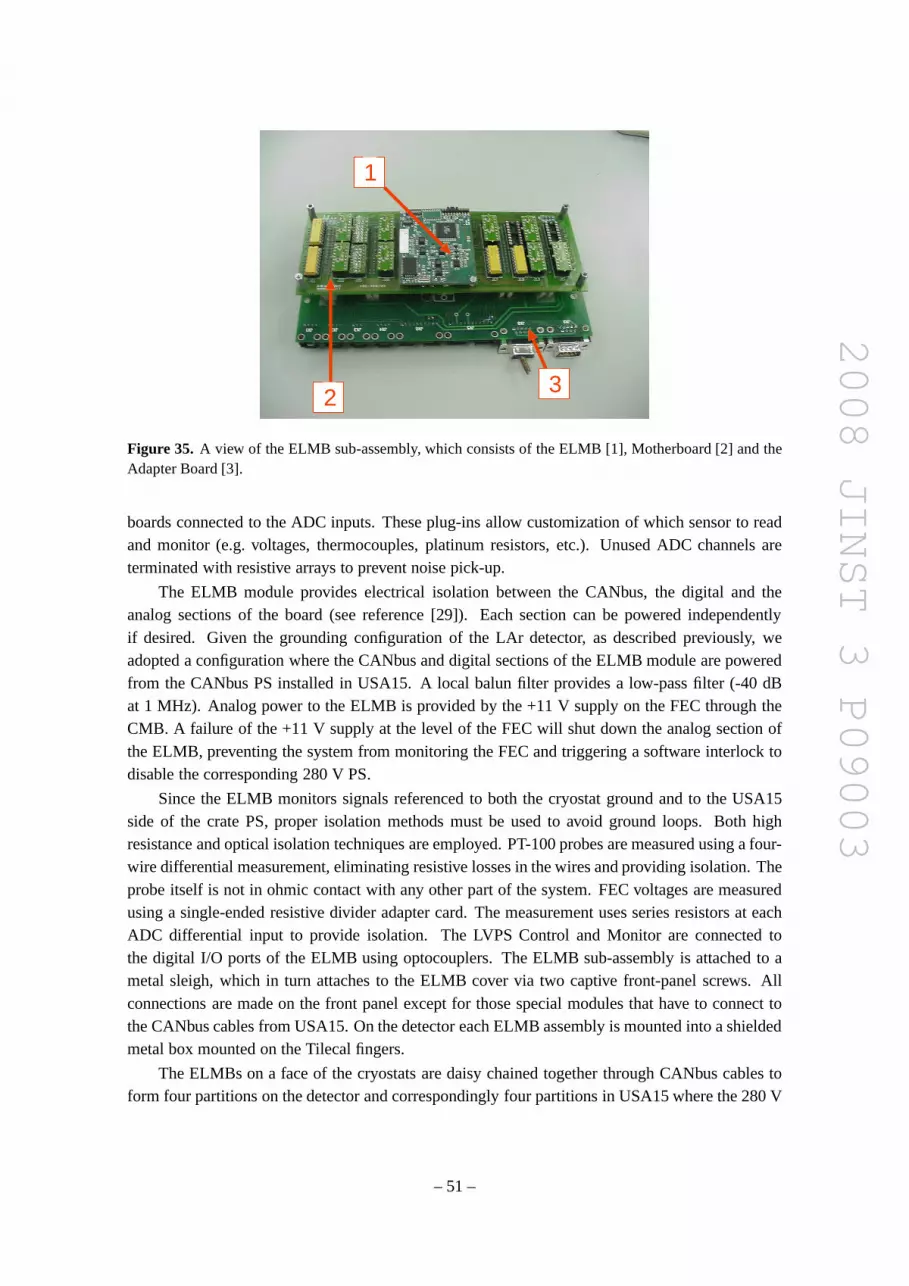
2008 JINST 3 P09003
1
2 3
Figure 35. A view of the ELMB sub-assembly, which consists of the ELMB [1], Motherboard [2] and theAdapter Board [3].
boards connected to the ADC inputs. These plug-ins allow customization of which sensor to readand monitor (e.g. voltages, thermocouples, platinum resistors, etc.). Unused ADC channels areterminated with resistive arrays to prevent noise pick-up.
The ELMB module provides electrical isolation between the CANbus, the digital and theanalog sections of the board (see reference [29]). Each section can be powered independentlyif desired. Given the grounding configuration of the LAr detector, as described previously, weadopted a configuration where the CANbus and digital sections of the ELMB module are poweredfrom the CANbus PS installed in USA15. A local balun filter provides a low-pass filter (-40 dBat 1 MHz). Analog power to the ELMB is provided by the +11 V supply on the FEC through theCMB. A failure of the +11 V supply at the level of the FEC will shut down the analog section ofthe ELMB, preventing the system from monitoring the FEC and triggering a software interlock todisable the corresponding 280 V PS.
Since the ELMB monitors signals referenced to both the cryostat ground and to the USA15side of the crate PS, proper isolation methods must be used toavoid ground loops. Both highresistance and optical isolation techniques are employed.PT-100 probes are measured using a four-wire differential measurement, eliminating resistive losses in the wires and providing isolation. Theprobe itself is not in ohmic contact with any other part of thesystem. FEC voltages are measuredusing a single-ended resistive divider adapter card. The measurement uses series resistors at eachADC differential input to provide isolation. The LVPS Control and Monitor are connected tothe digital I/O ports of the ELMB using optocouplers. The ELMB sub-assembly is attached to ametal sleigh, which in turn attaches to the ELMB cover via twocaptive front-panel screws. Allconnections are made on the front panel except for those special modules that have to connect tothe CANbus cables from USA15. On the detector each ELMB assembly is mounted into a shieldedmetal box mounted on the Tilecal fingers.
The ELMBs on a face of the cryostats are daisy chained together through CANbus cables toform four partitions on the detector and correspondingly four partitions in USA15 where the 280 V
– 51 –

2008 JINST 3 P09003
CAN-A Controller
JunctionBox
Power Supply (+12V)
CAN-B Controller
JunctionBox
Power Supply (+12V)
LARG Calorimeter
One of 16 (13) ELMB Modules
CANbus daisy-chaincable
120Ω
120Ω
USA-15
Figure 36. Loop configuration for the ELMB nodes in a partition on the detector.
power supplies are installed. The ELMBs are connected in a loop configuration which providesthe best protection for the loss of cable connection or the interruption of a cable itself. Two long(70-100 m) cables connect to the loop in opposite positions on the detector side and to the CANbusinterface controllers in the USA15 side (see figure 36). Normally only a single controller is enabledand drives the CANbus. The second controller provides the cable termination and is used as abackup. Signal integrity is preserved, since the loop length is short compared to the total length ofthe transmission lines and the CANbus signals are driven at amaximum frequency of 100 kHz.
A computer located in USA15 acts as the local DCS server for the FECMS. It accesses andsets the state and the configuration of each of the 58 FECs. TheFECMS server is integrated in theoverall ATLAS DCS system and functions as one of the detector’s state machines. Implemented inthis software are the oversight functions for cooling watertemperature and voltages on the FECswhich will shutoff the corresponding 280 V supply should anyof these values go out of the pre-defined acceptable ranges.
– 52 –

2008 JINST 3 P09003
C. Photographs of components of the Front End Crate infrastructure
Figure 37. Photograph of a warm cable used to connect the calorimeter signals from the feedthrough pincarriers to the FEB inputs via the baseplane.
Figure 38. Photograph of a pedestal installed on a detector mockup, with no warm cables installed. Thevacuum lines and pneumatic valves are visible inside the pedestal.
Anderson Powerpole 180I381-SeriesHousing/Spring Assembly
Bussbar laminate
HypertronicsKnurled Socket
M3x18 Dowel Pin
M3x18 Spring Pin
Figure 39. Assembly drawing (left) of a power bussbar and photograph (right) of a bussbar installed on aFEC. The (black) power combs can be seen inserted through thebussbar. The (green) SPAC bus can also beseen, mounted above the power bussbar.
– 53 –

2008 JINST 3 P09003
Figure 40. Photograph of a FEC baseplane for the EMB. The upper and lowerrows of connectors are usedfor input signal connections to the FEBs, and are surroundedby custom springs for improved grounding.The middle row is used for connecting the L1 sums from the FEBsto the TBB/TDB.
Figure 41. Photograph of an optical cable used for transmitting FEB digital readout data from the FEC tothe BE electronics. The fiber ribbons are visible emerging from the outer protective sheath.
Figure 42. Photographs of (left) a cooling plate and (right) a heat transfer plate with thermal pads applied,ready for installation on an FEB.
– 54 –

2008 JINST 3 P09003
Figure 43. Photograph showing racks in USA15 housing the 280 V power supplies.
D. Acronyms used in the paper
ADC - Analog-to-digital converter
ASIC - Application specific integrated circuit
BE - Back end electronics
BNL - Brookhaven National Laboratory
CALIB - Calibration board
CANbus - Controller-area network bus
CMB - Crate monitor board
CONT - Controller board
DAC - Digital-to-analog converter
DCS - Detector control system
DCU - Detector control unit chip for measuring voltages and temperatures
DMILL - Name of radiation hard semiconductor process used for some of the custom ASICs
– 55 –

2008 JINST 3 P09003
DSM - Deep submicron (referring to 0.25µm radiation-tolerant semiconductor process)
DSP - Digital signal processor
EC - Endcap
ELMB - Embedded local monitoring board
EM - Electromagnetic
EMB - Electromagnetic barrel calorimeter
EMEC - Electromagnetic endcap calorimeter
ET - Transverse energy
FCAL - Forward calorimeter
FE - Front end electronics
FEB - Front end board
FEC - Front end crate
FECMS - Front end crate monitoring system
HEC - Hadronic endcap calorimeter
HFEC - Half front end crate
HFFR - Halogen-free, flame-retardant
HVPS - High voltage power supply
I2C - Inter-integrated circuit
L1 - Level 1 trigger
L1CAL - Level 1 calorimeter trigger
LAr - Liquid argon
LHC - Large hadron collider
LSB - Layer sum board
LVPS - Low voltage power supply
MS - Master-to-slave
Opamp - Operational amplifier
PCB - Printed circuit board
PECL - Positive emitter-coupled logic
PLC - Programmable logic controller
PS - Power supply
PSB - Preamplifier summing board of the HEC
ROD - Readout driver board
SCA - Switched-capacitor array analog memory
– 56 –

2008 JINST 3 P09003
SCDB - Serial control daughterboard of the L1 Receiver
SEB - Single event burnout
SM - Slave-to-Master
SMC - Surface-mount component
SPAC - Serial Protocol for ATLAS Calorimeters (serial control system)
TBB - Tower builder board (for the L1 trigger sums of the EM calorimeters)
TDB - Tower driver board (for the L1 trigger sums of the HEC andFCAL)
Tilecal - Scintillator-tile-based hadronic calorimeter
TTC - Trigger, timing and control system
TTCrx - TTC receiver chip
USA15 - Underground service area 15 (off-detector underground counting house)
USB - Universal serial bus
VGA - Variable gain amplifier
References
[1] ATLAS collaboration,ATLAS Technical Proposal for a general-purpose pp experiment at the LargeHadron Collider at CERN, CERN-LHCC-94-43, available athttp://atlasinfo.cern.ch/ATLAS/TP/tp.html.
[2] ATLAS LAr Collaboration,ATLAS Liquid Argon Calorimeter Technical Design Report,CERN-LHCC-96-041, available at http://atlas.web.cern.ch/Atlas/GROUPS/LIQARGEXT/TDR/;B. Aubert et al.,Performance of the ATLAS electromagnetic calorimeter endcap module 0,Nucl. Instrum. Meth.A 500 (2003) 178;B. Aubert et al.,Performance of the ATLAS electromagnetic calorimeter barrel module 0,Nucl. Instrum. Meth.A 500 (2003) 202;J. Colas et al.,Position resolution and particle identification with the ATLAS EM calorimeter,Nucl. Instrum. Meth.A 550 (2005) 96;B. Aubert et al,Construction, assembly and tests of the ATLAS electromagnetic barrel calorimeter,Nucl. Instrum. Meth.A 558 (2006) 388;M. Aharrouche et al.,Energy linearity and resolution of the ATLAS electromagnetic barrelcalorimeter in an electron test-beam, Nucl. Instrum. Meth.A 568 (2006) 601;M. Aharrouche et al.,Response uniformity of the ATLAS liquid argon electromagnetic calorimeter,Nucl. Instrum. Meth.A 582 (2007) 429.
[3] A. Bazan et al.,ATLAS Liquid Argon Calorimeter Back End Electronics, 2007JINST2 P06002.
[4] N.J. Buchanan et al.,Design and implementation of the Front End Board for the readout of the ATLASliquid argon calorimeters, 2008JINST3 P03004.
[5] Details of the ATLAS policy on radiation tolerant electronics can be found athttp://atlas.web.cern.ch/Atlas/GROUPS/FRONTEND/radhard.htm.
[6] M. Dentan et al.,DMILL, a mixed analog-digital radiation-hard BICMOS technology for high energyphysics electronics, IEEE Trans. Nucl. Sci.43 (1996) 1763.
– 57 –

2008 JINST 3 P09003
[7] G. Anelli et al.,Radiation tolerant VLSI circuits in standard deep submicron CMOS technologies forthe LHC experiments: practical design aspects, IEEE Trans. Nucl. Sci.46 (1999) 1690.
[8] Information about the LHC TTC system is available at http://ttc.web.cern.ch/TTC/intro.html.
[9] F. Hubaut et al.,Specifications of the Serial Protocol for the ATLAS LAr Calorimeters: The SPAC3Protocol and Slave ASIC, ATL-AL-ES-0005 (2006), available at https://edms.cern.ch/file/110351/3/.
[10] J. Colas et al.,Electronics Calibration Board for the ATLAS Liquid Argon Calorimeters, submitted forpublication to Nucl. Instrum. Meth.
[11] M. Dhellot et al.,The SPAC Master Module of the LAr Calorimeter Readout Crates,ATL-AL-EN-0064 (2004), available at https://edms.cern.ch/document/478402/1.2.
[12] G. Magazzu, A. Marchioro and P. Moreira,The detector control unit: an ASIC for the monitoring ofthe CMS silicon tracker, IEEE Trans. Nucl. Sci.51 (2004) 1333.
[13] R. Achenbach et al.,The ATLAS Level-1 Calorimeter Trigger, 2008JINST3 P03001.
[14] P. Borgeaud et al.,The ATLAS Tower Builder Board: Calculation, Simulation, Measurements,ATL-AL-EP-0004 (2002), available at https://edms.cern.ch/document/870843/1.
[15] X. de la Broise, A. Le Coguie and J. Schwindling,The Tower Builder Board: Results at the Front EndCrate Test, ATL-AL-TR-0001 (2004), available at https://edms.cern.ch/document/870850/1.
[16] W.E. Cleland et al.,Receiver/Monitor System for the ATLAS Liquid Argon Calorimeters,ATL-AL-EN-0043 (2006), available at https://edms.cern.ch/document/347184/4.
[17] W.E. Cleland,Cabling of the ATLAS Liquid Argon Receiver System, ATL-AL-EN-0042 (2003),available at https://edms.cern.ch/document/347182/2.
[18] L1Cal Group,Cable Mappings and Crate Layouts from Receivers to Processors, ATL-DA-ES-0036(2007), available at https://edms.cern.ch/document/399348/2.
[19] V. Paolone,Remapping Boards for the ATLAS Liquid Argon Receiver System, ATL-AL-EN-0046(2002), available at https://edms.cern.ch/document/366640/3.
[20] W.E. Cleland et al.,Digital Communications in the ATLAS Receiver/Monitor System,ATL-AL-EN-0048 (2003), available at https://edms.cern.ch/document/411279/1.
[21] V. Savinov,Tests of the Receiver/Monitor Stations for the ATLAS Calorimeters: Part 1,ATL-AL-EN-0049 (2003), available at https://edms.cern.ch/document/411281/1.
[22] Application Note OA23, National Semiconductor Corp, available athttp://www.national.com/apnotes/appnotes_all_1.html.
[23] J. Farrell et al.,Description of the LAr Barrel Calorimeter Signal Feedthrough Filter Box,ATL-AB-CD-0001 (2002), available at https://edms.cern.ch/document/344524/1.
[24] M. Dhellot et al.,The Controller Board and SPAC Buses of the ATLAS Liquid ArgonCalorimeterFront End Crates, ATL-AL-EN-0072 (2007), available at https://edms.cern.ch/document/867048/1.
[25] W.E. Cleland,Cabling of the Barrel and EMEC Level 1 Trigger Sums, ATL-AL-ES-0010 (2002),available at https://edms.cern.ch/document/110534/2.
[26] W.E. Cleland,Cabling of the HEC and FCAL Level 1 Trigger Sums, ATL-AL-ES-0017 (2002),available at https://edms.cern.ch/document/347183/1.
[27] G. Mahout et al.,Irradiation studies of multimode optical fibers for use in ATLAS frontend links,Nucl. Instrum. Meth.A 446 (2000) 426.
– 58 –

2008 JINST 3 P09003
[28] B. Arvidsson et al.,A Dense Multi-Ribbon Cable for Installation in a Harsh Environment at CERN,Proceedings of the International Wire and Cable Symposium, Atlantic City (2000).
[29] B. Hallgren et al.,The Embedded Local Monitor Board in the LHC Frontend I/O Control System,Proceedings of the Seventh Workshop on Electronics for LHC Experiments, Stockholm (2001).
[30] A. Barriuso Poy et al.,The detector control system of the ATLAS experiment, 2008JINST3 P05006.
[31] O.C.E.M. S.p.A., Via 2 Agosto 1980, n.11, I-40016 San Giorgio di Piano, Bologna Italy,http://www.ocem.com.
[32] J. Kierstead,PRR of the Liquid Argon Low Voltage Power Supplies, available athttp://indico.cern.ch/conferenceDisplay.py?confId=a04497.
[33] J. Ban et al.,Cold electronics for the liquid argon hadronic endcap calorimeter of ATLAS,Nucl. Instrum. Meth.A 556 (2006) 158.
[34] Iseg Spezialelektronik GmbH, Bautzner Landstr. 23, D-01454 Radeberg / Rossendorf,http://www.iseg-hv.com.
[35] H.M. Braun et al.,Report on Running Channels in ISEG 32-Channel HV Power Supplies, ATLASnote ATL-LARG-PUB-2008-003.
[36] B. Botchev et al.,The high voltage feedthroughs for the ATLAS liquid argon calorimeters,2007JINST2 T10002.
[37] G. Blanchot and L. Hervas,Liquid Argon Installation and Safety Report, ATC-TE-IR-0001 (2004),available at https://edms.cern.ch/document/499605/3.
– 59 –