implementation considerations for “soft” - ubc ece
TRANSCRIPT
IMPLEMENTATION CONSIDERATIONS FOR “SOFT” EMBEDDED PROGRAMMABLE LOGIC CORES
by
James Cheng-Huan Wu
B.A.Sc., University of British Columbia, 2002
A thesis submitted in partial fulfillment of the requirements for
the degree of
Master of Applied Science
in
The Faculty of Graduate Studies
Department of Electrical and Computer Engineering
We accept this thesis as conforming to the required standard:
___________________________
___________________________
___________________________
___________________________
The University of British Columbia
September 2004
© James C.H. Wu, 2004
ii
ABSTRACT
IMPLEMENTATION CONSIDERATIONS FOR “SOFT” EMBEDDED PROGRAMMABLE LOGIC CORES
As integrated circuits become increasingly more complex and expensive, the ability to make
post-fabrication changes will become much more attractive. This ability can be realized using
programmable logic cores. Currently, such cores are available from vendors in the form of
“hard” macro layouts. An alternative approach for fine-grain programmability is possible:
vendors supply an RTL version of their programmable logic fabric that can be synthesized using
standard cells. Although this technique may suffer in terms of speed, density, and power
overhead, the task of integrating such cores is far easier than the task of integrating “hard” cores
into an ASIC or SoC. When the required amount of programmable logic is small, this ease of
use may be more important than the increased overhead. In this thesis, we identify potential
implementation issues associated with such cores, and investigate in depth the area, speed and
power overhead of using this approach. Based on this investigation, we attempt to improve the
performance of programmable cores created in this manner.
Using a test-chip implementation, we identify three main issues: core size selection, I/O
connections, and clock-tree synthesis. Compared to a non-programmable design, the soft core
approach exhibited an average area overhead of 200X, speed overhead of 10X, and power
overhead of 150X. These numbers are high but expected, given that the approach is subject to
limitations of the standard cell library elements of the ASIC flow, which are not optimized for
use with programmable logic.
iii
TABLE OF CONTENTS
ABSTRACT.................................................................................................................................. II
TABLE OF CONTENTS ...........................................................................................................III
LIST OF FIGURES ..................................................................................................................... V
LIST OF TABLES .................................................................................................................... VII
ACKNOWLEDGEMENTS ....................................................................................................VIII
CHAPTER 1 INTRODUCTION.................................................................................................. 1
1.1 MOTIVATION ........................................................................................................................ 1
1.2 RESEARCH GOALS................................................................................................................ 4
1.3 ORGANIZATION OF THE THESIS ........................................................................................... 5
CHAPTER 2 BACKGROUND AND RELEVANT WORK ..................................................... 7
2.1 EMBEDDED PROGRAMMABLE LOGIC CORES FOR SOCS .................................................... 7
2.1.1 Advantages and Design Approaches.............................................................................. 7
2.1.2 General IC Design Flow for SoC Designs................................................................... 10
2.1.3 Design Flow Employing Soft Programmable IPs ........................................................ 14
2.2 OVERVIEW OF SYNTHESIZABLE GRADUAL ARCHITECTURE ............................................ 15
2.2.1 Logic Resources ........................................................................................................... 16
2.2.2 Routing Fabric ............................................................................................................. 17
2.3 CAD FOR SYNTHESIZABLE GRADUAL ARCHITECTURE.................................................... 19
2.3.1 Placement Algorithm.................................................................................................... 20
2.3.2 Routing Algorithm........................................................................................................ 24
2.4 SUMMARY ........................................................................................................................... 25
CHAPTER 3 DESIGN OF A PROOF-OF-CONCEPT PROGRAMMABLE MODULE.... 27
3.1 DESIGN ARCHITECTURE..................................................................................................... 27
3.1.1 Reference Version ........................................................................................................ 28
3.1.2 Programmable Version................................................................................................ 28
iv
3.2 TEST-CHIP IMPLEMENTATION FLOW................................................................................ 29
3.2.1 Modified ASIC IC Design Flow ................................................................................... 30
3.2.2 Front-end IC Design Flow........................................................................................... 31
3.2.3 Back-end IC Design Flow............................................................................................ 33
3.3 DESIGN AND IMPLEMENTATION ISSUES............................................................................. 34
3.3.1 Programmable Core Size Selection ............................................................................. 34
3.3.2 Connections between Programmable Core and Fixed Logic ...................................... 35
3.3.3 Routing the Programmable Clock Signals................................................................... 36
3.4 IMPLEMENTATION RESULTS .............................................................................................. 38
3.4.1 Area Overhead ............................................................................................................. 38
3.4.2 Speed Overhead ........................................................................................................... 41
3.4.3 Validation of Chip on Tester........................................................................................ 42
3.5 SUMMARY ........................................................................................................................... 43
CHAPTER 4 SPEED AND POWER CONSIDERATIONS FOR SOFT-PLC...................... 45
4.1 SPEED CONSIDERATIONS.................................................................................................... 45
4.1.1 Speed Measurement Methodology ............................................................................... 46
4.1.2 Soft-PLC vs. Equivalent ASIC Implementation ........................................................... 49
4.1.3 Speed Improvement Methodology................................................................................ 52
4.1.4 Experimental Results ................................................................................................... 57
4.2 POWER CONSIDERATIONS .................................................................................................. 63
4.2.1 Power Measurement Methodology .............................................................................. 63
4.2.2 Power Overhead vs. Equivalent ASIC Implementation ............................................... 64
4.3 SUMMARY ........................................................................................................................... 67
CHAPTER 5 CONCLUSIONS AND FUTURE WORK ......................................................... 69
5.1 SUMMARY ........................................................................................................................... 69
5.2 FUTURE WORK ................................................................................................................... 71
5.3 CONTRIBUTIONS ................................................................................................................. 72
REFERENCE.............................................................................................................................. 74
v
LIST OF FIGURES
FIGURE 2.1 GENERAL IC DESIGN FLOW [18] ................................................................................. 10
FIGURE 2.2 FLOORPLANNING OF CHIP............................................................................................ 12
FIGURE 2.3 POWER PLANNING ....................................................................................................... 12
FIGURE 2.4 PLACEMENT, AND CLOCK-TREE SYNTHESIS ................................................................. 13
FIGURE 2.5 COMPARISON OF STANDARD FPGA AND SOFT PLC BLOCKS ....................................... 15
FIGURE 2.6 A GENERIC FPGA LOGIC BLOCK.................................................................................. 16
FIGURE 2.7 A LOGIC BLOCK FOR GRADUAL ARCHITECTURE.......................................................... 17
FIGURE 2.8 THE ISLAND-STYLED FPGA ROUTING FABRIC ............................................................. 18
FIGURE 2.9 GRADUAL ARCHITECTURE .......................................................................................... 19
FIGURE 2.10 A GENERIC SIMULATED ANNEALING PSEUDO-CODE [27]............................................ 21
FIGURE 3.1 TEST-CHIP: REFERENCE MODULE ................................................................................ 28
FIGURE 3.2 TEST-CHIP: PROGRAMMABLE MODULE........................................................................ 29
FIGURE 3.3 MODIFIED IC IMPLEMENTATION FLOW ........................................................................ 30
FIGURE 3.4 FUNCTION SIMULATION: (A) CONFIGURATION PHASE (B) NORMAL PHASE.................... 32
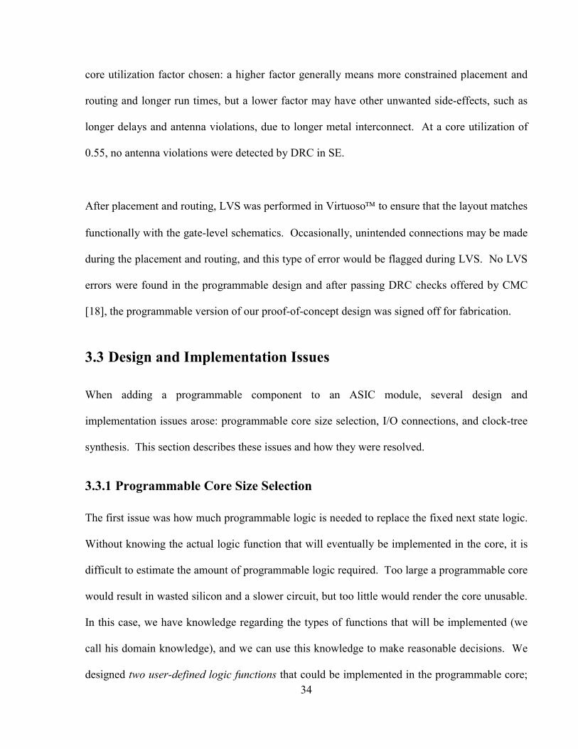
FIGURE 3.5 STATE MACHINE IN SOFT-PLC: (A) 8 STATES, (B) 16 STATES. ...................................... 36
FIGURE 3.6 PROGRAMMABLE CLOCK TREE ROUTING COMPLEXITY ................................................ 37
FIGURE 3.7 LAYOUT OF (A) REFERENCE DESIGN AND (B) PROGRAMMABLE DESIGN ..................... 40
FIGURE 3.8 POST-SYNTHESIS SPEED RESULTS ................................................................................ 41
FIGURE 4.1 SOFT-PLC DELAYS: (A) UN-PROGRAMMED; (B) PROGRAMMED ................................... 47
FIGURE 4.2 STATIC TIMING ANALYSIS FLOW: FUNCTIONAL DELAY................................................ 47
FIGURE 4.3 SETTING LOGIC VALUE (0/1) ON FFS FOR A LUT......................................................... 48
FIGURE 4.4 SETTING CORRECT PATHS BY DISABLING FALSE PATHS................................................ 49
vi
FIGURE 4.5 GRADUAL ARCHITECTURE: (A) LOGICAL VIEW; (B) PHYSICAL VIEW ........................... 53
FIGURE 4.6 INTER-CLB DELAYS: (A) LOGICAL VIEW; (B) PHYSICAL VIEW..................................... 54
FIGURE 4.7 CONNECTION DELAY LOOKUP: A) ORIGINAL; B) PROPOSED ......................................... 56
FIGURE 4.8 SPEED IMPROVEMENT + SPEED MEASUREMENT FLOW.................................................. 57
FIGURE 4.9 EXPERIMENTAL RESULTS: % CHANGE VS. TIMING TRADEOFF PARAMETER.................. 60
FIGURE 4.10 HISTOGRAM: A) SUB-BLOCKS; B) INTERCONNECT WIRES .......................................... 61
FIGURE 4.11 DELAY OF LEVEL 1&2 SOURCE TO LEVEL N SINK ...................................................... 62
FIGURE 4.12 POWER ANALYSIS FLOW: A) ASIC; B) SOFT-PLC...................................................... 64
FIGURE 4.13 POWER DISTRIBUTION OF SOFT-PLCS........................................................................ 66
FIGURE 4.14 CONFIGURATION MODULE OF SOFT-PLC ................................................................... 67
vii
LIST OF TABLES
TABLE 3.1 POST-SYNTHESIS AREA AND GATE COUNT SUMMERY ................................................. 39
TABLE 3.2 POST-LAYOUT AREA SUMMARY................................................................................... 39
TABLE 3.3 POST-LAYOUT SPEED RESULTS .................................................................................... 42
TABLE 3.4 SPEED MEASUREMENTS: SIMULATION SPEED VS. MEASURED SPEED........................... 42
TABLE 3.5 OFF-CHIP POWER MEASUREMENTS............................................................................... 43
TABLE 4.1 ASIC SYNTHESIS AND PHYSICAL DESIGN RESULTS ..................................................... 50
TABLE 4.2 SOFT-PLC SYNTHESIS AND PHYSICAL DESIGN RESULTS.............................................. 50
TABLE 4.3 AREA/SPEED COMPARISON OF SOFT-PLC TO ASIC ..................................................... 51
TABLE 4.4 EXPERIMENT A: COMPLEX NET EXTRACTION.............................................................. 58
TABLE 4.5 EXPERIMENT B: SIMPLIFIED NET EXTRACTION............................................................ 59
TABLE 4.6 EXPERIMENT C: CONSTANT DELAY ASSIGNMENT ....................................................... 59
TABLE 4.7 POWER SIMULATION RESULTS FOR ASIC IMPLEMENTATION ....................................... 64
TABLE 4.8 POWER SIMULATION RESULTS FOR SOFT-PLC IMPLEMENTATION................................ 65

viii
ACKNOWLEDGEMENTS
First of all, I would like to thank my two academic supervisors, Dr. Resve Saleh and Dr. Steve
Wilton, for their guidance, technical advice, and moral support that they have provided
throughout my Masters. From them, I have learned a great deal about how to conduct and
present research; they have enabled me to think critically not only from a technical perspective
but also from a broader point of view.
I would also like to thank other members of the SoC research group: Andy Yan, Anthony Yu,
Brad Quinton, Eddy Lee, Julien Lamoureux, Kimberly Bozman, Martin Ma, Marvin Tom, Noha
Kafafi, Victor Aken’Ova, and Zion Kwok. Their thoughtful insights and advice are much
appreciated. Special thanks are due to Kim and Noha, for their ground work on Soft-PLC; to
Victor and Julien, for their expertise in CAD tools; to Dr. Guy Lemieux, for his helpful technical
advice; and to the SoC staff, for making the lab a more comfortable place to work.
I greatly appreciate the financial support provided by Altera Corporation, Micronet R&D, the
Natural Science and Engineering Council of Canada (NSERC), and PMC-Sierra. I would also
like to thank Canadian Microelectronics Corporation (CMC) for providing the CAD tools, as
well as fabrication and test facilities.
Finally, I would especially like to thank my parents and my sister, Winnie, for their support and
encouragement throughout my years of education, and Teresa Su for her patience and continual
support.
1
Chapter 1
Introduction
1.1 Motivation
Over the past 30 years, we have witnessed impressive improvements in the achievable density of
integrated circuits (IC) [1]. In order to maintain this rate of improvement, designers need new
techniques to manage the increased complexity inherent in these large chips. One such emerging
technique is the System-on-a-Chip (SoC) design methodology. In this methodology, pre-
designed and pre-verified blocks, often called intellectual property (IP), are obtained from
internal sources or third-parties, and combined on a single chip. These cores may include
embedded processors, memory blocks, interface blocks and components that handle application
specific processing functions. Large productivity gains can be achieved using this approach. In
fact, rather than implementing each of these components separately, the role of the SoC designer
is to integrate them onto a chip to implement complex functions in a relatively short amount of
time.
One major issue today in SoC design is the overall design cost in terms of engineering costs, the
cost of IP blocks and the rising costs of masks in advanced technologies. In 1986, Intel’s first
150µm factory was built and filled with manufacturing equipment for just over $25 Million; in
2
2002, a typical exposure tool for 90nm technology alone can cost $12M, and for 45nm and
below the forecasted cost is as high as $20M [2]. This has led to the rising costs of masks: a
mask set averages $750,000 for a 130nm design, $1.5M for a 90nm design, and $3.0M projected
for a 65nm design [3]. Therefore, the cost of errors in the design can become significant. No
matter how seamless the SoC design flow is made, and no matter how careful an SoC designer is,
there will inevitably be some chips that have problems that are found after fabrication. “Re-
spinning” of the chip will take months, and this leads to higher development costs, increased
time-to-market, and perhaps a lost market opportunity.
One solution is to implement the entire SoC on Field Programmable Gate Arrays (FPGAs).
FPGAs are pre-fabricated integrated circuits that can be programmed to implement virtually any
logic functions after fabrication [3]. This approach eliminates the need for fabrication of fully
custom ASIC1 designs, and any errors or changes in design requirements can be easily re-
programmed onto FPGA. However, FPGAs suffer in terms of area, speed, and power, when
compared to equivalent ASIC implementation. According to one company that specializes in
configurable logic, in a 0.18 µm technology, circuitry implemented in an FPGA is about 40
times less dense, 6 times slower, and consumes 30 times more power, than standard cell
implementation [5]. In many cases, FPGAs do not meet the speed and power requirements, but
they play an important role in product prototyping and low-volume products.
1 ASIC is an industry term that refers to application-specific integrated circuits that are created using a well-established design flow involving standard cells.
3
One school of thought is to combine the flexibility of an FPGA and the performance of an ASIC
to deliver an SoC platform that is cost-effective and meets time-to-market constraints. Evolving
standards can be mapped onto one or more programmable IPs, while logic that is unlikely to
change can be implemented as fixed functional blocks. Furthermore, product differentiation is
key to survival for companies competing in the same market segment; the ability to quickly
customize a product to hit moving target specifications becomes increasingly important. For
these reasons, it is desirable to construct SoCs with embedded programmable cores, to amortize
the cost of a single design across many related applications.
Despite the compelling advantages, the use of programmable logic cores in SoCs has not become
mainstream. In fact, many companies that develop these cores have changed their focus
[5][6][7][8]. There are a number of reasons for this [9]. One reason is that designers often find
it difficult to identify a subsystem that can be easily implemented in programmable logic. A
second reason is that embedding a core with an unknown function makes timing, power
distribution, and verification difficult. This extra design complexity limits the use of
programmable logic cores to certain applications.
In [10], an alternative technique is described which speaks to the second of these concerns. In
this technique, core vendors supply a synthesizable version of their programmable logic core (a
“soft” core) and the integrated circuit designer synthesizes the programmable logic fabric using
standard cells. Although this technique may have disadvantages in terms of speed, density, and
power, the task of integrating such cores is far easier than the task of integrating “hard” cores
4
into a fixed-function chip. For very small amounts2 of logic, this ease of use may be more
important than the increased overhead. This thesis addresses a number of practical issues
associated with the “soft” programmable logic core approach.
1.2 Research Goals
In prior research work, an investigation into various architectures and CAD algorithms for the
synthesizable programmable logic core (soft-PLC) approach was carried out. The goal of the
research described here is to validate the feasibility of including such logic cores in an SoC; this
is achieved by implementing a test-chip that contains an embedded soft-PLC that interacts with
the fixed logic portion of the chip. In addition, we investigate area, speed and power overhead of
implementing user circuits on soft-PLCs versus implementing them as fixed-logic using standard
cells. Specifically, the purpose of this thesis is to answer the following questions:
1. Can we use existing ASIC CAD tools and IC design flow to implement a chip that
contains both fixed and synthesizable programmable logic? What kind of
implementation issues arise when a piece of soft-PLC is incorporated into an SoC design?
2. What are the area, speed and power scaling factors when implementing user circuits on a
soft-PLC versus implementing the same circuits on fixed ASIC logic? How can the
performance of soft-PLCs be further improved?
2 Here we consider the small amount as in the range of a hundred equivalent ASIC gates. Please refer to Section 3.2.1 for more detail.
5
Thus, the primary goal is to evaluate whether synthesizable embedded programmable logic cores
are a viable alternative to hard-core embedded FPGAs. The issues are addressed through
physical implementation of a test chip containing such a core. We identify potential
shortcomings of soft-PLC approach, and then develop methods to further improve the
performance of soft-PLCs.
The contributions of this thesis are summarized as follows:
1. Implemented a test-chip containing fixed logic (implemented using a standard ASIC
design flow) and programmable logic (implemented using the soft-PLC approach).
2. Identified implementation issues that arose during the implementation of the test-chip
throughout the entire IC design flow. The fabricated test-chip has been functionally
tested to validate the concept of soft-PLC.
3. Obtained speed and power consumption estimates of soft-PLCs using a simulation-based
approach, and evaluated the performance and power overhead relative to purely fixed
ASIC implementations.
4. Developed a new technique to enhance the performance of soft-PLC.
1.3 Organization of the Thesis
Chapter 2 provides an overview of Embedded Programmable Logic Cores for System-on-a-Chip
(SoC) platform. It contrasts the concept of synthesizable programmable logic cores with a more
conventional approach. It also describes previous work done in the area of synthesizable
programmable logic cores and the CAD algorithms used to map user circuits onto this IP.
6
Chapter 3 describes the goal of this research which is to validate the concept of synthesizable
programmable logic cores by implementing a physical chip that contains both fixed and
programmable logic, and to understand any implementation issues that may arise during the IC
design flow, from RTL to physical layout. The fabricated chip is then tested for functionality to
complete the investigation.
Chapter 4 describes the performance and power implications of implementing a user-defined
circuit on a synthesizable programmable logic core, compared to implementing the same user-
defined circuit on fixed ASIC logic. Understanding the speed overhead, we seek ways to
optimize the performance without compromising the ease of use of the soft-core approach. To
this end, we have developed a new CAD technique that may help enhance the soft-core
performance. Using standard ASIC CAD tools, we determine the gains of our performance
enhancement technique.
Chapter 5 provides a brief summary of the work, directions for future research and a list of the
contributions.
7
Chapter 2
Background and Relevant Work
This chapter begins with an overview of Embedded Programmable Logic Cores for System-on-a-
Chip (SoC) platform. Specifically, it describes the concept of synthesizable programmable logic
cores and contrasts this idea to a more conventional approach. It then describes previous work
done in the area of synthesizable programmable logic cores; in particular, it discusses the
architecture of a synthesizable programmable IP and the CAD algorithms used to map user
circuits onto this IP.
2.1 Embedded Programmable Logic Cores for SoCs
The System-on-Chip design flow allows system designers to integrate various kinds of third-
party Intellectual Property onto a singe chip. In this flow, system designers obtain pre-verified IP
blocks from various suppliers that specialize in the design of IPs used in different areas, and
integrate them. As a result, the design and verification time, which directly translates to time-to-
market, is significantly reduced.
2.1.1 Advantages and Design Approaches
Incorporating an embedded programmable IP in SoC-style design has many advantages [11]:
1. Rapid development with some design details that can be incorporated into the
programmable portion of the chip.
8
2. Amortization of design cost over a family of products based on the same platform but
differentiated by the content of the programmable portion of the chip.
3. Possibility of product upgrades within the programmable portion of the chip.
4. Provision of test access mechanism to various parts of the chip.
These advantages have prompted several designers to employ embedded programmable IPs in
their SoC designs [12][13][14].
Currently, there are several commercially available embedded programmable IPs that can be
loosely categorized into two types: SRAM-based FPGAs [5][7][8] and mask-programmable
logic cores [6]. Normally, these cores are available in the form of physical layout information,
stored in data exchange format (DEF) files. Some products, such as eASICore[5], offer
flexible configuration of the basic logic blocks for the targeted applications, but most embedded
programmable IPs are made available in fixed sizes and shapes. These are commonly referred to
as hard cores.
In either case, the integration process can be cumbersome for most designers: new CAD tools
need to be learned, and there is little or no visibility to the internal structure of the programmable
IP at the transistor level. A programmable IP acquired from a third-party vendor must be
designed with the same set technology library and design rules as the rest of the design. To
ensure the programmable IP is compliant with the foundry’s processing requirements, the IP
should be fabricated and characterized at least once before it is put to use.
9
To address the design issues associated with this “hard” core approach described above, a novel
design methodology was proposed in [15]. In this new scheme, the designer receives the core in
the form of a “soft” core. A “soft” core is one in which the designer obtains an RTL description
of the behavior of the core, written in Verilog or VHDL. In this sense, it is similar to the
definition of a soft IP core used in SoC designs [16]. The distinction is that, in a soft PLC, the
user circuit to be implemented in the core is programmed after fabrication.
The value of this approach is derived from the tools needed to implement the fabric. Since the
designer receives only an RTL description of the behavior of the core, CAD tools must be used
to map the behavior to gates and eventually to layout. These tools can be the same ones that are
used to in the standard ASIC flow. In fact, the primary advantage of this novel approach is that
existing ASIC tools can be used to implement the programmable core. No modifications to the
tools are required, and the flow follows a standard integrated circuit design flow. This will
significantly reduce the design time of chips containing these cores.
A second advantage is that this technique allows small blocks of programmable logic to be
positioned very close to the fixed logic that connects to the programmable logic to improve
routability and shorten wire lengths. The use of a “hard” core requires that all the programmable
logic be grouped into a small number of relatively large blocks. A third advantage is that the
new technique allows users to customize the programmable logic core to better support the target
application. This is because the description of the behavior of the programmable logic core is an
RTL description that can be easily understood and edited by the user. Finally, it is a simple
10
matter to migrate the programmable block to new technologies; new programmable logic cores
from the core vendors are not required for each technology node.
Of course, the main disadvantage of the proposed technique is that the area, power, and speed
overhead will be significantly increased, compared to implementing programmable logic using a
“hard” core. Thus, for large amounts of circuitry, this technique would not be suitable. It only
makes sense if the amount of programmable logic required is small. We will quantify the area,
timing and power tradeoffs in the later chapters, but first we explore the issues of design flow
and architecture suitable for such an approach.
2.1.2 General IC Design Flow for SoC Designs
The basic IC design flow can be decomposed into two phases: front-end synthesis, and back-end
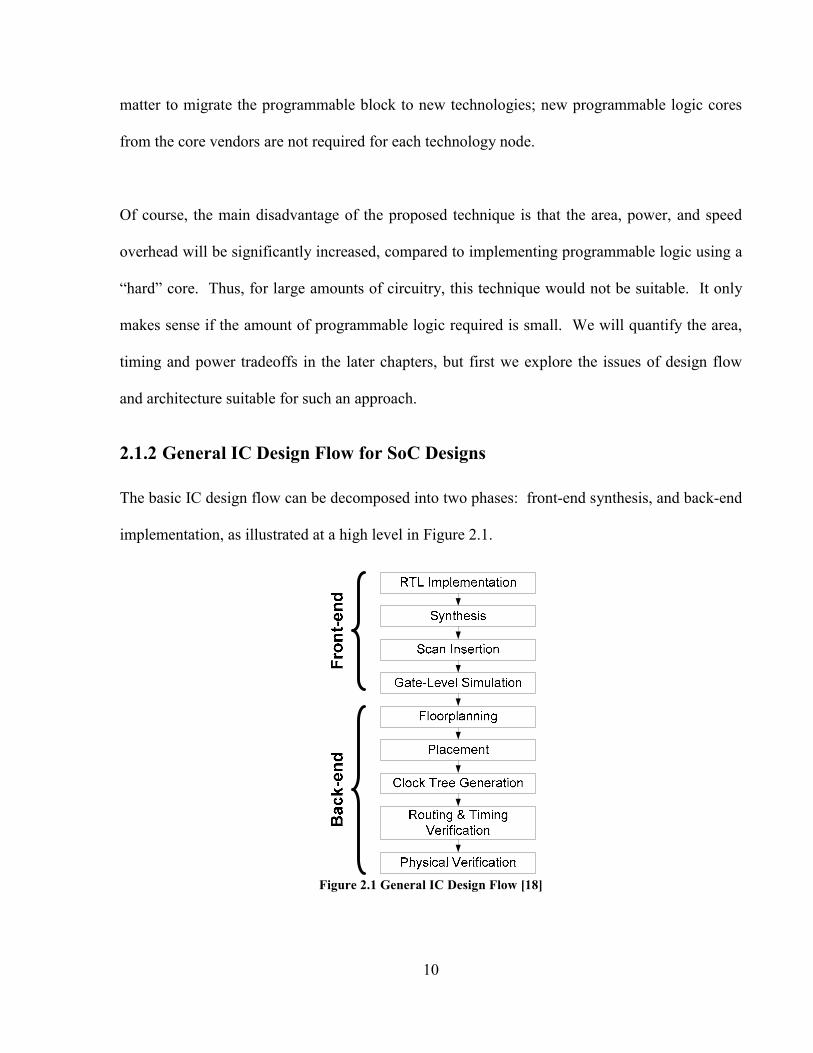
implementation, as illustrated at a high level in Figure 2.1.
Figure 2.1 General IC Design Flow [18]
11
Although Figure 2.1 shows a series of steps executed sequentially, the actual IC design flow is an
iterative process where the designers may be required to perform synthesis multiple times in
order to obtain desired timing closure.
The IC design flow starts with register-transfer-level (RTL) implementation: the designer
describes at an abstract level the hardware circuitries and their interconnections using an HDL
language such as VHDL or Verilog [16]. The RTL must be written such that the design is
synthesizable [19], meaning that a specific subset of the RTL language must be used to define
the blocks so that it can be easily translated and mapped to standard cells3. Several electronic
design automation (EDA) companies offer synthesis tools [20][21][22], and one used in this
thesis is the Design Compiler from Synopsys, Inc [19]. Once a design is synthesized into gate-
level netlist, design-for-test (DFT) techniques are applied to the design; a basic DFT technique is
to implement scan chains using the existing flip-flops. The gate-level design is then verified
through the use of functional simulation. Once the design is fully verified and meets the timing
specifications, the front-end synthesis is considered to be complete.
Back-end implementation concerns with the physical aspect of the design; this part of IC flow is
completed with the aid of Cadence tools [21]: Physical Design Planner, First Encounter,
Silicon Ensemble, and Virtuoso. During the floorplanning stage, the designer manually
places each module within the core area; a module can be a gate-level block from synthesis, or a
3 Both VHDL and Verilog contain a rich set of language constructs, but not all features can be easily converted to logic gates. Therefore, a synthesizable subset has been defined that will guarantee that logic synthesis can be applied.
12
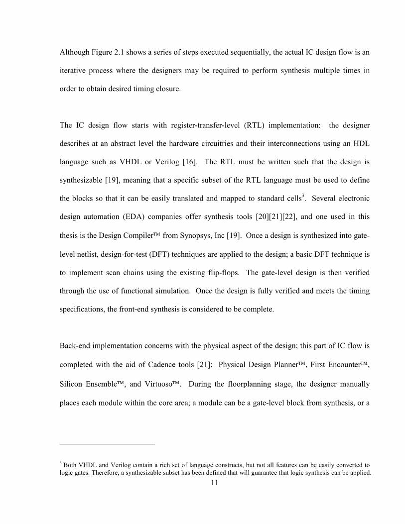
black-box macro from a third-party vendor, such as the hard-core FPGA block illustrated in
Figure 2.2 .
Figure 2.2 Floorplanning of Chip
After the location of each module is defined, the designer can create power grids to distribute
VDD and VSS (or ground) to the standard cells and the black-box IPs. Basic power planning
includes power rings and power stripes, each of which comes in a pair of VDD and VSS power
line, as illustrated in Figure 2.3
Figure 2.3 Power Planning
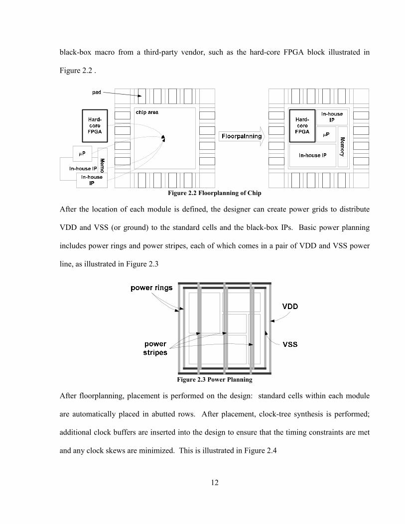
After floorplanning, placement is performed on the design: standard cells within each module
are automatically placed in abutted rows. After placement, clock-tree synthesis is performed;
additional clock buffers are inserted into the design to ensure that the timing constraints are met
and any clock skews are minimized. This is illustrated in Figure 2.4
13
Figure 2.4 Placement, and clock-tree synthesis
All the tasks described so far can be accomplished in Physical Design Planner or First
Encounter tool. Then, the design is ported to Silicon Ensemble for power routing and signal
routing; this process can be automated, if desired. At this point, the layout is verified against
geometry design rules and antenna violations4 to ensure the design is properly placed, routed,
and free of open connections. After routing, timing verification is performed; timing verification
checks the routed design against the timing constraints for possible setup and hold-time
violations. This process can be performed in PEARL or PrimeTime tool. After timing
verification, the design is ready for physical verification: the layout is checked against the
schematics to ensure they are functionally identical. This process is called layout-vs-schematics
(LVS), and is performed in Virtuoso. Once LVS has passed, the layout is ready for a final
design-rule-check (DRC) and sign-off for fabrication. The final layout is stored in the GDSII
4 Antenna effect refers to a phenomenon in which charge is attracted to each metal layer like an antenna. When too much charge accumulates on a gate, the transistor can be damaged by shortening the gate to the substrate; longer interconnects have larger surface area and therefore, tend to attract more charges [49]. An antenna violation occurs when the ratio of metal area over gate area exceed certain threshold set by the design-rule check (DRC), and this is flagged as a potential antenna effect.
14
format, which specifies the layout geometry in 2-D coordinates. Delivering the design in this
format to the foundry is called tapeout.
2.1.3 Design Flow Employing Soft Programmable IPs
Based on the general IC design flow, we now describe how this flow can be used for
synthesizable programmable logic cores (soft-PLCs). The main steps are as follows:
1. The integrated circuit designer partitions the design into functions that will be
implemented using fixed logic and programmable logic, and describes the fixed functions
using a hardware description language. At this stage, the designer must determine the
size of the largest function that will be supported by the core; this can be done either by
considering example configurations, or based on the experience of the designer.
2. The designer obtains an RTL description of the behavior of a programmable logic core.
This behavior is also specified in the same hardware description language.
3. The designer merges the behavioral description of the fixed part of the integrated circuit
(from Step 1) and the behavioral description of the programmable logic core (from Step
2), creating a behavioral description of the block.
4. Standard ASIC design flow for synthesis, place, and route tools is then used to implement
the soft PLC behavioral description from Step 3. In this way, both the programmable
logic core and fixed logic are implemented simultaneously.
5. The integrated circuit is fabricated.
6. The user configures the programmable logic core for the target application.
Note that in Step 4 of the design flow, there is an important difference in the implementation of
the programmable logic for a hard FPGA fabric and a soft PLC fabric, as illustrated in Figure 2.5.
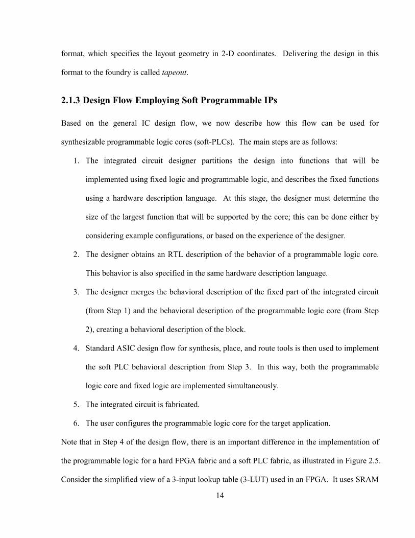
Consider the simplified view of a 3-input lookup table (3-LUT) used in an FPGA. It uses SRAM
15
cells to store configuration bits and pass transistors to implement the 3-LUT shown in Figure
2.5(a). In the soft PLC case, shown in Figure 2.5(b), a standard-cell library is used to implement
the same 3-LUT. In fact, all desired functions of the soft PLC are constructed from NANDs,
NORs, inverters, flip-flops (FF) and multiplexers from the standard cell library. The same holds
true for the programmable interconnect in the soft PLC.
Figure 2.5 Comparison of standard FPGA and soft PLC blocks
To emphasize this point further, consider how the complete fabric would be constructed in the
two cases. For the soft PLC, the final logic schematic and layout is determined by the logic
synthesis tool, technology mapping algorithms, and the place-and-route tool. In the case of a
hard fabric, a custom layout approach is used to create a “tile” for the FPGA. Then the FPGA
fabric is assembled by replicating the tiles horizontally and vertically. Clearly, the standard
FPGA approach is more area efficient but the soft PLC has the advantage of ease of use.
2.2 Overview of Synthesizable Gradual Architecture
Up to this point, the soft-PLC approach has been described, but the actual architecture of the
fabric has not been addressed. Since the soft-PLC is intended for small applications, its
architecture is expected to differ from standard FPGAs. In fact, several alternative architectures
16
for a soft programmable logic core have been proposed. Three LUT-based architectures have
been proposed in [15]: Directional, Gradual and Segmented. Also, a product-term-block (PTB)
based architecture has been proposed in [17]. Based on the findings in [15], the Gradual
Architecture was shown to be the most area efficient LUT-based architecture and thus, it has
been chosen as the reference architecture for our research experiments.
2.2.1 Logic Resources
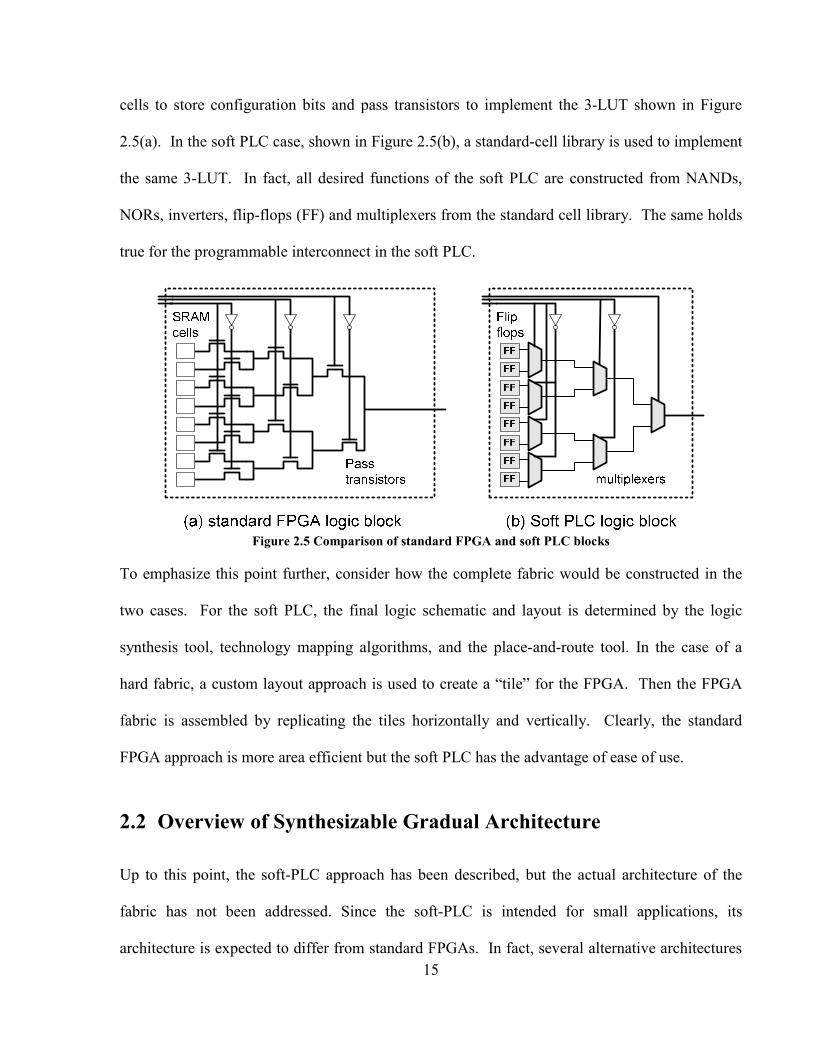
Logic blocks implement the logical component of a user circuit. Most commercial FPGAs use
K-input lookup-tables (K-LUT) as the basic logic blocks. A K-LUT can implement any K-input
functions and requires 2K configuration bits. As an example, Figure 2.5 illustrates the topology
of a 3-LUT. Historically, it has been understood that 4=K results in most efficient FPGAs
[23][24]. Recent FPGA developments indicate the successful use of larger look-up tables that
can implement up to 7-input functions [25]. In early FPGAs, a K-LUT, a flip-flop (FF), and an
output select multiplexer formed a logic module called logic element (LE). A standard FPGA
now has several logic elements grouped together to form a cluster; a diagram detailing the entire
logic structure with N clusters is shown in Figure 2.6.
Figure 2.6 A generic FPGA logic block
17
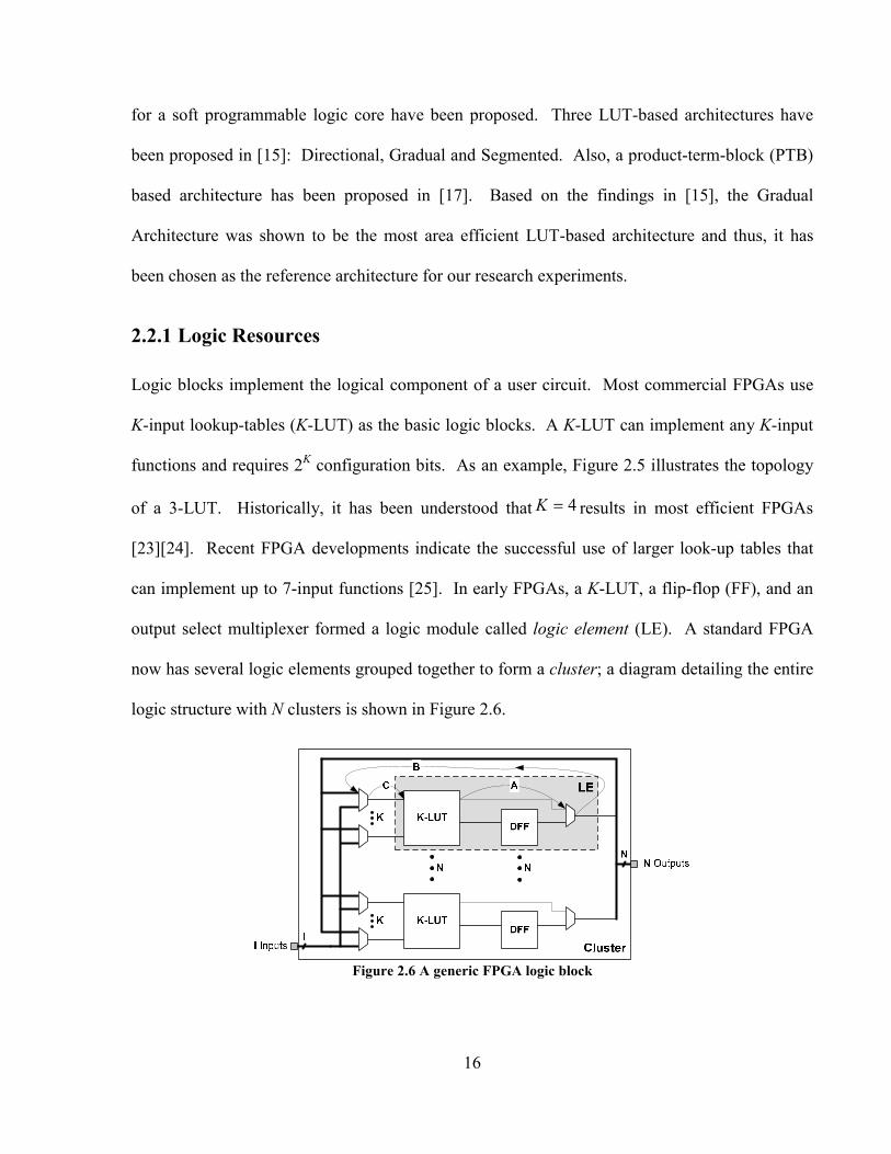
Similar to most commercial FPGAs, the Gradual Architecture uses LUT-based logic resources.
It had been demonstrated experimentally that 3=K results in the most area-efficient Gradual
Architecture [15]. Since soft-PLC only makes sense for very small amount of programmable
logic, an envisaged application would be the next state logic in a state machine. In that case,
only combinational functions need to be mapped onto the programmable cores, and the structure
of a logic block can be further simplified. Therefore, the cluster structure is reduced to just a
single LE, with the FF, the local connection switches, and the output select multiplexer removed
from the LE as well. This helps reduce the area overhead and removes a possible combinational
loop shown by the path labeled A, B and C in Figure 2.6. Although this combinational loop
should not exist after programming, it can cause many CAD tools to perform inaccurate timing
analysis during various stages of the IC design flow. The simplified logic structure for the
Gradual Architecture is shown in Figure 2.7; the cluster now contains just a single 3-LUT.
Figure 2.7 A logic block for Gradual Architecture
2.2.2 Routing Fabric
In FPGAs, the routing fabric connects the internal components such as logic blocks and I/O
blocks. The routing fabric is comprised of three main components: wire segments, connection
blocks, and switch blocks. As illustrated in Figure 2.8, wire segments form the routing channels,
connection blocks connect the routing channels and the logic blocks, and the switch blocks
connect the intersecting vertical and horizontal routing channels.
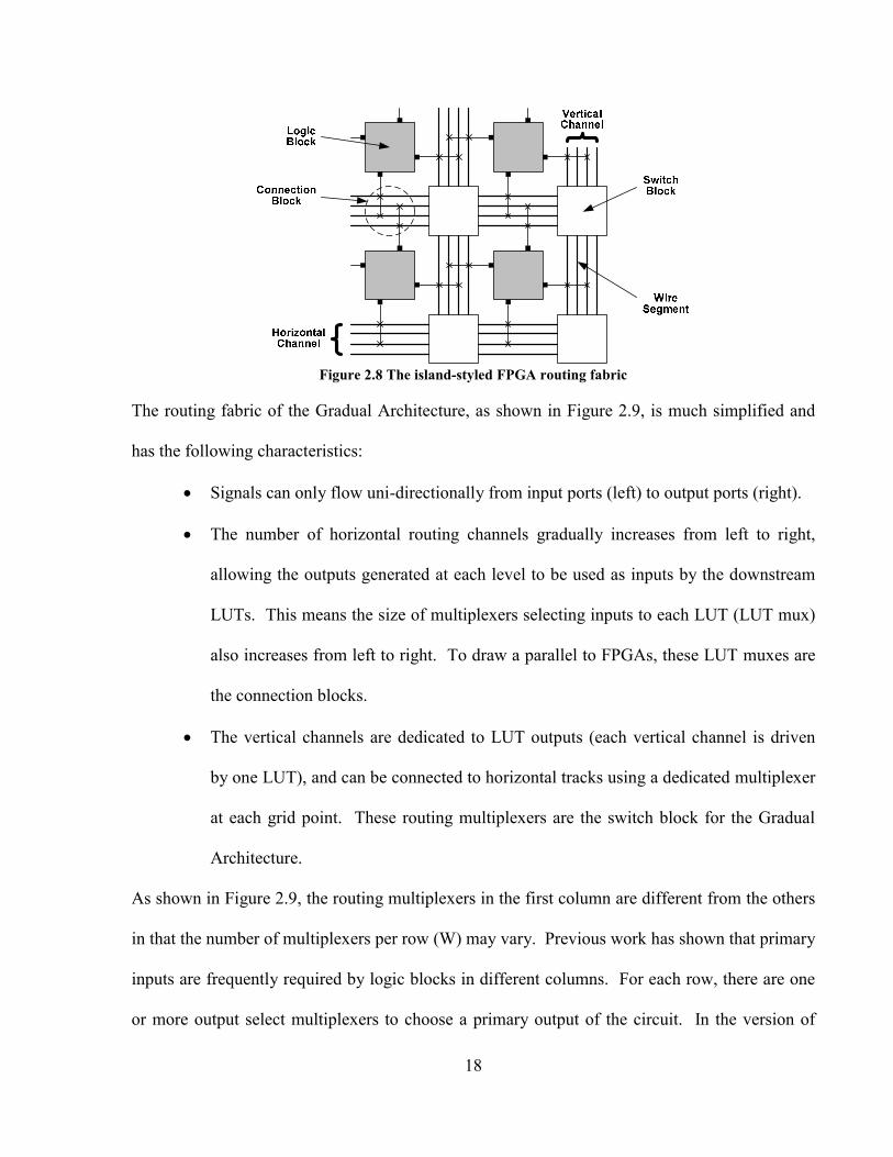
18
Figure 2.8 The island-styled FPGA routing fabric
The routing fabric of the Gradual Architecture, as shown in Figure 2.9, is much simplified and
has the following characteristics:
• Signals can only flow uni-directionally from input ports (left) to output ports (right).
• The number of horizontal routing channels gradually increases from left to right,
allowing the outputs generated at each level to be used as inputs by the downstream
LUTs. This means the size of multiplexers selecting inputs to each LUT (LUT mux)
also increases from left to right. To draw a parallel to FPGAs, these LUT muxes are
the connection blocks.
• The vertical channels are dedicated to LUT outputs (each vertical channel is driven
by one LUT), and can be connected to horizontal tracks using a dedicated multiplexer
at each grid point. These routing multiplexers are the switch block for the Gradual
Architecture.
As shown in Figure 2.9, the routing multiplexers in the first column are different from the others
in that the number of multiplexers per row (W) may vary. Previous work has shown that primary
inputs are frequently required by logic blocks in different columns. For each row, there are one
or more output select multiplexers to choose a primary output of the circuit. In the version of
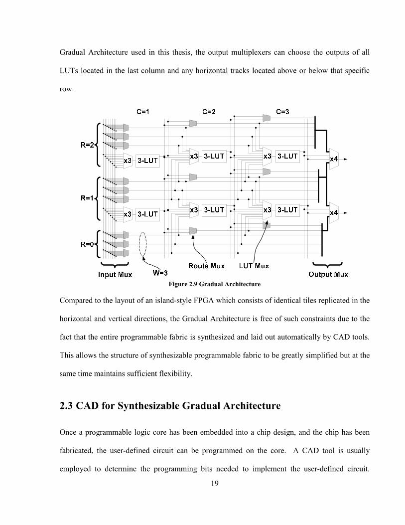
19
Gradual Architecture used in this thesis, the output multiplexers can choose the outputs of all
LUTs located in the last column and any horizontal tracks located above or below that specific
row.
Figure 2.9 Gradual Architecture
Compared to the layout of an island-style FPGA which consists of identical tiles replicated in the
horizontal and vertical directions, the Gradual Architecture is free of such constraints due to the
fact that the entire programmable fabric is synthesized and laid out automatically by CAD tools.
This allows the structure of synthesizable programmable fabric to be greatly simplified but at the
same time maintains sufficient flexibility.
2.3 CAD for Synthesizable Gradual Architecture
Once a programmable logic core has been embedded into a chip design, and the chip has been
fabricated, the user-defined circuit can be programmed on the core. A CAD tool is usually
employed to determine the programming bits needed to implement the user-defined circuit.
20
Since our architectures contain novel routing structures, some modifications must be made to
standard FPGA placement and routing algorithms. This section describes these modifications for
the Gradual Architecture described in the previous section.
It is important to note that we are not referring to the standard cell placement and routing tools
needed to implement the programmable fabric itself onto the chip. Rather, the algorithms in this
section are used to implement a user circuit on the programmable fabric after the chip has been
fabricated. For example, the Versatile Place and Route (VPR) tool [26][27] determines where to
place the logic functions and how to form the connections between the logic functions on a given
FPGA fabric. At the end of the process, the programming bits are generated for the fabric.
These bits must be shifted into flip-flops of the fabricated chip to implement a user-defined
circuit. The process is repeated if a different user circuit is to be implemented.
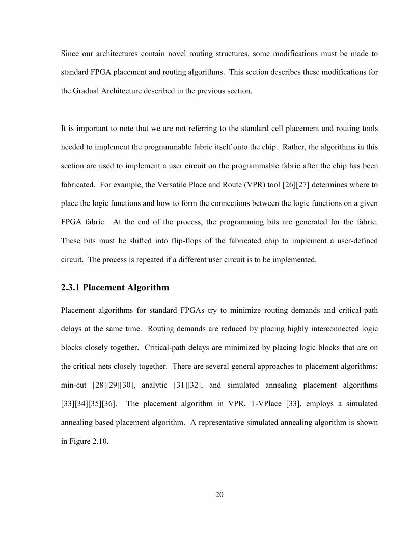
2.3.1 Placement Algorithm
Placement algorithms for standard FPGAs try to minimize routing demands and critical-path
delays at the same time. Routing demands are reduced by placing highly interconnected logic
blocks closely together. Critical-path delays are minimized by placing logic blocks that are on
the critical nets closely together. There are several general approaches to placement algorithms:
min-cut [28][29][30], analytic [31][32], and simulated annealing placement algorithms
[33][34][35][36]. The placement algorithm in VPR, T-VPlace [33], employs a simulated
annealing based placement algorithm. A representative simulated annealing algorithm is shown
in Figure 2.10.
21
T = InitialTemperature();
S = RandomPlacement();
Rlimit = InitialRlimit();
while(ExitCriterion() == False) { /* Outer Loop */
while(InnerLoopCriterion() == False) { /* Inner Loop */
Snew = GenerateViaMove(S, Rlimit);
∆C = Cost(Snew) - Cost(S);
r = random(0, 1);
if (r < exp(-∆C/T))
S = Snew; /* accept swap */
}
T = UpdateTemp(); /* cool down */
Rlimit = UpdateRlimit();
}
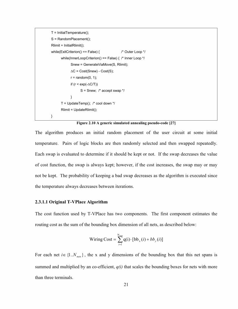
Figure 2.10 A generic simulated annealing pseudo-code [27]
The algorithm produces an initial random placement of the user circuit at some initial
temperature. Pairs of logic blocks are then randomly selected and then swapped repeatedly.
Each swap is evaluated to determine if it should be kept or not. If the swap decreases the value
of cost function, the swap is always kept; however, if the cost increases, the swap may or may
not be kept. The probability of keeping a bad swap decreases as the algorithm is executed since
the temperature always decreases between iterations.
2.3.1.1 Original T-VPlace Algorithm
The cost function used by T-VPlace has two components. The first component estimates the
routing cost as the sum of the bounding box dimension of all nets, as described below:
∑=
+⋅=netsN
1x )]()(bb[q(i)Cost Wiring
iy ibbi
For each net }..1{ netsNi ∈ , the x and y dimensions of the bounding box that this net spans is
summed and multiplied by an co-efficient, q(i) that scales the bounding boxes for nets with more
than three terminals.
22
The second component of the cost function estimates the timing cost of a potential placement:
∑∈∀
⋅=circuitji
CEjiyCriticalitjiDelayCost Timing,
),(),( ,
where Delay(i,j) is the estimated delay of the connection from source i to sink j, CE is a constant,
and Criticality(i,j) is an indication of how close the connection is to the critical path [27]. The
total cost is the sum of the wiring cost and timing cost for all nets:
Cost WiringPreviousCost Wiring
)1( Cost Timing Previous
Cost Timing ∆⋅−+
∆⋅=∆ λλC ,
where PreviousTimingCost and PreviousWiringCost are normalizing factors that are updated at
each temperature iteration, and λ is a constant which determines the relative importance of the
cost components.
2.3.1.2 Placement Algorithm for Gradual Architecture
In the Gradual Architecture, the routing fabric is less flexible than a standard FPGA. Poor
placements can easily lead to un-routable implementations. A simulated annealing based
algorithm with a different cost function was needed for the Gradual Architecture, for the
following reason. In T-VPlace, the Manhattan distance between the source and sinks is
minimized to achieve better placement. In a typical architecture, this placement would reduce
the routing resources and hence would be more routable. However, in the case of Gradual
Architecture, the ease of routing depends more on the availability of shared routing resources
(route mux), rather than on the Manhattan distance. The availability of the shared routing
resources must be taken into consideration, in order to find a routable placement.
23
The placement algorithm for the Gradual Architecture concentrates on reducing the use of shared
routing resources wherever possible, and it does not make explicit efforts to reduce the critical
path delays. Also, extra constraints are placed on the placer so that it provides legal placements
with uni-directional flow of the signals. The cost function is described next.
The first component of the cost function is the occupancy demand, Occ(c,r). The occupancy
demand of a routing multiplexer at location (c,r) is an estimate of how many nets would like to
use that routing multiplexer; this can be written as the sum of the estimated demand for a given
multiplexer by each net:
∑∈
=Netsn
nrcdemandrcOcc ),,(),(
where demand(c,r,n) is the estimated demand for the routing multiplexer at column and row (c,r)
by net n. The demand is a number that lies in the range between 0 and 1; demand(c,r,n)=0
implies that there is little chance that the router will use this multiplexer to route net n, while
demand(c,r,n)=1 means that the router will, with high probability, use this multiplexer when
routing net n.
The second component of the cost function is the capacity function, Cap(c,r). The capacity
function for a routing multiplexer at column and row (c,r) is defined as the number of output
lines available from a given set of input lines. It is an estimate of the ability to satisfy the routing
demand at a given location. Typically, the capacity of all routing multiplexers is set to 1 since
each one has a single output. However, for those multiplexers in the first column, the capacity is
equal to the number of horizontal lines that can be driven from primary inputs. Referring back to
24
Figure 2.9, 3),1( =rCap for all rows in the first column since three multiplexers drive three
adjacent horizontal lines form the same set of primary inputs at each location.
Finally, the cost of a given placement on a C-column, R-row core is given by the following:
0 0max[ 0, ( ( , ) ( , ) )]
R C
r cCost Occ c r Cap c r γ
= =
= − +∑∑ ,
where Occ(c,r) is the occupancy demand of a routing multiplexer at location (c,r), and Cap(c,r)
is the output capacity of multiplexers at location (c,r). We take the difference between Occ(c,r)
and Cap(c,r) to incorporate the fact that one or more outputs are available at each location. If the
difference is negative, we set the cost of that routing mux to 0 using the max function. The γ
variable is a small bias term (set to 0.2 in [15]’s experiments) used to generate acceptable values
of the cost function.
One limitation of this placement algorithm is that it does not have a timing component, and
therefore, it does not provide a mechanism in reducing the critical path delays.
2.3.2 Routing Algorithm
After placement, the next step is to establish paths for nets that connect logic blocks. This task is
performed using a routing algorithm. A common goal is to avoid net congestion while
minimizing critical-path delays. Net congestion is avoided by balancing the use of routing
resources; critical-path delays are minimized by giving higher priority to high-criticality nets.
25
2.3.2.1 Original Routing Algorithm
The VPR router employs the Pathfinder [37] algorithm which focuses on congestion avoidance
and delay minimization. In this negotiated congestion-delay algorithm, the overuse of routing
resources is initially allowed. In later iterations, however, the penalty for this overuse is
increased until no tracks are used by more than one net. The VPR router uses the following cost
function to evaluate a routing wire node n while forming a connection between (i, j):
)()()()1()()( npnhnbyCriticalitndelayyCriticalitnCost elmore ⋅⋅⋅−+⋅=
The first term accounts for the delay, while the second term determines the congestion cost.
Criticality is a measure of how close the currently routed net is being on the critical path;
)(ndelayelmore is the Elmore delay of the net n. The second term has three components, )(nb ,
)(nh , and )(np ; they refer to base cost, historical congestion, and present congestion of a net,
respectively. Together, they determine the congestion cost. Once a legal solution is obtained, in
which each routing resource is only used by a single net, the algorithm terminates.
2.3.2.2 Routing Algorithm for Gradual Architecture
The same negotiated congestion-delay algorithm is used for the Gradual Architecture. Although
the architecture does not require such a complex routing algorithm and )(ndelayelmore might not
produce accurate delay values, it was found experimentally that the original algorithm works
quite well in finding legal solutions for a given placement [15].
2.4 Summary
In this chapter, the concept of synthesizable embedded programmable logic cores has been
described. This soft-core approach provides an alternative to hard-core embedded FPGA if only
26
a small amount of programmability is desired. Its main advantage is the ease of integration with
the exiting CAD tools for ASIC designs; its main disadvantage is the increased overhead in area,
speed and power, when compared to implementing programmable logic using a hard core
approach. When only a small amount of programmable logic is required, however, the ease of
use may be more important than the increased overhead.
While architectural designs for synthesizable programmable logic cores have been extensively
investigated, the concept of synthesizable programmable logic cores has not been validated
through physical implementation on silicon. Also, little is known about the performance and
power impact of using ASIC standard library cells to implement this type of programmable logic
cores. In the next chapter, we begin to validate the concept of synthesizable programmable logic
cores by implementing a physical chip that contains both fixed and programmable logic. We
seek to understand any implementation issues that may arise during the IC design flow from
RTL to physical layout.
27
Chapter 3
Design of a Proof-of-Concept Programmable Module
This chapter describes a proof-of-concept implementation using the “synthesizable embedded
core” technique. The primary purpose of this chapter is to illustrate some of the implementation
issues that emerge when such a core is embedded into a fixed design. The chapter begins by
describing how a fixed module was partitioned into a programmable portion and a fixed portion.
It then highlights the ASIC design flow used to implement this partitioned module, from RTL
description files to physical layout. Although there have been various publications describing
integrated circuits containing embedded programmable logic cores (usually “hard cores”), this
chapter focuses specifically on implementation issues such as the core size selection, the
connection of the core to the rest of the design, and the clock tree synthesis. Finally, it presents
measured results that quantify the area and speed overhead.
3.1 Design Architecture
To investigate the implementation issues of our synthesizable embedded core approach, we have
chosen a module derived from a chip testing application [38][39]. This module acts as a bridge
between a test access mechanism (TAM) circuit and an IP core under test. In the research work
described in [38][39], the TAM is a communication network that transfers test data to/from
internal IP blocks on the chip in the form of packets. The module selected allows the TAM and
28
the IP core to run at different frequencies, resulting in higher overall TAM throughput. A chip
designed with this type of network TAM would contain one of these selected modules for each
IP core on the chip.
3.1.1 Reference Version
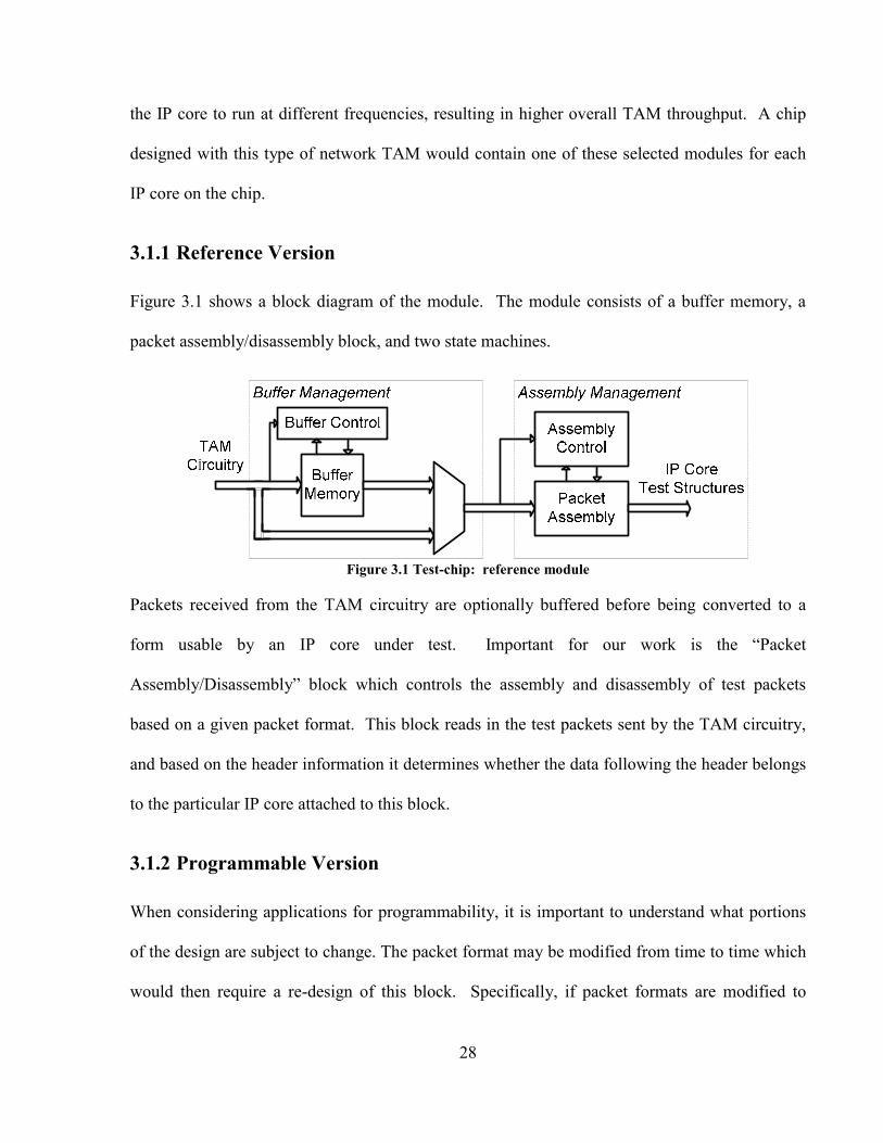
Figure 3.1 shows a block diagram of the module. The module consists of a buffer memory, a
packet assembly/disassembly block, and two state machines.
Figure 3.1 Test-chip: reference module
Packets received from the TAM circuitry are optionally buffered before being converted to a
form usable by an IP core under test. Important for our work is the “Packet
Assembly/Disassembly” block which controls the assembly and disassembly of test packets
based on a given packet format. This block reads in the test packets sent by the TAM circuitry,
and based on the header information it determines whether the data following the header belongs
to the particular IP core attached to this block.
3.1.2 Programmable Version
When considering applications for programmability, it is important to understand what portions
of the design are subject to change. The packet format may be modified from time to time which
would then require a re-design of this block. Specifically, if packet formats are modified to
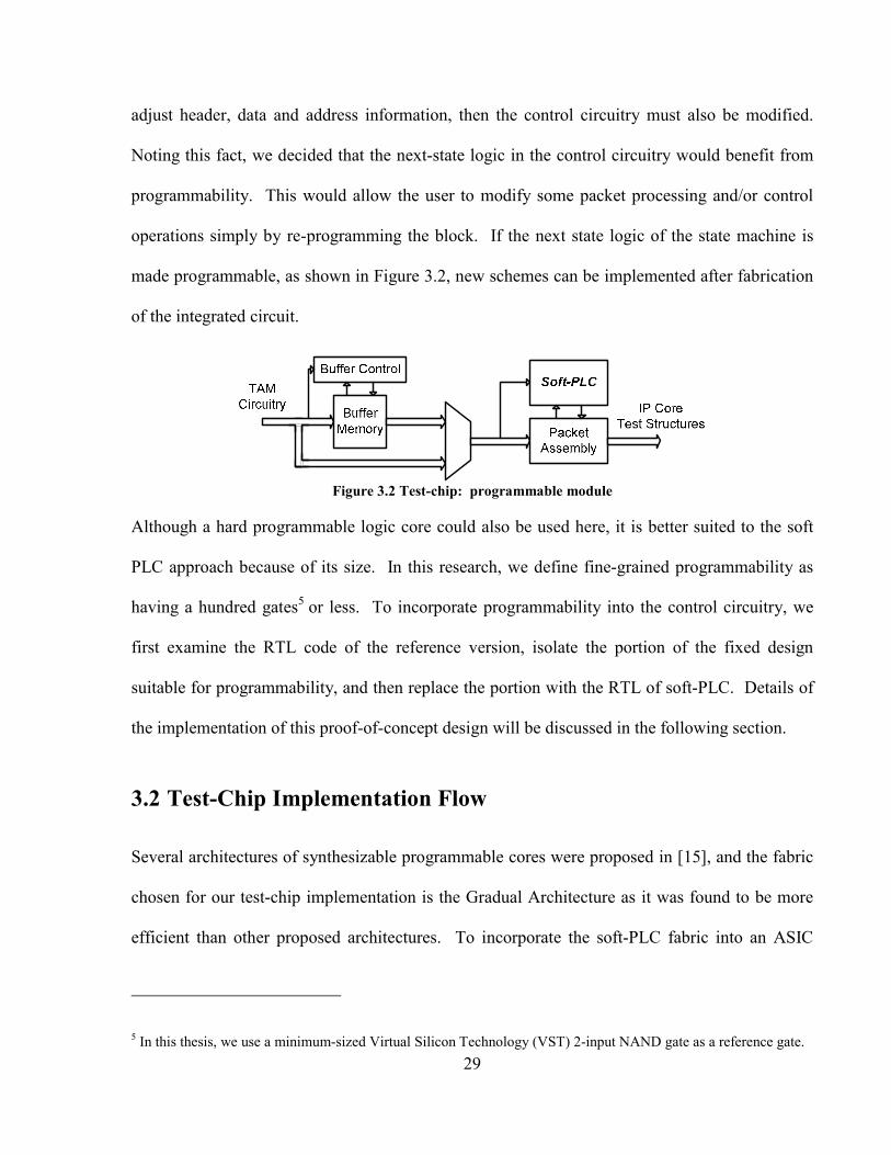
29
adjust header, data and address information, then the control circuitry must also be modified.
Noting this fact, we decided that the next-state logic in the control circuitry would benefit from
programmability. This would allow the user to modify some packet processing and/or control
operations simply by re-programming the block. If the next state logic of the state machine is
made programmable, as shown in Figure 3.2, new schemes can be implemented after fabrication
of the integrated circuit.
Figure 3.2 Test-chip: programmable module
Although a hard programmable logic core could also be used here, it is better suited to the soft
PLC approach because of its size. In this research, we define fine-grained programmability as
having a hundred gates5 or less. To incorporate programmability into the control circuitry, we
first examine the RTL code of the reference version, isolate the portion of the fixed design
suitable for programmability, and then replace the portion with the RTL of soft-PLC. Details of
the implementation of this proof-of-concept design will be discussed in the following section.
3.2 Test-Chip Implementation Flow
Several architectures of synthesizable programmable cores were proposed in [15], and the fabric
chosen for our test-chip implementation is the Gradual Architecture as it was found to be more
efficient than other proposed architectures. To incorporate the soft-PLC fabric into an ASIC
5 In this thesis, we use a minimum-sized Virtual Silicon Technology (VST) 2-input NAND gate as a reference gate.
30
design, additional steps are introduced to the typical IC design flow. The modified IC design
flow is the main focus of the following subsections.
3.2.1 Modified ASIC IC Design Flow
Referring to Section 1.1, the main advantage of using a soft-PLC is its ease-of-use with the
existing ASIC design flow. Keeping this requirement in mind, all modifications to the existing
ASIC design were kept to a minimum, and the proposed new flow is depicted in Figure 3.3. The
additional steps introduced to the existing ASIC IC design flow are high-lighted in gray.
Figure 3.3 Modified IC implementation flow
The soft-PLC RTL is automatically generated by a Tcl script [15]. A user-defined circuit is first
written in VHDL, and then converted to Berkeley’s BLIF format through a series of utilities
[40][41]. The circuit then goes through technology-independent optimization, followed by
technology-mapping to 3-LUT logic blocks [42][43]. The technology-mapped circuit is then
packed [44], and placed and routed using VPR. Based on the routed circuit, the configuration
bits are generated; these bits are used to program the soft-PLC for simulation and testing.
31
The integration of soft-PLC RTL into the ASIC design was found to be quite straight-forward.
Since the soft-PLC fabric is written in VHDL, it can be instantiated as if it were a regular ASIC
module. Once the integration is completed, the programmable design is ready for synthesis.
3.2.2 Front-end IC Design Flow
Front-end IC design flow encompasses synthesis and functional verification of the design.
Design Compiler from Synopsys was used to synthesize the programmable design into a
technology-dependent, gate-level netlist. The technology used for synthesis is the 0.18 µm
Virtual Silicon Technology [47] standard cell libraries. A mixed compile strategy was used,
where a top-down compilation on each module (soft-PLC fabric, Packet Assembly, Buffer
Memory, and Buffer Control) was followed by a bottom-up compilation to tie each module into a
complete design [45]. To achieve improved synthesis results, levels of hierarchy in the design
were removed, so that Design Compiler could perform cross-boundary optimization.
Before continuing on with the physical design part of the IC design flow, the synthesized circuit
needs to be functionally verified. Functional verification of a circuit is the process of ensuring
that the logical design of the circuit satisfies the architectural specification. Standard techniques
in function verification include hardware modeling and simulation, random and focused stimulus
generation and coverage analysis [46]. Here, we are particularly concerned with the correct
behavior of the hardware; this is done through functional simulation. Simulations are performed
before and after the synthesis to ensure that the logical and timing characteristics of the design
still meets the specification after synthesis.
32
Although functional verification is a well-understood process in the IC design flow, it is
worthwhile mentioning the impact of soft-PLC on this process. By nature, an embedded
programmable logic core does not perform any specific functions until it is configured.
Simulating an un-programmed soft-PLC does not yield meaningful information; hence, we need
to include the programming of the soft-PLC fabric as part of the simulation. This is a key point
to emphasize in the verification of programmable logic: first program the bits and then carry out
functional simulation. Figure 3.4 illustrates the functional simulation process.
Figure 3.4 Function simulation: (a) configuration phase (b) normal phase
In Figure 3.4(a), upon the start of simulation, only the configuration shift_in and config_clk ports
are active. Through this process, the configuration bits are stored in the D flip-flops; all flip-
flops are daisy-chained together, allowing the configuration bits to be serially shifted into the
fabric. On the rising edge of each configuration clock cycle, exactly one configuration bit is
shifted into the fabric; the config_clk is deactivated as soon as the last configuration bit is loaded.
During the configuration period, data input ports and sys_clk are turned off, and the output ports
are not probed. Once the programming is done, the data input ports and sys_clk start to toggle,
and data outputs can be probed. A set of stimulus is supplied to the input ports and sampled on
the falling edge of the sys_clk. The output ports are then probed and compared to a set of
33
expected outputs to verify the correct behavior of the design. Once the design is verified in this
manner, it is ready for the physical portion of the IC design flow.
3.2.3 Back-end IC Design Flow
As described in Section 2.1.2, the back-end, or the physical portion, of the IC design flow
includes floorplanning, placement, clock-tree synthesis, routing, design-rule-checking (DRC),
layout-vs.-schematic (LVS) checking, and timing verification. The Physical Design Planner
(PDP) tool from Cadence was used for floorplanning, placement and clock-tree synthesis. For
routing, the Cadence tool Silicon Ensemble (SE) was used; LVS was performed in Cadence
Virtuoso; and timing verification was performed in Verilog-XL.
One observation at this stage of the implementation is the choice of the core utilization factor
during floorplanning– a number expressed as a percentage, or in decimal form, that indicates
how much of the total core area is dedicated to the standard cells. For example, a core utilization
of 0.75 means that 75% of the core area is used for circuit blocks and 25% of the core area is
reserved for power striping, power routing, clock-tree synthesis, and standard cell routing. A
typical value of 0.75 was suggested in the CMC IC design flow tutorial [18].
However, it was found after placement and routing that a value of 0.75 was too large for our
programmable design: the routing in SE failed due to numerous geometry violations. Since our
programmable design was I/O pad limited – meaning more core area than is required is available
– the core utilization factor could be relaxed. It was found by trial and error that a core
utilization of 0.55 resulted in better placement and routing quality. Choosing a suitable core
utilization factor is an iterative process. Nonetheless, a trend was observed with regard to the
34
core utilization factor chosen: a higher factor generally means more constrained placement and
routing and longer run times, but a lower factor may have other unwanted side-effects, such as
longer delays and antenna violations, due to longer metal interconnect. At a core utilization of
0.55, no antenna violations were detected by DRC in SE.
After placement and routing, LVS was performed in Virtuoso to ensure that the layout matches
functionally with the gate-level schematics. Occasionally, unintended connections may be made
during the placement and routing, and this type of error would be flagged during LVS. No LVS
errors were found in the programmable design and after passing DRC checks offered by CMC
[18], the programmable version of our proof-of-concept design was signed off for fabrication.
3.3 Design and Implementation Issues
When adding a programmable component to an ASIC module, several design and
implementation issues arose: programmable core size selection, I/O connections, and clock-tree
synthesis. This section describes these issues and how they were resolved.
3.3.1 Programmable Core Size Selection
The first issue was how much programmable logic is needed to replace the fixed next state logic.
Without knowing the actual logic function that will eventually be implemented in the core, it is
difficult to estimate the amount of programmable logic required. Too large a programmable core
would result in wasted silicon and a slower circuit, but too little would render the core unusable.
In this case, we have knowledge regarding the types of functions that will be implemented (we
call his domain knowledge), and we can use this knowledge to make reasonable decisions. We
designed two user-defined logic functions that could be implemented in the programmable core;
35
these two logic functions are two distinct next state machines. We then determined the size of
the core that would be required to implement each function. For our circuits, we found that a
core consisting of 49 LUTs (i.e., a 7 x 7 array of 3-LUTs) would be sufficient for both potential
logic functions; however, to allow some safety margin and to anticipate larger functions, a core
of 64 LUTs (an 8 x 8 array) was used. Based on the observations made from working with core
size selection, typically one extra row and column should be added to allow for future
developments, although the actual increase should be based on the specific application.
3.3.2 Connections between Programmable Core and Fixed Logic
A second issue is how the programmable logic core is connected to the rest of the ASIC module.
Although the core itself is programmable, specific inputs and outputs must be connected to the
core in advance. This will dictate, and perhaps limit, the possible functions that can be
implemented in the core. This issue is common to all types of embedded programmable logic,
and the connections cannot be easily altered after the chip is fabricated. Fortunately, we have
domain knowledge to assist us with the I/O connection decision. We can select which inputs are
connected to the core and which outputs will be made available from the core. In our design, the
two user logic functions required 9 inputs and 10 inputs respectively, and required 11 outputs
and 12 outputs respectively. Some flexibility was possible by hardwiring a selected set of 10
inputs and 13 outputs to our core.
Determining the right connections requires careful planning and often relies on the designer’s
experience. Take a programmable state machine for example: the total number of states is
dictated by the number of bits available to represent the states in binary digits, as illustrated in
Figure 3.5.
36
Figure 3.5 State machine in soft-PLC: (a) 8 states, (b) 16 states.
In our reference design, the original state machine would require only 3 inputs to represent the
seven known states. To allow more flexibility in our logic functions, we used 4 inputs, which
would give us 16 states. Of course, any logic that may be affected by a change in state must be
handled within the programmable core as well.
3.3.3 Routing the Programmable Clock Signals
During the physical design process, it became apparent that our synthesizable core was placing
an extra burden on the clock routing due to the large number of flip-flops (FF) in the design. A
programmable logic core contains many configuration bits to store the state of individual routing
switches and the contents of lookup-tables; in a synthesizable core, these configuration bits are
built using flip-flops that have clock inputs to enable programming.
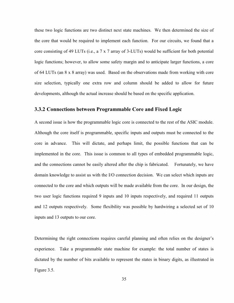
As shown in Figure 3.6(a), there are configuration bits for input muxes and output muxes, as
well as the LUTs themselves. Each of these FF’s must be connected to a common clock signal
for the programming purpose; the clock net is highlight in Figure 3.6(b). Clearly, the over use of
FF’s has produced a clock net that is forced to wind its way around the core in a circuitous
fashion. This is not typically the case in a regular ASIC block.
37
(a) Portion of Gradual Architecture
FF
FF
FF
FF
FF
FF
FF
FF
LUT block
FF FF FF
FF FF FF
FF
FF
FF
FF
FF
FF
FF
FF
LUT block
FF FF FF
FF FF FF
Bit Config Clock
Input Muxes
Routing Muxes
(b) Physical Design of Programmable Module Figure 3.6 Programmable clock tree routing complexity
To determine how flip-flop-intensive our core is, we compared its flip-flop density to that of a
non-programmable design. We analyzed an ASIC implementation of a 68HC11 core, and found
that the flip-flop density (number of flip-flops per unit area) was 1/3 of the flip-flop density in
our programmable logic core. With the number of flip flops in our programmable design, we
realized that the clock tree in our core will be more complex and consume more chip area than a
typical ASIC. This was confirmed; in our implementation, 45% of the layout area was reserved
for the clock tree, power striping, and signal routing. Furthermore, FF’s must be connected as
one long shift register for programming purposes, and this also added to the routing complexity.
Closer examination of the programmable core revealed one problem: some extra buffers were
inserted in between the FF’s. The ratio of the FF’s to the extra buffers was about 2:1. These
buffers were inserted by the synthesis tool to satisfy the hold time requirement [49]:
qclkholdskewdmin TTTT −−+>
38
where Tdmin is the delay through the combinational logic, Tskew is the clock skew, Thold is the hold
time and Tclk-q is the delay in the FF from the clock input to the output, Q. While Thold and Tclk-q
are defined by the standard cell library, Tskew and Tdmin can only be determined after the
placement and routing. However, the synthesis tool requires an estimated Tskew value specified
by the designer in order to check for and fix any setup and hold time violations. In our synthesis
script, Tskew for config_clk was set at 0.4ns; this value was found to be significantly larger than
necessary. Since consecutive FF’s are close to each other, the clock skew variations were small.
In fact, the worst clock skew observed after placement and routing were only 70ps (0.07ns). By
re-synthesizing the programmable core with Tskew of 0.10ns, the extra buffers were eliminated;
the area of the synthesized programmable core was reduced by 3.5%. The synthesized area of
the programmable core is reported in Table 3.1 in Section 3.4.1.
3.4 Implementation Results
In this section, we present a comparison between the reference and the programmable designs in
terms of area and speed, obtained from both synthesis and physical layout.
3.4.1 Area Overhead
After the synthesis stage, the reference module (without the programmable logic core) required
234 536 µm2 in a 0.18µm TSMC process, of which 590 µm2 is the area due to the assembly
controller next state logic. The programmable module (containing 64 LUTs as described in
Section 3.3.1) required 612 873 µm2, of which 321 545 µm2 was due to the programmable next
state logic. The synthesized areas as well as the gate counts are summarized in Table 3.1. The
39
gate count estimates were obtained by normalizing the area of the design to that of a basic 2-
input NAND gate (size = 11.53 µm2) [47].
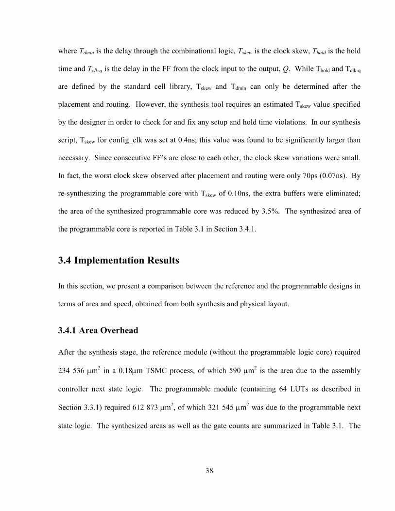
Table 3.1 Post-Synthesis Area and Gate Count Summery
Implementation Method
Area of Next State Logic
Gate Count of Next State Logic
Area of Entire Design
Gate Count of Entire Design
Reference Version 590 µm2 51 234 536 µm2 20 341 Programmable Version (Tskew=0.4ns) 321 545 µm2 27 880 612 873 µm2 53 155
Programmable Version (Tskew=0.1ns) 310 295 µm2 26 912 601 253 µm2 52 147
After the physical design stage, the reference module (without the programmable logic core)
required 369 700 µm2 of silicon space, of which 1 217 µm2 is the area due to the assembly
controller next state logic. The programmable required 1 025 000 µm2, of which 684 600 µm2
was due to the programmable next state logic.
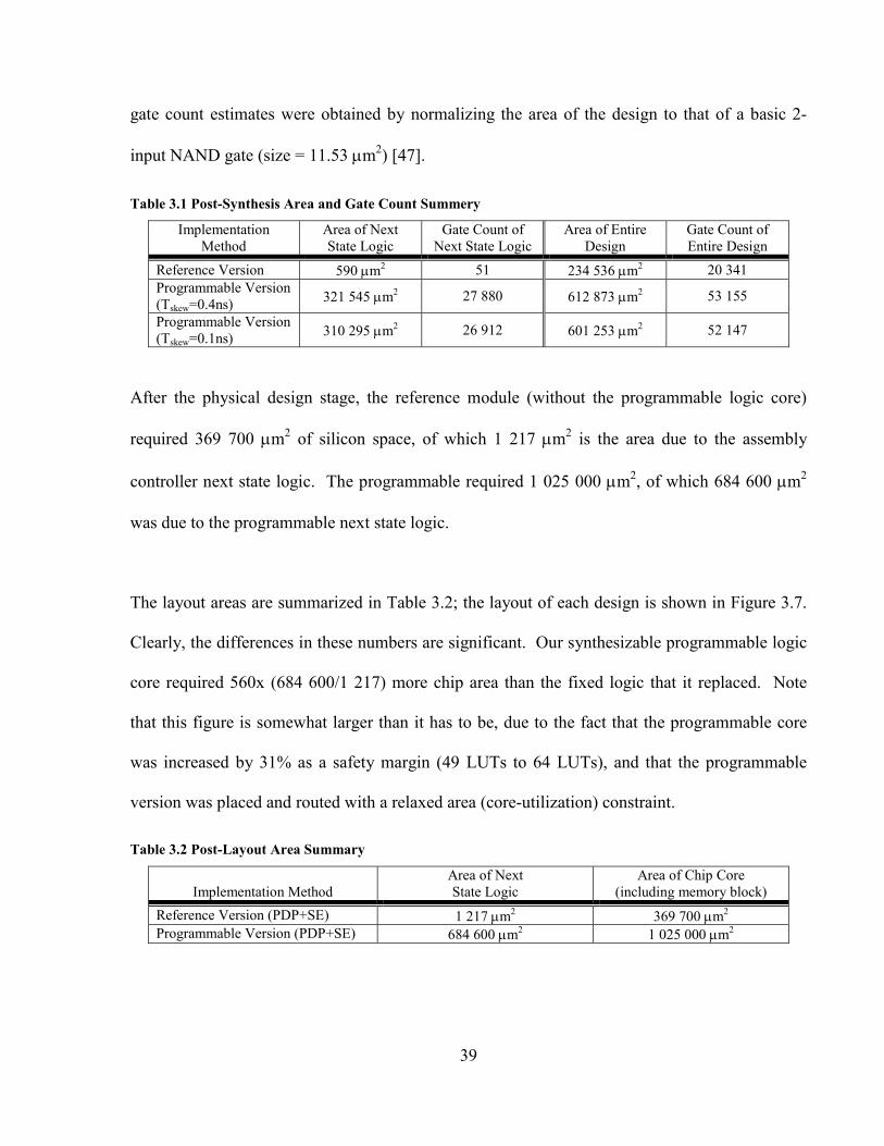
The layout areas are summarized in Table 3.2; the layout of each design is shown in Figure 3.7.
Clearly, the differences in these numbers are significant. Our synthesizable programmable logic
core required 560x (684 600/1 217) more chip area than the fixed logic that it replaced. Note
that this figure is somewhat larger than it has to be, due to the fact that the programmable core
was increased by 31% as a safety margin (49 LUTs to 64 LUTs), and that the programmable
version was placed and routed with a relaxed area (core-utilization) constraint.
Table 3.2 Post-Layout Area Summary
Implementation Method
Area of Next State Logic
Area of Chip Core (including memory block)
Reference Version (PDP+SE) 1 217 µm2 369 700 µm2 Programmable Version (PDP+SE) 684 600 µm2 1 025 000 µm2
40
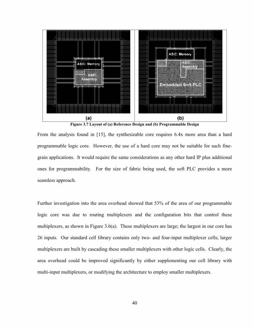
Figure 3.7 Layout of (a) Reference Design and (b) Programmable Design
From the analysis found in [15], the synthesizable core requires 6.4x more area than a hard
programmable logic core. However, the use of a hard core may not be suitable for such fine-
grain applications. It would require the same considerations as any other hard IP plus additional
ones for programmability. For the size of fabric being used, the soft PLC provides a more
seamless approach.
Further investigation into the area overhead showed that 53% of the area of our programmable
logic core was due to routing multiplexers and the configuration bits that control these
multiplexers, as shown in Figure 3.6(a). These multiplexers are large; the largest in our core has
26 inputs. Our standard cell library contains only two- and four-input multiplexer cells; larger
multiplexers are built by cascading these smaller multiplexers with other logic cells. Clearly, the
area overhead could be improved significantly by either supplementing our cell library with
multi-input multiplexers, or modifying the architecture to employ smaller multiplexers.
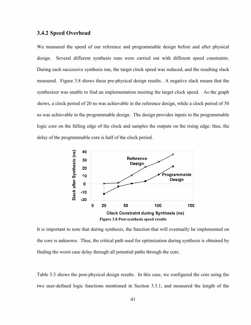
41
3.4.2 Speed Overhead
We measured the speed of our reference and programmable design before and after physical
design. Several different synthesis runs were carried out with different speed constraints.
During each successive synthesis run, the target clock speed was reduced, and the resulting slack
measured. Figure 3.8 shows these pre-physical design results. A negative slack means that the
synthesizer was unable to find an implementation meeting the target clock speed. As the graph
shows, a clock period of 20 ns was achievable in the reference design, while a clock period of 50
ns was achievable in the programmable design. The design provides inputs to the programmable
logic core on the falling edge of the clock and samples the outputs on the rising edge; thus, the
delay of the programmable core is half of the clock period.
Figure 3.8 Post-synthesis speed results
It is important to note that during synthesis, the function that will eventually be implemented on
the core is unknown. Thus, the critical path used for optimization during synthesis is obtained by
finding the worst case delay through all potential paths through the core.
Table 3.3 shows the post-physical design results. In this case, we configured the core using the
two user-defined logic functions mentioned in Section 3.3.1, and measured the length of the
g
42
critical path through the logic circuit in each case. As the table shows, the results indicate that
the programmable design has approximately twice the critical path delay as the reference design,
for both user-defined functions.
Table 3.3 Post-Layout Speed Results
Implementation Method Critical Path of IC (using first logic function)
Critical Path of IC (using second logic function)
Reference Module (no programmability) 25.40 ns 25.40 ns
Programmable Module (with synthesizable core) 51.08 ns 51.08 ns
It is important to note that the critical path delays shown here are the critical path delays of the
entire design, not just through the programmable core itself. A detailed delay study on
programmable core considered separately is discussed in Chapter 4.
3.4.3 Validation of Chip on Tester
The test chip was validated on the Agilent 81200 data generator/analyzer platform. The
measured critical path delay for each user-defined logic function is summarized in Table 3.4.
The chip design had a critical path delay of about 40ns. Compared to the 50ns obtained from the
simulations, this value is within the statistical variations of the CMOS process6.
Table 3.4 Speed Measurements: Simulation Speed vs. Measured Speed
Speed Measurements Critical Path of IC (using first logic function)
Critical Path of IC (using second logic function)
Simulation Speed 51.08 ns 51.08 ns Measured Speed on Tester 40.60 ns 40.40 ns
6 SPICE simulations of a minimum sized buffer (in TSMC 0.18um technology) subject to different PVT (process, voltage, temperature) corners showed a speed variation up to 26ps relative to the typical case. This translates to about 30% variation. Generally accepted speed variation due to PVT is 20% to 40%.
43
Average on-chip power measurements were also obtained and summarized in Table 3.5. The test
chip was configured once, and the input vectors were looped indefinitely, while the current was
measured from the test chip. The core current is drawn by the power grid that covers the core of
the chip, and is drawn from a 1.8V DC source. The I/O current is drawn by the power ring that
feeds the I/O pads around the chip periphery, and is drawn from a 3.3V DC source. The average
power is simply computed by the equation DDmeasuredaverage VIP ⋅= . For the core power dissipation,
the dynamic power equation clkdynamic fVCP ⋅⋅⋅= 2α , which constitutes about 90% of the total
power dissipation in 0.18µm technology, holds true as the clock frequency changes.
Table 3.5 Off-chip Power Measurements
User-defined Logic Function Power Type CLK = 16.7 Mhz CLK = 33 Mhz CLK = 62.5 Mhz
Core (mW) 3.65 7.16 13.14 First Logic Function I/O (mW) 129.56 130.85 131.97
Core (mW) 4.27 8.35 12.44 Second Logic Function I/O (mW) 122.30 123.78 124.97
Unfortunately, the reference ASIC design was not fabricated, due to silicon space limitation, and
therefore, we could not compare the power dissipation of both designs. However, a power
estimate of the programmable core could still be obtained through power simulation tools, and a
detailed power study can be found in Chapter 4.
3.5 Summary
In this chapter, the implementation of a proof-of-concept programmable module using the soft
core approach has been described. Several implementation issues have been discussed: the
choice of the size of a core, the choice of inputs and outputs, and the difficulty in routing the
clock signal to the flip-flips. Domain knowledge of user circuits to be implemented on a
44
programmable core is essential in determining the size of the core required. Similarly, domain
knowledge can also assist us with the I/O connections. Proper timing constraint helps to
minimize the complexity of the configuration clock network; however, the majority of the clock
complexity is due to the large number of flip-flops required to store the configuration bits.
Two versions of the test-chip were designed: the baseline design architecture, and the
programmable version containing a piece of “soft core” programmable fabric. Only the
programmable version was fabricated, and it has been tested on an Agilent 81200 analyzer. We
have successfully validated the concept of synthesizable programmable logic cores through
physical implementation on silicon. Measurements off the chip suggested that we should focus
on the speed and power, which is the main topic of the next chapter.
45
Chapter 4
Speed and Power Considerations for Soft-PLC
Although soft embedded programmable logic cores provide the convenience of flexibility and
lower NRE cost, the associated overhead in area, speed and power dissipation are significant
when compared with ASIC designs. While silicon area is becoming relatively cheap due to
technology scaling, speed and power remain as major challenges for FPGA designers. In this
chapter, we first describe experimental methodologies employed to quantify the area, and speed
overhead associated with the Gradual Architecture synthesizable programmable logic core. We
then explore a speed optimization technique using the existing CAD tools, followed by the
experimental results to evaluate the effectiveness of this approach. Finally, we quantify the
power overhead associated with the Gradual Architecture and present some future research
directions for the power issues.
4.1 Speed Considerations
There are two distinct types of delays in a programmable logic core: worst-case feasible delay
and worst-case functional delay. This section describes how these two types of delays are
different and how they are measured. Then it presents the delay overhead of using a soft-PLC
when compared to the equivalent ASIC implementation. Finally, it describes a technique to
reduce the critical-path delays based on additional CAD tool effort.
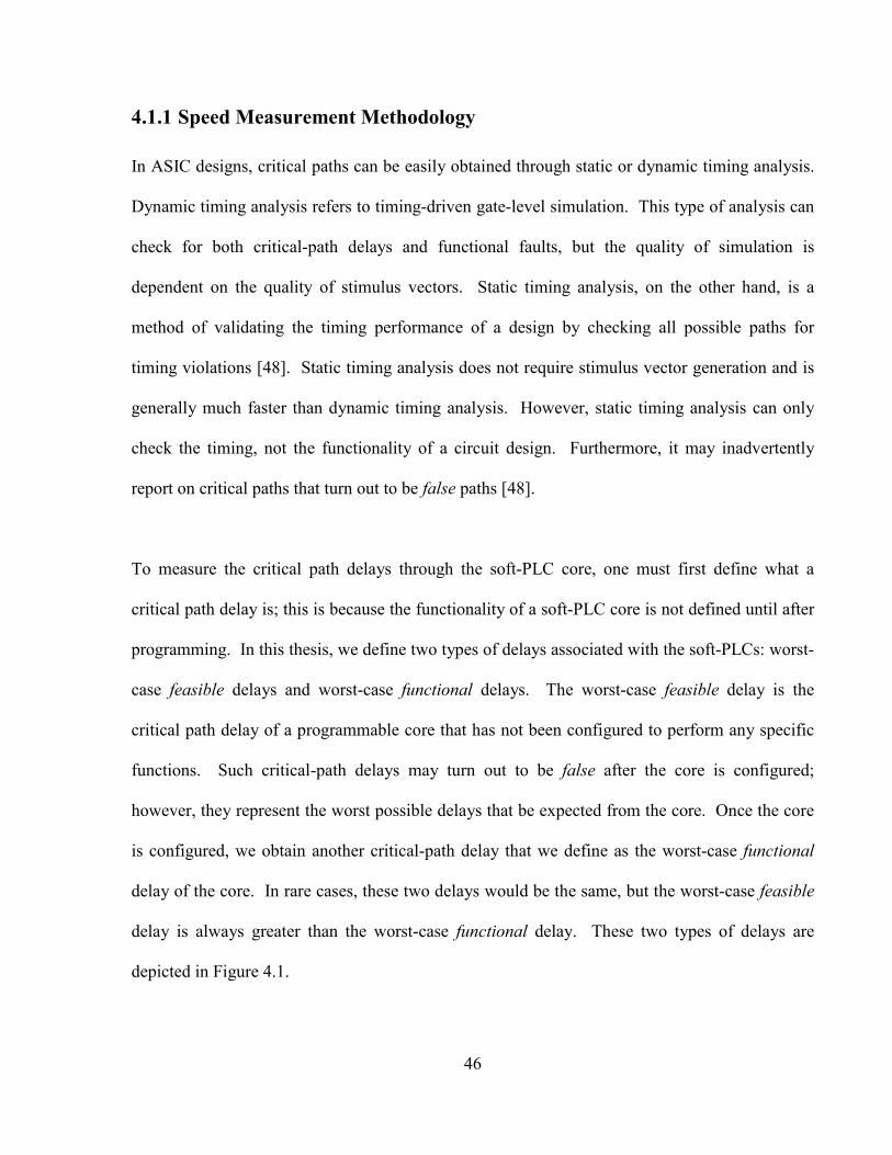
46
4.1.1 Speed Measurement Methodology
In ASIC designs, critical paths can be easily obtained through static or dynamic timing analysis.
Dynamic timing analysis refers to timing-driven gate-level simulation. This type of analysis can
check for both critical-path delays and functional faults, but the quality of simulation is
dependent on the quality of stimulus vectors. Static timing analysis, on the other hand, is a
method of validating the timing performance of a design by checking all possible paths for
timing violations [48]. Static timing analysis does not require stimulus vector generation and is
generally much faster than dynamic timing analysis. However, static timing analysis can only
check the timing, not the functionality of a circuit design. Furthermore, it may inadvertently
report on critical paths that turn out to be false paths [48].
To measure the critical path delays through the soft-PLC core, one must first define what a
critical path delay is; this is because the functionality of a soft-PLC core is not defined until after
programming. In this thesis, we define two types of delays associated with the soft-PLCs: worst-
case feasible delays and worst-case functional delays. The worst-case feasible delay is the
critical path delay of a programmable core that has not been configured to perform any specific
functions. Such critical-path delays may turn out to be false after the core is configured;
however, they represent the worst possible delays that be expected from the core. Once the core
is configured, we obtain another critical-path delay that we define as the worst-case functional
delay of the core. In rare cases, these two delays would be the same, but the worst-case feasible
delay is always greater than the worst-case functional delay. These two types of delays are
depicted in Figure 4.1.
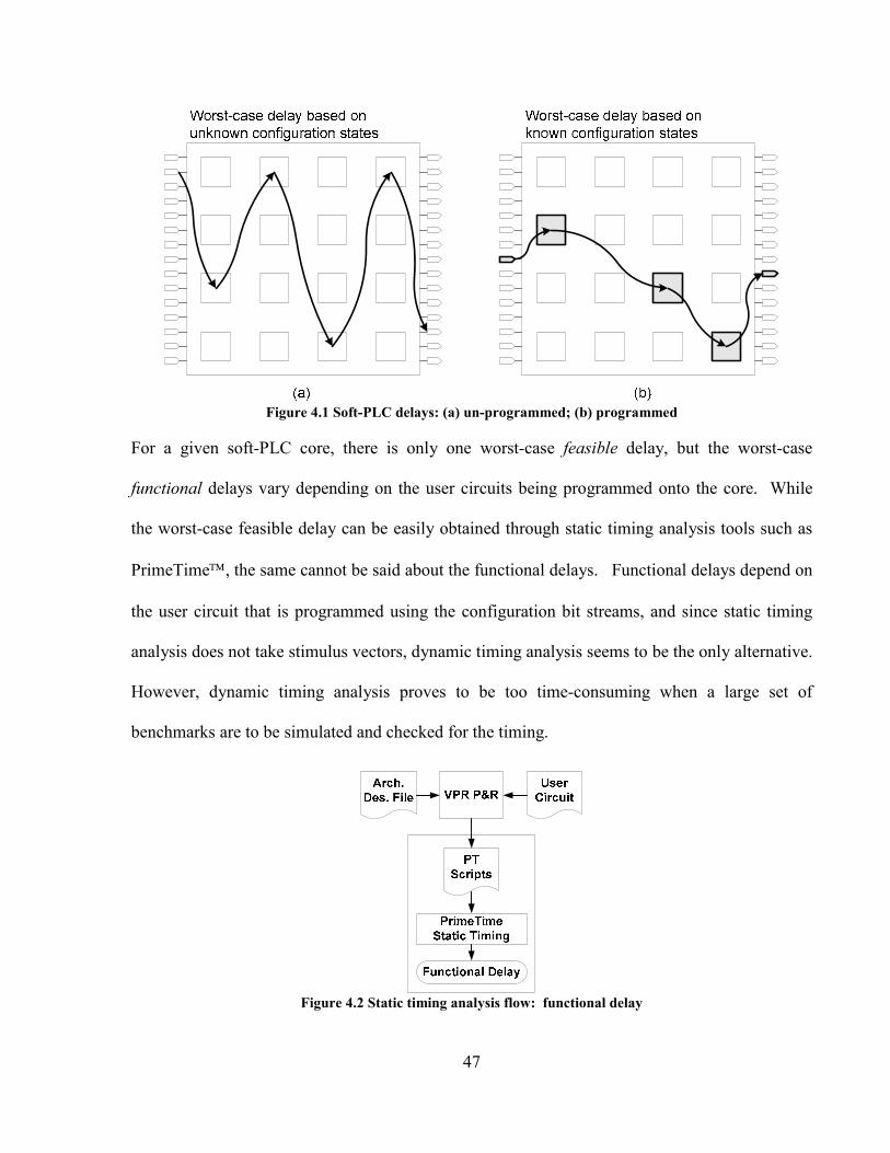
47
Figure 4.1 Soft-PLC delays: (a) un-programmed; (b) programmed
For a given soft-PLC core, there is only one worst-case feasible delay, but the worst-case
functional delays vary depending on the user circuits being programmed onto the core. While
the worst-case feasible delay can be easily obtained through static timing analysis tools such as
PrimeTime, the same cannot be said about the functional delays. Functional delays depend on
the user circuit that is programmed using the configuration bit streams, and since static timing
analysis does not take stimulus vectors, dynamic timing analysis seems to be the only alternative.
However, dynamic timing analysis proves to be too time-consuming when a large set of
benchmarks are to be simulated and checked for the timing.
Figure 4.2 Static timing analysis flow: functional delay
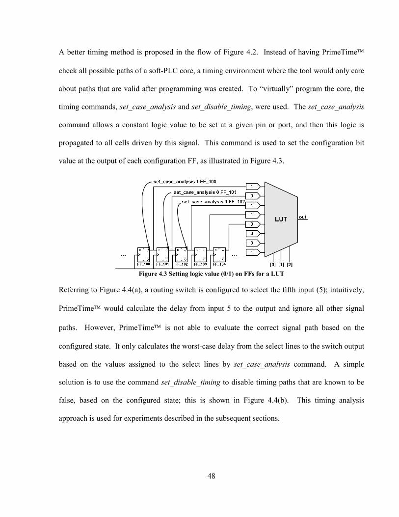
48
A better timing method is proposed in the flow of Figure 4.2. Instead of having PrimeTime
check all possible paths of a soft-PLC core, a timing environment where the tool would only care
about paths that are valid after programming was created. To “virtually” program the core, the
timing commands, set_case_analysis and set_disable_timing, were used. The set_case_analysis
command allows a constant logic value to be set at a given pin or port, and then this logic is
propagated to all cells driven by this signal. This command is used to set the configuration bit
value at the output of each configuration FF, as illustrated in Figure 4.3.
Figure 4.3 Setting logic value (0/1) on FFs for a LUT
Referring to Figure 4.4(a), a routing switch is configured to select the fifth input (5); intuitively,
PrimeTime would calculate the delay from input 5 to the output and ignore all other signal
paths. However, PrimeTime is not able to evaluate the correct signal path based on the
configured state. It only calculates the worst-case delay from the select lines to the switch output
based on the values assigned to the select lines by set_case_analysis command. A simple
solution is to use the command set_disable_timing to disable timing paths that are known to be
false, based on the configured state; this is shown in Figure 4.4(b). This timing analysis
approach is used for experiments described in the subsequent sections.
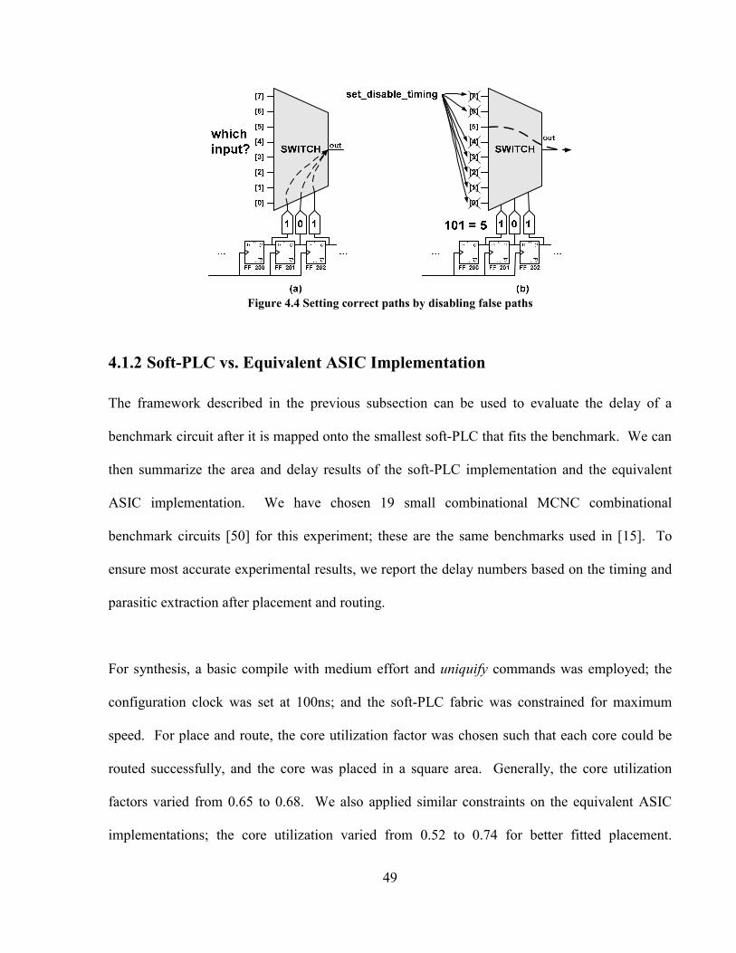
49
Figure 4.4 Setting correct paths by disabling false paths
4.1.2 Soft-PLC vs. Equivalent ASIC Implementation
The framework described in the previous subsection can be used to evaluate the delay of a
benchmark circuit after it is mapped onto the smallest soft-PLC that fits the benchmark. We can
then summarize the area and delay results of the soft-PLC implementation and the equivalent
ASIC implementation. We have chosen 19 small combinational MCNC combinational
benchmark circuits [50] for this experiment; these are the same benchmarks used in [15]. To
ensure most accurate experimental results, we report the delay numbers based on the timing and
parasitic extraction after placement and routing.
For synthesis, a basic compile with medium effort and uniquify commands was employed; the
configuration clock was set at 100ns; and the soft-PLC fabric was constrained for maximum
speed. For place and route, the core utilization factor was chosen such that each core could be
routed successfully, and the core was placed in a square area. Generally, the core utilization
factors varied from 0.65 to 0.68. We also applied similar constraints on the equivalent ASIC
implementations; the core utilization varied from 0.52 to 0.74 for better fitted placement.
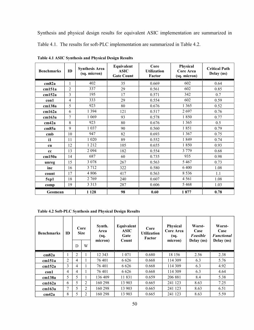
50
Synthesis and physical design results for equivalent ASIC implementation are summarized in
Table 4.1. The results for soft-PLC implementation are summarized in Table 4.2.
Table 4.1 ASIC Synthesis and Physical Design Results
Benchmarks ID Synthesis Area (sq. micron)
Equivalent ASIC
Gate Count
Core Utilization
Factor
Physical Core Area
(sq. micron)
Critical Path Delay (ns)
cm82a 1 402 35 0.669 602 0.64 cm151a 2 337 29 0.561 602 0.85 cm152a 3 195 17 0.571 342 0.7
con1 4 333 29 0.554 602 0.59 cm138a 5 923 80 0.676 1 365 0.52 cm162a 6 1 394 121 0.517 2 697 0.76 cm163a 7 1 069 93 0.578 1 850 0.77 cm42a 8 923 80 0.676 1 365 0.5 cm85a 9 1 037 90 0.560 1 851 0.79 cmb 10 947 82 0.693 1 367 0.75
i1 11 1 020 89 0.552 1 849 0.74 cu 12 1 212 105 0.655 1 850 0.93 cc 13 2 094 182 0.554 3 779 0.68
cm150a 14 687 60 0.735 935 0.98 unreg 15 3 078 267 0.563 5 467 0.73
inc 16 3 712 322 0.580 6 400 1.08 count 17 4 806 417 0.563 8 536 1.1 5xp1 18 2 769 240 0.607 4 561 1.08 comp 19 3 313 287 0.606 5 468 1.03
Geomean 1 128 98 0.60 1 877 0.78
Table 4.2 Soft-PLC Synthesis and Physical Design Results
Core Size Benchmarks ID
D W
Synth. Area (sq.
micron)
Equivalent ASIC Gate
Count
Core Utilization
Factor
Physical Core Area
(sq. micron)
Worst-Case
Feasible Delay (ns)
Worst-Case
Functional Delay (ns)
cm82a 1 2 1 12 343 1 071 0.680 18 156 2.56 2.38 cm151a 2 4 1 76 401 6 626 0.668 114 309 6.3 5.76 cm152a 3 4 1 76 401 6 626 0.668 114 309 6.3 4.92
con1 4 4 1 76 401 6 626 0.668 114 309 6.3 4.64 cm138a 5 5 1 136 409 11 831 0.659 206 881 8.4 5.38 cm162a 6 5 2 160 298 13 903 0.665 241 123 8.63 7.25 cm163a 7 5 2 160 298 13 903 0.665 241 123 8.63 6.51 cm42a 8 5 2 160 298 13 903 0.665 241 123 8.63 5.59
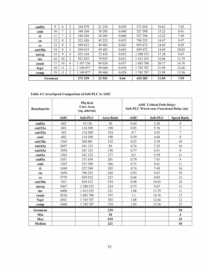
51
cm85a 9 6 2 244 879 21 238 0.659 371 654 10.62 7.43 cmb 10 7 2 348 268 30 205 0.660 527 398 13.22 8.41
i1 11 7 2 348 268 30 205 0.660 527 398 13.22 7.49 cu 12 8 2 521 426 45 223 0.655 796 252 14.67 9.47 cc 13 8 3 569 615 49 403 0.663 859 472 14.69 8.05
cm150a 14 8 3 569 615 49 403 0.663 859 472 14.69 10.03 unreg 15 9 4 835 164 72 434 0.652 1 280 533 17.38 9.67
inc 16 10 2 921 855 79 953 0.651 1 415 255 19.46 11.79 count 17 10 4 1 107 156 96 024 0.657 1 685 708 20.17 14.76 5xp1 18 11 2 1 149 077 99 660 0.658 1 745 787 21.98 12.66 comp 19 11 2 1 149 077 99 660 0.658 1 745 787 21.98 15.56
Geomean 271 539 23 551 0.66 410 285 11.05 7.59
Table 4.3 Area/Speed Comparison of Soft-PLC to ASIC
Physical Core Area
(sq. micron)
ASIC Critical Path Delay/ Soft-PLC Worst-case Functional Delay (ns) Benchmarks
ASIC Soft-PLC Area Ratio ASIC Soft-PLC Speed Ratio
cm82a 602 18 156 30 0.64 2.38 4 cm151a 602 114 309 190 0.85 5.76 7 cm152a 342 114 309 334 0.7 4.92 7
con1 602 114 309 190 0.59 4.64 8 cm138a 1365 206 881 152 0.52 5.38 10 cm162a 2697 241 123 89 0.76 7.25 10 cm163a 1850 241 123 130 0.77 6.51 8 cm42a 1365 241 123 177 0.5 5.59 11 cm85a 1851 371 654 201 0.79 7.43 9 cmb 1367 527 398 386 0.75 8.41 11
i1 1849 527 398 285 0.74 7.49 10 cu 1850 796 252 430 0.93 9.47 10 cc 3779 859 472 227 0.68 8.05 12
cm150a 935 859 472 919 0.98 10.03 10 unreg 5467 1 280 533 234 0.73 9.67 13
inc 6400 1 415 255 221 1.08 11.79 11 count 8536 1 685 708 197 1.1 14.76 13 5xp1 4561 1 745 787 383 1.08 12.66 12 comp 5468 1 745 787 319 1.03 15.56 15
Geomean 219 10 Min 30 4 Max 919 15
Median 221 10
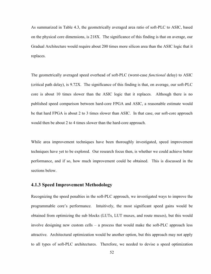
52
As summarized in Table 4.3, the geometrically averaged area ratio of soft-PLC to ASIC, based
on the physical core dimensions, is 218X. The significance of this finding is that on average, our
Gradual Architecture would require about 200 times more silicon area than the ASIC logic that it
replaces.
The geometrically averaged speed overhead of soft-PLC (worst-case functional delay) to ASIC
(critical path delay), is 9.72X. The significance of this finding is that, on average, our soft-PLC
core is about 10 times slower than the ASIC logic that it replaces. Although there is no
published speed comparison between hard-core FPGA and ASIC, a reasonable estimate would
be that hard FPGA is about 2 to 3 times slower than ASIC. In that case, our soft-core approach
would then be about 2 to 4 times slower than the hard-core approach.
While area improvement techniques have been thoroughly investigated, speed improvement
techniques have yet to be explored. Our research focus then, is whether we could achieve better
performance, and if so, how much improvement could be obtained. This is discussed in the
sections below.
4.1.3 Speed Improvement Methodology
Recognizing the speed penalties in the soft-PLC approach, we investigated ways to improve the
programmable core’s performance. Intuitively, the most significant speed gains would be
obtained from optimizing the sub blocks (LUTs, LUT muxes, and route muxes), but this would
involve designing new custom cells – a process that would make the soft-PLC approach less
attractive. Architectural optimization would be another option, but this approach may not apply
to all types of soft-PLC architectures. Therefore, we needed to devise a speed optimization
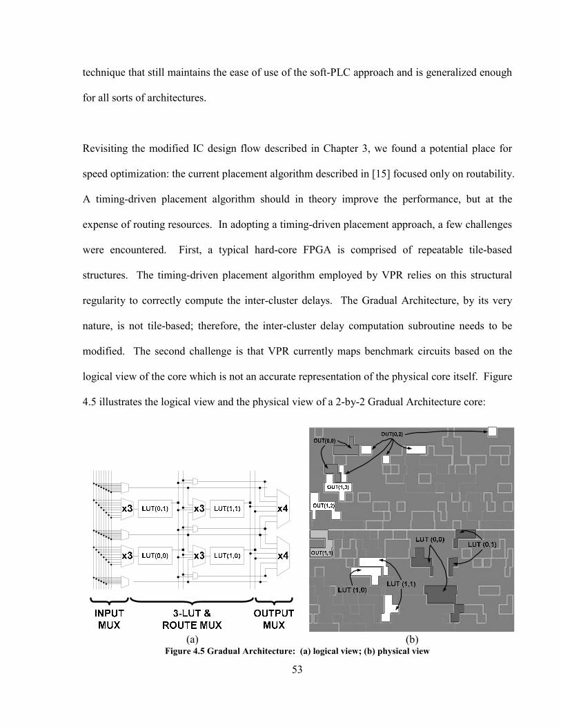
53
technique that still maintains the ease of use of the soft-PLC approach and is generalized enough
for all sorts of architectures.
Revisiting the modified IC design flow described in Chapter 3, we found a potential place for
speed optimization: the current placement algorithm described in [15] focused only on routability.
A timing-driven placement algorithm should in theory improve the performance, but at the
expense of routing resources. In adopting a timing-driven placement approach, a few challenges
were encountered. First, a typical hard-core FPGA is comprised of repeatable tile-based
structures. The timing-driven placement algorithm employed by VPR relies on this structural
regularity to correctly compute the inter-cluster delays. The Gradual Architecture, by its very
nature, is not tile-based; therefore, the inter-cluster delay computation subroutine needs to be
modified. The second challenge is that VPR currently maps benchmark circuits based on the
logical view of the core which is not an accurate representation of the physical core itself. Figure
4.5 illustrates the logical view and the physical view of a 2-by-2 Gradual Architecture core:
(a)
(b)
Figure 4.5 Gradual Architecture: (a) logical view; (b) physical view
54
The topological difference between the two views can be problematic when it comes to
computing the relative delays between two clusters. To illustrate this point, consider the two
cases shown in Figure 4.6.
Figure 4.6 Inter-CLB delays: (a) logical view; (b) physical view
When VPR computes delays, it assumes the distance from block A to B, is identical to the
distance from block A to C. All others being equal, the interconnect delay for these two pairs of
blocks should be the same (e.g., DAB=DAC=0.1ns). So the cost of choosing block B or C is the
same. The actual physical layout of the core, however, tells a different story. As indicated in
Figure 4.6(b), the cost of choosing block C would be lower than that of block B, based on the
timing difference. Without the actual timing information, VPR would not be able to make an
intelligent placement decision.
Based on the above, we made the following conjecture: if VPR were to place the benchmark
circuits based on the actual delay information extracted from the physical view of the core, the
placement quality should improve. We could also apply the same delay information to VPR’s
routing algorithm, but since the Gradual Architecture is highly routing-resource limited, a
timing-driven algorithm would more likely to result in unroutable circuits. Therefore, we
decided to focus on just placement optimization.
55
To make the current placement algorithm timing aware, we adopted the original cost function
implemented in VPR’s T-VPlace. Referring back to Figure 2.10, the cost function ∆C of the
simulated annealing placement algorithm controls the characteristics of the result produced by
VPR. The modified cost function is as follows:
CostMux PreviousCostMux )1(
Cost Timing PreviousCost Timing ∆
⋅−+∆
⋅=∆ λλC ,
where λ is a timing tradeoff factor which determines the relative importance of the cost
components and PreviousTimingCost and PreviousMuxCost are normalizing factors that are
updated once every temperature. The mux cost is the original cost function developed for the
Gradual Architecture; this component minimizes the over-use of routing resources. The timing
cost is the same as the one implemented in T-VPlace but with one exception: the connection
delay ),( jiDelay is no longer an estimated Elmore delay [49] based on the parasitic information
(i.e., R, C values) specified in the architecture description file. Instead, the connection delay is
now based on the physical delays extracted from the layout of the core.
During the physical design stage, Silicon Ensemble saves a detailed parasitic model of the core;
PrimeTime then utilizes this model to produce both wire delay and cell delay information. A
series of PERL scripts are used to automate the parsing and processing of the delay information
into a form usable by VPR. There are two major modifications to T-VPlace. First, the original
placement algorithm assumes identical intrinsic delay for each cluster block and therefore, does
not include this delay in cost calculation. This assumption is not valid with the soft-PLC
approach, so the new algorithm considers the delay through each cluster. Second, the original
placement algorithm computes the connection delay ),( jiDelay based on the relative Manhattan
56
distance between the source i and sink j (see Figure 4.7a). In this case, the upper-bound of the
lookup table that stores the connection delays between all pair of clusters is only )1()1( −×− DD ,
where D is the dimension of the core. The new algorithm, however, is based on the absolute
Cartesian coordinates of the source and the sink (see Figure 4.7b); any given pair of clusters has
its own distinct delay value. The implication of this approach is the size of the lookup table
storing the absolute delays grows quadratically with the core dimension D; the upper bound is
now 22 DD × . Since the soft-PLC approach is targeted for fine-grain programmability, we do not
expect the core size to grow beyond about 2020 × so the quadratic growth in the delay table is not
a serious issue.
Figure 4.7 Connection delay lookup: a) original; b) proposed
Once a benchmark is placed and routed by VPR, the same speed measurement technique
described in section 4.1.1 is used to obtain the functional delay. The combined speed
improvement and speed measurement flow is shown in Figure 4.8. In the next section, we will
show experimental results based on this flow and evaluate its effectiveness.
57
Figure 4.8 Speed improvement + speed measurement flow
4.1.4 Experimental Results
Under a normal experimental setup, the timing tradeoff parameter λ is varied from 0.0 to 1.0,
while allowing the channel width and/or the size of the FPGA core to grow as necessary. In our
case, the channel widths and the core size are fixed irrespective of the λ value chosen. This
constraint was set for two reasons. First, a change to the channel width or core size means we
would need to do a new layout and extract the timing information. Second, our goal is to obtain
speed improvements while still successfully mapping the benchmark circuits onto their original
core size found in Table 4.2.
To reduce noise in our experimental results, each benchmark circuit was placed and routed ten
times in VPR with different starting random seeds. Then we recorded the geometric mean of the
ten functional delays. Another option would be to pick the minimum value obtained through the
ten runs; however, since the simulated annealing algorithm was not optimally tuned for the new
cost function, the geometric mean is a better noise-reduction method.
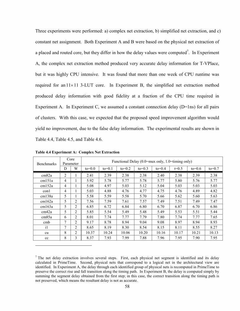
58
Three experiments were performed: a) complex net extraction, b) simplified net extraction, and c)
constant net assignment. Both Experiment A and B were based on the physical net extraction of
a placed and routed core, but they differ in how the delay values were computed7. In Experiment
A, the complex net extraction method produced very accurate delay information for T-VPlace,
but it was highly CPU intensive. It was found that more than one week of CPU runtime was
required for an 1111× 3-LUT core. In Experiment B, the simplified net extraction method
produced delay information with good fidelity at a fraction of the CPU time required in
Experiment A. In Experiment C, we assumed a constant connection delay (D=1ns) for all pairs
of clusters. With this case, we expected that the proposed speed improvement algorithm would
yield no improvement, due to the false delay information. The experimental results are shown in
Table 4.4, Table 4.5, and Table 4.6.
Table 4.4 Experiment A: Complex Net Extraction
Core Parameter Functional Delay (0.0=mux only, 1.0=timing only) Benchmarks D W to=0.0 to=0.1 to=0.2 to=0.3 to=0.4 t=0.5 to=0.6 to=0.7
cm82a 2 1 2.41 2.39 2.38 2.38 2.40 2.38 2.39 2.38 cm151a 4 1 5.92 5.78 5.77 5.78 5.77 5.80 5.76 5.77 cm152a 4 1 5.08 4.97 5.03 5.12 5.04 5.03 5.03 5.03
con1 4 1 5.03 4.88 4.76 4.77 4.75 4.76 4.89 4.82 cm138a 5 1 5.58 5.59 5.58 5.70 5.66 5.62 5.60 5.63 cm162a 5 2 7.56 7.59 7.61 7.57 7.49 7.51 7.49 7.47 cm163a 5 2 6.85 6.72 6.84 6.80 6.70 6.87 6.70 6.86 cm42a 5 2 5.85 5.54 5.49 5.48 5.49 5.53 5.51 5.44 cm85a 6 2 8.01 7.74 7.77 7.79 7.80 7.74 7.77 7.65 cmb 7 2 9.17 8.78 8.94 9.04 9.08 8.97 8.94 8.93 i1 7 2 8.65 8.19 8.30 8.54 8.15 8.11 8.55 8.27 cu 8 2 10.37 10.24 10.06 10.20 10.16 10.17 10.21 10.13 cc 8 3 8.37 7.93 7.99 7.88 7.96 7.95 7.90 7.95
7 The net delay extraction involves several steps. First, each physical net segment is identified and its delay calculated in PrimeTime. Second, physical nets that correspond to a logical net in the architectural view are identified. In Experiment A, the delay through each identified group of physical nets is recomputed in PrimeTime to preserve the correct rise and fall transition along the timing path. In Experiment B, the delay is computed simply by summing the segment delay obtained from the first step; in this case, the correct transition along the timing path is not preserved, which means the resultant delay is not as accurate.
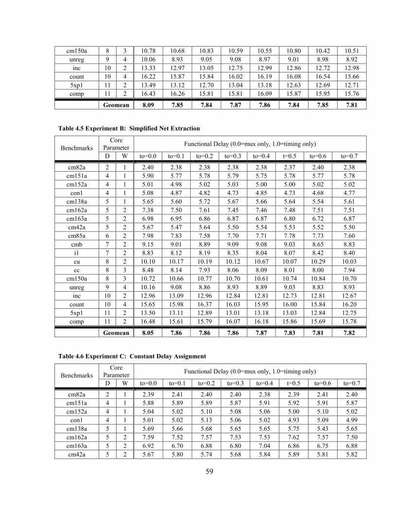
59
cm150a 8 3 10.78 10.68 10.83 10.59 10.55 10.80 10.42 10.51 unreg 9 4 10.06 8.93 9.05 9.08 8.97 9.01 8.98 8.92
inc 10 2 13.33 12.97 13.05 12.75 12.99 12.86 12.72 12.98 count 10 4 16.22 15.87 15.84 16.02 16.19 16.08 16.54 15.66 5xp1 11 2 13.49 13.12 12.70 13.04 13.18 12.63 12.69 12.71 comp 11 2 16.43 16.26 15.81 15.81 16.09 15.87 15.95 15.76
Geomean 8.09 7.85 7.84 7.87 7.86 7.84 7.85 7.81
Table 4.5 Experiment B: Simplified Net Extraction
Core Parameter Functional Delay (0.0=mux only, 1.0=timing only) Benchmarks D W to=0.0 to=0.1 to=0.2 to=0.3 to=0.4 t=0.5 to=0.6 to=0.7
cm82a 2 1 2.40 2.38 2.38 2.38 2.38 2.37 2.40 2.38 cm151a 4 1 5.90 5.77 5.78 5.79 5.75 5.78 5.77 5.78 cm152a 4 1 5.01 4.98 5.02 5.03 5.00 5.00 5.02 5.02
con1 4 1 5.08 4.87 4.82 4.73 4.85 4.73 4.68 4.77 cm138a 5 1 5.65 5.60 5.72 5.67 5.66 5.64 5.54 5.61 cm162a 5 2 7.38 7.50 7.61 7.45 7.46 7.48 7.51 7.51 cm163a 5 2 6.98 6.95 6.86 6.87 6.87 6.80 6.72 6.87 cm42a 5 2 5.67 5.47 5.64 5.50 5.54 5.53 5.52 5.50 cm85a 6 2 7.98 7.83 7.58 7.70 7.71 7.78 7.73 7.60 cmb 7 2 9.15 9.01 8.89 9.09 9.08 9.03 8.65 8.83 i1 7 2 8.83 8.12 8.19 8.35 8.04 8.07 8.42 8.40 cu 8 2 10.10 10.17 10.19 10.12 10.67 10.07 10.29 10.03 cc 8 3 8.48 8.14 7.93 8.06 8.09 8.01 8.00 7.94
cm150a 8 3 10.72 10.66 10.77 10.70 10.61 10.74 10.84 10.70 unreg 9 4 10.16 9.08 8.86 8.93 8.89 9.03 8.83 8.93
inc 10 2 12.96 13.09 12.96 12.84 12.81 12.73 12.81 12.67 count 10 4 15.65 15.98 16.37 16.03 15.95 16.00 15.84 16.20 5xp1 11 2 13.50 13.11 12.89 13.01 13.18 13.03 12.84 12.75 comp 11 2 16.48 15.61 15.79 16.07 16.18 15.86 15.69 15.78
Geomean 8.05 7.86 7.86 7.86 7.87 7.83 7.81 7.82
Table 4.6 Experiment C: Constant Delay Assignment
Core Parameter Functional Delay (0.0=mux only, 1.0=timing only) Benchmarks D W to=0.0 to=0.1 to=0.2 to=0.3 to=0.4 t=0.5 to=0.6 to=0.7
cm82a 2 1 2.39 2.41 2.40 2.40 2.38 2.39 2.41 2.40 cm151a 4 1 5.88 5.89 5.89 5.87 5.91 5.92 5.91 5.87 cm152a 4 1 5.04 5.02 5.10 5.08 5.06 5.00 5.10 5.02
con1 4 1 5.01 5.02 5.13 5.06 5.02 4.93 5.09 4.99 cm138a 5 1 5.69 5.66 5.68 5.65 5.65 5.75 5.43 5.65 cm162a 5 2 7.59 7.52 7.57 7.53 7.53 7.62 7.57 7.50 cm163a 5 2 6.92 6.70 6.88 6.80 7.04 6.86 6.75 6.88 cm42a 5 2 5.67 5.80 5.74 5.68 5.84 5.89 5.81 5.82
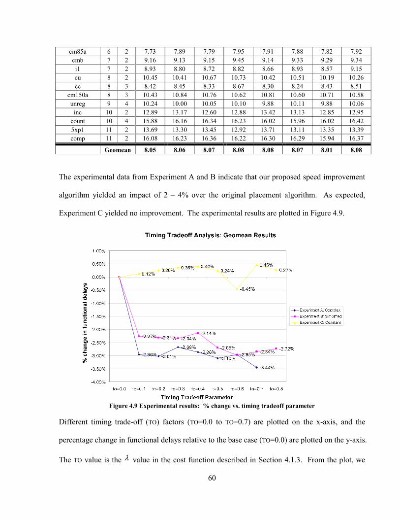
60
cm85a 6 2 7.73 7.89 7.79 7.95 7.91 7.88 7.82 7.92 cmb 7 2 9.16 9.13 9.15 9.45 9.14 9.33 9.29 9.34 i1 7 2 8.93 8.80 8.72 8.82 8.66 8.93 8.57 9.15 cu 8 2 10.45 10.41 10.67 10.73 10.42 10.51 10.19 10.26 cc 8 3 8.42 8.45 8.33 8.67 8.30 8.24 8.43 8.51
cm150a 8 3 10.43 10.84 10.76 10.62 10.81 10.60 10.71 10.58 unreg 9 4 10.24 10.00 10.05 10.10 9.88 10.11 9.88 10.06
inc 10 2 12.89 13.17 12.60 12.88 13.42 13.13 12.85 12.95 count 10 4 15.88 16.16 16.34 16.23 16.02 15.96 16.02 16.42 5xp1 11 2 13.69 13.30 13.45 12.92 13.71 13.11 13.35 13.39 comp 11 2 16.08 16.23 16.36 16.22 16.30 16.29 15.94 16.37
Geomean 8.05 8.06 8.07 8.08 8.08 8.07 8.01 8.08
The experimental data from Experiment A and B indicate that our proposed speed improvement
algorithm yielded an impact of 2 – 4% over the original placement algorithm. As expected,
Experiment C yielded no improvement. The experimental results are plotted in Figure 4.9.
Figure 4.9 Experimental results: % change vs. timing tradeoff parameter
Different timing trade-off (TO) factors (TO=0.0 to TO=0.7) are plotted on the x-axis, and the
percentage change in functional delays relative to the base case (TO=0.0) are plotted on the y-axis.
The TO value is the λ value in the cost function described in Section 4.1.3. From the plot, we
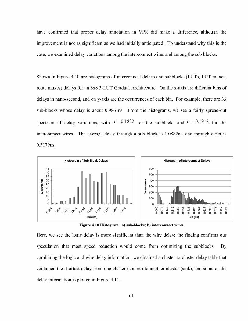
61
have confirmed that proper delay annotation in VPR did make a difference, although the
improvement is not as significant as we had initially anticipated. To understand why this is the
case, we examined delay variations among the interconnect wires and among the sub blocks.
Shown in Figure 4.10 are histograms of interconnect delays and subblocks (LUTs, LUT muxes,
route muxes) delays for an 8x8 3-LUT Gradual Architecture. On the x-axis are different bins of
delays in nano-second, and on y-axis are the occurrences of each bin. For example, there are 33
sub-blocks whose delay is about 0.986 ns. From the histograms, we see a fairly spread-out
spectrum of delay variations, with 1822.0=σ for the subblocks and 1918.0=σ for the
interconnect wires. The average delay through a sub block is 1.0882ns, and through a net is
0.3179ns.
Histogram of Sub Block Delays
05
1015202530354045
0.581
0.682
0.784
0.885
0.986
1.088
1.189
1.290
1.392
1.493
Bin (ns)
Occ
urre
nce
Histogram of Interconnect Delays
0
100
200
300
400
500
600
0.00
0
0.07
1
0.14
2
0.21
2
0.28
3
0.35
4
0.42
5
0.49
6
0.56
7
0.63
7
0.70
8
0.77
9
0.85
0
0.92
1
Bin (ns)
Occ
urre
nce
Figure 4.10 Histogram: a) sub-blocks; b) interconnect wires
Here, we see the logic delay is more significant than the wire delay; the finding confirms our
speculation that most speed reduction would come from optimizing the subblocks. By
combining the logic and wire delay information, we obtained a cluster-to-cluster delay table that
contained the shortest delay from one cluster (source) to another cluster (sink), and some of the
delay information is plotted in Figure 4.11.
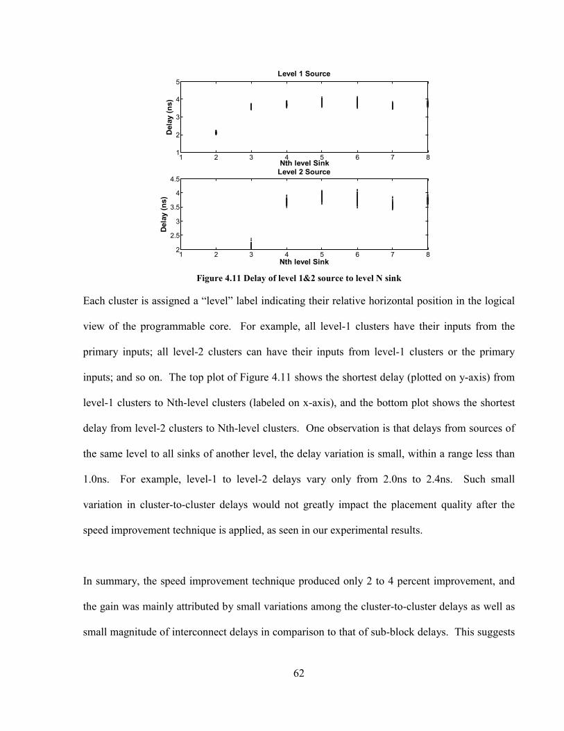
62
1 2 3 4 5 6 7 81
2
3
4
5Level 1 Source
Nth level SinkD
elay
(ns)
1 2 3 4 5 6 7 82
2.5
3
3.5
4
4.5Level 2 Source
Nth level Sink
Del
ay (n
s)
Figure 4.11 Delay of level 1&2 source to level N sink
Each cluster is assigned a “level” label indicating their relative horizontal position in the logical
view of the programmable core. For example, all level-1 clusters have their inputs from the
primary inputs; all level-2 clusters can have their inputs from level-1 clusters or the primary
inputs; and so on. The top plot of Figure 4.11 shows the shortest delay (plotted on y-axis) from
level-1 clusters to Nth-level clusters (labeled on x-axis), and the bottom plot shows the shortest
delay from level-2 clusters to Nth-level clusters. One observation is that delays from sources of
the same level to all sinks of another level, the delay variation is small, within a range less than
1.0ns. For example, level-1 to level-2 delays vary only from 2.0ns to 2.4ns. Such small
variation in cluster-to-cluster delays would not greatly impact the placement quality after the
speed improvement technique is applied, as seen in our experimental results.
In summary, the speed improvement technique produced only 2 to 4 percent improvement, and
the gain was mainly attributed by small variations among the cluster-to-cluster delays as well as
small magnitude of interconnect delays in comparison to that of sub-block delays. This suggests
63
it is difficult to make substantial timing improvements for soft cores generated using VPR and
the ASIC design flow.
4.2 Power Considerations
Power consumption is becoming a major concern in IC designs. This section first describes a
method of measuring power consumed by soft-PLC cores. Then, it presents the power overhead
of using soft-PLC to implement the benchmarks vs. the equivalent ASIC implementation.
4.2.1 Power Measurement Methodology
Several power models for FPGAs have been developed in recent years [51][52]. However, these
FPGA power models are not directly applicable to the soft cores since they are not regularly
shaped architectures. For these reasons, we have adopted a different power analysis tool: the
Synopsys PrimePower. PrimePower is a “dynamic gate-level simulation and analysis tool
that accurately analyzes power dissipation of cell-based designs” [53]. PrimePower is comprised
of two stages: HDL simulation to generate switch activity file, and power profile building. In
our experiment, Verilog-XL is used to generate the switch activity file in VCD (value change
dump) format; the gate-level simulation is back-annotated with the SDF file of the design in
interest. In the second stage, the VCD file, the HDL of the design, the SDF file, and the
technology library data are utilized by PrimePower to build the power profile and produce the
power report. Figure 4.12 illustrates the flow for both the ASIC implementation and the soft-
PLC implementation of the benchmarks selected for this experiment.
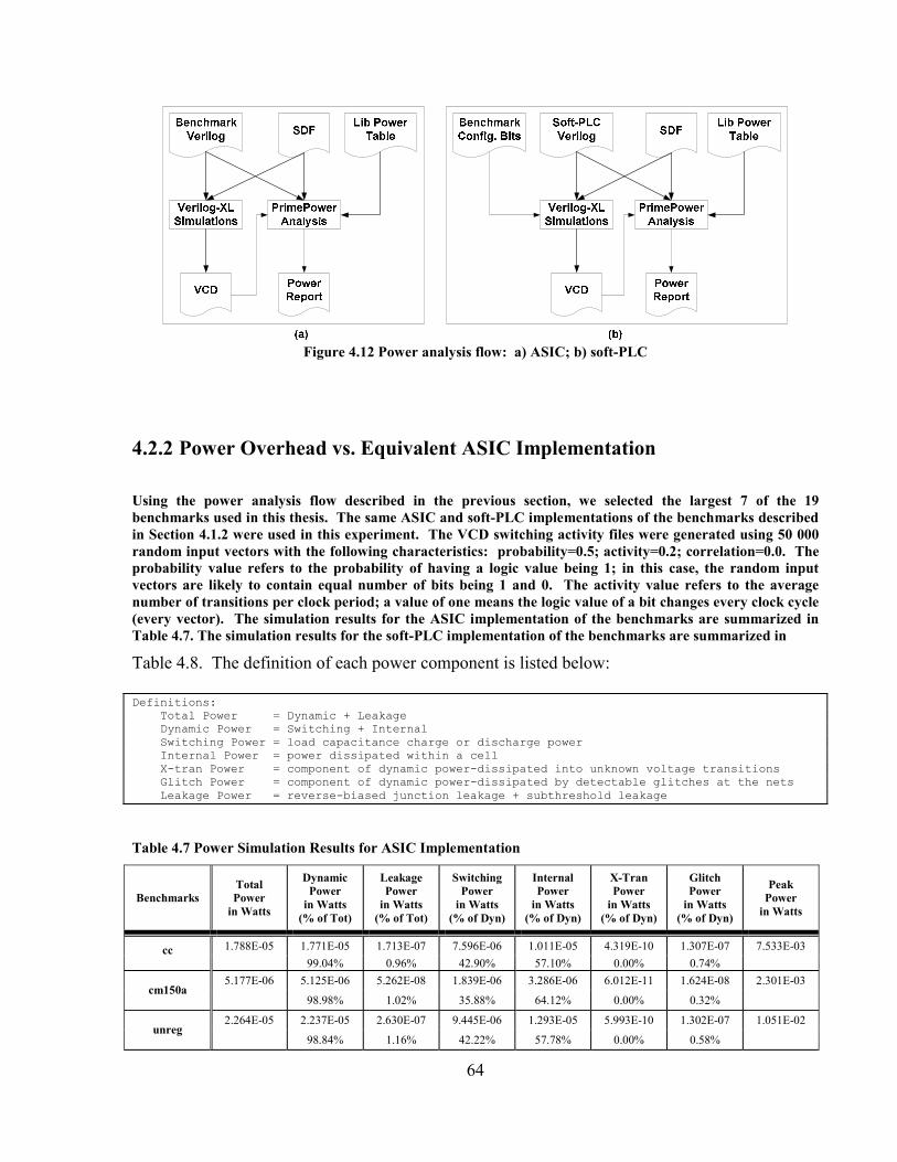
64
Figure 4.12 Power analysis flow: a) ASIC; b) soft-PLC
4.2.2 Power Overhead vs. Equivalent ASIC Implementation
Using the power analysis flow described in the previous section, we selected the largest 7 of the 19 benchmarks used in this thesis. The same ASIC and soft-PLC implementations of the benchmarks described in Section 4.1.2 were used in this experiment. The VCD switching activity files were generated using 50 000 random input vectors with the following characteristics: probability=0.5; activity=0.2; correlation=0.0. The probability value refers to the probability of having a logic value being 1; in this case, the random input vectors are likely to contain equal number of bits being 1 and 0. The activity value refers to the average number of transitions per clock period; a value of one means the logic value of a bit changes every clock cycle (every vector). The simulation results for the ASIC implementation of the benchmarks are summarized in Table 4.7. The simulation results for the soft-PLC implementation of the benchmarks are summarized in
Table 4.8. The definition of each power component is listed below:
Definitions: Total Power = Dynamic + Leakage Dynamic Power = Switching + Internal Switching Power = load capacitance charge or discharge power Internal Power = power dissipated within a cell X-tran Power = component of dynamic power-dissipated into unknown voltage transitions Glitch Power = component of dynamic power-dissipated by detectable glitches at the nets Leakage Power = reverse-biased junction leakage + subthreshold leakage
Table 4.7 Power Simulation Results for ASIC Implementation
Benchmarks Total Power
in Watts
Dynamic Power
in Watts (% of Tot)
Leakage Power
in Watts (% of Tot)
Switching Power
in Watts (% of Dyn)
Internal Power
in Watts (% of Dyn)
X-Tran Power
in Watts (% of Dyn)
Glitch Power
in Watts (% of Dyn)
Peak Power
in Watts
1.788E-05 1.771E-05 1.713E-07 7.596E-06 1.011E-05 4.319E-10 1.307E-07 7.533E-03 cc 99.04% 0.96% 42.90% 57.10% 0.00% 0.74%
5.177E-06 5.125E-06 5.262E-08 1.839E-06 3.286E-06 6.012E-11 1.624E-08 2.301E-03 cm150a
98.98% 1.02% 35.88% 64.12% 0.00% 0.32%
2.264E-05 2.237E-05 2.630E-07 9.445E-06 1.293E-05 5.993E-10 1.302E-07 1.051E-02 unreg
98.84% 1.16% 42.22% 57.78% 0.00% 0.58%
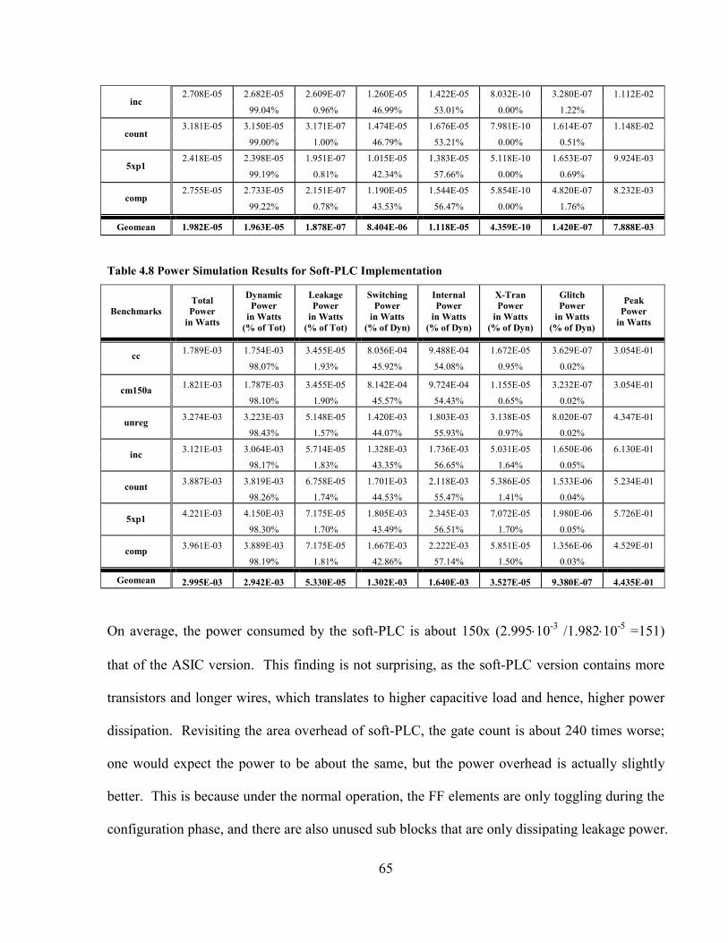
65
2.708E-05 2.682E-05 2.609E-07 1.260E-05 1.422E-05 8.032E-10 3.280E-07 1.112E-02 inc
99.04% 0.96% 46.99% 53.01% 0.00% 1.22%
3.181E-05 3.150E-05 3.171E-07 1.474E-05 1.676E-05 7.981E-10 1.614E-07 1.148E-02 count
99.00% 1.00% 46.79% 53.21% 0.00% 0.51%
2.418E-05 2.398E-05 1.951E-07 1.015E-05 1.383E-05 5.118E-10 1.653E-07 9.924E-03 5xp1
99.19% 0.81% 42.34% 57.66% 0.00% 0.69%
2.755E-05 2.733E-05 2.151E-07 1.190E-05 1.544E-05 5.854E-10 4.820E-07 8.232E-03 comp
99.22% 0.78% 43.53% 56.47% 0.00% 1.76%
Geomean 1.982E-05 1.963E-05 1.878E-07 8.404E-06 1.118E-05 4.359E-10 1.420E-07 7.888E-03
Table 4.8 Power Simulation Results for Soft-PLC Implementation
Benchmarks Total Power
in Watts
Dynamic Power
in Watts (% of Tot)
Leakage Power
in Watts (% of Tot)
Switching Power
in Watts (% of Dyn)
Internal Power
in Watts (% of Dyn)
X-Tran Power
in Watts (% of Dyn)
Glitch Power
in Watts (% of Dyn)
Peak Power
in Watts
1.789E-03 1.754E-03 3.455E-05 8.056E-04 9.488E-04 1.672E-05 3.629E-07 3.054E-01 cc 98.07% 1.93% 45.92% 54.08% 0.95% 0.02%
1.821E-03 1.787E-03 3.455E-05 8.142E-04 9.724E-04 1.155E-05 3.232E-07 3.054E-01 cm150a 98.10% 1.90% 45.57% 54.43% 0.65% 0.02%
3.274E-03 3.223E-03 5.148E-05 1.420E-03 1.803E-03 3.138E-05 8.020E-07 4.347E-01 unreg 98.43% 1.57% 44.07% 55.93% 0.97% 0.02%
3.121E-03 3.064E-03 5.714E-05 1.328E-03 1.736E-03 5.031E-05 1.650E-06 6.130E-01 inc 98.17% 1.83% 43.35% 56.65% 1.64% 0.05%
3.887E-03 3.819E-03 6.758E-05 1.701E-03 2.118E-03 5.386E-05 1.533E-06 5.234E-01 count 98.26% 1.74% 44.53% 55.47% 1.41% 0.04%
4.221E-03 4.150E-03 7.175E-05 1.805E-03 2.345E-03 7.072E-05 1.980E-06 5.726E-01 5xp1 98.30% 1.70% 43.49% 56.51% 1.70% 0.05%
3.961E-03 3.889E-03 7.175E-05 1.667E-03 2.222E-03 5.851E-05 1.356E-06 4.529E-01 comp 98.19% 1.81% 42.86% 57.14% 1.50% 0.03%
Geomean 2.995E-03 2.942E-03 5.330E-05 1.302E-03 1.640E-03 3.527E-05 9.380E-07 4.435E-01
On average, the power consumed by the soft-PLC is about 150x (2.995⋅10-3 /1.982⋅10-5 =151)
that of the ASIC version. This finding is not surprising, as the soft-PLC version contains more
transistors and longer wires, which translates to higher capacitive load and hence, higher power
dissipation. Revisiting the area overhead of soft-PLC, the gate count is about 240 times worse;
one would expect the power to be about the same, but the power overhead is actually slightly
better. This is because under the normal operation, the FF elements are only toggling during the
configuration phase, and there are also unused sub blocks that are only dissipating leakage power.
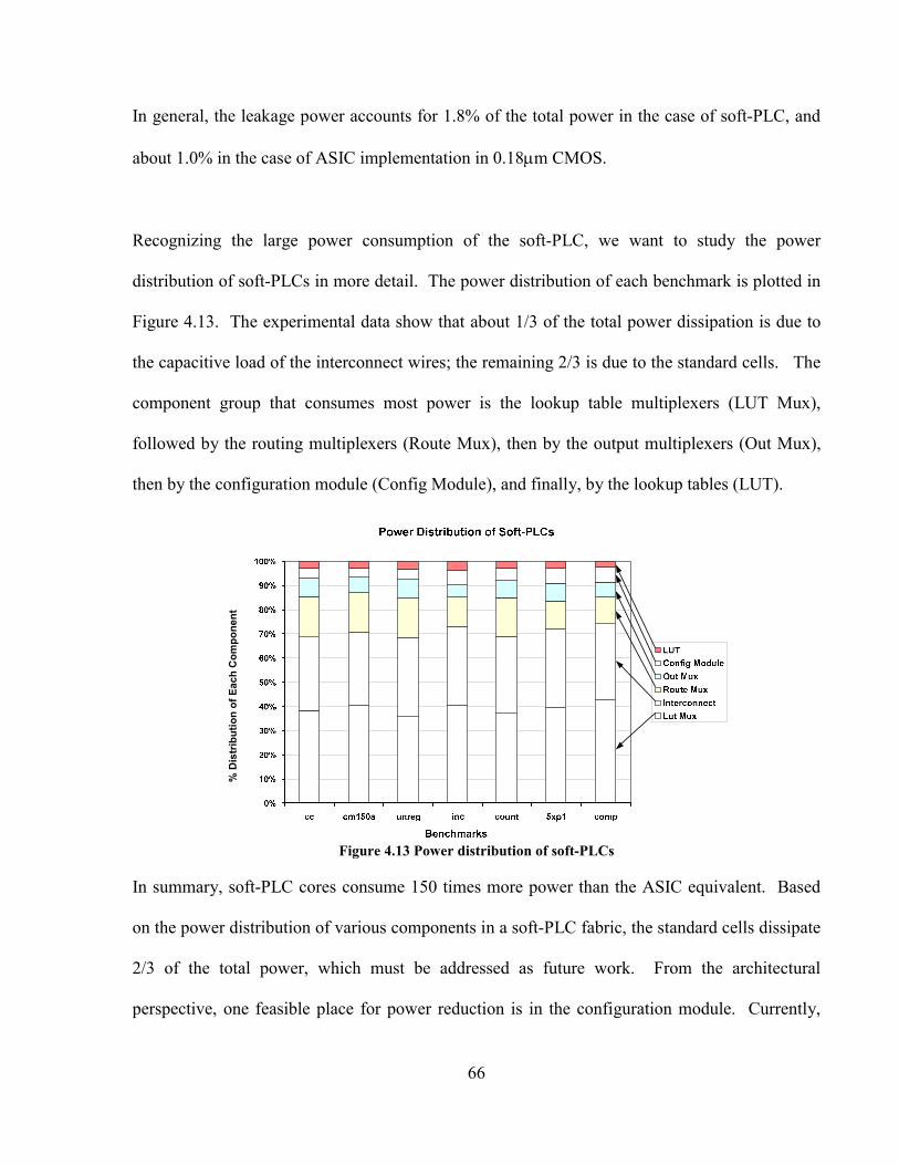
66
In general, the leakage power accounts for 1.8% of the total power in the case of soft-PLC, and
about 1.0% in the case of ASIC implementation in 0.18µm CMOS.
Recognizing the large power consumption of the soft-PLC, we want to study the power
distribution of soft-PLCs in more detail. The power distribution of each benchmark is plotted in
Figure 4.13. The experimental data show that about 1/3 of the total power dissipation is due to
the capacitive load of the interconnect wires; the remaining 2/3 is due to the standard cells. The
component group that consumes most power is the lookup table multiplexers (LUT Mux),
followed by the routing multiplexers (Route Mux), then by the output multiplexers (Out Mux),
then by the configuration module (Config Module), and finally, by the lookup tables (LUT).
% D
istr
ibut
ion
of E
ach
Com
pone
nt
Figure 4.13 Power distribution of soft-PLCs
In summary, soft-PLC cores consume 150 times more power than the ASIC equivalent. Based
on the power distribution of various components in a soft-PLC fabric, the standard cells dissipate
2/3 of the total power, which must be addressed as future work. From the architectural
perspective, one feasible place for power reduction is in the configuration module. Currently,
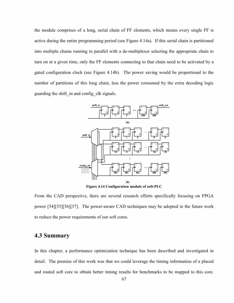
67
the module comprises of a long, serial chain of FF elements, which means every single FF is
active during the entire programming period (see Figure 4.14a). If this serial chain is partitioned
into multiple chains running in parallel with a de-multiplexer selecting the appropriate chain to
turn on at a given time, only the FF elements connecting to that chain need to be activated by a
gated configuration clock (see Figure 4.14b). The power saving would be proportional to the
number of partitions of this long chain, less the power consumed by the extra decoding logic
guarding the shift_in and config_clk signals.
Figure 4.14 Configuration module of soft-PLC
From the CAD perspective, there are several research efforts specifically focusing on FPGA
power [54][55][56][57]. The power-aware CAD techniques may be adopted in the future work
to reduce the power requirements of our soft cores.
4.3 Summary
In this chapter, a performance optimization technique has been described and investigated in
detail. The premise of this work was that we could leverage the timing information of a placed
and routed soft core to obtain better timing results for benchmarks to be mapped to this core.

68
Our results showed only 2 to 4 percent improvements over nineteen benchmark circuits. This
technique could be useful if timing requirement is critical.
The power overhead of using a soft core has also been discussed in this chapter. Using Synopsys
PrimePower tool, we were able to obtain high fidelity power simulation results; based on the
results, the overhead of using a soft core is about 150 times relative to the ASIC implementation.
69
Chapter 5
Conclusions and Future Work
5.1 Summary
In this thesis we have investigated the feasibility of integrating a synthesizable programmable
logic core (soft-PLC) into a fixed ASIC design, and we have accurately measured the area, speed
and power overhead of implementing circuits in such cores. Future SoCs are likely to be shipped
with embedded programmable logic cores; these programmable cores provide SoCs with the
ability to easily adapt to changing standards, to span a family of products, or to correct design
errors without creating a new mask set. Currently, these FPGA-like programmable cores are
commercially available in the form of custom layout macros (“hard” core) from third party
vendors. An alternative approach to embedded programmability in SoCs is to create
synthesizable programmable logic cores (“soft” cores) that are described in HDL languages and
can be synthesized and laid out using the existing CAD tools for ASIC designs. With the
architecture and optimized VPR tool for the soft-core approach already in place, our goal was to
validate this approach through chip implementation, as well as investigate any speed and power
issues.
70
This thesis began with the implementation of an integrated circuit containing a synthesizable
programmable logic core, and in doing so, has illustrated some of the issues that arise when such
a core is used. One issue involved the size of the programmable logic core selected. If a core is
too small, it will be unable to implement logic functions that may be required in the future. In
our integrated circuit, although we estimated that forty-nine 3-LUTs would be enough to
implement a variety of next state functions, we chose a sixty-four 3-LUT architecture. Similarly,
we chose a core with more inputs and outputs than we expected to use. These two issues apply
to both “hard” programmable logic cores and synthesizable logic cores. The third issue was
concerned with the clock-tree generation for the configuration module, and this difficulty was
specific to synthesizable programmable logic cores. The soft core placed an extra burden on the
clock-tree synthesis as the configuration clock drives a large number of serially chained flip-
flops, which reduced the overall density of the chip. Further study also revealed that an incorrect
clock constraint during the front-end synthesis stage could cause unnecessary buffers to be
inserted between each FF.
Through the chip implementation, we observed that the area penalty of the soft core was about
560x, and the entire chip slowed down by more than 2x. This prompted further investigation
into the area, speed and power overhead of using the soft-core approach. A total of 19
benchmark circuits were used in our experiments; for each benchmark, we chose the smallest
core on which it could fit. The same 19 benchmark circuits were also implemented as fixed
ASIC logic and used as a reference. On average, the area overhead of the soft-core approach
was found to be 200x, the speed overhead 10x, and power overhead 150x. The overheads
71
observed were largely due to the use of standard cells that are inherently area, speed and power
inefficient.
To address the performance issue, we proposed a new speed optimization technique that allowed
the VPR tool to take timing into consideration during placement. The challenge in making the
placement algorithm “timing-aware” was to accurately extract the delay values from the soft-
PLC’s physical layout and “annotate” these values in VPR. Unlike a tile-based FPGA, delay
values of a soft-PLC could not be computed the same way in VPR; the values must be obtained
from a timing-analysis tool, based on the physical layout of the core. Our goal was to improve
the timing of mapped circuits without paying extra penalty on area (routing fabric). Given this
constraint, it was found that our performance optimization technique could improve the speed by
2 - 4%. This improvement range was lower than initially anticipated, given that we observed a
great variation in net delays when nets were examined individually. However, when we
examined the pin-to-pin delay from source LUTs to sink LUTs, the delay variations became less
prominent. Also, the programmable cores were optimized for speed during synthesis, and laid
out in a square shape during the physical design. In a real application where the programmable
core is synthesized and laid out together with other IP cores, we expect a greater variation in
delay values; in this case, our speed optimization technique should have greater impact.
5.2 Future Work
As our work shows, using a “soft” core incurs a significant area, speed and power overhead. A
main source of this overhead is that standard generic ASIC cells are not optimized for any
specific architecture. For example, the standard-cell library used in this thesis contained only
72
two types of multiplexers with different driving strengths: 2-to-1 and 4-to-1 multiplexers.
Considering most of the multiplexers in the Gradual Architecture have large inputs (some as
large as 32 inputs), it is not efficient to build these large multiplexers with small multiplexers and
other logic cells, because the driving strength of each cell is not perfectly matched when they are
put together to form a larger logic module. Also, the configuration FFs can be replaced with
custom-designed SRAM bits. By creating custom cells we could obtain significant savings in
area, speed, and power. These custom cells can be made part of the standard-cell library and
utilized by the synthesis tool as building blocks for synthesizable programmable cores.
Another issue that we have not examined is power reduction techniques for synthesizable
programmable cores. The power optimization can be achieved at physical design level; creating
custom cells could lower both dynamic and static power, if transistor sizing is done appropriately.
As leakage current is a major concern for the future technology nodes, static power dissipation
could be minimized by techniques such as fixing the threshold voltage, VT, at a higher value, but
this limits the performance due to a reduced (VDD-VT) gate overdrive term. At a higher level, the
power optimization could be achieved by employing “power-aware” FPGA CAD tools on soft
cores. However, the gains obtained from “power-aware” CAD tools might not be high, since the
soft-core approach is aimed at fine-grained programmability.
5.3 Contributions
The contributions of this work are summarized as follows:
1. We implemented a test-chip on silicon containing a synthesizable programmable core
that interacts with the fixed ASIC logic portion of the test-chip. Through functional
73
testing with two separate modes of programming, we validated the concept of using
“soft” programmable logic cores in SoC applications and showed it to be viable.
2. We accurately measured the area density, speed efficiency and power consumption of
using the soft-core approach and compared these values to the equivalent ASIC
implementation. The area density was obtained from the physical implementation; the
speed efficiency was obtained from the static timing analysis based on the physical
implementation; and the power consumption was obtained from the power analysis tool
based on the dynamic timing simulation of the physical implementation.
3. We proposed a novel speed optimization technique suitable for the soft-core approach.
This technique exploits the delay reporting capability of the PrimeTime tool to extract
the logic and net delays of the physical implementation of a soft core. The raw delay
information was processed through a series of scripts and utilities to create a delay lookup
table. A new “timing-aware” algorithm was developed and integrated into VPR that
utilizes the delay lookup table to allow user circuits to be efficiently placed and routed on
the soft-core architectures.
74
REFERENCE
[1] S. Thompson, M. Alavi, M. Hussein, P. Jacob, C. Kenyon, P. Moon, M. Prince, S. Sivakumar, S. Tyagi and M. Bohr, "130nm Logic Technology Featuring 60nm Transistors, Low-K Dielectrics, and Cu Interconnects." Intel Technology Journal. vol. 6, issue. 2, May 2002.
[2] P. Silverman, "The Intel Lithography Roadmap”, Intel Technology Journal, vol. 6, issue. 2, May 2002.
[3] “IC makers brace for $3 million mask at 65 nm”, EETIMES article, September 2003. http://www.eetimes.com/showArticle.jhtml?articleID=18309458
[4] J. Greenbaum, “Reconfigurable Logic in SoC Systems”, Proceedings of the 2002 Custom Integrated Circuits Conference, pp. 5-8.
[5] eASIC, “eASICore® 0.18µm Process”, http://www.easic.com/products/easicore018.html
[6] Leopard Logic, “Gladiator CLD6400”, http://www.leopardlogic.com/
[7] Actel Corp., “VariCore™ Embedded Programmable Gate Array Core (EPGA™) 0.18µ Family”, Datasheet, http://www.actel.com/varicore/products/index.html
[8] M2000, Inc., “M2000 FlexEOS Core”, http://www.m2000.fr/products.htm
[9] “Panel debates merits of embedded FPGA megacells”, EETIMES article, March 2001. http://www.eetuk.com/showArticle.jhtml?articleID=17407115
[10] N. Kafafi, K. Bozman, S.J.E. Wilton, “Architectures and Algorithms for Synthesizable Embedded Programmable Logic Cores”, Proceedings of the ACM International Symposium on Field-Programmable Gate Arrays, Monterey, CA, pp. 1-9, Feb 2003.
[11] S.J.E. Wilton, R. Saleh, “Programmable Logic IP Cores in SoC Design: Opportunities and Challenges”, Proceedings of the 2001Custom Integrated Circuits Conference, pp. 63-66.
[12] M. Borgatti, F. Lertora, B. Foret, L. Cali, “A Reconfigurable System featuring Dynamically Extensible Embedded Microprocessor, FPGA, and Customisable I/O”, IEEE Journal of Solid-State Circuits, vol. 38, no. 3, pp. 521-529, March 2003.
[13] T. Vaida, “PLC Advanced Technology Demonstrator TestChipB”, Proceedings of the 2001 Custom Integrated circuits conference, pp. 67-70, May 2001.
[14] S. Knapp, D. Tavana, “Field configurable system-on-chip device architecture” Proceedings of the IEEE 2000 Custom Integrated Circuits Conference, pp. 155–158, May 2000.
75
[15] N. Kafafi, “Architecture and Algorithms for Synthesizable Embedded Programmable Logic Cores”, M.A.Sc. thesis, Dept. of Comp. and Elect. Eng., Univ. of British Columbia, Vancouver, BC, 2004.
[16] Keating, Michael, and Pierre Bricaud. Reuse Methodology Manual. Boston: Kluwer Academic Publishers, 1999.
[17] A. Yan, S.J.E. Wilton, “Product Term Embedded Synthesizable Logic Cores”, in the IEEE International Conference on Field-Programmable Technology, Tokyo, Japan, pp. 162-169, Dec. 2003.
[18] Canadian Microelectronics Corporation, “Tutorial on CMC’s Digital IC Design Flow”, Document ICI-096, Part of Tutorial Release V1.3, May 2001.
[19] Synopsys, HDL Compiler for VHDL Reference Manual, v2002.05
[20] Synopsys, DC Ultra Datasheet, v2002.05, http://www.synopsys.com/
[21] Cadence, Encounter RTL Compiler Datasheet, http://www.cadence.com/
[22] Magma Design Automation, Blast Create Datasheet, http://www.magma-da.com/
[23] J. Rose, R.J. Francis, D. Lewis, and P. Chow, “Architecture of Field-Programmable Gate Arrays: The Effect of Logic Functionality on Area Efficiency”, IEEE Journal of Solid-State Circuits, 1990.
[24] E. Ahmed and J. Rose, “The effect of LUT and Cluster Size on Deep-Submicron FPGA Performance and Density”, ACM International Symposium on Field-Programmable Gate Arrays, pp. 3-12, 2001.
[25] Altera Corp., Stratix II Device Handbook, Vol. 1, San Jose, CA, pp. 2-6 – 2-7, 2004
[26] V. Betz and J. Rose, “VPR: A New Packing, Placement and Routing Tool for FPGA Research,” Seventh International Workshop on Field-Programmable Logic and Applications, London, UK, pp. 213–222, 1997
[27] V. Betz, J. Rose, and A. Marquardt, “Architecture and CAD for Deep-Submicron FPGAs”, Kluwer Academic Publishers, 1999.
[28] A. Dunlop and B. Kernighan, “A Procedure for Placement of Standard-Cell VLSI Circuits”, IEEE Transactions on CAD, pp. 196-173, January 1985.
[29] D. Huang and A. Kahng, “Partioning-Based Standard-Cell Global Placement with an Exact Objective”, ACM Symposium on Physical Design, pp. 18-25, 1997
[30] S. Hauck and G. Borriello, “An Evaluation of Bipartitioning Techniques”, Proceedings of the 16th Conference on Advanced Research in VLSI, pp. 383-402, 1995
76
[31] B. Riess, and G. Ettelt, “Speed: Fast and Efficient Timing Driven Placement”, IEEE Symposium on Circuits and Systems, pp.377-380, 1995.
[32] G. Sigl, K. Doll, and F. Johannes, “Analytical Placement: A Linear or a Quadratic Programming and Slicing Optimization”, in Proceedings ACM/IEEE Design Automation Conference, pp. 427-432, 1991
[33] A. Marquardt, V. Betz, and J. Rose, “Timing-Driven Placement for FPGAs”, ACM International Symposium on Field-Programmable Gate Arrays, Monterey, CA, pp. 203-213, February 2000.
[34] S. Kirkpatrick, C. Gelatt, and M. Vecchi, “Optimization by Simulated Annealing”, Science, pp. 671-680, 1983.
[35] C. Sechen and A. Sangiovanni-Vincentelli, “TimberWolf Placement and Routing Package”, JSSC, pp. 510-522, 1985.
[36] M. Huang, F. Romeo, and A. Sangiovanni-Vincentelli, “An Efficient General Cooling Schedule for Simulated Annealing”, International Conference on Computer Aided Design, pp. 381-384, 1986.
[37] L. McMurchie, and C. Ebeling, “PathFinder: A Negotiation-Based Performance-Driven Router for FPGAs”, ACM/SIGDA International Symposium on Field-Programmable Gate Arrays, Monterey, CA, pp. 111-117, February 1995.
[38] Victor O. Aken’Ova, “A Parallel Core Access Interface for Test”, EECE 578 Internal Report, April 2002.
[39] Mohsen Nahvi, Andre Ivanov, “A Packet Switching Communication-Based Test Access Mechanism for System Chips”, Proc. IEEE European Test Workshop, 2001, pp. 81 - 86.
[40] Altera Corp., Max+Plus II Baseline Software, http://www.altera.com
[41] Paul Leventis, “Using edif2blif Version 1.0”, June 30, 1998 http://www.eecg.toronto.edu/~jayar/software/edif2blif/user.pdf
[42] E. Sentovich et al. “SIS: a system for sequential circuit synthesis.” Tech. Report No. UCB/ERL M92/41, University of California at Berkeley, 1992.
[43] K.C. Chen, J. Cong, Y. Ding, A.B. Kahng, and P. Trajmar, “DAG-Map: Graph-Based FPGA Technology Mapping for Delay Optimization”, IEEE Design and Test of Computers, pp.7-20, September 1992.
[44] A. Marquardt, V. Betz, and J. Rose, “Using Cluster-based Logic Blocks and Timing-Driven Packing to Improve FPGA Speed and Density”, ACM International Symposium on Field-Programmable Gate Arrays, pp. 37-46, February 1999.
[45] Synopsys, “Chapter 8 Optimizing the Design”, Design Compiler User Guide, v2002.05
77
[46] “Taxonomy of functional verification for virtual component development and integration”, EEdesign article, January 2001.
[47] Virtual Silicon Technology Inc., “Silicon Ready [tm] Product Information – Diplomat-18[tm] High Performance Standard Cells”, Sunnyvale, CA, 1998.
[48] Synopsys, PrimeTime User Guide: Advanced Timing Analysis, Ver. T-2002.09
[49] D. A. Hodges, H. G. Jackson and R. Saleh, Analysis and Design of Digital Integrated Circuits, Third Edition, McGraw-Hill, 2003
[50] S. Yang, “Logic Synthesis and Optimization Benchmarks, Version 3.0”, Tech. Report, Microelectronic Center of North Carolina, 1991.
[51] K. Poon, A. Yan, S.J.E. Wilton, “A Flexible Power Model for FPGAs”, to appear in 12th International Conference on Field-Programmable Logic and Applications, September 2002
[52] F. Li, D. Chen, L. He, J. Cong, “Architecture Evaluation for Power-Efficient FPGAs”, in the ACM International Symposium on Field-Programmable Gate Arrays, Monterey, CA, pp. 175 – 184, February 2003
[53] Synopsys, PrimePower Manual, Version 2002.05
[54] J. Lamoureux, S.J.E. Wilton, “On the interaction between power-aware FPGA CAD Algorithms”, in the International Conference on Computer Aided Design, pp. 701 – 708, November 2003
[55] J. Anderson, and F.N. Najm, “Power-Aware Technology Mapping for LUT-Based FPGAs”, IEEE International Conference on Field-Programmable Technology, pp. 211-218, December 2002.
[56] A. Singh, and M. Malgorzata, “Efficient Circuit Clustering for Area and Power Reduction in FPGAs”, Proc. ACM International Symposium on Field-Programmable Gate Arrays, Monterey, CA, pp. 59-66, February 2002.
[57] H. Li, W-K. Mak, and S. Katkoori, “LUT-Based FPGA Technology Mapping for Power Minimization with Optimal Depth”, IEEE Computer Society Workshop on VLSI, Orlando, pp.123-128, 2001.