hmc1099pm5e | 10 w (40 dbm), 0.01 ghz to 1.1 ghz, gan
TRANSCRIPT

10 W (40 dBm), 0.01 GHz to 1.1 GHz, GaN Power Amplifier
Data Sheet HMC1099PM5E
Rev. B Document Feedback Information furnished by Analog Devices is believed to be accurate and reliable. However, no responsibility is assumed by Analog Devices for its use, nor for any infringements of patents or other rights of third parties that may result from its use. Specifications subject to change without notice. No license is granted by implication or otherwise under any patent or patent rights of Analog Devices. Trademarks and registered trademarks are the property of their respective owners.
One Technology Way, P.O. Box 9106, Norwood, MA 02062-9106, U.S.A. Tel: 781.329.4700 ©2018 Analog Devices, Inc. All rights reserved. Technical Support www.analog.com
FEATURES High small signal gain: 20 dB typical POUT: 41.5 dBm typical at PIN = 27 dBm High PAE: 60% typical at PIN = 27 dBm Instantaneous bandwidth: 0.01 GHz to 1.1 GHz across all
frequencies Supply voltage: VDD = 28 V at a quiescent current of 100 mA Internal prematching
Simple and compact external tuning for optimal performance
5 mm × 5 mm, 32-lead LFCSP
APPLICATIONS Extended battery operation for public mobile radios Power amplifier stage for wireless infrastructures Test and measurement equipment Commercial and military radars General-purpose transmitter amplification
FUNCTIONAL BLOCK DIAGRAM
17
1
34
2GNDNICNIC
RFIN/VGG56
RFIN/VGGNIC
7NIC8GND GND
18 NIC19 NIC20 RFOUT/VDD
21 RFOUT/VDD
22 NIC23 NIC
NIC = NO INTERNAL CONNECTION. THESE PINSARE NOT CONNECTED INTERNALLY.
24 GND
GN
D
NIC
NIC
NIC
NIC
NIC
NIC
GN
DG
ND
NIC
NIC
NIC
NIC
NIC
NIC
GN
D
PACKAGEBASE
1682
6-00
1
HMC1099PM5E
Figure 1.
GENERAL DESCRIPTION The HMC1099PM5E is a gallium nitride (GaN), broadband power amplifier that delivers 10 W (40 dBm) with up to 60% power added efficiency (PAE) across an instantaneous bandwidth of 0.01 GHz to 1.1 GHz, at an input power (PIN) of 27 dBm. The gain flatness is between 0.5 dB to 2 dB typical at small signal levels.
The HMC1099PM5E is ideal for pulsed or continuous wave (CW) applications, such as wireless infrastructure, radars, public mobile radios, and general-purpose amplification.
The HMC1099PM5E amplifier is externally tuned using low cost, surface-mount components and is available in a compact LFCSP.
Multifunction pin names may be referenced by their relevant function only.

HMC1099PM5E Data Sheet
Rev. B | Page 2 of 18
TABLE OF CONTENTS Features .............................................................................................. 1 Applications ....................................................................................... 1 Functional Block Diagram .............................................................. 1 General Description ......................................................................... 1 Revision History ............................................................................... 2 Specifications ..................................................................................... 3
Electrical Specifications ............................................................... 3 Total Quiescent Current by VDD ................................................. 4
Absolute Maximum Ratings ............................................................ 5 Thermal Resistance ...................................................................... 5
ESD Caution...................................................................................5 Pin Configuration and Function Descriptions ..............................6
Interface Schematics .....................................................................6 Typical Performance Characteristics ..............................................7 Theory of Operation ...................................................................... 15 Applications Information .............................................................. 16
Evaluation PCB ........................................................................... 17 Outline Dimensions ....................................................................... 18
Ordering Guide .......................................................................... 18
REVISION HISTORY 9/2018—Rev. A to Rev. B Change to Storage Temperature Range Parameter, Table 5 ........ 5 8/2018—Rev. 0 to Rev. A Changes to Figure 34 ...................................................................... 11 Changes to Figure 35 and Figure 36 ............................................. 12 8/2018—Revision 0: Initial Version

Data Sheet HMC1099PM5E
Rev. B | Page 3 of 18
SPECIFICATIONS ELECTRICAL SPECIFICATIONS TA = 25°C, VDD = 28 V, quiescent current (IDDQ) = 100 mA, and frequency range = 0.01 GHz to 0.4 GHz unless otherwise noted.
Table 1. Parameter Symbol Min Typ Max Unit Test Conditions/Comments FREQUENCY RANGE 0.01 0.4 GHz GAIN
Small Signal Gain 18 20 dB Gain Flatness 2 dB
RETURN LOSS Input 12 dB Output 15 dB
POWER Output Power POUT 40 dBm Input power (PIN) = 25 dBm 41 dBm PIN = 27 dBm Power Added Efficiency PAE 55 % PIN = 25 dBm 60 % PIN = 27 dBm
OUTPUT THIRD-ORDER INTERCEPT OIP3 50 dBm POUT per tone = 30 dBm NOISE FIGURE 8 dB SUPPLY VOLTAGE VDD 24 28 30 V QUIESCENT CURRENT IDDQ 100 mA Adjust the gate bias control voltage (VGG) from −5 V to 0 V to
achieve IDDQ = 100 mA, VGG = −2.9 V typical to achieve IDDQ = 100 mA
TA = 25°C, VDD = 28 V, IDDQ = 100 mA, and frequency range = 0.4 GHz to 0.8 GHz unless otherwise noted.
Table 2. Parameter Symbol Min Typ Max Unit Test Conditions/Comments FREQUENCY RANGE 0.4 0.8 GHz GAIN
Small Signal Gain 16.5 18 dB Gain Flatness 0.5 dB
RETURN LOSS Input 8 dB Output 13 dB
POWER Output Power POUT 39 dBm PIN = 25 dBm 41 dBm PIN = 27 dBm Power Added Efficiency PAE 45 % PIN = 25 dBm 50 % PIN = 27 dBm
OUTPUT THIRD-ORDER INTERCEPT OIP3 47.5 dBm POUT per tone = 30 dBm NOISE FIGURE 5 dB SUPPLY VOLTAGE VDD 24 28 30 V QUIESCENT CURRENT IDDQ 100 mA Adjust VGG from −5 V to 0 V to achieve IDDQ = 100 mA,
VGG = −2.9 V typical to achieve IDDQ = 100 mA
HMC1099PM5E Data Sheet
Rev. B | Page 4 of 18
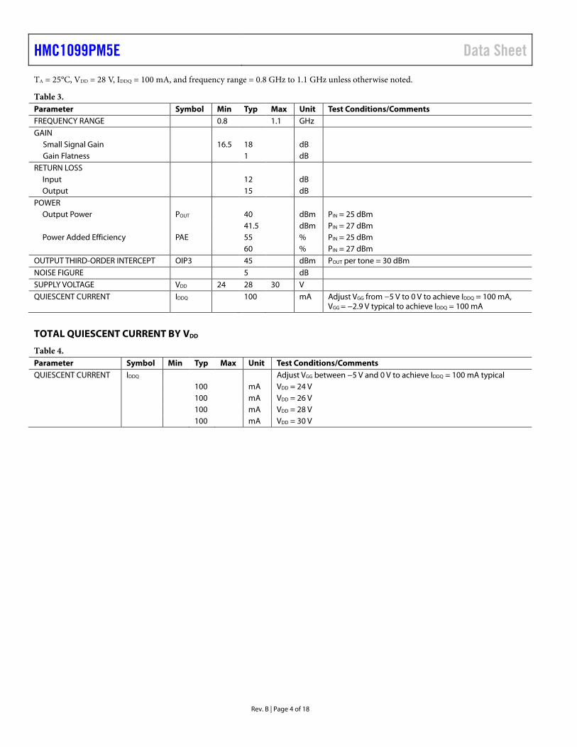
TA = 25°C, VDD = 28 V, IDDQ = 100 mA, and frequency range = 0.8 GHz to 1.1 GHz unless otherwise noted.
Table 3. Parameter Symbol Min Typ Max Unit Test Conditions/Comments FREQUENCY RANGE 0.8 1.1 GHz GAIN
Small Signal Gain 16.5 18 dB Gain Flatness 1 dB
RETURN LOSS Input 12 dB Output 15 dB
POWER Output Power POUT 40 dBm PIN = 25 dBm 41.5 dBm PIN = 27 dBm Power Added Efficiency PAE 55 % PIN = 25 dBm 60 % PIN = 27 dBm
OUTPUT THIRD-ORDER INTERCEPT OIP3 45 dBm POUT per tone = 30 dBm NOISE FIGURE 5 dB SUPPLY VOLTAGE VDD 24 28 30 V QUIESCENT CURRENT IDDQ 100 mA Adjust VGG from −5 V to 0 V to achieve IDDQ = 100 mA,
VGG = −2.9 V typical to achieve IDDQ = 100 mA
TOTAL QUIESCENT CURRENT BY VDD
Table 4. Parameter Symbol Min Typ Max Unit Test Conditions/Comments QUIESCENT CURRENT IDDQ Adjust VGG between −5 V and 0 V to achieve IDDQ = 100 mA typical
100 mA VDD = 24 V 100 mA VDD = 26 V 100 mA VDD = 28 V 100 mA VDD = 30 V

Data Sheet HMC1099PM5E
Rev. B | Page 5 of 18
ABSOLUTE MAXIMUM RATINGS Table 5. Parameter1 Rating Supply Voltage (VDD) 32 V Gate Bias Voltage (VGG) −8 V to 0 V Radio Frequency Input Power (RFIN) 33 dBm Voltage Standing Wave Ratio (VSWR)2 6:1 Channel Temperature 225°C Peak Reflow Temperature Moisture
Sensitivity Level 3 (MSL3)3 260°C
Continuous Power Dissipation, PDISS (TA = 85°C, Derate 151.5 mW/°C Above 85°C)
21.21 W
Storage Temperature Range −65°C to +150°C Operating Temperature Range −40°C to +85°C Electrostatic Discharge (ESD) Sensitivity
Human Body Model Class 1B, passed 500 V
1 When referring to a single function of a multifunction pin in the parameters, only the portion of the pin name that is relevant to the absolute maximum rating is listed. For full pin names of multifunction pins, refer to the Pin Configuration and Function Descriptions section.
2 Restricted by maximum power dissipation. 3 See the Ordering Guide for additional information.
Stresses at or above those listed under Absolute Maximum Ratings may cause permanent damage to the product. This is a stress rating only; functional operation of the product at these or any other conditions above those indicated in the operational section of this specification is not implied. Operation beyond the maximum operating conditions for extended periods may affect product reliability.
THERMAL RESISTANCE Thermal performance is directly linked to printed circuit board (PCB) design and operating environment. Careful attention to PCB thermal design is required.
θJC is the junction to case thermal resistance.
Table 6. Thermal Resistance Package Type θJC Unit CG-32-21 6.6 °C/W
1 Thermal resistance (θJC) was determined by simulation under the following conditions: the heat transfer is due solely to thermal conduction from the channel, through the ground paddle, to the PCB, and the ground paddle is held constant at the operating temperature of 85°C.
ESD CAUTION

HMC1099PM5E Data Sheet
Rev. B | Page 6 of 18
PIN CONFIGURATION AND FUNCTION DESCRIPTIONS
GNDNICNIC
RFIN/VGGRFIN/VGG
NICNIC
GND GNDNICNICRFOUT/VDD
RFOUT/VDD
NICNICGND
GN
D
NIC
NIC
NIC
NIC
NIC
NIC
GN
DG
ND
NIC
NIC
NIC
NIC
NIC
NIC
GN
D
HMC1099PM5ETOP VIEW
(Not to Scale)
NOTES1. EXPOSED PAD. THE EXPOSED PAD MUST BE CONNECTED TO RF AND DC GROUND.2. NO INTERNAL CONNECTION. THESE PINS ARE NOT CONNECTED INTERNALLY. HOWEVER, ALL DATA WAS MEASURED WITH THESE PINS CONNECTED TO RF AND DC GROUND EXTERNALLY.
17
1
34
2
9
5678
18192021222324
121110 13 14 15 162526272829303132
1682
6-00
2
Figure 2. Pin Configuration
Table 7. Pin Function Descriptions Pin No. Mnemonic Description 1, 8, 9, 16, 17, 24, 25, 32 GND Ground. These pins must be connected to RF and dc ground. See Figure 3 for the GND interface
schematic. 2, 3, 6, 7, 10 to 15, 18,
19, 22, 23, 26 to 31 NIC No Internal Connection. These pins are not connected internally. However, all data was measured
with these pins connected to RF and dc ground externally. 4, 5 RFIN/VGG RF Input/Gate Bias Control Voltage. This pin is a multifunction pin. The RFIN/VGG pin is dc-coupled
with internal prematching and requires external matching to 50 Ω, as shown in Figure 49. See Figure 4 for the RFIN/VGG interface schematic.
20, 21 RFOUT/VDD RF Output/Supply Voltage. This pin is a multifunction pin. The RFOUT/VDD pin is dc-coupled and requires external matching to 50 Ω, as shown in Figure 49. See Figure 4 for the RFOUT/VDD interface schematic.
EPAD Exposed Pad. The exposed pad must be connected to RF and dc ground.
INTERFACE SCHEMATICS
GND
1682
6-00
3
Figure 3. GND Interface
RFOUT/VDD
RFIN/VGG
1682
6-00
4
Figure 4. RFIN/VGG and RFOUT/VDD Interface

Data Sheet HMC1099PM5E
Rev. B | Page 7 of 18
TYPICAL PERFORMANCE CHARACTERISTICS 25
20
15
05
10
–5
0
–15
–10
–200 1.4
RES
PON
SE (d
B)
FREQUENCY (GHz)
INPUT RETURN LOSSOUTPUT RETURN LOSSGAIN
0.2 0.4 0.6 0.8 1.0 1.2
1682
6-00
5
Figure 5. Response vs. Frequency, Broadband Gain and Return Loss
25
5
GA
IN (d
B)
7
9
11
13
15
17
19
21
23
0FREQUENCY (GHz)
0.2 0.4 0.6 0.8 1.0 1.2
30V28V26V24V
1682
6-00
6
Figure 6. Gain vs. Frequency at Various Supply Voltages
0 0.2 0.4 0.6 0.8 1.0 1.2
0
–5
–15
–10
–20
–25
INPU
T R
ETU
RN
LO
SS (d
B)
FREQUENCY (GHz)
+85°C+25°C–40°C
1682
6-00
7
Figure 7. Input Return Loss vs. Frequency at Various Temperatures
0 0.2 0.4 0.6 0.8 1.0 1.2
25
5
GA
IN (d
B)
7
9
11
13
15
17
19
21
23
FREQUENCY (GHz)
+85°C+25°C–40°C
1682
6-00
8
Figure 8. Gain vs. Frequency at Various Temperatures
0 0.2 0.4 0.6 0.8 1.0 1.2
25
5
GA
IN (d
B)
7
9
11
13
15
17
19
21
23
FREQUENCY (GHz)
50mA100mA150mA200mA250mA
1682
6-00
9
Figure 9. Gain vs. Frequency at Various Quiescent Currents
0 0.2 0.4 0.6 0.8 1.0 1.2
0
–5
–15
–10
–20
–25
INPU
T R
ETU
RN
LO
SS (d
B)
FREQUENCY (GHz)
30V28V26V24V
1682
6-01
0
Figure 10. Input Return Loss vs. Frequency at Various Supply Voltages

HMC1099PM5E Data Sheet
Rev. B | Page 8 of 18
0 0.2 0.4 0.6 0.8 1.0 1.2
0
–5
–15
–10
–20
–25
INPU
T R
ETU
RN
LO
SS (d
B)
FREQUENCY (GHz)
50mA100mA150mA200mA250mA
1682
6-01
1
Figure 11. Input Return Loss vs. Frequency at Various Quiescent Currents
0 0.2 0.4 0.6 0.8 1.0 1.2
0
–5
–15
–10
–20
–25
OU
TPU
T R
ETU
RN
LO
SS (d
B)
FREQUENCY (GHz)
30V28V26V24V
1682
6-01
2
Figure 12. Output Return Loss vs. Frequency at Various Supply Voltages
44
300 1.2
OU
TPU
T PO
WER
(dB
m)
32
34
36
38
40
42
0.2 0.4 0.6 0.8 1.0FREQUENCY (GHz)
+85°C+25°C–40°C
1682
6-01
3
Figure 13. Output Power vs. Frequency at Various Temperatures,
PIN = 25 dBm
0 0.2 0.4 0.6 0.8 1.0 1.2
0
–5
–15
–10
–20
–25
OU
TPU
T R
ETU
RN
LO
SS (d
B)
FREQUENCY (GHz)
+85°C+25°C–40°C
1682
6-01
4
Figure 14. Output Return Loss vs. Frequency at Various Temperatures
0 0.2 0.4 0.6 0.8 1.0 1.2
0
–5
–15
–10
–20
–25
OU
TPU
T R
ETU
RN
LO
SS (d
B)
FREQUENCY (GHz)
50mA100mA150mA200mA250mA
1682
6-01
5
Figure 15. Output Return Loss vs. Frequency at Various Quiescent Currents
44
300 1.2
OU
TPU
T PO
WER
(dB
m)
32
34
36
38
40
42
0.2 0.4 0.6 0.8 1.0FREQUENCY (GHz)
30V28V26V24V
1682
6-01
6
Figure 16. Output Power vs. Frequency at Various Supply Voltages,
PIN = 25 dBm

Data Sheet HMC1099PM5E
Rev. B | Page 9 of 18
44
300 1.2
OU
TPU
T PO
WER
(dB
m)
32
34
36
38
40
42
0.2 0.4 0.6 0.8 1.0FREQUENCY (GHz)
50mA100mA150mA200mA250mA
1682
6-01
7
Figure 17. Output Power vs. Frequency at Various Quiescent Currents,
PIN = 25 dBm
44
300 1.2
OU
TPU
T PO
WER
(dB
m)
32
34
36
38
40
42
0.2 0.4 0.6 0.8 1.0FREQUENCY (GHz)
30V28V26V24V
1682
6-01
8
Figure 18. Output Power vs. Frequency at Various Supply Voltages,
PIN = 27 dBm
80
0
PAE
(%)
FREQUENCY (GHz)
10
20
30
40
50
60
70
0 1.20.2 0.4 0.6 0.8 1.0FREQUENCY (GHz)
+85°C+25°C–40°C
1682
6-01
9
Figure 19. PAE vs. Frequency at Various Temperatures, PIN = 25 dBm
44
300 1.2
OU
TPU
T PO
WER
(dB
m)
32
34
36
38
40
42
0.2 0.4 0.6 0.8 1.0FREQUENCY (GHz)
+85°C+25°C–40°C
1682
6-02
0
Figure 20. Output Power vs. Frequency at Various Temperatures,
PIN = 27 dBm
44
300 1.2
OU
TPU
T PO
WER
(dB
m)
32
34
36
38
40
42
0.2 0.4 0.6 0.8 1.0FREQUENCY (GHz)
50mA100mA150mA200mA250mA
1682
6-02
1
Figure 21. Output Power vs. Frequency at Various Quiescent Currents,
PIN = 27 dBm
80
0
PAE
(%)
FREQUENCY (GHz)
10
20
30
40
50
60
70
0 1.20.2 0.4 0.6 0.8 1.0FREQUENCY (GHz)
+85°C+25°C–40°C
1682
6-02
2
Figure 22. PAE vs. Frequency at Various Temperatures,
PIN = 27 dBm

HMC1099PM5E Data Sheet
Rev. B | Page 10 of 18
48
20
OU
TPU
T PO
WER
(dB
m)
24
28
32
36
40
44
FREQUENCY (GHz)0 1.20.2 0.4 0.6 0.8 1.0
FREQUENCY (GHz)
15dBm17dBm19dBm21dBm23dBm25dBm27dBm30dBm
1682
6-02
3
Figure 23. Output Power vs. Frequency at Various Input Powers
1200
0
SUPP
LY C
UR
REN
T (m
A)
200
400
600
800
1000
FREQUENCY (GHz)0 1.20.2 0.4 0.6 0.8 1.0
FREQUENCY (GHz)
15dBm17dBm19dBm21dBm23dBm25dBm27dBm30dBm
1682
6-02
4
Figure 24. Supply Current (IDD) vs. Frequency at Various Input Powers
60
30
OIP
3 (d
Bm
)
35
40
45
50
55
FREQUENCY (GHz)0 1.20.2 0.4 0.6 0.8 1.0
FREQUENCY (GHz)
30V28V26V24V
1682
6-02
5
Figure 25. OIP3 vs. Frequency at Various Supply Voltages,
POUT per Tone = 30 dBm
90
0
PAE
(%)
10
20
30
40
50
60
70
80
FREQUENCY (GHz)0 1.20.2 0.4 0.6 0.8 1.0
FREQUENCY (GHz)
15dBm17dBm19dBm21dBm
23dBm25dBm27dBm30dBm
1682
6-02
6
Figure 26. PAE vs. Frequency at Various Input Powers
60
30
OIP
3 (d
Bm
)
35
40
45
50
55
FREQUENCY (GHz)0 1.20.2 0.4 0.6 0.8 1.0
FREQUENCY (GHz)
+85°C+25°C–40°C
1682
6-02
7
Figure 27. OIP3 vs. Frequency at Various Temperatures,
POUT per Tone = 30 dBm
60
30
OIP
3 (d
Bm
)
35
40
45
50
55
FREQUENCY (GHz)0 1.20.2 0.4 0.6 0.8 1.0
FREQUENCY (GHz)
50mA100mA150mA200mA250mA
1682
6-02
8
Figure 28. OIP3 vs. Frequency at Various Quiescent Currents,
POUT per Tone = 30 dBm

Data Sheet HMC1099PM5E
Rev. B | Page 11 of 18
60
20
OIP
3 (d
Bm
)
25
30
35
40
45
50
55
FREQUENCY (GHz)0 1.20.2 0.4 0.6 0.8 1.0
FREQUENCY (GHz)
20dBm22dBm24dBm26dBm28dBm30dBm32dBm
1682
6-02
9
Figure 29. OIP3 vs. Frequency at Various POUT per Tone
65
2010 32
IMD
3 (d
Bc)
POUT PER TONE (dBm)
25
30
35
40
45
50
55
60
12 14 16 18 20 22 24 26 28 30
0.02GHz0.1GHz0.4GHz1.0GHz1.1GHz
1682
6-03
0
Figure 30. Output Third-Order Intermodulation (IMD3) vs. POUT per Tone,
VDD = 26 V
65
2010 32
IMD
3 (d
Bc)
POUT PER TONE (dBm)
25
30
35
40
45
50
55
60
12 14 16 18 20 22 24 26 28 30
0.02GHz0.1GHz0.4GHz1.0GHz1.1GHz
1682
6-03
1
Figure 31. IMD3 vs. POUT per Tone,
VDD = 30 V
65
2010 32
IMD
3 (d
Bc)
POUT PER TONE (dBm)
25
30
35
40
45
50
55
60
12 14 16 18 20 22 24 26 28 30
0.02GHz0.1GHz0.4GHz1.0GHz1.1GHz
1682
6-03
2
Figure 32. IMD3 vs. POUT per Tone,
VDD = 24 V
65
2010 32
IMD
3 (d
Bc)
POUT PER TONE (dBm)
25
30
35
40
45
50
55
60
12 14 16 18 20 22 24 26 28 30
0.02GHz0.1GHz0.4GHz1.0GHz1.1GHz
1682
6-03
3
Figure 33. IMD3 vs. POUT per Tone,
VDD = 28 V
90
00 30
OU
TPU
T PO
WER
(dB
m),
GA
IN (d
B),
PAE
(%)
INPUT POWER (dBm)
10
20
30
40
50
60
70
80
2 4 6 8 10 12 14 16 18 20 22 24 26 28
POUTGAINPAEIDD
900
0
I DD
(mA
)
100
200
300
400
600
500
700
800
1682
6-03
4
Figure 34. Output Power, Gain, PAE, and IDD vs. Input Power at 0.02 GHz

HMC1099PM5E Data Sheet
Rev. B | Page 12 of 18
70
0
840
0
I DD
(mA
)
120
240
360
480
600
720
OU
TPU
T PO
WER
(dB
m),
GA
IN (d
B),
PAE
(%)
10
20
30
40
50
60
0 30INPUT POWER (dBm)
2 4 6 8 10 12 14 16 18 20 22 24 26 28
POUTGAINPAEIDD
1682
6-03
5
Figure 35. Output Power, Gain, PAE, and IDD vs. Input Power at 0.1 GHz
0 30INPUT POWER (dBm)
2 4 6 8 10 12 14 16 18 20 22 24 26 28
I DD
(mA
)
OU
TPU
T PO
WER
(dB
m),
GA
IN (d
B),
PAE
(%)
10
20
30
40
50
60
70
80
0
75
150
225
300
375
450
525
600
0
1682
6-03
6
POUTGAINPAEIDD
Figure 36. Output Power, Gain, PAE, and IDD vs. Input Power at 1.1 GHz
35
00 1.2
SEC
ON
D H
AR
MO
NIC
(dB
c)
FREQUENCY (GHz)
5
10
15
20
25
30
0.2 0.4 0.6 0.8 1.0
30V28V26V24V
1682
6-03
7
Figure 37. Second Harmonic vs. Frequency at Various Supply Voltages,
PIN = 15 dBm
0 30INPUT POWER (dBm)
2 4 6 8 10 12 14 16 18 20 22 24 26 28
OUTPUT POWERGAINPAEIDD
OU
TPU
T PO
WER
(dB
m),
GA
IN (d
B),
PAE
(%)
10
20
30
40
50
60
70
80
0
800
0
I DD
(mA
)
100
200
300
400
500
600
700
1682
6-03
8
Figure 38. Output Power, Gain, PAE, and IDD vs. Input Power at 0.4 GHz
35
00 1.2
SEC
ON
D H
AR
MO
NIC
(dB
c)
FREQUENCY (GHz)
5
10
15
20
25
30
0.2 0.4 0.6 0.8 1.0
+85°C+25°C–40°C
1682
6-03
9
Figure 39. Second Harmonic vs. Frequency at Various Temperatures, PIN = 15 dBm
35
00 1.2
SEC
ON
D H
AR
MO
NIC
(dB
c)
FREQUENCY (GHz)
5
10
15
20
25
30
0.2 0.4 0.6 0.8 1.0
50mA100mA150mA200mA250mA
1682
6-04
0
Figure 40. Second Harmonic vs. Frequency at Various Quiescent Currents,
PIN = 15 dBm

Data Sheet HMC1099PM5E
Rev. B | Page 13 of 18
35
00 1.2
SEC
ON
D H
AR
MO
NIC
(dB
c)
FREQUENCY (GHz)
5
10
15
20
25
30
0.2 0.4 0.6 0.8 1.0
15dBm17dBm19dBm21dBm23dBm25dBm27dBm30dBm
1682
6-04
1
Figure 41. Second Harmonic vs. Frequency at Various Input Powers
12
0
NO
ISE
FIG
UR
E (d
B)
2
4
6
8
10
FREQUENCY (GHz)0 1.20.2 0.4 0.6 0.8 1.0
FREQUENCY (GHz)
+85°C+25°C–40°C
1682
6-04
2
Figure 42. Noise Figure vs. Frequency at Various Temperatures
12
0
NO
ISE
FIG
UR
E (d
B)
2
4
6
8
10
FREQUENCY (GHz)0 1.20.2 0.4 0.6 0.8 1.0
FREQUENCY (GHz)
30V28V26V24V
1682
6-04
3
Figure 43. Noise Figure vs. Frequency at Various Supply Voltages
0
–70
REV
ERSE
ISO
LATI
ON
(dB
)
–60
–50
–40
–30
–20
–10
0 1.20.2 0.4 0.6 0.8 1.0FREQUENCY (GHz)
+85°C+25°C–40°C
1682
6-04
4
Figure 44. Reverse Isolation vs. Frequency at Various Temperatures
24
0
4
12
20
8
16
0 20 40 60 80 100
NO
ISE
FIG
UR
E (d
B)
FREQUENCY (MHz)
+85°C+25°C–40°C
1682
6-04
5
Figure 45. Noise Figure vs. Frequency at Various Temperatures,
Low Frequency
12
0
NO
ISE
FIG
UR
E (d
B)
2
4
6
8
10
FREQUENCY (GHz)0 1.20.2 0.4 0.6 0.8 1.0
FREQUENCY (GHz)
50mA100mA150mA200mA250mA
1682
6-04
6
Figure 46. Noise Figure vs. Frequency at Various Quiescent Currents

HMC1099PM5E Data Sheet
Rev. B | Page 14 of 18
24
22
12
14
16
18
20
10
8
6
4
2
00 105 15 20 25 30
POW
ER D
ISSI
PATI
ON
(W)
INPUT POWER (dBm)
0.01GHz0.1GHz0.4GHz0.8GHz1.1GHzMAXIMUM PDISS AT 85°C
1682
6-04
7
Figure 47. Power Dissipation vs. Input Power at Various Frequencies,
TA = 85°C
300
–50–3.5 –2.7
I DD
(mA
)
VGG (V)
0
50
100
150
200
250
–3.4 –3.3 –3.2 –3.1 –3.0 –2.9 –2.8
1682
6-04
8
Figure 48. IDD vs. VGG at VDD = 28 V, Representative of a Typical Device

Data Sheet HMC1099PM5E
Rev. B | Page 15 of 18
THEORY OF OPERATION The HMC1099PM5E is a 10 W (40 dBm), gallium nitride (GaN), power amplifier that consists of a single gain stage that effectively operates like a single field effect transistor (FET). The device is internally prematched so that a simple, external matching network optimizes the performance across the entire
operating frequency range. The recommended dc bias conditions put the device in Class AB operation, resulting in high output power (41.5 dBm typical at PIN = 27 dBm) at improved levels of power efficiency (60% typical at PIN = 27 dBm).

HMC1099PM5E Data Sheet
Rev. B | Page 16 of 18
APPLICATIONS INFORMATION The supply voltage is applied through the RFOUT/VDD pin, and the gate bias voltage is applied through the RFIN/VGG pin. For operation of a single application circuit across the entire frequency range, it is recommended to use the external matching components specified in the typical application circuit (L1, C1, L3, and C8) shown in Figure 49. If operation is only required across a narrower frequency range, performance may be optimized additionally through the implementation of alternate matching networks. Capacitive bypassing of VDD and VGG is recommended.
The recommended power-up bias sequence follows:
1. Connect the power supply ground to the circuit ground. 2. Set VGG to −8 V to pinch off the drain current. 3. Set VDD to 28 V to pinch off the drain current. 4. Adjust VGG between −3 V and −2.5 V until a quiescent
current of IDDQ = 100 mA is obtained. 5. Apply the RF signal.
The recommended power-down bias sequence follows:
1. Turn off the RF signal. 2. Set VGG to −8 V to pinch off the drain current. 3. Set VDD to 0 V. 4. Set VGG to 0 V.
All measurements for this device were taken using the typical application circuit, configured as shown in the typical application circuit (see Figure 49). The bias conditions shown in the electrical specifications table (see Table 1 to Table 3) are the recommended operating points to optimize the overall performance. Unless otherwise noted, the data shown was taken using the recommended bias conditions. Operation of the HMC1099PM5E under other bias conditions may provide performance that differs from what is shown in the Typical Performance Characteristics section.
The evaluation PCB provides the HMC1099PM5E in its typical application circuit, allowing easy operation using standard dc power supplies and 50 Ω RF test equipment.
1
2
3
4
5
6
7
8
32 31 30 29 28 27 26 25
9 10 11 12 13 14 15 16
17
18
19
20
21
22
23
24
C22200pF
RFINL3
5.6nHL1
5.4nH
R168.1Ω
C42200pF
C710µF
C610µF
VDDVGG
C83.3pF
C910µF
C1010µF
C52200pF
L20.9µH
C13.3pF
C32200pF
RFOUT
1682
6-04
9
HMC1099PM5E
Figure 49. Typical Application Circuit

Data Sheet HMC1099PM5E
Rev. B | Page 17 of 18
EVALUATION PCB Use RF circuit design techniques for the PCB used in the device. Provide a 50 Ω impedance for the signal lines and directly connect the package ground leads and exposed pad to the ground plane, similar to that shown in Figure 50. Use a
sufficient number of via holes to connect the top and bottom ground planes. The evaluation circuit board shown in Figure 50 is available from Analog Devices, Inc., upon request.
1682
6-05
0
Figure 50. Evaluation PCB
Table 8. Bill of Materials for Evaluation PCB EV1HMC1099PM5 Item Description J1 DC pin J2, J3 SMA connectors, 25-146-1000-92 J4 Preform jumper C1, C8 3.3 pF capacitors, 0603 package C2 to C5 2200 pF capacitors, 0603 package C6, C7, C9, C10 10 µF capacitors, 1210 package L1 5.4 nH inductor, 0906 package L2 0.9 µH inductor, 1008 package L3 5.6 nH inductor, 0402 package R1 68.1 Ω resistor, 0603 package U1 HMC1099PM5E amplifier Heat Sink Used for thermal transfer from the HMC1099PM5E amplifier PCB EV1HMC1099PM5 PCB, circuit board material: Rogers 4350 or Arlon 25FR

HMC1099PM5E Data Sheet
Rev. B | Page 18 of 18
OUTLINE DIMENSIONS
08-1
5-20
18-A
1
0.50BSC
BOTTOM VIEWTOP VIEW
SIDE VIEW
PIN 1INDICATOR
32
916
17
24
25
8
0.300.250.20
5.105.00 SQ4.90
FOR PROPER CONNECTION OFTHE EXPOSED PAD, REFER TOTHE PIN CONFIGURATION ANDFUNCTION DESCRIPTIONSSECTION OF THIS DATA SHEET.
0.450.400.35
3.203.10 SQ3.00
PKG
-005
068
3.50 REF
EXPOSEDPAD
1.351.251.15 0.050 MAX
0.035 NOM
0.203 REF
0.400.60 REF
COPLANARITY0.08SEATING
PLANE
PIN 1INDICATOR AREA OPTIONS(SEE DETAIL A)
DETAIL A(JEDEC 95)
Figure 51. 32-Lead Lead Frame Chip Scale Package, Premolded Cavity [LFCSP_CAV]
5 mm × 5 mm Body and 1.25 mm Package Height (CG-32-2)
Dimensions shown in millimeters
ORDERING GUIDE
Model1, 2 Temperature Range
MSL Rating3 Description4
Package Option
HMC1099PM5E −40°C to +85°C MSL3 32-Lead Lead Frame Chip Scale Package, Premolded Cavity [LFCSP_CAV] CG-32-2 HMC1099PM5ETR −40°C to +85°C MSL3 32-Lead Lead Frame Chip Scale Package, Premolded Cavity [LFCSP_CAV] CG-32-2 EV1HMC1099PM5 Evaluation Board 1 All models are RoHS compliant. 2 When ordering the evaluation board only, reference the model number, EV1HMC1099PM5. 3 See the Absolute Maximum Ratings section for additional information. 4 The lead finish of the HMC1099PM5E and the HMC1099PM5ETR are nickel palladium gold (NiPdAu).
©2018 Analog Devices, Inc. All rights reserved. Trademarks and registered trademarks are the property of their respective owners. D16826-0-9/18(B)