high power x-band rf test stand development and ... - cern
TRANSCRIPT

High Power X-band RF Test Stand
Development and High Power
Testing of the CLIC Crab Cavity
Benjamin J. Woolley
This thesis is submitted in partial fulfilment of the
requirements
for the degree of Doctor of Philosophy
August 2015


i
Abstract
This thesis describes the development and operation of multiple high power X-band
RF test facilities for high gradient acceleration and deflecting structures at CERN, as re-
quired for the e+ e- collider research programme CLIC (Compact Linear Collider). Signif-
icant improvements to the control system and operation of the first test stand, Xbox-1
are implemented. The development of the second X-band test stand at CERN, Xbox-2 is
followed from inception to completion. The LLRF (Low Level Radio Frequency) system,
interlock system and control algorithms are designed and validated. The third test stand
at CERN, Xbox-3 is introduced and designs for the LLRF and control systems are pre-
sented. The first of the modulator/klystron units from Toshiba and Scandinova is tested.
CLIC will require crab cavities to align the bunches in order to provide effective head-
on collisions. An X-band travelling wave cavity using a quasi-TM11 mode for deflection
has been designed, manufactured and tested at the Xbox-2 high power test stand. The
cavity reached an input power level in excess of 50 MW, at pulse widths of 150 ns with a
measured breakdown rate (BDR) of better than 10 -5 breakdowns per pulse (BDs/pulse).
At the nominal pulse width of 200 ns, the cavity reached an input power level of 43 MW
with a BDR of 10-6 BDs/pulse. These parameters are well above the nominal design pa-
rameters of an input power of 13.35 MW with a 200 ns pulse length. This work also de-
scribes surface field quantities which are important in assessing the expected BDR when
designing high gradient structures.
ii
Acknowledgements
I would like to thank Amos Dexter for his supervision and for giving me the oppo r-
tunity to partake in this PhD. I would also like to thank those others at Lancaster Uni-
versity who have provided guidance including Graeme Burt, Praveen Ambattu and
Shokrollah Karimian. In particular to Graeme and Praveen, who designed such an inter-
esting cavity forming the basis of much of the work presented in this thesis.
My special thanks go to Igor Syratchev for his supervision during my time at CERN.
His guidance and ideas always left me with many new avenues of research to pursue and
much to ponder about!
Thanks also to Walter Wuensch and Alexej Grudiev, whose stimulating conversations
led to the development of many of the ideas presented here. Thanks to Jan Kovermann
for his teaching on the operation of Xbox-1 and his ‘handing of the baton’ to me to be-
come the new Xbox control system designer and operator at CERN.
Also thanks to everyone who helped to make operating and designing the test stands
possible including Gerard McMonagle, Alberto Degiovanni, Nuria Catalan Lasheras, Stef-
fen Doebert, Andrey Olyunin, Luis Navarro, Jorge Giner Navarro and Esa Paju.
Further thanks go to Joseph Tagg from National Instruments for his significant con-
tribution in the programming of the PXI hardware using his vast LabVIEW expertise. I
would also like to thank the LLRF experts at CERN: Stephane Rey, Luca Timeo, Heiko
Damerau and Alexandra Andersson for their discussions and help with LLRF system de-
signs.
Thanks also to Rolf Wegner for his expertise in tuning high gradient structures and in
particular his management in tuning the crab cavity. Thanks also to Wilfrid Farabolini
and Robin Rajamaki for their work on the breakdown cell location algorithms and results.
Thanks to Germana Riddone and Anastasia Solodko for overseeing structure production
and manufacturing and providing the test stands with devices to test. Thanks to Marek
Jacewicz and Roger Ruber for adding such an interesting experiment to the test stands;
the dark current spectrometer. Thanks to Valery Dolgashev, Sami Tantawi, Matt Franzi
and the ASTA team for being so hospitable during my short stay at SLAC.
I would also like to show my gratitude to STFC for granting me the scholarship and
LTA funding that has supported me for the past 4 years.
The research leading to these results has received funding from the European Com-
mission under the FP7 Research Infrastructures project EuCARD-2, grant agreement
no.312453.
Finally, I would like to thank my family for their support throughout, especially to
my girlfriend Eve Harrison whose patience and care has kept me content throughout my
time researching this PhD.

iii
Contents
Abstract .............................................................................................................. i
Acknowledgements ............................................................................................... i
List of Figures....................................................................................................vii
List of Tables .................................................................................................... xix
1 Introduction ................................................................................................1
1.1 Lepton colliders ........................................................................................1
1.2 CLIC.......................................................................................................2
1.3 Accelerator Technology Choice ..................................................................3
1.4 RF Breakdown .........................................................................................5
1.5 Fabrication of High Gradient Structures.....................................................5
1.6 RF Conditioning of High Gradient Structures .............................................6
1.7 Standalone X-band Test Stands .................................................................7
1.7.1 Test Stand layout ..............................................................................8
1.8 Crossing angle and Crab Cavities...............................................................8
1.9 Other Applications of high gradient X-band technology ...............................9
1.10 High phase stability ............................................................................ 10
1.11 Summary ........................................................................................... 10
Chapter 2 .......................................................................................................... 12
2 Xbox-1: CERN’s first 12 GHz standalone test stand...................................... 12
2.1 Reasons for standalone test stands ........................................................... 12
2.2 Test Stand Design: High Level RF ........................................................... 13
2.2.1 Klystron ......................................................................................... 14
2.2.2 Modulator ....................................................................................... 15
2.2.3 Pulse Compressor Operation with a 180º Phase Flip.......................... 15
2.2.4 Pulse Compressor Operation with a Phase Ramp ............................... 19
2.2.5 Pulse Compressor Cavity Design ....................................................... 22
2.2.6 Waveguide Network Components ...................................................... 23
2.3 Test Stand Design: LLRF and Diagnostics................................................ 25
2.3.1 Pulse forming network (PFN) ........................................................... 25

iv
2.3.2 RF signal acquisition ....................................................................... 26
2.4 Test Stand Performance ......................................................................... 27
2.4.1 Calibration of the RF acquisition system ........................................... 27
2.4.2 Pulse forming network (PFN) Upgrade ............................................. 30
2.4.3 Pulse Compressor Operation ............................................................ 32
2.4.4 Structure Conditioning Algorithm .................................................... 36
2.5 Conclusion ............................................................................................ 38
Chapter 3 .......................................................................................................... 40
3 Xbox-2 ..................................................................................................... 40
3.1 Increase of testing capacity ..................................................................... 40
3.2 Xbox-2 general layout ............................................................................ 40
3.2.1 Klystron/modulator ........................................................................ 41
3.2.2 Pulse Compressor and Waveguide components .................................. 42
3.2.3 Bunker and Device under Test ......................................................... 43
3.3 LLRF System Development .................................................................... 43
3.3.1 LLRF System Requirements............................................................. 43
3.3.2 LLRF System PXI Hardware ........................................................... 44
3.3.3 LLRF Up-conversion Hardware ........................................................ 45
3.3.4 LLRF Down-conversion Hardware .................................................... 47
3.3.5 LLRF system Tests ......................................................................... 48
3.3.6 RF Interlock Detection .................................................................... 56
3.3.7 RF Distribution and Layout............................................................. 58
3.4 New SLED-I Pulse Compressor ............................................................... 61
3.4.1 SLED-I RF design ........................................................................... 61
3.4.2 Pulse Compressor Tuning ................................................................ 62
3.4.3 Pulse Compressor Test .................................................................... 66
3.4.4 Pulse Flattening Algorithm .............................................................. 68
3.5 Waveguide Components ......................................................................... 70
3.5.1 Directional couplers ......................................................................... 70
3.5.2 RF Vacuum valves and Vacuum Ports .............................................. 71
3.6 PXI Timing, Interlocks and Control ........................................................ 72

v
3.6.1 FPGA Timing and Interlocks ........................................................... 72
3.6.2 Software Control and Interlocks ........................................................ 74
3.6.3 Timing and Interlocks Interface PCB ................................................ 74
3.6.4 Vacuum and Temperature Controls Rack .......................................... 76
3.6.5 Modulator Control System ............................................................... 78
3.7 Test stand Commissioning ...................................................................... 80
3.7.1 General User Interface ..................................................................... 80
3.7.2 Test Stand Hardware Checks............................................................ 85
3.7.3 RF Cable Calibration....................................................................... 86
3.7.4 First High Power RF ....................................................................... 87
3.7.5 Vacuum Feedback Algorithm............................................................ 88
3.7.6 RF Vacuum Valve Outgassing .......................................................... 90
3.7.7 Modulator Control Automation ........................................................ 93
3.8 Conclusion ............................................................................................. 94
Chapter 4 .......................................................................................................... 95
4 Xbox-3...................................................................................................... 95
4.1 Further Increase of Test Capacity with Reduced Cost ............................... 95
4.2 RF Combination Scheme......................................................................... 95
4.3 Klystron Factory Test Results ................................................................. 97
4.4 Laboratory Test of the 2-way Combination Scheme................................... 99
4.5 LLRF Hardware ................................................................................... 104
4.6 Racks and Layout ................................................................................ 107
4.7 Experimental Area Layout .................................................................... 110
4.8 CERN Site Acceptance Test of First Toshiba Klystron ............................ 112
4.9 RF Testing of the First Toshiba Klystron............................................... 114
4.9.1 Experiment Layout ........................................................................ 114
4.9.2 Control Software ........................................................................... 115
4.9.3 High Power Test ........................................................................... 121
4.10 Conclusion ....................................................................................... 126
Chapter 5 ........................................................................................................ 127
5 The CLIC Crab cavity ............................................................................. 127

vi
5.1 Crab Cavity Design...............................................................................127
5.1.1 Crab Cavity Requirements ..............................................................127
5.1.2 RF Cell Design ..............................................................................128
5.1.3 Structure Design ............................................................................130
5.2 Crab Cavity Fabrication........................................................................134
5.3 Structure Tuning ..................................................................................135
5.3.1 Tuning pins ...................................................................................135
5.3.2 Bead-pull apparatus .......................................................................136
5.3.3 Bead choice and field perturbations .................................................137
5.3.4 Bead-pull Method and Results.........................................................139
5.4 High Power Test...................................................................................144
5.4.1 Xbox-2 Bunker Layout and Diagnostics ...........................................144
5.4.2 Breakdown Detection .....................................................................145
5.4.3 Conditioning Process ......................................................................146
5.4.4 Conditioning Results ......................................................................146
5.4.5 Breakdown Cell Location ................................................................155
5.4.6 Breakdown Cell Migration ..............................................................159
5.5 Conclusion ...........................................................................................161
Chapter 6 .........................................................................................................162
6 Conclusions..............................................................................................162
6.1 High Power X-band test Stands at CERN...............................................162
6.1.1 Xbox-1 ..........................................................................................162
6.1.2 Xbox-2 ..........................................................................................162
6.1.3 Xbox-3 ..........................................................................................163
6.1.4 CLIC Crab Cavity Prototype ..........................................................163
6.2 Future Work ........................................................................................164
6.2.1 Xbox-3 Commissioning ...................................................................164
6.2.2 CLIC Crab Cavity Post Mortem Analysis ........................................164
Bibliography ............................................................................................166

vii
List of Figures
Figure 1.1: Schematic of the CLIC two beam system. RF power extracted from the drive
beam by the PETS is transferred to the main linac [12]. 3
Figure 1.2: The results of optimization are presented; the top left graph shows how the
FoM varies with frequency for several different accelerating gradients while the top right
graph shows the variation of the FoM as a function of accelerating gradient for several
different frequencies. The bottom graphs make the same comparisons but instead show
the total cost [16]. 4
Figure 1.3: Shows the processing history of a TD24R05 CLIC prototype structure tested
at KEK [25]. The red and green points show the accelerting gradient the pulse width
respectively. 6
Figure 1.4: Standalone test stand layout with optional second structure. 8
Figure 1.5: Interaction of two beams with and without crabbing. 9
Figure 2.1: Schematic of the high level RF layout of Xbox-1, with the associated LLRF
signals given in their abbreviated form. (See Table 3.8, p 86 for glossary of abbreviations).
13
Figure 2.2: Photos showing the layout of the Xbox-1 test stand. Clockwise from top left:
Scandinova modulator, Pulse compressor, bunker and high gradient structure under test.
14
Figure 2.3: Shows a simple schematic of a SLED I pulse compressor. 16
Figure 2.4: Shows the theoretical electric field (top) and power (bottom) profiles
obtainable using the Xbox-1 pulse compressor when a simple 180º flip is utilised. The
input pulses are shown in red and the ouput pulses in blue. 18
Figure 2.5: (Left) Shows the resulting mode pattern, absorber and vacuum port positions.
(Right) shows the mode production in the tapered mode converter as a fucntion of
propigation distance. 23
Figure 2.6: (Left) Shows the inner geometry and electric field of the mode launcher.
(Right) Photograph of the compact mode converter. 24

viii
Figure 2.7: Shows the RF vacuum valve electric field distribution and photograph of the
RF tapered sections. 24
Figure 2.8: Shows a schematic of the pulse forming network for Xbox-1. 25
Figure 2.9: Block diagram of the Xbox-1 control system. 27
Figure 2.10: Shows the typical method of calibration of the long RF cables used at Xbox-
1. 28
Figure 2.11: Gives an example of a permanent calibration setup built into the RF line. 29
Figure 2.12: Shows the "full chain" calibration procedure utilising a kW level TWT. 29
Figure 2.13: Shows the calibration of the IQ demodulator performed using the TWT
calibration method. The I and Q voltages are plotted on the complex plane (left) and the
measured angle shown (right). 30
Figure 2.14: Shows the mean flat-top power into the structure during a breakdown event
and the subsequent ramp back to full power. The 8-bit attenuator is used to control the
power level. 31
Figure 2.15: Shows the mean flat-top power into the structure during a structure
breakdown event and the subsequent ramp back to full power. The voltage tuned
attenuator with 16-bits of resolution is used, along with the new PID control. 31
Figure 2.16: Shows the mechanical drawing of the XBox-1 pulse compressor. 1. -3 dB
coupler. 2. TE10 to TE01 mode converter. 3 TE01 to TE01+TE02 tapered mode
converter with coupling iris. 4. Resonant cavities. 5. Pumping ports. 6. Piston tuners. 32
Figure 2.17: Shows the output power of the pulse compressor incident to the DUT (green)
and the external temperature of each pulse compressor cavity (red and blue). The RF
power interruption and subsequent cooling causes the pulse compressor to detune. 33
Figure 2.18: Shows typical, compressed output pulses, with an expanded view of the
minimum transmission point for different tuning regimes. 33
Figure 2.19: Shows a typical reflected pulse from the pulse compressor and the derivation
of the klystron reflection ratio. 34
Figure 2.20: Shows the power level out of the pulse compressor, the cavity temperatures
and the tuner's stepper motor positions after a cold start of the system. 35

ix
Figure 2.21: Shows the input power (green) and accumulated number of breakdowns
(black) in a T24 CLIC structure during conditioning at Xbox-1. Power was controlled by
the operator. 36
Figure 2.22: Shows the GUI for the Xbox-1 structure conditioning software. 37
Figure 2.23: Shows the power increase into a T24 CLIC prototype accelerating structure
as a function of the number of pulses (green). Also shown in red are the accumulated
number of breakdowns. 38
Figure 3.1: Shows a labelled, 3D drawing of the Xbox-2 test area, used in initial planning.
41
Figure 3.2: Shows the front side of the Xbox-2, Scandinova K3 modulator. 41
Figure 3.3: Shows a photograph of the XL5 klystron installed into the rear right hand
corner of the Xbox-2 modulator, as viewed from the perspective shown in Figure 3.2. 42
Figure 3.4: Shows the pulse compressor and surrounding waveguide components. 42
Figure 3.5: Shows the apparatus set up inside the bunker during commissioning. 43
Figure 3.6: Shows a simple schematic drawing of the NI PXIe-5673E RF vector signal
generator. 45
Figure 3.7: Shows the original, proposed RF generation scheme for Xbox-2. 46
Figure 3.8: Shows a schematic of the up conversion scheme used in Xbox-2. 47
Figure 3.9: Shows a schematic of the down mixing scheme employed at Xbox-2. 47
Figure 3.10: Shows the complete LLRF schematic and test setup created for Xbox-2. 48
Figure 3.11: Shows the signals acquired by the 5772 ADCs on the PXI crate. Left: raw
waveform of the reference signal. Right: raw waveform of the modulated signal. 49
Figure 3.12: A visual representation of the IQ software demodulation. 49
Figure 3.13: Left: Shows the power (amplitude squared) of the modulated pulse. Right:
Shows the phase of the modulated pulse. 50
Figure 3.14 shows the mechanical layout of the Xbox-2 LLRF system. 51

x
Figure 3.15: Shows the phase noise spectral density measured at 6 different locations. 53
Figure 3.16: Shows the phase and amplitude acquired by the LLRF and PXI system.
Various methods are used for the demodulation and are plotted in different colours. 55
Figure 3.17: Shows a schematic of the first amplification stage for the log detector system.
57
Figure 3.18: Shows the second stage of amplification for the log detector system. 57
Figure 3.19: Shows a schematic of the comparator circuit used for threshold detection. 58
Figure 3.20: Shows the directional couplers in-situ at the Xbox-2 bunker. 58
Figure 3.21: shows a schematic of the RF signal distribution inside the LLRF rack. 59
Figure 3.22: Shows a schematic of the power calibration method that will be used. 60
Figure 3.23: Shows a front and back view of the LLRF/controls rack at Xbox-2. 60
Figure 3.24: Shows the electric field pattern inside of the storage cavity of the new SLED
I [56]. 61
Figure 3.25: Shows the tuning piston and the mechanical action needed to increase or
reduce the frequency. 62
Figure 3.26: Shows the phase (top) and amplitude (bottom) of the return loss of each
cavity at different water temperatures. Cavity 1 is shown in blue and red for 30 and 40
degrees Celsius and cavity two is shown in green and purple for 19.2 and 30 degrees
Celsius. 63
Figure 3.27: Shows the reflection (blue) and transmission (red) coefficients of the pulse
compressor after the first machining operation. 64
Figure 3.28: Shows the transmission (S12) and reflection (S11) coefficients for the tuned
and detuned pulse compressor under vacuum. 64
Figure 3.29: Shows a simulated input pulse to the pulse compressor, in order to produce a
flat pulse with 250 ns pulse width. Power and phase are shown in black and red
respectively. 65

xi
Figure 3.30: Shows the simulated transmitted power (black) and phase (red) for the pulse
compressor with a 100 MW input pulse. 66
Figure 3.31: Shows the simulated reflected power (blue) and phase (green) for a 100 MW
input pulse. 66
Figure 3.32: Shows a photograph of the experimental setup used to test the pulse
compressor and LLRF system. 67
Figure 3.33: Shows the incident, transmitted and reflected pulses in red white and blue
respectively as measured by the PXI crate. The uncalibrated power is shown on the left
and the phase on the right. 67
Figure 3.34: Shows the calibrated power meters' readings of incident (yellow) and
transmitted (blue) power. The vertical scale is 500 W/div, while the horizontal scale is
200 ns/div. 68
Figure 3.35: Shows the power and phase of the incident and compressed pulses when
tuned using the pulse flattening algorithm. The incident power and phase are shown in
purple and blue respectively and the compressed power and phase are shown in red and
green respectively. 69
Figure 3.36: Shows the electric field profile (left) and a photograph (right) of the new
high power, -60 dB directional couplers. 70
Figure 3.37: Shows the electric field pattern inside the RF choke. 71
Figure 3.38: Shows the 3D drawings of the vacuum gate valve (left) and the vacuum port
(right). 72
Figure 3.39: Shows a photograph of the PXI crate populated with the cards needed to run
the test stand. 73
Figure 3.40: A Schematic diagram of the trigger and interlock board inputs and outputs.
75
Figure 3.41: Shows a photograph of the completed timing and interlock interface crate. 76
Figure 3.42: Shows a photograph of the vacuum and temperature controls rack at Xbox-2.
77

xii
Figure 3.43: Shows the Xbox-2 main operation window with annotations. See Table 3.8
on page 87, for the glossary of signal names. 81
Figure 3.44: Shows the trigger (left) and interlock (right) windows. 81
Figure 3.45: Shows the RF control window interface. 1. RF pulse settings. 2. Power
feedback loop settings. 3. BDR automatic power level conditioner settings. 4.
Conditioning mode select and settings. 5. Pulse phase settings. 82
Figure 3.46: Shows the acquisition settings general user interface. 83
Figure 3.47: Shows the display configurator's general user interface. 84
Figure 3.48: Shows a chart created to display the temperatures of the system. 84
Figure 3.49: Shows the breakdown settings window after a breakdown event has occurred.
The breakdown flags are shown on the left, the pulse shapes are shown in the graph with
the key on the right. See Table 3.8 on page 87, for the glossary of signal names. 85
Figure 3.50 shows the power meter display of the initial RF pulse produced by Xbox-2. 88
Figure 3.51: (Top) shows the average power level of the flat top of the klystron output
pulse (blue) and the compressed pulse before and after the dummy waveguide(red and
green). The bottom figure shows the pressure levels in the waveguide several different
locations with the vacuum feedback loop activated. 90
Figure 3.52: Shows the pressure inside different parts of the RF network. 91
Figure 3.53: Shows the klystron output (blue), DUT input (green) DUT output (yellow)
and DUT reflected (violet) pulses. 91
Figure 3.54: Shows photographs of each side of the RF flange and the comparison with
the simulated electric field pattern in HFSS [60]. 92
Figure 3.55: Shows the conditioning history of the waveguide system before and after the
RF vacuum valves had been removed. The orange green and red points show the power
levels at the klystron output, structure input and structure output respectively. The pulse
width is shown in purple and the accumulated number of interlocks in blue. 93
Figure 4.1: Shows different phase mapping between 4 klystrons (left) and the resulting 3D
simulation (right) for 4 different phase maps. Power can be combined into 4 different
testing slots by changing the relative phase between each klystron [61]. 96

xiii
Figure 4.2: Shows the high power RF network layout of Xbox-3 [62]. 97
Figure 4.3: Shows the gain curves (left) and power and efficiency Vs voltage curves
(right) for the Toshiba E37113 klystron [61]. 97
Figure 4.4: Shows the updated layout of Xbox-3 with the acquired channels indicated by
coloured arrows. The Faraday cup signals (orange), waveguide network reflected/interlock
signals (red), DUT signals (blue) and waveguide diagnostic/forward signals (green)
signals are shown. 98
Figure 4.5 shows a schematic drawing of the low power test conducted to test the 2 -way
combination scheme at Xbox-3. Coaxial components and connections are shown in blue,
waveguide components in orange/brown, LLRF mixing stages in black and PXI based
components in red. 99
Figure 4.6 shows the amplitude (blue solid and green dotted lines) and phase profiles (red
and purple lines) programmed into the RF generators in order to produce a 250 ns
compressed pulse. The phase profiles are produced by the recycled pulse flattening
algorithm. 101
Figure 4.7 shows the pulse shapes at the input to the pulse compressor (blue), the load
channel (red) and the transmitted power of the pulse compressor (green). 102
Figure 4.8 shows the amplitudes (solid lines) and phases (dashed lines) of two, 400 ns
compressed output pulses and the corresponding input pulses. One created using
amplitude modulated pulse (blue and green) and another using a phase modulated pulse
(red and purple). 103
Figure 4.9 shows the diode outputs on the oscilloscope. The vertical scale is 20 mV/div
for both traces. The horizontal scale is 0.5 ms/div. 103
Figure 4.10: Shows the mechanical drawing for the 1st shelf in the PLL crate. 104
Figure 4.11: Shows the mechanical layout for the second shelf in the PLL crate. 105
Figure 4.12: Shows a mechanical layout of the 1st shelf in one of the mixing crates. 106
Figure 4.13: Shows the mechanical layout of the 2nd shelf in one of the mixing crates. 106
Figure 4.14 shows a schematic drawing of the rack cooling circuit (left) and a photograph
of the empty rack (right). 108

xiv
Figure 4.15 shows the RF multiplexers and power meter used as part of the calibration
system at Xbox-3. The system shown is for one sub-system at Xbox-3. RF signals are
shown in blue, while Ethernet/control signals are red. 109
Figure 4.16 shows the rack layout for the Xbox-3 LLRF and control systems. Also shown
are the interconnects between each rack. Crate sizes are shown according to colour with
blue, grey, red and green being 1U, 2U, 3U and 4U respectively. 110
Figure 4.17 shows the layout of the modulators, waveguide combination network and
pulse compressors at Xbox-3. 111
Figure 4.18 shows the layout of the test slots inside the bunker in building 150. Support
structures for the waveguides are not shown to increase clarity. 111
Figure 4.19 shows a zoomed in view of test slot A and its associated waveguide
components. 112
Figure 4.20 shows the klystron cathode voltage and current in blue and red respectively,
as measured by the capacitive voltage divider and current transformer on the high voltage
side of the current transformer. 113
Figure 4.21 shows a schematic diagram of the high power RF network used to test the
first Xbox-3 klystron. The green arrows show signals that go to the LLRF system, while
red arrows show signals measured by a power meter. 114
Figure 4.22 shows the first klystron/modulator system in situ at building 150. 115
Figure 4.23 shows the operation of the NI 5793R RF transmitter. The RF transmitter
module hardware is shown in blue, the FPGA hardware in green and the backplane line
in red. 116
Figure 4.24 shows the 3 𝝁s pulse in the time (top) and frequency domains (bottom). 118
Figure 4.25 shows the sampled signal and its aliases (or images) in the first 4 Nyquist
zones. The -70 dB bandwidth of the signal in the top figure is 50 MHz, while for the
bottom figure it is 90 MHz. 119
Figure 4.26 shows the Nyquist zones for a 400 MHz signal acquired at a sample frequency
of 230 MHz. The -70 dB bandwidth of the signal is 90 MHz. 120

xv
Figure 4.27 shows a comparison between the 28 MHz (black) and 62 MHz (red) low pass
filters used after the demodulation. The time and frequency domains are shown in the top
and bottom figures respectively. 121
Figure 4.28 shows the first 77 hours of the klystron test. The klystron output power is
shown in red, the pulse width in blue and the accumulated number of interlocks in green.
122
Figure 4.29 shows the cathode voltage and current for a normal pulse (red and black) and
for an interlock pulse (blue and green). 123
Figure 4.30 shows the conditioning of the network from 77 hours of RF on time until the
end of the current run. 125
Figure 4.31 shows the klystron output and drive power for a peak pulse power of 7.5 MW.
125
Figure 5.1 shows the cell geometry and the E-field, H-field and the modified Poynting
vector ‘Sc’ [22] of the un-damped crab cavity as simulated in HFSS. 129
Figure 5.2 shows 3D models of a 5 cell crab cavity with the standard coupler (left) and
the waveguide coupler (right) [33]. 131
Figure 5.3 shows the full structure geometry with the electric fields (top), magnetic fields
(middle) and the modified Poynting vector (bottom) plotted on the surface for an input
power of 13.35 MW. The beam direction is from left to right, while the RF power flow is
from right to left. 132
Figure 5.4 illustrates how a travelling wave moves through an envelope in a slow wave
structure. 133
Figure 5.5 shows the magnitude of the deflecting components of the electric and magnetic
fields and the longitudinal component of the electric field. 134
Figure 5.6 shows a normal cell (left) and a coupling cell (right) after high presision
machining at VDL [79]. 135
Figure 5.7 shows a section of two cells with the tuning pins are incorporated. 136
Figure 5.8 shows the bead-pull apparatus in the CERN clean room. 136

xvi
Figure 5.9 shows the deflecting fields on axis and the long itudinal field at 1.5mm of
vertical displacement as simulated in HFSS. 138
Figure 5.10 shows the ∆𝑺𝟏𝟏 for a bead on axis and vertically offset by 0.8 mm and
1.2 mm [82]. The simulated length corresponds to 2.5 normal cells. 139
Figure 5.11 shows the S11 measurement taken during the first bead-pull. The real and
imaginary components are shown on the left and the phase shown on the right. The cells
are counted from the input coupler, with the bead pulled from right to left (i.e. from the
output coupler towards the input coupler) [83]. 140
Figure 5.12 Shows the crab cavity in position during the initial bead pull (left) and the
bent flange (right). The structure axis is shown in black and the offset axis is shown in
red. 140
Figure 5.13 shows the initial bead pull results. The magnitude of S11 is shown in the top
figure, the phase advance in the middle figure and the real and imaginary parts of S11 in
the bottom figure. 141
Figure 5.14 shows the bead pull results for the fully tuned CLIC crab cavity. The
magnitude of S11 is shown in the top figure, the phase advance in the middle figure and
the real and imaginary parts of S11 in the bottom figure. 143
Figure 5.15 shows a schematic layout of the crab cavity and the various diagnostic
systems. The red arrows show signals that are sent directly to the PXI crate for
acquisition and analysis. 144
Figure 5.16 shows the crab cavity inside the bunker with the surrounding diagnostics. 145
Figure 5.17 shows the generalised conditioning curve used to process high gradient
structures at CERN and KEK. Total conditioning time is usually around 2000 RF hours
i.e. 360 million pulses. 146
Figure 5.18 shows the input power level (red), accumulated number of breakdowns
(green), pulse width at half maximum (blue) and BDR (black) during the first 25 million
RF pulses of the crab cavity high power test. 147
Figure 5.19 shows the nominal operating parameter run at 14MW. The input power level
(red), accumulated number of breakdowns (green), pulse width at half maximum (blue)
and BDR (black) are plotted. 148

xvii
Figure 5.20 shows the conditioning curve from 18.5 MW up to 27 MW for a 100 ns flat-
top pulse width. The input power level (red), accumulated number of breakdowns (green),
pulse width at half maximum (blue) and BDR (black) are plotted. 149
Figure 5.21 shows the run at a power level of 20.3 MW and a flat top pulse width of
200 ns. The input power level (red), accumulated number of breakdowns (green), pulse
width at half maximum (blue) and BDR (black) are plotted. 150
Figure 5.22 shows the complete compressed pulse shape (left) and a comparison between
the compressed flat-top pulse and the pulse with the pulse compressor detuned (right).151
Figure 5.23 shows the high power test from 135 million pulses to 276 million pulses. The
input power level (red), accumulated number of breakdowns (green), pulse width at half
maximum (blue) and BDR (black) are plotted. 152
Figure 5.24 shows the data taken during the constant power run in which the pulse width
was varied. The input power level (red), accumulated number of breakdowns (green),
pulse width at half maximum (blue) and BDR (black) are plotted. 153
Figure 5.25 shows the FWHM pulse width versus breakdown rate dependency for the crab
cavity. 153
Figure 5.26 shows the run in which the power level was varied. The input power level
(red), accumulated number of breakdowns (green), pulse width at half maximum (blue)
and BDR (black) are plotted. 154
Figure 5.27 shows the relationship between BDR and power level for the crab cavity. 155
Figure 5.28 shows a diagram of a breakdown in the structure and the accompanying RF
signals. The reflected signal is in blue and the transmitted signal is in red [90]. 155
Figure 5.29 shows a diagram of a breakdown in the structure and the accompanying RF
signals. The reflected signal is in blue and the incident signal is in black [90]. 156
Figure 5.30 shows the output of the breakdown cell location program that uses the cross-
correlation method. The left hand plots show the 2D correlation results, while the right
hand plots show the acquired signals, and the re -scaled reflected signal fit. 157
Figure 5.31 shows a histogram of the BD cell locations, along with the month in which
the BDs occurred [92]. 158
Figure 5.32 shows a diagram of a migrating breakdown event in 4 time steps [90]. 159

xviii
Figure 5.33 shows the amplitude (top) and phase (bottom) of the RF signals during a
breakdown in the crab cavity. 160
Figure 6.1 shows an SEM image of a breakdown crater formed in an X-band accelerating
structure [94]. 165

xix
List of Tables
Table 1.1: Bunch dimensions at the CLIC interaction point...........................................9
Table 2.1: Shows the tuning steps taken for all possible output and reflected pulse
measurements.......................................................................................................... 35
Table 3.1 shows the signal spurs measured on the 11.6 GHz LO input to the down-mixers.
.............................................................................................................................. 51
Table 3.2 shows the signal spurs at the 9.6 GHz local oscillator signal into the up mixers.
.............................................................................................................................. 52
Table 3.3 shows the spurs at the 12 GHz reference/modulated output signal................. 52
Table 3.4 shows the isolation between all ports of the down conversion system. All stated
values are in dB....................................................................................................... 52
Table 3.5: Shows the RMS phase jitter in degrees and picoseconds for each device. ....... 54
Table 3.6: Shows the assignment of the internal trigger lines of the PXI backplane........ 73
Table 3.7: Shows the switched relay operations of the Scandinova modulator at Xbox-2.79
Table 3.8: Shows the calibration values for each channel in the system and the expected
power level into the LLRF systems for full power operation (50 MW). ......................... 87
Table 5.1 Shows the RF properties of the racetrack crab cavity. ................................ 130
Table 5.2 shows the tuning applied at each step. The amount of tuning is quantified by
the change of input reflection, ∆S11 and a sign indicating the change in frequency. ...... 142
Table 5.3 shows the total tuning applied to each cell quantified by the change of resonant
frequency ∆f as well as the change of input reflection ∆S11. ....................................... 142
Table 5.4 compares the CLIC crab cavity prototype with the LCLS deflector [73] and the
CLIC T24 prototype [94]. ....................................................................................... 161

1
Chapter 1
1 Introduction
1.1 Lepton colliders
This thesis describes the development and operation of high power X-band RF test fa-
cilities for high gradient acceleration and deflecting structures at CERN as required for
the e+ e- collider research programme CLIC (Compact Linear Collider).
The most efficient method for the detailed experimental investigation of fundamental
particles and their interactions is by observing the consequence of colliding sub-atomic
particles or anti-particles with equal and opposite momenta. Linear colliders accelerate in
a straight line and colliding bunches are sent to the beam dump after a single interaction.
Circular colliders accelerate bunches within a closed orbit and interact over many turns,
with minimal bunch disruption for interactions on each turn. CERN’s LHC and Fer-
milab’s Tevatron are examples of circular colliders [1] [2].
A lepton collider is desired to compliment and expand on LHC results that can oper-
ate in the tera-electron-volt (TeV) energy range [3]. Lepton collisions can be analysed to a
higher precision compared to those using protons. This is because when two protons col-
lide at high energies the predominant interaction is that between two partons, one from
each proton. The initial states of the two interacting partons are never precisely known.
For strongly interacting events the first order interaction has many channels hence con-
tributing significantly to the background compared to purely electroweak interactions.
The overall centre of mass energy can be lower in a lepton collider because the energy
is not distributed between several partons. For example it is improbable for a parton at
the 14 TeV centre of mass (CoM) LHC to have much more than 1-2 TeV of energy at the
interaction point [4].
Over the lifetime of the Tevatron it is assumed from current knowledge that it pro-
duced about 20 thousand Higgs bosons. This number was insufficient for identifying the
existence or mass of the Higgs boson from the background. The LHC produced half a mi l-
lion Higgs bosons before a discovery of the Higgs could be declared. A Lepton collider
would have needed only a handful of Higgs production events for its discovery to be con-
firmed. The clean background of a Lepton collider may allow undetected particles at the
LHC to be seen for the first time [5].
Linear colliders also offer the opportunity to heavily polarise the beams. Studies have
shown that electron beams with 80% polarisation can be produced using a photocathode
injector [6]. Polarised beams allow the spin dependence of particle interactions to be stud-
ied. This increases the precision to which many important interactions can be measured
including the top coupling, CP-violation and Higgs production. It can also aid in the
search for physics beyond the standard model including SUSY particles [7].
2
Size constraints and excessive energy consumption make TeV range, circular electron-
positron colliders unaffordable. Synchrotron radiation losses rise in inverse proportion to
the radius of the machine and in proportion to the fourth power of the particles’ Lorentz
factor. As an example, the electrons in CERN’s 27 km circumference LEP machine
reached a maximum centre of mass energy of 209 GeV [8]. At this energy synchrotron
losses were 3.6 GeV per turn. At 1.5 TeV synchrotron radiation losses would be 150 TeV
per turn for the same ring. This energy loss couldn’t be replaced with current technology.
At LEP with respect to power loss a 24 MW superconducting RF system was used to re-
place synchrotron losses [9]. Using the same diameter ring to reach 3 TeV centre of mass,
then 1 TW of CW RF power is required, which is not affordable.
In order to reach the TeV range with a circular machine, muons can be used which
have a mass 207 times more than the electron thus reducing the synchrotron losses by 9
orders of magnitude for a given CoM. However, the short (2 𝜇s) lifetime of the muon
makes producing and then accelerating them with a sufficiently low emittance difficult.
Muons are produced by colliding a proton beam with a fixed target to produce pions,
which decay into muons with a 26 ns lifetime. Research is being conducted to assess the
performance of so-called muon cooling methods at experiments such as MICE [10]. In the
near future without further R&D it is unlikely that bunch populations will be high
enough to produce the luminosities that are required to usefully complement the LHC
data [11]. Due to the feasibility issues presented by a muon collider, the preferred option
is to use an electron-positron linear collider to circumvent synchrotron losses.
1.2 CLIC
The CLIC project aims to collide electrons and positrons with centre of mass energies
from a few hundred GeV up to 3 TeV and with a luminosity of 2×1034 cm-2 s-1. CLIC dif-
fers from other existing and proposed linear colliders such as SLAC and the ILC, as it will
use a two beam acceleration method as shown in Figure 1.1. A high intensity, low energy
electron beam will run parallel to the main beam in the same tunnel. Power is transferred
from the drive beam to the main beam accelerating structures via power extraction and
transfer structures (PETS). This negates the need for thousands of klystrons and pulse
compressors to be used, reducing cost and increasing efficiency.

3
Figure 1.1: Schematic of the CLIC two beam system. RF power extracted from the drive beam by the PETS is transferred to the ma in linac [12 ].
1.3 Accelerator Technology Choice
In order to reduce the overall length of such a machine high gradient RF acceleration
is needed. This rules out superconducting cavities because they have a practical accelerat-
ing limit of about 55 MV/m [13]. Normal conducting RF structures, while less energy effi-
cient can produce accelerating gradients up to 150 MV/m [14]. The CLIC conceptual de-
sign report (CDR) outlines technology choices that can be used to create such a collider
within manageable size and cost constraints [15].
A study was carried out in order to optimise the RF and beam parameters for per-
formance and cost [16]. The RF parameters are the main factor to be considered for the
energy reach and linac length. Previous studies into RF accelerating structures have re-
sulted in the following restrictions:
1. Surface electric field [17]: 𝐸𝑠𝑢𝑟𝑓𝑚𝑎𝑥 < 260 MV/m
2. Pulsed surface heating [18]: ∆𝑇𝑚𝑎𝑥 < 56 K
3. Scaled power density [19]: 𝑃𝑖𝑛 𝐶⁄ 𝜏𝑝1/3
< 18 MW/mm ns1/3
where 𝐸𝑠𝑢𝑟𝑓𝑚𝑎𝑥 and ∆𝑇𝑚𝑎𝑥 correspond to the maximum surface electric field and temper-
ature rise, respectively. 𝑃𝑖𝑛 , 𝐶 and 𝜏𝑝 are the input power, iris circumference and RF
pulse length. The first restriction puts fundamental limits on the accelerating gradient
while the second and third limit the pulse length. (Pulse surface heating scales with the
square root of 𝜏𝑝). Longer pulse lengths are desired to increase luminosity but, RF pulse
length vs. breakdown rate scaling laws limit the pulse length to less than 200 ns [15].
Increasing the charge per bunch and bunch train density will maximise the luminosi-
ty, but are restricted by short and long range wakefields respectively [20]. Beam dynamics
4
and wakefield simulations set a limit of 3.72×10⁹ electrons per bunch, with a bunch spac-
ing of 0.5 ns. Along with the filling time of the RF structure this limits the number of
bunches to 312 [15].
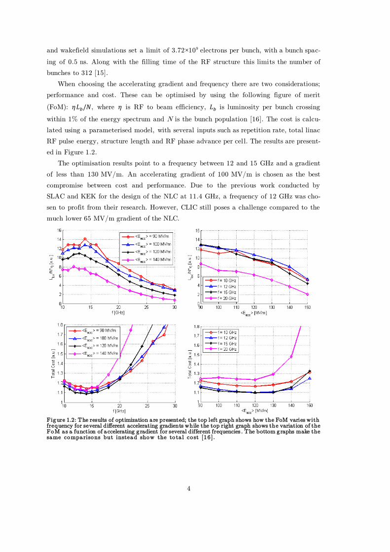
When choosing the accelerating gradient and frequency there are two considerations;
performance and cost. These can be optimised by using the following figure of merit
(FoM): 𝜂𝐿𝑏/𝑁, where 𝜂 is RF to beam efficiency, 𝐿𝑏 is luminosity per bunch crossing
within 1% of the energy spectrum and N is the bunch population [16]. The cost is calcu-
lated using a parameterised model, with several inputs such as repetition rate, total linac
RF pulse energy, structure length and RF phase advance per cel l. The results are present-
ed in Figure 1.2.
The optimisation results point to a frequency between 12 and 15 GHz and a gradient
of less than 130 MV/m. An accelerating gradient of 100 MV/m is chosen as the best
compromise between cost and performance. Due to the previous work conducted by
SLAC and KEK for the design of the NLC at 11.4 GHz, a frequency of 12 GHz was cho-
sen to profit from their research. However, CLIC still poses a challenge compared to the
much lower 65 MV/m gradient of the NLC.
Figure 1.2: The results of optimization a re presented; the top left graph shows how the FoM varies with frequency for several different accelerating gradients while the top right graph shows the variation of the FoM as a function of a ccelerating g radient for several different frequencies . The bottom g raphs make the same comparisons but instead show the to ta l co st [16 ].
5
1.4 RF Breakdown
The main limitation when trying to push the electric field in an accelerating cavity is
the breakdown rate (BDR). Even though these structures are operated under vacuum,
electromagnetic fields are high enough to cause arcs. So-called field emission sites are
thought to be responsible for triggering breakdown events. They are made from small (17 -
25 nm) geometric deformities on the copper surface, which are able to enhance the local
electric field 50-100 times, producing gradients as high as 10 GV/m [21] acting over a dis-
tance comparable to the geometric deformity.
The aforementioned limits for electric field, power flow and pulse temperature heating
all try to reduce the likelihood of breakdown. More recently the peak value on the surface
of the modified Poynting vector Sc has been used as the primary design constraint for the
BDR [22]. Sc aims to combine the physical effects of both field emission heating of the
geometrical defect with that of RF power flow. It has been shown to fit experimental data
of both travelling and standing wave, high gradient cavities over a broad frequency range.
The high power test facilities which are the main subject of this thesis aim to condi-
tion and process high gradient structures in a reliable and repeatable fashion so they a t-
tain the lowest possible breakdown rates. Once achieved, the facilities needed the capabi l-
ity to accurately determine breakdown rates as a function of gradient and pulse width.
1.5 Fabrication of High Gradient Structures
The baseline design for the CLIC accelerating structure is that of a stack of machined
disks bonded together to produce a complete multi-celled structure. The discs are individ-
ually machined using ultra precise, CNC, diamond milling machines. These machines
have been developed in industry and machined discs have achieved dimensional accuracies
of better than 2 𝜇𝑚 [23]. Quality controls including visual inspection for scratches and
dust, and metrology are carried out to ensure the discs meet the specification. If passed,
the discs are lightly etched to remove any surface impurities. The discs are stacked and
clamped together for an initial RF test, using a vector network analyser (VNA) to meas-
ure the transmission and reflection of the structure as a function of frequency. If the re-
sults match the theoretical performance to within the tuning range of the structure, the
discs are then diffusion bonded in a hydrogen atmosphere of 1 bar at 1020ºC for 1 hour
[24]. The couplers and cooling channels are then brazed on using an oven at a lower tem-
perature. The final fabrication stage is a 10 day bake out at 650ºC causing the hydrogen
absorbed in the bonding stage to diffuse out (along with other impurities). The structure
is then ready for the final tuning procedure.
In addition to test facility development, this thesis looks in detail at the testing of the
CLIC crab cavity whose function is described in section 1.8. The thesis includes infor-
mation on its design performance as validated as part of this work, its fabrication, its tun-
6
ing, its integration into the test stand, its conditioning and its final breakdown perfor-
mance.
1.6 RF Conditioning of High Gradient Structures
After the RF properties have been corrected and verified through the tuning process,
a structure is ready for high power RF. Initially, the full design gradient and pulse
lengths are not reachable. Although the fabrication steps are designed to clean and treat
the copper surface, they are not fully adequate to remove all field emission sites and im-
purities. Typically structures will be able to obtain accelerating gradients up to 10-
20 MV/m for pulse lengths of 50-100 ns before outgassing events start to occur. From this
point the power must be increased while trying to keep the vacuum level below an ac-
ceptable threshold (typically 10-7 mbar). Above 20MV/m electrical breakdowns in the
structure start to become the limiting effect when trying to increase the power. The pow-
er is now increased while trying to keep the breakdown rate (BDR) at the order of 10 -5
breakdowns per pulse (or about 2 per hour at 50-60 Hz). Once the nominal gradient has
been exceeded by a few percent, the pulse length is increased and the power level de-
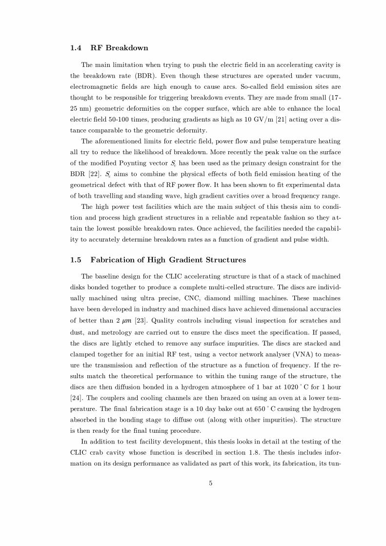
creased. This process is repeated until the nominal parameters are achieved (Figure 1.3).
Figure 1.3: Shows the processing history of a TD24R05 CLIC prototype structure tested a t KEK [25]. The red and g reen po ints show the a ccelerting g radient t he pulse width respectively .
At the end of the conditioning stage the structure runs at the design gradient and
pulse width of 100 MV/m and 250 ns respectively. The breakdown rate is also reduced by
1-2 orders of magnitude compared to the processing stage. The whole process takes more
than 1600 hours of RF on time at 60 Hz, i.e. 346 million pulses.
This thesis reports on the successful implementation of computer controlled condition-
ing procedures at the new CERN test facilities that are an advancement on what was
previously available at KEK and SLAC.
7
1.7 Standalone X-band Test Stands
CLIC uses a novel two beam accelerating scheme. This technology choice is justified
for very long machines because of the inherently high efficiency and scalability [26]. Klys-
trons were ruled out because high power X-band klystrons are relatively inefficient (40-
50%) and expensive. For CLIC, 35,000 units with factor 5 pulse compression would be
needed. However, for smaller machines and testing purposes, klystrons are the only feasi-
ble option.
SLAC have led the X-band klystron development since the late 80s when the NLC
project called for a klystron based, energy frontier machine. During a long R&D program
many klystrons were developed, each pushing the limit in RF peak power and pulse
length, the culmination of which is the XL-4 klystron [27]. The XL-4 operates at a fre-
quency of 11.424 GHz, with peak power and pulse length of 50 MW and 1.5 𝜇𝑠, respec-
tively. Able to pulse reliably at 120 Hz it continues to be the workhorse of X-band testing
at SLAC and KEK. The XL-5 which is an 11.994 GHz version of the XL-4, was developed
for use at European labs such as CERN, Elettra Sincrotrone Trieste and PSI. The recent
commercialisation of this tube by CPI (the VKX-8311A) is an important step in making
the test stands cheaper and more numerous. Since 2012 CERN has been operating an XL-
5 based high power test stand in order to test CLIC structures. Chapter 2 will discuss in
detail the design and performance of this test stand known as Xbox-1. The chapter will
identify shortcomings and outline work undertaken by the author to improve perfo r-
mance. A second CERN test stand known has Xbox-2 has been planned from 2012. Chap-
ter 3 describes the design and development of this test station. The author has taken
primary responsibility for most of the controls and hence these are described in the great-
est detail. Commissioning of Xbox-2 commenced in August 2014. The first structure to be
conditioned at Xbox-2 was the prototype CLIC crab cavity.
The recent development of the test stands is of great importance to the CLIC R&D
effort and also for other applications such as FELs. Multiple high-power test slots are
needed to test different versions of structures, different preparation techniques and to in-
crease the number of tested structures to determine production yield [28]. This effect is
compounded due to the fact that structures need a few thousand hours of RF on time in
order to be processed.
A third test stand to be known as Xbox-3 has been planned from 2013. The design of
the test stand is described in Chapter 4. The author has designed and commissioned the
RF front end.
8
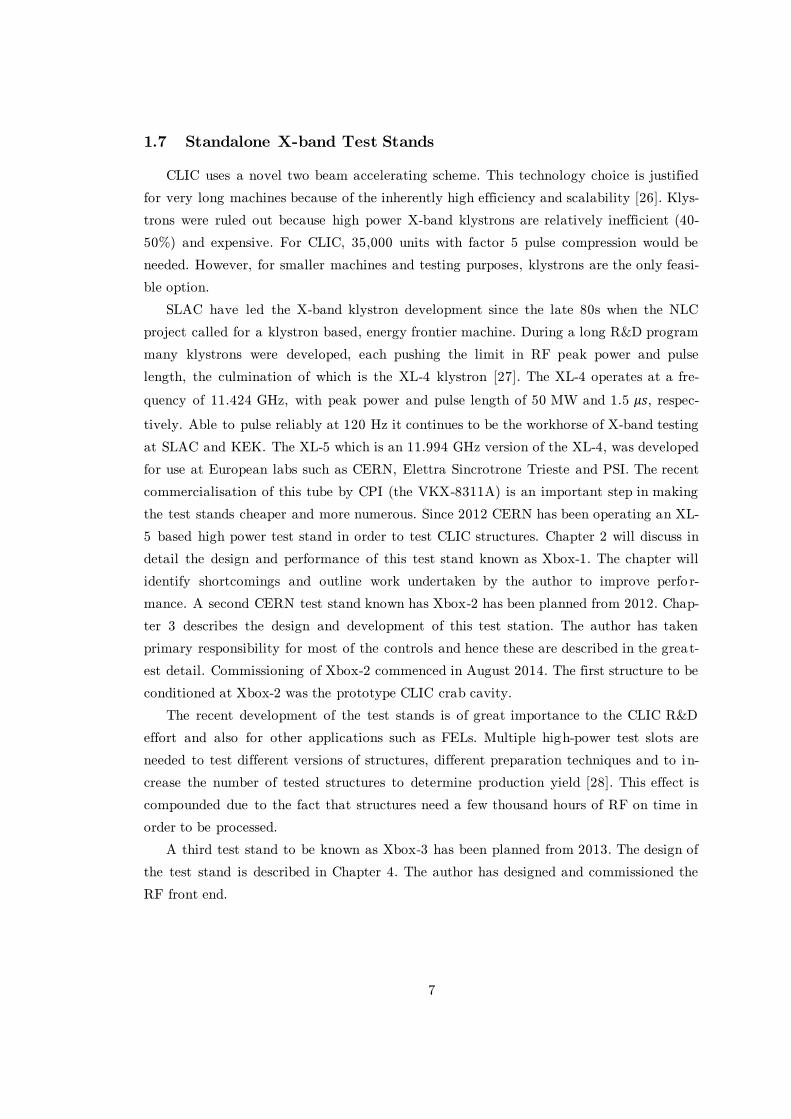
1.7.1 Test Stand layout
The current baseline design for the CLIC accelerating structure requires 63 MW of
RF power when properly beam loaded, therefore pulse compression is needed to increase
the peak RF power out of the klystron. With this consideration, Figure 1.4 shows the
general layout of a standalone test stand for CLIC.
Figure 1 .4 : Standa lone test stand layout with optiona l second structure.
The low level radio frequency (LLRF) generator produces a phase modulated, 12GHz,
1.5 𝜇𝑠 pulse which is amplified by a travelling wave tube (TWT) amplifier. This kilowatt
level signal is then amplified by the klystron up to 50 MW. The RF power is transmitted
through copper waveguide under ultra-high vacuum (UHV) conditions. The pulse com-
pressors that are typically used can increase the peak power by a factor of 3 when a
250 ns output pulse is produced [29]. The pulse can be fed into one or two devices under
test (DUTs) with the output power dissipated into high power loads. 50-60 dB directional
couplers are used for sampling RF signals with a dedicated LLRF system. The system can
also be used to test high power RF components such as; waveguide vacuum ports, RF
gate valves and mode converters.
Xbox-1 utilises this basic scheme. XBOX2 has an enhanced pulse compressor and
LLRF system. Xbox-3 is a new concept allowing many cavities to be conditioned and
tested simultaneously using lower power commercial klystrons.
1.8 Crossing angle and Crab Cavities
Crab cavities are likely to be required for TeV scale linear colliders and high luminos-
ity circular colliders. Detectors for all colliders require the interaction to take place within
a tightly defined region. At high energies this means that there must be a crossing angle
to reduce beam-beam effects and to define the interaction point [30]. Unlike the LHC or
other circular colliders, there is no second chance for a bunch collision. To increase the
luminosity, the electron bunches are tightly focussed. The proposed bunch size a t the IP
at CLIC is given in Table 1.1 [31].

9
Horizontal bunch size 45 nm
Vertical bunch size 1 nm
Bunch length 44 𝜇m
Table 1 .1 : Bunch dimensions a t the CLIC interaction po int.
The bunch shape is that of a long piece of ribbon. This is important when consider-
ing the interaction of colliding bunches at the IP as illustrated in Figure 1.5.
Figure 1 .5 : Intera ction o f two beams with and without crabbing .
The bottom part of the figure shows how a crossing angle reduces the area of interac-
tion between the colliding bunches. At CLIC the luminosity would be reduced by 90%
due to this effect without corrective action. The top section of Figure 1.5 shows how the
bunches are rotated by momentum kicks to the front and back of the bunch, thus increa s-
ing the area of interaction. A deflecting cavity operated 90ºout of phase can achieve the
desired effect and is known as a crab cavity [32]. Here, the centre of the bunch is aligned
with the zero-crossing of the magnetic field and the front and rear of the bunch receive
equal and opposite momentum kicks [33]. A major objective of this work has been the
high power testing of the first CLIC crab cavity prototype.
1.9 Other Applications of high gradient X-band technology
Accelerator applications that require compact designs will profit from moving to high-
er frequencies. Transverse size is reduced proportional to the wavelength, thus reducing
size and weight. The main limitation is that the iris radii are small, amplifying wakefields
and causing problems for beams with large transverse dimensions. However, for many ap-
plications these limitations can be overcome. Light sources, medical and security linacs
can and do profit from X-band technologies. For example, at the Cockcroft Institute, UK,
a 1 MeV compact linac has been designed and tested for the purpose of making a portable
X-ray security scanner [34]. X-band electron linacs have been designed for radiotherapy,
10
as their reduced weight allows them to be mounted on modest gantries and robotic arms
[35].
X-band technology has been successfully utilized by various types of light source.
Compact Compton sources have been developed using CLIC like technology, such as
Compton source at LLNL [36]. X-ray free-electron lasers (FELs) use bunch compression
to produce a very short electron bunch. This bunch is passed through an undulator to
produce a coherent X-ray pulse. Typically an S-band photo-cathode gun and accelerator
is used to produce an electron beam of 70-100MeV. As with any RF accelerator there will
be an energy spread in the bunch due to the non-zero size of the electron bunch compared
with the RF wavelength. Furthermore, this energy spread is non-linear due to the curva-
ture of the sinusoidal field. The non-linear component decreases the effectiveness of the
bunch compressor. The compression efficiency can be improved by linearizing the energy
spread of the bunch. An RF frequency that is a higher harmonic of the main accelerating
frequency is needed for linearization. X-band accelerating cavities are used for this pur-
pose at LCLS, SWISSFEL and FERMI [37], [38], [39].
1.10 High phase stability
For many accelerator applications phase stability and highly precise synchronisation can
be very important. For example at large scale FEL facilities X-ray pulses that are only a
few tens of femtoseconds wide are produced. Many users of these facilities require that the
sample is first excited by a laser ‘pump’ and probed by the X-ray pulse sometime after.
These so-called ‘pump and probe’ experiments need to be synchronised over many hun-
dreds of meters [40].
The phasing of the crab cavities at CLIC is extremely important. If the phase between
the zero crossing of the B-field in the deflecting cavity and bunch centre is non-zero, the
bunch will be rotated about a point which is not its centre, adding a deflection to the
bunch. If for each crab cavity the offsets are different, the colliding bunches will miss or
partially miss. In order to keep the luminosity reduction below 2% the two crab cavities
must be phased to within 20 milli-degrees at 12 GHz [32]. This translated to a timing er-
ror of just 4.4 fs between the two cavities. Part of this work has been to improve our abil-
ity to accurately measure and record phase fluctuations during short high power pulse.
1.11 Summary
After the discovery of the Higgs-like particle at the LHC, some in the physics community
desire a lepton collider. CLIC is an electron-positron collider that can perform precision
measurements on the Higgs and also push past the energy reach of the LHC. Physics be-
yond the standard model can also be explored. CLIC has been optimised to produce the
highest energy leptons with a competitive luminosity to that of the LHC. X-band tech-
nology was shown to give the best performance to cost ratio in the optimisation study.
11
Mechanisms of breakdown were introduced and ideas to reduce the breakdown rate have
been explored. Due to the challenging 100 MV/m gradient chosen and new 12 GHz fre-
quency, standalone test stands have been developed to test new RF components and to
measure the performance of prototype CLIC accelerating structures. Due to the elongated
bunch shape and crossing angle at CLIC’s interaction point, luminosity loss due to the
crossing angle is very high. The addition of a pair of crab cavities can mitigate the prob-
lem but a high degree of phase synchronisation is needed. Other applications have profit-
ed from CLIC technology such as FELs, security linacs and medical linacs. The im-
portance of phase synchronisation has been established for the CLIC crab cavities and
FEL applications.
In this thesis, chapter 2 focusses on the first test stand built at CERN and work un-
dertaken by the author to upgrade the control and LLRF systems. Chapter 3 goes into
detail of the design of the second high power test stand at CERN. New waveguide com-
ponents have been developed including a new pulse compressor which was tuned and test-
ed. The new LLRF and control systems for Xbox-2 were developed and tested by the au-
thor. Finally the test stand was installed and fully commissioned up to high power.
Chapter 4 gives a design layout for the third high power test stand, which combines 4
klystrons to vastly increase testing capacity at CERN. Proof of principle experiments
have been conducted in the laboratory and the first of the 4 power units have been com-
missioned by the author.
Chapter 5 outlines the complete development of an un-damped CLIC crab cavity pro-
totype. HFSS [41] simulations are carried out by the author to verify the surface field
quantities and deflecting voltage and to facilitate tuning. The chapter then describes how
the cavity was manufactured, tuned and tested to 50 MW.
12
Chapter 2
2 Xbox-1: CERN’s first 12 GHz standalone test stand
Xbox-1 is the first standalone test stand to be operated at CERN. This chapter will
discuss the need for such an experiment, the design considerations and the operational
experience. Design issues are explored in detail, with solutions presented and validated.
2.1 Reasons for standalone test stands
As discussed in the introduction, the primary objective of the test stands is to support
the development of high-gradient, accelerating structures and high-power, 50-100 MW
range, RF components for the CLIC project [15]. Before Xbox-1 started operations the
only place where 12 GHz power was available at the pulse lengths and power required to
test CLIC accelerating structures was at the CLIC Test Facility 3 (CTF-3) at CERN.
The CTF-3 experiment uses an S-band linac and a series of combination steps to produce
a high current (30 A) beam with a 12 GHz bunch train structure. The bunch train is then
decelerated using specially designed RF structures called ‘Power Extraction and Transfer
Structures’ or PETS. The kinetic energy of the beam is transferred into electromagnetic
energy which can be used to power high gradient structures [42].
CTF-3 has proved to be very successful in validating the CLIC two beam concept, by
succeeding in transferring power from the drive beam to a test beam using the PETS and
CLIC prototype accelerating structures. However, for high gradient testing purposes the
cost and maintenance required to operate a complete accelerator facility is not justified.
The drive beam generation complex at CTF-3 uses a 70 m linac driven by 14, 40 MW S-
band klystrons, a 42 m long delay loop and a 84 m long combiner ring to produce the
120 MeV drive beam. The installed testing capacity is for two prototype RF structures at
a maximum pulse repetition rate of 5 Hz [43]. A 50 MW, klystron based test stand is ca-
pable of at least 50 Hz operation with the possibility of pulsing at 100 Hz. Each klystron
is capable of testing two accelerating structures meaning a single klystron could have up
to 20 times the testing capacity that is available at CTF-3. The availability of multiple
testing slots is crucial in understanding different structure designs, different preparation
techniques and to gain good statistics in order to determine production yield.
The commissioning and operation of the test stands also drives the development of
high power components and LLRF systems. Recent studies have explored the possibility
of a klystron-based initial energy version of CLIC [44], for which the test stands are an
important research tool. Other areas in which X-band technology can be applied are med-
ical linacs, XFEL linacs, high-frequency and high-gradient beam manipulation devices
13
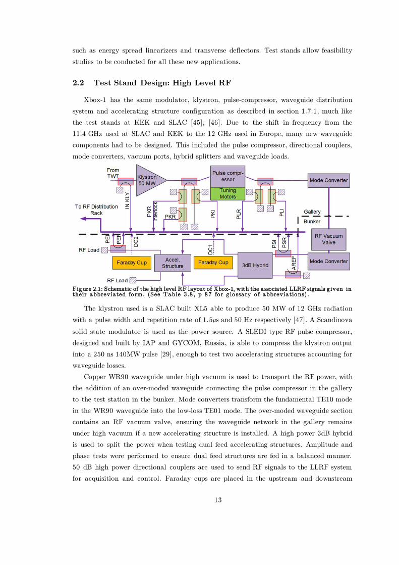
such as energy spread linearizers and transverse deflectors. Test stands allow feasibility
studies to be conducted for all these new applications.
2.2 Test Stand Design: High Level RF
Xbox-1 has the same modulator, klystron, pulse-compressor, waveguide distribution
system and accelerating structure configuration as described in section 1.7.1, much like
the test stands at KEK and SLAC [45], [46]. Due to the shift in frequency from the
11.4 GHz used at SLAC and KEK to the 12 GHz used in Europe, many new waveguide
components had to be designed. This included the pulse compressor, directional couplers,
mode converters, vacuum ports, hybrid splitters and waveguide loads.
Figure 2.1: Schematic of the high level RF layout of Xbox-1, with the a ssociated LLRF signals g iven in their abbrevia ted fo rm. (See Table 3 .8 , p 87 fo r g lo ssa ry o f abbrevia tions) .
The klystron used is a SLAC built XL5 able to produce 50 MW of 12 GHz radiation
with a pulse width and repetition rate of 1.5𝜇s and 50 Hz respectively [47]. A Scandinova
solid state modulator is used as the power source. A SLEDI type RF pulse compressor,
designed and built by IAP and GYCOM, Russia, is able to compress the klystron output
into a 250 ns 140MW pulse [29], enough to test two accelerating structures accounting for
waveguide losses.
Copper WR90 waveguide under high vacuum is used to transport the RF power, with
the addition of an over-moded waveguide connecting the pulse compressor in the gallery
to the test station in the bunker. Mode converters transform the fundamental TE10 mode
in the WR90 waveguide into the low-loss TE01 mode. The over-moded waveguide section
contains an RF vacuum valve, ensuring the waveguide network in the gallery remains
under high vacuum if a new accelerating structure is installed. A high power 3dB hybrid
is used to split the power when testing dual feed accelerating structures. Amplitude and
phase tests were performed to ensure dual feed structures are fed in a balanced manner.
50 dB high power directional couplers are used to send RF signals to the LLRF system
for acquisition and control. Faraday cups are placed in the upstream and downstream
14
directions along the structure’s beam axis to measure dark current and detect breakdown
events in the structure [28].
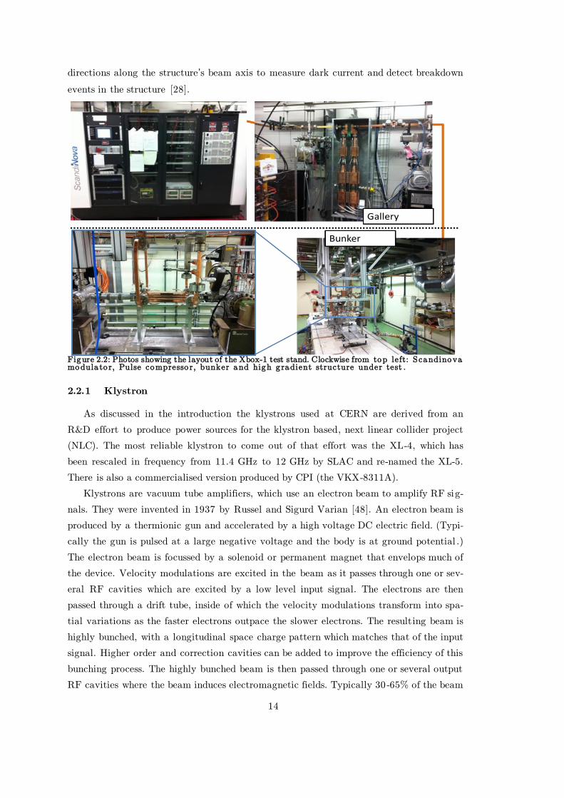
Figure 2.2: Photos showing the layout of the Xbox-1 test stand. Clockwise from top left: Scandinova modula to r, Pulse compresso r, bunker and high g radient structure under test .
2.2.1 Klystron
As discussed in the introduction the klystrons used at CERN are derived from an
R&D effort to produce power sources for the klystron based, next linear collider project
(NLC). The most reliable klystron to come out of that effort was the XL-4, which has
been rescaled in frequency from 11.4 GHz to 12 GHz by SLAC and re-named the XL-5.
There is also a commercialised version produced by CPI (the VKX-8311A).
Klystrons are vacuum tube amplifiers, which use an electron beam to amplify RF sig-
nals. They were invented in 1937 by Russel and Sigurd Varian [48]. An electron beam is
produced by a thermionic gun and accelerated by a high voltage DC electric field. (Typi-
cally the gun is pulsed at a large negative voltage and the body is at ground potential .)
The electron beam is focussed by a solenoid or permanent magnet that envelops much of
the device. Velocity modulations are excited in the beam as it passes through one or sev-
eral RF cavities which are excited by a low level input signal. The electrons are then
passed through a drift tube, inside of which the velocity modulations transform into spa-
tial variations as the faster electrons outpace the slower electrons. The resulting beam is
highly bunched, with a longitudinal space charge pattern which matches that of the input
signal. Higher order and correction cavities can be added to improve the efficiency of this
bunching process. The highly bunched beam is then passed through one or several output
RF cavities where the beam induces electromagnetic fields. Typically 30-65% of the beam

15
power is transmitted into the RF. In this way multiple MW of peak power can be ex-
tracted from the beam. The power is coupled out of the cavities via waveguides and
passed through an RF window towards the desired load.
2.2.2 Modulator
The SLAC XL-5 and the CPI VKX-8311A variant produce 50 MW of peak RF power
and have a perveance of 1.18 𝜇𝑃. The unit micro-perveance, 𝜇𝑃 is defined as 𝜇𝑃 =
106𝐼𝑉−1.5, where I and V are the klystron current and voltage. However, their efficiency is
of the order of 40 %, meaning their power source has to be able to provide a peak pulsed
power of 125 MW. This power level and perveance demands a voltage of 410 kV and a
current of 310 A. Klystron modulators are able to provide such pulses. However, the high
voltages needed are particularly challenging, consequently there are few vendors capable
of producing such a device. Furthermore, the test stand at CERN is required to have high
flexibility and for this reason a solid state modulator was chosen to power the XL-5. The
only company capable of manufacturing such a device was Scandinova.
The Scandinova K-3 modulator is a collection of different components that work to-
gether to produce a high voltage pulse. There are four main components; charging power
supplies, solid state switches, a pulse transformer and tuning circuit. The charging power
supplies covert the 3-phase, 415 V mains voltage into a DC voltage of up to 1400 V,
which is stored in a capacitor bank. The charge stored in the capacitor bank is then
switched through a bank of solid state switches. The switched pulse is transferred through
a tuning circuit into a pulse transformer with a transformer ratio of 1:360, thus able to
step up the 1400 V to 500 kV. Using this transformer ratio and the 310 A that the klys-
tron requires, it is easy to calculate that nearly 112 kA of current needs to be switched on
the timescales of micro-seconds. It is here that the greatest technological challenge is pre-
sented. In order to reduce the current load on the switches, the current is split evenly be-
tween 60 solid state switches, each conducting 1.9 kA of current. This is where the flexi-
bility of a solid state modulator is made apparent. The pulse length is controlled directly
by the length of time that the switches remain closed.
Due to the high voltages involved, the pulse transformer and klystron gun are sub-
merged in a bath of insulating oil. The oil quality is checked periodically for signs of
breakdown, which causes the oil to degrade.
The modulator contains a control system which is able to monitor the klystron’s vacuum,
temperature and power dissipation and interlock the system if there are any issues.
2.2.3 Pulse Compressor Operation with a 180º Phase Flip
The SLED-I pulse compressor was invented at SLAC in 1973, with the aim
of doubling the SLAC linac’s energy [49]. The main principle of operation is that RF en-
ergy from a klystron is stored in two high Q cavities during a pulse. Towards the end of

16
the pulse the cavities are emptied by reversing the phase of the input pulse from the klys-
tron. The cavities are emptied in a shorter timeframe compared to that in which the cavi-
ties were filled. Conservation of energy requires that the peak power is increased as the
pulse is compressed in time. Referenced to the same impedance, a cavity filled from a
waveguide will have twice the filling voltage which will be in opposition (shifted by 180
degrees) compared to the waveguide voltage. Once the cavity is full and if the filling volt-
age is reversed, an outgoing wave with three times the filling voltage is generated in the
waveguide. This means that a maximum theoretical pulse compression of 9 is possible at
the instant the filling voltage is reversed. The need to generate a pulse of finite width and
allowing for losses then typically the peak power can only be increased by a factor of 5-7.
Figure 2 .3 : Shows a simple schematic o f a SLED I pulse compresso r.
Two cavities are used, coupled to a 3 dB hybrid in order to direct the power flow
away from the klystron, as shown in Figure 2.3. A single cavity with a circulator could
also be used to form a pulse compressor, but unfortunately 200MW X band circulators do
not exist and indeed would be extraordinarily difficult to develop.
Following Farkas et al. [49] a simplistic analysis obtains fields by considering the con-
servation of power in the system for a single cavity. It ignores the hybrid coupler but as-
sumes that ingoing power can be separated from outgoing power. There are four quanti-
ties to consider; the input power 𝑃𝑖 , the outward going power from the iris 𝑃𝑟 , the power
lost in the cavity 𝑃𝑐 , and the stored power in the cavity 𝑑𝑊𝑐
𝑑𝑡, where 𝑊𝑐 is the energy stored
at time 𝑡. The quantities follow the relation:
𝑃𝑖 = 𝑃𝑟 + 𝑃𝑐 +𝑑𝑊𝑐
𝑑𝑡 (2.1)
The stored energy can be expressed in terms of the unloaded Q-factor Q0, the dissipated
power 𝑃𝑐 and the angular frequency 𝜔 to give:
𝑊𝑐 =𝑄0𝑃𝑐𝜔
(2.2)
Let 𝑉𝑐 be the cavity field and defining the cavity shunt impedance 𝑅 then:
𝑃𝑐 =𝑉𝑐
2
𝑅 (2.3)

17
Let 𝑉𝑖 be the voltage of the forward wave in transmission line with impedance 𝑍 then:
𝑃𝑖 =𝑉𝑖
2
𝑍 (2.4)
Let 𝑉𝑟 be the voltage of the backward wave in transmission line with impedance 𝑍
then:
𝑃𝑟 =𝑉𝑟
2
𝑍 (2.5)
The voltage of the forward wave 𝑉𝑖 plus the voltage of the backward wave 𝑉𝑟 equals
the cavity voltage 𝑉𝑐 hence:
𝑉𝑟 = 𝑉𝑐 − 𝑉𝑖 (2.6)
Now by substituting equations (2.2)-(2.6) into (2.1), in order to retain just 𝑉𝑐 and 𝑉𝑖
gives:
𝑉𝑖2
𝑍=
(𝑉𝑐 − 𝑉𝑖)2
𝑍+
𝑉𝑐2
𝑅+
2𝑄𝑜
𝑅𝜔
𝑉𝑐𝑑𝑉𝑐𝑑𝑡
(2.7)
This simplifies to:
2𝑉𝑖 = (1 +𝑍
𝑅)𝑉𝑐 +
2𝑍
𝑅
𝑄𝑜
𝜔
𝑑𝑉𝑐𝑑𝑡
(2.8)
It is also useful to define the cavity coupling coefficient, as the ratio of power emitted
from the coupling aperture to that dissipated in the cavity walls so that:
𝛽 =𝑃𝑟𝑃𝑐
=𝑄𝑜
𝑄𝑒
=𝑅
𝑍 (2.9)
Hence equation (2.8) can be re-written as:
2𝛽
1 + 𝛽𝑉𝑖 = 𝑉𝑐 +
2𝑄𝑜
(1 + 𝛽)𝜔
𝑑𝑉𝑐𝑑𝑡
(2.10)
We can define the loaded Q-factor 𝑄𝐿 as:
1
𝑄𝐿
=1
𝑄𝑜
+1
𝑄𝑒
(2.11)
Then from equation (2.9):
𝑄𝐿 =𝑄𝑜
1+ 𝛽 (2.12)
We can define:
𝛼 =2𝛽
1+ 𝛽 (2.13)
We can also define:
𝑇𝑐 =2𝑄𝑜
(1 + 𝛽)𝜔=
2𝑄𝐿
𝜔 (2.14)
Using equations (2.13) and (2.14), equation (2.10) can be rewritten:
𝑇𝑐
𝑑𝑉𝑐𝑑𝑡
+ 𝑉𝑐 = 𝛼𝑉𝑖 (2.15)
As described earlier, in order to get useful compression for the device, the input field
is held constant and then flipped by 180 degrees at time tf. The end of the pulse is at
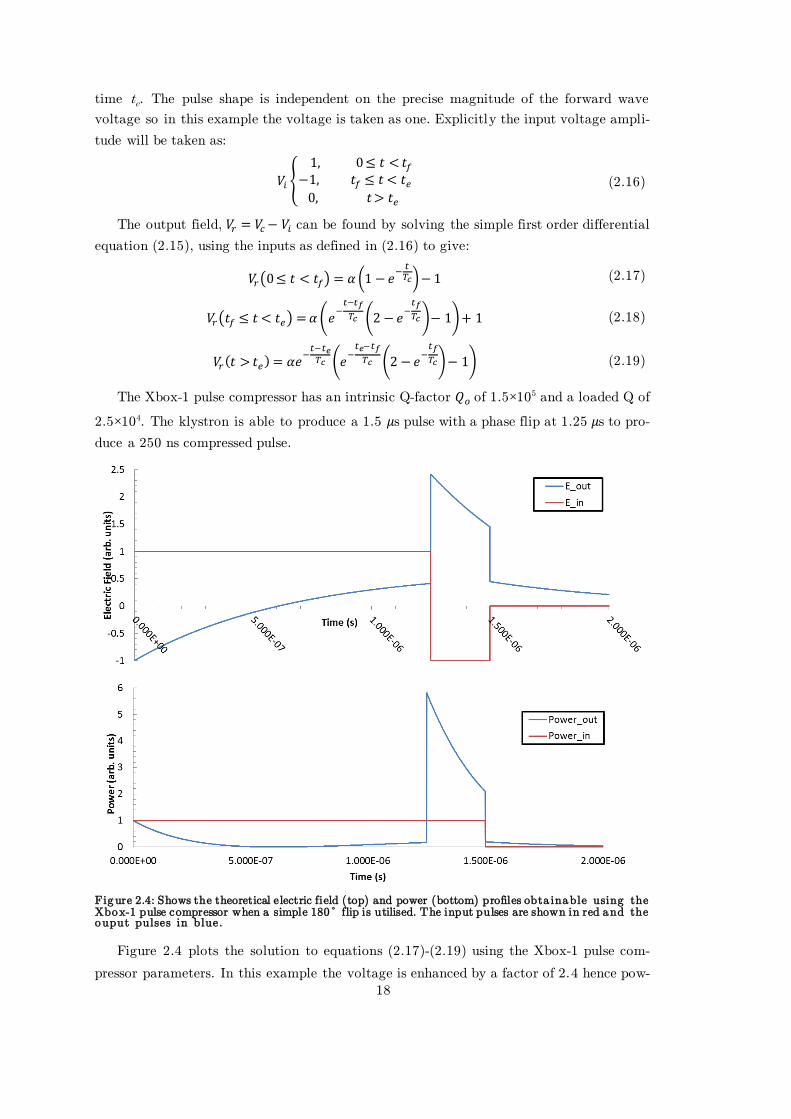
18
time te. The pulse shape is independent on the precise magnitude of the forward wave
voltage so in this example the voltage is taken as one. Explicitly the input voltage ampli-
tude will be taken as:
𝑉𝑖 {
1, 0≤ 𝑡 < 𝑡𝑓−1, 𝑡𝑓 ≤ 𝑡 < 𝑡𝑒0, 𝑡> 𝑡𝑒
(2.16)
The output field, 𝑉𝑟 = 𝑉𝑐 − 𝑉𝑖 can be found by solving the simple first order differential
equation (2.15), using the inputs as defined in (2.16) to give:
𝑉𝑟(0≤ 𝑡 < 𝑡𝑓) = 𝛼 (1 − 𝑒−
𝑡𝑇𝑐)− 1 (2.17)
𝑉𝑟(𝑡𝑓 ≤ 𝑡 < 𝑡𝑒) = 𝛼(𝑒−
𝑡−𝑡𝑓𝑇𝑐 (2 − 𝑒
−𝑡𝑓𝑇𝑐)− 1)+ 1 (2.18)
𝑉𝑟(𝑡 > 𝑡𝑒) = 𝛼𝑒−
𝑡−𝑡𝑒𝑇𝑐 (𝑒
−𝑡𝑒−𝑡𝑓
𝑇𝑐 (2 − 𝑒−
𝑡𝑓𝑇𝑐)− 1) (2.19)
The Xbox-1 pulse compressor has an intrinsic Q-factor 𝑄𝑜 of 1.5×10⁵ and a loaded Q of
2.5×10⁴. The klystron is able to produce a 1.5 𝜇s pulse with a phase flip at 1.25 𝜇s to pro-
duce a 250 ns compressed pulse.
Figure 2.4: Shows the theoretical electric field (top) and power (bottom) profiles obta inable using the Xbox-1 pulse compressor when a simple 180º flip is utilised. The input pulses are shown in red and the ouput pulses in blue.
Figure 2.4 plots the solution to equations (2.17)-(2.19) using the Xbox-1 pulse com-
pressor parameters. In this example the voltage is enhanced by a factor of 2.4 hence pow-
19
er is enhanced by a factor of 5.8. The real world performance will be lower due to losses
in the RF 3 dB hybrid coupler and waveguide network. This pulse is useful for single
bunch machines such as FELs and some medical linacs, but for longer pulse machines, its
non-uniformity will cause a large energy spread in the bunch train. Moreover, for the
purpose of testing CLIC structures, this pulse shape is very dissimilar to the pulse that
CLIC will use (a square pulse with a short ramp).
2.2.4 Pulse Compressor Operation with a Phase Ramp
The pulse shape can be flattened by modulating the phase during the high power
pulse [50]. For the analysis of the previous section as determined by equation (2.17), just
before the field is reversed and when the fill time 𝑡𝑓 is much greater than 𝑇𝑐 then
𝑉𝑟(𝑡𝑓−) = (𝛼 − 1)𝑉𝑖𝑛 where 𝑉𝑖𝑛 is the ingoing voltage. For the over-coupled cavity with
𝛽 ≫ 1, then 𝛼~2 so 𝑉𝑟(𝑡𝑓−)~𝑉𝑖𝑛 . After the phase flip as determined by equation (2.18),
with 𝑡𝑓 = 𝑡 then 𝑉𝑟(𝑡𝑓+)= (𝛼 + 1)𝑉𝑖𝑛 which shows that the output voltage increases by 2𝑉𝑖𝑛.
If however the field is not fully reversed but moved by 90 degrees, it can be shown a
factor of only √2𝑉𝑖𝑛 is added. Over the rest of the pulse the phase is ramped to 180 de-
grees, adding more field to compensate for the decay of the pulse. With careful phase pro-
gramming the pulse can be made to be flat. The output phase variation will be half that
of the input phase variation, which is still significant and will cause non-uniform beam
loading if a beam is present. However, for high gradient testing purposes the presence of
the phase ramp will not be a problem. Typically the compression ratio will be reduced by
a factor of approximately 2 compared to the case presented in Figure 2.4.
The principle that a perfectly flat top amplitude pulse can be achieved and the neces-
sary phase ramp needed for a perfectly tuned pulse compressor has been derived by Fiebig
and Schieblich [50].
The cavity is modelled as a parallel LCR circuit connected to a generator. Using the
standard accelerator notation the differential equation for the driven cavity can be writ-
ten:
�̈� +𝜔0
𝑄𝐿
�̇� + 𝜔02𝑉 =
2𝜔0
𝑄𝑒
𝑑
𝑑𝑡{𝐹 cos(𝜔𝑡 + 𝜑)} (2.20)
where cavity voltage 𝑉, forward wave amplitude 𝐹 and forward phase 𝜑 are real. This
differential equation can be solved exactly for periods of time when 𝐹 and 𝜑 do not vary.
When 𝐹 and 𝜑 do vary it is convenient to simplify the equation by taking out the high
frequency oscillation and just analysing the envelope of the wave and i ts phase. Manipu-
lation of equation (2.20) is easier using a complex notation so we write it in the form:
�̈� +𝜔0
𝑄𝐿
�̇� + 𝜔02𝑉=
2𝜔0
𝑄𝑒
𝑅𝑒{(�̇� + 𝑗𝜔𝐹)𝑒𝑗(𝜔𝑡+𝜑)} (2.21)

20
In order to focus on the envelope we assume the high free oscillation is known by
looking for a solution of the form:
𝑉 = 𝑅𝑒{𝑉𝑐𝑒𝑗𝜔0𝑡} (2.22)
Where 𝑉𝑐 is a complex phasor being sought. Differentiating equation (2.22) with re-
spect to time gives:
�̇� = 𝑅𝑒{(�̇�𝑐 + 𝑗𝜔0𝑉𝑐)𝑒𝑗𝜔0𝑡} (2.23)
And for a second time gives:
�̈� = 𝑅𝑒{(�̈�𝑐 + 2𝑗𝜔0�̇�𝑐 − 𝜔02𝑉𝑐)𝑒
𝑗𝜔0𝑡} (2.24)
Substitution of equations (2.22)-(2.24) into equation (2.21) and not explicitly specify-
ing that real part must be taken gives:
�̈�𝑐 + 2𝑗𝜔0�̇�𝑐 − 𝜔02𝑉𝑐 +
𝜔0
𝑄𝐿
(�̇�𝑐 + 𝑗𝜔0𝑉𝑐)+ 𝜔02𝑉𝑐 =
2𝜔0
𝑄𝑒
(�̇�+ 𝑗𝜔𝐹)𝑒𝑗(𝜔−𝜔0)𝑡𝑒𝑗𝜑
which reduces to:
�̈�𝑐 + 𝜔0(2𝑗 +1
𝑄𝐿
)�̇�𝑐 + 𝑗𝜔0
2
𝑄𝐿
𝑉𝑐 =2𝜔0
𝑄𝑒
(�̇�+ 𝑗𝜔𝐹)𝑒𝑗(𝜔−𝜔0)𝑡𝑒𝑗𝜑 (2.25)
If 𝐹 is slowly varying then the phasor 𝑉𝑐 will be slowly varying hence we can ignore �̈�𝑐.
For all practical accelerator and pulse compressor cavities 𝑄𝐿 is on the order of 103-108,
hence it is always acceptable to make the approximation that (2𝑗 +1
𝑄𝐿)~2𝑗. With these
approximations equation (2.25) becomes:
�̇�𝑐 +𝜔0
2𝑄𝐿
𝑉𝑐 =1
𝑄𝑒
(−𝑗�̇�+ 𝜔𝐹)𝑒𝑗(𝜔−𝜔0)𝑡𝑒𝑗𝜑 (2.26)
For the pulse compressor the amplitude of the forward voltage 𝐹 is constant hence
�̇� = 0, so equation (2.26) becomes:
2𝑄𝐿
𝜔0
�̇�𝑐 + 𝑉𝑐 =2𝑄𝐿
𝑄𝑒
𝜔
𝜔0
𝐹𝑒𝑗(𝜔−𝜔0)𝑡𝑒𝑗𝜑 (2.27)
This is a generalisation of equation (2.15) which allows the phase of the drive to vary
and the compressor cavities to be out of tune. Fiebig and Schieblich assume that the cavi-
ties are perfectly tuned by setting 𝜔 = 𝜔0. Also by using equations (2.9), (2.12), (2.13) and
(2.14), equation (2.27) can be expressed as:
𝑇𝑐�̇�𝑐 + 𝑉𝑐 = 𝛼𝐹𝑒𝑗𝜑 (2.28)
If we let the input voltage:
𝑉𝑖 = 𝐹𝑒𝑗𝜑 (2.29)
Then (2.28), becomes:
𝑇𝑐�̇�𝑐 + 𝑉𝑐 = 𝛼𝑉𝑖 (2.30)
This is identical to that derived by the energy analysis except it is now seen to be va l-
id for complex time varying phasors. Let 𝑉𝑟 be the backward voltage phasor in the trans-
mission line at the cavity hence as before:

21
𝑉𝑐 = 𝑉𝑖 + 𝑉𝑟 (2.31)
Then we can insert equation (2.31) into equation (2.30) to eliminate 𝑉𝑐:
𝑇𝑐𝑉�̇� + 𝑉𝑟 = −𝑇𝑐𝑉�̇� + (𝛼− 1)𝑉𝑖 (2.32)
The reflection coefficient can be defined as:
Γ = 𝛼 − 1 =2𝛽
1 + 𝛽− 1 =
1 − 𝛽
1 + 𝛽 (2.33)
Hence, equation (2.32) becomes:
𝑇𝑐𝑉�̇� + 𝑉𝑟 = −𝑇𝑐𝑉�̇�+ Γ𝑉𝑖 (2.34)
For any instantaneous change in the forward voltage’s amplitude or phase ∆𝑉𝑐 = 0 be-
cause the cavity has capacitance and takes some time to react. Therefore from equation
(2.31) one must have (for instantaneous changes):
∆𝑉𝑖 = −∆𝑉𝑟 (2.35)
Let 𝑉𝑖 switch from zero to 𝑉0 at 𝑡 = 0 so that 𝑉𝑟 = −𝑉0 at 𝑡 = 0. For the period 𝑡 = 0 to
𝑡 = 𝑡𝑓 let 𝑉𝑖 = 𝑉0 = constant such that 𝑉�̇� = 0.
Using the above assumptions and integrating equation (2.34) gives:
∫𝑑𝑉𝑟
𝑉𝑟−Γ𝑉0=
−1
𝑇𝑐
𝑉𝑟
−𝑉0
∫ 𝑑𝑡𝑡
0
ln(𝑉𝑟(𝑡)− Γ𝑉0
−𝑉0−Γ𝑉0
) =−𝑡
𝑇𝑐
𝑉𝑟(𝑡) = 𝑉0{Γ− (1 − Γ)𝑒−𝑡 𝑇𝑐⁄ } 0< 𝑡 < 𝑡𝑓 (2.36)
Suppose the forward voltage switches from 𝑉0 to 𝑉0𝑒𝑗𝜃1 at 𝑡 = 𝑡𝑓 then:
∆𝑉𝑟 = −∆𝑉𝑖 = 𝑉0(1− 𝑒𝑗𝜃1) (2.37)
𝑉𝑟(0+) = 𝑉0{1− 𝑒𝑗𝜃1 + Γ− (1 + Γ)𝑒−𝑡𝑓 𝑇𝑐⁄ } (2.38)
If the phase has variation 𝜃(𝑡) after 𝑡 = 𝑡𝑓 so that:
𝑉𝑖(𝑡) = 𝑉0𝑒𝑗𝜃(𝑡) 𝑡> 𝑡𝑓 (2.39)
Then equation (2.34) becomes:
𝑇𝑐𝑉�̇� + 𝑉𝑟 = (−𝑗𝑇𝑐�̇� + Γ)𝑉0𝑒𝑗𝜃 (2.40)
Thus the reflected field is determined by:
∫𝑑𝑉𝑟
𝑉𝑟 + (𝑗𝑇𝑐�̇� − Γ)𝑉0𝑒𝑗𝜃
=−1
𝑇𝑐
𝑉𝑟
𝑉(0+)∫ 𝑑𝑡
𝑡
𝑡𝑓
𝑡 > 𝑡𝑓 (2.41)
Instead of solving this problem for 𝑉𝑟(𝑡), Fiebig and Schieblich determine the function
𝜃(𝑡) that gives constant 𝑉𝑟.
A SLED type RF pulse compressor uses a hybrid 3dB coupler to combine output from
the two cavities. The S matrix for a hybrid 3dB coupler is:

22
𝑆𝐻 =1
√2[
0 1 ±𝑗 01 0 0 ±𝑗±𝑗 0 0 10 ±𝑗 1 0
] (2.42)
Port 1 is the amplifier, ports 2 and 3 are the pulse compressor cavities and port 4 is
the load. Initially the amplifier output is 𝑉0 and there is no reflected power, so the inputs
to the pulse compressor cavities are determined as:
1
√2[
0 1 ±𝑗 01 0 0 ±𝑗±𝑗 0 0 10 ±𝑗 1 0
][
𝑉0
000
] =1
√2[
0𝑉0
𝑗𝑉0
0
] (2.43)
Once filling is complete and for 𝛿𝜔
𝜔0≪
1
2𝑄𝐿 the backward power for each cavity is de-
termined by equation (2.36); here for brevity we assume that 𝑡𝑓 is very large. We also as-
sume that the cavities have slightly different tunes causing their outputs to differ by 𝛿
from a mean value. The output to the cavity after filling but before the phase switch is
then given as:
1
√2[
0 1 𝑗 01 0 0 𝑗𝑗 0 0 10 𝑗 1 0
]
[
𝑉0
(𝑉0Γ+ δ) √2⁄
𝑗(𝑉0Γ− δ) √2⁄0 ]
≅
1
√2[
δ
𝑉0 √2⁄
𝑗 𝑉0 √2⁄𝑗𝑉0Γ ]
(2.44)
At this point, power to the load equals the input power minus losses encompassed by
the coefficient and with a 90 degree phase shift. Using equation (2.37) to determine the
output from a cavity after the input phase is switched, then at this instant the outputs
are given as:
1
√2[
0 1 𝑗 01 0 0 𝑗𝑗 0 0 10 𝑗 1 0
]
[
−𝑉0𝑒𝑗𝜃1
(𝑉0(1− 𝑒𝑗𝜃1 + Γ) + δ) √2⁄
𝑗(𝑉0(1− 𝑒𝑗𝜃1 + Γ)− δ) √2⁄
0 ]
≅1
√2[
δ
−𝑉0𝑒𝑗𝜃1 √2⁄
−𝑗𝑉0𝑒𝑗𝜃1 √2⁄
𝑗𝑉0(1− 𝑒𝑗𝜃1 + Γ)]
(2.45)
The role of the 3dB hybrid is to isolate the load from the amplifier. Complete isol a-
tion requires the pulse compressor cavities to be identically tuned.
2.2.5 Pulse Compressor Cavity Design
The high power RF pulse from the klystron is fed into the IAP and GYCOM built
SLED-I pulse compressor. As the pulse compressor must store a large amount of energy
with relatively small losses so that most of the energy is available for the compressed
pulse, then the cavities must have very high Q factors.
In order to achieve the very high Q-value of 1.5×10⁵, the cavity volume has to be
large. This was achieved by using cavities with an internal diameter of 100 mm and
length of 600 mm. However, due to the large diameter many higher order modes can exist
in the cavity. A TE01-TE02 beating waveguide mode is desired, with a mode mixture
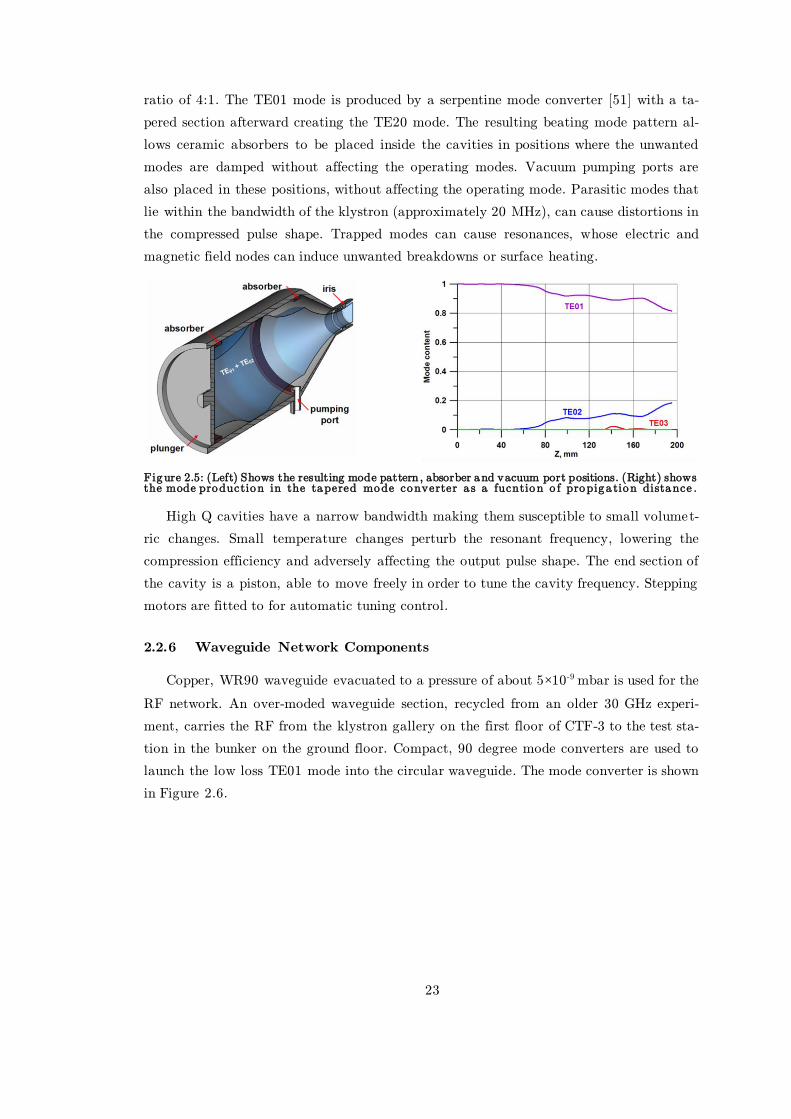
23
ratio of 4:1. The TE01 mode is produced by a serpentine mode converter [51] with a ta-
pered section afterward creating the TE20 mode. The resulting beating mode pattern al-
lows ceramic absorbers to be placed inside the cavities in positions where the unwanted
modes are damped without affecting the operating modes. Vacuum pumping ports are
also placed in these positions, without affecting the operating mode. Parasitic modes that
lie within the bandwidth of the klystron (approximately 20 MHz), can cause distortions in
the compressed pulse shape. Trapped modes can cause resonances, whose electric and
magnetic field nodes can induce unwanted breakdowns or surface heating.
Figure 2.5: (Left) Shows the resulting mode pattern , absorber and vacuum port positions. (Right) shows the mode production in the tapered mode converter a s a fucntion o f propiga tion distance .
High Q cavities have a narrow bandwidth making them susceptible to small volumet-
ric changes. Small temperature changes perturb the resonant frequency, lowering the
compression efficiency and adversely affecting the output pulse shape. The end section of
the cavity is a piston, able to move freely in order to tune the cavity frequency. Stepping
motors are fitted to for automatic tuning control.
2.2.6 Waveguide Network Components
Copper, WR90 waveguide evacuated to a pressure of about 5×10⁻⁹ mbar is used for the
RF network. An over-moded waveguide section, recycled from an older 30 GHz experi-
ment, carries the RF from the klystron gallery on the first floor of CTF-3 to the test sta-
tion in the bunker on the ground floor. Compact, 90 degree mode converters are used to
launch the low loss TE01 mode into the circular waveguide. The mode converter is shown
in Figure 2.6.
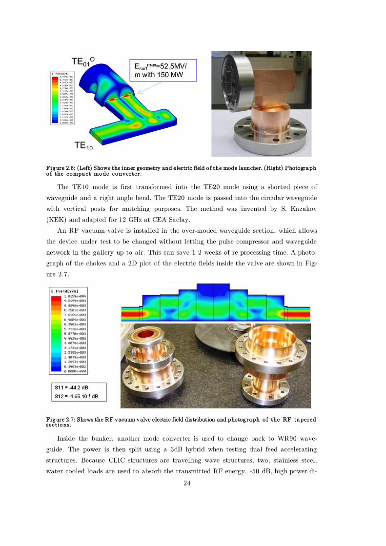
24
Figure 2.6: (Left) Shows the inner geometry and electric field o f the mode launcher. (Right) Photograph o f the compact mode converter.
The TE10 mode is first transformed into the TE20 mode using a shorted piece of
waveguide and a right angle bend. The TE20 mode is passed into the circular waveguide
with vertical posts for matching purposes. The method was invented by S. Kazakov
(KEK) and adapted for 12 GHz at CEA Saclay.
An RF vacuum valve is installed in the over-moded waveguide section, which allows
the device under test to be changed without letting the pulse compressor and waveguide
network in the gallery up to air. This can save 1-2 weeks of re-processing time. A photo-
graph of the chokes and a 2D plot of the electric fields inside the valve are shown in Fig-
ure 2.7.
Figure 2.7: Shows the RF vacuum valve electric field distribution and photog raph o f the RF tapered sections.
Inside the bunker, another mode converter is used to change back to WR90 wave-
guide. The power is then split using a 3dB hybrid when testing dual feed accelerating
structures. Because CLIC structures are travelling wave structures, two, stainless steel,
water cooled loads are used to absorb the transmitted RF energy. -50 dB, high power di-

25
rectional couplers are placed before and after the pulse compressor in the gallery and be-
fore and after the device under test in the bunker. The coupled signals are sent to the
LLRF system for acquisition and control using 50 ohm coaxial cables. Faraday cups are
placed in the upstream and downstream directions along the structure ’s beam axis to
measure dark current.
2.3 Test Stand Design: LLRF and Diagnostics
The LLRF (low level radio frequency) system has to produce a phase modulated si g-
nal for amplification by the TWT and klystron, acquire the RF signals from the direc-
tional couplers and acquire diagnostic signals from the structure and vacuum system. The
control system is made up of several different components including a PLC (Programma-
ble Logic Controller) based interlock system, VME (Versa Module Europa) crate based
arbitrary signal generation, OASIS PC based digitisers and a PXI (PCI eXtensions for
Instrumentation) based control system. The PLC was a standard Siemens unit. The VME
crate uses a VME bus and controller to link the operation of various expansion cards such
as voltage generators and digitizers. The PXI crate manufactured by National Instru-
ments [52] has a similar functionality to the VME crate but has a more modern standard.
2.3.1 Pulse forming network (PFN)
As described in sections 2.2.3 and 2.2.4, the pulse compressor requires a phase modu-
lated input pulse in order to produce a compressed, flat output pulse. There are several
components available on the market which can perform this task, such as IQ modulators,
PIN diodes, voltage controlled attenuators and voltage tuned phase shifters. Xbox-1 uses
the latter combination of a PIN diode, voltage tuned phase shifter and attenuator, con-
nected in series. Figure 2.8 shows a schematic diagram of the pulse forming network used
at Xbox-1.
Figure 2 .8 : Shows a schematic o f the pulse fo rming network fo r Xbox -1 .
An 11.9942 GHz CW signal is produced by an RF generator which is phase locked to
the master oscillator at CTF-3. The signal is split equally using a -3 dB hybrid coupler,
with half the power being sent to the local oscillator (LO) input of the IQ demodulation
crate and the other half to the PFN. The first component in the PFN is a 10-bit digital
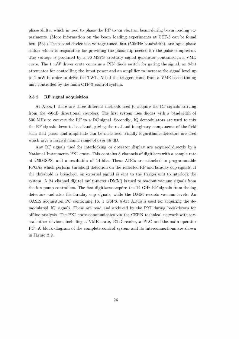
26
phase shifter which is used to phase the RF to an electron beam during beam loading ex-
periments. (More information on the beam loading experiments at CTF-3 can be found
here [53].) The second device is a voltage tuned, fast (50MHz bandwidth), analogue phase
shifter which is responsible for providing the phase flip needed for the pulse compressor.
The voltage is produced by a 96 MSPS arbitrary signal generator contained in a VME
crate. The 1 mW driver crate contains a PIN diode switch for gating the signal, an 8-bit
attenuator for controlling the input power and an amplifier to increase the signal level up
to 1 mW in order to drive the TWT. All of the triggers come from a VME based timing
unit controlled by the main CTF-3 control system.
2.3.2 RF signal acquisition
At Xbox-1 there are three different methods used to acquire the RF signals arriving
from the -50dB directional couplers. The first system uses diodes with a bandwidth of
500 MHz to convert the RF to a DC signal. Secondly, IQ demodulators are used to mix
the RF signals down to baseband, giving the real and imaginary components of the field
such that phase and amplitude can be measured. Finally logarithmic detectors are used
which give a large dynamic range of over 46 dB.
Any RF signals used for interlocking or operator display are acquired directly by a
National Instruments PXI crate. This contains 8 channels of digitisers with a sample rate
of 250MSPS, and a resolution of 14-bits. These ADCs are attached to programmable
FPGAs which perform threshold detection on the reflected RF and faraday cup signals. If
the threshold is breached, an external signal is sent to the trigger unit to interlock the
system. A 24 channel digital multi-meter (DMM) is used to readout vacuum signals from
the ion pump controllers. The fast digitizers acquire the 12 GHz RF signals from the log
detectors and also the faraday cup signals, while the DMM records vacuum levels. An
OASIS acquisition PC containing 16, 1 GSPS, 8-bit ADCs is used for acquiring the de-
modulated IQ signals. These are read and archived by the PXI during breakdowns for
offline analysis. The PXI crate communicates via the CERN technical network with sev-
eral other devices, including a VME crate, RTD reader, a PLC and the main operator
PC. A block diagram of the complete control system and its interconnections are shown
in Figure 2.9.
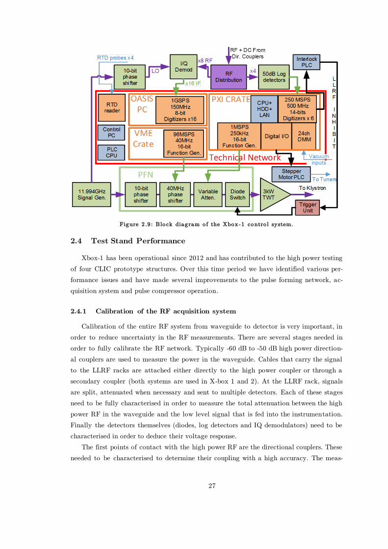
27
Figure 2 .9 : Blo ck diag ram o f the Xbox -1 contro l system.
2.4 Test Stand Performance
Xbox-1 has been operational since 2012 and has contributed to the high power testing
of four CLIC prototype structures. Over this time period we have identified various per-
formance issues and have made several improvements to the pulse forming network, ac-
quisition system and pulse compressor operation.
2.4.1 Calibration of the RF acquisition system
Calibration of the entire RF system from waveguide to detector is very important, in
order to reduce uncertainty in the RF measurements. There are several stages needed in
order to fully calibrate the RF network. Typically -60 dB to -50 dB high power direction-
al couplers are used to measure the power in the waveguide. Cables that carry the signal
to the LLRF racks are attached either directly to the high power coupler or through a
secondary coupler (both systems are used in X-box 1 and 2). At the LLRF rack, signals
are split, attenuated when necessary and sent to multiple detectors. Each of these stages
need to be fully characterised in order to measure the total attenuation between the high
power RF in the waveguide and the low level signal that is fed into the instrumentation.
Finally the detectors themselves (diodes, log detectors and IQ demodulators) need to be
characterised in order to deduce their voltage response.
The first points of contact with the high power RF are the directional couplers. These
needed to be characterised to determine their coupling with a high accuracy. The meas-
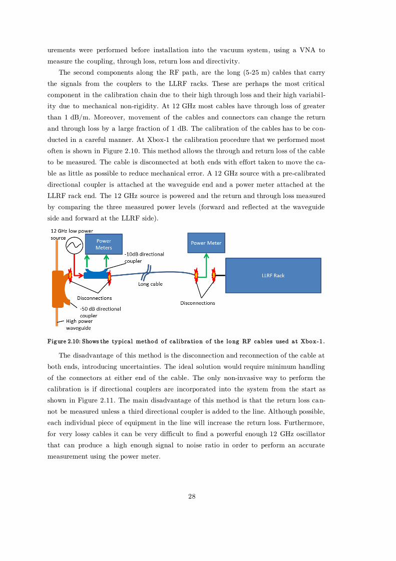
28
urements were performed before installation into the vacuum system, using a VNA to
measure the coupling, through loss, return loss and directivity.
The second components along the RF path, are the long (5-25 m) cables that carry
the signals from the couplers to the LLRF racks. These are perhaps the most critical
component in the calibration chain due to their high through loss and their high variabi l-
ity due to mechanical non-rigidity. At 12 GHz most cables have through loss of greater
than 1 dB/m. Moreover, movement of the cables and connectors can change the return
and through loss by a large fraction of 1 dB. The calibration of the cables has to be con-
ducted in a careful manner. At Xbox-1 the calibration procedure that we performed most
often is shown in Figure 2.10. This method allows the through and return loss of the cable
to be measured. The cable is disconnected at both ends with effort taken to move the ca-
ble as little as possible to reduce mechanical error. A 12 GHz source with a pre-calibrated
directional coupler is attached at the waveguide end and a power meter attached at the
LLRF rack end. The 12 GHz source is powered and the return and through loss measured
by comparing the three measured power levels (forward and reflected at the waveguide
side and forward at the LLRF side).
Figure 2.10: Shows the typica l method o f ca libra tion o f the long RF cables used a t Xbox-1 .
The disadvantage of this method is the disconnection and reconnection of the cable at
both ends, introducing uncertainties. The ideal solution would require minimum handling
of the connectors at either end of the cable. The only non-invasive way to perform the
calibration is if directional couplers are incorporated into the system from the start as
shown in Figure 2.11. The main disadvantage of this method is that the return loss can-
not be measured unless a third directional coupler is added to the line. Although possible,
each individual piece of equipment in the line will increase the return loss. Furthermore,
for very lossy cables it can be very difficult to find a powerful enough 12 GHz oscillator
that can produce a high enough signal to noise ratio in order to perform an accurate
measurement using the power meter.
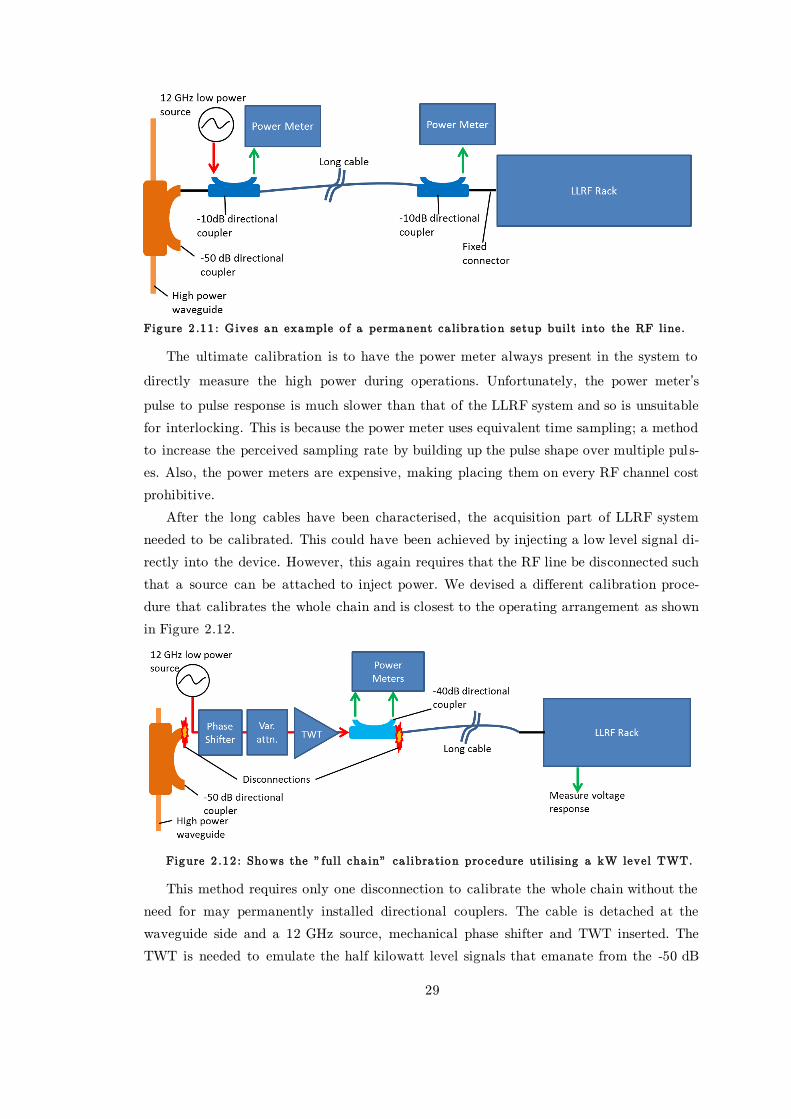
29
Figure 2 .11 : Gives an example o f a permanent ca libra tion setup built into the RF line.
The ultimate calibration is to have the power meter always present in the system to
directly measure the high power during operations. Unfortunately, the power meter’s
pulse to pulse response is much slower than that of the LLRF system and so is unsuitable
for interlocking. This is because the power meter uses equivalent time sampling; a method
to increase the perceived sampling rate by building up the pulse shape over multiple pul s-
es. Also, the power meters are expensive, making placing them on every RF channel cost
prohibitive.
After the long cables have been characterised, the acquisition part of LLRF system
needed to be calibrated. This could have been achieved by injecting a low level signal di-
rectly into the device. However, this again requires that the RF line be disconnected such
that a source can be attached to inject power. We devised a different calibration proce-
dure that calibrates the whole chain and is closest to the operating arrangement as shown
in Figure 2.12.
Figure 2 .12 : Shows the " full cha in" ca libra tion procedure utilising a kW level TWT.
This method requires only one disconnection to calibrate the whole chain without the
need for may permanently installed directional couplers. The cable is detached at the
waveguide side and a 12 GHz source, mechanical phase shifter and TWT inserted. The
TWT is needed to emulate the half kilowatt level signals that emanate from the -50 dB

30
couplers during normal high power operation. The voltage output of the LLRF detectors
is measured directly as the phase and amplitude are changed using the mechanical phase
shifter and variable attenuator.
Figure 2.13: Shows the calibration of the IQ demodulator performed using the TWT calibration method. The I and Q voltages are plotted on the complex plane (left) and the measured ang le shown (right).
Figure 2.13 gives an example of one of our calibrations that was performed using the
method described in Figure 2.12. Here the IQ demodulators have been calibrated by
sweeping the phase over 430 degrees at two different power levels. The data presented
show the IQ demodulator’s offset subtracted, but otherwise no other operations have been
made. A perfect IQ demodulator should produce a circular plot on the IQ diagram and
portray the same phase measurement behaviour at all power levels. The data on the IQ
diagram shows clear eccentricity and skew. The phase measurements in Figure 2.13
(right) show a clear offset and a different slope by > 4𝜎. The offset could be explained by
a cross correlation between the attenuation and phase behaviour of the variable attenua-
tor. However, the different slope can only be explained by a change in the behaviour of
the IQ demodulators. Over 360º the measurement error is more than 7º. Although unde-
sirable, the main purpose of phase measurements is to determine the position of break-
downs inside the DUT. This requires phase measurement accuracy only on the same order
of the typical phase advance per cell used in high gradient structures under test. This
typically ranges from 120º-150º.
2.4.2 Pulse forming network (PFN) Upgrade
The first iteration with respect to development of the PFN as described in section
2.3.1 contained an 8-bit digital attenuator to control the input power to the device under
test. This attenuator adjusted the power in steps of 0.25 dB. Communication to the de-
vice was conducted via the CERN network, by writing to a FESA class. This introduced
a large latency of 1.2 seconds. The control system used a very simple feedback loop in
order to adjust the power level to the desired set point. The attenuator input was in-

31
creased by steps of 6 codes every 1.2 seconds (due to the latency in the network). Once
the structure input power as measured by a log detector reached 75 % of the power set
point, the output was adjusted up or down by a single 8-bit increment, towards the de-
sired level. However, as shown in Figure 2.14 the granularity of the output power is ap-
proximately 0.5 MW. For breakdown rate studies this effect can be significant, due to the
strong power law dependence of the breakdown rate vs power [54].
Figure 2.14: Shows the mean flat-top power into the structure during a breakdown event and the subse-quent ramp back to full power. The 8 -bit a ttenua to r is used to contro l the power level.
We improved the resolution of the output power by replacing the 8-bit digital attenu-
ator with a Hittite voltage tuned attenuator. A control voltage was provided by an arbi-
trary signal generator with 16-bits of resolution contained in the PXI crate. Both the
measurement input (the log detector voltage as measured by a PXI digitiser) and the con-
trol output (PXI voltage generator) are contained in the PXI crate so communication be-
tween the devices can be fast.
Figure 2.15: Shows the mean flat-top power into the structure during a structure breakdown event and the subsequent ramp back to full power. The voltage tuned a ttenuator with 16 -bits of resolution is used, a long with the new PID contro l.
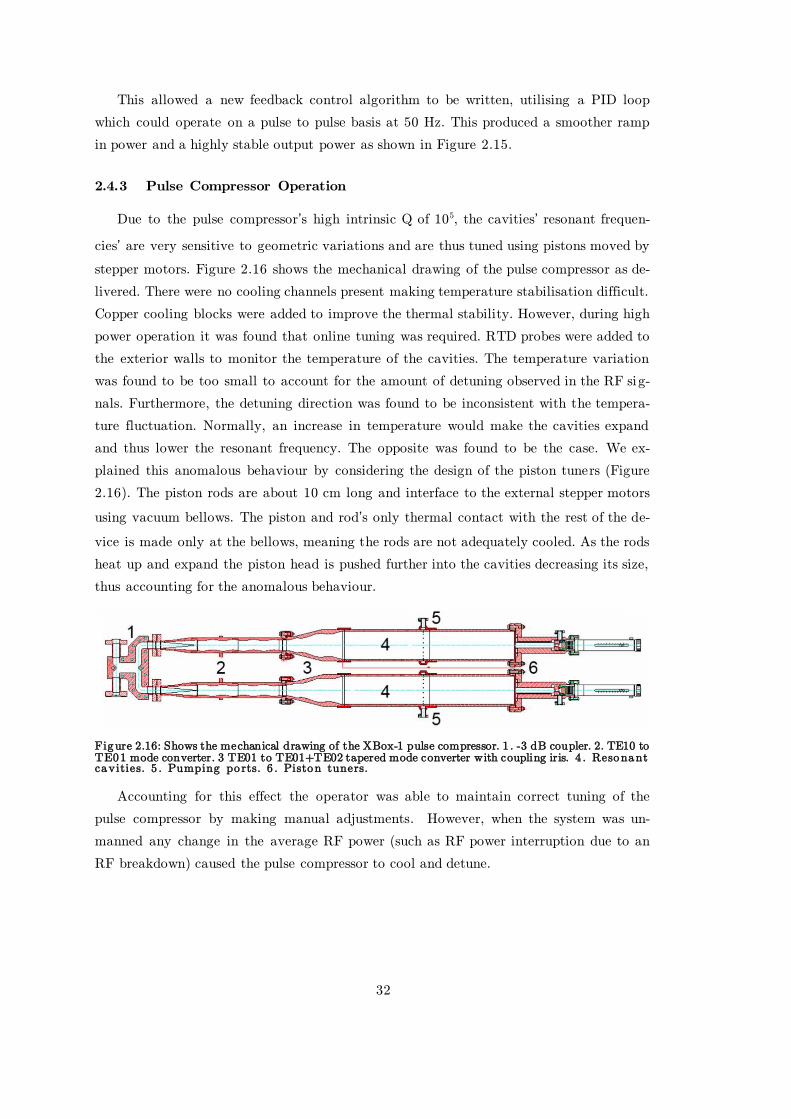
32
This allowed a new feedback control algorithm to be written, utilising a PID loop
which could operate on a pulse to pulse basis at 50 Hz. This produced a smoother ramp
in power and a highly stable output power as shown in Figure 2.15.
2.4.3 Pulse Compressor Operation
Due to the pulse compressor’s high intrinsic Q of 105, the cavities’ resonant frequen-
cies’ are very sensitive to geometric variations and are thus tuned using pistons moved by
stepper motors. Figure 2.16 shows the mechanical drawing of the pulse compressor as de-
livered. There were no cooling channels present making temperature stabilisation difficult.
Copper cooling blocks were added to improve the thermal stability. However, during high
power operation it was found that online tuning was required. RTD probes were added to
the exterior walls to monitor the temperature of the cavities. The temperature variation
was found to be too small to account for the amount of detuning observed in the RF sig-
nals. Furthermore, the detuning direction was found to be inconsistent with the tempera-
ture fluctuation. Normally, an increase in temperature would make the cavities expand
and thus lower the resonant frequency. The opposite was found to be the case. We ex-
plained this anomalous behaviour by considering the design of the piston tuners (Figure
2.16). The piston rods are about 10 cm long and interface to the external stepper motors
using vacuum bellows. The piston and rod’s only thermal contact with the rest of the de-
vice is made only at the bellows, meaning the rods are not adequately cooled. As the rods
heat up and expand the piston head is pushed further into the cavities decreasing its size,
thus accounting for the anomalous behaviour.
Figure 2.16: Shows the mechanical drawing of the XBox-1 pulse compressor. 1 . -3 dB coupler. 2. TE10 to TE01 mode converter. 3 TE01 to TE01+TE02 tapered mode converter with coupling iris. 4 . Resonant cavities. 5 . Pumping po rts. 6 . Piston tuners.
Accounting for this effect the operator was able to maintain correct tuning of the
pulse compressor by making manual adjustments. However, when the system was un-
manned any change in the average RF power (such as RF power interruption due to an
RF breakdown) caused the pulse compressor to cool and detune.
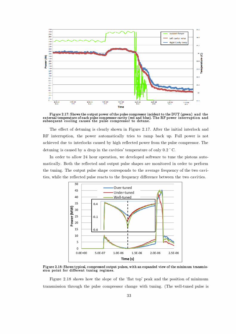
33
Figure 2.17: Shows the output power of the pulse compressor incident to the DUT (green) and the external temperature of each pulse compressor cavity (red and blue). The RF power interruption and subsequent coo ling causes the pulse compresso r to detune.
The effect of detuning is clearly shown in Figure 2.17. After the initial interlock and
RF interruption, the power automatically tries to ramp back up. Full power is not
achieved due to interlocks caused by high reflected power from the pulse compressor. The
detuning is caused by a drop in the cavities’ temperature of only 0.2ºC.
In order to allow 24 hour operation, we developed software to tune the pistons auto-
matically. Both the reflected and output pulse shapes are monitored in order to perform
the tuning. The output pulse shape corresponds to the average frequency of the two cavi-
ties, while the reflected pulse reacts to the frequency difference between the two cavities.
Figure 2.18: Shows typical, compressed output pulses, with an expanded view of the minimum transmis-sion po int fo r different tuning reg imes.
Figure 2.18 shows how the slope of the ‘flat top’ peak and the position of minimum
transmission through the pulse compressor change with tuning. (The well-tuned pulse is
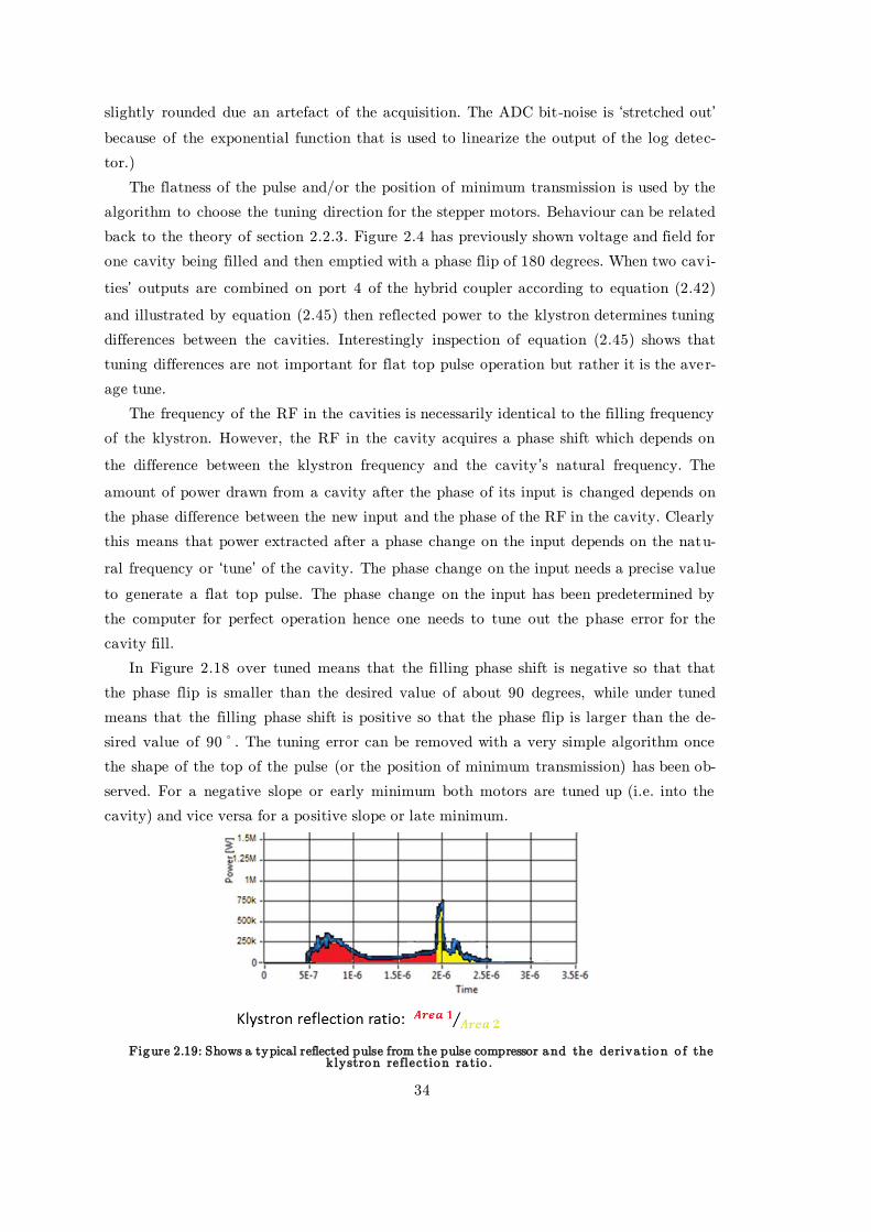
34
slightly rounded due an artefact of the acquisition. The ADC bit-noise is ‘stretched out’
because of the exponential function that is used to linearize the output of the log detec-
tor.)
The flatness of the pulse and/or the position of minimum transmission is used by the
algorithm to choose the tuning direction for the stepper motors. Behaviour can be related
back to the theory of section 2.2.3. Figure 2.4 has previously shown voltage and field for
one cavity being filled and then emptied with a phase flip of 180 degrees. When two cavi-
ties’ outputs are combined on port 4 of the hybrid coupler according to equation (2.42)
and illustrated by equation (2.45) then reflected power to the klystron determines tuning
differences between the cavities. Interestingly inspection of equation (2.45) shows that
tuning differences are not important for flat top pulse operation but rather it is the aver-
age tune.
The frequency of the RF in the cavities is necessarily identical to the filling frequency
of the klystron. However, the RF in the cavity acquires a phase shift which depends on
the difference between the klystron frequency and the cavity ’s natural frequency. The
amount of power drawn from a cavity after the phase of its input is changed depends on
the phase difference between the new input and the phase of the RF in the cavity. Clearly
this means that power extracted after a phase change on the input depends on the natu-
ral frequency or ‘tune’ of the cavity. The phase change on the input needs a precise value
to generate a flat top pulse. The phase change on the input has been predetermined by
the computer for perfect operation hence one needs to tune out the phase error for the
cavity fill.
In Figure 2.18 over tuned means that the filling phase shift is negative so that that
the phase flip is smaller than the desired value of about 90 degrees, while under tuned
means that the filling phase shift is positive so that the phase flip is larger than the de-
sired value of 90º. The tuning error can be removed with a very simple algorithm once
the shape of the top of the pulse (or the position of minimum transmission) has been ob-
served. For a negative slope or early minimum both motors are tuned up (i.e. into the
cavity) and vice versa for a positive slope or late minimum.
Figure 2.19: Shows a typical reflected pulse from the pulse compressor and the deriva tion o f the klystron reflection ra tio .
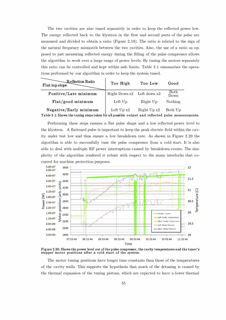
35
The two cavities are also tuned separately in order to keep the reflected power low.
The energy reflected back to the klystron in the first and second parts of the pulse are
measured and divided to obtain a ratio (Figure 2.19). The ratio is related to the sign of
the natural frequency mismatch between the two cavities. Also, the use of a ratio as op-
posed to just measuring reflected energy during the filling of the pulse compressor allows
the algorithm to work over a large range of power levels. By tuning the motors separately
this ratio can be controlled and kept within safe limits. Table 2.1 summarises the opera-
tions performed by our algorithm in order to keep the system tuned.
Reflection Ratio Flat top slope
Too High Too Low Good
Positive/Late minimum Right Down x2 Left down x2 Both Down
Flat/good minimum Left Up Right Up Nothing
Negative/Early minimum Left Up x2 Right Up x2 Both Up
Table 2 .1: Shows the tuning steps taken for a ll possible output and reflected pulse measurements.
Performing these steps ensures a flat pulse shape and a low reflected power level to
the klystron. A flattened pulse is important to keep the peak electric field within the cav-
ity under test low and thus ensure a low breakdown rate. As shown in Figure 2.20 the
algorithm is able to successfully tune the pulse compressor from a cold start. It is also
able to deal with multiple RF power interruptions caused by breakdown events. The sim-
plicity of the algorithm rendered it robust with respect to the many interlocks that oc-
curred for machine protection purposes.
Figure 2.20: Shows the power level out of the pulse compressor, the cavity temperatures and the tuner's stepper moto r po sitions a fter a co ld sta rt o f the system.
The motor tuning positions have longer time constants than those of the temperatures
of the cavity walls. This supports the hypothesis that much of the detuning is caused by
the thermal expansion of the tuning pistons, which are expected to have a lower thermal

36
conductivity and thus transfer their heat energy more slowly. Due to the implementation
of the algorithm the test stand can run 24 hours a day and can recover from severe
breakdown clusters. The introduction of our control algorithm contributed a huge step in
the productivity of the test stand.
2.4.4 Structure Conditioning Algorithm
As described in section 1.6, RF structures need to be conditioned over time by in-
creasing the input power level and pulse width. Usually this operation is performed by a
machine operator by looking at the vacuum level or breakdown rate (BDR) inside the
structure. However, this approach is open to interpretation and human error. In the worst
cases this can result in large increases in power and pulse width, thus increasing the
chances of damage or degradation to the structure’s performance. It can also be difficult
to perform or agree on a well-defined strategy for conditioning structures. Any quantitate
comparison between structures tested at different places and at different times becomes
difficult. Some of the problems are shown in the Figure 2.21.
Figure 2.21: Shows the input power (green) and accumulated number o f breakdowns (bla ck) in a T24 CLIC structure during conditioning a t Xbox -1 . Power was contro lled by the opera to r.
Figure 2.21 shows some of the processing that was performed at Xbox-1 on a T24
CLIC accelerating structure. It shows 37 million pulses equivalent to 8.5 days of RF on
time. The gradient of the black line (accumulated number of breakdowns) is not constant,
meaning the BDR is changing. The rate of power increase is sporadic which can have an
adverse effect on structure performance. These effects are observed because the test stand
was running 24 hours per day but only under operator supervision for 8 hours per day.
The operator would change the power level depending on the observed BDR. If the BDR
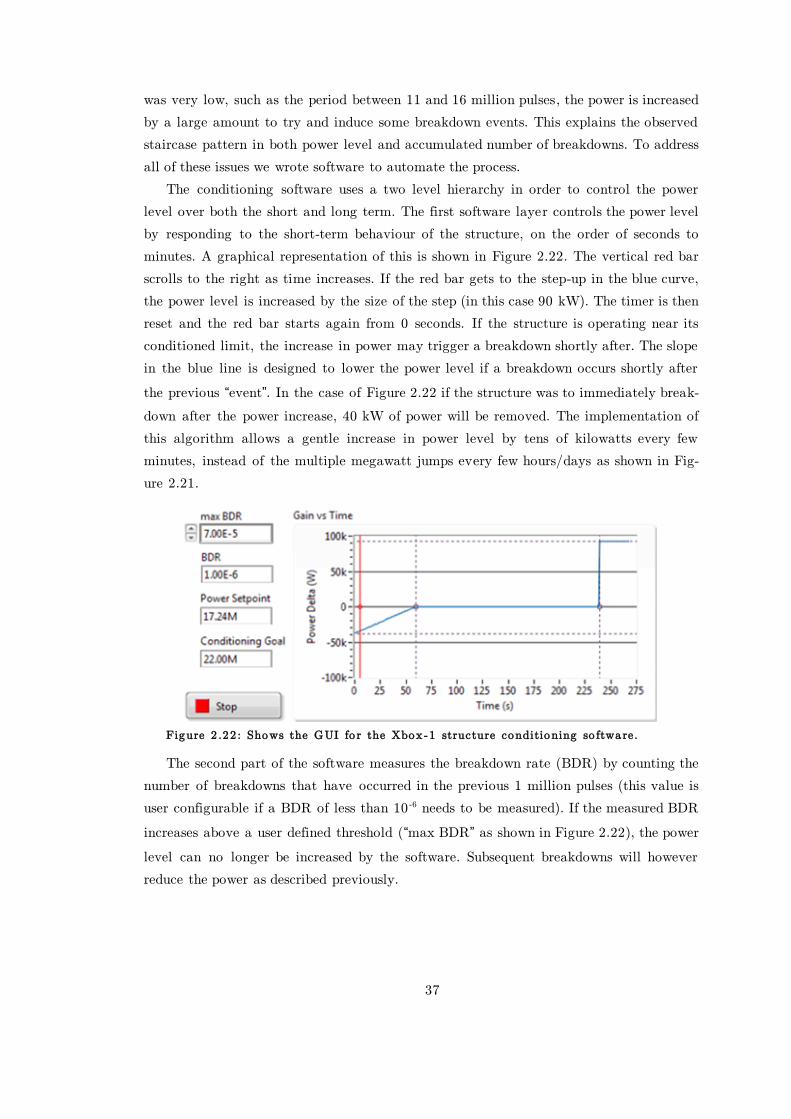
37
was very low, such as the period between 11 and 16 million pulses, the power is increased
by a large amount to try and induce some breakdown events. This explains the observed
staircase pattern in both power level and accumulated number of breakdowns. To address
all of these issues we wrote software to automate the process.
The conditioning software uses a two level hierarchy in order to control the power
level over both the short and long term. The first software layer controls the power level
by responding to the short-term behaviour of the structure, on the order of seconds to
minutes. A graphical representation of this is shown in Figure 2.22. The vertical red bar
scrolls to the right as time increases. If the red bar gets to the step-up in the blue curve,
the power level is increased by the size of the step (in this case 90 kW). The timer is then
reset and the red bar starts again from 0 seconds. If the structure is operating near its
conditioned limit, the increase in power may trigger a breakdown shortly after. The slope
in the blue line is designed to lower the power level if a breakdown occurs shortly after
the previous “event”. In the case of Figure 2.22 if the structure was to immediately break-
down after the power increase, 40 kW of power will be removed. The implementation of
this algorithm allows a gentle increase in power level by tens of kilowatts every few
minutes, instead of the multiple megawatt jumps every few hours/days as shown in Fig-
ure 2.21.
Figure 2 .22 : Shows the GUI fo r the Xbox -1 structure conditioning so ftware.
The second part of the software measures the breakdown rate (BDR) by counting the
number of breakdowns that have occurred in the previous 1 million pulses (this value is
user configurable if a BDR of less than 10 -6 needs to be measured). If the measured BDR
increases above a user defined threshold (“max BDR” as shown in Figure 2.22), the power
level can no longer be increased by the software. Subsequent breakdowns will however
reduce the power as described previously.

38
Figure 2.23: Shows the power increase into a T24 CLIC prototype accelerating structure as a func-tion o f the number of pulses (green). Also shown in red a re the a ccumulated number o f breakdowns.
As shown in Figure 2.23, after the conditioning software is activated the BDR remains
constant, i.e. the accumulated number of breakdowns is a straight line. The conditioning
software was set to produce a BDR of 7×10⁻⁵, while the calculated result from Figure 2.23
is 7.8×10⁻⁵ for the 3.4 million pulses that the software was active. This is a very good re-
sult, considering that the BDR varied by more than two orders of magnitude when the
algorithm was not used, such as in Figure 2.21. Use of the conditioning algorithm is now
standard practice at all of CERN’s high power test stands and has been very successful in
conditioning structures and waveguide networks up to high gradients. The results will be
discussed in further detail in later chapters.
2.5 Conclusion
Standalone test stands allow for the testing and verification of various high power RF
components, including prototype accelerating structures. They provide a test-bed for de-
velopment of control and LLRF systems. The design and layout of CERN’s first
standalone X-band test stand has been presented. The importance of each component has
been outlined and explored, with detailed discussions about state of the art X-band klys-
trons and pulse compressors explored. The LLRF system including the PFN, RF acquisi-
tion and interlock systems have been outlined. Several performance issues have been iden-
tified, such as calibration procedures, output power resolution, pulse compressor stability
and structure conditioning strategies. Solutions to the problems were found and the rel e-
vant software and hardware changes were made.
The upgrades to Xbox-1 have resulted in the test stand running reliably for over a
year and the successful testing of two CLIC prototype accelerating structures. Significant

39
progress has been made in understanding how to commission and run an X-band high
power test stand. The lessons learned have been applied to the design of the second,
standalone test stand at CERN; Xbox-2. The design and commissioning of Xbox-2 will be
discussed in detail in Chapter 3.
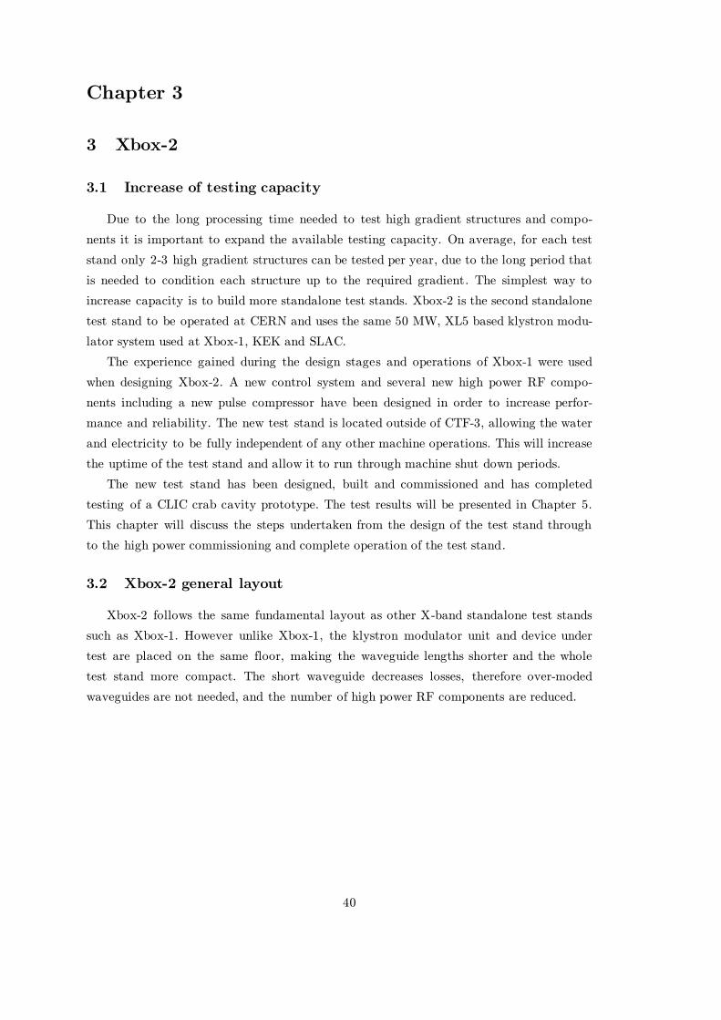
40
Chapter 3
3 Xbox-2
3.1 Increase of testing capacity
Due to the long processing time needed to test high gradient structures and compo-
nents it is important to expand the available testing capacity. On average, for each test
stand only 2-3 high gradient structures can be tested per year, due to the long period that
is needed to condition each structure up to the required gradient. The simplest way to
increase capacity is to build more standalone test stands. Xbox-2 is the second standalone
test stand to be operated at CERN and uses the same 50 MW, XL5 based klystron modu-
lator system used at Xbox-1, KEK and SLAC.
The experience gained during the design stages and operations of Xbox-1 were used
when designing Xbox-2. A new control system and several new high power RF compo-
nents including a new pulse compressor have been designed in order to increase perfor-
mance and reliability. The new test stand is located outside of CTF-3, allowing the water
and electricity to be fully independent of any other machine operations. This will increase
the uptime of the test stand and allow it to run through machine shut down periods.
The new test stand has been designed, built and commissioned and has completed
testing of a CLIC crab cavity prototype. The test results will be presented in Chapter 5.
This chapter will discuss the steps undertaken from the design of the test stand through
to the high power commissioning and complete operation of the test stand.
3.2 Xbox-2 general layout
Xbox-2 follows the same fundamental layout as other X-band standalone test stands
such as Xbox-1. However unlike Xbox-1, the klystron modulator unit and device under
test are placed on the same floor, making the waveguide lengths shorter and the whole
test stand more compact. The short waveguide decreases losses, therefore over-moded
waveguides are not needed, and the number of high power RF components are reduced.
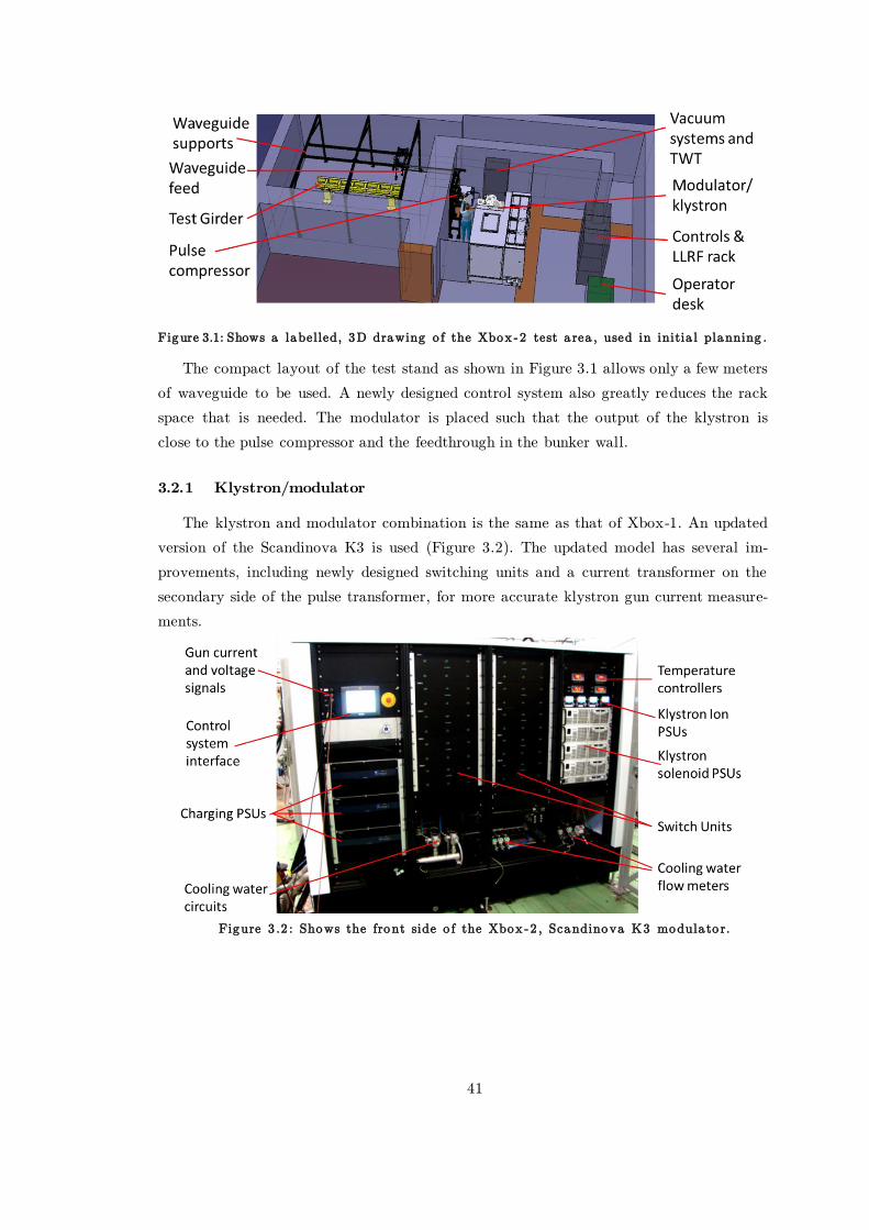
41
Figure 3.1: Shows a labelled, 3D drawing o f the Xbox -2 test a rea , used in initia l planning .
The compact layout of the test stand as shown in Figure 3.1 allows only a few meters
of waveguide to be used. A newly designed control system also greatly reduces the rack
space that is needed. The modulator is placed such that the output of the klystron is
close to the pulse compressor and the feedthrough in the bunker wall.
3.2.1 Klystron/modulator
The klystron and modulator combination is the same as that of Xbox-1. An updated
version of the Scandinova K3 is used (Figure 3.2). The updated model has several im-
provements, including newly designed switching units and a current transformer on the
secondary side of the pulse transformer, for more accurate klystron gun current measure-
ments.
Figure 3 .2 : Shows the front side o f the Xbox -2 , Scandinova K3 modula to r.

42
Figure 3.3: Shows a photograph of the XL5 klystron installed into the rea r right hand co rner o f the
Xbox-2 modula to r, a s viewed from the perspective shown in Figure 3 .2 .
3.2.2 Pulse Compressor and Waveguide components
A new pulse compressor has been designed for Xbox-2 in order to improve the reliabil-
ity and ease of operation. It is a SLED-I type pulse compressor, which can obtain a peak
power compression ratio of 3, when compressing the 1.5 𝜇s klystron pulse to a 250 ns out-
put pulse. The RF design, cold testing and tuning of the device will be explored in further
detail in section 3.4.
Figure 3 .4 : Shows the pulse compresso r and surrounding waveguide components.
Figure 3.4 shows the pulse compressor and several of the new waveguide components.
New RF gate valves, waveguide vacuum ports, hybrids and directional couplers are used
for the first time on the test stand. All of these components were successfully cold tested
before installation.
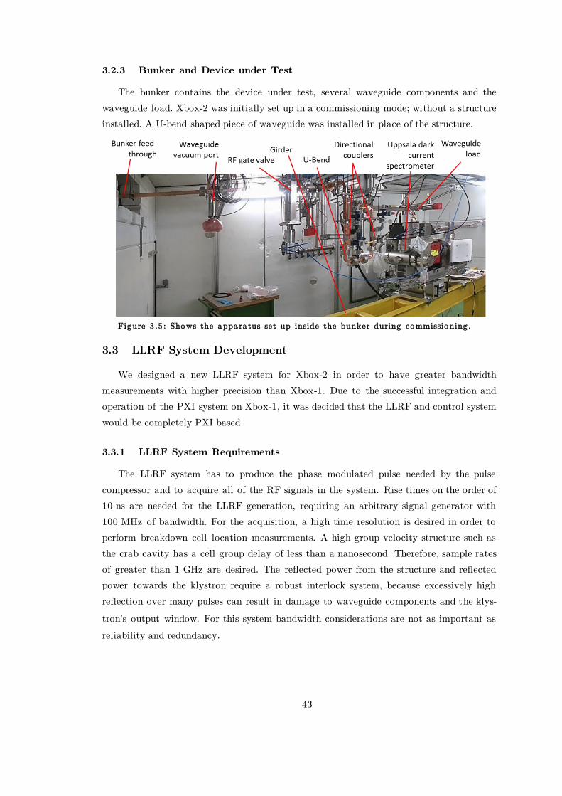
43
3.2.3 Bunker and Device under Test
The bunker contains the device under test, several waveguide components and the
waveguide load. Xbox-2 was initially set up in a commissioning mode; without a structure
installed. A U-bend shaped piece of waveguide was installed in place of the structure.
Figure 3 .5 : Shows the appara tus set up inside the bunker during commissioning .
3.3 LLRF System Development
We designed a new LLRF system for Xbox-2 in order to have greater bandwidth
measurements with higher precision than Xbox-1. Due to the successful integration and
operation of the PXI system on Xbox-1, it was decided that the LLRF and control system
would be completely PXI based.
3.3.1 LLRF System Requirements
The LLRF system has to produce the phase modulated pulse needed by the pulse
compressor and to acquire all of the RF signals in the system. Rise times on the order of
10 ns are needed for the LLRF generation, requiring an arbitrary signal generator with
100 MHz of bandwidth. For the acquisition, a high time resolution is desired in order to
perform breakdown cell location measurements. A high group velocity structure such as
the crab cavity has a cell group delay of less than a nanosecond. Therefore, sample rates
of greater than 1 GHz are desired. The reflected power from the structure and reflected
power towards the klystron require a robust interlock system, because excessively high
reflection over many pulses can result in damage to waveguide components and the klys-
tron’s output window. For this system bandwidth considerations are not as important as
reliability and redundancy.

44
3.3.2 LLRF System PXI Hardware
The generation and acquisition bandwidth requirements set the minimum IFs (inter-
mediate frequencies) that are needed when up and down mixing. In turn this dictates the
digitization and signal generation bandwidths and thus the hardware specifications. With
the added restriction of using PXI based hardware which is compatible with the FPGA
interlocking used on Xbox-1, the range of hardware available on the market is quite
small. For digitisation, two cards are available: the NI 5771 and NI 5772. Both utilise the
required FPGA interface but have different sample rates and resolutions. The NI 5771 has
a sample rate of 3 GS/s and a resolution of 8-bits, while the NI 5772 has a sample rate of
1.6 GS/s and 12-bits of resolution. It was decided to use the NI 5772 due to its high reso-
lution. The NI 5771’s 8-bits of resolution would result in a smaller measurement accuracy
and dynamic range. The increased sample rate is not needed as there is no plan to test
structures with cell group delays of less than 0.625 ns.
The function of the data acquisition is to accurately determine the amplitude and
phase of a 12 GHz signal. Currently, it is not practical to directly sample a 12 GHz signal
hence it must be mixed to a much lower frequency where direct sampling is possible with
commercial hardware. Mixing preserves amplitude and phase. The frequency to which we
mix to is the IF.
The ADC in the NI 5772 has an analogue bandwidth of 800 MHz. We note that with
this bandwidth one can still just time resolve rising/falling edges separated by 0.625 ns by
virtue of the fact that filtering at this bandwidth does not completely remove features at
the associated timescale. The IF needs to be below 800 MHz to avoid aliasing of the ac-
quired signal; it also needs to be high so that it resolves fast changes. In order to see all
features in the available 800 MHz bandwidth admitted by the ADC, one has to choose an
IF of 400 MHz. The digitisers used, sample at a frequency of 1.6 GS/s resulting in 4-times
oversampling. Digital sampling gives instantaneous voltages rather than amplitude and
phase. It is natural to process these acquired voltages using the in-phase 𝐼 and quadrature
𝑄 components. One defines 𝐼 and 𝑄 components and relates them to the measured voltage
𝑉𝑚 , amplitude 𝐴 and phase 𝜑 using the equation:
𝑉𝑚(𝑡) = 𝐴𝑐𝑜𝑠(𝜔𝑡 + 𝑛𝜑) = 𝑅𝑒{(𝐼 + 𝑗𝑄)𝑒𝑗𝜔𝑡} (3.1)
The signal is sampled at times 𝑡𝑛 = 𝑛∅𝜔⁄ where 𝑛 = 0,1,2… and ∅ is the phase angle
between samples, hence
𝑉𝑚(𝑡𝑛) = 𝑅𝑒{(𝐼 + 𝑗𝑄)𝑒𝑗𝑛∅} (3.2)
For this case where the sample rate is 1.6 GHz and the sampled frequency is
400 MHz, ∅ is 90 degrees. An angle of 90 degrees presents a special case where for equa-
tion (3.2), the samples read out as I, -Q, -I and Q, in a cyclical fashion. This means that no
trigonometry needs to be conducted by the algorithm and it can be performed with very
little computing power. This operation is ideally suited to being conducted on an FPGA.
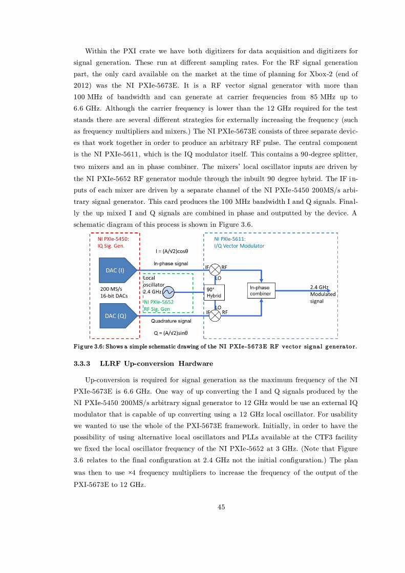
45
Within the PXI crate we have both digitizers for data acquisition and digiti zers for
signal generation. These run at different sampling rates. For the RF signal generation
part, the only card available on the market at the time of planning for Xbox-2 (end of
2012) was the NI PXIe-5673E. It is a RF vector signal generator with more than
100 MHz of bandwidth and can generate at carrier frequencies from 85 MHz up to
6.6 GHz. Although the carrier frequency is lower than the 12 GHz required for the test
stands there are several different strategies for externally increasing the frequency (such
as frequency multipliers and mixers.) The NI PXIe-5673E consists of three separate devic-
es that work together in order to produce an arbitrary RF pulse. The central component
is the NI PXIe-5611, which is the IQ modulator itself. This contains a 90-degree splitter,
two mixers and an in phase combiner. The mixers’ local oscillator inputs are driven by
the NI PXIe-5652 RF generator module through the inbuilt 90 degree hybrid. The IF in-
puts of each mixer are driven by a separate channel of the NI PXIe-5450 200MS/s arbi-
trary signal generator. This card produces the 100 MHz bandwidth I and Q signals. Final-
ly the up mixed I and Q signals are combined in phase and outputted by the device. A
schematic diagram of this process is shown in Figure 3.6.
Figure 3.6: Shows a simple schematic drawing of the NI PXIe -5673E RF vecto r signa l g enera to r.
3.3.3 LLRF Up-conversion Hardware
Up-conversion is required for signal generation as the maximum frequency of the NI
PXIe-5673E is 6.6 GHz. One way of up converting the I and Q signals produced by the
NI PXIe-5450 200MS/s arbitrary signal generator to 12 GHz would be use an external IQ
modulator that is capable of up converting using a 12 GHz local oscillator. For usability
we wanted to use the whole of the PXI-5673E framework. Initially, in order to have the
possibility of using alternative local oscillators and PLLs available at the CTF3 facility
we fixed the local oscillator frequency of the NI PXIe-5652 at 3 GHz. (Note that Figure
3.6 relates to the final configuration at 2.4 GHz not the initial configuration.) The plan
was then to use ×4 frequency multipliers to increase the frequency of the output of the
PXI-5673E to 12 GHz.
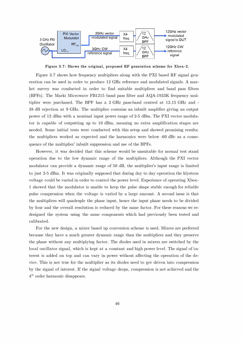
46
Figure 3 .7 : Shows the o rig ina l , propo sed RF genera tion scheme fo r Xbox -2 .
Figure 3.7 shows how frequency multipliers along with the PXI based RF signal gen-
eration can be used in order to produce 12 GHz reference and modulated signals. A mar-
ket survey was conducted in order to find suitable multipliers and band pass filters
(BPFs). The Marki Microwave FB1215 band pass filter and AQA-1933K frequency mul-
tiplier were purchased. The BPF has a 2 GHz pass-band centred at 12.15 GHz and -
38 dB rejection at 9 GHz. The multiplier contains an inbuilt amplifier giving an output
power of 12 dBm with a nominal input power range of 2-5 dBm. The PXI vector modula-
tor is capable of outputting up to 10 dBm, meaning no extra amplification stages are
needed. Some initial tests were conducted with this setup and showed promising results;
the multipliers worked as expected and the harmonics were below -60 dBc as a conse-
quence of the multiplier’ inbuilt suppression and use of the BPFs.
However, it was decided that this scheme would be unsuitable for normal test stand
operation due to the low dynamic range of the multipliers. Although the PXI vector
modulator can provide a dynamic range of 50 dB, the multiplier’s input range is limited
to just 2-5 dBm. It was originally supposed that during day to day operation the klystron
voltage could be varied in order to control the power level. Experience of operating Xbox-
1 showed that the modulator is unable to keep the pulse shape stable enough for reliable
pulse compression when the voltage is varied by a large amount. A second issue is that
the multipliers will quadruple the phase input, hence the input phase needs to be divided
by four and the overall resolution is reduced by the same factor. For these reasons we re-
designed the system using the same components which had previously been tested and
calibrated.
For the new design, a mixer based up conversion scheme is used. Mixers are preferred
because they have a much greater dynamic range than the multipliers and they preserve
the phase without any multiplying factor. The diodes used in mixers are switched by the
local oscillator signal, which is kept at a constant and high power level. The signal of i n-
terest is added on top and can vary in power without affecting the operation of the de-
vice. This is not true for the multiplier as its diodes need to get driven into compression
by the signal of interest. If the signal voltage drops, compression is not achieved and the
4th order harmonic disappears.
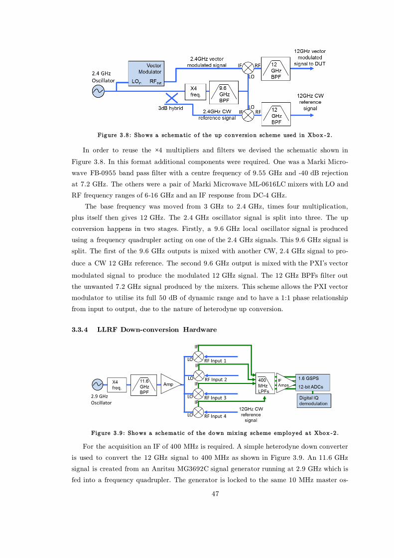
47
Figure 3 .8 : Shows a schematic o f the up conversion scheme used in Xbox -2 .
In order to reuse the ×4 multipliers and filters we devised the schematic shown in
Figure 3.8. In this format additional components were required. One was a Marki Micro-
wave FB-0955 band pass filter with a centre frequency of 9.55 GHz and -40 dB rejection
at 7.2 GHz. The others were a pair of Marki Microwave ML-0616LC mixers with LO and
RF frequency ranges of 6-16 GHz and an IF response from DC-4 GHz.
The base frequency was moved from 3 GHz to 2.4 GHz, times four multiplication,
plus itself then gives 12 GHz. The 2.4 GHz oscillator signal is split into three. The up
conversion happens in two stages. Firstly, a 9.6 GHz local oscillator signal is produced
using a frequency quadrupler acting on one of the 2.4 GHz signals. This 9.6 GHz signal is
split. The first of the 9.6 GHz outputs is mixed with another CW, 2.4 GHz signal to pro-
duce a CW 12 GHz reference. The second 9.6 GHz output is mixed with the PXI’s vector
modulated signal to produce the modulated 12 GHz signal. The 12 GHz BPFs filter out
the unwanted 7.2 GHz signal produced by the mixers. This scheme allows the PXI vector
modulator to utilise its full 50 dB of dynamic range and to have a 1:1 phase relationship
from input to output, due to the nature of heterodyne up conversion.
3.3.4 LLRF Down-conversion Hardware
Figure 3 .9 : Shows a schematic o f the down mixing scheme employed a t Xbox -2 .
For the acquisition an IF of 400 MHz is required. A simple heterodyne down converter
is used to convert the 12 GHz signal to 400 MHz as shown in Figure 3.9. An 11.6 GHz
signal is created from an Anritsu MG3692C signal generator running at 2.9 GHz which is
fed into a frequency quadrupler. The generator is locked to the same 10 MHz master os-
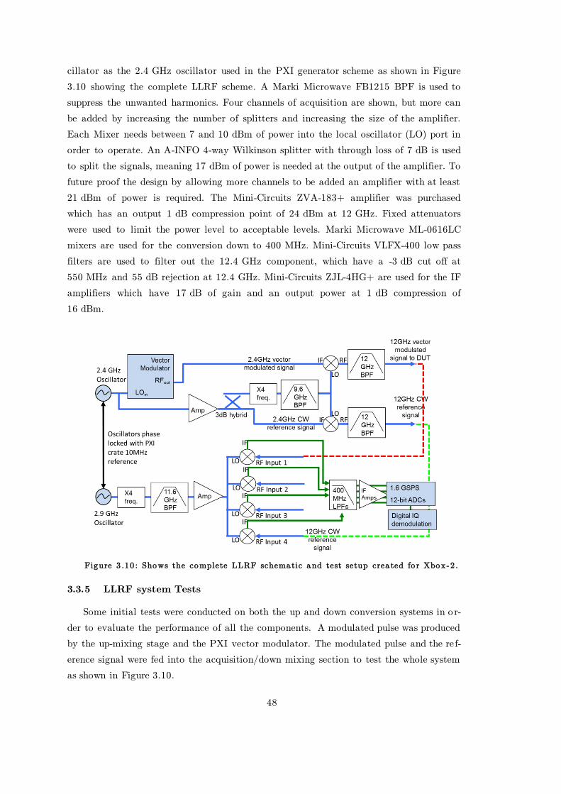
48
cillator as the 2.4 GHz oscillator used in the PXI generator scheme as shown in Figure
3.10 showing the complete LLRF scheme. A Marki Microwave FB1215 BPF is used to
suppress the unwanted harmonics. Four channels of acquisition are shown, but more can
be added by increasing the number of splitters and increasing the size of the amplifier.
Each Mixer needs between 7 and 10 dBm of power into the local oscillator (LO) port in
order to operate. An A-INFO 4-way Wilkinson splitter with through loss of 7 dB is used
to split the signals, meaning 17 dBm of power is needed at the output of the amplifier. To
future proof the design by allowing more channels to be added an amplifier with at least
21 dBm of power is required. The Mini-Circuits ZVA-183+ amplifier was purchased
which has an output 1 dB compression point of 24 dBm at 12 GHz. Fixed attenuators
were used to limit the power level to acceptable levels. Marki Microwave ML-0616LC
mixers are used for the conversion down to 400 MHz. Mini-Circuits VLFX-400 low pass
filters are used to filter out the 12.4 GHz component, which have a -3 dB cut off at
550 MHz and 55 dB rejection at 12.4 GHz. Mini-Circuits ZJL-4HG+ are used for the IF
amplifiers which have 17 dB of gain and an output power at 1 dB compression of
16 dBm.
Figure 3 .10 : Shows the complete LLRF schematic and test setup crea ted fo r Xbox -2 .
3.3.5 LLRF system Tests
Some initial tests were conducted on both the up and down conversion systems in o r-
der to evaluate the performance of all the components. A modulated pulse was produced
by the up-mixing stage and the PXI vector modulator. The modulated pulse and the ref-
erence signal were fed into the acquisition/down mixing section to test the whole system
as shown in Figure 3.10.
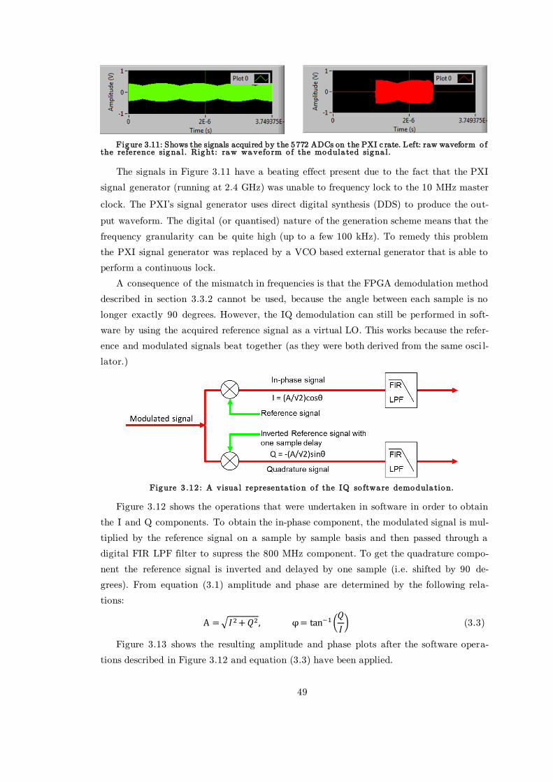
49
Figure 3.11: Shows the signals acquired by the 5772 ADCs on the PXI c rate. Left: raw waveform o f the reference signa l. Right: raw wavefo rm o f the modula ted signa l.
The signals in Figure 3.11 have a beating effect present due to the fact that the PXI
signal generator (running at 2.4 GHz) was unable to frequency lock to the 10 MHz master
clock. The PXI’s signal generator uses direct digital synthesis (DDS) to produce the out-
put waveform. The digital (or quantised) nature of the generation scheme means that the
frequency granularity can be quite high (up to a few 100 kHz). To remedy this problem
the PXI signal generator was replaced by a VCO based external generator that is able to
perform a continuous lock.
A consequence of the mismatch in frequencies is that the FPGA demodulation method
described in section 3.3.2 cannot be used, because the angle between each sample is no
longer exactly 90 degrees. However, the IQ demodulation can still be performed in soft-
ware by using the acquired reference signal as a virtual LO. This works because the refer-
ence and modulated signals beat together (as they were both derived from the same osci l-
lator.)
Figure 3 .12 : A visua l representa tion o f the IQ so ftware demodula tion.
Figure 3.12 shows the operations that were undertaken in software in order to obtain
the I and Q components. To obtain the in-phase component, the modulated signal is mul-
tiplied by the reference signal on a sample by sample basis and then passed through a
digital FIR LPF filter to supress the 800 MHz component. To get the quadrature compo-
nent the reference signal is inverted and delayed by one sample (i.e. shifted by 90 de-
grees). From equation (3.1) amplitude and phase are determined by the following rela-
tions:
A = √𝐼2+ 𝑄2 , φ= tan−1(𝑄
𝐼) (3.3)
Figure 3.13 shows the resulting amplitude and phase plots after the software opera-
tions described in Figure 3.12 and equation (3.3) have been applied.
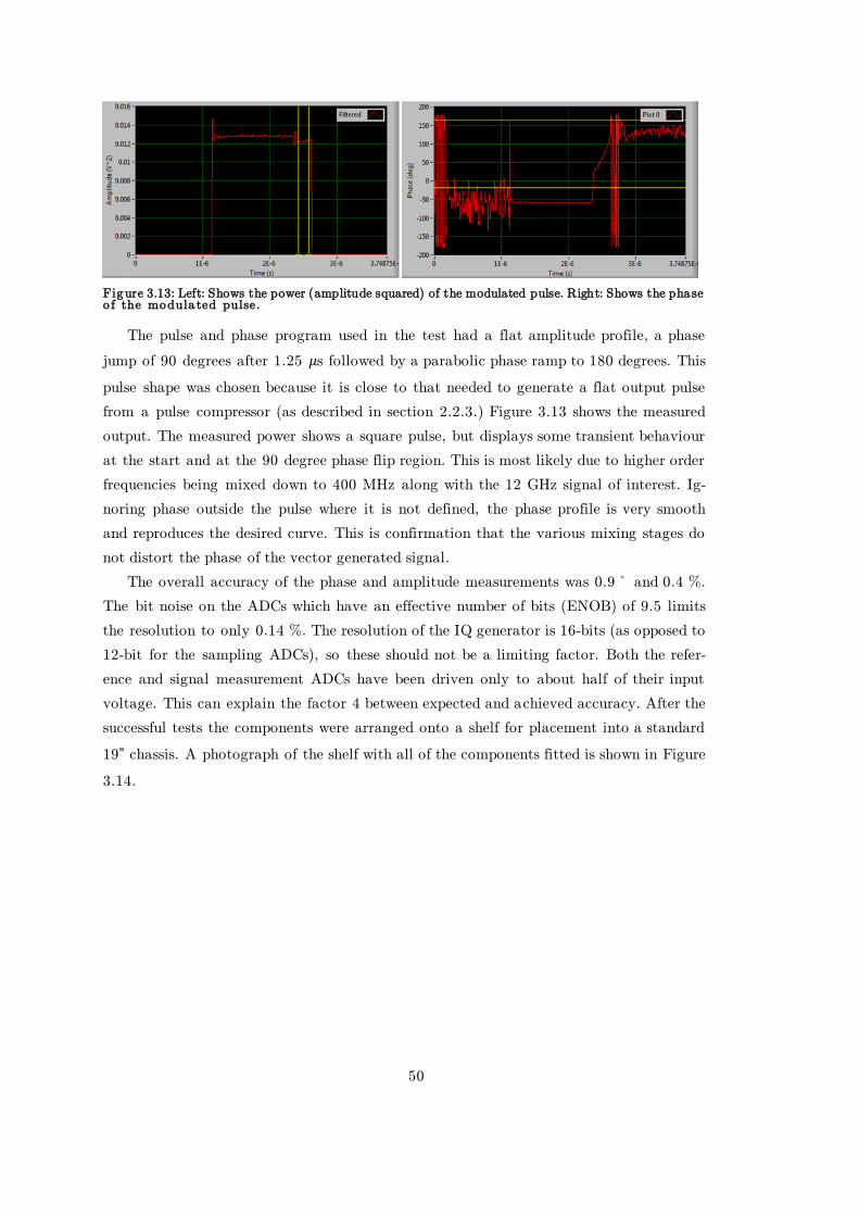
50
Figure 3.13: Left: Shows the power (amplitude squared) of the modulated pulse. Right: Shows the phase o f the modula ted pulse.
The pulse and phase program used in the test had a flat amplitude profile, a phase
jump of 90 degrees after 1.25 𝜇s followed by a parabolic phase ramp to 180 degrees. This
pulse shape was chosen because it is close to that needed to generate a flat output pulse
from a pulse compressor (as described in section 2.2.3.) Figure 3.13 shows the measured
output. The measured power shows a square pulse, but displays some transient behaviour
at the start and at the 90 degree phase flip region. This is most likely due to higher order
frequencies being mixed down to 400 MHz along with the 12 GHz signal of interest. Ig-
noring phase outside the pulse where it is not defined, the phase profile is very smooth
and reproduces the desired curve. This is confirmation that the various mixing stages do
not distort the phase of the vector generated signal.
The overall accuracy of the phase and amplitude measurements was 0.9º and 0.4 %.
The bit noise on the ADCs which have an effective number of bits (ENOB) of 9.5 limits
the resolution to only 0.14 %. The resolution of the IQ generator is 16-bits (as opposed to
12-bit for the sampling ADCs), so these should not be a limiting factor. Both the refer-
ence and signal measurement ADCs have been driven only to about half of their input
voltage. This can explain the factor 4 between expected and achieved accuracy. After the
successful tests the components were arranged onto a shelf for placement into a standard
19” chassis. A photograph of the shelf with all of the components fitted is shown in Figure
3.14.
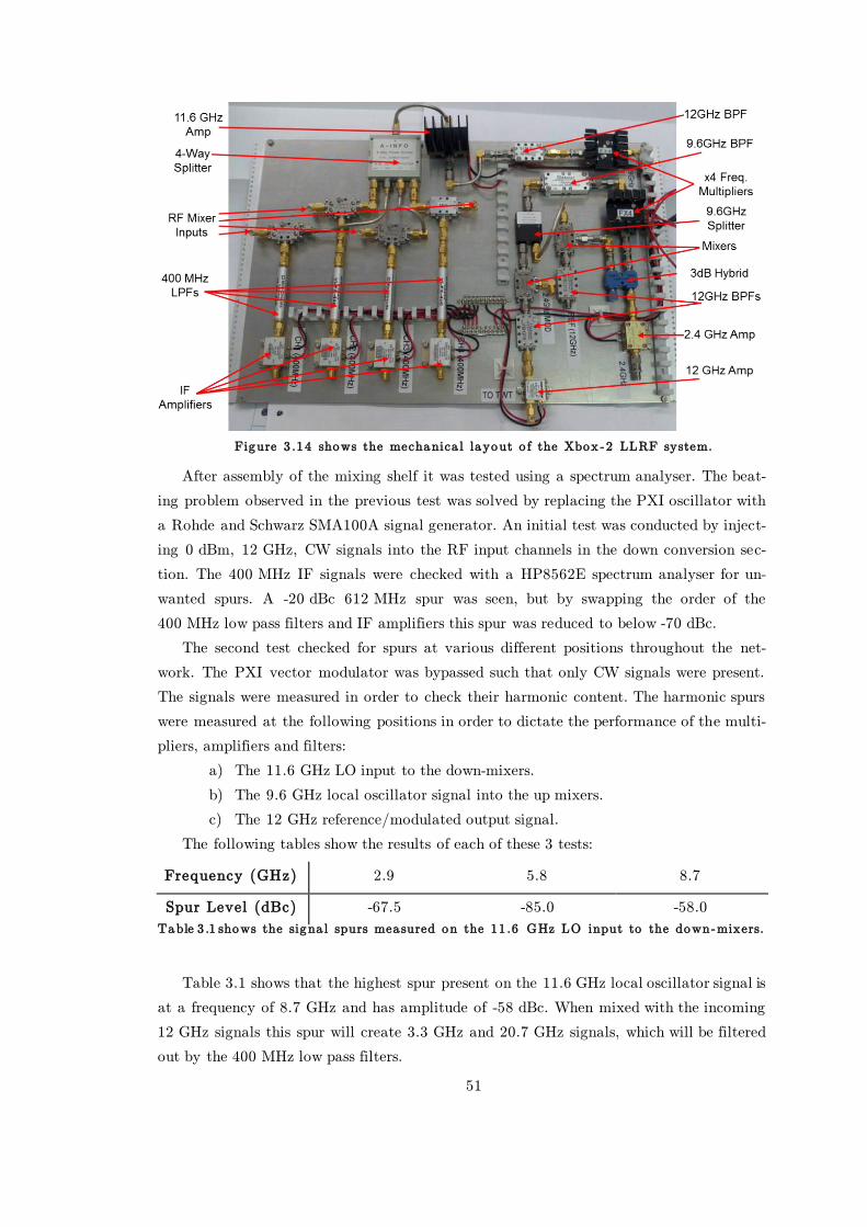
51
Figure 3 .14 shows the mechanica l layout o f the Xbox -2 LLRF system.
After assembly of the mixing shelf it was tested using a spectrum analyser. The beat-
ing problem observed in the previous test was solved by replacing the PXI oscillator with
a Rohde and Schwarz SMA100A signal generator. An initial test was conducted by inject-
ing 0 dBm, 12 GHz, CW signals into the RF input channels in the down conversion sec-
tion. The 400 MHz IF signals were checked with a HP8562E spectrum analyser for un-
wanted spurs. A -20 dBc 612 MHz spur was seen, but by swapping the order of the
400 MHz low pass filters and IF amplifiers this spur was reduced to below -70 dBc.
The second test checked for spurs at various different positions throughout the net-
work. The PXI vector modulator was bypassed such that only CW signals were present.
The signals were measured in order to check their harmonic content. The harmonic spurs
were measured at the following positions in order to dictate the performance of the multi-
pliers, amplifiers and filters:
a) The 11.6 GHz LO input to the down-mixers.
b) The 9.6 GHz local oscillator signal into the up mixers.
c) The 12 GHz reference/modulated output signal.
The following tables show the results of each of these 3 tests:
Frequency (GHz) 2.9 5.8 8.7
Spur Level (dBc) -67.5 -85.0 -58.0
Table 3 .1 shows the signa l spurs measured on the 11 .6 GHz LO input to the down-mixers.
Table 3.1 shows that the highest spur present on the 11.6 GHz local oscillator signal is
at a frequency of 8.7 GHz and has amplitude of -58 dBc. When mixed with the incoming
12 GHz signals this spur will create 3.3 GHz and 20.7 GHz signals, which will be filtered
out by the 400 MHz low pass filters.
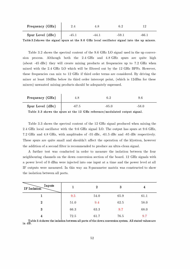
52
Frequency (GHz) 2.4 4.8 6.2 12
Spur Level (dBc) -45.1 -44.1 -59.1 -66.1
Table 3 .2 shows the signa l spurs a t the 9 .6 GHz lo ca l o scilla to r signa l into the up mixers .
Table 3.2 shows the spectral content of the 9.6 GHz LO signal used in the up conver-
sion process. Although both the 2.4 GHz and 4.8 GHz spurs are quite high
(about -45 dBc) they will create mixing products at frequencies up to 7.2 GHz when
mixed with the 2.4 GHz LO which will be filtered out by the 12 GHz BPFs. However,
these frequencies can mix to 12 GHz if third order terms are considered. By driving the
mixer at least 10dBm below its third order intercept point, (which is 12dBm for these
mixers) unwanted mixing products should be adequately supressed.
Frequency (GHz) 4.8 6.2 9.6
Spur Level (dBc) -67.5 -85.0 -58.0
Table 3 .3 shows the spurs a t the 12 GHz reference/modula ted output signa l.
Table 3.3 shows the spectral content of the 12 GHz signal produced when mixing the
2.4 GHz local oscillator with the 9.6 GHz signal LO. The output has spurs at 9.6 GHz,
7.2 GHz and 4.8 GHz, with amplitudes of -55 dBc, -61.5 dBc and -85 dBc respectively.
These spurs are quite small and shouldn’t affect the operation of the klystron, however
the addition of a second filter is recommended to produce an ultra-clean signal.
A further test was conducted in order to measure the isolation between the four
neighbouring channels on the down conversion section of the board. 12 GHz signals with
a power level of 0 dBm were injected into one input at a time and the power level at all
IF outputs were measured. In this way an S-parameter matrix was constructed to show
the isolation between all ports.
Inputs IF Isolation
1 2 3 4
1 9.5 54.0 65.9 61.1
2 51.0 9.4 62.5 58.0
3 66.3 63.3 9.7 68.0
4 72.5 61.7 76.5 9.7
Table 3 .4 shows the isolation between all ports of the down conversion system. All stated values a re in dB.
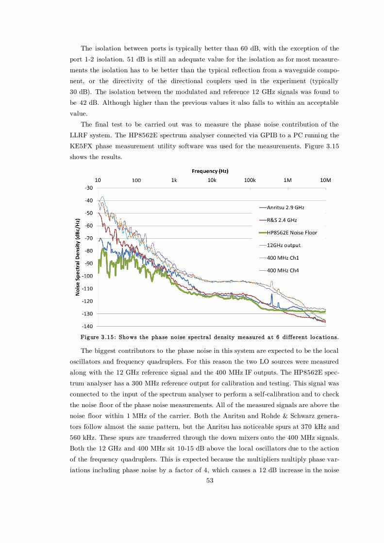
53
The isolation between ports is typically better than 60 dB, with the exception of the
port 1-2 isolation. 51 dB is still an adequate value for the isolation as for most measure-
ments the isolation has to be better than the typical reflection from a waveguide compo-
nent, or the directivity of the directional couplers used in the experiment (typically
30 dB). The isolation between the modulated and reference 12 GHz signals was found to
be 42 dB. Although higher than the previous values it also falls to within an acceptable
value.
The final test to be carried out was to measure the phase noise contribution of the
LLRF system. The HP8562E spectrum analyser connected via GPIB to a PC running the
KE5FX phase measurement utility software was used for the measurements. Figure 3.15
shows the results.
Figure 3 .15 : Shows the phase no ise spectra l density measured a t 6 diff erent lo ca tions.
The biggest contributors to the phase noise in this system are expected to be the local
oscillators and frequency quadruplers. For this reason the two LO sources were measured
along with the 12 GHz reference signal and the 400 MHz IF outputs. The HP8562E spec-
trum analyser has a 300 MHz reference output for calibration and testing. This signal was
connected to the input of the spectrum analyser to perform a self-calibration and to check
the noise floor of the phase noise measurements. All of the measured signals are above the
noise floor within 1 MHz of the carrier. Both the Anritsu and Rohde & Schwarz genera-
tors follow almost the same pattern, but the Anritsu has noticeable spurs at 370 kHz and
560 kHz. These spurs are transferred through the down mixers onto the 400 MHz signals.
Both the 12 GHz and 400 MHz sit 10-15 dB above the local oscillators due to the action
of the frequency quadruplers. This is expected because the multipliers multiply phase var-
iations including phase noise by a factor of 4, which causes a 12 dB increase in the noise
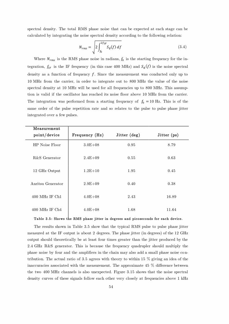
54
spectral density. The total RMS phase noise that can be expected at each stage can be
calculated by integrating the noise spectral density according to the following relation:
𝑁𝑟𝑚𝑠 = √2∫ 𝑆∅(𝑓) 𝑑𝑓2𝑓𝐼𝐹
𝑓0
(3.4)
Where 𝑁𝑟𝑚𝑠 is the RMS phase noise in radians, 𝑓0 is the starting frequency for the in-
tegration, 𝑓𝐼𝐹 is the IF frequency (in this case 400 MHz) and 𝑆∅(𝑓) is the noise spectral
density as a function of frequency 𝑓. Since the measurement was conducted only up to
10 MHz from the carrier, in order to integrate out to 800 MHz the value of the noise
spectral density at 10 MHz will be used for all frequencies up to 800 MHz. This assump-
tion is valid if the oscillator has reached its noise floor above 10 MHz from the carrier.
The integration was performed from a starting frequency of 𝑓0 = 10 Hz. This is of the
same order of the pulse repetition rate and so relates to the pulse to pulse phase jitter
integrated over a few pulses.
Measurement
point/device
Frequency (Hz)
Jitter (deg)
Jitter (ps)
HP Noise Floor 3.0E+08 0.95 8.79
R&S Generator 2.4E+09 0.55 0.63
12 GHz Output 1.2E+10 1.95 0.45
Anritsu Generator 2.9E+09 0.40 0.38
400 MHz IF Ch1 4.0E+08 2.43 16.89
400 MHz IF Ch4 4.0E+08 1.68 11.64
Table 3 .5 : Shows the RMS phase jitter in deg rees and pico seconds fo r ea ch device.
The results shown in Table 3.5 show that the typical RMS pulse to pulse phase jitter
measured at the IF output is about 2 degrees. The phase jitter (in degrees) of the 12 GHz
output should theoretically be at least four times greater than the jitter produced by the
2.4 GHz R&S generator. This is because the frequency quadrupler should multiply the
phase noise by four and the amplifiers in the chain may also add a small phase noise con-
tribution. The actual ratio of 3.5 agrees with theory to within 15 % giving an idea of the
inaccuracies associated with the measurement. The approximate 45 % difference between
the two 400 MHz channels is also unexpected. Figure 3.15 shows that the noise spectral
density curves of these signals follow each other very closely at frequencies above 1 kHz
55
from the carrier. However, at lower frequencies the measurements become more sporadic
contributing to the difference in measurement. This is the case for all of the acquired sig-
nals and could explain other discrepancies.
A direct phase noise measurement in the time domain can be completed for compari-
son with the noise spectral density measurements. The IQ demodulation using the PXI
crate can measure both the intra-pulse and pulse to pulse phase jitter directly.
Figure 3.16: Shows the phase and amplitude acquired by the LLRF and PXI system. Various methods a re used fo r the demodula tion and a re plo tted in different co lours.
Figure 3.16 shows the phase and amplitude of the down-mixed test and reference sig-
nals. The test signal has been demodulated via two different methods. The first uses
FPGA demodulation as described in Section 3.3.2, while the second uses the software
based demodulation described in Figure 3.12 (by mixing with the acquired reference sig-
nal). The reference signal has also itself been demodulated using the FPGA. By doing this
two different measurements can be made. The software based demodulation will measure
the phase noise between two adjacent channels: the one used to acquire the test signal
and the other used to acquire the reference signal. This same measurement can also be
performed by subtracting the phases of FPGA modulated test and reference signals. The
second measurement which uses only the FPGA test signal will measure the jitter of the
signal against the FPGA’s clock which is in turn locked to the master 10 MHz distribu-
tion. The second measurement should directly compare to that of the noise spectral densi-
ty method (because the spectrum analyser used, measured phase variations against the
master 10 MHz distribution.)
The RMS pulse to pulse phase jitter is measured by taking the average phase of the
signal (or phase the difference between two adjacent signals) in a 300 ns span for each
pulse. The values where sent to a circular buffer which stored 50 pulses (or one second ’s)
worth of data. The RMS of this array was then calculated. The results show that there
was approximately 0.24 degrees of pulse to phase jitter between adjacent channels. This
result was the same to within 1 % for both the software and FPGA demodulation meth-
ods. For real world measurements at the test stands (such as breakdown location meas-
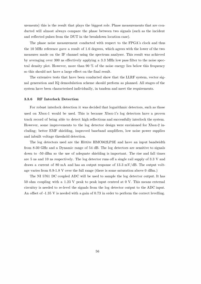
56
urements) this is the result that plays the biggest role. Phase measurements that are con-
ducted will almost always compare the phase between two signals (such as the incident
and reflected pulses from the DUT in the breakdown location case).
The phase noise measurement conducted with respect to the FPGA’s clock and thus
the 10 MHz reference gave a result of 1.6 degrees, which agrees with the lower of the two
measures made on the IF channel using the spectrum analyser. This result was achieved
by averaging over 300 ns effectively applying a 3.3 MHz low pass filter to the noise spec-
tral density plot. However, more than 90 % of the noise energy lies below this frequency
so this should not have a large effect on the final result.
The extensive tests that have been conducted show that the LLRF system, vector sig-
nal generation and IQ demodulation scheme should perform as planned. All stages of the
system have been characterised individually, in tandem and meet the requirements.
3.3.6 RF Interlock Detection
For robust interlock detection it was decided that logarithmic detectors, such as those
used on Xbox-1 would be used. This is because Xbox-1’s log detectors have a proven
track record of being able to detect high reflections and successfully interlock the system.
However, some improvements to the log detector design were envisioned for Xbox-2 in-
cluding; better EMF shielding, improved baseband amplifiers, low noise power supplies
and inbuilt voltage threshold detection.
The log detectors used are the Hittite HMC662LP3E and have an input bandwidth
from 8-30 GHz and a Dynamic range of 54 dB. The log detectors are sensitive to signals
down to -50 dBm so the use of adequate shielding is important. The rise and fall times
are 5 ns and 10 ns respectively. The log detector runs off a single rail supply of 3.3 V and
draws a current of 80 mA and has an output response of 13.3 mV/dB. The output volt-
age varies from 0.9-1.8 V over the full range (there is some saturation above 0 dBm.)
The NI 5761 DC coupled ADC will be used to sample the log detector output. It has
50 ohm coupling with a 1.23 V peak to peak input centred at 0 V. This means external
circuitry is needed to re-level the signals from the log detector output to the ADC input.
An offset of -1.35 V is needed with a gain of 0.73 in order to perform the correct levelling.
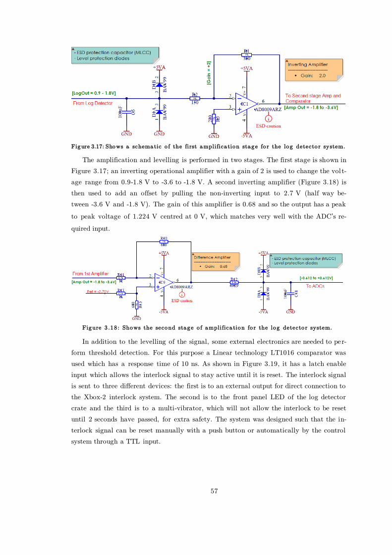
57
Figure 3.17: Shows a schematic o f the first amplifica tion stage fo r the log detecto r system.
The amplification and levelling is performed in two stages. The first stage is shown in
Figure 3.17; an inverting operational amplifier with a gain of 2 is used to change the volt-
age range from 0.9-1.8 V to -3.6 to -1.8 V. A second inverting amplifier (Figure 3.18) is
then used to add an offset by pulling the non-inverting input to 2.7 V (half way be-
tween -3.6 V and -1.8 V). The gain of this amplifier is 0.68 and so the output has a peak
to peak voltage of 1.224 V centred at 0 V, which matches very well with the ADC’s re-
quired input.
Figure 3 .18 : Shows the second stage o f amplifica tion fo r the log detecto r system.
In addition to the levelling of the signal, some external electronics are needed to per-
form threshold detection. For this purpose a Linear technology LT1016 comparator was
used which has a response time of 10 ns. As shown in Figure 3.19, it has a latch enable
input which allows the interlock signal to stay active until it is reset. The interlock signal
is sent to three different devices: the first is to an external output for direct connection to
the Xbox-2 interlock system. The second is to the front panel LED of the log detector
crate and the third is to a multi-vibrator, which will not allow the interlock to be reset
until 2 seconds have passed, for extra safety. The system was designed such that the in-
terlock signal can be reset manually with a push button or automatically by the control
system through a TTL input.
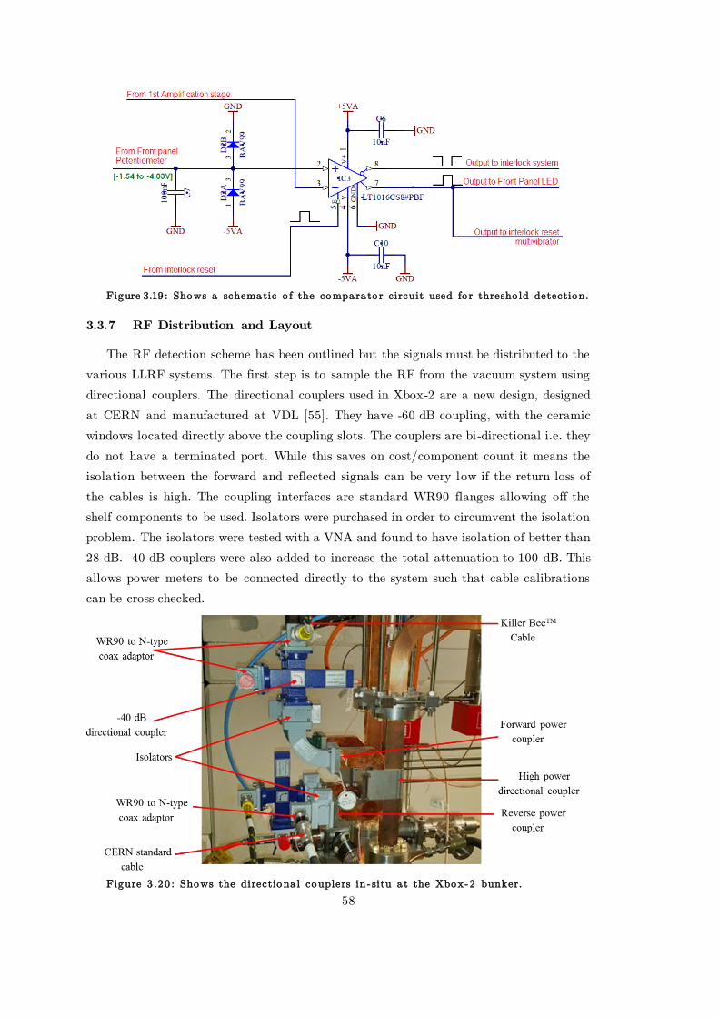
58
Figure 3.19 : Shows a schematic o f the compara to r circuit used fo r thresho ld detection.
3.3.7 RF Distribution and Layout
The RF detection scheme has been outlined but the signals must be distributed to the
various LLRF systems. The first step is to sample the RF from the vacuum system using
directional couplers. The directional couplers used in Xbox-2 are a new design, designed
at CERN and manufactured at VDL [55]. They have -60 dB coupling, with the ceramic
windows located directly above the coupling slots. The couplers are bi-directional i.e. they
do not have a terminated port. While this saves on cost/component count it means the
isolation between the forward and reflected signals can be very low if the return loss of
the cables is high. The coupling interfaces are standard WR90 flanges allowing off the
shelf components to be used. Isolators were purchased in order to circumvent the isolation
problem. The isolators were tested with a VNA and found to have isolation of better than
28 dB. -40 dB couplers were also added to increase the total attenuation to 100 dB. This
allows power meters to be connected directly to the system such that cable calibrations
can be cross checked.
Figure 3 .20 : Shows the directiona l couplers in - situ a t the Xbox -2 bunker.

59
In order for the signals to be launched into the coax cables WR90 to n-type adaptors
are used. Two types of coaxial cable are used; the standard CERN type and Megaphase
Killer BeeTM cables. The standard CERN cables are relatively cheap but suffer from the
calibration problems discussed in section 2.4.1. The Killer BeeTM cables however are pre-
fabricated such that their connectors are very stable when undergoing movement and/or
disconnection and reconnection. The cables themselves have been designed to have large
phase and insertion loss stabilities. Flexing the cables results in less than 1 degree phase
shift and 0.01 dB of insertion loss at 12 GHz and their temperature stability is 0.1 ppm at
25ºC. Although the cost of the cables is 50 times more than the standard cable, the re-
duced man hours needed for calibration should compensate for the extra cost. The cables
are used for the klystron output signal and those which are important for the device un-
der test (i.e. DUT incident, reflected and transmitted signals). The standard CERN ca-
bles are used for the reflected to klystron and reflected from load signals. The absolute
calibration is less important because the main purpose of these signals is machine protec-
tion and not precision measurements.
All of the RF cables terminate at the LLRF and control rack, positioned near the op-
erator’s desk (Figure 3.1). Inside the rack, the signals are passed through 12 GHz band
pass filters in order to filter out higher order harmonics generated in the TWT or klys-
tron. After, the signals are attenuated as not to saturate any of the RF detectors. The
signals are split into four such that each signal can be directed to different LLRF systems
as desired, as shown in Figure 3.21. Any unused outputs of the splitter are terminated
into 50 ohms.
Figure 3 .21 : shows a schematic o f the RF signa l distribution inside the LLRF rack.
One of the signal paths is sent to an ETL systems 23166-S5S5, 8:1, RF multiplexer.
This contains high quality RF relays for signal switching and can be controlled via Ether-
net or serial connection. It will be used in conjunction with a Rohde & Schwarz NRP-Z81
power sensor and NRP-2 base unit, also controlled over Ethernet connection. In this way
any signal in the test stand can be switched into the power head and its calibrated power
level found. The switch unit and power meter are on the same Ethernet network as the
PXI, such that the power levels for each channel can be read directly by the control sys-
tem (Figure 3.22).

60
Figure 3 .22 : Shows a schematic o f the power ca libra tion method tha t will be used.
All of the LLRF crates and the PXI crate were installed into a thermally insulated
rack, with a water cooled chiller unit installed. This was to keep the temperature levels
constant because much of the electronics used in the LLRF systems are temperature sen-
sitive. The chiller unit was connected to the 10ºC water circuit at the PS complex at
CERN.
Figure 3 .23 : Shows a front and back view o f the LLRF/contro ls ra ck a t Xbox -2 .
As shown in Figure 3.23 the RF cables enter the rack from the top, thus the RF dis-
tribution crate containing the 4-way RF splitters is placed at the top. Killer BeeTM cables
are used to distribute the signals to the different LLRF systems. Typically (and on Xbox-
1) semi-rigid cables are used, but we have found that the connectors can be very fragile
and have had to replace/repair many of them on Xbox-1. The RF multiplexer is placed
underneath the distribution crate, with the log detectors and down mixing crates under-
neath. There are two spaces left for passing cables from the front to the back of the rack.
The higher of the cable pass-throughs acts as a shelf containing the power sensor, RF

61
multiplexer and an Ethernet switch. This forms a network which interfaces the power me-
ter controller, RF multiplexer, modulator control system, the operator PC and the PXI
crate.
Below the PXI crate is the timing and trigger interface crate, which contains logic
levelling circuitry and EMF protection. This crate is discussed in further detail on section
3.6.3. The chiller unit sits at the base of the rack and blows cool air upwards at the front
and receives the warm air at the back to form a circulating current of air around the
rack.
3.4 New SLED-I Pulse Compressor
As described in section 3.2.2, a new pulse compressor has been designed for use at
Xbox-2. It is a type SLED-I pulse compressor, similar to that used in Xbox-1. The main
differences are that is uses a different RF mode in the storage cavities, has no on-line me-
chanical tuners and has a much more compact design.
3.4.1 SLED-I RF design
There are two main features that allow the new SLED to be compact. The first is the
design of the storage cavities which use an adiabatic taper at each end to ensure that un-
wanted modes are not produced. This allows a pure TE01 like mode to exist in the cavity,
which simplifies the task of the mode converters. The second are the mode converters
themselves; which are the very compact type used in the waveguide network at Xbox-1
(as described in Figure 2.6).
Figure 3.24: Shows the electric field pattern inside of the storage cavity o f the new SLED I [56 ].
Figure 3.24 shows how the adiabatic tapers at each end of the cavity reduce the radi-
us such that the TE02 and TE03 modes are below the cut-off frequency. Simulations
show that the couplings to the TE02 and TE03 modes at the operating frequency
are -60 dB and -69 dB respectively. The simulated intrinsic Q factor of the cavity is
1.78×10⁶ with a coupling factor of 5.85.
In order to reduce costs it was decided that ultra-precise machining would not be used
and the cavities would be fabricated at the CERN workshop. Due to the increased manu-
facturing error the cavity will need to be mechanically tuned to the correct frequency. To
reduce complexity a fixed piston tuning method was designed as shown in Figure 3.25.
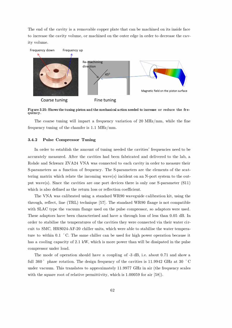
62
The end of the cavity is a removable copper plate that can be machined on its inside face
to increase the cavity volume, or machined on the outer edge in order to decrease the cav-
ity volume.
Figure 3.25: Shows the tuning piston and the mechanical a ction needed to increase o r reduce the fr e-quency.
The coarse tuning will impart a frequency variation of 20 MHz/mm, while the fine
frequency tuning of the chamfer is 1.1 MHz/mm.
3.4.2 Pulse Compressor Tuning
In order to establish the amount of tuning needed the cavities’ frequencies need to be
accurately measured. After the cavities had been fabricated and delivered to the lab, a
Rohde and Schwarz ZVA24 VNA was connected to each cavity in order to measure their
S-parameters as a function of frequency. The S-parameters are the elements of the scat-
tering matrix which relate the incoming wave(s) incident on an N-port system to the out-
put wave(s). Since the cavities are one port devices there is only one S-parameter (S11)
which is also defined as the return loss or reflection coefficient.
The VNA was calibrated using a standard WR90 waveguide calibration kit, using the
through, reflect, line (TRL) technique [57]. The standard WR90 flange is not compatible
with SLAC type the vacuum flange used on the pulse compressor, so adaptors were used.
These adaptors have been characterised and have a through loss of less than 0.05 dB. In
order to stabilise the temperatures of the cavities they were connected via their water ci r-
cuit to SMC, HRS024-AF-20 chiller units, which were able to stabilise the water tempera-
ture to within 0.1 ºC. The same chiller can be used for high power operation because it
has a cooling capacity of 2.1 kW, which is more power than will be dissipated in the pulse
compressor under load.
The mode of operation should have a coupling of -3 dB, i.e. about 0.71 and show a
full 360º phase rotation. The design frequency of the cavities is 11.9942 GHz at 30 ºC
under vacuum. This translates to approximately 11.9977 GHz in air (the frequency scales
with the square root of relative permittivity, which is 1.00059 for air [58]).
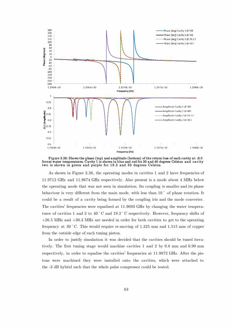
63
Figure 3.26: Shows the phase (top) and amplitude (bottom) of the return loss of each cavity a t di f-ferent water temperatures. Cavity 1 is shown in blue and red for 30 and 40 degrees Celsius and cavity two is shown in g reen and purple fo r 19 .2 and 30 deg rees Celsius.
As shown in Figure 3.26, the operating modes in cavities 1 and 2 have frequencies of
11.9712 GHz and 11.9674 GHz respectively. Also present is a mode about 4 MHz below
the operating mode that was not seen in simulation. Its coupling is smaller and its phase
behaviour is very different from the main mode, with less than 10º of phase rotation. It
could be a result of a cavity being formed by the coupling iris and the mode converter.
The cavities’ frequencies were equalised at 11.9693 GHz by changing the water tempera-
tures of cavities 1 and 2 to 40ºC and 19.2ºC respectively. However, frequency shifts of
+26.5 MHz and +30.3 MHz are needed in order for both cavities to get to the operating
frequency at 30ºC. This would require re-moving of 1.325 mm and 1.515 mm of copper
from the outside edge of each tuning piston.
In order to justify simulation it was decided that the cavities should be tuned itera-
tively. The first tuning stage would machine cavities 1 and 2 by 0.8 mm and 0.99 mm
respectively, in order to equalise the cavities’ frequencies at 11.9872 GHz. After the pis-
tons were machined they were installed onto the cavities, which were attached to
the -3 dB hybrid such that the whole pulse compressor could be tested.
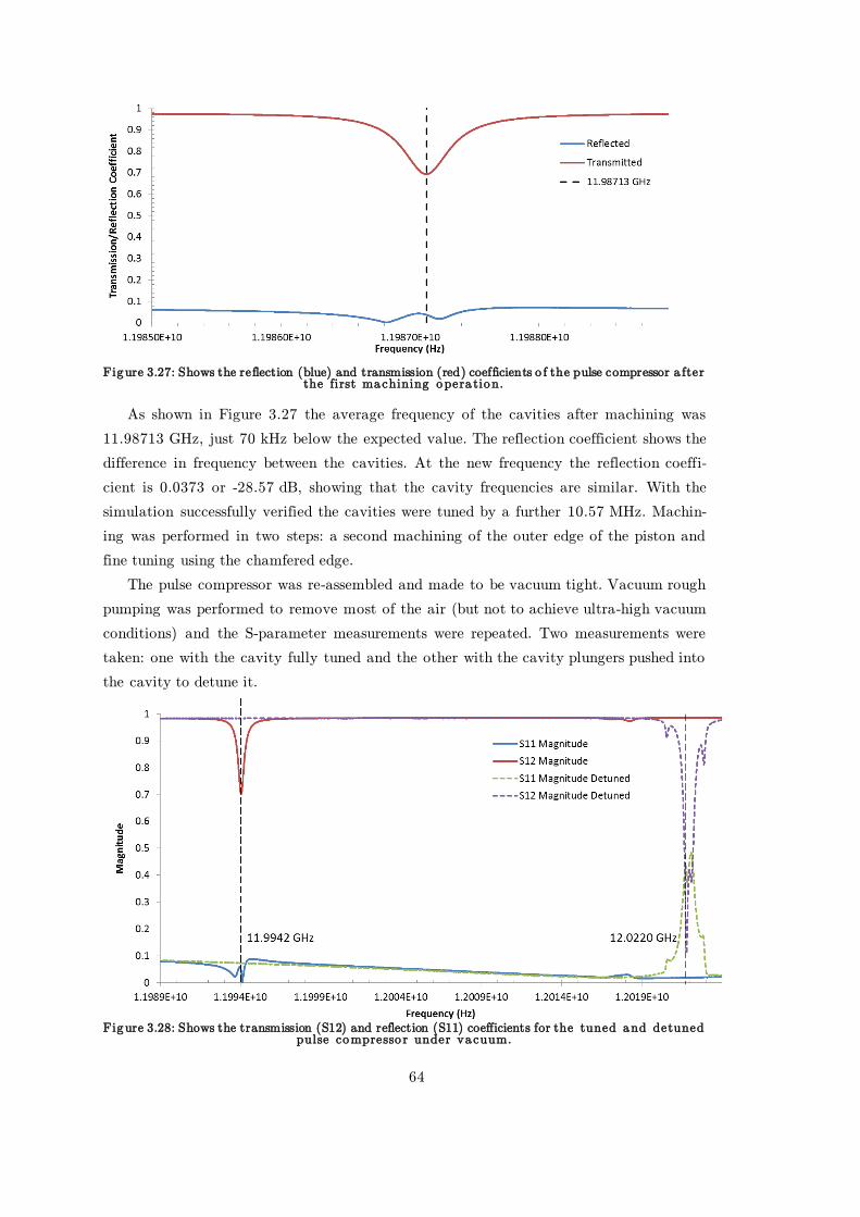
64
Figure 3.27: Shows the reflection (blue) and transmission (red) coefficients o f the pulse compressor a fter the first machining opera tion.
As shown in Figure 3.27 the average frequency of the cavities after machining was
11.98713 GHz, just 70 kHz below the expected value. The reflection coefficient shows the
difference in frequency between the cavities. At the new frequency the reflection coeffi-
cient is 0.0373 or -28.57 dB, showing that the cavity frequencies are similar. With the
simulation successfully verified the cavities were tuned by a further 10.57 MHz. Machin-
ing was performed in two steps: a second machining of the outer edge of the piston and
fine tuning using the chamfered edge.
The pulse compressor was re-assembled and made to be vacuum tight. Vacuum rough
pumping was performed to remove most of the air (but not to achieve ultra-high vacuum
conditions) and the S-parameter measurements were repeated. Two measurements were
taken: one with the cavity fully tuned and the other with the cavity plungers pushed into
the cavity to detune it.
Figure 3.28: Shows the transmission (S12) and reflection (S11) coefficients for the tuned and detuned
pulse compresso r under vacuum.
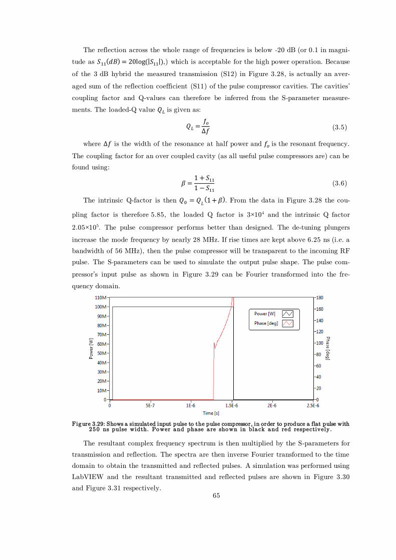
65
The reflection across the whole range of frequencies is below -20 dB (or 0.1 in magni-
tude as 𝑆11(𝑑𝐵) = 20log (|𝑆11|),) which is acceptable for the high power operation. Because
of the 3 dB hybrid the measured transmission (S12) in Figure 3.28, is actually an aver-
aged sum of the reflection coefficient (S11) of the pulse compressor cavities. The cavities’
coupling factor and Q-values can therefore be inferred from the S-parameter measure-
ments. The loaded-Q value 𝑄𝐿 is given as:
𝑄𝐿 =𝑓𝑜∆𝑓
(3.5)
where ∆𝑓 is the width of the resonance at half power and 𝑓𝑜 is the resonant frequency.
The coupling factor for an over coupled cavity (as all useful pulse compressors are) can be
found using:
𝛽 =1 + 𝑆11
1 − 𝑆11
(3.6)
The intrinsic Q-factor is then 𝑄0 = 𝑄𝐿(1+ 𝛽). From the data in Figure 3.28 the cou-
pling factor is therefore 5.85, the loaded Q factor is 3×10⁴ and the intrinsic Q factor
2.05×10⁵. The pulse compressor performs better than designed. The de-tuning plungers
increase the mode frequency by nearly 28 MHz. If rise times are kept above 6.25 ns (i.e. a
bandwidth of 56 MHz), then the pulse compressor will be transparent to the incoming RF
pulse. The S-parameters can be used to simulate the output pulse shape. The pulse com-
pressor’s input pulse as shown in Figure 3.29 can be Fourier transformed into the fre-
quency domain.
Figure 3.29: Shows a simulated input pulse to the pulse compressor, in order to produce a flat pulse with 250 ns pulse width. Power and phase a re shown in bla ck and red respectively .
The resultant complex frequency spectrum is then multiplied by the S-parameters for
transmission and reflection. The spectra are then inverse Fourier transformed to the time
domain to obtain the transmitted and reflected pulses. A simulation was performed using
LabVIEW and the resultant transmitted and reflected pulses are shown in Figure 3.30
and Figure 3.31 respectively.
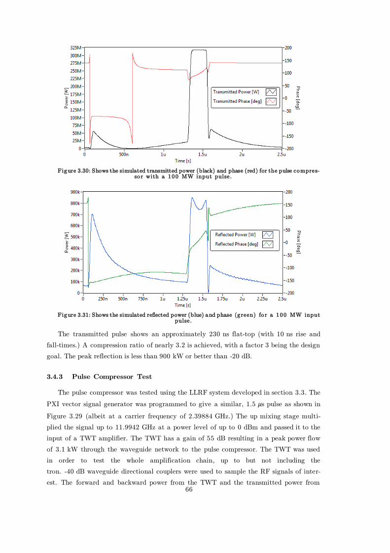
66
Figure 3.30: Shows the simulated transmitted power (black) and phase (red) for the pulse compres-so r with a 100 MW input pulse .
Figure 3.31: Shows the simulated reflected power (blue) and phase (g reen) fo r a 100 MW input pulse.
The transmitted pulse shows an approximately 230 ns flat-top (with 10 ns rise and
fall-times.) A compression ratio of nearly 3.2 is achieved, with a factor 3 being the design
goal. The peak reflection is less than 900 kW or better than -20 dB.
3.4.3 Pulse Compressor Test
The pulse compressor was tested using the LLRF system developed in section 3.3. The
PXI vector signal generator was programmed to give a similar, 1.5 𝜇s pulse as shown in
Figure 3.29 (albeit at a carrier frequency of 2.39884 GHz.) The up mixing stage multi-
plied the signal up to 11.9942 GHz at a power level of up to 0 dBm and passed it to the
input of a TWT amplifier. The TWT has a gain of 55 dB resulting in a peak power flow
of 3.1 kW through the waveguide network to the pulse compressor. The TWT was used
in order to test the whole amplification chain, up to but not including the
tron. -40 dB waveguide directional couplers were used to sample the RF signals of inter-
est. The forward and backward power from the TWT and the transmitted power from
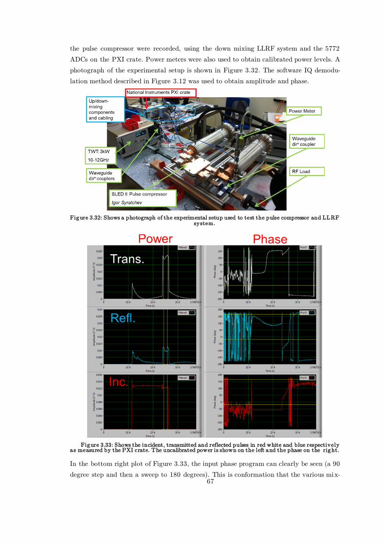
67
the pulse compressor were recorded, using the down mixing LLRF system and the 5772
ADCs on the PXI crate. Power meters were also used to obtain calibrated power levels. A
photograph of the experimental setup is shown in Figure 3.32. The software IQ demodu-
lation method described in Figure 3.12 was used to obtain amplitude and phase.
Figure 3.32: Shows a photograph of the experimental setup used to test the pulse compressor and LLRF system.
Figure 3.33: Shows the incident, transmitted and reflected pulses in red white and blue respectively a s measured by the PXI crate. The uncalibrated power is shown on the left and the phase on the right.
In the bottom right plot of Figure 3.33, the input phase program can clearly be seen (a 90
degree step and then a sweep to 180 degrees). This is conformation that the various mix-
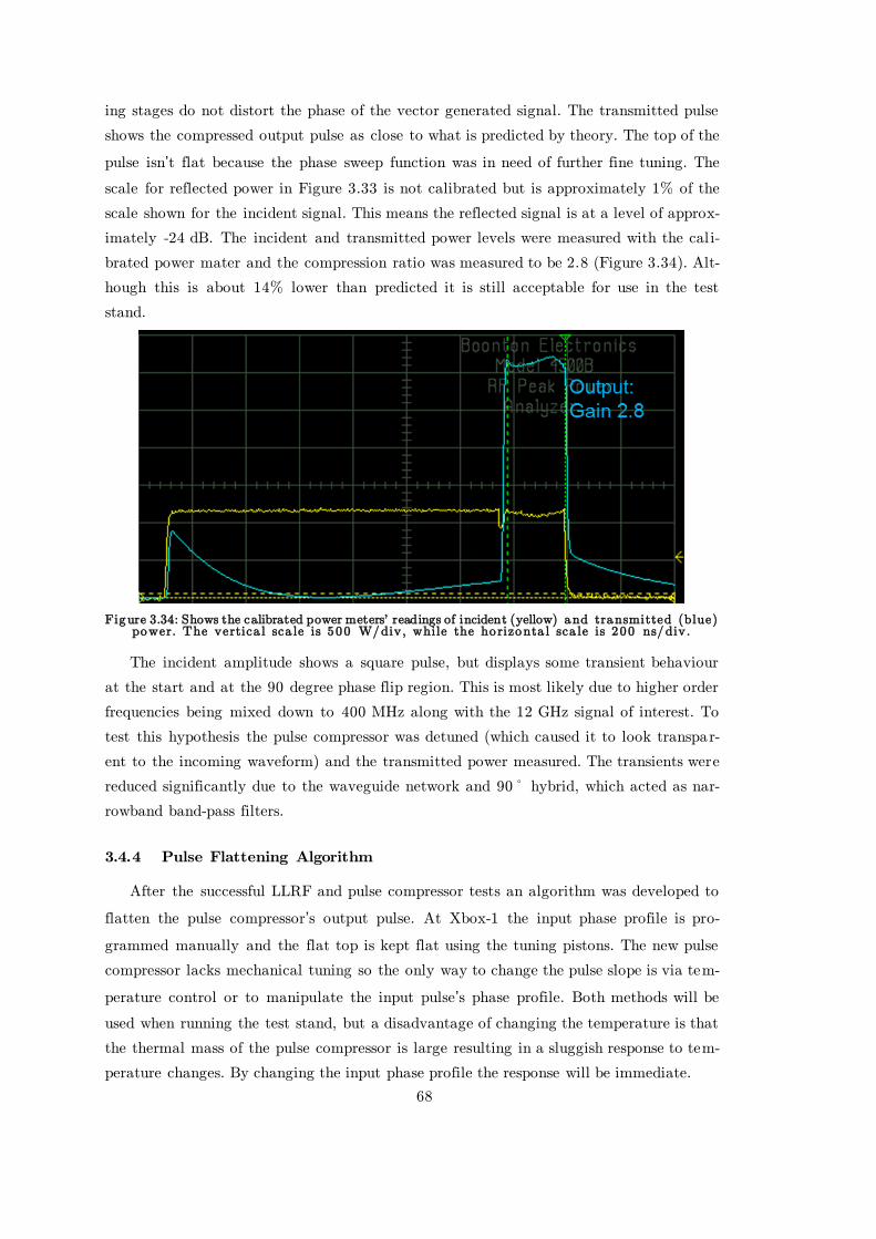
68
ing stages do not distort the phase of the vector generated signal. The transmitted pulse
shows the compressed output pulse as close to what is predicted by theory. The top of the
pulse isn’t flat because the phase sweep function was in need of further fine tuning. The
scale for reflected power in Figure 3.33 is not calibrated but is approximately 1% of the
scale shown for the incident signal. This means the reflected signal is at a level of approx-
imately -24 dB. The incident and transmitted power levels were measured with the cal i-
brated power mater and the compression ratio was measured to be 2.8 (Figure 3.34). Alt-
hough this is about 14% lower than predicted it is still acceptable for use in the test
stand.
Figure 3.34: Shows the calibrated power meters' readings of incident (yellow) and transmitted (blue) power. The vertica l sca le is 500 W/div, while the ho rizonta l sca le is 200 ns/div.
The incident amplitude shows a square pulse, but displays some transient behaviour
at the start and at the 90 degree phase flip region. This is most likely due to higher order
frequencies being mixed down to 400 MHz along with the 12 GHz signal of interest. To
test this hypothesis the pulse compressor was detuned (which caused it to look transpar-
ent to the incoming waveform) and the transmitted power measured. The transients were
reduced significantly due to the waveguide network and 90º hybrid, which acted as nar-
rowband band-pass filters.
3.4.4 Pulse Flattening Algorithm
After the successful LLRF and pulse compressor tests an algorithm was developed to
flatten the pulse compressor’s output pulse. At Xbox-1 the input phase profile is pro-
grammed manually and the flat top is kept flat using the tuning pistons. The new pulse
compressor lacks mechanical tuning so the only way to change the pulse slope is via tem-
perature control or to manipulate the input pulse’s phase profile. Both methods will be
used when running the test stand, but a disadvantage of changing the temperature is that
the thermal mass of the pulse compressor is large resulting in a sluggish response to tem-
perature changes. By changing the input phase profile the response will be immediate.
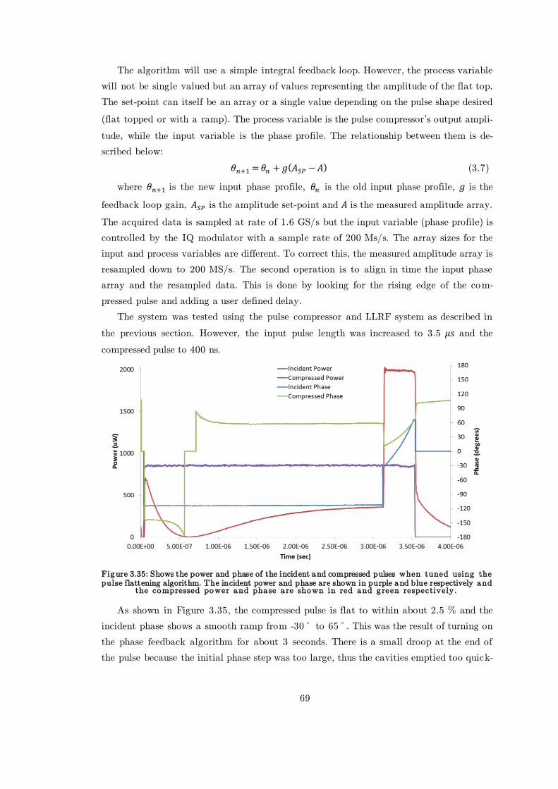
69
The algorithm will use a simple integral feedback loop. However, the process variable
will not be single valued but an array of values representing the amplitude of the flat top.
The set-point can itself be an array or a single value depending on the pulse shape desired
(flat topped or with a ramp). The process variable is the pulse compressor’s output ampli-
tude, while the input variable is the phase profile. The relationship between them is de-
scribed below:
𝜃𝑛+1 = 𝜃𝑛 + 𝑔(𝐴𝑆𝑃 − 𝐴) (3.7)
where 𝜃𝑛+1 is the new input phase profile, 𝜃𝑛 is the old input phase profile, 𝑔 is the
feedback loop gain, 𝐴𝑆𝑃 is the amplitude set-point and 𝐴 is the measured amplitude array.
The acquired data is sampled at rate of 1.6 GS/s but the input variable (phase profile) is
controlled by the IQ modulator with a sample rate of 200 Ms/s. The array sizes for the
input and process variables are different. To correct this, the measured amplitude array is
resampled down to 200 MS/s. The second operation is to align in time the input phase
array and the resampled data. This is done by looking for the rising edge of the com-
pressed pulse and adding a user defined delay.
The system was tested using the pulse compressor and LLRF system as described in
the previous section. However, the input pulse length was increased to 3.5 𝜇𝑠 and the
compressed pulse to 400 ns.
Figure 3.35: Shows the power and phase of the incident and compressed pulses when tuned using the pulse flattening algorithm. The incident power and phase are shown in purple and blue respectively and
the compressed power and phase a re shown in red and g reen respectively .
As shown in Figure 3.35, the compressed pulse is flat to within about 2.5 % and the
incident phase shows a smooth ramp from -30º to 65º. This was the result of turning on
the phase feedback algorithm for about 3 seconds. There is a small droop at the end of
the pulse because the initial phase step was too large, thus the cavities emptied too quick-
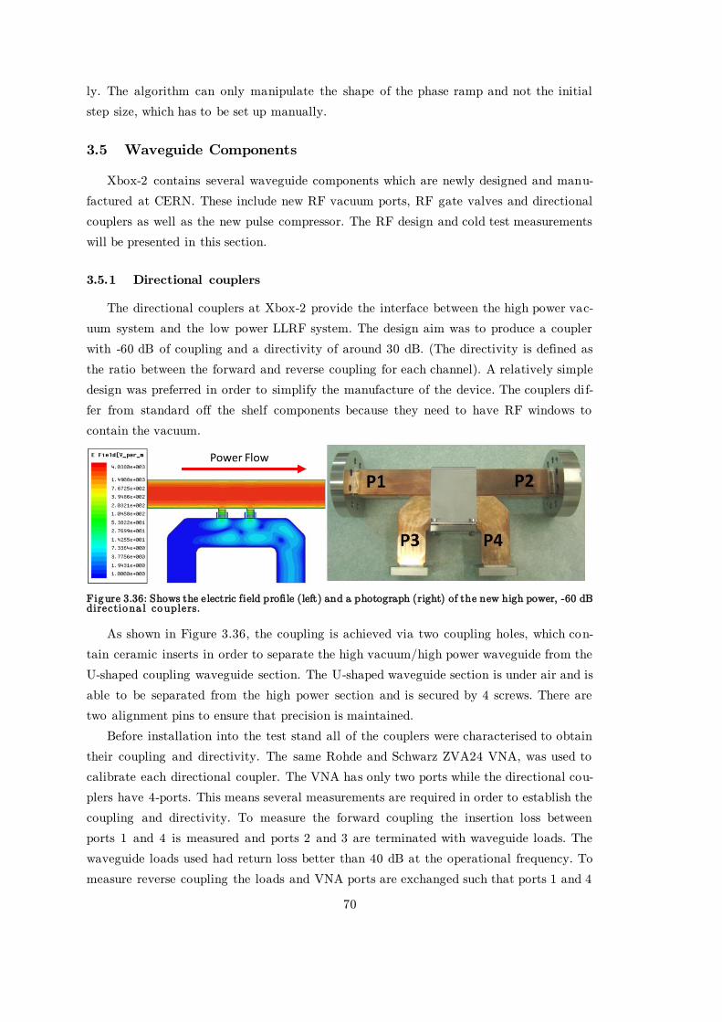
70
ly. The algorithm can only manipulate the shape of the phase ramp and not the initial
step size, which has to be set up manually.
3.5 Waveguide Components
Xbox-2 contains several waveguide components which are newly designed and manu-
factured at CERN. These include new RF vacuum ports, RF gate valves and directional
couplers as well as the new pulse compressor. The RF design and cold test measurements
will be presented in this section.
3.5.1 Directional couplers
The directional couplers at Xbox-2 provide the interface between the high power vac-
uum system and the low power LLRF system. The design aim was to produce a coupler
with -60 dB of coupling and a directivity of around 30 dB. (The directivity is defined as
the ratio between the forward and reverse coupling for each channel). A relatively simple
design was preferred in order to simplify the manufacture of the device. The couplers dif-
fer from standard off the shelf components because they need to have RF windows to
contain the vacuum.
Figure 3.36: Shows the electric field profile (left) and a photograph (right) of the new high power, -60 dB directiona l couplers.
As shown in Figure 3.36, the coupling is achieved via two coupling holes, which con-
tain ceramic inserts in order to separate the high vacuum/high power waveguide from the
U-shaped coupling waveguide section. The U-shaped waveguide section is under air and is
able to be separated from the high power section and is secured by 4 screws. There are
two alignment pins to ensure that precision is maintained.
Before installation into the test stand all of the couplers were characterised to obtain
their coupling and directivity. The same Rohde and Schwarz ZVA24 VNA, was used to
calibrate each directional coupler. The VNA has only two ports while the directional cou-
plers have 4-ports. This means several measurements are required in order to establish the
coupling and directivity. To measure the forward coupling the insertion loss between
ports 1 and 4 is measured and ports 2 and 3 are terminated with waveguide loads. The
waveguide loads used had return loss better than 40 dB at the operational frequency. To
measure reverse coupling the loads and VNA ports are exchanged such that ports 1 and 4
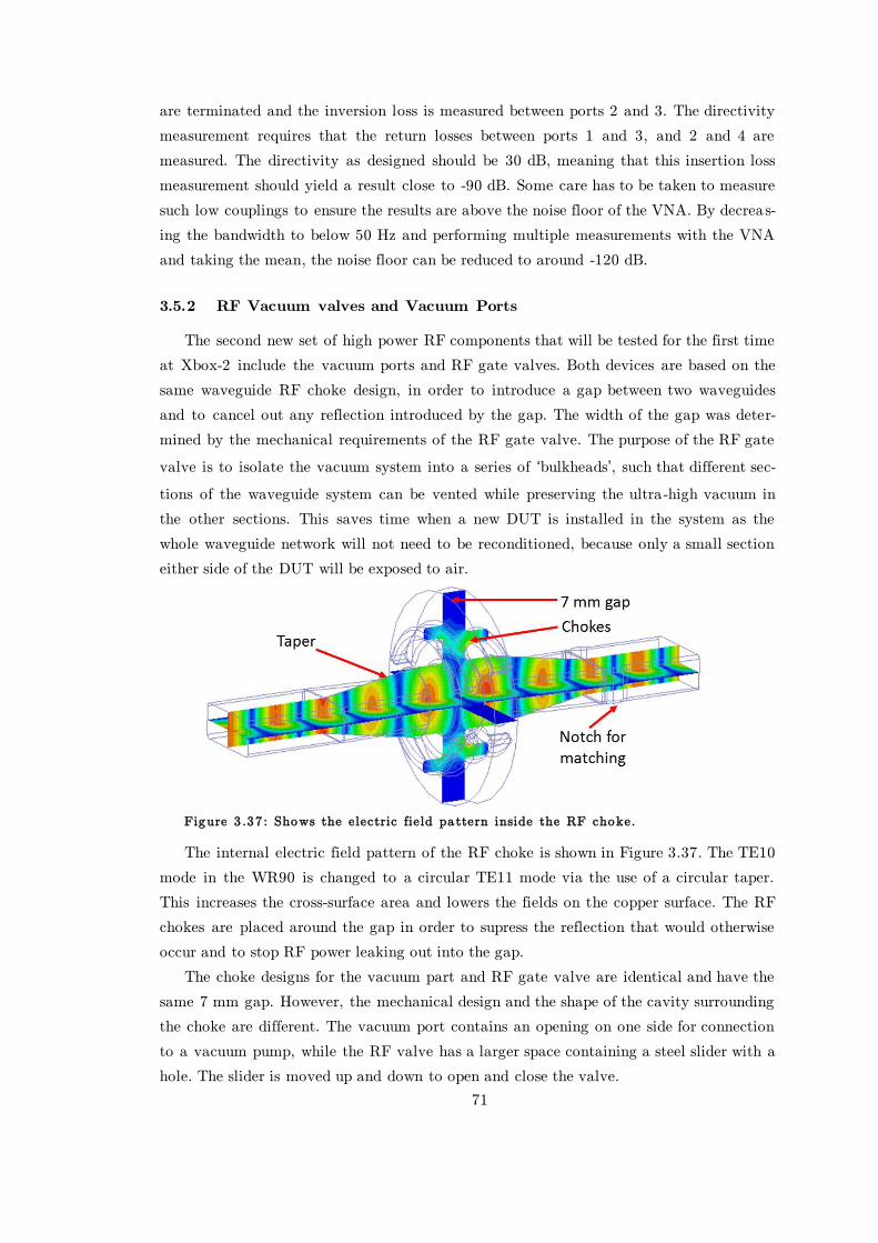
71
are terminated and the inversion loss is measured between ports 2 and 3. The directivity
measurement requires that the return losses between ports 1 and 3, and 2 and 4 are
measured. The directivity as designed should be 30 dB, meaning that this insertion loss
measurement should yield a result close to -90 dB. Some care has to be taken to measure
such low couplings to ensure the results are above the noise floor of the VNA. By decreas-
ing the bandwidth to below 50 Hz and performing multiple measurements with the VNA
and taking the mean, the noise floor can be reduced to around -120 dB.
3.5.2 RF Vacuum valves and Vacuum Ports
The second new set of high power RF components that will be tested for the first time
at Xbox-2 include the vacuum ports and RF gate valves. Both devices are based on the
same waveguide RF choke design, in order to introduce a gap between two waveguides
and to cancel out any reflection introduced by the gap. The width of the gap was deter-
mined by the mechanical requirements of the RF gate valve. The purpose of the RF gate
valve is to isolate the vacuum system into a series of ‘bulkheads’, such that different sec-
tions of the waveguide system can be vented while preserving the ultra -high vacuum in
the other sections. This saves time when a new DUT is installed in the system as the
whole waveguide network will not need to be reconditioned, because only a small section
either side of the DUT will be exposed to air.
Figure 3 .37 : Shows the electric fie ld pa ttern inside the RF choke.
The internal electric field pattern of the RF choke is shown in Figure 3.37. The TE10
mode in the WR90 is changed to a circular TE11 mode via the use of a circular taper.
This increases the cross-surface area and lowers the fields on the copper surface. The RF
chokes are placed around the gap in order to supress the reflection that would otherwise
occur and to stop RF power leaking out into the gap.
The choke designs for the vacuum part and RF gate valve are identical and have the
same 7 mm gap. However, the mechanical design and the shape of the cavity surrounding
the choke are different. The vacuum port contains an opening on one side for connection
to a vacuum pump, while the RF valve has a larger space containing a steel slider with a
hole. The slider is moved up and down to open and close the valve.
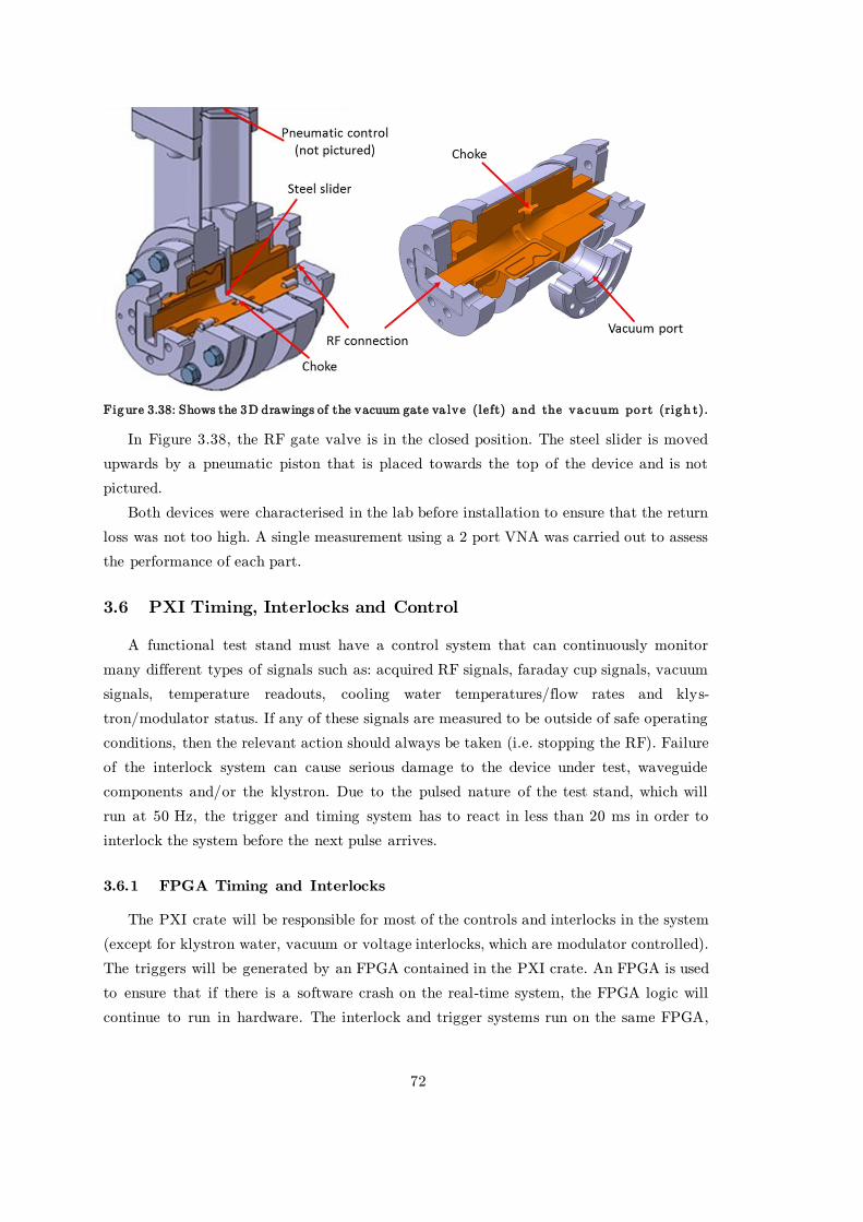
72
Figure 3.38: Shows the 3D drawings of the vacuum gate va lve (left) and the vacuum port (righ t).
In Figure 3.38, the RF gate valve is in the closed position. The steel slider is moved
upwards by a pneumatic piston that is placed towards the top of the device and is not
pictured.
Both devices were characterised in the lab before installation to ensure that the return
loss was not too high. A single measurement using a 2 port VNA was carried out to assess
the performance of each part.
3.6 PXI Timing, Interlocks and Control
A functional test stand must have a control system that can continuously monitor
many different types of signals such as: acquired RF signals, faraday cup signals, vacuum
signals, temperature readouts, cooling water temperatures/flow rates and klys-
tron/modulator status. If any of these signals are measured to be outside of safe operating
conditions, then the relevant action should always be taken (i.e. stopping the RF). Failure
of the interlock system can cause serious damage to the device under test, waveguide
components and/or the klystron. Due to the pulsed nature of the test stand, which will
run at 50 Hz, the trigger and timing system has to react in less than 20 ms in order to
interlock the system before the next pulse arrives.
3.6.1 FPGA Timing and Interlocks
The PXI crate will be responsible for most of the controls and interlocks in the system
(except for klystron water, vacuum or voltage interlocks, which are modulator controlled).
The triggers will be generated by an FPGA contained in the PXI crate. An FPGA is used
to ensure that if there is a software crash on the real-time system, the FPGA logic will
continue to run in hardware. The interlock and trigger systems run on the same FPGA,
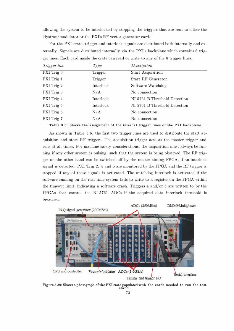
73
allowing the system to be interlocked by stopping the triggers that are sent to either the
klystron/modulator or the PXI’s RF vector generator card.
For the PXI crate, trigger and interlock signals are distributed both internally and ex-
ternally. Signals are distributed internally via the PXI’s backplane which contains 8 trig-
ger lines. Each card inside the crate can read or write to any of the 8 trigger lines.
Trigger line Type Description
PXI Trig 0 Trigger Start Acquisition
PXI Trig 1 Trigger Start RF Generator
PXI Trig 2 Interlock Software Watchdog
PXI Trig 3 N/A No connection
PXI Trig 4 Interlock NI 5761 B Threshold Detection
PXI Trig 5 Interlock NI 5761 B Threshold Detection
PXI Trig 6 N/A No connection
PXI Trig 7 N/A No connection
Table 3 .6 : Shows the a ssignment o f the interna l trigger lines o f the PXI backplane.
As shown in Table 3.6, the first two trigger lines are used to distribute the start ac-
quisition and start RF triggers. The acquisition trigger acts as the master trigger and
runs at all times. For machine safety considerations, the acquisition must always be run-
ning if any other system is pulsing, such that the system is being observed. The RF trig-
ger on the other hand can be switched off by the master timing FPGA, if an interlock
signal is detected. PXI Trig 2, 4 and 5 are monitored by the FPGA and the RF trigger is
stopped if any of these signals is activated. The watchdog interlock is activated if the
software running on the real time system fails to write to a register on the FPGA within
the timeout limit, indicating a software crash. Triggers 4 and/or 5 are written to by the
FPGAs that control the NI 5761 ADCs if the acquired data interlock threshold is
breached.
Figure 3.39: Shows a photograph of the PXI crate populated with the ca rds needed to run the test stand.

74
External trigger distribution is handled by an extension card attached to the timing
and trigger I/O FPGA as shown in Figure 3.39. The FPGA’s extender card is the
NI 6583, which contains buffers to interface the FPGA circuitry to LVTTL levels. I t has
35 I/O channels which can be individually configured to be an input or an output. An
external crate containing EMF protection and levelling to TTL voltages that can drive
long 50 ohm lines is used and is described in section 3.6.3.
External outputs include, triggers for the klystron, TWT and other equipment such as
power meters and oscilloscopes. The interlock status is also output such that external
equipment can be interlocked (or resumed) by the system (e.g. the log detector crate in-
terlock reset signal). There is one external trigger input for synchronising the timing to
the electricity main’s network zero crossing. This will reduce noise induced by power sup-
plies. The remainder of the inputs are used for interlocking. Signals used include: the vac-
uum controller threshold relays, the modulator status relays and the log detector thresh-
old interlock signals. Each input interlock signal can be set to be active high or active low
in the software. There are two levels of criticality for the interlocks that can also be pre-
configured in software. The so called ‘master’ interlocks will stop the LLRF trigger and
can be automatically reset by the software. This type of interlock will be triggered for
small vacuum spikes and high reflected power events which are expected during break-
down events. On the other hand, the ‘critical’ interlocks will stop the modulator trigger
and cannot be reset automatically. Very large vacuum spikes and modulator interlocks
will fall under this category.
3.6.2 Software Control and Interlocks
There are many other signals that are monitored that do not have a binary (or
on/off) representation. These are either analogue voltage signals, such as a voltage output
of a vacuum controller or a numerical value read over a serial connection. Devices con-
nected to the system via serial connection include: vacuum ion pump/gauge controllers,
temperature sensor controllers, chiller units, RF multiplexers and the modulator control
system. The voltage signals are read by the multiplexer and DMM unit in the PXI crate,
while the serial connections are read by RS485 or RS232 ports on the PXI crate. These
signals are not FPGA controlled but go through the main software architecture. Various
software threshold detectors check the parameters and if any are outside of nominal
bounds a software interlock signal is sent to the FPGA to stop the RF trigger.
3.6.3 Timing and Interlocks Interface PCB
The timing FPGA on the PXI crate required external voltage levelling and EMF pro-
tection. The interface to the PXI crate uses LVTTL logic, which has a voltage of 3.3 V
and a maximum output current of +/- 18 mA. This voltage and current is not large
enough to drive a 50 ohm terminated line to the 2 V required to trigger most TTL level
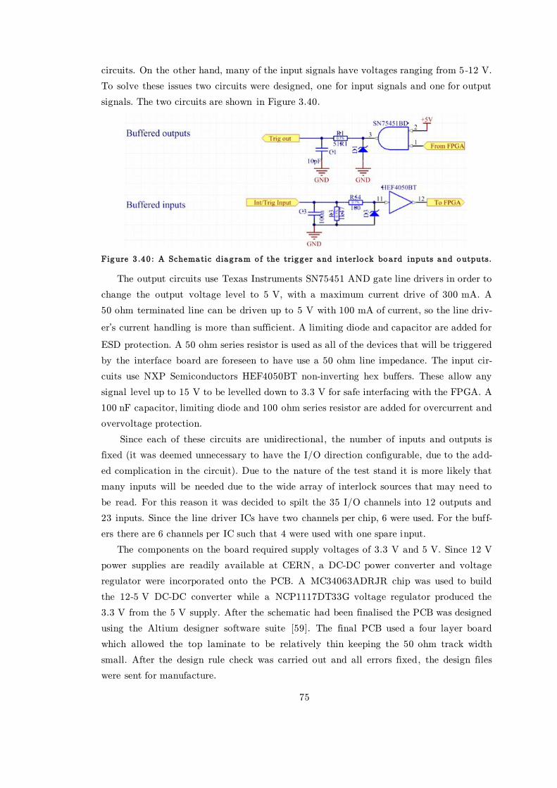
75
circuits. On the other hand, many of the input signals have voltages ranging from 5-12 V.
To solve these issues two circuits were designed, one for input signals and one for output
signals. The two circuits are shown in Figure 3.40.
Figure 3 .40 : A Schematic diag ram o f the trigger and interlo ck boa rd inputs and outputs.
The output circuits use Texas Instruments SN75451 AND gate line drivers in order to
change the output voltage level to 5 V, with a maximum current drive of 300 mA. A
50 ohm terminated line can be driven up to 5 V with 100 mA of current, so the line driv-
er’s current handling is more than sufficient. A limiting diode and capacitor are added for
ESD protection. A 50 ohm series resistor is used as all of the devices that will be triggered
by the interface board are foreseen to have use a 50 ohm line impedance. The input cir-
cuits use NXP Semiconductors HEF4050BT non-inverting hex buffers. These allow any
signal level up to 15 V to be levelled down to 3.3 V for safe interfacing with the FPGA. A
100 nF capacitor, limiting diode and 100 ohm series resistor are added for overcurrent and
overvoltage protection.
Since each of these circuits are unidirectional, the number of inputs and outputs is
fixed (it was deemed unnecessary to have the I/O direction configurable, due to the add-
ed complication in the circuit). Due to the nature of the test stand it is more likely that
many inputs will be needed due to the wide array of interlock sources that may need to
be read. For this reason it was decided to spilt the 35 I/O channels into 12 outputs and
23 inputs. Since the line driver ICs have two channels per chip, 6 were used. For the buff-
ers there are 6 channels per IC such that 4 were used with one spare input.
The components on the board required supply voltages of 3.3 V and 5 V. Since 12 V
power supplies are readily available at CERN, a DC-DC power converter and voltage
regulator were incorporated onto the PCB. A MC34063ADRJR chip was used to build
the 12-5 V DC-DC converter while a NCP1117DT33G voltage regulator produced the
3.3 V from the 5 V supply. After the schematic had been finalised the PCB was designed
using the Altium designer software suite [59]. The final PCB used a four layer board
which allowed the top laminate to be relatively thin keeping the 50 ohm track width
small. After the design rule check was carried out and all errors fixed, the design files
were sent for manufacture.

76
Upon delivery of the PCB, stencil and components, the board was fully assembled and
tested. After some minor modifications had been made the board performed to expecta-
tions. The board was then placed into a crate with 35 BNC feedthroughs and a 12 V
power supply (Figure 3.41).
Figure 3.41: Shows a pho tog raph o f the completed timing and interlo ck interfa ce cra te.
3.6.4 Vacuum and Temperature Controls Rack
All of the waveguide network’s vacuum and temperature controllers are placed into a
separate rack. These systems do not require temperature stabilization and so are not re-
quired to go inside the temperature cooled rack. Other equipment that doesn’t require
high thermal stability such as the TWT and dipole magnet power supply are placed in
the rack.
The rack’s layout is shown in Figure 3.42. Not labelled, but also contained in the rack
are breakout boxes attached to the PXI ’s DMM and interlock cards. The DMM connec-
tion allows analogue voltage signals, such as the klystron’s ion pump currents to be read
by the control system. The signals pass via a multi-conductor cable in a cable tray pass-
ing over the klystron access door. This same cable tray also contains the TWT output
cable which carries the kilowatt-level RF signal to the klystron.
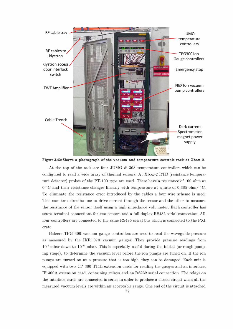
77
Figure 3.42: Shows a pho tog raph o f the vacuum and tempera ture contro ls ra ck a t Xbox -2 .
At the top of the rack are four JUMO di 308 temperature controllers which can be
configured to read a wide array of thermal sensors. At Xbox-2 RTD (resistance tempera-
ture detector) probes of the PT-100 type are used. These have a resistance of 100 ohm at
0ºC and their resistance changes linearly with temperature at a rate of 0.385 ohm/ºC.
To eliminate the resistance error introduced by the cables a four wire scheme is used.
This uses two circuits: one to drive current through the sensor and the other to measure
the resistance of the sensor itself using a high impedance volt meter. Each controller has
screw terminal connections for two sensors and a full duplex RS485 serial connection. All
four controllers are connected to the same RS485 serial bus which is connected to the PXI
crate.
Balzers TPG 300 vacuum gauge controllers are used to read the waveguide pressure
as measured by the IKR 070 vacuum gauges. They provide pressure readings from
10-3 mbar down to 10-11 mbar. This is especially useful during the initial (or rough pump-
ing stage), to determine the vacuum level before the ion pumps are tuned on. If the ion
pumps are turned on at a pressure that is too high, they can be damaged. Each unit is
equipped with two CP 300 T11L extension cards for reading the gauges and an interface,
IF 300A extension card, containing relays and an RS232 serial connection. The relays on
the interface cards are connected in series in order to produce a closed circuit when all the
measured vacuum levels are within an acceptable range. One end of the circuit is attached
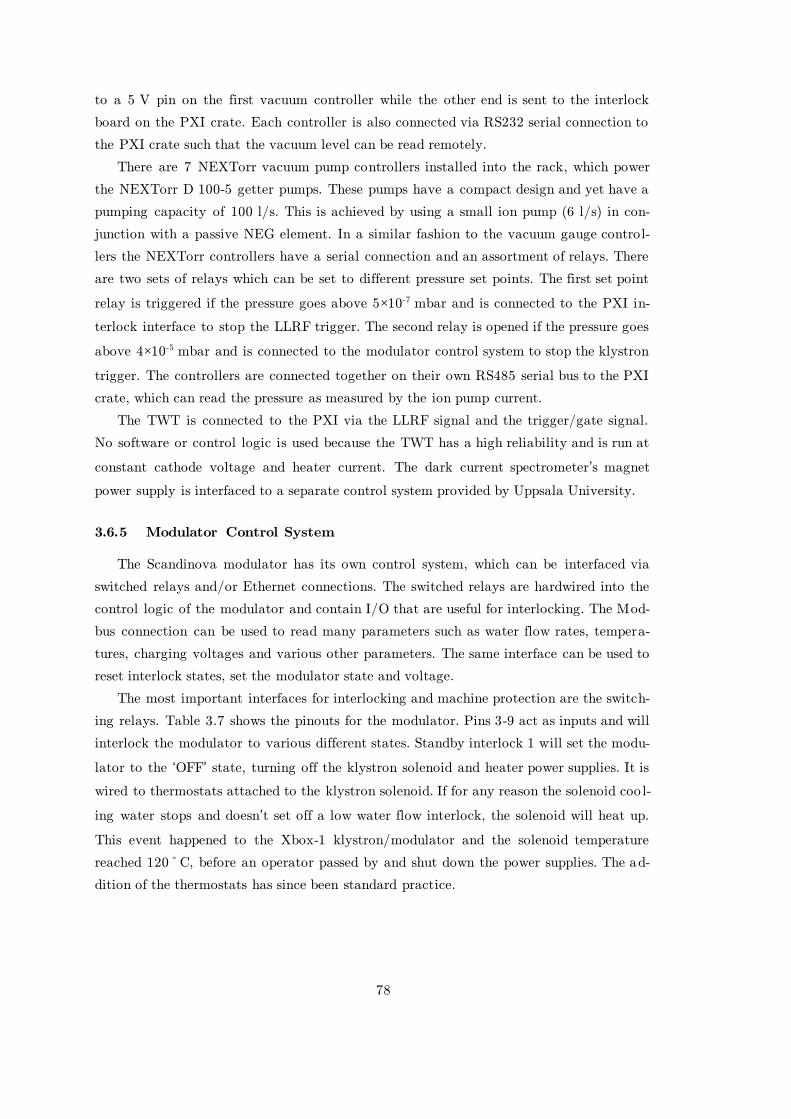
78
to a 5 V pin on the first vacuum controller while the other end is sent to the interlock
board on the PXI crate. Each controller is also connected via RS232 serial connection to
the PXI crate such that the vacuum level can be read remotely.
There are 7 NEXTorr vacuum pump controllers installed into the rack, which power
the NEXTorr D 100-5 getter pumps. These pumps have a compact design and yet have a
pumping capacity of 100 l/s. This is achieved by using a small ion pump (6 l/s) in con-
junction with a passive NEG element. In a similar fashion to the vacuum gauge control-
lers the NEXTorr controllers have a serial connection and an assortment of relays. There
are two sets of relays which can be set to different pressure set points. The first set point
relay is triggered if the pressure goes above 5×10⁻⁷ mbar and is connected to the PXI in-
terlock interface to stop the LLRF trigger. The second relay is opened if the pressure goes
above 4×10⁻⁵ mbar and is connected to the modulator control system to stop the klystron
trigger. The controllers are connected together on their own RS485 serial bus to the PXI
crate, which can read the pressure as measured by the ion pump current.
The TWT is connected to the PXI via the LLRF signal and the trigger/gate signal.
No software or control logic is used because the TWT has a high reliability and is run at
constant cathode voltage and heater current. The dark current spectrometer’s magnet
power supply is interfaced to a separate control system provided by Uppsala University.
3.6.5 Modulator Control System
The Scandinova modulator has its own control system, which can be interfaced via
switched relays and/or Ethernet connections. The switched relays are hardwired into the
control logic of the modulator and contain I/O that are useful for interlocking. The Mod-
bus connection can be used to read many parameters such as water flow rates, tempera-
tures, charging voltages and various other parameters. The same interface can be used to
reset interlock states, set the modulator state and voltage.
The most important interfaces for interlocking and machine protection are the switch-
ing relays. Table 3.7 shows the pinouts for the modulator. Pins 3-9 act as inputs and will
interlock the modulator to various different states. Standby interlock 1 will set the modu-
lator to the ‘OFF’ state, turning off the klystron solenoid and heater power supplies. It is
wired to thermostats attached to the klystron solenoid. If for any reason the solenoid coo l-
ing water stops and doesn’t set off a low water flow interlock, the solenoid will heat up.
This event happened to the Xbox-1 klystron/modulator and the solenoid temperature
reached 120ºC, before an operator passed by and shut down the power supplies. The ad-
dition of the thermostats has since been standard practice.

79
Table 3 .7 : Shows the switched relay opera tions o f the Scandinova modula to r a t Xbox -2 .
‘Hv interlock 1’ (or high voltage interlock 1) is wired to the klystron access doors and
will set the modulator state to ‘STANDBY’ if they are opened. In this state the solenoid
and heater is on but the high voltage power supplies are not charged. If someone tries to
access the rear of the modulator they must go through the interlocked doors. Similarly,
‘Hv interlock 2’ is activated when the bunker access key is removed from the modulator.
The bunker access door requires the key to open, which is locked in place (in the bunker
door’s lock mechanism) while the bunker remains open. It can only be removed by locking
the bunker. In order to pulse the modulator the key must be returned to the modulator.
Trigger interlock 1 is connected to the NEXTorr vacuum controllers and inhibits the
modulator trigger. The vacuum controllers output a signal if the vacuum level goes over
4×10⁻⁵ mbar in the waveguide network, thus stopping the klystron and RF. All other in-
puts are currently unused.
The ‘Sum interlock’ and ‘Hv’ outputs are both connected to the FPGA timing board.
The ‘Sum interlock’ output is high if the modulator has any active interlocks, while the

80
‘Hv’ output is active if the modulator’s charging power supplies are not charged. Both of
these signals need to be low if the PXI crate is to send a trigger to the klystron.
All of the relays’ I/O are active at all times even if the modulator is set to run on ‘lo-
cal’ mode. However, the modulator can be controlled remotely via an Ethernet/Modbus
connection. This mode of operation is not essential when running the test stand, for ex-
ample Xbox-1 runs without any communication between the PXI crate and the modula-
tor. Nevertheless, having the option to interface with the modulator is useful in certain
situations. Software was written such that the PXI crate could control the modulator
state and read various parameters such as: heater current and voltage, charging voltage,
pulse width etc.
3.7 Test stand Commissioning
The commissioning of the test stand is a full system test up to high power, to check
that all aspects of the system are working and that the system can run safely while un-
manned. The software and GUI is be tested, all interlock systems checked, RF lines cali-
brated and the waveguide components conditioned up to their nominal power levels.
3.7.1 General User Interface
The Xbox-2 software has to control all of the various systems described previously.
The software runs fully independently on the real time operating system on the PXI. The
PXI interfaces to the operator PC which displays the incoming signals and is used to
change software parameters. As shown in Figure 3.43, the GUI has a main operation win-
dow which shows a graph of all of the incoming RF signals, modulator status and general
interlock status. The software is modular and has different windows for each system
which can be opened from the main window.
Upon starting the software for the first time, the PC checks that the PXI ’s software is
running and ready to be configured. This information is displayed in the top left of the
window. The ‘Connect’ button is then pressed by the operator which runs all of the ini-
tialisation routines for each of the software blocks on the real time system. As each sys-
tem is successfully initialised the status is given in the system log display at the bottom
of the window. If any errors occur, an error code and a process name are shown to help
with debugging. After the successful initialisation, the ‘Load Config’ button is used to
load an xml file containing a full configuration profile for all user defined variables in the
system. This xml file is created using a separate VI (LabVIEW virtual instrument) by the
operator, usually during the previous successful run of the software. Once the variables
have been loaded from the configuration file, the ‘Start’ button is pressed which starts all
of the control loops and the system is ready to use.
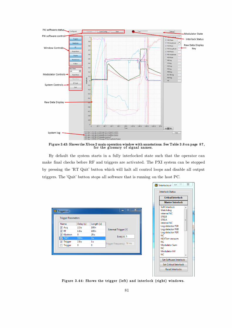
81
Figure 3.43: Shows the Xbox-2 main operation window with annotations. See Table 3 .8 on page 87 , fo r the g lo ssa ry o f signa l names.
By default the system starts in a fully interlocked state such that the operator can
make final checks before RF and triggers are activated. The PXI system can be stopped
by pressing the ‘RT Quit’ button which will halt all control loops and disable all output
triggers. The ‘Quit’ button stops all software that is running on the host PC.
Figure 3 .44 : Shows the trigger (left) and interlo ck (right) windows.
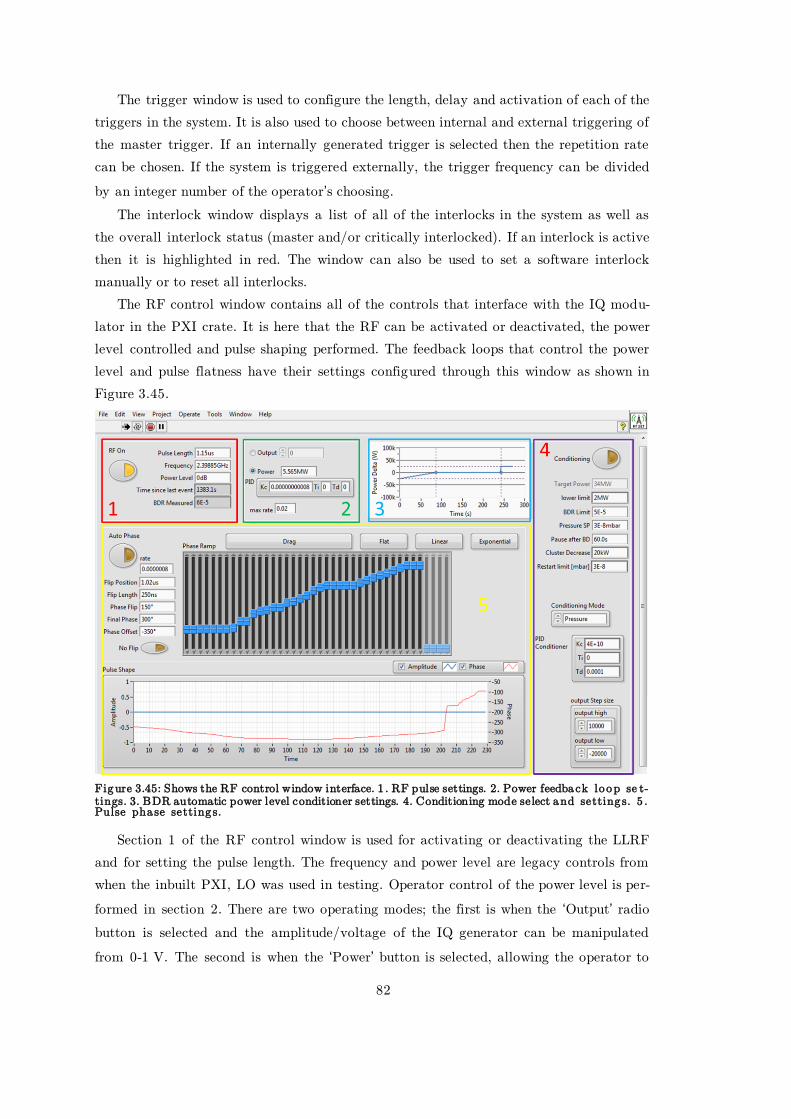
82
The trigger window is used to configure the length, delay and activation of each of the
triggers in the system. It is also used to choose between internal and external triggering of
the master trigger. If an internally generated trigger is selected then the repetition rate
can be chosen. If the system is triggered externally, the trigger frequency can be divided
by an integer number of the operator’s choosing.
The interlock window displays a list of all of the interlocks in the system as well as
the overall interlock status (master and/or critically interlocked). If an interlock is active
then it is highlighted in red. The window can also be used to set a software interlock
manually or to reset all interlocks.
The RF control window contains all of the controls that interface with the IQ modu-
lator in the PXI crate. It is here that the RF can be activated or deactivated, the power
level controlled and pulse shaping performed. The feedback loops that control the power
level and pulse flatness have their settings configured through this window as shown in
Figure 3.45.
Figure 3.45: Shows the RF control window interface. 1 . RF pulse settings. 2. Power feedback loop se t-tings. 3. BDR automatic power level conditioner settings. 4. Conditioning mode select and setting s. 5 . Pulse pha se setting s.
Section 1 of the RF control window is used for activating or deactivating the LLRF
and for setting the pulse length. The frequency and power level are legacy controls from
when the inbuilt PXI, LO was used in testing. Operator control of the power level is per-
formed in section 2. There are two operating modes; the first is when the ‘Output’ radio
button is selected and the amplitude/voltage of the IQ generator can be manipulated
from 0-1 V. The second is when the ‘Power’ button is selected, allowing the operator to
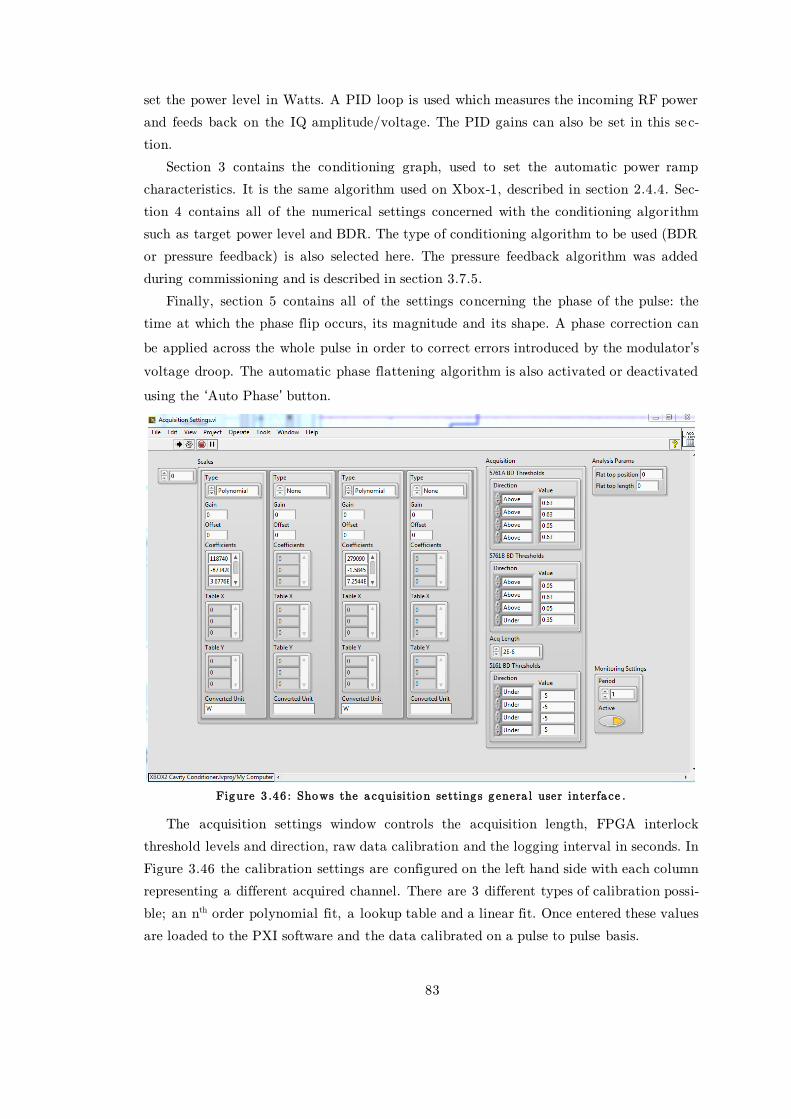
83
set the power level in Watts. A PID loop is used which measures the incoming RF power
and feeds back on the IQ amplitude/voltage. The PID gains can also be set in this sec-
tion.
Section 3 contains the conditioning graph, used to set the automatic power ramp
characteristics. It is the same algorithm used on Xbox-1, described in section 2.4.4. Sec-
tion 4 contains all of the numerical settings concerned with the conditioning algorithm
such as target power level and BDR. The type of conditioning algorithm to be used (BDR
or pressure feedback) is also selected here. The pressure feedback algorithm was added
during commissioning and is described in section 3.7.5.
Finally, section 5 contains all of the settings concerning the phase of the pulse: the
time at which the phase flip occurs, its magnitude and its shape. A phase correction can
be applied across the whole pulse in order to correct errors introduced by the modulator’s
voltage droop. The automatic phase flattening algorithm is also activated or deactivated
using the ‘Auto Phase’ button.
Figure 3 .46 : Shows the a cquisition setting s g enera l user interfa ce .
The acquisition settings window controls the acquisition length, FPGA interlock
threshold levels and direction, raw data calibration and the logging interval in seconds. In
Figure 3.46 the calibration settings are configured on the left hand side with each column
representing a different acquired channel. There are 3 different types of calibration possi-
ble; an nth order polynomial fit, a lookup table and a linear fit. Once entered these values
are loaded to the PXI software and the data calibrated on a pulse to pulse basis.
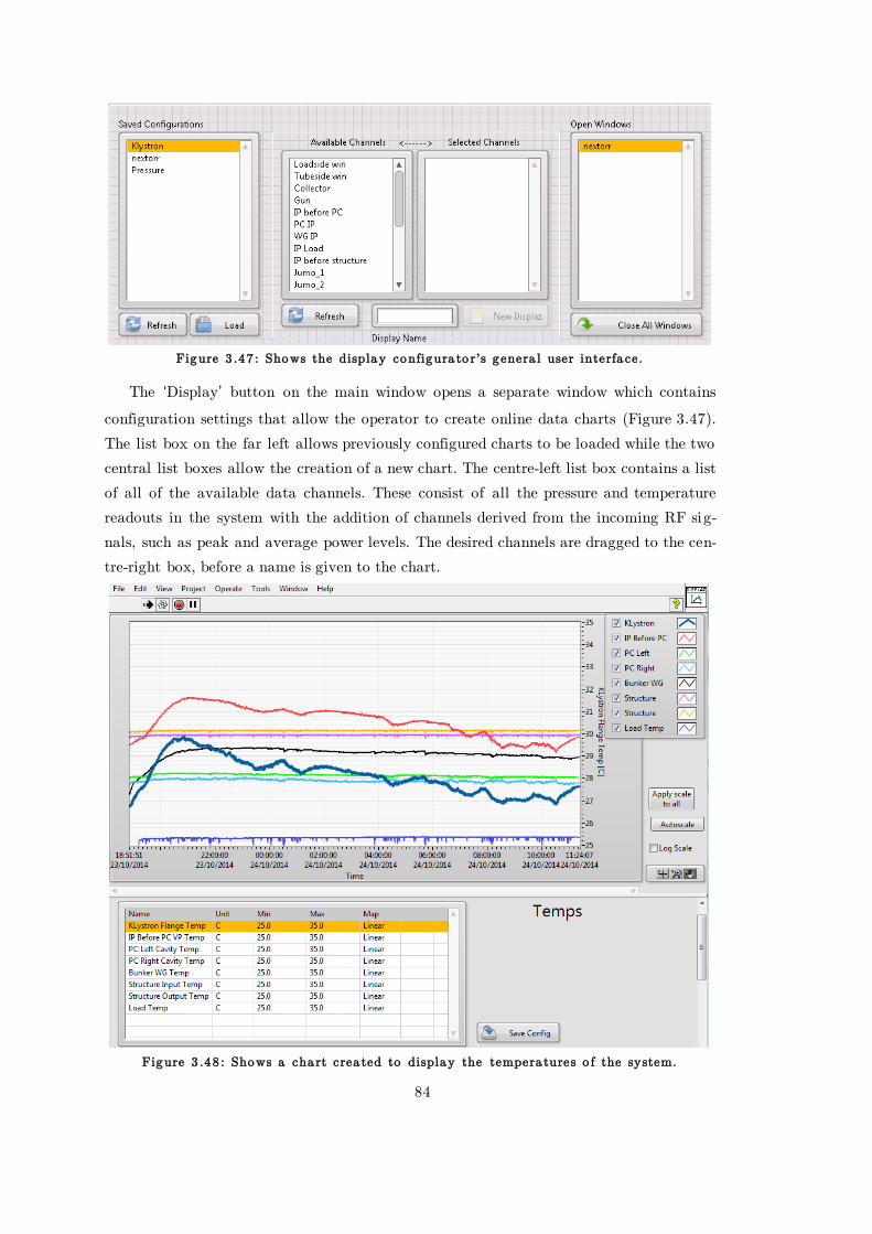
84
Figure 3 .47 : Shows the display configura to r's g enera l user interfa ce.
The ‘Display’ button on the main window opens a separate window which contains
configuration settings that allow the operator to create online data charts (Figure 3.47).
The list box on the far left allows previously configured charts to be loaded while the two
central list boxes allow the creation of a new chart. The centre-left list box contains a list
of all of the available data channels. These consist of all the pressure and temperature
readouts in the system with the addition of channels derived from the incoming RF sig-
nals, such as peak and average power levels. The desired channels are dragged to the cen-
tre-right box, before a name is given to the chart.
Figure 3 .48 : Shows a cha rt crea ted to display the tempera tures o f the system.
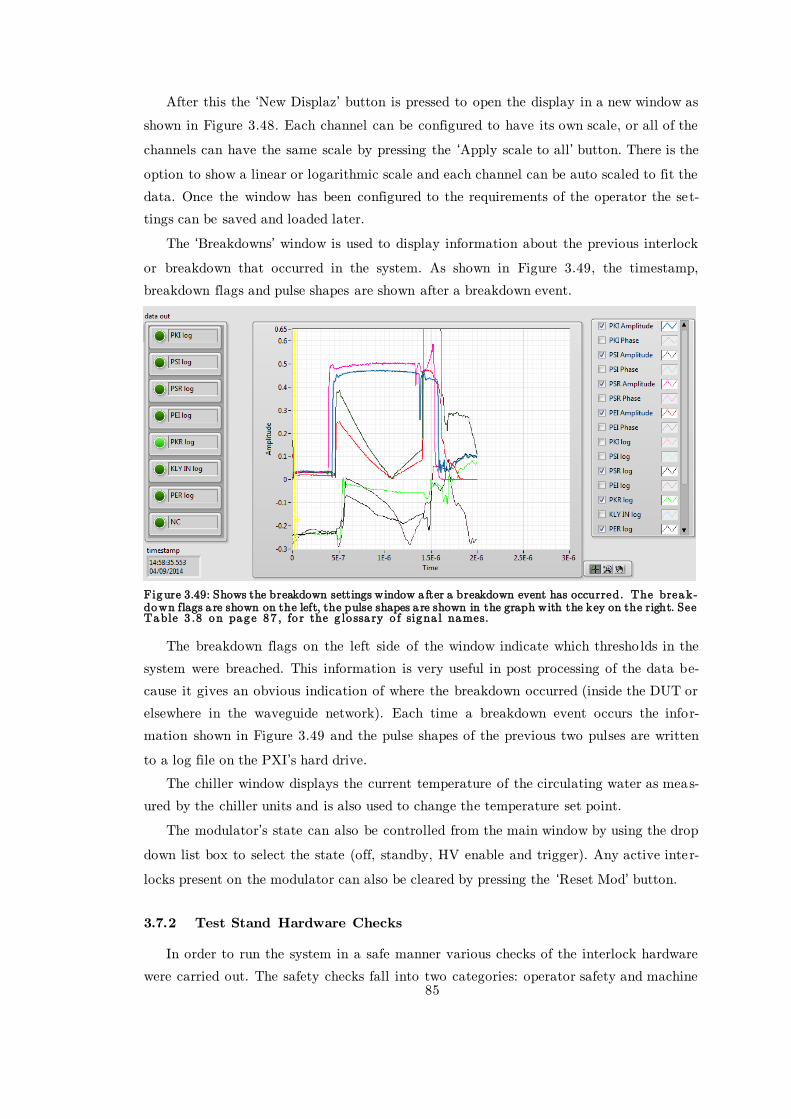
85
After this the ‘New Displaz’ button is pressed to open the display in a new window as
shown in Figure 3.48. Each channel can be configured to have its own scale, or all of the
channels can have the same scale by pressing the ‘Apply scale to all’ button. There is the
option to show a linear or logarithmic scale and each channel can be auto scaled to fit the
data. Once the window has been configured to the requirements of the operator the set-
tings can be saved and loaded later.
The ‘Breakdowns’ window is used to display information about the previous interlock
or breakdown that occurred in the system. As shown in Figure 3.49, the timestamp,
breakdown flags and pulse shapes are shown after a breakdown event.
Figure 3.49: Shows the breakdown settings window a fter a breakdown event has occurred. The brea k-down flags a re shown on the left, the pulse shapes a re shown in the graph with the key on the right. See Table 3 .8 on page 87 , fo r the g lo ssa ry o f signa l names.
The breakdown flags on the left side of the window indicate which thresho lds in the
system were breached. This information is very useful in post processing of the data be-
cause it gives an obvious indication of where the breakdown occurred (inside the DUT or
elsewhere in the waveguide network). Each time a breakdown event occurs the infor-
mation shown in Figure 3.49 and the pulse shapes of the previous two pulses are written
to a log file on the PXI’s hard drive.
The chiller window displays the current temperature of the circulating water as meas-
ured by the chiller units and is also used to change the temperature set point.
The modulator’s state can also be controlled from the main window by using the drop
down list box to select the state (off, standby, HV enable and trigger). Any active inter-
locks present on the modulator can also be cleared by pressing the ‘Reset Mod’ button.
3.7.2 Test Stand Hardware Checks
In order to run the system in a safe manner various checks of the interlock hardware
were carried out. The safety checks fall into two categories: operator safety and machine
86
safety. The risks to the operator include high power RF, high voltage and X-ray radiation
exposure. To mitigate these risks the affected areas are made to be inaccessible while the
modulator is pulsing. This is achieved through the use of electromechanical switches at-
tached to the access doors, which in turn are wired to the modulator ’s interlock system
(see section 3.6.5 for more information). Before pulsing the system at full power these in-
terlock systems were checked by opening the access doors while pulsing the modulator at
0 V.
The risks to the machine hardware mainly come from bad vacuum integrity and RF
reflection. The pressure inside the waveguides is monitored by the vacuum gauges and ion
pump controllers, which are connected to the modulator’s and PXI’s interlock systems via
contact relays. These systems were first tested by switching off each vacuum controller in
isolation to see if the PXI and modulator systems interlocked. To test if breaching the
pressure set point activated the interlocks the pressure set points were decreased manua l-
ly to be lower than the ambient pressure level on each controller. Both of these tests were
successful in interlocking the modulator and PXI crate.
In order to test the RF interlocks RF power was injected from a function generator
and the log detector thresholds lowered until the system interlocked. The same procedure
was conducted in the PXI software to test the ADC/FPGA based interlock threshold de-
tection. The interlock thresholds were approached from above and below to test both in-
terlock directions. To fully verify that the interlocks on the PXI were effective, the LLRF
output was monitored to ensure the RF signal was terminated when the software’s inter-
lock indicator was active.
The final check that was made before RF power was activated was a visual inspection
of the RF gate valves in the waveguide network. The valves have a pneumatic piston to
open/close the device, but the compressed air installation was not finished at the time.
Remote, electronic control of the valves had also not been completed such that the only
way to know if the valves were open or closed was a visual inspection. A closed RF valve
would work as a short circuit causing 100 % reflection back to the klystron, putting at a
high risk of damage.
3.7.3 RF Cable Calibration
At Xbox-2 the RF signals are sent from the directional couplers to the LLRF rack via
long coaxial cables. These cables need to have their insertion loss measured and calibra t-
ed. This was achieved by unscrewing the RF cables from the directional couplers and in-
jecting RF power using an Anritsu MG3692C signal generator. The power output of the
generator was measured using a Rohde & Schwarz NRP-Z81 power sensor and NRP-2
base unit. At the LLRF rack end of the cable the power was measured through the 8:1
RF multiplexer with the permanently installed power meter as described in 3.3.7. This set
up increases precision because only one end of the cable needs to be disturbed. The differ-
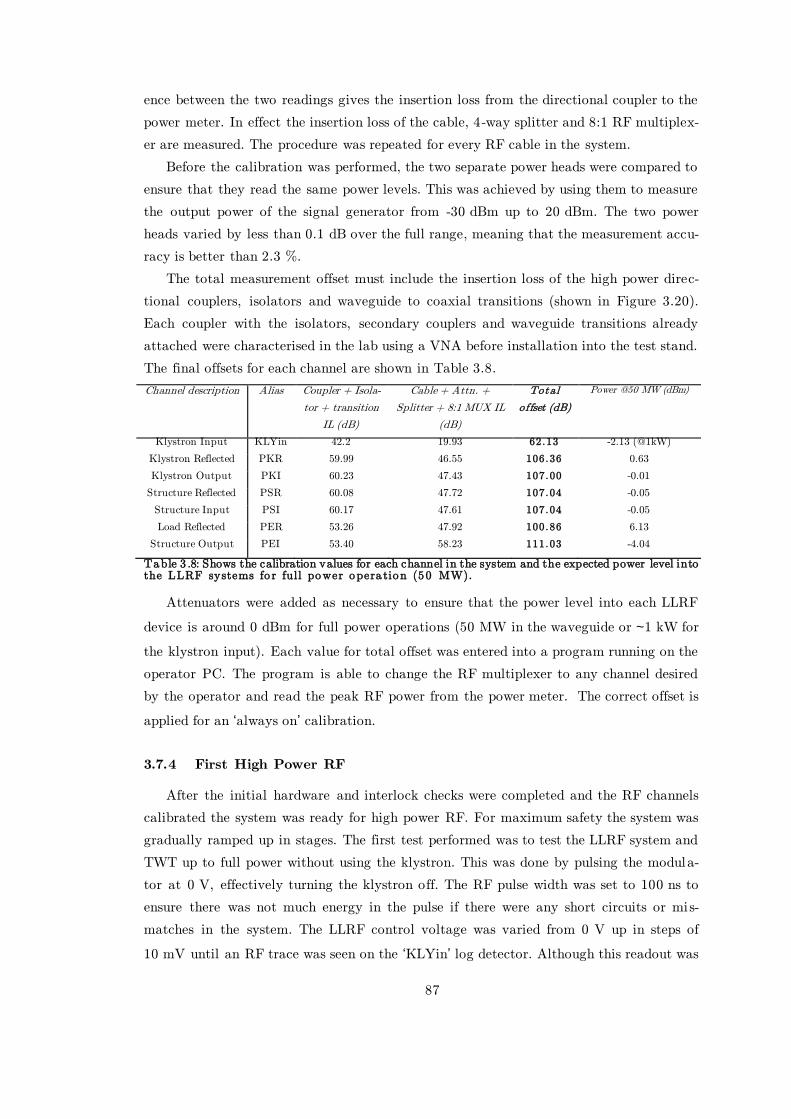
87
ence between the two readings gives the insertion loss from the directional coupler to the
power meter. In effect the insertion loss of the cable, 4-way splitter and 8:1 RF multiplex-
er are measured. The procedure was repeated for every RF cable in the system.
Before the calibration was performed, the two separate power heads were compared to
ensure that they read the same power levels. This was achieved by using them to measure
the output power of the signal generator from -30 dBm up to 20 dBm. The two power
heads varied by less than 0.1 dB over the full range, meaning that the measurement accu-
racy is better than 2.3 %.
The total measurement offset must include the insertion loss of the high power direc-
tional couplers, isolators and waveguide to coaxial transitions (shown in Figure 3.20).
Each coupler with the isolators, secondary couplers and waveguide transitions already
attached were characterised in the lab using a VNA before installation into the test stand.
The final offsets for each channel are shown in Table 3.8.
Channel description Alias Coupler + Isola-
tor + transition
IL (dB)
Cable + Attn. +
Splitter + 8:1 MUX IL
(dB)
Total
offset (dB)
Power @50 MW (dBm)
Klystron Input KLYin 42.2 19.93 62.13 -2.13 (@1kW)
Klystron Reflected PKR 59.99 46.55 106.36 0.63
Klystron Output PKI 60.23 47.43 107.00 -0.01
Structure Reflected PSR 60.08 47.72 107.04 -0.05
Structure Input PSI 60.17 47.61 107.04 -0.05
Load Reflected PER 53.26 47.92 100.86 6.13
Structure Output PEI 53.40 58.23 111.03 -4.04
Table 3 .8: Shows the calibration values for each channel in the system and the expected power level into the LLRF systems fo r full power opera tion (50 MW).
Attenuators were added as necessary to ensure that the power level into each LLRF
device is around 0 dBm for full power operations (50 MW in the waveguide or ~1 kW for
the klystron input). Each value for total offset was entered into a program running on the
operator PC. The program is able to change the RF multiplexer to any channel desired
by the operator and read the peak RF power from the power meter. The correct offset is
applied for an ‘always on’ calibration.
3.7.4 First High Power RF
After the initial hardware and interlock checks were completed and the RF channels
calibrated the system was ready for high power RF. For maximum safety the system was
gradually ramped up in stages. The first test performed was to test the LLRF system and
TWT up to full power without using the klystron. This was done by pulsing the modula-
tor at 0 V, effectively turning the klystron off. The RF pulse width was set to 100 ns to
ensure there was not much energy in the pulse if there were any short circuits or mis-
matches in the system. The LLRF control voltage was varied from 0 V up in steps of
10 mV until an RF trace was seen on the ‘KLYin’ log detector. Although this readout was
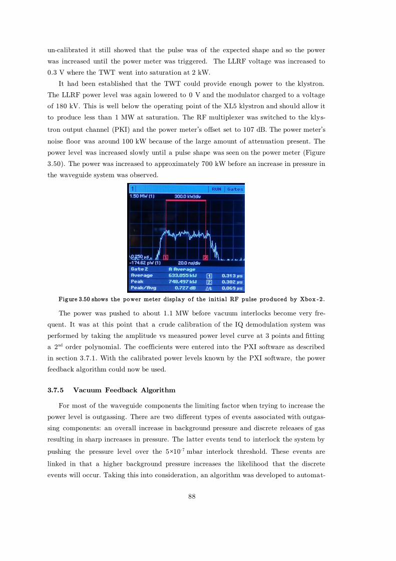
88
un-calibrated it still showed that the pulse was of the expected shape and so the power
was increased until the power meter was triggered. The LLRF voltage was increased to
0.3 V where the TWT went into saturation at 2 kW.
It had been established that the TWT could provide enough power to the klystron.
The LLRF power level was again lowered to 0 V and the modulator charged to a voltage
of 180 kV. This is well below the operating point of the XL5 klystron and should allow it
to produce less than 1 MW at saturation. The RF multiplexer was switched to the klys-
tron output channel (PKI) and the power meter’s offset set to 107 dB. The power meter’s
noise floor was around 100 kW because of the large amount of attenuation present. The
power level was increased slowly until a pulse shape was seen on the power meter (Figure
3.50). The power was increased to approximately 700 kW before an increase in pressure in
the waveguide system was observed.
Figure 3.50 shows the power meter display o f the initia l RF pulse produced by Xbox -2 .
The power was pushed to about 1.1 MW before vacuum interlocks become very fre-
quent. It was at this point that a crude calibration of the IQ demodulation system was
performed by taking the amplitude vs measured power level curve at 3 points and fitting
a 2nd order polynomial. The coefficients were entered into the PXI software as described
in section 3.7.1. With the calibrated power levels known by the PXI software, the power
feedback algorithm could now be used.
3.7.5 Vacuum Feedback Algorithm
For most of the waveguide components the limiting factor when trying to increase the
power level is outgassing. There are two different types of events associated with outgas-
sing components: an overall increase in background pressure and discrete releases of gas
resulting in sharp increases in pressure. The latter events tend to interlock the system by
pushing the pressure level over the 5×10⁻⁷ mbar interlock threshold. These events are
linked in that a higher background pressure increases the likelihood that the discrete
events will occur. Taking this into consideration, an algorithm was developed to automat-

89
ically change the power level depending on the background pressure and the rate at which
vacuum interlocks occur.
The vacuum feedback loop consists of a PID loop that uses the pressure level as the
process variable and the RF power level as the input variable. If the vacuum level is in-
creasing the power level will decrease in order to compensate and vice versa. The most
important terms used in the PID loop are the proportional and differential parts. The in-
tegral part is not so important because the exact value of the pressure set point is not as
important as the fast reaction to vacuum events. The proportional gain is adjusted such
that the power level would react in a stable manner to the background changes in pres-
sure level. For a stable feedback loop the proportional term should be of the same order
of magnitude as the inverse of the process variable. Since the pressure level is typically 10 -
9 mbar, initially the gain was set at 109. It was later adjusted to 4×10¹⁰ because the power
feedback algorithm was too slow in reacting to the power level change as requested by the
pressure feedback loop.
The differential gain responds to fast changes in pressure such as those caused by the
discrete outgassing events. The PXI software reads the pressure level every second, during
which the pressure level can increase by more than 2 orders of magnitude during some
vacuum events. For this reason the differential gain was first set to 0.02, and then low-
ered to 0.001 as the feedback loop was overcompensating for the vacuum spikes.
The second part of the algorithm responded to vacuum interlocks when the pressure
increased above the 5×10⁻⁷ mbar threshold. A user defined power was subtracted from the
power set point after every event (typically 20-50 kW) and the power level capped at the
new value for 60 seconds. This had the effect that if there were clusters of vacuum events
the power level would decrease until the system stabilised.
As shown in Figure 3.51, the pressure level remains constant while the power level in-
creases over time. The process variable used was the ‘IP Load’ pressure, which had a set
point of 1.2×10⁻⁷ mbar. It denotes the pressure level as measured by the ion pump at-
tached to the high power stainless steel load. During initial conditioning this component
undergoes the highest outgassing because most of the RF energy is dissipated here
through ohmic heating. It was for this reason that this channel was chosen for use in the
feedback loop. However, the channel used can be changed in the software if a component
started to outgas more heavily than the load.
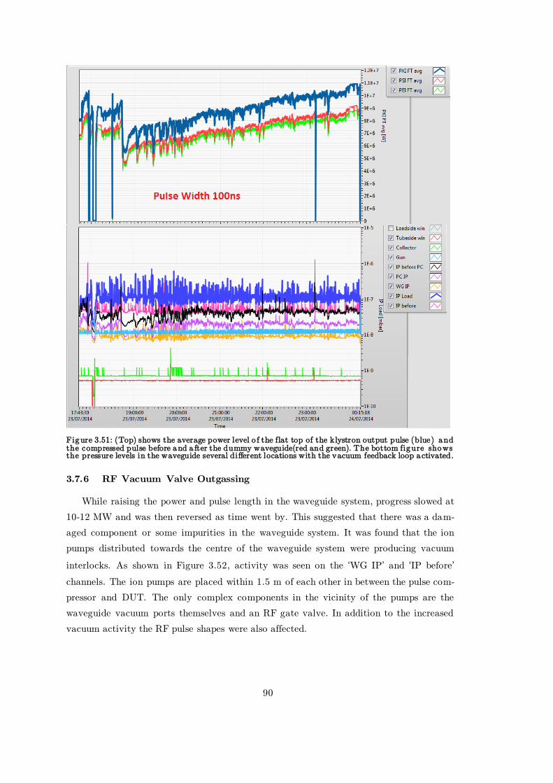
90
Figure 3.51: (Top) shows the average power level o f the flat top of the klystron output pulse (blue) and the compressed pulse before and a fter the dummy waveguide(red and green). The bottom figure shows the pressure levels in the waveguide several different locations with the vacuum feedback loop a ctivated.
3.7.6 RF Vacuum Valve Outgassing
While raising the power and pulse length in the waveguide system, progress slowed at
10-12 MW and was then reversed as time went by. This suggested that there was a dam-
aged component or some impurities in the waveguide system. It was found that the ion
pumps distributed towards the centre of the waveguide system were producing vacuum
interlocks. As shown in Figure 3.52, activity was seen on the ‘WG IP’ and ‘IP before’
channels. The ion pumps are placed within 1.5 m of each other in between the pulse com-
pressor and DUT. The only complex components in the vicinity of the pumps are the
waveguide vacuum ports themselves and an RF gate valve. In addition to the increased
vacuum activity the RF pulse shapes were also affected.
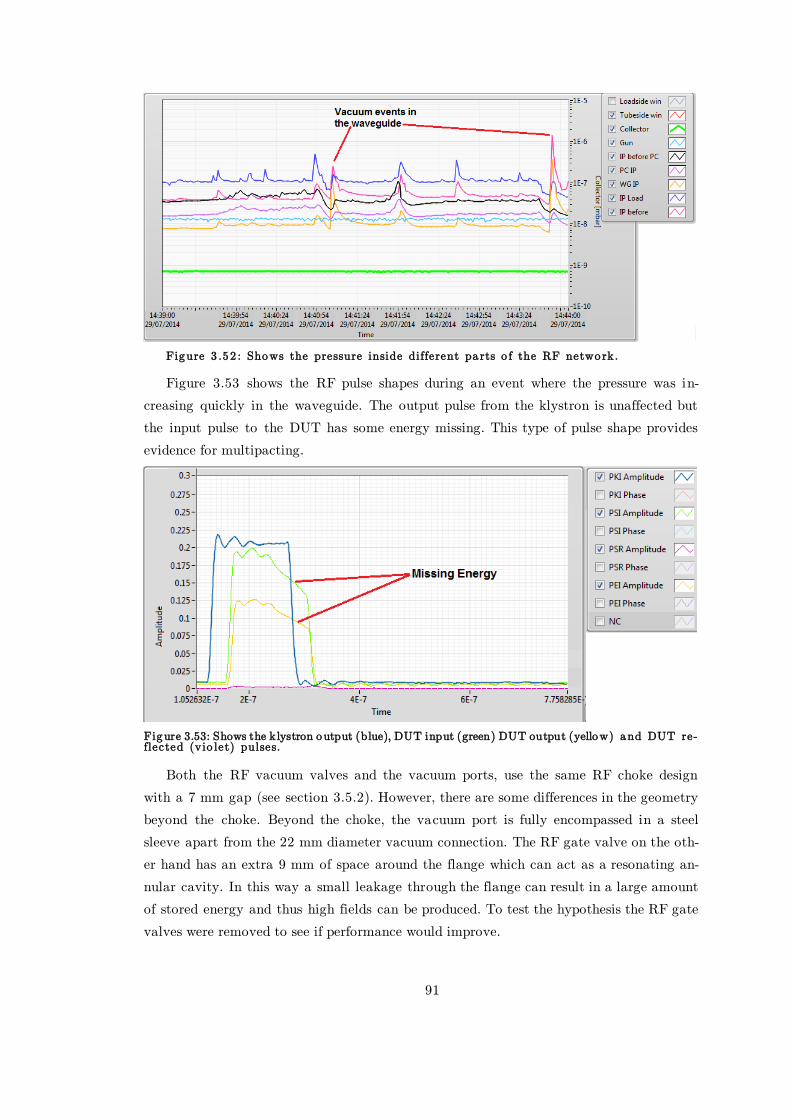
91
Figure 3 .52 : Shows the pressure inside different pa rts o f the RF network.
Figure 3.53 shows the RF pulse shapes during an event where the pressure was in-
creasing quickly in the waveguide. The output pulse from the klystron is unaffected but
the input pulse to the DUT has some energy missing. This type of pulse shape provides
evidence for multipacting.
Figure 3.53: Shows the klystron output (blue), DUT input (green) DUT output (yellow) and DUT re-flected (vio let) pulses.
Both the RF vacuum valves and the vacuum ports, use the same RF choke design
with a 7 mm gap (see section 3.5.2). However, there are some differences in the geometry
beyond the choke. Beyond the choke, the vacuum port is fully encompassed in a steel
sleeve apart from the 22 mm diameter vacuum connection. The RF gate valve on the oth-
er hand has an extra 9 mm of space around the flange which can act as a resonating an-
nular cavity. In this way a small leakage through the flange can result in a large amount
of stored energy and thus high fields can be produced. To test the hypothesis the RF gate
valves were removed to see if performance would improve.
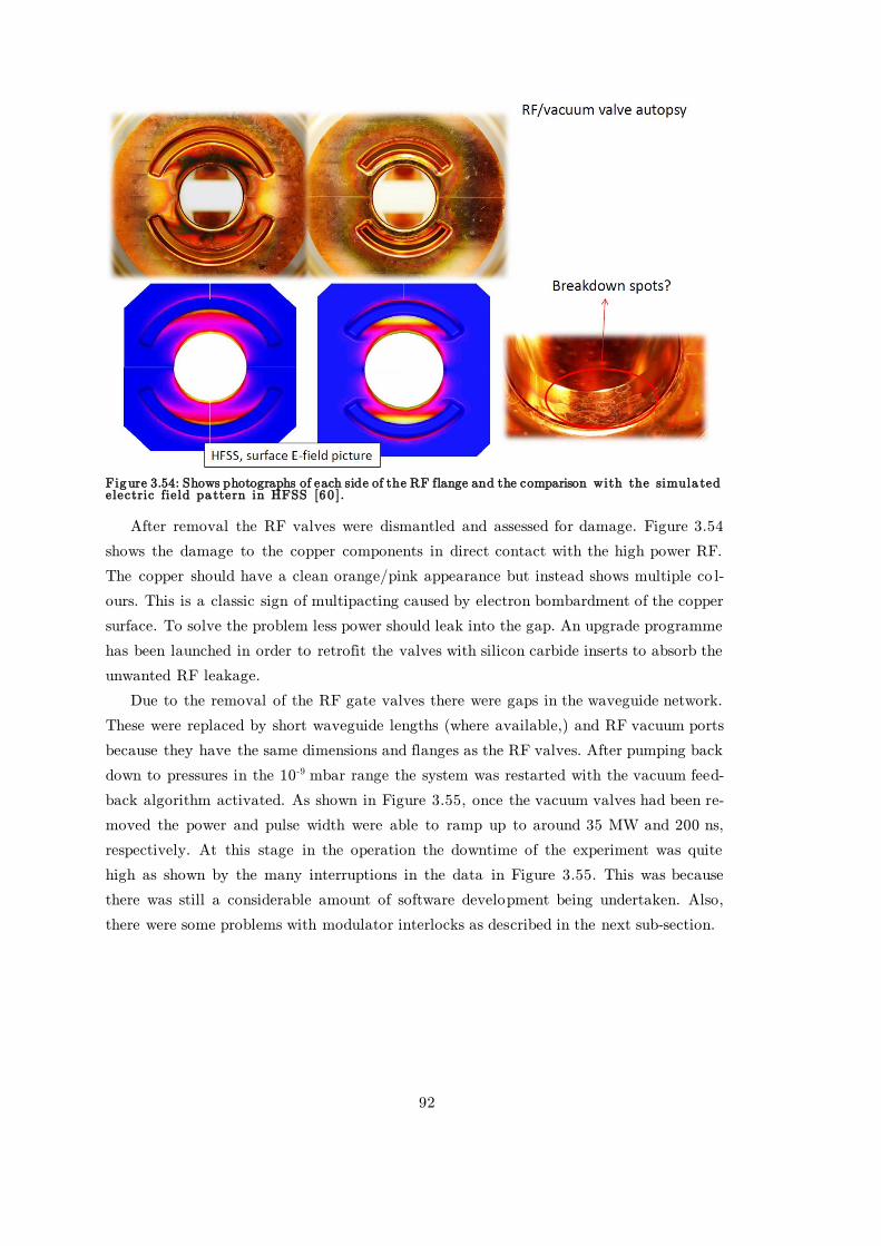
92
Figure 3.54: Shows photographs of each side of the RF flange and the comparison with the simula ted electric fie ld pa ttern in HFSS [60 ].
After removal the RF valves were dismantled and assessed for damage. Figure 3.54
shows the damage to the copper components in direct contact with the high power RF.
The copper should have a clean orange/pink appearance but instead shows multiple co l-
ours. This is a classic sign of multipacting caused by electron bombardment of the copper
surface. To solve the problem less power should leak into the gap. An upgrade programme
has been launched in order to retrofit the valves with silicon carbide inserts to absorb the
unwanted RF leakage.
Due to the removal of the RF gate valves there were gaps in the waveguide network.
These were replaced by short waveguide lengths (where available,) and RF vacuum ports
because they have the same dimensions and flanges as the RF valves. After pumping back
down to pressures in the 10-9 mbar range the system was restarted with the vacuum feed-
back algorithm activated. As shown in Figure 3.55, once the vacuum valves had been re-
moved the power and pulse width were able to ramp up to around 35 MW and 200 ns,
respectively. At this stage in the operation the downtime of the experiment was quite
high as shown by the many interruptions in the data in Figure 3.55. This was because
there was still a considerable amount of software development being undertaken. Also,
there were some problems with modulator interlocks as described in the next sub-section.
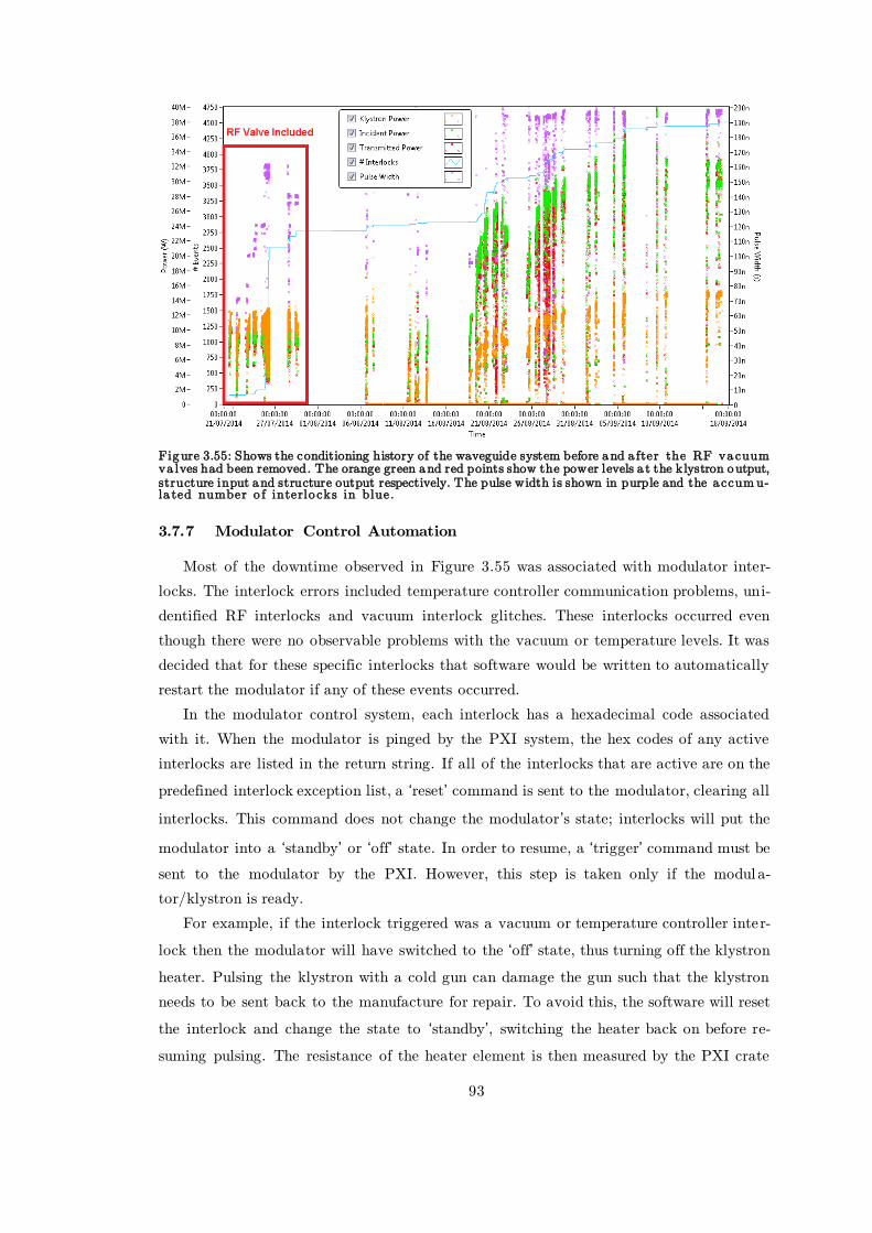
93
Figure 3.55: Shows the conditioning history of the waveguide system before and a fter the RF vacuum va lves had been removed. The orange green and red points show the power levels a t the klystron output, structure input and structure output respectively. The pulse width is shown in purple and the a ccum u-la ted number o f interlo cks in blue.
3.7.7 Modulator Control Automation
Most of the downtime observed in Figure 3.55 was associated with modulator inter-
locks. The interlock errors included temperature controller communication problems, uni-
dentified RF interlocks and vacuum interlock glitches. These interlocks occurred even
though there were no observable problems with the vacuum or temperature levels. It was
decided that for these specific interlocks that software would be written to automatically
restart the modulator if any of these events occurred.
In the modulator control system, each interlock has a hexadecimal code associated
with it. When the modulator is pinged by the PXI system, the hex codes of any active
interlocks are listed in the return string. If all of the interlocks that are active are on the
predefined interlock exception list, a ‘reset’ command is sent to the modulator, clearing all
interlocks. This command does not change the modulator’s state; interlocks will put the
modulator into a ‘standby’ or ‘off’ state. In order to resume, a ‘trigger’ command must be
sent to the modulator by the PXI. However, this step is taken only if the modul a-
tor/klystron is ready.
For example, if the interlock triggered was a vacuum or temperature controller inter-
lock then the modulator will have switched to the ‘off’ state, thus turning off the klystron
heater. Pulsing the klystron with a cold gun can damage the gun such that the klystron
needs to be sent back to the manufacture for repair. To avoid this, the software will reset
the interlock and change the state to ‘standby’, switching the heater back on before re-
suming pulsing. The resistance of the heater element is then measured by the PXI crate

94
to ensure that the klystron gun is back up to full temperature. Once the klystron is back
up to temperature triggering is resumed and the PXI interlocks are reset to re-establish
the trigger signal.
3.8 Conclusion
This chapter described much of the development conducted in order to build a second
klystron based, X-band, high power test stand at CERN. The increased testing capacity
allows more performance data to be collected for new high gradient accelerating structure
designs. The results can be used to make informed choices when designing the next gener-
ation of accelerating structures and to test new theories trying to explain breakdown
mechanisms.
We developed a new LLRF system to improve the accuracy and speed at which data
could be collected compared to Xbox-1. A combination of logarithmic detectors and direct
digital sampling were used to provide large dynamic range, robust interlocking and more
precise phase and amplitude measurements. A PXI based acquisition system was used
with FPGA based interlocking and IQ demodulation. All interlock control was performed
by the PXI crate or by the modulator control system.
New waveguide components were designed which were more compact than previously
tested versions. These included directional couplers, vacuum ports, vacuum valves and a
new pulse compressor. All of the new components were manufactured and cold tested be-
fore installation. Commissioning of the test stand has been completed up to a peak power
of 35 MW and all control systems and interlocks validated.
95
Chapter 4
4 Xbox-3
4.1 Further Increase of Test Capacity with Reduced Cost
Xbox-3 is the third X-band test stand to be built at CERN and approaches the prob-
lem of achieving a high peak power at 12 GHz in a novel fashion. As discussed the XL4/5
type klystrons used in the Xbox, SLAC and KEK test stands are state of the art devices
and thus expensive. The high cost is due to the high voltages used, increasing the com-
plexity of the klystron and modulator. In order to reduce cost the voltage can be lowered,
but this also decreases the peak power output. The average power output can remain the
same however, by increasing the pulse repetition rate. Peak power levels are recovered by
combing the output power of multiple klystrons and through pulse compression. This pro-
cess allows the production of 50 MW, 200-300 ns pulses at much higher repetition rates
than would be possible with a single XL5 klystron.
4.2 RF Combination Scheme
The type of combination scheme required to reach the 50 MW, 300 ns pulse needed
depends on the klystron’s RF specification. Based on frequency scaling of klystrons that
were already available on the market, it was decided that a klystron with a peak power of
6 MW and pulse length of 4-5 𝜇s should be able to be built by industry. Toshiba accepted
the tender to build a klystron with the required parameters and a pulse repetition rate of
400 Hz. From these specifications the peak power should be increased by a factor of 9 -10
in order to produce at least 50 MW and include overhead for waveguide network power
losses. Pulse compression can reliably provide power multiplication up to 4 times when
compressing a 4 𝜇s pulse down to 300 ns. The extra factor of 2.5 can be provided by
combing 3 or more klystrons.
A further consideration concerns the repetition rate and thus the high average power
of the system. At 400 Hz repetition rate, 300 ns pulse width and 50 MW peak power the
average power is 6 kW. CLIC accelerating structures are not designed to deal with such
high average power levels and could suffer damage if these pulses were applied. The aver-
age power can be reduced by lowering the repetition rate to 100 Hz. This means that with
the correct combination scheme 4 structures can be tested at the same time using 400 Hz
power sources. Figure 4.1 shows how such a scheme can be realised.
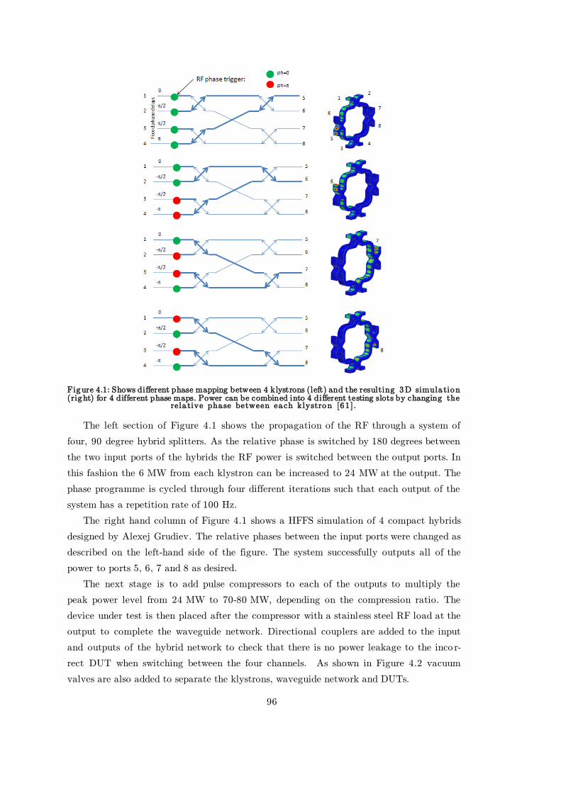
96
Figure 4.1: Shows different phase mapping between 4 klystrons (left) and the resulting 3D simula tion (right) for 4 different phase maps. Power can be combined into 4 different testing slots by changing the
rela tive phase between each klystron [61 ].
The left section of Figure 4.1 shows the propagation of the RF through a system of
four, 90 degree hybrid splitters. As the relative phase is switched by 180 degrees between
the two input ports of the hybrids the RF power is switched between the output ports. In
this fashion the 6 MW from each klystron can be increased to 24 MW at the output. The
phase programme is cycled through four different iterations such that each output of the
system has a repetition rate of 100 Hz.
The right hand column of Figure 4.1 shows a HFFS simulation of 4 compact hybrids
designed by Alexej Grudiev. The relative phases between the input ports were changed as
described on the left-hand side of the figure. The system successfully outputs all of the
power to ports 5, 6, 7 and 8 as desired.
The next stage is to add pulse compressors to each of the outputs to multiply the
peak power level from 24 MW to 70-80 MW, depending on the compression ratio. The
device under test is then placed after the compressor with a stainless steel RF load at the
output to complete the waveguide network. Directional couplers are added to the input
and outputs of the hybrid network to check that there is no power leakage to the inco r-
rect DUT when switching between the four channels. As shown in Figure 4.2 vacuum
valves are also added to separate the klystrons, waveguide network and DUTs.
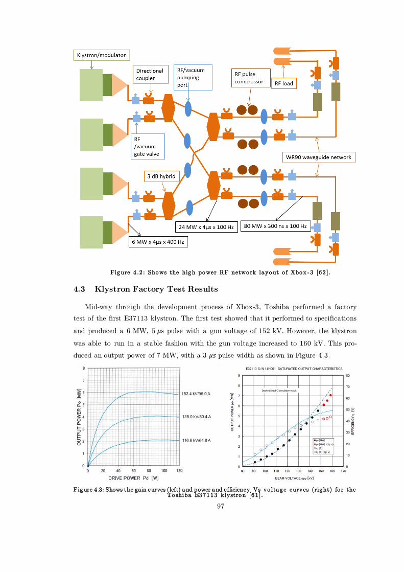
97
Figure 4 .2 : Shows the high power RF network layout o f Xbox -3 [62 ].
4.3 Klystron Factory Test Results
Mid-way through the development process of Xbox-3, Toshiba performed a factory
test of the first E37113 klystron. The first test showed that it performed to specifications
and produced a 6 MW, 5 𝜇s pulse with a gun voltage of 152 kV. However, the klystron
was able to run in a stable fashion with the gun voltage increased to 160 kV. This pro-
duced an output power of 7 MW, with a 3 𝜇𝑠 pulse width as shown in Figure 4.3.
Figure 4.3: Shows the gain curves (left) and power and efficiency Vs vo ltage curves (right) fo r the Toshiba E37113 klystron [61 ].

98
Although the peak power output is only 1 MW higher than expected, it requires that
the waveguide layout is revisited. The original layout is capable of producing 80 MW
pulses at 300 ns. This is far higher than the 45-50 MW required to test unloaded, CLIC
prototype structures. The high power level was due to the fact that factor 4 pulse com-
pression was used and 4 klystrons were combined. With 7 MW available it is possible to
combine only twice and compress 4 times to reach 56 MW (neglecting waveguide losses),
which is a gain of 8 MW compared to a 6 MW klystron. With this improvement, 4 devic-
es can be tested at 200 Hz each, again doubling the testing capacity. Compared to the
current set-up of Xbox-1 and 2, which operate one structure at a repetition rate of 50 Hz,
the capacity is boosted by a factor of 16.
Figure 4.4 shows an updated layout of Xbox-3’s waveguide network. Two hybrids
have been removed, in effect creating two separate test stands. Each combines power
from two klystrons and alternates power between two DUTs.
Figure 4.4: Shows the updated layout o f Xbox-3 with the a cquired channels indicated by co loured a r-rows. The Faraday cup signals (orange), waveguide network reflected/interlock signals (red), DUT sig -na ls (blue) and waveguide diagnostic/ fo rward signa ls (g reen) signa ls a re shown.
Each different type of channel as indicated in Figure 4.4 will have a separate LLRF
subsystem. For all reflected signals that are essential for machine protection and inter-
locking, log detectors will be used because a phase measurement is not needed. For signals
surrounding the DUT (blue arrows), high bandwidth phase and amplitude measurements
are required. The 400 MHz IF scheme using the NI 5772 digitisers will be used as de-
scribed in section 3.3.
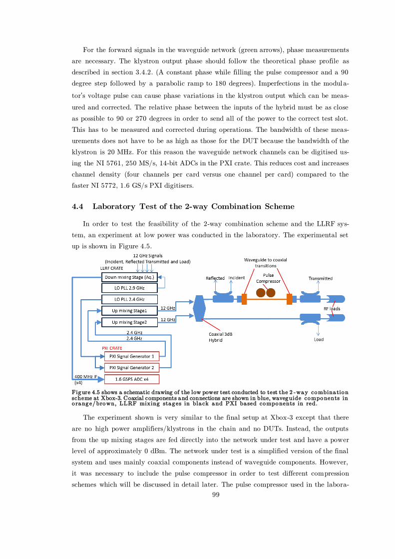
99
For the forward signals in the waveguide network (green arrows), phase measurements
are necessary. The klystron output phase should follow the theoretical phase profile as
described in section 3.4.2. (A constant phase while filling the pulse compressor and a 90
degree step followed by a parabolic ramp to 180 degrees). Imperfections in the modula-
tor’s voltage pulse can cause phase variations in the klystron output which can be meas-
ured and corrected. The relative phase between the inputs of the hybrid must be as close
as possible to 90 or 270 degrees in order to send all of the power to the correct test slot.
This has to be measured and corrected during operations. The bandwidth of these meas-
urements does not have to be as high as those for the DUT because the bandwidth of the
klystron is 20 MHz. For this reason the waveguide network channels can be digitised us-
ing the NI 5761, 250 MS/s, 14-bit ADCs in the PXI crate. This reduces cost and increases
channel density (four channels per card versus one channel per card) compared to the
faster NI 5772, 1.6 GS/s PXI digitisers.
4.4 Laboratory Test of the 2-way Combination Scheme
In order to test the feasibility of the 2-way combination scheme and the LLRF sys-
tem, an experiment at low power was conducted in the laboratory. The experimental set
up is shown in Figure 4.5.
Figure 4.5 shows a schematic drawing of the low power test conducted to test the 2 -way combina tion scheme at Xbox-3. Coaxial components and connections are shown in blue, waveguide components in o range/brown, LLRF mixing stages in bla ck and PXI ba sed components in red.
The experiment shown is very similar to the final setup at Xbox-3 except that there
are no high power amplifiers/klystrons in the chain and no DUTs. Instead, the outputs
from the up mixing stages are fed directly into the network under test and have a power
level of approximately 0 dBm. The network under test is a simplified version of the final
system and uses mainly coaxial components instead of waveguide components. However,
it was necessary to include the pulse compressor in order to test different compression
schemes which will be discussed in detail later. The pulse compressor used in the labora-

100
tory test was the Xbox-2 pulse compressor. This is designed to compress a 1.5 𝜇s pulse
down to 250 ns with a compression ratio of 3. Because of the shorter pulse compared with
Xbox-3 the filling time of the Xbox-2 pulse compressor is on the order of 650 ns. Howev-
er, for Xbox-3 the pulse compressor’s coupling coefficient will be modified to increase the
filling time to a couple of microseconds. This increases the compression efficiency for the
longer pulse lengths that will be used at Xbox-3 of 3-5 𝜇s.
Two vector modulated signals are produced at 2.4 GHz using two NI 5793 PXI RF
transmitter modules, which are then up-mixed using a modified version of the Xbox-2
mixing crate. The two signals are then fed into the 3 dB, 90º coaxial hybrid. Connected
to one the first hybrid output is a coaxial directional coupler, which in turn is connected
to a coaxial to waveguide transition. The transition is then connected directly to the
Xbox-2 pulse compressor after which there is a transition back to coaxial with a final di-
rectional coupler and termination. At the second output there is just one directional cou-
pler and a termination. The signals from the directional couplers are fed into a 4 channel
down mixing system and acquired by the high speed PXI ADCs.
The purpose of the experiment is to show that the two signal generators can be
properly combined using the hybrid to produce the required modulated pulse for the pulse
compressor. It must be such that a good flat output pulse is produced. This can be
achieved by either varying the input phase of the pulse compressor as described in previ-
ous sections, or by modulating the input amplitude to the pulse compressor. The second
verification is that by changing the relative phase between the two generators, power can
be sent to the second hybrid output with minimal power leakage to the first output. The
final test is to ensure that the power can be switched reliably between each output at a
rate of 200 times per second.
There are two ways to produce a flat output pulse from a SLED I pulse compressor;
by phase modulation as described in section 2.2.3 or by amplitude modulation. When the
input power to a filled pulse compressor is turned off, the cavities empty with an expo-
nential decay, with a time constant related to the filling time. This decay can be stopped
by switching back on the input power and ramping up the amplitude in an exponential
fashion in order to counteract the decay at the output. The pulse shape is a standard rec-
tangular pulse with a missing shark fin shaped notch at the end. An advantage of this
method is that the output phase of the pulse compressor is constant over the entire pulse,
which is favourable for operation with beam. A second advantage is that the flatness of
the output pulse is less dependent on the resonant frequency of the cavity, because the
pulse flatness is produced by an amplitude variation and not a phase variation in time
(which is essentially a frequency chirp). The main disadvantage is that the compression
efficiency is reduced, which could be an issue at Xbox-3 because there is not a large over-
head in the amount of power available from the klystrons.
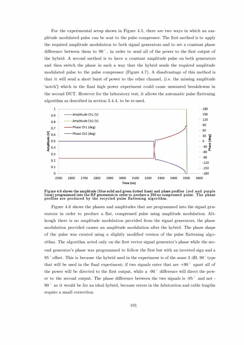
101
For the experimental setup shown in Figure 4.5, there are two ways in which an am-
plitude modulated pulse can be sent to the pulse compressor. The first method is to apply
the required amplitude modulation to both signal generators and to set a constant phase
difference between them to 90º, in order to send all of the power to the first output of
the hybrid. A second method is to have a constant amplitude pulse on both generators
and then switch the phase in such a way that the hybrid sends the required amplitude
modulated pulse to the pulse compressor (Figure 4.7). A disadvantage of this method is
that it will send a short burst of power to the other channel, (i.e. the missing amplitude
‘notch’) which in the final high power experiment could cause unwanted breakdowns in
the second DUT. However for the laboratory test, it allows the automatic pulse flattening
algorithm as described in section 3.4.4, to be re-used.
Figure 4.6 shows the amplitude (blue solid and green dotted lines) and phase profiles (red and purple lines) programmed into the RF generators in order to produce a 250 ns compressed pulse. The phase pro files a re produced by the recycled pulse fla ttening a lgo rithm.
Figure 4.6 shows the phases and amplitudes that are programmed into the signal gen-
erators in order to produce a flat, compressed pulse using amplitude modulation. Alt-
hough there is no amplitude modulation provided from the signal generators, the phase
modulation provided causes an amplitude modulation after the hybrid. The phase shape
of the pulse was created using a slightly modified version of the pulse flattening algo-
rithm. The algorithm acted only on the first vector signal generator ’s phase while the sec-
ond generator’s phase was programmed to follow the first but with an inverted sign and a
95ºoffset. This is because the hybrid used in the experiment is of the same 3 dB, 90ºtype
that will be used in the final experiment; if two signals enter that are +90º apart all of
the power will be directed to the first output, while a -90º difference will direct the pow-
er to the second output. The phase difference between the two signals is -95º and not -
90º as it would be for an ideal hybrid, because errors in the fabrication and cable lengths
require a small correction.
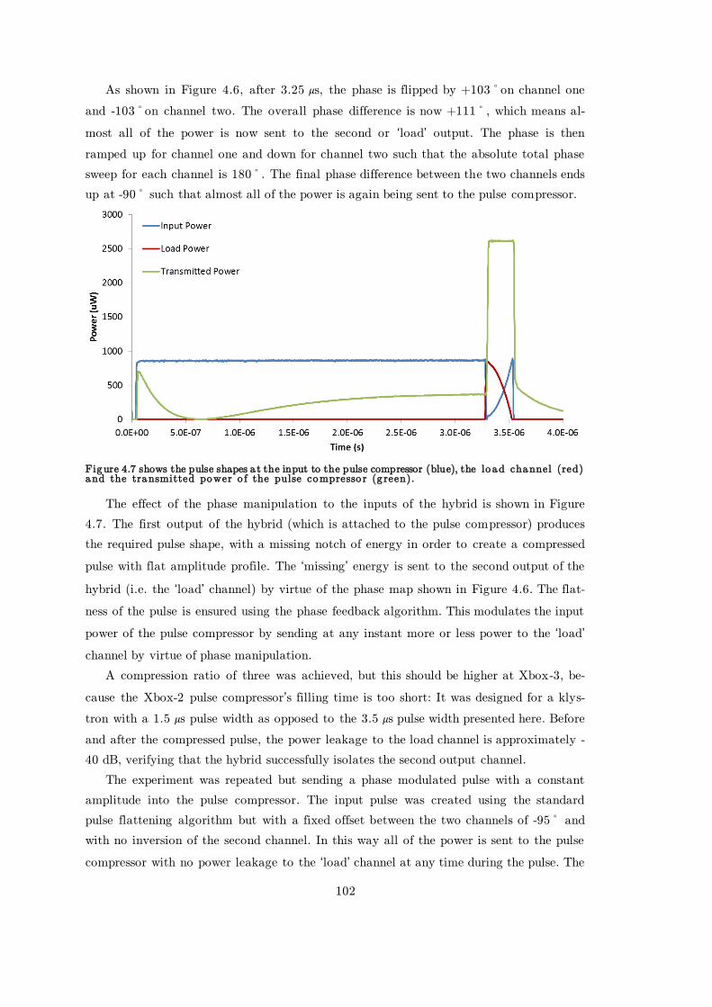
102
As shown in Figure 4.6, after 3.25 𝜇s, the phase is flipped by +103ºon channel one
and -103ºon channel two. The overall phase difference is now +111º, which means al-
most all of the power is now sent to the second or ‘load’ output. The phase is then
ramped up for channel one and down for channel two such that the absolute total phase
sweep for each channel is 180º. The final phase difference between the two channels ends
up at -90º such that almost all of the power is again being sent to the pulse compressor.
Figure 4.7 shows the pulse shapes a t the input to the pulse compressor (blue), the load channel (red) and the transmitted power o f the pulse compresso r (g reen).
The effect of the phase manipulation to the inputs of the hybrid is shown in Figure
4.7. The first output of the hybrid (which is attached to the pulse compressor) produces
the required pulse shape, with a missing notch of energy in order to create a compressed
pulse with flat amplitude profile. The ‘missing’ energy is sent to the second output of the
hybrid (i.e. the ‘load’ channel) by virtue of the phase map shown in Figure 4.6. The flat-
ness of the pulse is ensured using the phase feedback algorithm. This modulates the input
power of the pulse compressor by sending at any instant more or less power to the ‘load’
channel by virtue of phase manipulation.
A compression ratio of three was achieved, but this should be higher at Xbox-3, be-
cause the Xbox-2 pulse compressor’s filling time is too short: It was designed for a klys-
tron with a 1.5 𝜇s pulse width as opposed to the 3.5 𝜇s pulse width presented here. Before
and after the compressed pulse, the power leakage to the load channel is approximately -
40 dB, verifying that the hybrid successfully isolates the second output channel.
The experiment was repeated but sending a phase modulated pulse with a constant
amplitude into the pulse compressor. The input pulse was created using the standard
pulse flattening algorithm but with a fixed offset between the two channels of -95º and
with no inversion of the second channel. In this way all of the power is sent to the pulse
compressor with no power leakage to the ‘load’ channel at any time during the pulse. The
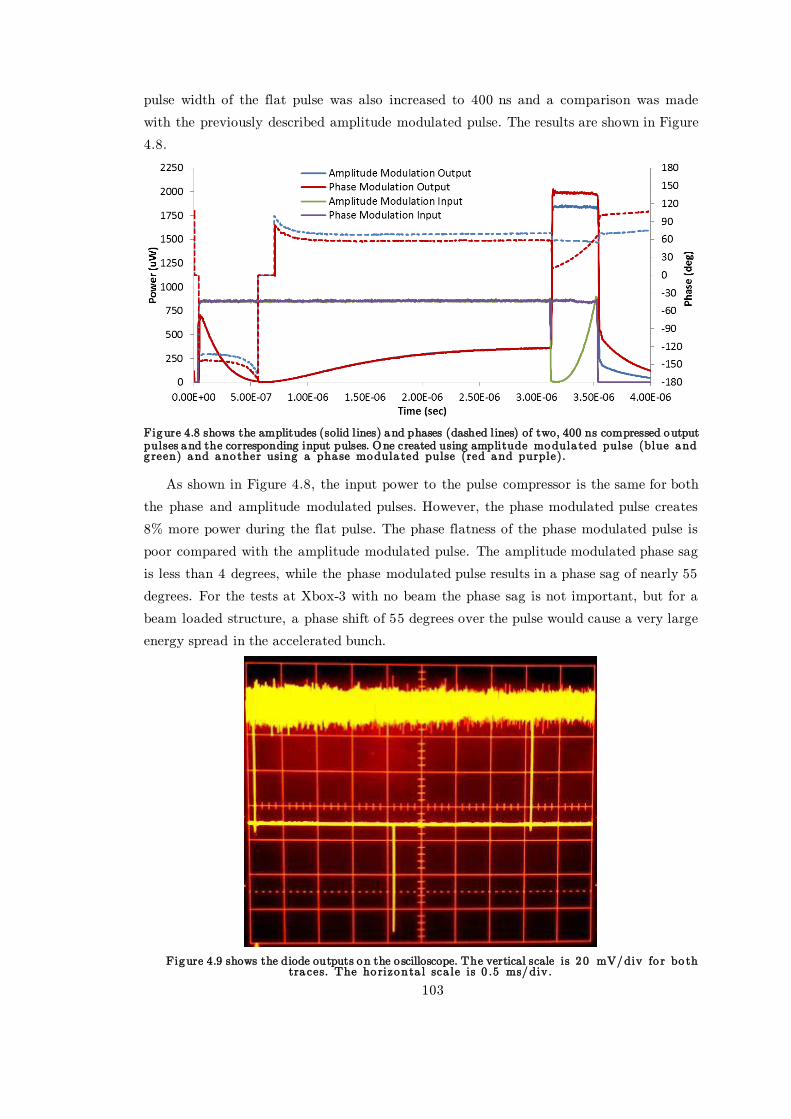
103
pulse width of the flat pulse was also increased to 400 ns and a comparison was made
with the previously described amplitude modulated pulse. The results are shown in Figure
4.8.
Figure 4.8 shows the amplitudes (solid lines) and phases (dashed lines) of two, 400 ns compressed output pulses and the corresponding input pulses. One created using amplitude modula ted pulse (blue and g reen) and ano ther using a phase modula ted pulse (red and purple).
As shown in Figure 4.8, the input power to the pulse compressor is the same for both
the phase and amplitude modulated pulses. However, the phase modulated pulse creates
8% more power during the flat pulse. The phase flatness of the phase modulated pulse is
poor compared with the amplitude modulated pulse. The amplitude modulated phase sag
is less than 4 degrees, while the phase modulated pulse results in a phase sag of nearly 55
degrees. For the tests at Xbox-3 with no beam the phase sag is not important, but for a
beam loaded structure, a phase shift of 55 degrees over the pulse would cause a very large
energy spread in the accelerated bunch.
Figure 4.9 shows the diode outputs on the o scilloscope. The vertical scale is 20 mV/div fo r bo th tra ces. The ho rizonta l sca le is 0 .5 ms/div.
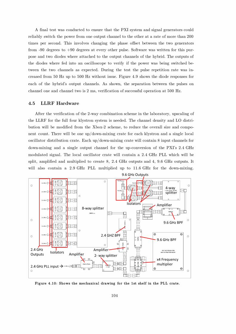
104
A final test was conducted to ensure that the PXI system and signal generators could
reliably switch the power from one output channel to the other at a rate of more than 200
times per second. This involves changing the phase offset between the two generators
from -90 degrees to +90 degrees at every other pulse. Software was written for this pur-
pose and two diodes where attached to the output channels of the hybrid. The outputs of
the diodes where fed into an oscilloscope to verify if the power was being switched be-
tween the two channels as expected. During the test the pulse repetition rate was in-
creased from 50 Hz up to 500 Hz without issue. Figure 4.9 shows the diode responses for
each of the hybrid’s output channels. As shown, the separation between the pulses on
channel one and channel two is 2 ms, verification of successful operation at 500 Hz.
4.5 LLRF Hardware
After the verification of the 2-way combination scheme in the laboratory, upscaling of
the LLRF for the full four klystron system is needed. The channel density and LO distri-
bution will be modified from the Xbox-2 scheme, to reduce the overall size and compo-
nent count. There will be one up/down-mixing crate for each klystron and a single local
oscillator distribution crate. Each up/down-mixing crate will contain 8 input channels for
down-mixing and a single output channel for the up-conversion of the PXI’s 2.4 GHz
modulated signal. The local oscillator crate will contain a 2.4 GHz PLL which will be
split, amplified and multiplied to create 8, 2.4 GHz outputs and 4, 9.6 GHz outputs. It
will also contain a 2.9 GHz PLL multiplied up to 11.6 GHz for the down-mixing.
Figure 4 .10 : Shows the mechanica l drawing fo r the 1 st shelf in the PLL cra te.
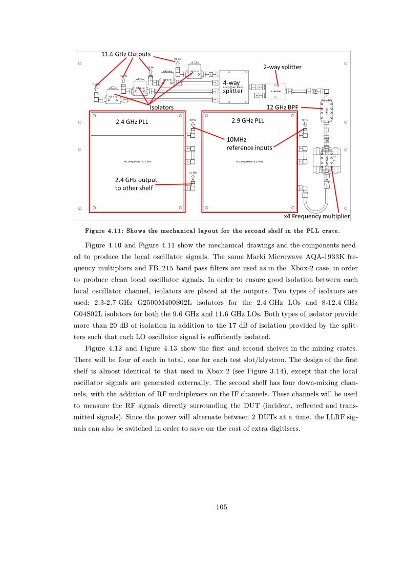
105
Figure 4 .11 : Shows the mechanica l layout fo r the second shelf in the PLL cra te.
Figure 4.10 and Figure 4.11 show the mechanical drawings and the components need-
ed to produce the local oscillator signals. The same Marki Microwave AQA-1933K fre-
quency multipliers and FB1215 band pass filters are used as in the Xbox-2 case, in order
to produce clean local oscillator signals. In order to ensure good isolation between each
local oscillator channel, isolators are placed at the outputs. Two types of isolators are
used: 2.3-2.7 GHz G2500M400S02L isolators for the 2.4 GHz LOs and 8-12.4 GHz
G04S02L isolators for both the 9.6 GHz and 11.6 GHz LOs. Both types of isolator provide
more than 20 dB of isolation in addition to the 17 dB of isolation provided by the split-
ters such that each LO oscillator signal is sufficiently isolated.
Figure 4.12 and Figure 4.13 show the first and second shelves in the mixing crates.
There will be four of each in total, one for each test slot/klystron. The design of the first
shelf is almost identical to that used in Xbox-2 (see Figure 3.14), except that the local
oscillator signals are generated externally. The second shelf has four down-mixing chan-
nels, with the addition of RF multiplexers on the IF channels. These channels will be used
to measure the RF signals directly surrounding the DUT (incident, reflected and trans-
mitted signals). Since the power will alternate between 2 DUTs at a time, the LLRF sig-
nals can also be switched in order to save on the cost of extra digitisers.
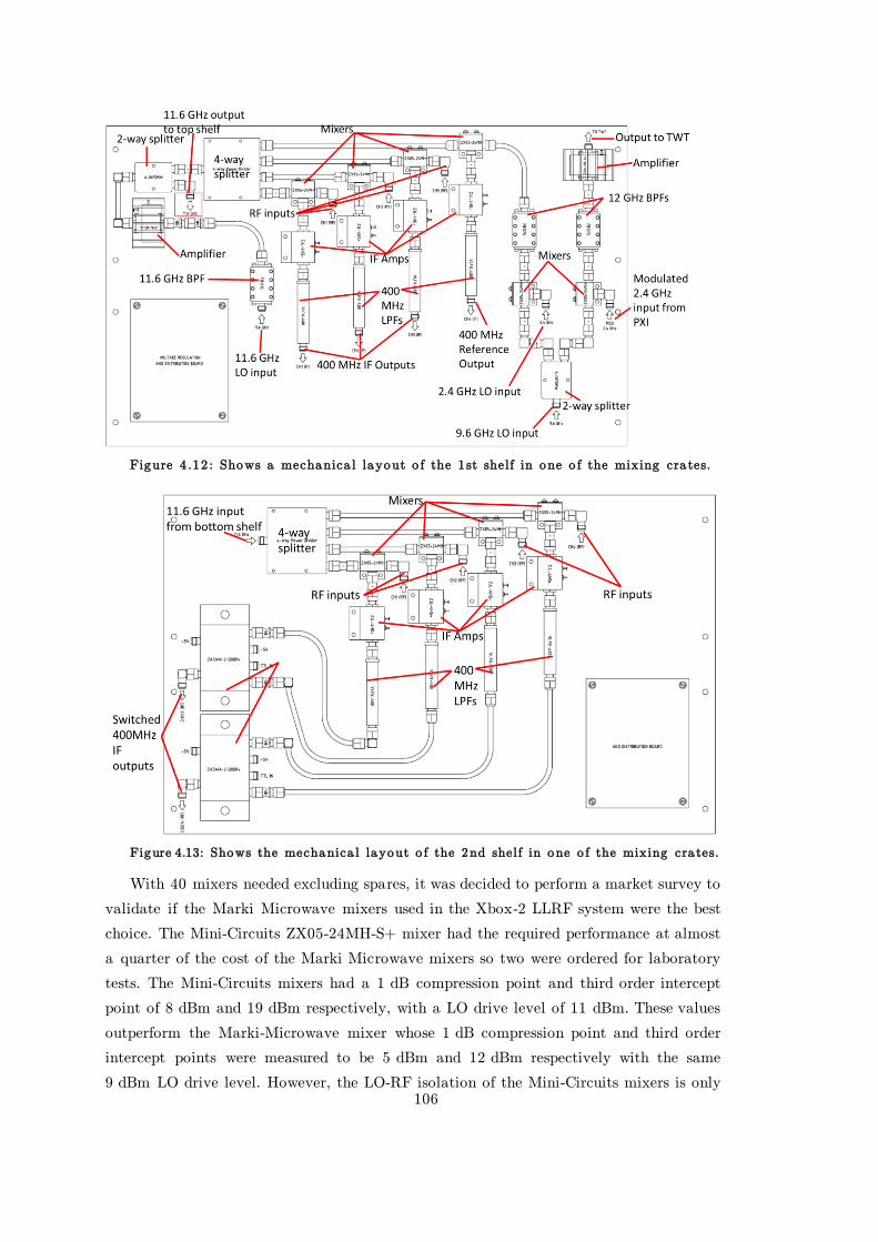
106
Figure 4 .12 : Shows a mechanica l layout o f the 1 st shelf in one o f the mixing cra tes.
Figure 4.13: Shows the mechanica l layout o f the 2nd shelf in one o f the mixing cra tes.
With 40 mixers needed excluding spares, it was decided to perform a market survey to
validate if the Marki Microwave mixers used in the Xbox-2 LLRF system were the best
choice. The Mini-Circuits ZX05-24MH-S+ mixer had the required performance at almost
a quarter of the cost of the Marki Microwave mixers so two were ordered for laboratory
tests. The Mini-Circuits mixers had a 1 dB compression point and third order intercept
point of 8 dBm and 19 dBm respectively, with a LO drive level of 11 dBm. These values
outperform the Marki-Microwave mixer whose 1 dB compression point and third order
intercept points were measured to be 5 dBm and 12 dBm respectively with the same
9 dBm LO drive level. However, the LO-RF isolation of the Mini-Circuits mixers is only
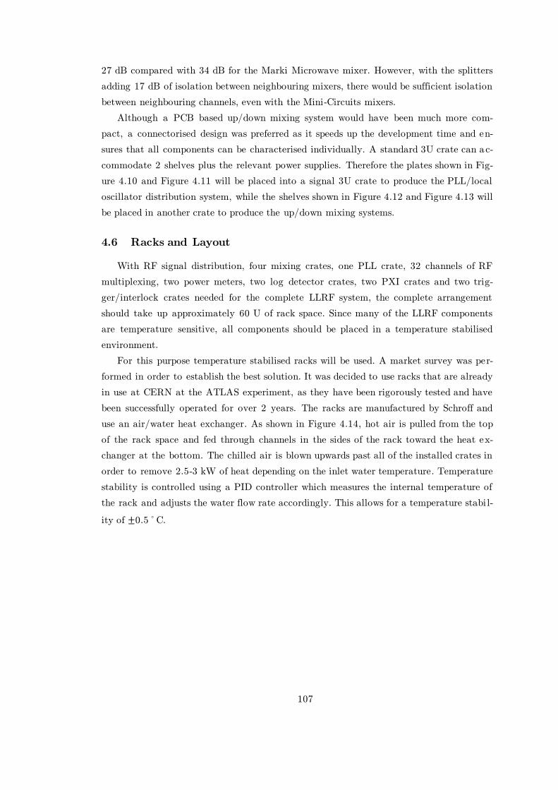
107
27 dB compared with 34 dB for the Marki Microwave mixer. However, with the splitters
adding 17 dB of isolation between neighbouring mixers, there would be sufficient isolation
between neighbouring channels, even with the Mini-Circuits mixers.
Although a PCB based up/down mixing system would have been much more com-
pact, a connectorised design was preferred as it speeds up the development time and en-
sures that all components can be characterised individually. A standard 3U crate can a c-
commodate 2 shelves plus the relevant power supplies. Therefore the plates shown in Fig-
ure 4.10 and Figure 4.11 will be placed into a signal 3U crate to produce the PLL/local
oscillator distribution system, while the shelves shown in Figure 4.12 and Figure 4.13 will
be placed in another crate to produce the up/down mixing systems.
4.6 Racks and Layout
With RF signal distribution, four mixing crates, one PLL crate, 32 channels of RF
multiplexing, two power meters, two log detector crates, two PXI crates and two trig-
ger/interlock crates needed for the complete LLRF system, the complete arrangement
should take up approximately 60 U of rack space. Since many of the LLRF components
are temperature sensitive, all components should be placed in a temperature stabilised
environment.
For this purpose temperature stabilised racks will be used. A market survey was per-
formed in order to establish the best solution. It was decided to use racks that are already
in use at CERN at the ATLAS experiment, as they have been rigorously tested and have
been successfully operated for over 2 years. The racks are manufactured by Schroff and
use an air/water heat exchanger. As shown in Figure 4.14, hot air is pulled from the top
of the rack space and fed through channels in the sides of the rack toward the heat ex-
changer at the bottom. The chilled air is blown upwards past all of the installed crates in
order to remove 2.5-3 kW of heat depending on the inlet water temperature. Temperature
stability is controlled using a PID controller which measures the internal temperature of
the rack and adjusts the water flow rate accordingly. This allows for a temperature stabi l-
ity of ±0.5ºC.

108
Figure 4.14 shows a schematic drawing of the rack cooling circuit (left) and a photograph o f the empty ra ck (right).
It is important to consider the layout of both racks for cable management purposes.
Xbox-3 has a 2x2 test slot layout; each pair of klystrons are separated and have their own
fully independent control system. The crates installed into the racks reflect this, with
each rack being a mirror of the other, apart from the local oscillator distribution (or PLL)
crate, which distributes signals to both of the Xbox-3 sub-systems.
As in Xbox-2 the RF signal cables from the experiment will approach the crate at a
height of approximately 2.5 m. A rectangular hole at the top of the rack containing a
piece of foam with a slit brings in the signal cables and stops the chilled air from escap-
ing. The RF distribution crate is placed at the top of the rack and contains 2-way split-
ters which send each signal to a LLRF diagnostic crate (for down-mixing or log detection)
and to the calibration system. All 12 GHz signal distribution will use the same high sta-
bility Killer BeeTM cables as used in Xbox-2.
Located immediately below the RF distribution crate are the crates which make up
the calibration system. They are placed there to keep cable lengths as short as possible
for the calibration path. Like Xbox-2, the calibration system uses RF multiplexers and
power meters. However, because of the increased channel density a network of multiplex-
ers will be used as shown in Figure 4.15.
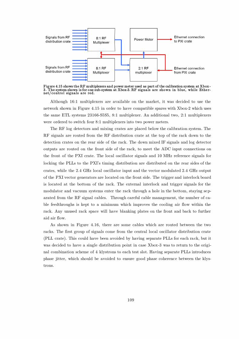
109
Figure 4.15 shows the RF multiplexers and power meter used as part of the calibration system at Xbox -3 . The system shown is for one sub-system at Xbox-3. RF signa ls a re shown in blue, while Ethe r-net/contro l signa ls a re red.
Although 16:1 multiplexers are available on the market, it was decided to use the
network shown in Figure 4.15 in order to have compatible spares with Xbox-2 which uses
the same ETL systems 23166-S5S5, 8:1 multiplexer. An additional two, 2:1 multiplexers
were ordered to switch four 8:1 multiplexers into two power meters.
The RF log detectors and mixing crates are placed below the calibration system. The
RF signals are routed from the RF distribution crate at the top of the rack down to the
detection crates on the rear side of the rack. The down mixed IF signals and log detector
outputs are routed on the front side of the rack, to meet the ADC input connections on
the front of the PXI crate. The local oscillator signals and 10 MHz reference signals for
locking the PLLs to the PXI’s timing distribution are distributed on the rear sides of the
crates, while the 2.4 GHz local oscillator input and the vector modulated 2.4 GHz output
of the PXI vector generators are located on the front side. The trigger and interlock board
is located at the bottom of the rack. The external interlock and trigger signals for the
modulator and vacuum systems enter the rack through a hole in the bottom, staying sep-
arated from the RF signal cables. Through careful cable management, the number of ca-
ble feedthroughs is kept to a minimum which improves the cooling air flow within the
rack. Any unused rack space will have blanking plates on the front and back to further
aid air flow.
As shown in Figure 4.16, there are some cables which are routed between the two
racks. The first group of signals come from the central local oscillator distribution crate
(PLL crate). This could have been avoided by having separate PLLs for each rack, but it
was decided to have a single distribution point in case Xbox-3 was to return to the origi-
nal combination scheme of 4 klystrons to each test slot. Having separate PLLs introduces
phase jitter, which should be avoided to ensure good phase coherence between the klys-
trons.
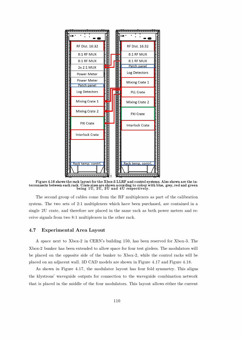
110
Figure 4.16 shows the rack layout for the Xbox-3 LLRF and control systems. Also shown a re the in-terconnects between each rack. Crate sizes are shown according to colour with blue, grey, red and g reen
being 1U, 2U, 3U and 4U respectively.
The second group of cables come from the RF multiplexers as part of the calibration
system. The two sets of 2:1 multiplexers which have been purchased, are contained in a
single 2U crate, and therefore are placed in the same rack as both power meters and re-
ceive signals from two 8:1 multiplexers in the other rack.
4.7 Experimental Area Layout
A space next to Xbox-2 in CERN’s building 150, has been reserved for Xbox-3. The
Xbox-2 bunker has been extended to allow space for four test girders. The modulators will
be placed on the opposite side of the bunker to Xbox-2, while the control racks will be
placed on an adjacent wall. 3D CAD models are shown in Figure 4.17 and Figure 4.18.
As shown in Figure 4.17, the modulator layout has four fold symmetry. This aligns
the klystrons’ waveguide outputs for connection to the waveguide combination network
that is placed in the middle of the four modulators. This layout allows either the current
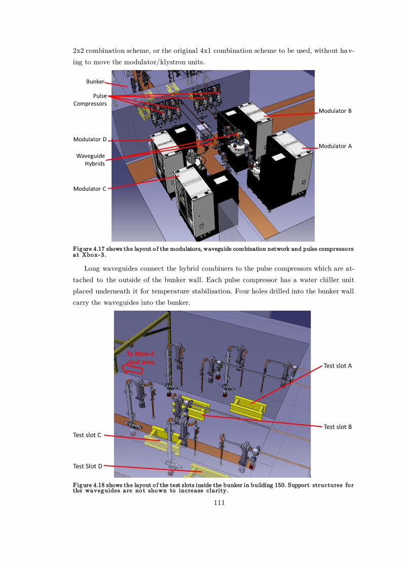
111
2x2 combination scheme, or the original 4x1 combination scheme to be used, without hav-
ing to move the modulator/klystron units.
Figure 4.17 shows the layout o f the modulators, waveguide combination network and pulse compresso rs a t Xbox-3 .
Long waveguides connect the hybrid combiners to the pulse compressors which are at-
tached to the outside of the bunker wall. Each pulse compressor has a water chiller unit
placed underneath it for temperature stabilisation. Four holes drilled into the bunker wall
carry the waveguides into the bunker.
Figure 4.18 shows the layout o f the test slots inside the bunker in building 150. Support structures fo r the waveguides a re no t shown to increa se cla rity.
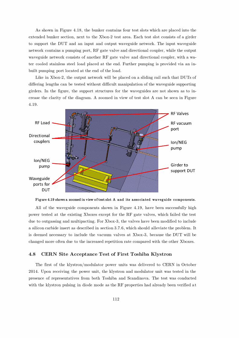
112
As shown in Figure 4.18, the bunker contains four test slots which are placed into the
extended bunker section, next to the Xbox-2 test area. Each test slot consists of a girder
to support the DUT and an input and output waveguide network. The input waveguide
network contains a pumping port, RF gate valve and directional coupler, while the output
waveguide network consists of another RF gate valve and directional coupler, with a wa-
ter cooled stainless steel load placed at the end. Further pumping is provided via an in-
built pumping port located at the end of the load.
Like in Xbox-2, the output network will be placed on a sliding rail such that DUTs of
differing lengths can be tested without difficult manipulation of the waveguide supporting
girders. In the figure, the support structures for the waveguides are not shown as to in-
crease the clarity of the diagram. A zoomed in view of test slot A can be seen in Figure
4.19.
Figure 4.19 shows a zoomed in view o f test slot A and its a sso cia ted waveguide components.
All of the waveguide components shown in Figure 4.19, have been successfully high
power tested at the existing Xboxes except for the RF gate valves, which failed the test
due to outgassing and multipacting. For Xbox-3, the valves have been modified to include
a silicon carbide insert as described in section 3.7.6, which should alleviate the problem. It
is deemed necessary to include the vacuum valves at Xbox-3, because the DUT will be
changed more often due to the increased repetition rate compared with the other Xboxes.
4.8 CERN Site Acceptance Test of First Toshiba Klystron
The first of the klystron/modulator power units was delivered to CERN in October
2014. Upon receiving the power unit, the klystron and modulator unit was tested in the
presence of representatives from both Toshiba and Scandinova. The test was conducted
with the klystron pulsing in diode mode as the RF properties had already been verified a t

113
the Toshiba factory in Japan [63]. The site test could only be passed once certain objec-
tives had been completed.
In order to verify the micro-perveance of the klystron, the cathode voltage and cur-
rent have to be measured. This is achieved by using a capacitive voltage divider and a
current transformer respectively, which are located on the high voltage side of the pulse
transformer. This produces results that are free of the parasitic inductive and capacitive
effects of the pulse transformer and tuning circuitry that is present on the low voltage
side of the transformer.
Figure 4.20 shows the klystron cathode voltage and current in blue and red respectively , a s mea s-ured by the capacitive voltage divider and current transformer on the high voltage side o f the curren t transfo rmer.
The capacitive voltage divider installed into the modulator tank has a ratio of 9264:1,
while the current transformer has a ratio of 10:1 [64]. In Figure 4.20, the measured volt-
age and current on the oscilloscope have been multiplied by their respective ratios in o r-
der to reproduce the true voltage and current present at the gun. The measured voltage
and current in the middle of the flat top pulse are -163 kV and 97 A respectively. This
gives a micro-perveance of 1.47, which is slightly lower than the expected 1.55, but within
the acceptable range. The pulse flatness is 0.5 % rms for both voltage and current. The
total droop for a 5 𝜇s pulse is 2.5 % for the voltage and 3.1 % for the current. However,
most of this contribution comes from the start and end of the pulse. If the pulse is short-
ened to 3.5 𝜇s, the droop improves to 1.9 % and 2.3 % for the voltage and current respec-
tively.
The modulator/klystron unit was then run at a pulse repetition rate of 400 Hz, non-
stop for 8 hours to verify the long term performance. Various safety checks of the inter-
lock system were also conducted including:
Tube vacuum level interlock
Water flow rate interlocks
Water temperature interlocks
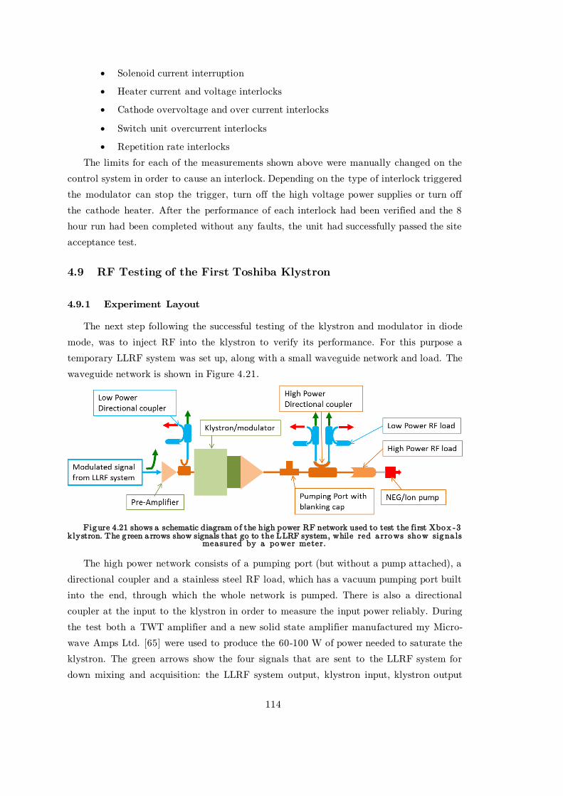
114
Solenoid current interruption
Heater current and voltage interlocks
Cathode overvoltage and over current interlocks
Switch unit overcurrent interlocks
Repetition rate interlocks
The limits for each of the measurements shown above were manually changed on the
control system in order to cause an interlock. Depending on the type of interlock triggered
the modulator can stop the trigger, turn off the high voltage power supplies or turn off
the cathode heater. After the performance of each interlock had been verified and the 8
hour run had been completed without any faults, the unit had successfully passed the site
acceptance test.
4.9 RF Testing of the First Toshiba Klystron
4.9.1 Experiment Layout
The next step following the successful testing of the klystron and modulator in diode
mode, was to inject RF into the klystron to verify its performance. For this purpose a
temporary LLRF system was set up, along with a small waveguide network and load. The
waveguide network is shown in Figure 4.21.
Figure 4.21 shows a schematic diagram o f the high power RF network used to test the first Xbox -3 klystron. The g reen a rrows show signals that go to the LLRF system, while red a rrows show signa ls
measured by a power meter.
The high power network consists of a pumping port (but without a pump attached), a
directional coupler and a stainless steel RF load, which has a vacuum pumping port built
into the end, through which the whole network is pumped. There is also a directional
coupler at the input to the klystron in order to measure the input power reliably. During
the test both a TWT amplifier and a new solid state amplifier manufactured my Micro-
wave Amps Ltd. [65] were used to produce the 60-100 W of power needed to saturate the
klystron. The green arrows show the four signals that are sent to the LLRF system for
down mixing and acquisition: the LLRF system output, klystron input, klystron output
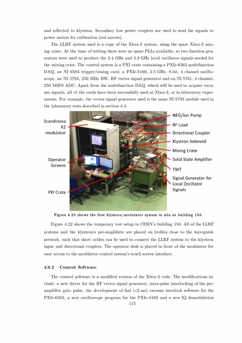
115
and reflected to klystron. Secondary low power couplers are used to send the signals to
power meters for calibration (red arrows).
The LLRF system used is a copy of the Xbox-2 system, using the spare Xbox-2 mix-
ing crate. At the time of writing there were no spare PLLs available, so two function gen-
erators were used to produce the 2.4 GHz and 2.9 GHz local oscillator signals needed for
the mixing crate. The control system is a PXI crate containing a PXIe-6363 multifunction
DAQ, an NI 6583 trigger/timing card, a PXIe-5160, 2.5 GHz, 8-bit, 4 channel oscillo-
scope, an NI 5793, 250 MHz BW, RF vector signal generator and an NI 5761, 4 channel,
250 MSPS ADC. Apart from the multifunction DAQ, which will be used to acquire vacu-
um signals, all of the cards have been successfully used at Xbox-2, or in laboratory exper-
iments. For example, the vector signal generator used is the same NI 5793 module used in
the laboratory tests described in section 4.4.
Figure 4 .22 shows the first k lystron/modula to r system in situ a t building 150 .
Figure 4.22 shows the temporary test setup in CERN’s building 150. All of the LLRF
systems and the klystron’s pre-amplifiers are placed on trollies close to the waveguide
network, such that short cables can be used to connect the LLRF system to the klystron
input and directional couplers. The operator desk is placed in front of the modulator for
easy access to the modulator control system’s touch screen interface.
4.9.2 Control Software
The control software is a modified version of the Xbox-2 code. The modifications in-
clude: a new driver for the RF vector signal generator, intra-pulse interlocking of the pre-
amplifier gate pulse, the development of fast (<2 ms) vacuum interlock software for the
PXIe-6363, a new oscilloscope program for the PXIe-5160 and a new IQ demodulation

116
scheme for the 5761 ADCs. Many of these modifications were made as part of a collabora-
tion with SLAC; where a PXI crate has been installed with an Xbox derived control sys-
tem [66].
The intra-pulse interlocking has been made possible due to the fact that the software
based vector modulator PXI card used at Xbox-2 (the NI PXIe-5673E), has been replaced
with an FPGA based module; the NI 5793R.
Figure 4.23 shows the operation of the NI 5793R RF transmitter. The RF transmitter module hardware is shown in blue, the FPGA hardware in g reen and the backplane line in red.
The vector modulated output uses 16-bit DACs which run at a rate of 250 MHz. The
FPGA interfaces with the DACs using two 16-bit buses. In the FPGA logic there is an
AND gate on the bus lines, with an inverted input attached to a PXI back plane line. If
this line goes high the DACs will output 0 V and stop the RF signal. The threshold de-
tector that is present in the FPGA based NI 5761, 250 MHz ADC, works on a sample by
sample basis and writes to the backplane line if a single sample breaches the threshold.
Including all pipeline delays the response time from a threshold breach in the ADC, to
the termination of the RF is approximately 400 ns.
A second level of safety is incorporated, by using the klystron pre-amplifier. The pre-
amplifiers (either the TWT or solid state amplifier) use pulsed power supplies which are
controlled by an input gate pulse. The gate pulse is sent from the PXI timing card which
also has the same AND gate logic. The trigger inhibit signal is controlled by the same
backplane line that inhibits the vector generator.
At Xbox-2 the vacuum levels are read using an RS485 serial connection to the ion
pump controllers. There are nominally 6-7 pumps on the serial bus and a low baud rate is
used increase the signal to noise ratio, in the electrically noisy environment of the test
area. A consequence of this is that the pressure values are read only at one second inter-
vals. The dynamic vacuum behaviour responds on time scales that are much faster than
this as large vacuum events can build up from pulse to pulse.
Each vacuum pump controller has a 0-10 V analogue output, which follows the ion
pump current. The response is faster than the serial connection because digitisation and
encoding of the signal are not performed. In order to sample the voltage, a new PXIe-6363
X-Series DAQ has been purchased, which can sample 32 analogue signals with 16 -bits of
resolution with sample rates up 1 MSPS. A software control loop was written to read the
117
ion pump current at a rate of 600 Hz, which can respond to vacuum events that occur on
a pulse to pulse basis. If a pressure threshold is breached the system interlocks and the
RF output is switched off.
New software has been written to control the PXIe-5160, oscilloscope card. The soft-
ware sets up the sample rate, input voltage range, offset and impedance, trigger delay and
record length. The card is primarily used to sample the klystron cathode current and
voltage. A buffer was set up to record the current pulse and previous 2 pulses, in case of
an interruption/interlock of the klystron/modulator. In this way if there is a gun arc or
another interesting event inside the modulator tank it can be recorded for future study.
A new demodulation scheme will be used for some of the incoming 400 MHz signals.
These are sampled using an AC coupled NI 5761, 250 MSPS ADC, with 500 MHz of ana-
logue bandwidth. Even though the signals are under sampled, I/Q demodulation of the
signals is still possible. The relationship between the measured voltage 𝑉𝑚, the in-phase
component I, the quadrature component Q, the sample number n and the angle between
samples ∅, still holds as described in equation (3.2).
𝑉𝑚(𝑡𝑛) = 𝑅𝑒{(𝐼 + 𝑗𝑄)𝑒𝑗𝑛∅} (3.2)
The angle between each sample is now 576º, because the sample rate is lower than
the sampled waveform. The calculation is computationally more difficult than for the case
when ∅ is 90º, because the cosine and sine functions do not simplify to a repeating string
of I, -Q, -I and Q. However, because angle between samples ∅, is constant each I and Q
series is always the same and therefore can be added to a lookup table. The lookup table
is stored in an FPGA memory block and multiplied by each acquired sample to produce
the I and Q arrays for each pulse. The I and Q arrays are then passed through an FIR
low pass filter, such that the phase and amplitude can be extracted.
The new acquisition scheme was tested by injecting a 400 MHz signal produced by the
NI 5793 signal generator. The FIR low pass filter frequency was set to 62.5 MHz which is
a quarter of the sampling rate of the ADC. However, the demodulated pulse contained
unwanted frequency components, including a large spur at 50 MHz, as shown in Figure
4.24.

118
Figure 4 .24 shows the 3 𝝁s pulse in the time (top) and frequency doma ins (bo ttom).
In order to understand the source of the unwanted frequency components, it is im-
portant to examine the effects of under sampling. The sampled signal has a frequency of
400 MHz, while the sample rate is 250 MHz. The Nyquist frequency is defined as half of
the sample rate; in this case 125 MHz. This means that the data is sampled in the 4th
Nyquist zone (i.e. between three and four times the Nyquist frequency). The boundaries
in the frequency domain between each Nyquist zone act as symmetry planes and produce
images of the sampled data.
Figure 4.25 shows the Nyquist zones when acquiring a 400 MHz signal with a -70 dB
bandwidth of 50 MHz, using a 250 MHz sampling rate. The -70 dB bandwidth has been
used, as this is the approximate dynamic range of the 14-bit ADC. As shown in the top
section of Figure 4.25, the sampled 400 MHz signal produces images in the other Nyquist
zones. However, there is no overlap between each of the Nyquist zones because the signal
bandwidth is low.
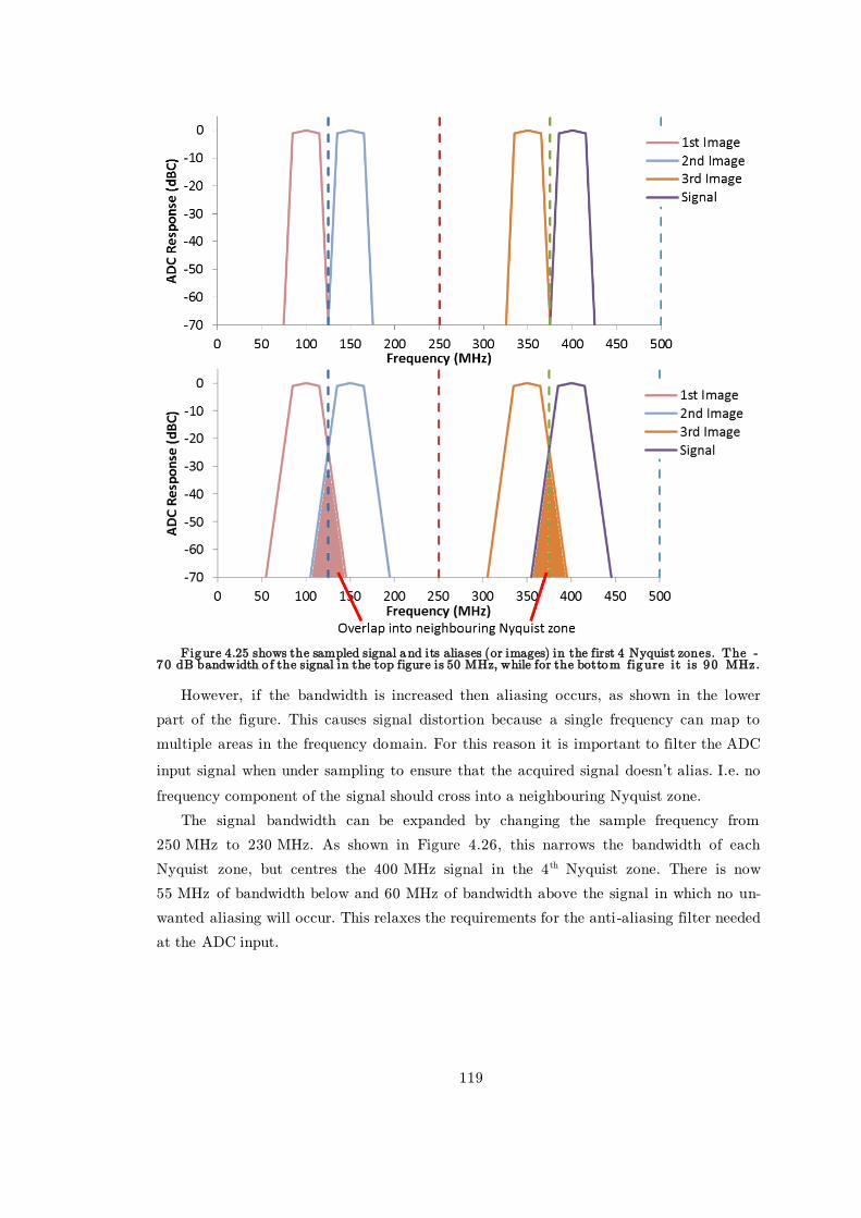
119
Figure 4.25 shows the sampled signal and its aliases (or images) in the first 4 Nyquist zones. The -70 dB bandwidth o f the signal in the top figure is 50 MHz, while for the bottom figure it is 90 MHz.
However, if the bandwidth is increased then aliasing occurs, as shown in the lower
part of the figure. This causes signal distortion because a single frequency can map to
multiple areas in the frequency domain. For this reason it is important to filter the ADC
input signal when under sampling to ensure that the acquired signal doesn’t alias. I.e. no
frequency component of the signal should cross into a neighbouring Nyquist zone.
The signal bandwidth can be expanded by changing the sample frequency from
250 MHz to 230 MHz. As shown in Figure 4.26, this narrows the bandwidth of each
Nyquist zone, but centres the 400 MHz signal in the 4th Nyquist zone. There is now
55 MHz of bandwidth below and 60 MHz of bandwidth above the signal in which no un-
wanted aliasing will occur. This relaxes the requirements for the anti-aliasing filter needed
at the ADC input.
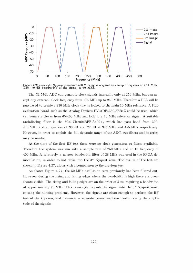
120
Figure 4.26 shows the Nyquist zones for a 400 MHz signal acquired at a sample frequency of 230 MHz. The -70 dB bandwidth o f the signa l is 90 MHz.
The NI 5761 ADC can generate clock signals internally only at 250 MHz, but can ac-
cept any external clock frequency from 175 MHz up to 250 MHz. Therefore a PLL will be
purchased to create a 230 MHz clock that is locked to the main 10 MHz reference. A PLL
evaluation board such as the Analog Devices EV-ADF4360-8EB1Z could be used, which
can generate clocks from 65-400 MHz and lock to a 10 MHz reference signal. A suitable
antialiasing filter is the Mini-CircuitsBPF-A400+, which has pass band from 390-
410 MHz and a rejection of 30 dB and 22 dB at 345 MHz and 455 MHz respectively.
However, in order to exploit the full dynamic range of the ADC, two filters used in series
may be needed.
At the time of the first RF test there were no clock generators or filters available.
Therefore the system was run with a sample rate of 250 MHz and an IF frequency of
400 MHz. A relatively a narrow bandwidth filter of 28 MHz was used in the FPGA de-
modulation, in order to not cross into the 3 rd Nyquist zone. The results of the test are
shown in Figure 4.27, along with a comparison to the previous test.
As shown Figure 4.27, the 50 MHz oscillation seen previously has been filtered out.
However, during the rising and falling edges where the bandwidth is high there are over-
shoots visible. The rising and falling edges are on the order of 5 ns, requiring a bandwidth
of approximately 70 MHz. This is enough to push the signal into the 3 rd Nyquist zone,
causing the aliasing problems. However, the signals are clean enough to perform the RF
test of the klystron, and moreover a separate power head was used to verify the ampl i-
tude of the signals.
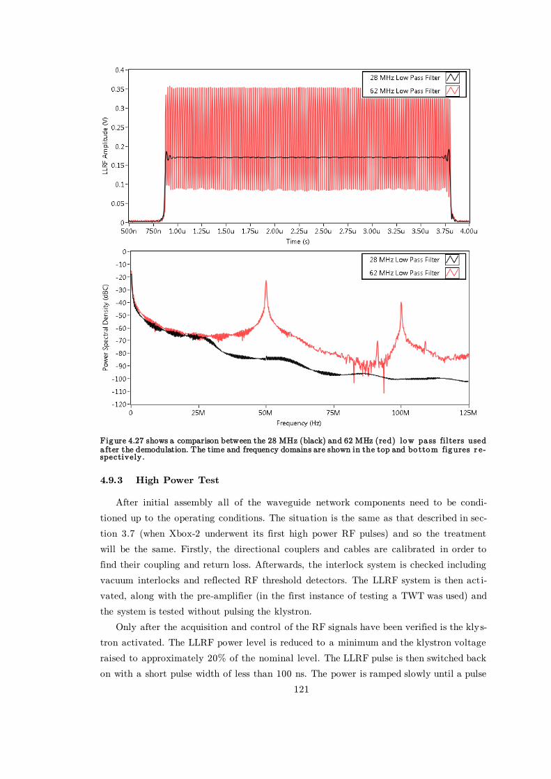
121
Figure 4.27 shows a comparison between the 28 MHz (black) and 62 MHz (red) low pa ss filters used a fter the demodulation. The time and frequency domains are shown in the top and bo ttom figures r e-spectively .
4.9.3 High Power Test
After initial assembly all of the waveguide network components need to be condi-
tioned up to the operating conditions. The situation is the same as that described in sec-
tion 3.7 (when Xbox-2 underwent its first high power RF pulses) and so the treatment
will be the same. Firstly, the directional couplers and cables are calibrated in order to
find their coupling and return loss. Afterwards, the interlock system is checked including
vacuum interlocks and reflected RF threshold detectors. The LLRF system is then acti-
vated, along with the pre-amplifier (in the first instance of testing a TWT was used) and
the system is tested without pulsing the klystron.
Only after the acquisition and control of the RF signals have been verified is the klys-
tron activated. The LLRF power level is reduced to a minimum and the klystron voltage
raised to approximately 20% of the nominal level. The LLRF pulse is then switched back
on with a short pulse width of less than 100 ns. The power is ramped slowly until a pulse
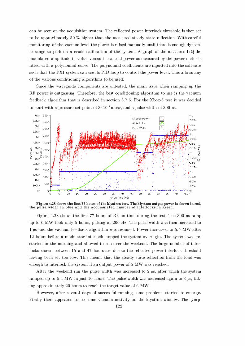
122
can be seen on the acquisition system. The reflected power interlock threshold is then set
to be approximately 50 % higher than the measured steady state reflection. With careful
monitoring of the vacuum level the power is raised manually until there is enough dynam-
ic range to perform a crude calibration of the system. A graph of the measures I/Q de-
modulated amplitude in volts, versus the actual power as measured by the power meter is
fitted with a polynomial curve. The polynomial coefficients are inputted into the software
such that the PXI system can use its PID loop to control the power level. This allows any
of the various conditioning algorithms to be used.
Since the waveguide components are untested, the main issue when ramping up the
RF power is outgassing. Therefore, the best conditioning algorithm to use is the vacuum
feedback algorithm that is described in section 3.7.5. For the Xbox-3 test it was decided
to start with a pressure set point of 3×10⁻⁸ mbar, and a pulse width of 300 ns.
Figure 4.28 shows the first 77 hours of the klystron test. The klystron output power is shown in red, the pulse width in blue and the a ccumula ted number o f interlo cks in g reen.
Figure 4.28 shows the first 77 hours of RF on time during the test. The 300 ns ramp
up to 6 MW took only 5 hours, pulsing at 200 Hz. The pulse width was then increased to
1 𝜇s and the vacuum feedback algorithm was resumed. Power increased to 5.5 MW after
12 hours before a modulator interlock stopped the system overnight. The system was re-
started in the morning and allowed to run over the weekend. The large number of inter-
locks shown between 15 and 47 hours are due to the reflected power interlock threshold
having been set too low. This meant that the steady state reflection from the load was
enough to interlock the system if an output power of 5 MW was reached.
After the weekend run the pulse width was increased to 2 𝜇s, after which the system
ramped up to 5.4 MW in just 10 hours. The pulse width was increased again to 3 𝜇s, tak-
ing approximately 20 hours to reach the target value of 6 MW.
However, after several days of successful running some problems started to emerge.
Firstly there appeared to be some vacuum activity on the klystron window. The symp-
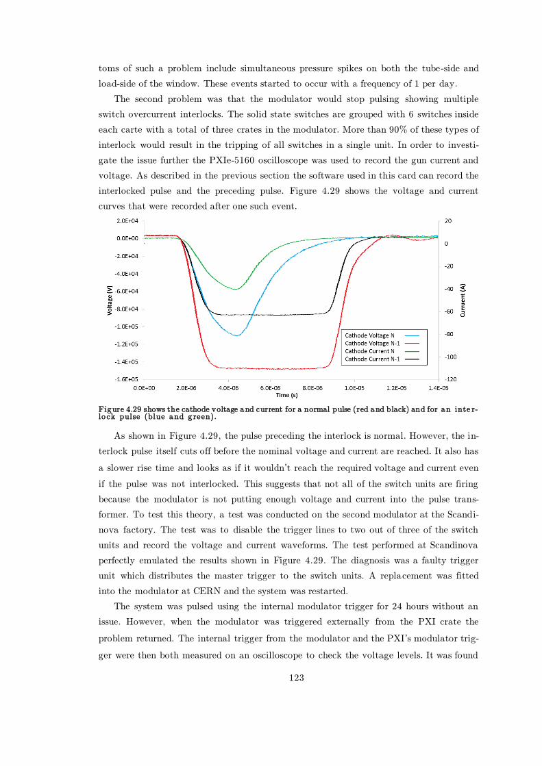
123
toms of such a problem include simultaneous pressure spikes on both the tube-side and
load-side of the window. These events started to occur with a frequency of 1 per day.
The second problem was that the modulator would stop pulsing showing multiple
switch overcurrent interlocks. The solid state switches are grouped with 6 switches inside
each carte with a total of three crates in the modulator. More than 90% of these types of
interlock would result in the tripping of all switches in a single unit. In order to investi-
gate the issue further the PXIe-5160 oscilloscope was used to record the gun current and
voltage. As described in the previous section the software used in this card can record the
interlocked pulse and the preceding pulse. Figure 4.29 shows the voltage and current
curves that were recorded after one such event.
Figure 4.29 shows the cathode voltage and current for a normal pulse (red and black) and for an inte r-lo ck pulse (blue and g reen).
As shown in Figure 4.29, the pulse preceding the interlock is normal. However, the in-
terlock pulse itself cuts off before the nominal voltage and current are reached. It also has
a slower rise time and looks as if it wouldn’t reach the required voltage and current even
if the pulse was not interlocked. This suggests that not all of the switch units are firing
because the modulator is not putting enough voltage and current into the pulse trans-
former. To test this theory, a test was conducted on the second modulator at the Scandi-
nova factory. The test was to disable the trigger lines to two out of three of the switch
units and record the voltage and current waveforms. The test performed at Scandinova
perfectly emulated the results shown in Figure 4.29. The diagnosis was a faulty trigger
unit which distributes the master trigger to the switch units. A replacement was fitted
into the modulator at CERN and the system was restarted.
The system was pulsed using the internal modulator trigger for 24 hours without an
issue. However, when the modulator was triggered externally from the PXI crate the
problem returned. The internal trigger from the modulator and the PXI ’s modulator trig-
ger were then both measured on an oscilloscope to check the voltage levels. It was found

124
that the PXI trigger level was only half as high as the modulator master trigger. At
Xbox-2 this issue didn’t arise because an external interface PCB (as described in section
3.6.3) was used to increase the drive level of the PXI output triggers. The same PCB will
be used in the final Xbox-3 setup, but for the test it was not yet fabricated. A temporary
solution was devised by using an external trigger unit to increase the trigger’s drive level.
A third problem that was encountered during the running of the modulator was that
the phase and amplitude stability would sometimes deteriorate, accompanied by an in-
crease in audible emissions from the modulator. An initial suspicion was that the three
phase supply to the modulator was deteriorating periodically due to loading of the supply
from the PS complex at CERN. A three phase multi-meter was attached to the input of
the modulator to monitor the supply. However, even during the periods where the stabi l-
ity of the modulator was poor the supply to the modulator was clean.
A second line of investigation was opened after speaking with Scandinova. The pulse
transformer has a bias voltage applied to it to reduce the output pulse distortion. Distor-
tion of the output pulse causes the pulse transformer to vibrate more strongly, thus in-
creasing audio emissions. The bias voltage is tuned at the factory by looking at the volt-
age waveform and listening to the noise made by the pulse transformer. The bias voltage
supply was inspected for problems but none were found. However, it was found that there
was a loose connection between the bias supply and the pulse transformer. Once the con-
nection had been secured the distortion issue was solved. It was found that the heater
supply circuit also had a loose connector, which was subsequently secured.
After all of the above issues had been solved the up-time of the experiment was much
improved. This allowed a long run to be conducted with reduced power and pulse width
of the RF to try and condition the klystron window. A new interlock was programmed
into the system to increase the robustness of machine protection against the vacuum
flashover events. Window flashover events are caused by a build-up of plasma near the
window surface [67]. The plasma absorbs some of the RF energy, which appears as a
small cut in power towards the end of the pulse. There is often not much reflected energy
and even if there is, it cannot be measured by the directional coupler because it is placed
after the window. Therefore a method of detecting the missing energy was developed.
After the I/Q demodulation of the klystron output pulse, the amplitude array is inte-
grated in order to calculate the energy of the pulse. The value is stored in a buffer and
then compared with the integrated value from the next pulse. If the ratio between the
new and old pulses is less than 95% then the system is interlocked. In order to stop false
positives the interlock is only activated if the power level is above 250 kW and that the
peak amplitude of the current and previous pulses are within 20% of each other.
The former of the two checks stops false interlocks when there is no RF in the system
and the signals is effectively just noise. The latter check stops a double interlock from
being triggered. For a legitimate missing energy event the peak amplitudes of the inter-
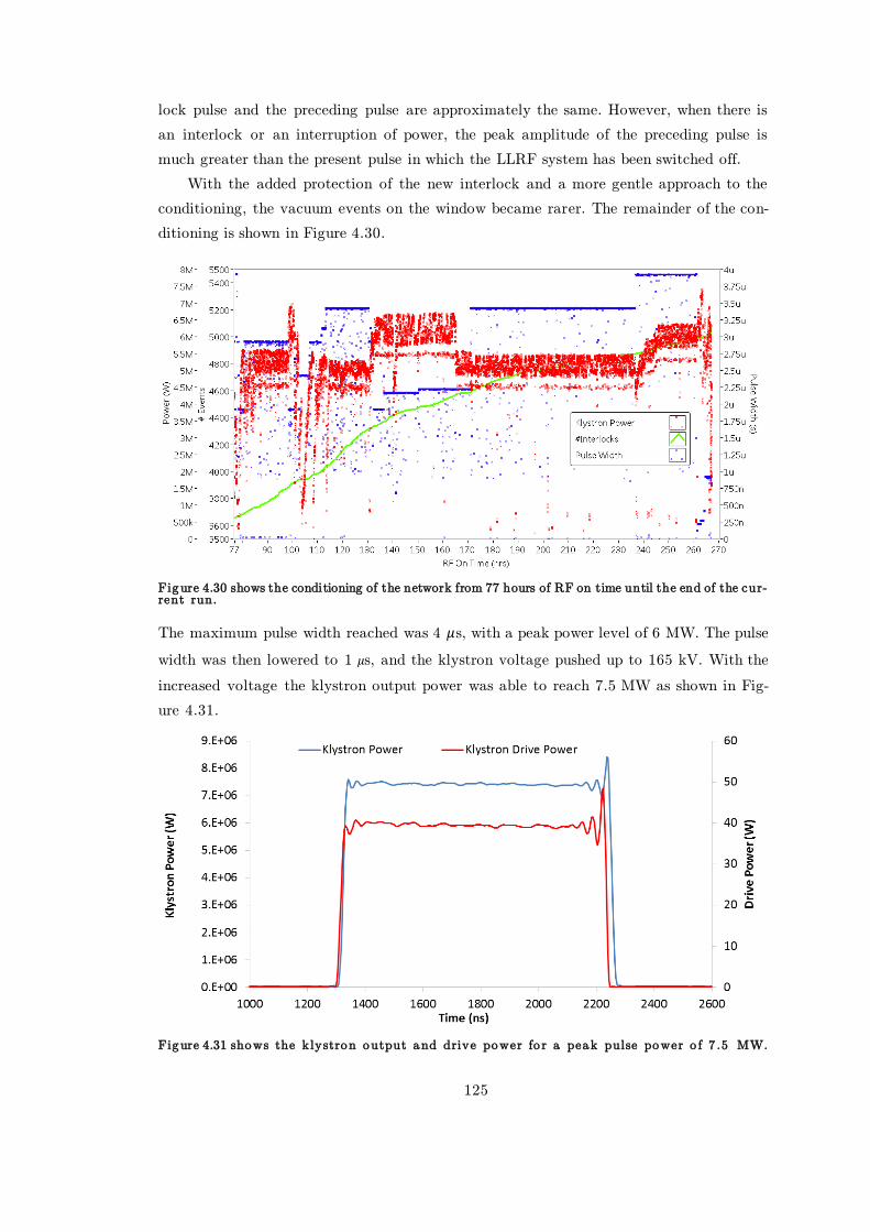
125
lock pulse and the preceding pulse are approximately the same. However, when there is
an interlock or an interruption of power, the peak amplitude of the preceding pulse is
much greater than the present pulse in which the LLRF system has been switched off.
With the added protection of the new interlock and a more gentle approach to the
conditioning, the vacuum events on the window became rarer. The remainder of the con-
ditioning is shown in Figure 4.30.
Figure 4.30 shows the conditioning of the network from 77 hours of RF on time until the end of the cur-rent run.
The maximum pulse width reached was 4 𝜇s, with a peak power level of 6 MW. The pulse
width was then lowered to 1 𝜇s, and the klystron voltage pushed up to 165 kV. With the
increased voltage the klystron output power was able to reach 7.5 MW as shown in Fig-
ure 4.31.
Figure 4.31 shows the klystron output and drive power fo r a peak pulse power o f 7 .5 MW.
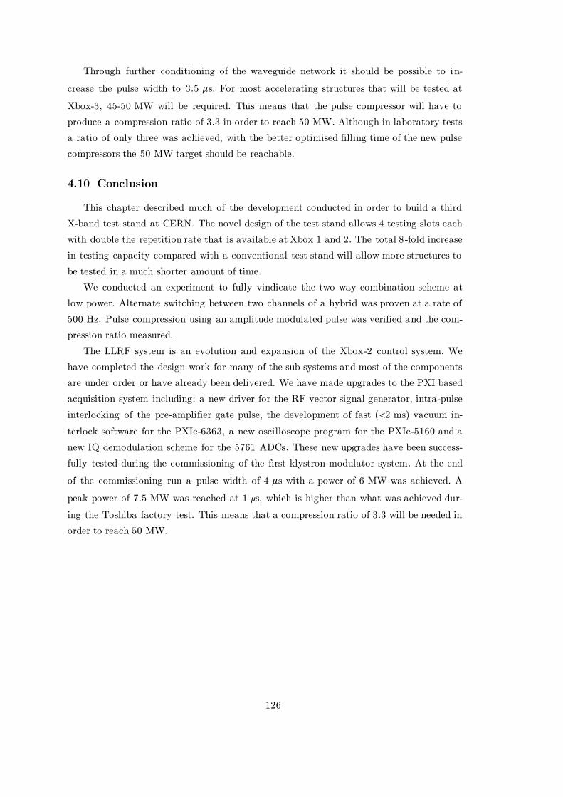
126
Through further conditioning of the waveguide network it should be possible to in-
crease the pulse width to 3.5 𝜇s. For most accelerating structures that will be tested at
Xbox-3, 45-50 MW will be required. This means that the pulse compressor will have to
produce a compression ratio of 3.3 in order to reach 50 MW. Although in laboratory tests
a ratio of only three was achieved, with the better optimised filling time of the new pulse
compressors the 50 MW target should be reachable.
4.10 Conclusion
This chapter described much of the development conducted in order to build a third
X-band test stand at CERN. The novel design of the test stand allows 4 testing slots each
with double the repetition rate that is available at Xbox 1 and 2. The total 8 -fold increase
in testing capacity compared with a conventional test stand will allow more structures to
be tested in a much shorter amount of time.
We conducted an experiment to fully vindicate the two way combination scheme at
low power. Alternate switching between two channels of a hybrid was proven at a rate of
500 Hz. Pulse compression using an amplitude modulated pulse was verified and the com-
pression ratio measured.
The LLRF system is an evolution and expansion of the Xbox-2 control system. We
have completed the design work for many of the sub-systems and most of the components
are under order or have already been delivered. We have made upgrades to the PXI based
acquisition system including: a new driver for the RF vector signal generator, intra-pulse
interlocking of the pre-amplifier gate pulse, the development of fast (<2 ms) vacuum in-
terlock software for the PXIe-6363, a new oscilloscope program for the PXIe-5160 and a
new IQ demodulation scheme for the 5761 ADCs. These new upgrades have been success-
fully tested during the commissioning of the first klystron modulator system. At the end
of the commissioning run a pulse width of 4 𝜇s with a power of 6 MW was achieved. A
peak power of 7.5 MW was reached at 1 𝜇s, which is higher than what was achieved dur-
ing the Toshiba factory test. This means that a compression ratio of 3.3 will be needed in
order to reach 50 MW.

127
Chapter 5
5 The CLIC Crab cavity
As discussed in Chapter 1, CLIC will require crab cavities in order to align the collid-
ing bunches, and thus produce effective head on collisions. A prototype CLIC crab cavity
was developed at Lancaster University. The design considerations, tuning and high power
test results will be presented in this chapter.
5.1 Crab Cavity Design
5.1.1 Crab Cavity Requirements
In order to define the interaction point, the beams at CLIC will collide with a crossing
angle ‘𝜃𝑐 ’ of 20 milli-radians. The horizontal ‘𝜎𝑥’, vertical ‘𝜎𝑦’ and longitudinal ‘𝜎𝑧’ dimen-
sions of the beam at the interaction point are 45 nm, 1 nm and 44 𝜇m respectively. The
luminosity reduction factor ‘𝑆’ can be calculated using the following relation [68].
S =1
√1 + (σzθc2σx
⁄ )2
(5.1)
Equation (5.1), yields a result of 0.1, meaning that 90% of the luminosity is lost com-
pared to that of a head on collision. As shown in Figure 1.5, a crab cavity can be used to
rotate the bunches to restore the lost luminosity. The required deflecting voltage ‘ 𝑉 ’
depends on several factors as shown in Equation (5.2) [69].
𝑉 ≅𝜃𝑐𝐸0𝑐
4𝜋𝑓𝑅12
(5.2)
where ‘𝐸0’ is the beam energy in electron volts, ‘𝑓’ is the RF frequency and ‘𝑅12’ is the
ratio between the horizontal displacement of the beam at the at the IP (interaction point)
and the initial deflection angle provided by the cavity. Horizontal deflection is given by
transverse momentum delivered by the cavity divided by longitudinal momentum. For a
cavity placed just before the final focussing doublet the ‘𝑅12’ value is 23.4 m. The frequen-
cy must be an integer multiple of the bunch repetition rate ‘𝑓𝑟𝑒𝑝’ 1.99903 GHz. In order to
match with the rest of the CLIC project infrastructure and to reduce the required voltage
kick, a frequency of 11.9942GHz is preferred. At the full CLIC beam energy of 1.5 TeV,
the required transverse deflecting voltage is 2.55 MV.
Most commonly used crab cavities have a TM-110 like mode, producing a dipole de-
flecting field. The power level needed to produce the required kick depends on several fac-
tors, including the loaded Q factor, coupling match and the beam loading. For a perfect
128
beam, beam loading is zero because the dipole mode has zero longitudinal fields on axis.
However, the crab cavity will be placed in a high 𝛽 region, where the transverse beam
size and thus beam offset errors will be at their maximum. The vertical and horizontal
beam size at the crab cavity position will be approximately 35 microns and 153 microns
respectively. Neglecting ohmic losses, the power extracted from the cavity due to beam
loading ‘𝑃𝑎 ' from a beam with transverse offset ‘𝑎’ and bunch charge ‘𝑞’ is given by [70]:
𝑃𝑎 = 𝑞𝑉
2𝜋𝑓𝑎
𝑐𝑓𝑟𝑒𝑝 (5.3)
Assuming that the maximum beam offsets are approximately 2-3 times the bunch size
the expected beam loading is of the order of two to four hundred kilowatts. The RF pulse
length at CLIC is approximately 200 ns, so there is not enough time to actively correct
for beam loading. However, if the power flow through the structure is of the order of 10-
20 MW, the level of beam loading becomes negligible. The input RF amplitude and phase
errors also affect the crabbing process. The RF power sources and delivery system are the
main source of the phase and amplitude errors.
5.1.2 RF Cell Design
The high power flow needed to satisfy the beam loading requirements can be accom-
plished by using a travelling wave cavity. Travelling wave deflecting cavities have been
used since the 1960s at many accelerator facilities including SLAC, CERN and BNL [71],
[72]. Disc loaded waveguide type structures are the most commonly used, as the manufac-
turing process allows for micron level tolerances to be achieved. Because of this a disc
loaded structure is the primary choice for the crab cavity. The cell dimensions are chosen
by considering the phase advance per cell, shunt impedance of the crabbing mode, group
velocity, wakefields, power requirement, and the three surface quantities as described in
section 1.3 (peak surface electric field, pulsed temperature rise and scaled power density.)
Initial studies simulated a circularly symmetric cell and varying iris radius and thickness
for phase advances of 120ºand 150º. The best compromise was found for an iris thick-
ness of 2 mm and iris radii between 4.7 mm and 5.7 mm. This yielded structures that re-
quire less than 20 MW of RF power and have between 10 and 13 cells. The peak surface
electric fields are kept below 115 MV/m while pulsed surface heating is below 45 K [70].
Through further wakefield simulations performed by Ambattu and Burt et al. [73] it
was found that the main contribution toward unwanted deflections was from the same
order dipole mode (SOM). This comes from the orthogonally polarized dipole mode,
which can be excited by vertical deflections to the beam. The SOM can be actively
damped by the beam by breaking the circular symmetry of the cell. This was achieved by
using a racetrack cell shape. The frequency of the SOM is shifted such that every other
bunch damps the unwanted mode. The shifted frequency must be a factor of (n+0.5) of
the bunch reputation rate where n is any positive integer. A SOM frequency of 13GHz
was chosen to this effect. In the final design, the lower order monopole mode and higher
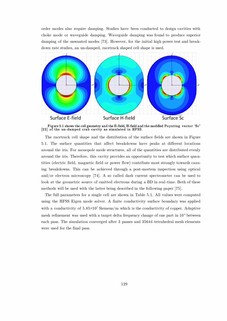
129
order modes also require damping. Studies have been conducted to design cavities with
choke mode or waveguide damping. Waveguide damping was found to produce superior
damping of the unwanted modes [73]. However, for the initial high power test and break-
down rate studies, an un-damped, racetrack shaped cell shape is used.
Figure 5.1 shows the cell geometry and the E-field, H-field and the modified Poynting vecto r ‘Sc ’ [2 2 ] o f the un-damped crab cavity a s simula ted in HFSS.
The racetrack cell shape and the distribution of the surface fields are shown in Figure
5.1. The surface quantities that affect breakdowns have peaks at different locations
around the iris. For monopole mode structures, all of the quantities are distributed evenly
around the iris. Therefore, this cavity provides an opportunity to test which surface quan-
tities (electric field, magnetic field or power flow) contribute most strongly towards caus-
ing breakdowns. This can be achieved through a post-mortem inspection using optical
and/or electron microscopy [74]. A so called dark current spectrometer can be used to
look at the geometric source of emitted electrons during a BD in real -time. Both of these
methods will be used with the latter being described in the following paper [75].
The full parameters for a single cell are shown in Table 5.1. All values were computed
using the HFSS Eigen mode solver. A finite conductivity surface boundary was applied
with a conductivity of 5.85×10⁷ Siemens/m which is the conductivity of copper. Adaptive
mesh refinement was used with a target delta frequency change of one part in 10 4 between
each pass. The simulation converged after 3 passes and 35644 tetrahedral mesh elements
were used for the final pass.

130
Property Value
Frequency 11.9942 GHz
Iris radius 5 mm
Phase advance per cell 120º
Quality Factor 6106
Transverse R/Q 53.8
Kick (normalised to 13.35 MW) 227 kV
Kick per meter 27.2 MV/m
Group Velocity 0.0292c
Attenuation 0.71 Np/m
Peak surface electric field (normalised to 13.35 MW) 89.2 MV/m
Peak surface magnetic (normalised to 13.35 MW) 290 kA/m
Peak modified Poynting vector (normalised to 13.35 MW) 1.71 MW/mm2
Peak pulse surface heating (13.35 MW, 242 ns pulse width) 18ºC
Table 5 .1 Shows the RF properties o f the ra cetra ck crab cavity.
5.1.3 Structure Design
In order to produce the required 2.55 MV kick, 12 cells are needed if a constant im-
pedance structure is used. Constant impedance structures are simpler and cheaper to
manufacture compared with constant gradient structures. Constant gradient structures
require tapering of the cell geometry to maintain the gradient as the power is dissipated
into the copper walls. For a 12 cell structure, the power dissipation is small (on the order
of 15%), meaning that a constant impedance structure can be used.
There are two main types of coupler that can be used to feed power into the struc-
ture. The first is a standard coupler, which couples magnetically to a standard cell. The
second is a waveguide type coupler which couples electrically to a matching cell [76]. Ad-
vantages of the standard coupler include a smaller longitudinal size, lower wakefield con-
tributions and the option to have a single feed structure. The waveguide coupler has a
smaller transverse size, is easier to tune and has lower manufacturing tolerances. If a dual
feed coupler is used, an E-plane splitter is needed to produce two inputs that are in anti-
phase in order to stimulate the dipole mode.

131
Figure 5.2 shows 3D models of a 5 cell crab cavity with the standard coupler (left) and the waveguide coupler (right) [33 ].
Figure 5.2 shows the difference between the two power couplers. Both cavities have 5
active deflecting cells, but the waveguide coupler requires four further cells for mode con-
version and matching. However, the standard coupler requires more transverse space for
several reasons. The waveguide must be tapered to the cell dimensions and space must be
provided between the coupling cell and splitter for the damping waveguides and tuning
pin access. Many of these problems can be avoided by using a single feed coupler. This
eliminates the need for an external splitter and simplifies the manufacturing process.
A single feed geometry breaks the 2-fold symmetry of the design, and as such will in-
troduce monopole and quadrupole components to the field. However, for initial high pow-
er testing and breakdown studies where there is no beam present, the unwanted field
components will not affect the performance. A HFSS simulation was carried out to vali-
date the simulation performed at Lancaster University in 2011 [33] and to facilitate the
tuning of the structure as described in section 5.3. The simulation performed at Lancaster
University used CST Microwave Studio [77], so this simulation provides a benchmark be-
tween the two different codes.
A driven modal simulation was performed with the excitation provided via two wave
ports at the input and output waveguides. The same finite conductivity surface boundary
condition used to simulate the single cell was applied to emulate the conductivity of a
copper surface. In order to reduce the memory load and the volume that needed to be
simulated, the structure was split in half along the YZ plane and a ‘perfect H’ symmetry
boundary used to preserve the fields. For the simulation mesh refinement was used and
the simulation was deemed to be converged after the variation in the S-parameters be-
tween each pass was less than 3 parts in 104. The simulation converged after 8 passes
which took two hours and thirty minutes to run. 871,715 tetrahedrals were used in the
final mesh. The mesh was split into two sections each with a different mesh density. Most
of the structure was simulated with the only constraint being that each mesh element
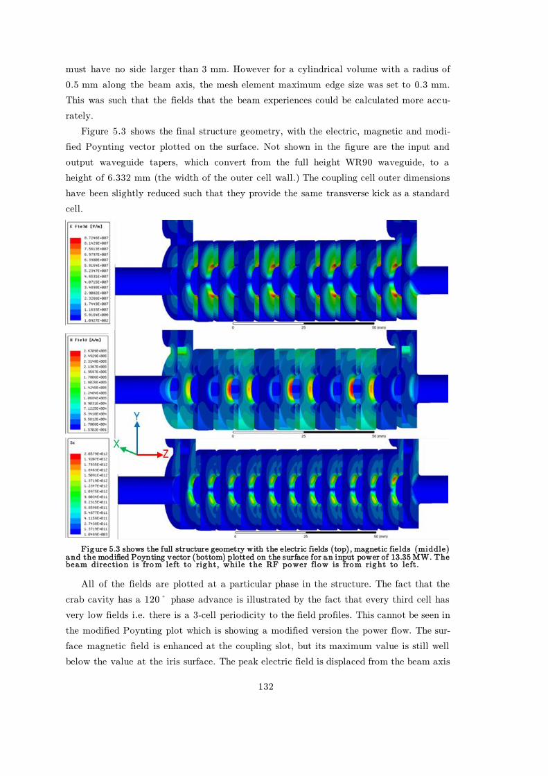
132
must have no side larger than 3 mm. However for a cylindrical volume with a radius of
0.5 mm along the beam axis, the mesh element maximum edge size was set to 0.3 mm.
This was such that the fields that the beam experiences could be calculated more accu-
rately.
Figure 5.3 shows the final structure geometry, with the electric, magnetic and modi-
fied Poynting vector plotted on the surface. Not shown in the figure are the input and
output waveguide tapers, which convert from the full height WR90 waveguide, to a
height of 6.332 mm (the width of the outer cell wall.) The coupling cell outer dimensions
have been slightly reduced such that they provide the same transverse kick as a standard
cell.
Figure 5.3 shows the full structure geometry with the electric fields (top), magnetic fie lds (middle) and the modified Poynting vector (bottom) plotted on the surface for an input power of 13.35 MW. The beam direction is fro m left to right, while the RF power flow is from right to left.
All of the fields are plotted at a particular phase in the structure. The fact that the
crab cavity has a 120º phase advance is illustrated by the fact that every third cell has
very low fields i.e. there is a 3-cell periodicity to the field profiles. This cannot be seen in
the modified Poynting plot which is showing a modified version the power flow. The sur-
face magnetic field is enhanced at the coupling slot, but its maximum value is still well
below the value at the iris surface. The peak electric field is displaced from the beam axis
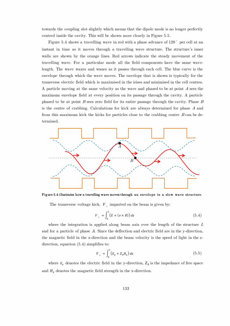
133
towards the coupling slot slightly which means that the dipole mode is no longer perfectly
centred inside the cavity. This will be shown more clearly in Figure 5.5.
Figure 5.4 shows a travelling wave in red with a phase advance of 120º per cell at an
instant in time as it moves through a travelling wave structure. The structure ’s inner
walls are shown by the orange lines. Red arrows indicate the steady movement of the
travelling wave. For a particular mode all the field components have the same wave-
length. The wave waxes and wanes as it passes through each cell. The blue curve is the
envelope through which the wave moves. The envelope that is shown is typically for the
transverse electric field which is maximised in the irises and minimised in the cell centres.
A particle moving at the same velocity as the wave and phased to be at point A sees the
maximum envelope field at every position on its passage through the cavity. A particle
phased to be at point B sees zero field for its entire passage through the cavity. Phase B
is the centre of crabbing. Calculations for kick are always determined for phase A and
from this maximum kick the kicks for particles close to the crabbing centre B can be de-
termined.
Figure 5.4 illustrates how a travelling wave moves through an envelope in a slow wave structure.
The transverse voltage kick, 𝑉 imparted on the beam is given by:
𝑉 = ∫ (𝐸 + (𝑣 × 𝐵))𝐿
0𝑑𝑧 (5.4)
where the integration is applied along beam axis over the length of the structure L
and for a particle of phase A. Since the deflection and electric field are in the y-direction,
the magnetic field in the x-direction and the beam velocity is the speed of light in the z-
direction, equation (5.4) simplifies to:
𝑉 = ∫ (𝐸𝑦 + 𝑍0𝐻𝑥)𝐿
0𝑑𝑧 (5.5)
where 𝐸𝑦 denotes the electric field in the y-direction, 𝑍0 is the impedance of free space
and 𝐻𝑥 denotes the magnetic field strength in the x-direction.
A
B
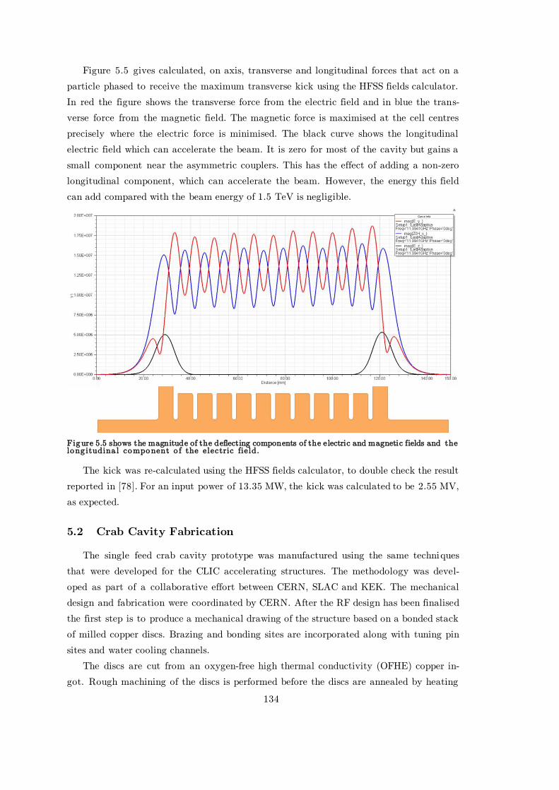
134
Figure 5.5 gives calculated, on axis, transverse and longitudinal forces that act on a
particle phased to receive the maximum transverse kick using the HFSS fields calculator.
In red the figure shows the transverse force from the electric field and in blue the trans-
verse force from the magnetic field. The magnetic force is maximised at the cell centres
precisely where the electric force is minimised. The black curve shows the longitudinal
electric field which can accelerate the beam. It is zero for most of the cavity but gains a
small component near the asymmetric couplers. This has the effect of adding a non-zero
longitudinal component, which can accelerate the beam. However, the energy this field
can add compared with the beam energy of 1.5 TeV is negligible.
Figure 5.5 shows the magnitude of the deflecting components of the electric and magnetic fields and the long itudina l component o f the electric fie ld.
The kick was re-calculated using the HFSS fields calculator, to double check the result
reported in [78]. For an input power of 13.35 MW, the kick was calculated to be 2.55 MV,
as expected.
5.2 Crab Cavity Fabrication
The single feed crab cavity prototype was manufactured using the same techniques
that were developed for the CLIC accelerating structures. The methodology was devel-
oped as part of a collaborative effort between CERN, SLAC and KEK. The mechanical
design and fabrication were coordinated by CERN. After the RF design has been finalised
the first step is to produce a mechanical drawing of the structure based on a bonded stack
of milled copper discs. Brazing and bonding sites are incorporated along with tuning pin
sites and water cooling channels.
The discs are cut from an oxygen-free high thermal conductivity (OFHE) copper in-
got. Rough machining of the discs is performed before the discs are annealed by heating
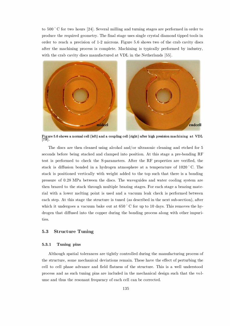
135
to 500ºC for two hours [24]. Several milling and turning stages are performed in order to
produce the required geometry. The final stage uses single crystal diamond tipped tools in
order to reach a precision of 1-2 microns. Figure 5.6 shows two of the crab cavity discs
after the machining process is complete. Machining is typically performed by industry,
with the crab cavity discs manufactured at VDL in the Netherlands [55].
Figure 5.6 shows a normal cell (left) and a coupling cell (right) after high presision machining a t VDL [79 ].
The discs are then cleaned using alcohol and/or ultrasonic cleaning and etched for 5
seconds before being stacked and clamped into position. At this stage a pre-bonding RF
test is performed to check the S-parameters. After the RF properties are verified, the
stack is diffusion bonded in a hydrogen atmosphere at a temperature of 1020ºC. The
stack is positioned vertically with weight added to the top such that there is a bonding
pressure of 0.28 MPa between the discs. The waveguides and water cooling system are
then brazed to the stack through multiple brazing stages. For each stage a brazing mate-
rial with a lower melting point is used and a vacuum leak check is performed between
each step. At this stage the structure is tuned (as described in the next sub-section), after
which it undergoes a vacuum bake out at 650ºC for up to 10 days. This removes the hy-
drogen that diffused into the copper during the bonding process along with other impuri-
ties.
5.3 Structure Tuning
5.3.1 Tuning pins
Although spatial tolerances are tightly controlled during the manufacturing process of
the structure, some mechanical deviations remain. These have the effect of perturbing the
cell to cell phase advance and field flatness of the structure. This is a well understood
process and as such tuning pins are included in the mechanical design such that the vo l-
ume and thus the resonant frequency of each cell can be corrected.
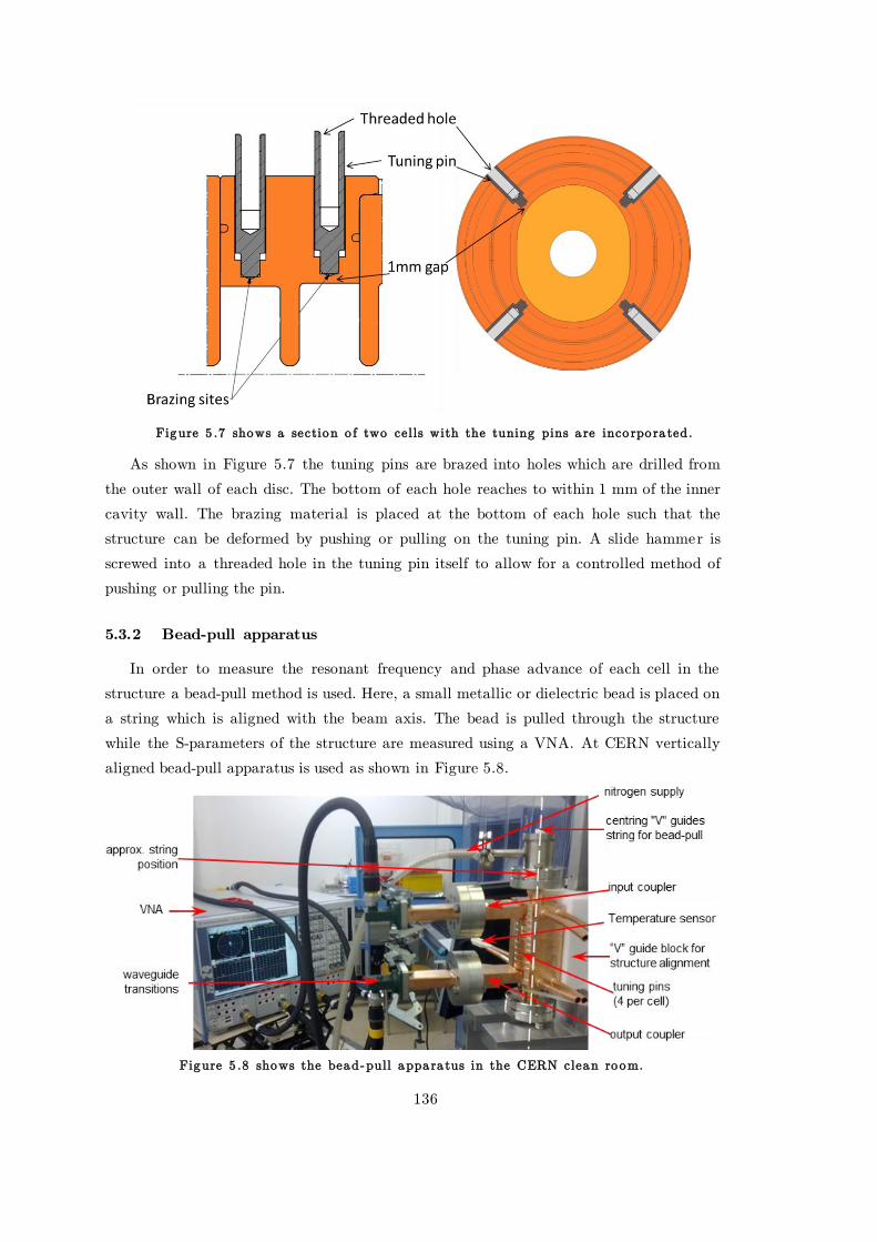
136
Figure 5 .7 shows a section o f two cells with the tuning pins a re inco rpo ra ted.
As shown in Figure 5.7 the tuning pins are brazed into holes which are drilled from
the outer wall of each disc. The bottom of each hole reaches to within 1 mm of the inner
cavity wall. The brazing material is placed at the bottom of each hole such that the
structure can be deformed by pushing or pulling on the tuning pin. A slide hammer is
screwed into a threaded hole in the tuning pin itself to allow for a controlled method of
pushing or pulling the pin.
5.3.2 Bead-pull apparatus
In order to measure the resonant frequency and phase advance of each cell in the
structure a bead-pull method is used. Here, a small metallic or dielectric bead is placed on
a string which is aligned with the beam axis. The bead is pulled through the structure
while the S-parameters of the structure are measured using a VNA. At CERN vertically
aligned bead-pull apparatus is used as shown in Figure 5.8.
Figure 5 .8 shows the bead-pull appara tus in the CERN clean room.

137
The temperature of the structure is monitored and dry nitrogen is pumped through
such that the moisture in the air doesn’t introduce unknown contributions to the electric
permittivity inside the structure. With the temperature and permittivity known the fre-
quency at which the measurement is taken can be calculated from the operating point of
11.9942 GHz in vacuum at 30ºC. The nylon string that is used to hold the bead also
causes a frequency perturbation. To correct for this effect, the S-parameters of the struc-
ture are measured with and then without the string in place.
5.3.3 Bead choice and field perturbations
When a travelling wave as illustrated in Figure 5.4 moves through a structure there is
no reflection when the cavity is perfectly tuned and the phase advance in each cell is ex-
actly 120º. If a bead is placed at some point in the structure it gives rise to an imped-
ance miss-match and reflects part of the wave from its location. Reflection caused by the
perturbing effect of the bead is proportional to the weighted sum of all of the electromag-
netic field components squared at the location of the bead [80]:
∆𝑺𝟏𝟏~ ∑ {(𝒆∗𝑬∗)𝟐 − (𝒁𝑭𝟎𝒉∗𝑯∗)
𝟐}
∗=𝒙,𝒚,𝒛
(5.6)
Where ∆𝑺𝟏𝟏 is the change in reflection associated with the bead. The complex compo-
nents ex, ey, ez, hx, hy and hz describe the polarisation and magnetisation effects of the
bead in the local electromagnetic field.
When choosing a bead type (metallic or dielectric) it is important to consider which
field component will give the best measurement. A metallic bead perturbs both the mag-
netic and electric field components, while a dielectric bead perturbs only the electric field
[81]. For accelerating structures it is usually sufficient to measure and correct only one
component of the field. However, in the crab cavity the beam is deflected by both electric
and magnetic fields. It is possible to measure with a metallic and conductive bead and use
calculation to separate the magnetic and electric field components [81].
However, in order to reduce the number of measurements needed and the time in
which the structure is exposed to air, it is preferable to use only one type of bead. Alt-
hough the deflection is affected by both the magnetic and electric field components, simu-
lations conducted in the previous sub-section show that the relationship between the elec-
tric and magnetic field is well understood (Figure 5.5).
To a first approximation the transverse variation of fields along the cavity beam axis
can be shown to be:
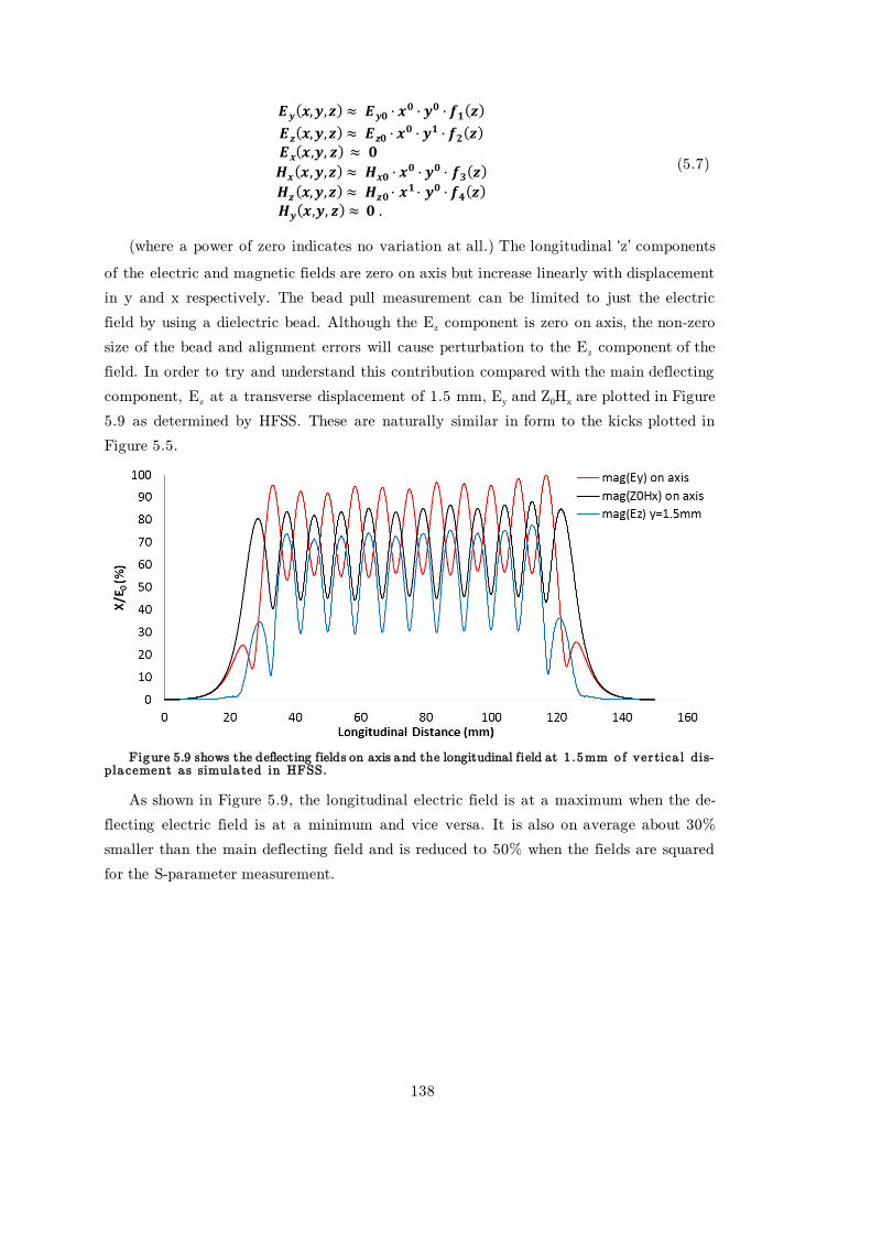
138
𝑬𝒚(𝒙,𝒚,𝒛) ≈ 𝑬𝒚𝟎 · 𝒙𝟎 · 𝒚𝟎 · 𝒇𝟏(𝒛)
𝑬𝒛(𝒙,𝒚,𝒛) ≈ 𝑬𝒛𝟎 · 𝒙𝟎 · 𝒚𝟏 · 𝒇𝟐(𝒛)
𝑬𝒙(𝒙,𝒚, 𝒛) ≈ 𝟎
𝑯𝒙(𝒙,𝒚,𝒛) ≈ 𝑯𝒙𝟎 · 𝒙𝟎 · 𝒚𝟎 · 𝒇𝟑(𝒛)
𝑯𝒛(𝒙,𝒚,𝒛) ≈ 𝑯𝒛𝟎 · 𝒙𝟏 · 𝒚𝟎 · 𝒇𝟒(𝒛)
𝑯𝒚(𝒙,𝒚, 𝒛) ≈ 𝟎 .
(5.7)
(where a power of zero indicates no variation at all.) The longitudinal ‘z’ components
of the electric and magnetic fields are zero on axis but increase linearly with displacement
in y and x respectively. The bead pull measurement can be limited to just the electric
field by using a dielectric bead. Although the Ez component is zero on axis, the non-zero
size of the bead and alignment errors will cause perturbation to the Ez component of the
field. In order to try and understand this contribution compared with the main deflecting
component, Ez at a transverse displacement of 1.5 mm, Ey and Z0Hx are plotted in Figure
5.9 as determined by HFSS. These are naturally similar in form to the kicks plotted in
Figure 5.5.
Figure 5.9 shows the deflecting fields on axis and the longitudinal field at 1 .5mm o f vertica l dis-pla cement a s simula ted in HFSS.
As shown in Figure 5.9, the longitudinal electric field is at a maximum when the de-
flecting electric field is at a minimum and vice versa. It is also on average about 30%
smaller than the main deflecting field and is reduced to 50% when the fields are squared
for the S-parameter measurement.

139
Figure 5.10 shows the ∆𝑺𝟏𝟏 for a bead on axis and vertically offset by 0.8 mm and 1 .2 mm [82 ]. The simula ted leng th co rresponds to 2 .5 no rma l cells.
Simulations of the bead motion were conducted for different lateral bead displace-
ments. Figure 5.10 shows how the ∆𝑆11 changes at the various displacements and that a
relatively high offset of 0.8 mm still produces a usable profile. The third graph in Figure
5.10 shows the real and imaginary parts of the reflected signal as the bead is progressively
moved along the cavity. The wave travels from the input coupler to the bead with mini-
mal reflection. The bead then causes a fractional reflection of the power, which returns to
the input coupler in an identical mode. The phase of the reflected signal gives the location
of the bead. The amplitude of the reflected signal is proportional to that of the unper-
turbed field. As the amplitude varies between the iris and the cell centre the phase ad-
vance per cell is clearly observed. When every cell has a precise phase advance of 120º,
reflection from the bead for each cell overlays that from the previous cell exactly. For
transverse displacements larger than 0.8 mm the amplitude passes through zero and then
the phase advance per cell switches to become positive making interpretation of the re-
sults difficult. When performing the measurement the correct alignment of the bead can
be verified by monitoring the cell to cell phase advance.
5.3.4 Bead-pull Method and Results
In order to make the measurement, the bead was moved from the output to the input
of the structure, while measuring S11 at the input. An initial measurement was carried
out to check that the bead perturbed the fields as expected and to verify the experimental
apparatus. The results are shown in Figure 5.11. At the start of the bead pull (i.e. in the
output cells), the plots behave as expected, with a 3 leaf pattern and a negatively advanc-
ing phase. However, between cells 8 and 9 it becomes positive. The leaf pattern also de-
generates into a more triangular shape. In the previous sub-section, Figure 5.10 shows
how transverse deflection of the bead can distort the plot in the complex plane and cause
a sign change in the phase advance.
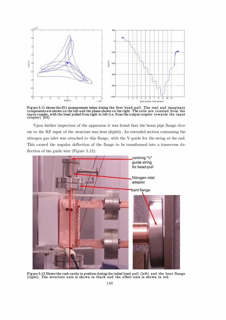
140
Figure 5.11 shows the S11 measurement taken during the first bead-pull. The rea l and imag ina ry components a re shown on the left and the phase shown on the right. The cells a re counted from the input coupler, with the bead pulled from right to left (i.e. from the output coupler towards the input coupler) [83 ].
Upon further inspection of the apparatus it was found that the beam pipe flange clo s-
est to the RF input of the structure was bent slightly. An extended section containing the
nitrogen gas inlet was attached to this flange, with the V-guide for the string at the end.
This caused the angular deflection of the flange to be transformed into a transverse de-
flection of the guide wire (Figure 5.12).
Figure 5.12 Shows the crab cavity in position during the initial bead pull (left) and the bent flange (right). The structure axis is shown in bla ck and the o ffset axis is shown in red.
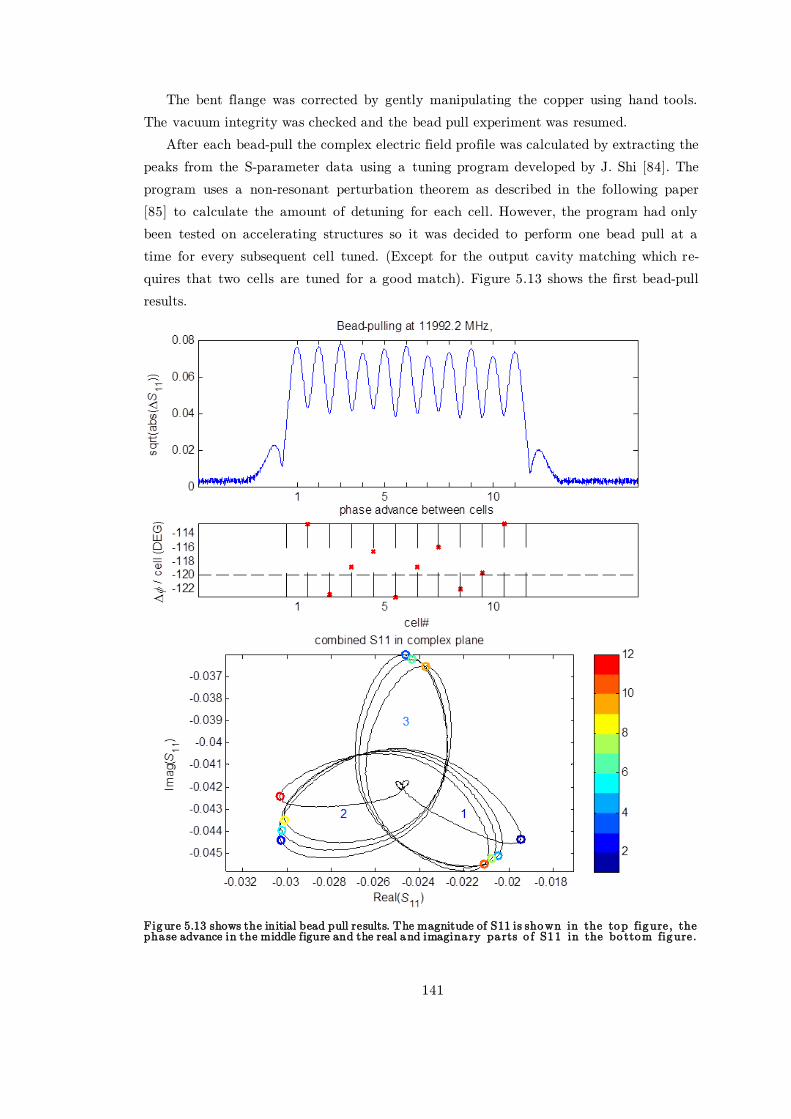
141
The bent flange was corrected by gently manipulating the copper using hand tools.
The vacuum integrity was checked and the bead pull experiment was resumed.
After each bead-pull the complex electric field profile was calculated by extracting the
peaks from the S-parameter data using a tuning program developed by J. Shi [84]. The
program uses a non-resonant perturbation theorem as described in the following paper
[85] to calculate the amount of detuning for each cell. However, the program had only
been tested on accelerating structures so it was decided to perform one bead pull at a
time for every subsequent cell tuned. (Except for the output cavity matching which re-
quires that two cells are tuned for a good match). Figure 5.13 shows the first bead-pull
results.
Figure 5.13 shows the initial bead pull results. The magnitude of S11 is shown in the top figure, the phase advance in the middle figure and the real and imagina ry pa rts o f S11 in the bo ttom figure.
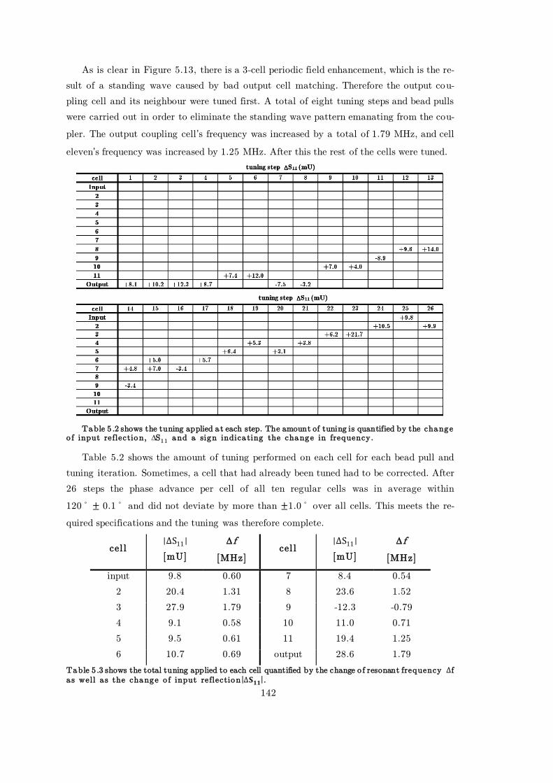
142
As is clear in Figure 5.13, there is a 3-cell periodic field enhancement, which is the re-
sult of a standing wave caused by bad output cell matching. Therefore the output cou-
pling cell and its neighbour were tuned first. A total of eight tuning steps and bead pulls
were carried out in order to eliminate the standing wave pattern emanating from the cou-
pler. The output coupling cell’s frequency was increased by a total of 1.79 MHz, and cell
eleven’s frequency was increased by 1.25 MHz. After this the rest of the cells were tuned.
Table 5 .2 shows the tuning applied a t each step. The amount of tuning is quantified by the change o f input reflection, ∆S1 1 and a sign indica ting the change in frequency.
Table 5.2 shows the amount of tuning performed on each cell for each bead pull and
tuning iteration. Sometimes, a cell that had already been tuned had to be corrected. After
26 steps the phase advance per cell of all ten regular cells was in average within
120º ± 0.1º and did not deviate by more than ±1.0º over all cells. This meets the re-
quired specifications and the tuning was therefore complete.
cel l |∆S11 |
[mU]
f
[MHz] cel l
|∆S11|
[mU]
f
[MHz]
input 9.8 0.60 7 8.4 0.54
2 20.4 1.31 8 23.6 1.52
3 27.9 1.79 9 -12.3 -0.79
4 9.1 0.58 10 11.0 0.71
5 9.5 0.61 11 19.4 1.25
6 10.7 0.69 output 28.6 1.79
Table 5 .3 shows the total tuning applied to each cell quantified by the change o f resonant frequency ∆f
a s well a s the change o f input reflection |∆𝐒𝟏𝟏|.
143
An overall summary of the tuning per cell is shown in Table 5.3. The final bead-pull
measurement results are shown in Figure 5.14. For the most part, the structure had been
made too large, with all cells except cell 9 requiring an increase in frequency. The average
tuning performed across these cells was 0.8 MHz per cell. A measured standard deviation
of 0.7 MHz, relates to a spread of 1 micron in the cell's diameter, underlining the excel-
lent machining and assembly quality.
Figure 5.14 shows the bead pull results for the fully tuned CLIC crab cavity. The magnitude o f S11 is shown in the top figure, the phase advance in the middle figure and the real and imaginary parts of S11 in the bo ttom figure.
Once the tuning had been completed the cavity was baked in a vacuum furnace at
650ºC for a period of ten days to remove impurities introduced during the bonding pro-
cess and subsequent handling during the tuning process.
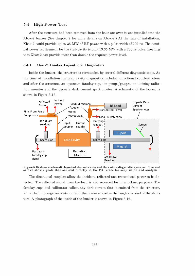
144
5.4 High Power Test
After the structure had been removed from the bake out oven it was insta lled into the
Xbox-2 bunker (See chapter 2 for more details on Xbox-2.) At the time of installation,
Xbox-2 could provide up to 35 MW of RF power with a pulse width of 200 ns. The nomi-
nal power requirement for the crab cavity is only 13.35 MW with a 200 ns pulse, meaning
that Xbox-2 can provide more than double the required power level.
5.4.1 Xbox-2 Bunker Layout and Diagnostics
Inside the bunker, the structure is surrounded by several different diagnostic tools. At
the time of installation the crab cavity diagnostics included: directional couplers before
and after the structure, an upstream faraday cup, ion pumps/gauges, an ionizing radia-
tion monitor and the Uppsala dark current spectrometer. A schematic of the layout is
shown in Figure 5.15.
Figure 5.15 shows a schematic layout o f the crab cavity and the various diagno stic systems. The red a rrows show signa ls tha t a re sent directly to the PXI cra te fo r a cquisi tion and ana lysis.
The directional couplers allow the incident, reflected and transmitted power to be de-
tected. The reflected signal from the load is also recorded for interlocking purposes. The
faraday cups and collimator collect any dark current that is emitted from the structure,
while the ion gauge readouts monitor the pressure level in the neighbourhood of the struc-
ture. A photograph of the inside of the bunker is shown in Figure 5.16.
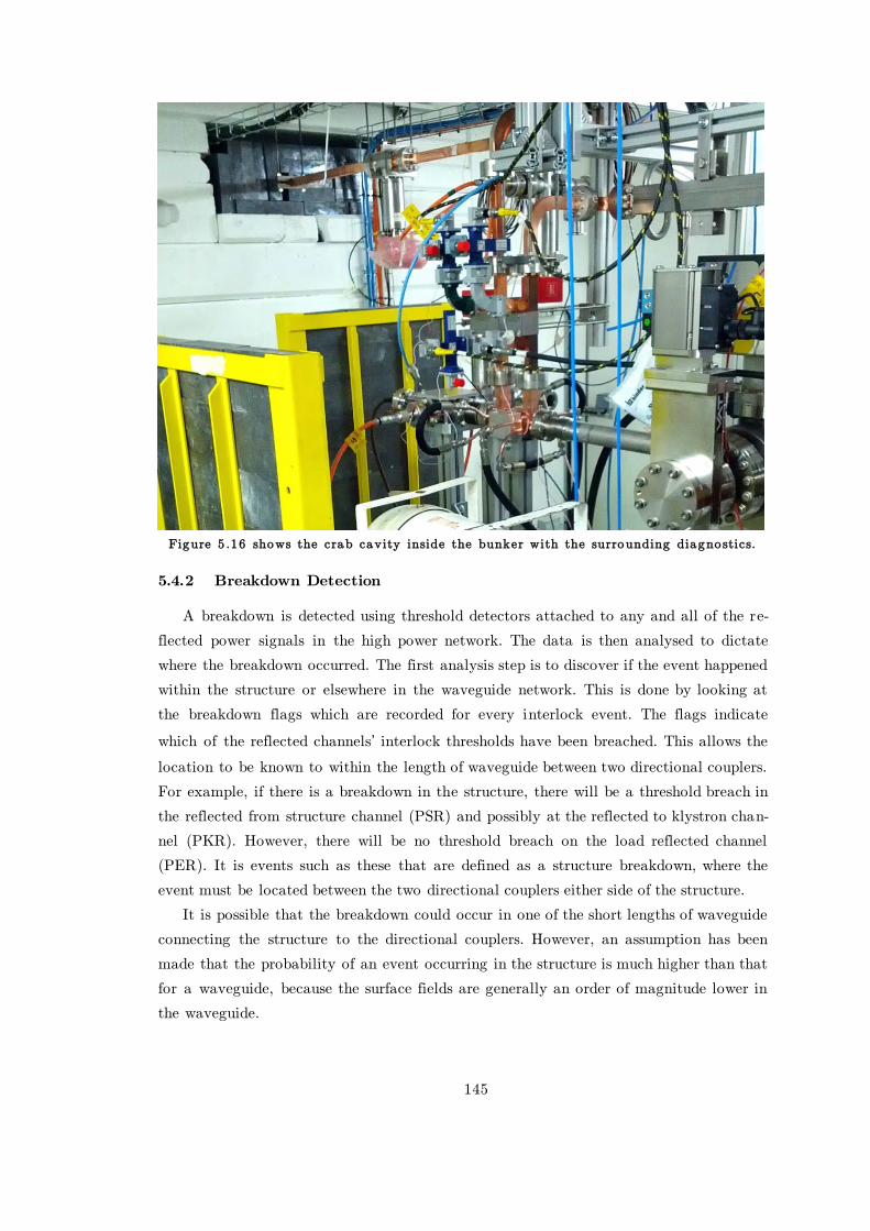
145
Figure 5 .16 shows the crab cavity inside the bunker with the surrounding diagnostics.
5.4.2 Breakdown Detection
A breakdown is detected using threshold detectors attached to any and all of the re-
flected power signals in the high power network. The data is then analysed to dictate
where the breakdown occurred. The first analysis step is to discover if the event happened
within the structure or elsewhere in the waveguide network. This is done by looking at
the breakdown flags which are recorded for every interlock event. The flags indicate
which of the reflected channels’ interlock thresholds have been breached. This allows the
location to be known to within the length of waveguide between two directional couplers.
For example, if there is a breakdown in the structure, there will be a threshold breach in
the reflected from structure channel (PSR) and possibly at the reflected to klystron chan-
nel (PKR). However, there will be no threshold breach on the load reflected channel
(PER). It is events such as these that are defined as a structure breakdown, where the
event must be located between the two directional couplers either side of the structure.
It is possible that the breakdown could occur in one of the short lengths of waveguide
connecting the structure to the directional couplers. However, an assumption has been
made that the probability of an event occurring in the structure is much higher than that
for a waveguide, because the surface fields are generally an order of magnitude lower in
the waveguide.

146
5.4.3 Conditioning Process
The process for the high power test will be the same as that used to test the TD26CC
CLIC accelerating structure [86]. The TD26CC was tested at Xbox-1 using the condition-
ing algorithm that was described in section 2.4.4. The algorithm is used to raise the input
power of the structure in a controlled manner, while maintaining a specific breakdown
rate. Use of the algorithm is important to maintain consistency between all the structures
that have been and will be tested at CERN in the future.
The pulse width is controlled manually and is typically changed by the operator every
few days or weeks depending on the structure being tested. An outline of the whole condi-
tioning process is given in Figure 5.17.
Figure 5.17 shows the generalised conditioning curve used to process high g radient structures a t CERN and KEK. Total conditioning time is usua lly a round 2000 RF hours i.e . 360 million pulses.
As outlined in Figure 5.17, the conditioning process follows a simple procedure: the
pulse width is set by the operator to 50 ns and the power is ramped using the condition-
ing algorithm which maintains a constant BDR. The power is ramped to a few percent
(typically 5-10%) above the target operating level after which the pulse length is in-
creased by 50 ns. The process is repeated until the final operating conditions are met. The
procedure is sometimes changed, for instance if the structure is ramping up in power very
quickly the pulse width may be increased by more than 50 ns at a time.
5.4.4 Conditioning Results
The flat-top pulse width was set to 100 ns in the crab cavity and the power was
ramped manually until the first breakdown event was observed. After this the power was
reduced by 10 % and control was handed over to the conditioning algorithm which was
operated in constant breakdown rate mode. The breakdown rate set point was set to
5×10⁻⁵ breakdowns per pulse (BDs/pulse). An interim target power level of 10 MW was
set and the system was allowed to run. The results are shown in Figure 5.18.
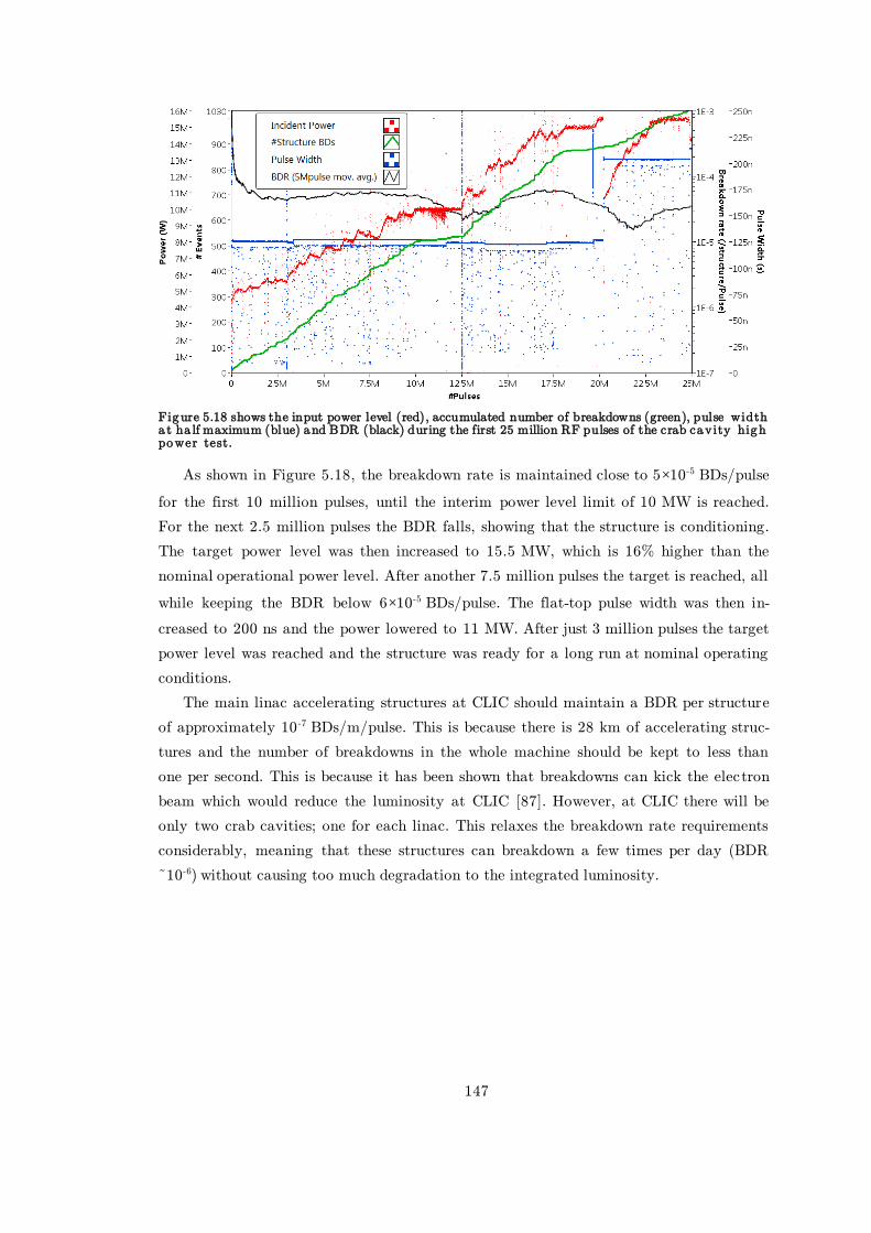
147
Figure 5.18 shows the input power level (red), accumulated number of breakdowns (green), pulse width a t ha lf maximum (blue) and BDR (black) during the first 25 million RF pulses of the crab cavity high power test.
As shown in Figure 5.18, the breakdown rate is maintained close to 5×10⁻⁵ BDs/pulse
for the first 10 million pulses, until the interim power level limit of 10 MW is reached.
For the next 2.5 million pulses the BDR falls, showing that the structure is conditioning.
The target power level was then increased to 15.5 MW, which is 16% higher than the
nominal operational power level. After another 7.5 million pulses the target is reached, all
while keeping the BDR below 6×10⁻⁵ BDs/pulse. The flat-top pulse width was then in-
creased to 200 ns and the power lowered to 11 MW. After just 3 million pulses the target
power level was reached and the structure was ready for a long run at nominal operating
conditions.
The main linac accelerating structures at CLIC should maintain a BDR per structure
of approximately 10 -7 BDs/m/pulse. This is because there is 28 km of accelerating struc-
tures and the number of breakdowns in the whole machine should be kept to less than
one per second. This is because it has been shown that breakdowns can kick the electron
beam which would reduce the luminosity at CLIC [87]. However, at CLIC there will be
only two crab cavities; one for each linac. This relaxes the breakdown rate requirements
considerably, meaning that these structures can breakdown a few times per day (BDR
~10-6) without causing too much degradation to the integrated luminosity.
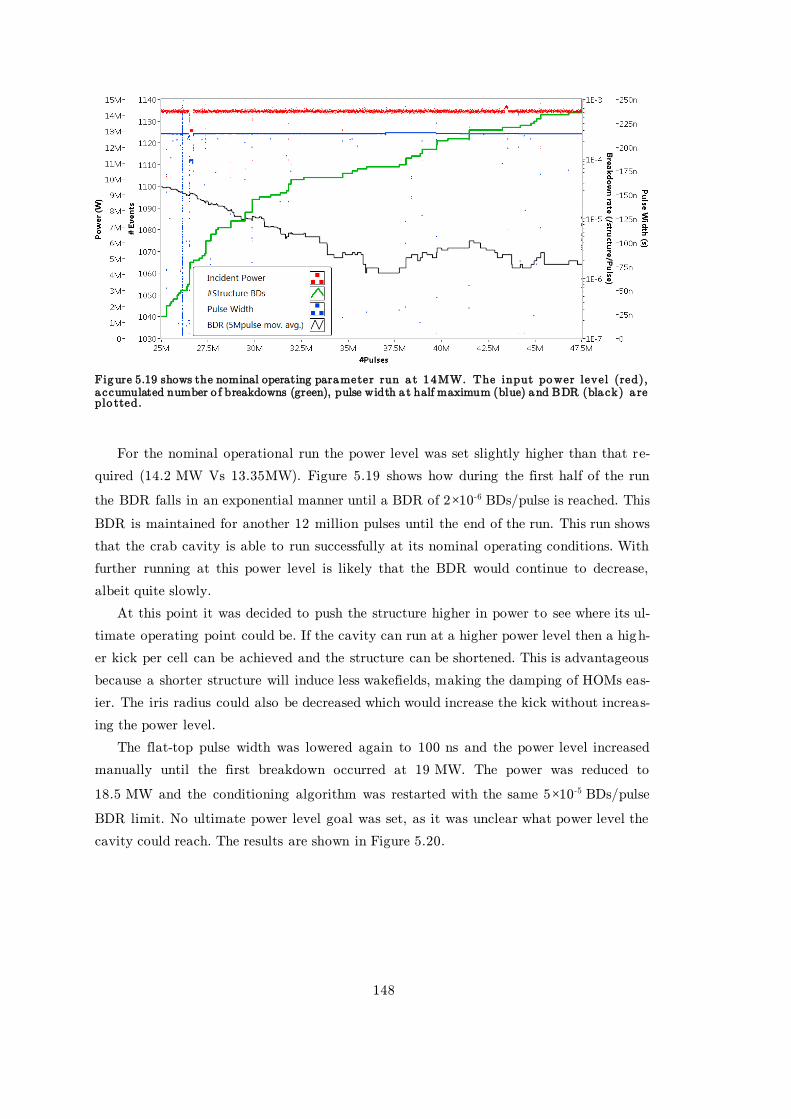
148
Figure 5.19 shows the nominal operating parameter run a t 14MW. The input power level (red), a ccumulated number o f breakdowns (green), pulse width a t half maximum (blue) and BDR (bla ck) a re plo tted.
For the nominal operational run the power level was set slightly higher than that re-
quired (14.2 MW Vs 13.35MW). Figure 5.19 shows how during the first half of the run
the BDR falls in an exponential manner until a BDR of 2×10⁻⁶ BDs/pulse is reached. This
BDR is maintained for another 12 million pulses until the end of the run. This run shows
that the crab cavity is able to run successfully at its nominal operating conditions. With
further running at this power level is likely that the BDR would continue to decrease,
albeit quite slowly.
At this point it was decided to push the structure higher in power to see where its ul-
timate operating point could be. If the cavity can run at a higher power level then a high-
er kick per cell can be achieved and the structure can be shortened. This is advantageous
because a shorter structure will induce less wakefields, making the damping of HOMs eas-
ier. The iris radius could also be decreased which would increase the kick without increas-
ing the power level.
The flat-top pulse width was lowered again to 100 ns and the power level increased
manually until the first breakdown occurred at 19 MW. The power was reduced to
18.5 MW and the conditioning algorithm was restarted with the same 5×10⁻⁵ BDs/pulse
BDR limit. No ultimate power level goal was set, as it was unclear what power level the
cavity could reach. The results are shown in Figure 5.20.

149
Figure 5.20 shows the conditioning curve from 18.5 MW up to 27 MW for a 100 ns flat-top pulse width. The input power level (red), accumulated number of breakdowns (green), pulse width at half maximum (blue) and BDR (bla ck) a re plo tted.
As shown in Figure 5.20, the power ramps up in a stable fashion up until a power lev-
el of 26 MW is reached. At this point there is quite a sharp decrease in power level be-
tween the 60 and 61 million pulse marks. This is due to a cluster of a hundred break-
downs, to which the conditioning algorithm reacted by lowering the power level. At this
point to try and protect the structure from too many breakdowns it was decided to lower
the BDR set point from 5×10⁻⁵ BDs/pulse to 4×10⁻⁵ BDs/pulse. The power level recovered
and reached 27 MW after which a series of breakdown cluster events suggested that a
hard limit had been reached. After 72 million pulses and during a breakdown cluster
event the power level was reduced to 25 MW to see if the structure was stable at this
power level. After a further 6 million pulses the structure was running stably with a BDR
of 1.5×10⁻⁵ BDs/pulse.
It was then decided to increase the flat top pulse width to 200 ns and run at a power
level of 20.3 MW, in order to test the stability of the structure at this new power level.
The integrated kick of the structure at this power level is 3.14 MV, meaning that the
structure length could be reduced by two cells in order to provide the required 2.55 MV
kick. The results of the run are shown in Figure 5.21.

150
Figure 5.21 shows the run a t a power level o f 20.3 MW and a flat top pulse width of 200 ns. The input power level (red), accumulated number of breakdowns (green), pulse width at half maximum (blue) and BDR (bla ck) a re plo tted.
As shown in Figure 5.21, the structure ran stably at 20.3 MW, with the breakdown
rate dropping to lower than 2×10⁻⁷ BDs/pulse. In between 76.8 and 92.5 million pulses the
average breakdown rate was (1.9±0.3)×10-6 BDs/pulse, almost identical to the BDR
achieved earlier at a much lower power level of 14.2 MW. This shows that the structure
has continued to process well throughout the high power test.
After the 92.5 million pulse mark had been reached the XL5 klystron from SLAC was
replaced with a new CPI VKX-8311A tube. The klystron was replaced because it could no
longer function at its nominal operating conditions of 1.5 𝜇s pulse width and 50 MW peak
power. Only 12 MW and 1.1 𝜇s were possible before the cathode would breakdown. The
new CPI tube is an industrialised copy of the XL5 and has all of the same specifications.
In order to install the klystron the waveguide vacuum has to be broken. The replacement
work took one week, over which the entire time the structure was exposed to the atmos-
phere. Because of this the power level and pulse width were reduced to 15 MW and 50 ns
respectively as it was expected that some re-conditioning of the structure would be re-
quired. The power was ramped manually to 20.3 MW very quickly during the 50 ns pulse
width. The flat-top pulse width was increased to 200 ns and the conditioning algorithm
was reactivated with the target power set to 20.3 MW. The target was reached after 5
million pulses.
The new klystron is able to provide 50 MW of RF power without a pulse compressor.
In order to test the new klystron and to compare the performance of a structure that has
a compressed input pulse to that without a compressed pulse the pulse compressor was
detuned. Figure 5.22 shows a comparison between a compressed input pulse and a non-
compressed pulse for the same pulse width and peak power.
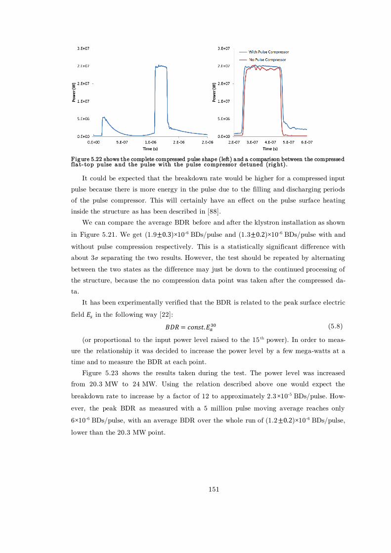
151
Figure 5.22 shows the complete compressed pulse shape (left) and a comparison between the compressed fla t- top pulse and the pulse with the pulse compresso r detuned (right).
It could be expected that the breakdown rate would be higher for a compressed input
pulse because there is more energy in the pulse due to the filling and discharging periods
of the pulse compressor. This will certainly have an effect on the pulse surface heating
inside the structure as has been described in [88].
We can compare the average BDR before and after the klystron installation as shown
in Figure 5.21. We get (1.9±0.3)×10-6 BDs/pulse and (1.3±0.2)×10-6 BDs/pulse with and
without pulse compression respectively. This is a statistically significant difference with
about 3𝜎 separating the two results. However, the test should be repeated by alternating
between the two states as the difference may just be down to the continued processing of
the structure, because the no compression data point was taken after the compressed da-
ta.
It has been experimentally verified that the BDR is related to the peak surface electric
field 𝐸𝑠 in the following way [22]:
𝐵𝐷𝑅 = 𝑐𝑜𝑛𝑠𝑡.𝐸𝑎30 (5.8)
(or proportional to the input power level raised to the 15 th power). In order to meas-
ure the relationship it was decided to increase the power level by a few mega-watts at a
time and to measure the BDR at each point.
Figure 5.23 shows the results taken during the test. The power level was increased
from 20.3 MW to 24 MW. Using the relation described above one would expect the
breakdown rate to increase by a factor of 12 to approximately 2.3×10⁻⁵ BDs/pulse. How-
ever, the peak BDR as measured with a 5 million pulse moving average reaches only
6×10⁻⁶ BDs/pulse, with an average BDR over the whole run of (1.2±0.2)×10-6 BDs/pulse,
lower than the 20.3 MW point.

152
Figure 5.23 shows the high power test from 135 million pulses to 276 million pulses. The input power level (red), a ccumulated number o f breakdowns (green), pulse width a t half maximum (blue) and BDR (bla ck) a re plo tted.
The same effect is seen during the step from 24 MW to 30 MW, which should result
in a 28 fold increase in the BDR according to the relation quoted above. However, the
BDR increases by only a factor of 2.4. This process is repeated, several times during the
run, with the BDR only plateauing after the power has reached around 45 MW after ap-
proximately 257 million pulses. This effect can be explained by the fact that the structure
was still conditioning strongly, with its performance significantly improving before enough
statistics could be collected to measure a reliable BDR.
The power was increased to 46 MW for a short period at the 262 million pulse mark,
but the operation was unstable with the BDR increasing towards 10-4 BDs/pulse. The
power was lowered to 40 MW to stop the BD clustering, and control was handed back to
the conditioning algorithm with a BDR set point of 3×10⁻⁵ BDs/pulse and a target power
of 46 MW. Although the target is reached, the BDR oscillates above and below the set
point, in turn causing the algorithm to ramp and decrease the power level.
The 46 MW power level that was reached appeared to be a hard limit and it was be-
lieved that the structure was now approaching its fully conditioned state. It should now
be possible to try to measure BDR dependencies on power and pulse width because the
structure should condition slowly enough that reliable data points can be taken. It was
decided to first verify the BDR dependency on the pulse width at a fixed power level. In
the literature it is reported that for a constant BDR, the achievable gradient 𝐸𝑎 , is related
to the pulse width 𝜏, in the following way [89]:
𝐸𝑎 = 𝑐𝑜𝑛𝑠𝑡.𝜏−1
6⁄ (5.9)
By combining equations (5.8) and (5.9) it can be shown that for a fixed power lev-
el/electric field the BDR is related to the pulse width 𝜏 in the following way:
𝐵𝐷𝑅 = 𝑐𝑜𝑛𝑠𝑡.𝜏5 (5.10)

153
To test if the crab cavity follows the relation, a run was performed where the power
level was fixed and the pulse width was changed. As shown in Figure 5.24, the power lev-
el was lowered to 43 MW where it was found that the structure could run stably, but
with a sufficiently high breakdown rate that adequate statistics could be gathered within
a few days for each different pulse width.
Figure 5.24 shows the data taken during the constant power run in which the pulse width was va ried. The input power level (red), accumulated number of breakdowns (green), pulse width at half maximum (blue) and BDR (bla ck) a re plo tted.
The first point to be taken was the nominal 200 ns flat top point, followed by a
150 ns run. The pulse width was then briefly increased to 250 ns, where the breakdown
rate increased considerably. This pulse width was held only for 570,000 pulses to reduce
the chance of damage to the structure. Finally, the pulse width was lowered to 100 ns
until the end of the run. The results are summarised in Figure 5.25.
Figure 5.25 shows the FWHM pulse width versus breakdown ra te dependency fo r the crab cavity.
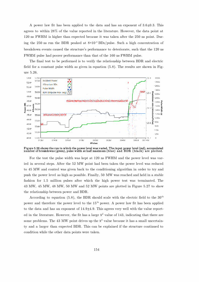
154
A power law fit has been applied to the data and has an exponent of 3.6±0.3. This
agrees to within 28% of the value reported in the literature. However, the data point at
120 ns FWHM is higher than expected because it was taken after the 250 ns point. Dur-
ing the 250 ns run the BDR peaked at 8×10⁻⁴ BDs/pulse. Such a high concentration of
breakdown events caused the structure’s performance to deteriorate, such that the 120 ns
FWHM pulse had poorer performance than that of the 160 ns FWHM pulse.
The final test to be performed is to verify the relationship between BDR and electric
field for a constant pulse width as given in equation (5.8). The results are shown in Fig-
ure 5.26.
Figure 5.26 shows the run in which the power level was varied. The input power level (red), accumulated number of breakdowns (green), pulse width at half maximum (blue) and BDR ( bla ck) a re plo tted.
For the test the pulse width was kept at 120 ns FWHM and the power level was var-
ied in several steps. After the 52 MW point had been taken the power level was reduced
to 45 MW and control was given back to the conditioning algorithm in order to try and
push the power level as high as possible. Finally, 50 MW was reached and held in a stable
fashion for 1.5 million pulses after which the high power test was terminated. The
43 MW, 45 MW, 48 MW, 50 MW and 52 MW points are plotted in Figure 5.27 to show
the relationship between power and BDR.
According to equation (5.8), the BDR should scale with the electric field to the 30 th
power and therefore the power level to the 15 th power. A power law fit has been applied
to the data and has an exponent of 14.9±4.9. This agrees very well with the value report-
ed in the literature. However, the fit has a large Χ2 value of 143, indicating that there are
some problems. The 43 MW point drives up the Χ2 value because it has a small uncertain-
ty and a larger than expected BDR. This can be explained if the structure continued to
condition while the other data points were taken.
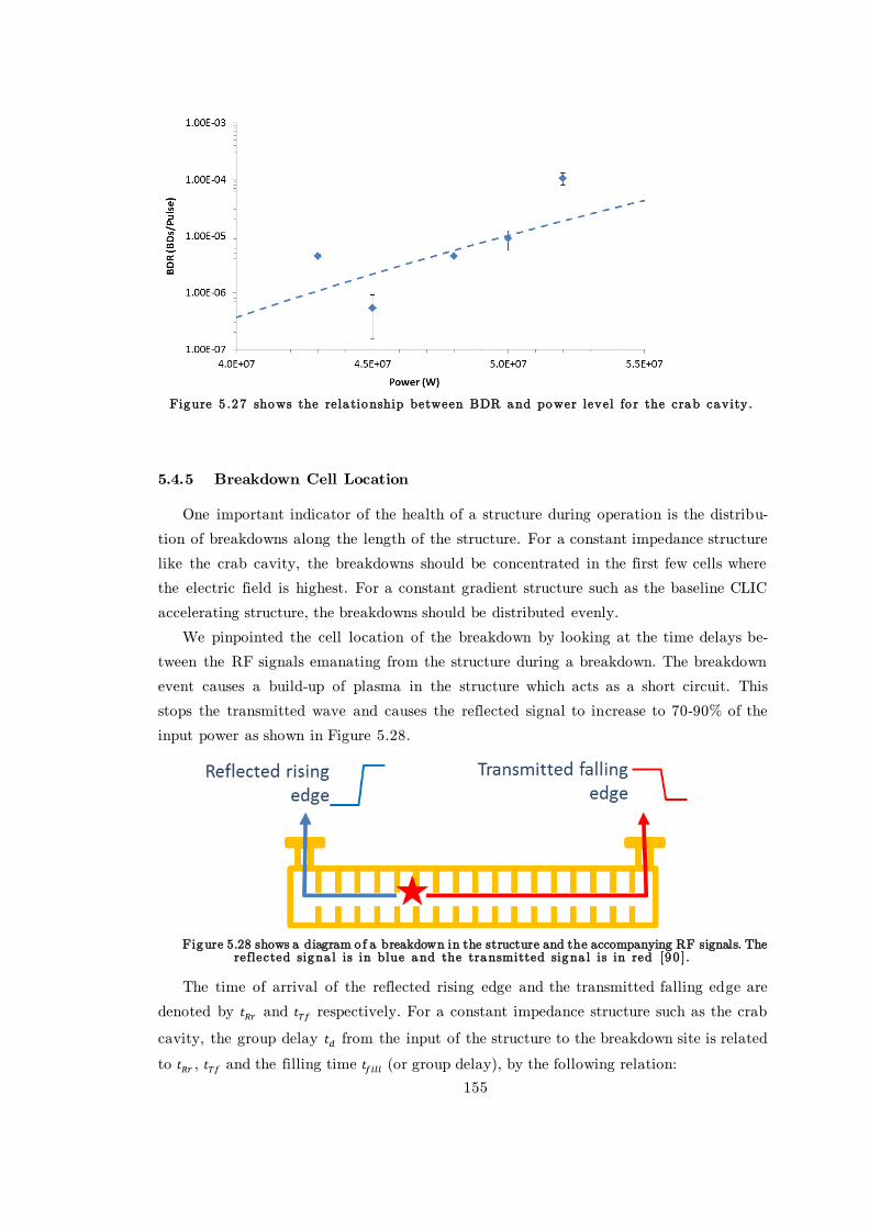
155
Figure 5 .27 shows the rela tionship between BDR and power level fo r the crab cavity.
5.4.5 Breakdown Cell Location
One important indicator of the health of a structure during operation is the distribu-
tion of breakdowns along the length of the structure. For a constant impedance structure
like the crab cavity, the breakdowns should be concentrated in the first few cells where
the electric field is highest. For a constant gradient structure such as the baseline CLIC
accelerating structure, the breakdowns should be distributed evenly.
We pinpointed the cell location of the breakdown by looking at the time delays be-
tween the RF signals emanating from the structure during a breakdown. The breakdown
event causes a build-up of plasma in the structure which acts as a short circuit. This
stops the transmitted wave and causes the reflected signal to increase to 70-90% of the
input power as shown in Figure 5.28.
Figure 5.28 shows a diagram o f a breakdown in the structure and the accompanying RF signals. The reflected signa l is in blue and the transmitted signa l is in red [90 ].
The time of arrival of the reflected rising edge and the transmitted falling edge are
denoted by 𝑡𝑅𝑟 and 𝑡𝑇𝑓 respectively. For a constant impedance structure such as the crab
cavity, the group delay 𝑡𝑑 from the input of the structure to the breakdown site is related
to 𝑡𝑅𝑟 , 𝑡𝑇𝑓 and the filling time 𝑡𝑓𝑖𝑙𝑙 (or group delay), by the following relation:
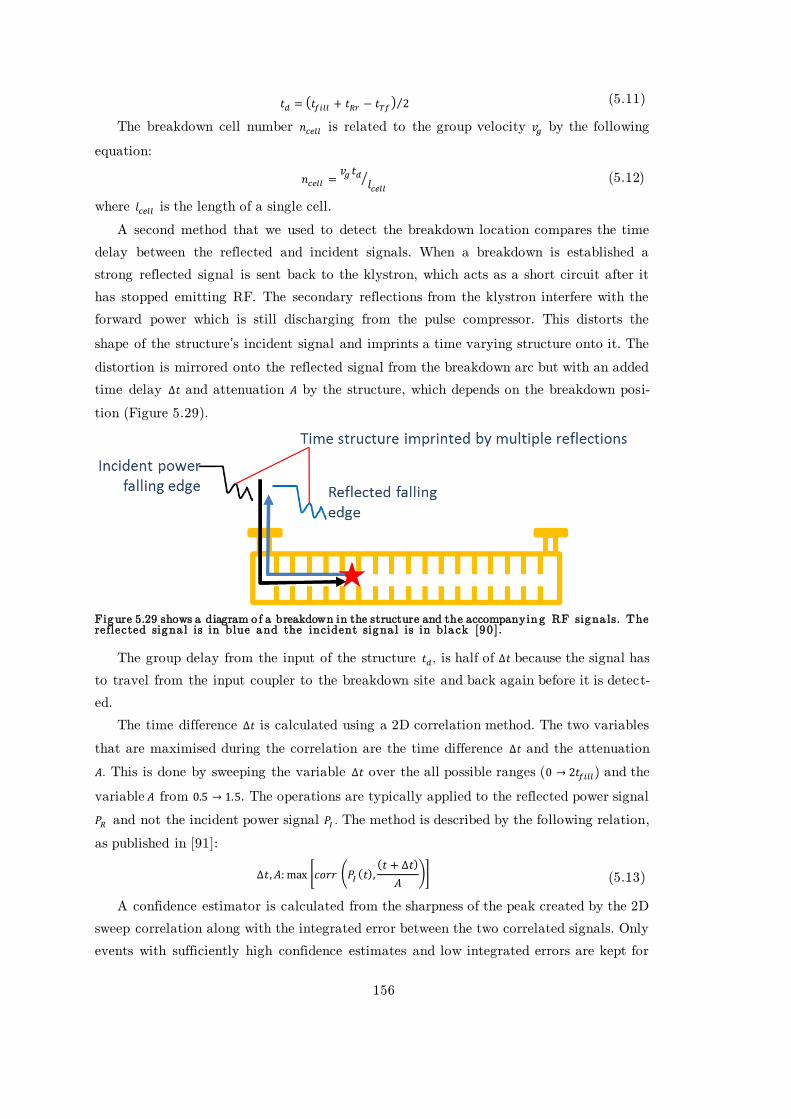
156
𝑡𝑑 = (𝑡𝑓𝑖𝑙𝑙 + 𝑡𝑅𝑟 − 𝑡𝑇𝑓) 2⁄ (5.11)
The breakdown cell number 𝑛𝑐𝑒𝑙𝑙 is related to the group velocity 𝑣𝑔 by the following
equation:
𝑛𝑐𝑒𝑙𝑙 =𝑣𝑔 𝑡𝑑
𝑙𝑐𝑒𝑙𝑙⁄ (5.12)
where 𝑙𝑐𝑒𝑙𝑙 is the length of a single cell.
A second method that we used to detect the breakdown location compares the time
delay between the reflected and incident signals. When a breakdown is established a
strong reflected signal is sent back to the klystron, which acts as a short circuit after it
has stopped emitting RF. The secondary reflections from the klystron interfere with the
forward power which is still discharging from the pulse compressor. This distorts the
shape of the structure’s incident signal and imprints a time varying structure onto it. The
distortion is mirrored onto the reflected signal from the breakdown arc but with an added
time delay ∆𝑡 and attenuation 𝐴 by the structure, which depends on the breakdown posi-
tion (Figure 5.29).
Figure 5.29 shows a diagram o f a breakdown in the structure and the accompanyin g RF signa ls. The reflected signa l is in blue and the incident signa l is in bla ck [90 ].
The group delay from the input of the structure 𝑡𝑑, is half of ∆𝑡 because the signal has
to travel from the input coupler to the breakdown site and back again before it is detect-
ed.
The time difference ∆𝑡 is calculated using a 2D correlation method. The two variables
that are maximised during the correlation are the time difference ∆𝑡 and the attenuation
𝐴. This is done by sweeping the variable ∆𝑡 over the all possible ranges (0 → 2𝑡𝑓𝑖𝑙𝑙) and the
variable 𝐴 from 0.5 → 1.5. The operations are typically applied to the reflected power signal
𝑃𝑅 and not the incident power signal 𝑃𝐼 . The method is described by the following relation,
as published in [91]:
∆𝑡, 𝐴: max [𝑐𝑜𝑟𝑟 (𝑃𝐼 (𝑡),(𝑡 + ∆𝑡)
𝐴)] (5.13)
A confidence estimator is calculated from the sharpness of the peak created by the 2D
sweep correlation along with the integrated error between the two correlated signals. Only
events with sufficiently high confidence estimates and low integrated errors are kept for
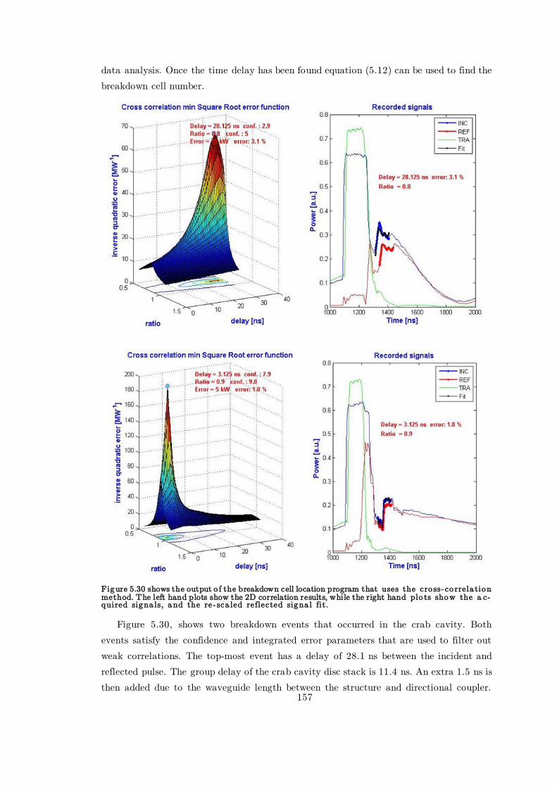
157
data analysis. Once the time delay has been found equation (5.12) can be used to find the
breakdown cell number.
Figure 5.30 shows the output o f the breakdown cell location program that uses the cro ss-co rrela tion method. The left hand plots show the 2D correlation results, while the right hand plo ts show the a c-quired signa ls, and the re - sca led reflected signa l fit.
Figure 5.30, shows two breakdown events that occurred in the crab cavity. Both
events satisfy the confidence and integrated error parameters that are used to filter out
weak correlations. The top-most event has a delay of 28.1 ns between the incident and
reflected pulse. The group delay of the crab cavity disc stack is 11.4 ns. An extra 1.5 ns is
then added due to the waveguide length between the structure and directional coupler.
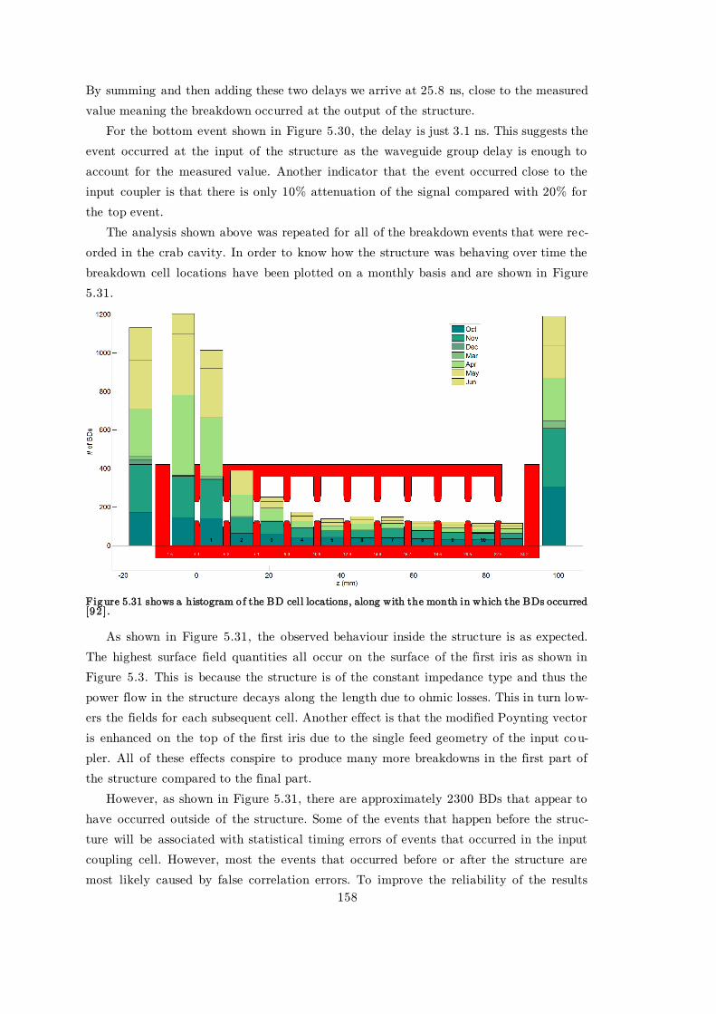
158
By summing and then adding these two delays we arrive at 25.8 ns, close to the measured
value meaning the breakdown occurred at the output of the structure.
For the bottom event shown in Figure 5.30, the delay is just 3.1 ns. This suggests the
event occurred at the input of the structure as the waveguide group delay is enough to
account for the measured value. Another indicator that the event occurred close to the
input coupler is that there is only 10% attenuation of the signal compared with 20% for
the top event.
The analysis shown above was repeated for all of the breakdown events that were rec-
orded in the crab cavity. In order to know how the structure was behaving over time the
breakdown cell locations have been plotted on a monthly basis and are shown in Figure
5.31.
Figure 5.31 shows a histogram o f the BD cell locations, along with the month in which the BDs occurred [92 ].
As shown in Figure 5.31, the observed behaviour inside the structure is as expected.
The highest surface field quantities all occur on the surface of the first iris as shown in
Figure 5.3. This is because the structure is of the constant impedance type and thus the
power flow in the structure decays along the length due to ohmic losses. This in turn low-
ers the fields for each subsequent cell. Another effect is that the modified Poynting vector
is enhanced on the top of the first iris due to the single feed geometry of the input cou-
pler. All of these effects conspire to produce many more breakdowns in the first part of
the structure compared to the final part.
However, as shown in Figure 5.31, there are approximately 2300 BDs that appear to
have occurred outside of the structure. Some of the events that happen before the struc-
ture will be associated with statistical timing errors of events that occurred in the input
coupling cell. However, most the events that occurred before or after the structure are
most likely caused by false correlation errors. To improve the reliability of the results
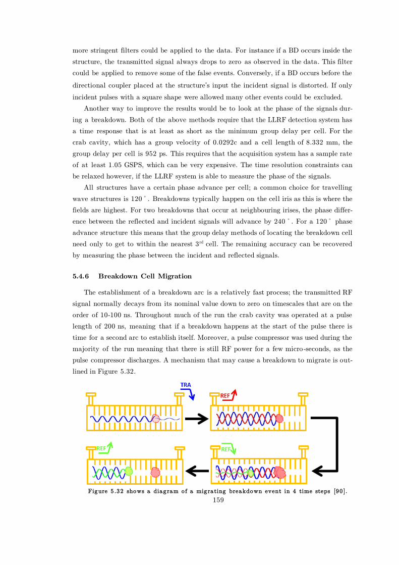
159
more stringent filters could be applied to the data. For instance if a BD occurs inside the
structure, the transmitted signal always drops to zero as observed in the data. This filter
could be applied to remove some of the false events. Conversely, if a BD occurs before the
directional coupler placed at the structure’s input the incident signal is distorted. If only
incident pulses with a square shape were allowed many other events could be excluded.
Another way to improve the results would be to look at the phase of the signals dur-
ing a breakdown. Both of the above methods require that the LLRF detection system has
a time response that is at least as short as the minimum group delay per cell. For the
crab cavity, which has a group velocity of 0.0292c and a cell length of 8.332 mm, the
group delay per cell is 952 ps. This requires that the acquisition system has a sample rate
of at least 1.05 GSPS, which can be very expensive. The time resolution constraints can
be relaxed however, if the LLRF system is able to measure the phase of the signals.
All structures have a certain phase advance per cell; a common choice for travelling
wave structures is 120º. Breakdowns typically happen on the cell iris as this is where the
fields are highest. For two breakdowns that occur at neighbouring irises, the phase differ-
ence between the reflected and incident signals will advance by 240º. For a 120º phase
advance structure this means that the group delay methods of locating the breakdown cell
need only to get to within the nearest 3rd cell. The remaining accuracy can be recovered
by measuring the phase between the incident and reflected signals.
5.4.6 Breakdown Cell Migration
The establishment of a breakdown arc is a relatively fast process; the transmitted RF
signal normally decays from its nominal value down to zero on timescales that are on the
order of 10-100 ns. Throughout much of the run the crab cavity was operated at a pulse
length of 200 ns, meaning that if a breakdown happens at the start of the pulse there is
time for a second arc to establish itself. Moreover, a pulse compressor was used during the
majority of the run meaning that there is still RF power for a few micro-seconds, as the
pulse compressor discharges. A mechanism that may cause a breakdown to migrate is out-
lined in Figure 5.32.
Figure 5 .32 shows a diag ram o f a mig ra ting breakdown event in 4 time steps [90 ].
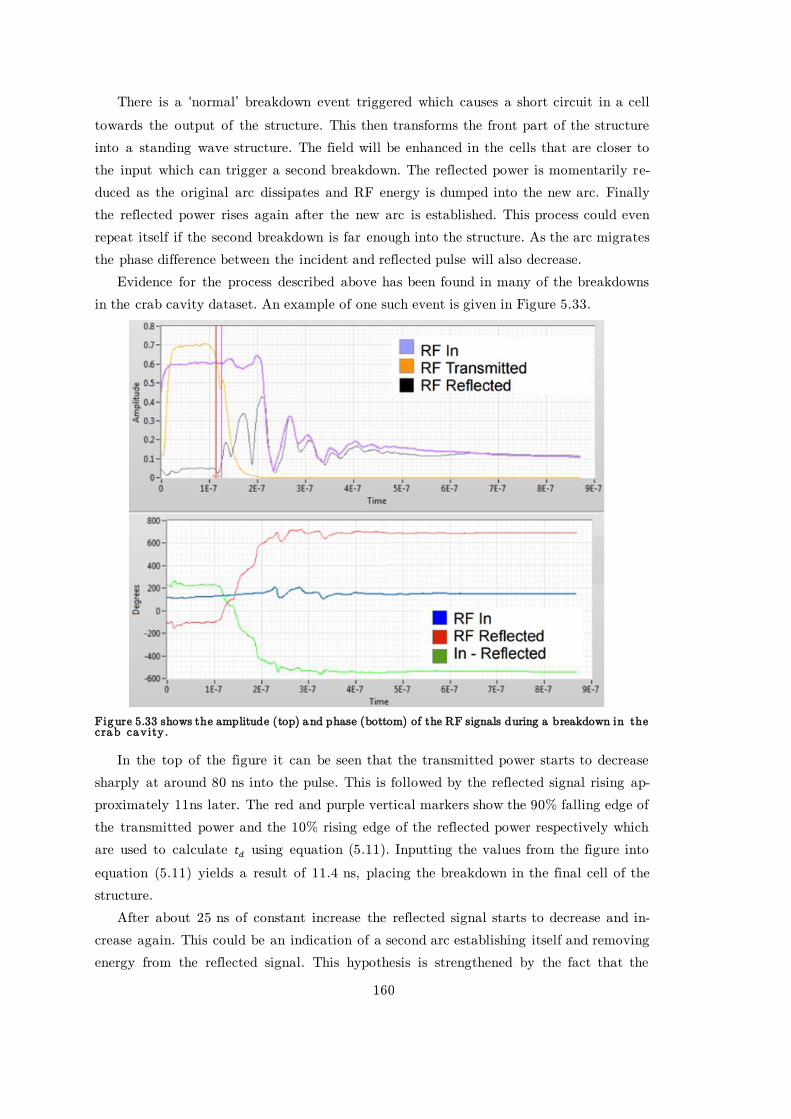
160
There is a ‘normal’ breakdown event triggered which causes a short circuit in a cell
towards the output of the structure. This then transforms the front part of the structure
into a standing wave structure. The field will be enhanced in the cells that are closer to
the input which can trigger a second breakdown. The reflected power is momentarily re-
duced as the original arc dissipates and RF energy is dumped into the new arc. Finally
the reflected power rises again after the new arc is established. This process could even
repeat itself if the second breakdown is far enough into the structure. As the arc migrates
the phase difference between the incident and reflected pulse will also decrease.
Evidence for the process described above has been found in many of the breakdowns
in the crab cavity dataset. An example of one such event is given in Figure 5.33.
Figure 5.33 shows the amplitude (top) and phase (bottom) of the RF signals during a breakdown in the crab cavity.
In the top of the figure it can be seen that the transmitted power starts to decrease
sharply at around 80 ns into the pulse. This is followed by the reflected signal rising ap-
proximately 11ns later. The red and purple vertical markers show the 90% falling edge of
the transmitted power and the 10% rising edge of the reflected power respectively which
are used to calculate 𝑡𝑑 using equation (5.11). Inputting the values from the figure into
equation (5.11) yields a result of 11.4 ns, placing the breakdown in the final cell of the
structure.
After about 25 ns of constant increase the reflected signal starts to decrease and in-
crease again. This could be an indication of a second arc establishing itself and removing
energy from the reflected signal. This hypothesis is strengthened by the fact that the
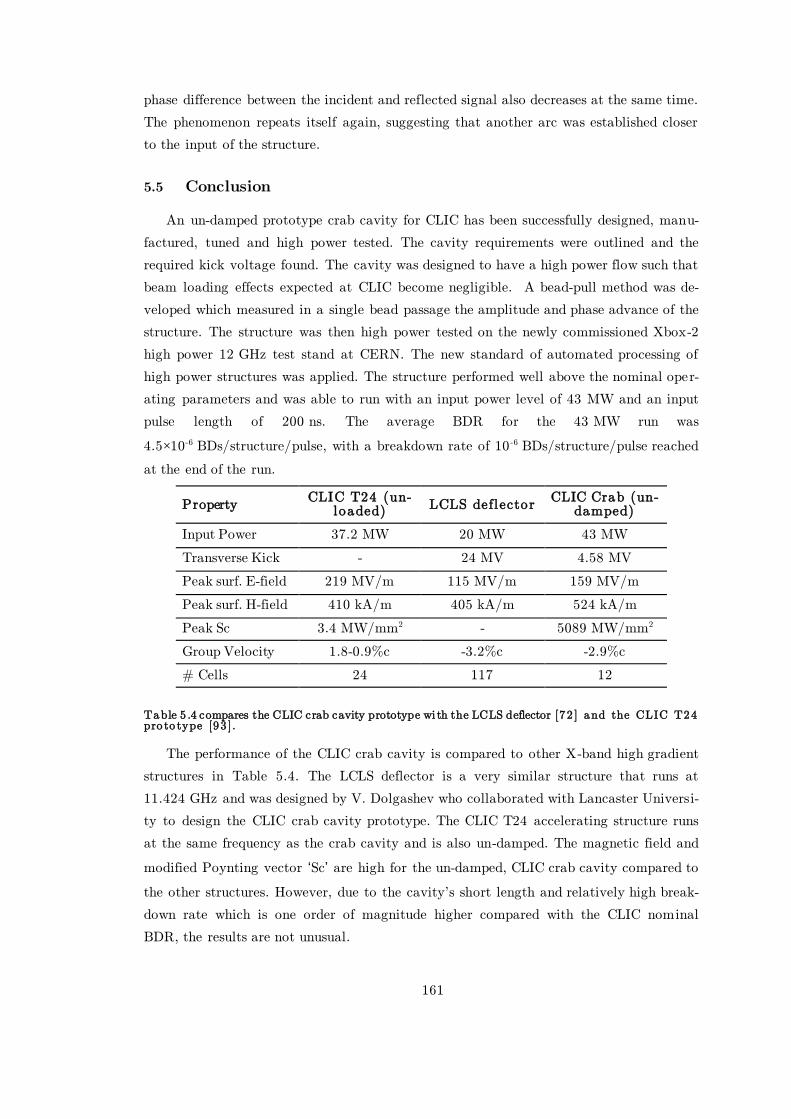
161
phase difference between the incident and reflected signal also decreases at the same time.
The phenomenon repeats itself again, suggesting that another arc was established closer
to the input of the structure.
5.5 Conclusion
An un-damped prototype crab cavity for CLIC has been successfully designed, manu-
factured, tuned and high power tested. The cavity requirements were outlined and the
required kick voltage found. The cavity was designed to have a high power flow such that
beam loading effects expected at CLIC become negligible. A bead-pull method was de-
veloped which measured in a single bead passage the amplitude and phase advance of the
structure. The structure was then high power tested on the newly commissioned Xbox-2
high power 12 GHz test stand at CERN. The new standard of automated processing of
high power structures was applied. The structure performed well above the nominal oper-
ating parameters and was able to run with an input power level of 43 MW and an input
pulse length of 200 ns. The average BDR for the 43 MW run was
4.5×10⁻⁶ BDs/structure/pulse, with a breakdown rate of 10 -6 BDs/structure/pulse reached
at the end of the run.
Property CLIC T24 (un-
loaded) LCLS deflector
CLIC Crab (un-damped)
Input Power 37.2 MW 20 MW 43 MW
Transverse Kick - 24 MV 4.58 MV
Peak surf. E-field 219 MV/m 115 MV/m 159 MV/m
Peak surf. H-field 410 kA/m 405 kA/m 524 kA/m
Peak Sc 3.4 MW/mm2 - 5089 MW/mm2
Group Velocity 1.8-0.9%c -3.2%c -2.9%c
# Cells 24 117 12
Table 5 .4 compares the CLIC crab cavity prototype wi th the LCLS deflector [72 ] and the CLIC T24 pro to type [93 ].
The performance of the CLIC crab cavity is compared to other X-band high gradient
structures in Table 5.4. The LCLS deflector is a very similar structure that runs at
11.424 GHz and was designed by V. Dolgashev who collaborated with Lancaster Universi-
ty to design the CLIC crab cavity prototype. The CLIC T24 accelerating structure runs
at the same frequency as the crab cavity and is also un-damped. The magnetic field and
modified Poynting vector ‘Sc’ are high for the un-damped, CLIC crab cavity compared to
the other structures. However, due to the cavity's short length and relatively high break-
down rate which is one order of magnitude higher compared with the CLIC nominal
BDR, the results are not unusual.
162
Chapter 6
6 Conclusions
This thesis outlines the work which was undertaken to set up multiple high power X-
band test stands at CERN. The development of the second X-band test stand at CERN,
Xbox-2 was followed from inception to completion. The LLRF system, interlock system
and control algorithms have all been designed and validated. Ultimately, the completed
test stand Xbox-2 was used to test the Lancaster designed CLIC crab cavity prototype.
6.1 High Power X-band test Stands at CERN
6.1.1 Xbox-1
The design and commissioning of the first test stand at CERN was not covered in this
body of work. However, significant improvements to the control system and operation of
the test stand were completed. Calibration techniques were developed and then used to
improve the accuracy of all of the power measurements taken.
The pulse compressor at Xbox-1 uses tuning pistons to change the resonant frequency
of each of the two storage cavities. The tuning was performed manually and required an
operator in order to run the experiment. A tuning algorithm was developed in order to
maintain a good shape of the compressed pulse and to keep the reflected power to the
klystron at safe levels. This ultimately allowed the test stand to operate 24 hours per day.
The pulse forming network was upgraded such that the resolution of the power output
was improved by a factor of 256 and the communication speed was enhanced by a factor
of 50. Both of these changes allowed the system to automatically control the power level
to a given set point using a PID loop.
The addition of a reliable power feedback loop allowed the development of a higher
software layer to control the power set point. This conditioning algorithm allows struc-
tures to be processed with a constant BDR and ensures that the structure is protected if
the breakdown rate is too high. Use of this algorithm is now the standard procedure for
conditioning all CLIC prototype structures.
6.1.2 Xbox-2
The second high power test stand at CERN used the experience gained at Xbox-1 to
implement an improved system. The work completed focussed on the creation of a new
LLRF and control system based on the PXI platform. The LLRF generation was im-
proved by utilising a 200 MHz bandwidth vector generator and up-mixing scheme, allow-
ing for fast phase feedback algorithms to be developed, such as the pulse flattening feed-
back algorithm for the pulse compressor. The re-designed RF acquisition system used a
163
400 MHz IF direct sampling scheme to increase performance. This allowed the phase and
amplitude of the signals to be measured, without the errors associated with physical IQ
demodulators.
Interlocking from the acquisition of the RF signals, vacuum system and safety and ac-
cess systems was implemented through the PXI crate and modulator control system. A
trigger and timing distribution system was developed through an FPGA directly tied to
the interlock sources to increase safety by reducing the risk of machine damage due to
software crashes.
Tuning of a new design of a SLED I pulse compressor was performed in the laborato-
ry. After which its performance was verified through measurements in both the frequency
and time domains. The test stand was commissioned up to high power, during which a
new vacuum feedback algorithm was developed which controlled the power level, while
keeping the pressure level inside the waveguide network constant.
6.1.3 Xbox-3
The general layout of the third high power test stand at CERN was presented and its
importance in increasing testing capacity was highlighted. Designs for the LLRF and con-
trol systems have been completed based on an expansion and upgrade of the Xbox-2
LLRF system. The first of the modulator/klystron units from Toshiba and Scandinova
have been tested on site and perform to expectations. The two way combination scheme
has been fully verified at low power using a scaled down version of the LLRF system, a
coaxial -3 dB hybrid and the Xbox-2 pulse compressor. During this test the hardware and
software controls needed to switch the RF power to two different DUTs was developed.
6.1.4 CLIC Crab Cavity Prototype
The CLIC crab cavity prototype’s requirements were considered and the RF design
was verified through re-simulation of the cavity fields using HFSS. A novel tuning method
was developed using just a dielectric bead which measures in a single bead passage the
amplitude and phase advance per cell of deflecting mode travelling wave structures. This
method was successfully used to tune the crab cavity such that the average phase ad-
vance per cell was 120° ± 0.1° with a maximum deviation of less than ±1°.
The structure was the first structure to be high power tested on the newly commis-
sioned Xbox-2. The test stand performed well by using the structure conditioning algo-
rithm and interlock system to safely take the crab cavity to a peak power level of 51 MW
with a 150 ns pulse width. The cavity was able to run stably at 43 MW and 200 ns with
a breakdown rate of 10 -6 BDs/pulse. This power level is well above the nominal design
parameters of 13.35 MW at 200 ns pulse width.
164
6.2 Future Work
6.2.1 Xbox-3 Commissioning
While much of the design work and procurement for Xbox-3 has been completed,
there are some outstanding issues. The LLRF crates need to be assembled from the con-
nectorised components and tested. Much of the high power RF components such as the
pulse compressors and waveguides are still under manufacture. The software developed
for the single klystron test described in section 4.9.2 must be modified to incorporate the
phase manipulations that were tested in the laboratory as described in section 4.4. This
will allows the switching of the RF power between each of the two test slots at a repeti-
tion rate of 200 Hz. More complex interlocking systems must also be developed as there
are more failure modes when combing 2 klystrons compared to a single klystron test
stand. For example, if one of a pair of klystrons trips the other klystron must be immedi-
ately stopped, because -3 dB hybrid power combination scheme only works if both of the
hybrid’s inputs receive RF power. Finally, the system must be conditioned up to full pow-
er in order to validate that all of the new waveguide components can withstand 50 MW
pulses at pulse repetition rates up to 200 Hz.
6.2.2 CLIC Crab Cavity Post Mortem Analysis
A map of the surface fields inside the crab cavity was produced in section 5.1.3. The
surface electric and magnetic fields and the modified Poynting vector were calculated. Of
particular interest are the distributions of the various fields around the iris. Unlike an
accelerating structure which has high electric and magnetic fields distributed uniformly
around the iris, the crab cavities deflecting mode has the fields separated onto the vertical
and horizontal planes. The modified Poynting vector which is believed to play an im-
portant role in surface breakdown phenomena is distributed at four points on the iris at
45º to the maximum electric and magnetic fields. This unique field profile will allow an
unprecedented study into the source of breakdown events via a post mortem inspection.
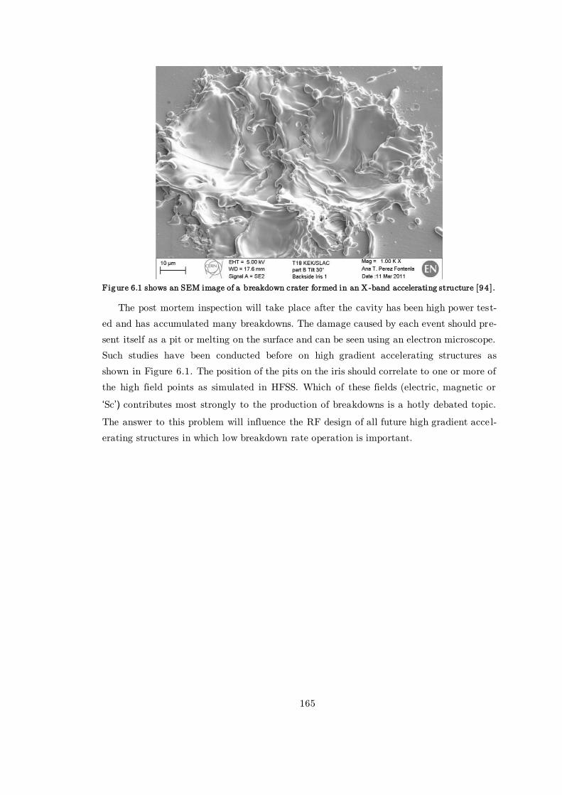
165
Figure 6.1 shows an SEM image of a breakdown crater formed in an X-band accelerating structure [94 ].
The post mortem inspection will take place after the cavity has been high power test-
ed and has accumulated many breakdowns. The damage caused by each event should pre-
sent itself as a pit or melting on the surface and can be seen using an electron microscope.
Such studies have been conducted before on high gradient accelerating structures as
shown in Figure 6.1. The position of the pits on the iris should correlate to one or more of
the high field points as simulated in HFSS. Which of these fields (electric, magnetic or
‘Sc’) contributes most strongly to the production of breakdowns is a hotly debated topic.
The answer to this problem will influence the RF design of all future high gradient acce l-
erating structures in which low breakdown rate operation is important.

166
Bibliography
[1] L. Evans, P. Bryant, LHC Machine. Journal of Instrumentation, vol. 3, S08001
(2008).
[2] L.M. Lederman, The Tevatron. Scientific American, vol. 234, no. 03, pp. 48-
55, (1991).
[3] H. Murayama, M. E. Peskin, Physics opportunities of e+ e-linear colliders.
arXiv preprint hep-ex/9606003, 1996.
[4] A.D. Martin, W.J. Stirling, R.S. Thorne, G. Watt, Parton distributions for the
LHC. The European Physical Journal C, vol. 63, no. 2, pp. 189-285, (2009).
[5] H. Yamamoto. Newsline: The Newsletter of the Linear Collider Community.
[Online resource], (2015, July).
http://newsline.linearcollider.org/2015/07/09/ilc-the-discovery-machine/
[6] R. W. Assmann, Frank Zimmermann. Polarization issues at CLIC. CERN-SL-
2001-064-AP. (2001).
[7] G. Moortgat-Pick, Polarized Beams for Top, Higgs and SUSY Searches.
CERN-PH-TH/2005-138, (2005).
[8] D. Brandt, H. Burkhardt, M. Lamont, S. Myers, J. Wenninger, Accelerator
Physics at LEP Reports on Progress in Physics, vol. 63, no. 6, pp. 939–1000,
(2000).
[9] D. Boussard, Performance of the LEP2 SRF system. Proceedings of the
Particle Accelerator Conference 1997, vol.3, pp.2879-2883, (1997).
[10] M Bogomilov, Y Karadzhov, D Kolev, I Russinov, R Tsenov, et al. The MICE
Muon Beam on ISIS and the beam-line. Journal of Instrumentation, vol. 7,
P05009, (2012).
[11] S. Geer, Muon colliders and neutrino factories. Proceedings of Linear
Accelerator Conference LINAC2010, Tsukuba, Japan, pp. 1048-1052, (2010).
[12] J. Delahaye, A. De Roeck, G. Geschonke, H. Braun, CLIC here for the future.
CERN Courier, vol. 48, no. 7, (2008).
[13] R.L. Geng, Review of new shapes for higher gradients. Physica C:
Superconductivity, vol. 441, no. 1-2, pp. 145-150, (2006).
[14] V.A. Dolgashev, S.G. Tantawi, A.D. Yeremian, Z. Li, Y.Higashi, B.Spataro,
Status of High Power Tests of Normal Conducting Short Standing Wave
Structures Proceedings of International Particle Accelerator Conference
IPAC2011, San Sebastian, Spain, pp. 241-243, (2011).
[15] M. Aicheler, P. Burrows, M. Draper, T. Garvey, P. Lebrun, et al., A Multi-
167
TeV Linear Collider based on CLIC Technology: CLIC Conceptual Design
Report. JAI-2012-001, (2012).[Online resource].
https://edms.cern.ch/document/1234244/
[16] A. Grudiev, D. Schulte, W. Wuensch, Optimum frequency and gradient for
the CLIC main linac accelerating structure. CERN-AB-2006-028, (2006).
[17] W. Wuensch, C. Achard, S. Dobert, H. H. Braun, I. Syratchev, et al. A
Demonstration of High-Gradient Acceleration. 20th IEEE Particle Accelerator
Conference, Portland, OR, USA, pp.495 (2003).
[18] S. T. Heikkinen, S. Calatroni, H. Neupert, Thermal Fatigue Issues in High
Gradient Particle Accelerators. No. CERN-OPEN-2006-004. (2006).
[19] W. Wuensch, Progress in Understanding the High-Gradient Limitations.
Proceedings of APAC 2007, Raja Ramanna Centre for Advanced
Technology(RRCAT), Indore, India, (2007).
[20] D. Schulte, Luminosity Limitations at the Multi-TeV Linear Collider.
Proceedings of EPAC 2002, Paris, France, (2002).
[21] A. Descoeudres, Y. Levinsen, S. Calatroni, M. Taborelli, W. Wuensch,
Investigation of the dc vacuum breakdown mechanism. Physical Review
Special Topics-Accelerators and Beams, vol. 12.9, no. 9, pp. 092001, (2009).
[22] A. Grudiev, S. Calatroni, and W. Wuensch, New local field quantity
describing the high gradient limit of accelerating structures. Physical Review
Special Topics-Accelerators and Beams, vol. 12, no. 10, pp. 102001, (2009).
[23] R Zennaro, Study of the machining and assembly tolerances for the CLIC
accelerating structure. EUROTeV-Report-2008-081, (2008).
[24] J. W. Wang, J. R. Lewandowski, J. W. Van Pelt, C. Yoneda, G. Riddone, et
al. Fabrication technologies of the high gradient accelerator structures at
100MV/m range. Proceedings of IPAC10, Kyoto, Japan, (2010).
[25] T Higo, Performance of CLIC prototype accelerator structures tested at
Nextef. at CLIC Workshop 2014, Geneva, Switzerland, (2014).
[26] P. Lebrun, L. Linssen, A. Lucaci-Timoce, D. Schulte, F. Simon, S. Stapnes, et
al., The CLIC Programme: Towards a Staged e+e- Linear Collider Exploring
the Terascale : CLIC Conceptual Design Report CERN, Geneva, ANL-HEP-
TR-12-51, CERN-2012-005, KEK Report 2012-002, MPP-2012-015, (2012).
[27] A. Vlieks, "X-Band Klystron Development at SLAC. Stanford Linear
Accelerator Center, USA, SLAC-PUB-13741, (2009).
[28] N. Catalan-Lasheras, A. Degiovanni, S. Doebert, W. Farabolini, J. Kover-
mann, et al. Experience operating an X-band high-power test stand at CERN.
Proceedings of IPAC2014, Dresden, Germany, (2014).
168
[29] A.A. Bogdashov, G.G. Denisov, S.V. Kuzikov, A.A. Vikharev, K.M. Schirm,
I. Syratchev, A 12 GHz Pulse Compressor and Components for CLIC Test
Stand. Proceedings of RuPAC2010, pp. 44-46, (2010).
[30] R. B. Palmer, Energy Scaling, Crab crossing and the pair probelm, Stanford
Linear Accelerator Center, Stanford University, Stanford, California, SLAC-
PUB-4707, (1988).
[31] The Compact Linear Collider Study. [Online resource]. (2010, April)
http://clic-meeting.web.cern.ch/clic-meeting/clictable2010.html
[32] G. Burt, P. Ambattu, I. Tahir, A. Dexter, EuCARD Milestone Report: CLIC
crab cavity LLRF. University of Lancaster, (2011).
[33] A. Dexter, G. Burt, P. Ambattu, V. Dolgashev, A. Grudiev, I. Shinton, CLIC
Crab Cavities. at LCWS11, Granada, Spain, (2011).
[34] G. Burt, P.K. Ambattu, C. Lingwood, T. Abram, I. Burrows, et al., Design
and operation of a compact 1 MeV X-band Linac. Proceedings of LINAC2012,
Tel-Aviv, Israel, (2012).
[35] M. L. Meurk,D. A. Goer, G. Spalek, T. Cook, The Mobetron: A New Concept
for Intraoperative Radiotherapy," Proceedings of the 6th International IORT
Symposium, San Fransisco, CA, (1996).
[36] R. A., Marsh, G. Anderson, S.G. Anderson, S.M. Betts, S.E. Fisher, et al.
LLNL X-band Test Station Commissioning and X-ray Status Proceedings of
IPAC14, Dresden, Germany, (2014).
[37] P. Emma, X-Band RF Harmonic Compensation for Linear Bunch
Compression in the LCLS. SLAC, Stanford, CA, SLAC-TN-2005-004. LCLS-
TN-01-1, (2001).
[38] G.L. Orlandi, M.Aiba, F.Baerenbold, S.Bettoni, B.Beutner, et al.
Characterization of Compressed Bunches in the SwissFEL Injector Test
Facility. Proceedings of IBIC2013, Oxford, UK, (2013).
[39] G D'Auria, S Di Mitri, G Penco, and C Serpico, RF Activation and
Preliminary Beam Tests of the X-band Linearizer at the FERMI@Elettra
FEL Project. Proceedings of IPAC2012, New Orleans, Louisiana, USA (2012).
[40] J. M. Byrd, L. Doolittle, G. Huang, J. W. Staples, R. Wilcox, et al.
Femtosecond synchronization of laser systems for the LCLS. Proceedings of
BIW10, Santa Fe, New Mexico, US, (2010).
[41] ANSYS Inc. HFSS. [Online resource]
http://www.ansys.com/Products/Simulation+Technology/Electronics/Signal
+Integrity/ANSYS+HFSS
[42] R Ruber, V Ziemann, T Ekelof, A. Palaia, W. Farabolini, R. Corsini, The

169
CTF3 Two-beam Test Stand. Nuclear Instruments and Methods in Physics
Research Section A: Accelerators, Spectrometers, Detectors and Associated
Equipment, vol. 729, pp. 546-553, (November 2013).
[Online resource]. http://dx.doi.org/10.1016/j.nima.2013.07.055.
[43] A Palaia, M Jacewicz, R Ruber, V Ziemann, W Farabolini, Effects of rf
breakdown on the beam in the Compact Linear Collider prototype accelerator
structure. Physical Review ST Accelerators and Beams, vol. 16, 8, pp.
081004, (August 2013.)
[Online]. http://link.aps.org/doi/10.1103/PhysRevSTAB.16.081004
[44] D. Schulte, A. Grudiev, Ph. Lebrun, G. McMonagle, I. Syratchev, W.
Wuensch, Exploration of a klystron-powered first energy stage of CLIC.
CERN, CERN-OPEN-2013-024, (2012).
[45] T Higo, T. Abe, Y. Arakida, S. Matsumoto, T. Shidara, et al. Comparison of
high gradient performance in varying cavity geometries. Proceedings of
IPAC2013, Shanghai, China, (2013).
[46] C. Adolphsen, Normal-Conducting RF Structure Test Facilities and Results.
Proceedings of PAC 2003, Portland, OR, USA, (2003).
[47] D. Sprehn, A. Haase, A. Jensen, E. N. Jongewaard, C. D. Nantista ,et al. A
12 GHz 50 MW klystron for support of accelerator research. Proceedings of
IPAC2010, Kyoto, Japan, (2010).
[48] R. H. Varian, S. F. Varian, A high frequency oscillator and amplifier. Journal
of Applied Physics, vol. 10, 5, pp. 321-327, (1939).
[49] D. Farkas, H. A. Hogg, G. A. Loew, and P. B. Wilson, "SLED: A Method for
Doubling SLAC's Energy. Proceedings of the 9th Int. Conf. on High Energy
Accelerators, (1974).
[50] A. Fiebig, C. Schieblich, A SLED type pulse compressor with rectangular
pulse shape. CERN, Geneva, CERN-PS-90-13-RF. CM-P00059378, (1990).
[51] S. V. Kuzikov, G. Denisov, S. Heikkenen, J.L. Hirshfield, G.I. Kalynova, et
al. Study of Ka-Band High-Power Transmission Lines. in AIP Conference
Proceedings, 7th Workshop on High Energy Density and High Power RF,
Vol. 807, pp. 424-430, (2006).
[52] National Instruments, [Online resource] http://www.ni.com/
[53] F Tecker, R. Corsini, M. Dayyani Kelisani, S. Doebert, A. Grudiev, et al.
Experimental Study of the Effect of Beam Loading on RF Breakdown Rate in
CLIC High-Gradient Accelerating Structures. Proceedings of IPAC2013,
Shanghai, China, (2013).
[54] W Wuensch, Observations about RF Breakdown from the CLIC High

170
Gradient Testing Program. in AIP Conference Proceedings, vol. 877, 12th
Workshop on Advanced Accelerator Concepts, pp. 15-21. (2006)
[55] VDL Systems. [Online resource]. http://www.vdlsystems.nl/
[56] D. Gudkov, S. Lebet, R. Leuxe, A. Olyunin, G. Riddone, et al. General
purpose X-band High RF power components developed within CLIC
collaboration. Proceedings of the International Workshop on Breakdown
Science and High Gradient Technology, KEK, Tsukuba, (2012).
[57] G. F. Engen, C. A. Hoer, Thru-Reflect-Line: An improved technique for
calibrating the dual six-port automatic network analyzer. IEEE Transactions
Microwave Theory and Techniques, vol. 27, 12, pp. 987-992, December 1979.
[58] L. G. Hector, H. L. Schultz, The Dielectric Constant of Air at
Radiofrequencies. Journal of Applied Physics, vol. 7, no. 4, pp. 133, (1936).
[59] Altium Limited. Altium Designer. [Online resource].
http://www.altium.com/altium-designer/overview
[60] I. Syratchev, Private Communication, (2014).
[61] I. Syratchev, X-band high RF power testing activity at CERN. at EnEfficient
RF Sources Workshop, Daresbury, UK, (2014).
[62] N. Catalan Lasheras, Progress on XBox-2 and 3. at CLIC Workshop 2014,
Geneva, Switzerland, (2014).
[Online resource].
https://indico.cern.ch/event/275412/session/8/contribution/38/attachments/
498814/689081/Xboxes_CLICWS_Feb2014.pdf
[63] I. Syratchev, Status of high-power X-band RF systems development at
CERN. at LCWS14, Belgrade, Serbia, (2014).
[Online resource].
http://agenda.linearcollider.org/event/6389/session/18/contribution/274/mat
erial/slides/1.pdf
[64] Scandinova Systems AB, K2 Modulator Factory Test Protocol. Uppsala,
Sweeden, Confidential Document FAT (2014).
[65] Microwave Amps Ltd. [Online resource]. http://microwaveamps.co.uk/
[66] B. Woolley, The CERN Xbox Project: Automated Processing of High
Gradient X-band Structures. At BE-KT Innovation Day, Geneva,
Switzerland, (2014).
[67] L. McQuage, G. Edmiston, J. Mankowski, A. Neuber, Short pulse High Power
Microwave surface flashover. in Pulsed Power Conference, 2007 16th IEEE
International, vol. 1, pp. 266-269, (2007).
[Online resource].

171
http://ieeexplore.ieee.org/stamp/stamp.jsp?tp=&arnumber=4651835&isnumb
er=4651764
[68] B. Muratori, Luminosity in the presence of offsets and a crossing angle.
CERN, Geneva, AB-Note-2003-026, (2003).
[69] G. Burt, A. Dexter, P. Goudket, Effect and tolerances of RF phase and
amplitude errors in the ILC Crab Cavity. EUROTeV-Report-2006-098,
(2006).
[70] A. C. Dexter, G. Burt, P. K. Ambattu, V. Dolgashev, R. Jones, CLIC crab
cavity design optimisation for maximum luminosity. Instruments and
Methods in Physics Research Section A: Accelerators, Spectrometers,
Detectors and Associated Equipment, vol. 657, 1, pp. 45-51, (November
2011).
[71] W. J. Gallager, The RF Travelling Wave Particle Deflector. IEEE
Transactions on Nuclear Science, vol. 12, no. 3, pp. 965,968, (June 1965).
[72] V. A. Dolgashev, G. Bowden, Y. Ding, P. Emma, P. Krejcik, et al, Design
and application of multimegawatt X-band deflectors for femtosecond electron
beam diagnostics. Physical Review Special Topics - Accelerators and Beams,
vol. 17, 10, p. 102801, (October 2014).
[73] P. K. Ambattu, G. Burt, and et al, Analysis and Control of Wakefields in X-
Band Crab Cavities for Compact Linear Colliders. Nuclear Instruments and
Methods in Physics Research Section A, vol. 657, no. 1, pp. 27-37, (November
2011).
[74] C. Adolphsen G. Bowden, V. Dolgashev, L. Laurent, S. Tantawi, et al,
Results from the CLIC X-band Structure Test Program at NLCTA.
Proceedings of PAC09, Vancouver, BC, Canada, (2009).
[75] M. Jacewicz, R. Ruber, V. Ziemann, J. W. Kovermann, Instrumentation for
the 12 GHz stand-alone test-stand to Test CLIC Acceleration Structures.
Proceedings of IPAC2011, San Sebastian, Spain, (2011).
[76] C. Nantista, S. Tantawi, V. Dolgashev, Low-field accelerator structure
couplers and design techiques. Physical Review ST Accelerators and Beams,
vol. 7, no. 7, 072001, (July 2004).
[77] Computer Simulation Technology AG, CST MICROWAVE STUDIO.
[78] P. K. Ambattu, G. Burt, A. Dexter, R. M. Jones, P. A. McIntosh, et al.
Status of Crab Cavity Design for the CLIC. Proceedings of IPAC2011, San
Sebastian, Spain, (2011).
[79] G. Burt, P. K. Ambattu, A. C. Dexter, C. Lingwood, B. Woolley, et al, CLIC
crab cavity final report. Lancaster University, Lancaster, UK, EuCARD
172
Deliverable Report EuCARD-REP-2013-028, (2013). [Online resource].
http://cds.cern.ch/record/1710313
[80] C. W. Steele, A Nonresonant Perturbation Theory. IEEE Microwave Theory
and Techniques, vol. 14, no. 2, pp. 70-74, (Febuary 1966).
[81] B. Hall, Designing the Four Rod Crab Cavity for the High-Luminosity LHC
upgrade. Lancaster University, Lancaster, United Kingdom, CERN-ACC-
2014-0089, 2012. [Online resource]. http://cds.cern.ch/record/1742051
[82] R. Wegner, W. Wuensch, G. Burt, B. Woolley, Bead-Pull Measurement
Method and Tuning of a Prototype CLIC Crab Cavity. Proceedings of
LINAC2014, Geneva, Switzerland, (2014).
[83] R. Wegner, Measurement Principle and Tuning of the CLIC Crab Cavity N1.
CERN, Geneva, Switzerland, Oral Presentation, (Febuary 2014). [Online
resource].
http://indico.cern.ch/event/281501/contribution/0/attachments/516894/7131
51/Crab_Cavity_-_Tuning_Strategy.pdf
[84] J. Shi, A. Grudiev, W. Wuench, Tuning of X-band traveling-wave
accelerating structures. Methods in Physics Research Section A, vol. 704, pp.
14-18, (March 2013).
[85] T. Khabiboulline, V.Puntus, M.Dohlus, N.Holtkamp, G. Kreps, et al. A New
Tuning Method for Traveling Wave Structures. Proceedings of PAC1995, pp.
1666-1668, (1995).
[86] W. Wuensch, A. Degiovanni, S. Dobert, W. Farabolini, A. Grudiev, et al.
High-Gradient Test Results From a CLIC Prototype Accelerating Structure:
TD26CC. Proceedings of IPAC2014, Dresden, Germany, (2014).
[87] W. Farabolini, F. Peauger, R. Corsini, D. Gamba, A. Grudiev, Recent
Results from CTF3 Two Beam Test Stand. Proceedings of IPAC2014,
Dresden, Germany, (2014).
[88] F. Wang, C. Adolphsen, C. Nantista, Performance limiting effects in X-band
accelerators," Physical Review Special Topics - Accelerators and Beams, vol.
14, p. 010401, (January 2011).
[89] S. Dobert, C. Adolphsen, G. Bowden, D. Burke, J. Chan, et al. High Gradient
Performance of NLC/GLC X-Band Accelerating Structures. Proceedings of
PAC 2005, Knoxville, Tennessee, (2005).
[Online].
http://ieeexplore.ieee.org/stamp/stamp.jsp?tp=&arnumber=1590438&isnumb
er=33511
[90] A. Degiovanni, Breakdown position analysis. Oral presentation at HG2015,

173
Tsinghua University, China, (2015).
[91] A. Degiovanni S. Dobert, W. Farabolini, I. Syratchev, W. Wuensch, et al.
Diagnostics and Analysis Techniques for High Power X-Band Accelerating
Structures. Proceedings of LINAC2014, Geneva, Switzerland, (2014).
[92] R. Rajamaki, Private communication, (2015).
[93] R. Zennaro, A. Grudiev, G. Riddone, A. Samoshkin, W. Wuensch, et al.
Design and Fabrication of CLIC Test Structures. Proceedings of LINAC'08,
Victoria BC, Canada, pp. 533-555, (2008).
[94] W. Wuensch, Advances in the Understanding of the Physical Processes of
Vacuum Breakdown. CERN, Geneva Switzerland, CLIC Note CERN-OPEN-
2014-028, CLIC-Note-1025, (2013).