gunn effect in silicon nanowires: charge transport under
TRANSCRIPT
1
Gunn Effect in Silicon Nanowires: Charge Transport under High
Electric Field
Daryoush Shiri1, Amit Verma2, Reza Nekovei2, Andreas Isacsson1, C. R. Selvakumar3,
and M. P. Anantram4
1Department of Physics, Chalmers University of Technology, SE-41296 Göteborg, Sweden
2Department of Electrical Engineering and Computer Science, Texas A&M University-Kingsville, Kingsville, Texas 78363, USA
3Department of Electrical and Computer Engineering, University of Waterloo, Waterloo, Ontario N2L 3G1, Canada
4Department of Electrical Engineering, University of Washington, Seattle, Washington 98195-2500, USA
Corresponding Author’s Email: [email protected]
Abstract: Gunn (or Gunn-Hilsum) Effect and its associated negative differential resistivity (NDR) emanates from
transfer of electrons between two different energy bands in a semiconductor. If applying a voltage (electric field)
transfers electrons from an energy sub band of a low effective mass to a second one with higher effective mass,
then the current drops. This manifests itself as a negative slope or NDR in the I-V characteristics of the device
which is in essence due to the reduction of electron mobility. Recalling that mobility is inversely proportional to
electron effective mass or curvature of the energy sub band. This effect was observed in semiconductors like
GaAs which has direct bandgap of very low effective mass and its second indirect sub band is about 300 meV
above the former. More importantly a self-repeating oscillation of spatially accumulated charge carriers along
the transport direction occurs which is the artifact of NDR, a process which is called Gunn oscillation and was
observed by J. B. Gunn. In sharp contrast to GaAs, bulk silicon has a very high energy spacing (~1 eV) which
renders the initiation of transfer-induced NDR unobservable. Using Density Functional Theory (DFT), semi-
empirical 10 orbital (sp3d5s*) Tight Binding (TB) method and Ensemble Monte Carlo (EMC) simulations we show
for the first time that (a) Gunn Effect can be induced in narrow silicon nanowires with diameters of 3.1 nm under
3 % tensile strain and an electric field of 5000 V/cm, (b) the onset of NDR in I-V characteristics is reversibly
adjustable by strain and (c) strain can modulate the value of resistivity by a factor 2.3 for SiNWs of normal I-V
characteristics i.e. those without NDR. These observations are promising for applications of SiNWs in
electromechanical sensors and adjustable microwave oscillators. Results are explained using electron-phonon
scattering mechanisms including both Longitudinal Acoustic (LA) and Optical (LO) phonons involving both inter-
sub band and intra-sub band scattering events. It is noteworthy that the observed NDC is different in principle
from Esaki-Diode and Resonant Tunneling Diode (RTD) type of negative I-V slopes which originate from tunneling
effect.
KEYWORDS: Gunn Diode, Negative Differential Resistivity (NDR), Strained silicon nanowires, Electron-phonon
scattering, Microwave oscillator, Charge carrier mobility, Hot electron.
2
INTRODUCTION
Silicon is predicted to remain as the fundamental material for the micro- and nano-electronics industry
and ultra large scale integrated (ULSI) circuits [1] despite the ever growing research devoted to other
materials and their nano structured variants. Silicon Nanowires (SiNW) are one of the members of
silicon nanostructure family, which have so far shown promising applications in areas ranging from
biological sensors [2], thermoelectric converters [3], opto-mechanical devices [4], piezoelectric sensors
[5], and solar cells [6] among others. Ease of bandgap conversion from indirect to direct one with
crystallography [7], mechanical strain [8-11], and alloying bring SiNWs into realm of optical
applications e.g. photodetectors [12-15] and light emitters [16]. In addition, breaking the centro-
symmetricity in strained nanowires was shown to enhance the second order nonlinear optical
susceptibility suitable for second harmonic or frequency difference (THz) generation applications [17-
20]. With the advent of new top-down CMOS compatible fabrication methods for silicon nanowires
[21, 22] it is now feasible to build spin-based quantum gates [23], spintronic devices [24-26], MOSFETs
with critical dimensions approaching 5 nm or less [27-29], logic circuits [30], memory [31] and
memristive devices [32, 33]. Readers are referred to references [34, 35] for an extensive review of the
field. To add more to the list of SiNW applications and functionalities, looking back at differences of
bulk silicon and their III-V counterparts is instructive. We have to ask what are the other properties
which bulk silicon could not possess and yet they might be achievable in silicon nanowire due to its
peculiar band structure and its adjustability?
Our answer to this question was “Gunn (or Gunn-Hilsum) Effect” and in this article we
show for the first time that this effect and its associated negative differential resistivity (NDR) is
observable in silicon nanowires. The negative differential resistivity which is reduction of current
density (j) with an increase in the electric field (E), arises when the scattering rate of electrons by lattice
vibrations (phonons) or impurities is enhanced by electric field. Recall that J and E are related as j = σ.E
wherein σ is the conductivity tensor. Among these scattering processes the electron transfer
mechanism is the one which involves migration of electrons from a low effective mass sub band to
another sub band of higher effective mass which is mediated by the momentum of phonons as the
field increases. The difference between the energies of these sub bands (ΔE) must be reasonably high
e.g. a few kBT to ensure that this upper valley or sub band is yet unpopulated at room temperature for
low electric field values. Here KB and T, are Boltzmann constant and the absolute temperature in Kelvin,
respectively. On the other hand, ΔE has to be small enough to avoid dielectric breakdown under an
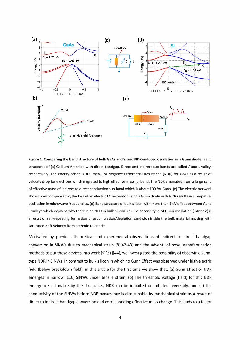
intense electric field. Figure 1.a shows the band structure of bulk GaAs in which the valley splitting or
offset between the energies of Γ and L valleys is about 300 meV. The Γ valley has a very low effective
mass (0.0632m0) where m0 is the free mass of electron. For low to moderate electric fields, most
3
electrons are within this sub band (valley) and contribute to large electron mobility (μH~ 8000 cm2/V.s)
[36]. As populating the L valley with high effective mass (0.55m0) occurs for higher electric fields (>
3000 V/cm) along the <111> crystallographic direction, the mobility, and as a result the current, reduce
(μL~ 2500 cm2/V.s) [See Figure 1.b]. This leads to an I-V characteristics or velocity versus electric field
as shown in Figure 1.c which has a NDR section. This mechanism of obtaining NDR in general was
proposed by Ridley [37] and Hlisum [38] and later as Ehrenreich experimentally obtained the band
structure of GaAs, the search for materials of suitable band structure for this type of NDR has begun
[39]. As the negative differential resistivity of the GaAs (or as it was later called Gunn diode) can
compensate the Ohmic loss in electric circuits, it was proposed to be applied in electric oscillators of
microwave frequencies (Figure 1.c).
However, the aforementioned electron transfer mechanism is lacking in bulk silicon, the reason of
which is evident by looking at its band structure in Figure 1.d. As it can be seen, the offset between X
and L sub bands is about 1 eV which mandates a very high voltage to induce NDR. Uniaxial straining of
p-type doped silicon was suggested to reduce this energy offset and initiate NDR [37]. Unaware of the
theoretical and experimental investigations of high electric field effect on charge transport in GaAs, J.
B. Gunn observed instabilities in the current flowing through a piece of GaAs under high voltage[40],
the source of which was the same I-V characteristics of Figure 1.c. He observed that when the electric
field reaches to a threshold value of 2000-4000 V/cm, the current (drift velocity) of electron drops and
an accumulation layer is built up after which there is a depleted region (positively charged) since the
electrons left that section with their high speed [See Figure 1.e].
The internal dipolar field of such accumulation/depletion sandwich reduces the total external field and
reverts the current back to its original value. After the dipolar region reaches to one end of the device,
i.e. moves from cathode and arrives at anode, the voltage across the device increases again, hence the
current increases to the point at which the same NDR drop occurs and the procedure repeats itself.
This results in an oscillating current around an average DC value [Figure 1.e]. This self-repeating
increase and decrease of current can reach up to 12 GHz in frequency depending on the length and
doping density. Length and drift velocity of electrons determine the transit time through the sample
or the frequency of current oscillation. Oscillations of the same origin were observed in materials like
CdTe, GaAs1-xPx, InP and GaSb [39]. In addition to exploiting this effect as an intrinsic source of
microwave oscillations, the resulting NDR in I-V characteristics, can also be used to compensate the
Ohmic loss of an electrical resonator (Figure 1.c). The oscillator of this type is called Gunn diode
oscillator and is used in microwave applications with frequencies of up to 100 GHz depending on the
required output power [41].
4
Figure 1. Comparing the band structure of bulk GaAs and Si and NDR-induced oscillation in a Gunn diode. Band
structures of (a) Gallium Arsenide with direct bandgap. Direct and indirect sub bands are called Γ and L valley,
respectively. The energy offset is 300 meV. (b) Negative Differential Resistance (NDR) for GaAs as a result of
velocity drop for electrons which migrated to high effective mass (L) band. The NDR emanated from a large ratio
of effective mass of indirect to direct conduction sub band which is about 100 for GaAs. (c) The electric network
shows how compensating the loss of an electric LC resonator using a Gunn diode with NDR results in a perpetual
oscillation in microwave frequencies. (d) Band structure of bulk silicon with more than 1 eV offset between Γ and
L valleys which explains why there is no NDR in bulk silicon. (e) The second type of Gunn oscillation (intrinsic) is
a result of self-repeating formation of accumulation/depletion sandwich inside the bulk material moving with
saturated drift velocity from cathode to anode.
Motivated by previous theoretical and experimental observations of indirect to direct bandgap
conversion in SiNWs due to mechanical strain [8][42-43] and the advent of novel nanofabrication
methods to put these devices into work [5][21][44], we investigated the possibility of observing Gunn-
type NDR in SiNWs. In contrast to bulk silicon in which no Gunn Effect was observed under high electric
field (below breakdown field), in this article for the first time we show that; (a) Gunn Effect or NDR
emerges in narrow [110] SiNWs under tensile strain, (b) The threshold voltage (field) for this NDR
emergence is tunable by the strain, i.e., NDR can be inhibited or initiated reversibly, and (c) the
conductivity of the SiNWs before NDR occurrence is also tunable by mechanical strain as a result of
direct to indirect bandgap conversion and corresponding effective mass change. This leads to a factor
5
of 2.3 change in the resistivity as the SiNW is strained between 0 % and -3 %. The NDR observed here
is different in essence from the NDR which arises in Esaki [45, 46] as well as Resonant Tunneling Diodes
(RTDs) [47, 48]. The abovementioned observations, i.e., (a), (b) and (c), promise application of SiNWs
in tunable microwave oscillators and mechanical (force, pressure) sensors. The rest of this article is
organized by explaining the computational methods including energy minimization, band structure,
and electron-phonon scattering rate calculations, followed by Ensemble Monte Carlo (EMC)
simulations. Thereafter, we will discuss the observed results and prospects of an experimental proof-
of-concept device.
METHODS
Energy Minimization and Band structure: Relaxation of the structural energy of SiNWs as well as
mechanical strain application are performed using Density Functional Theory (DFT) method as
implemented in SIESTA® [49]. The hydrogen terminated nanowires have [110] crystallographic
direction due to their proven relative stability compared to [100] direction [50]. To avoid the inherent
bandgap underestimation in DFT and diameter sensitive many–body GW corrections, the band
structure and eigenstates were calculated with 10 orbital (sp3d5s*) Tight Binding (TB) method using the
parameters given in reference [51]. The TB method has shown success in reproducing the experimental
data of the effect of radial strain on the photoluminescence spectra in narrow SiNWs [52, 53]. The
resulting unit cell after each minimization step is fed to the next minimization round by increasing or
decreasing the unit cell length (a) according to the desired strain amount (ε), i.e., ± aε as shown in
Figure 2.a. During these steps the volume of the unit cell is kept fixed in order to let the desired strain
take effect. A detailed EMC simulator was developed that incorporated the four lowest conduction sub
bands of the calculated band structure of SiNWs (strained & unstrained), to study the effect of
electron-phonon scattering under high electric fields.
Scattering Rates and Ensemble Monte Carlo (EMC) simulations: The electron-phonon scattering rates
were calculated with first order perturbation theory using Fermi’s Golden rule [54]. The total scattering
rate for a given state within a Brillouin Zone (BZ) with a wave vector of kz, is written as a sum over all
individual scattering rates from this state to available states kz’:
𝑊𝑘𝑧= ∑ 𝑊(𝑘𝑧, 𝑘𝑧
′ )𝑘𝑧′ . (1)
Here, W(kz, kz’) is the scattering rate of an electron from its initial state at kz to a possible final
(secondary) state (at kz’). W(kz, kz’) includes both inter- and intra-sub band electron-phonon scattering
events. The secondary (final) states corresponding to each initial state are determined by the phonon
type. For Longitudinal Acoustic (LA) phonons, all final states lie inside a window of Ez ± EDebye (starting
6
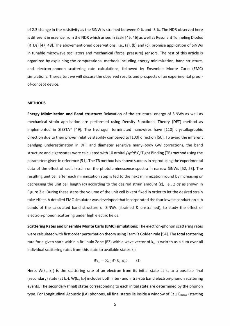
from initial state energy, Ez), and constitute all possible kz’. This is graphically shown in Figure 2.b for
an initial state in sub band 1 (B1), with all possible secondary states in sub band 3 (B3) marked by circles.
EDebye = 63 meV is the Debye energy or the maximum energy of LA phonons, and within the Debye
energy window (shaded strip on Figure 2.b), the secondary states form a quasi-continuum. In practice
however, the number of secondary states is limited by the resolution with which the BZ is discretized
along kz. For each individual term of equation (1) due to electron-LA phonon scattering, the
corresponding rate, i.e., W (kz, kz’), is written as follows:
𝑊(𝑘𝑧, 𝑘𝑧′ ) =
𝐷𝑒2
8𝜋2𝜌ℏ3𝑣𝑠4 ∆𝐸𝑘𝑘′
2𝐵± (|±∆𝐸
𝑘𝑘′
ℏ𝑣𝑠|) Φ(𝑞𝑡 , 𝑞𝑧). (2)
Here De, ρ and vs are electron deformation potential (De= 9.5 eV), mass density (ρ= 2329 Kg/m3) and
velocity of sound in silicon (vs=9.01×105 cm/s), respectively. 𝐵±(|�̃�|) is the Bose-Einstein factor of
phonons and it is 1 (𝑒ℏ𝜔𝑞
𝐾𝐵𝑇 − 1⁄ ) for absorption and 1 +1
(𝑒
ℏ𝜔𝑞𝐾𝐵𝑇−1)
for emission of a phonon, where ℏ𝜔𝒒
is the energy of a phonon with a wave vector of q. Ф is a structural factor involving inter-atomic and
intra-atomic matrix elements of terms like 𝑒−𝑖�̃�.(𝒓𝑚′−𝒓𝑚), where r is the coordinate of an atom. The
indices m and m’ are indices of different atoms within a unit cell. Details of deriving Ф is explained in
the Supplementary Information and reference [55]. ΔEkk’ is the energy difference between initial and
final states, and qt and qz are transverse and longitudinal wave vectors of phonons, respectively. When
electron scattering emanates from a Longitudinal Optical (LO) phonon, the secondary states are those
which lie exactly above or below the energy of the initial state (at kz) by ELO. Figure 2.c depicts an
example of finding available secondary states for an electron in B1 which is scattered to all other sub
bands including itself (intra-band scattering) assisted by LO phonons. As the optical phonon branch is
almost flat and independent of wave vector, then it is possible to assume a dispersion less or flat (i.e.,
kz independent) line on which all LO phonons have the same energy of ELO = 54 meV. The individual
rate in equation (1), W(kz, kz’), for LO phonons is then found by:
𝑊(𝑘𝑧, 𝑘𝑧′ ) =
|𝐷𝑜𝑝|2
8𝜋2𝜌𝜔0∫ Φ(𝑞𝑡, 𝑞𝑧)𝑑𝑞𝑡
𝑞𝑐
0𝐵±(𝐸𝐿𝑂 = ℏ𝜔0)
1
|𝜕𝐸(𝑘𝑧
,)
𝜕𝑞𝑧|𝑘𝑧
,=𝑘𝑝
, (3)
here Dop is deformation potential of LO phonons for electrons (Dop = 11×108 eV/cm), ωo is the maximum
phonon frequency of LO phonons or ELO/ħ, where ħ is Planck’s constant (ħ=6.582×10⁻¹⁶ eV.s), and qc is
the maximum allowable value of phonon transversal component (qt) within the BZ of bulk silicon which
is qc = 1.9π/a [56]. The last term in equation (3) is density of states evaluated at each available final
state (kp) into which an electron can scatter. The wave vectors of phonons and electrons are
represented by qz and kz, respectively. These quantities satisfy momentum conservation (See
7
Supplementary Information and reference [56]). The scattering rates as well as the corresponding final
states available after scattering are tabulated according to the index of the secondary sub band as well
as the type of scattering, i.e., phonon absorption (ABS) or phonon emission (EM) to be used by EMC
code. Figure 2.c shows a simple example of such table.
Within EMC simulation, a uniform electric field along the nanowire axis is applied, and temperature is
assumed to be uniform. Initially, electrons are assumed to be distributed uniformly with an equilibrium
thermal distribution. As time increase, the evolution of each electron under drift process with multi-
phonon scattering is recorded to calculate the electric current in response to the applied voltage (field).
At each step of EMC simulation [54], electron transport is confined to the first BZ, which is divided into
many kz grid points (e.g. 8001 points). Corresponding to each point, electron energy, scattering rates
and the available final states after scattering, are all recorded and fed into the EMC code from which
(a) the time dependent evolution of electron population at each state within the BZ as well as (b) the
velocity-electric field plots of the biased SiNWs, are obtained. Details of EMC can be found in reference
[57].
The methodology in this work was once used to predict population inversion in strained silicon
nanowires and modulation of electron-hole radiative recombination as a result of bandgap and wave
function symmetry change [42]. Modulation of recombination rates was later confirmed by
experimental works in reference [43]. Later theoretical works on SiGe nanowires also showed the
radiative life times of the same order of magnitude as our method [58], which supports the reliability
of our approach in predicting the carrier dynamics under the influence of electric field and multi-
phonon scattering events.
RESULTS & DISCUSSIONS
Figure 2.a illustrates the front view and side view of a 3.1 nm [110] unstrained silicon nanowire
terminated by hydrogen atoms. The top and bottom surfaces of the nanowire show canted silicon
dihydride (SiH2) units as a result of energy minimization in SIESTA®. The diameter is defined as the
average of long and short diameters. The band structure of the unstrained SiNW is shown in Figure 2.d
wherein the energy of electrons is plotted against the quasi momentum or wave vector along the
periodic length of the nanowire which is kz. The SiNW in this case shows a direct bandgap, i.e., both
minima of conduction and valence bands are at the same value of wave vector on BZ center or Γ point.
Four lowest conduction sub bands numbered from 1 to 4 [Figure 2.d] are those which are used in
calculation of electron-phonon scattering under high electric field. This is because the rest of the sub
bands are more than 5kBT ≈ 125 meV above the first sub band minimum and under moderate electric
fields they do not play any significant role in our study. The unstrained nanowire has a direct bandgap
8
of 1.554 eV at BZ center, and there are two indirect sub bands which lie symmetrically at kz = ±2.67/π
and their energy is 131 meV above the direct sub band minimum. We label this energy difference
between minima of direct and indirect conduction sub bands as energy offset ΔE as indicated in Figure
2.d.
Figure 2. Atomic structure of an unstrained 3.1 nm [110] SiNW and corresponding electronic (band) structure.
(a) Front view and side view of a 3.1nm [110] SiNW under no strain. Five unit cells of SiNW are shown in the side
view highlighting the canted SiH2 (silicon dihydride) units. (b) Graphical representation of finding secondary
states for an electron in sub band 1 (B1) which scatters to sub band 3 (B3) assisted by LA phonons. Ideally the
secondary states in B3 (shadowed strip) form a quasi-continuum. In simulation, this is limited by the resolution
of discretizing the BZ along kz. (c) The same graphical example for scattering from B1 to all sub bands (B1, B2, B3
and B4) assisted by LO phonons. Here there is a limited number of secondary states with corresponding rates
arranged in a table. (d) Band structure of the unstrained nanowire showing a direct bandgap value of Eg = 1.554
eV and an energy offset of ΔE = 131 meV. The first four conduction sub bands (numbered as S1, S2, S3 and S4)
are selected to calculate all electron-phonon scattering events required by EMC simulation.
It was previously observed that applying compressive strain lowers the indirect sub band energy and
shifts the direct conduction sub band as these bands are made of bonding and anti-bonding p orbitals,
respectively [42][9, 10]. Therefore, by continuing the application of compressive strain, there is a state
at which the direct and indirect sub bands change roles and the bandgap becomes indirect. Hence the
conduction sub band minimum and the valence sub band maximum are no longer at the same value
of wave vector. Here this transition or sub band flip point occurs at -2 % strain wherein the direct and
9
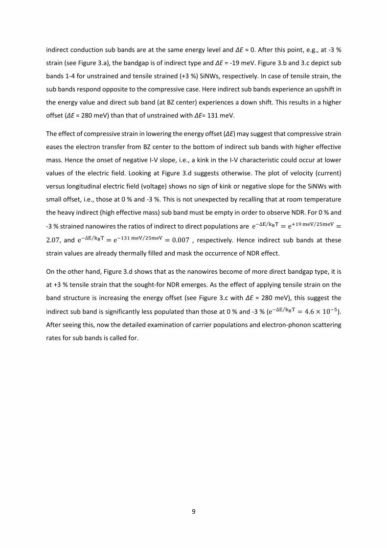
indirect conduction sub bands are at the same energy level and ΔE ≈ 0. After this point, e.g., at -3 %
strain (see Figure 3.a), the bandgap is of indirect type and ΔE = -19 meV. Figure 3.b and 3.c depict sub
bands 1-4 for unstrained and tensile strained (+3 %) SiNWs, respectively. In case of tensile strain, the
sub bands respond opposite to the compressive case. Here indirect sub bands experience an upshift in
the energy value and direct sub band (at BZ center) experiences a down shift. This results in a higher
offset (ΔE = 280 meV) than that of unstrained with ΔE= 131 meV.
The effect of compressive strain in lowering the energy offset (ΔE) may suggest that compressive strain
eases the electron transfer from BZ center to the bottom of indirect sub bands with higher effective
mass. Hence the onset of negative I-V slope, i.e., a kink in the I-V characteristic could occur at lower
values of the electric field. Looking at Figure 3.d suggests otherwise. The plot of velocity (current)
versus longitudinal electric field (voltage) shows no sign of kink or negative slope for the SiNWs with
small offset, i.e., those at 0 % and -3 %. This is not unexpected by recalling that at room temperature
the heavy indirect (high effective mass) sub band must be empty in order to observe NDR. For 0 % and
-3 % strained nanowires the ratios of indirect to direct populations are e−∆E kBT⁄ = e+19 meV 25meV⁄ =
2.07, and e−∆E kBT⁄ = e−131 meV 25meV⁄ = 0.007 , respectively. Hence indirect sub bands at these
strain values are already thermally filled and mask the occurrence of NDR effect.
On the other hand, Figure 3.d shows that as the nanowires become of more direct bandgap type, it is
at +3 % tensile strain that the sought-for NDR emerges. As the effect of applying tensile strain on the
band structure is increasing the energy offset (see Figure 3.c with ΔE = 280 meV), this suggest the
indirect sub band is significantly less populated than those at 0 % and -3 % (e−∆E kBT⁄ = 4.6 × 10⁻⁵).
After seeing this, now the detailed examination of carrier populations and electron-phonon scattering
rates for sub bands is called for.
10
Figure 3. Conduction sub bands and drift velocity of electrons in response to longitudinally applied electric
field under three strain values. (a) Four conduction sub bands of a -3 % strained 3.1nm [110] SiNW. The energy
offset in this case is ΔE=-19 meV, i.e., the bandgap is of indirect type. Panels (b) and (c) show the same sub bands
and their new energy values in response to 0 % and +3 % (tensile) strain, respectively. In these cases the offset
is ΔE= +131 meV and ΔE= +283 meV, respectively. (d) The drift velocity versus applied longitudinal electric field
is a plot proportional to current-voltage characteristics of the device (I-V). Application of tensile strain initiates
the current reduction or NDR at Ethreshold = 5x10⁵ V/m or 5000 V/cm.
By examining the carrier populations of each individual sub band (S1, S2, S3 and S4 Figure 4) we deduced:
For a -3 % strained nanowire (Figure 4.a), there is no pronounced increase of population in indirect sub
bands S3 and S4 (bottom panel) and the populations in sub bands S1 and S2 are changing in unison but
with different signs, i.e., as one of them is being filled (S1) the other one (S2) is being depleted. Hence
there is carrier transfer from sub band S1 to S2 via all inter-band events for which the scattering rate is
around 1 – 10 psec. In other words, both S1 and S2 are within the Debye energy window, facilitating
scattering between them rather than scattering (phonon absorption) to S3 and S4, which are at least
200 meV outside the Debye window.
11
Figure 4. Evolution of charge carrier (electron) population with electric field. Sub bands S1, S2, S3 and S4 are
shown by blue, red, green and black, respectively. Both in -3 % strained nanowire (a) and unstrained one (b), sub
band S2 is being emptied into indirect sub band S1, as the small offset value increases the chance of electron
scattering between S1 and S2. Hence there is no significant increase of population in sub bands S3 and S4 which
are very high above S1 and S2. For a +3 % strained SiNW (c), both sub bands S1 and S2 are being emptied and high
effective mass S4 is populated significantly.
Observing the same behavior as that of Figure 4.a for carrier populations of unstrained nanowire
(Figure 4.b), confirms this interpretation. For unstrained SiNW, the indirect sub band S1 and S2 are again
being emptied in favor of filling up direct sub band S1 as the distance from indirect (S1 & S2) minima to
indirect (S3 & S4) minima is about 200 meV which makes the phonon absorption events to S3 and S4
less probable.
Consequently for -3 % and 0 % strained SiNWs no NDR is observed. However recalling Figure 3.d, and
comparing I-V plots for the two cases (blue and red) suggests that indirect bandgap nanowires (i.e. -3
12
% strained) have higher resistivity than unstrained SiNW by a factor of 2.3. This is because the indirect
sub bands of -3 % SiNW are responsible for charge transport and as their effective mass is four times
larger than the direct sub band, less mobility or conductivity is expected. Biasing a nanowire with a
fixed bias voltage and switching the nanowire between unstrained and compressively strained states
will result in a strain sensitive resistor or mechanical force sensor.
Further examination of Figure 3.d reveals that the peak in the velocity-field plot, is shifting to lower
electric field values as strain is relaxed from -3 % to 0 %. Finally, at +3 % strain where the offset is
maximal, (ΔE = 280 meV), NDR emerges. This is because after the carriers scatter into indirect sub
bands (direct S1 & S2 indirect S1 & S2), they now have a higher probability to scatter into indirect sub
bands S3 and S4 which are now closer as opposed to the rest of sub bands i.e. direct S1 & S2, and direct
S3 & S4 (See Figure 4.c). The significant increase in population in indirect S3 and S4 (bottom of panel of
Figure 4.c) confirms that both S1 and S2 are being emptied (top panel) in favor of transferring carriers
to high effective mass indirect S3 and S4 which results in current drop and NDR (see Figure 3.d). Seeing
this suggests that increasing the energy offset between direct and indirect sub band leads to reduced
backscattering probability for those electrons which travelled to indirect sub bands S1 and S2.
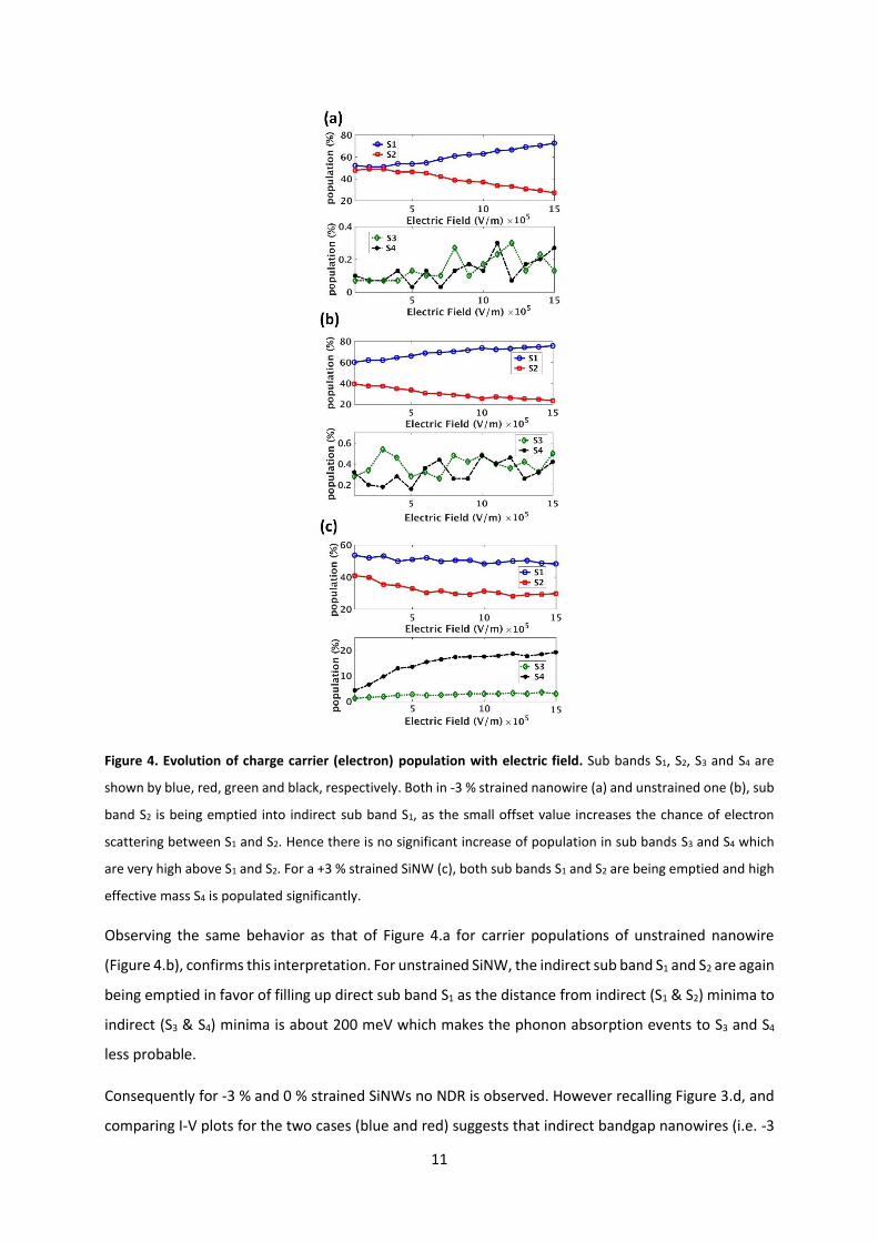
Hence they will find have a higher probability to absorb phonons and end up being in indirect S3 and
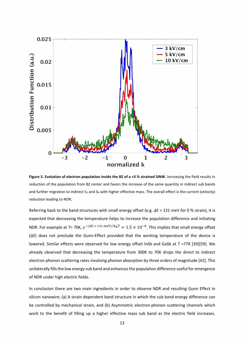
S4 which are of higher effective mass. Figure 5 shows the evolution of electron population within the
BZ of +3 % strained SiNW. It reveals how the population decays from direct sub bands (around BZ
center) by increasing the electric field and migrates to indirect ones with higher effective mass which
leads to lower velocity.
13
Figure 5. Evolution of electron population inside the BZ of a +3 % strained SiNW. Increasing the field results in
reduction of the population from BZ center and favors the increase of the same quantity in indirect sub bands
and further migration to indirect S3 and S4 with higher effective mass. The overall effect is the current (velocity)
reduction leading to NDR.
Referring back to the band structures with small energy offset (e.g. ΔE = 131 meV for 0 % strain), it is
expected that decreasing the temperature helps to increase the population difference and initiating
NDR. For example at T= 70K, 𝑒−(∆E = 131 meV) kBT⁄ = 1.5 × 10⁻⁸. This implies that small energy offset
(ΔE) does not preclude the Gunn-Effect provided that the working temperature of the device is
lowered. Similar effects were observed for low energy offset InSb and GaSb at T =77K [39][59]. We
already observed that decreasing the temperature from 300K to 70K drops the direct to indirect
electron-phonon scattering rates involving phonon absorption by three orders of magnitude [42]. This
unilaterally fills the low energy sub band and enhances the population difference useful for emergence
of NDR under high electric fields.
In conclusion there are two main ingredients in order to observe NDR and resulting Gunn Effect in
silicon nanowire; (a) A strain dependent band structure in which the sub band energy difference can
be controlled by mechanical strain, and (b) Asymmetric electron-phonon scattering channels which
work to the benefit of filling up a higher effective mass sub band as the electric field increases.
14
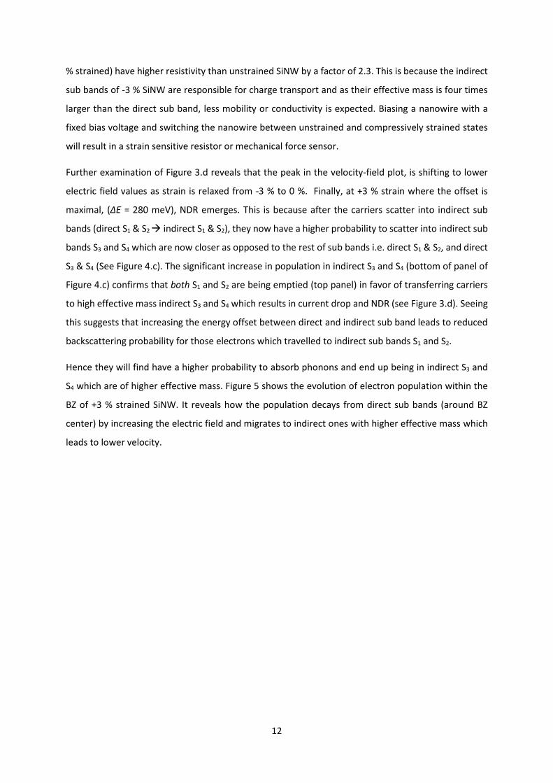
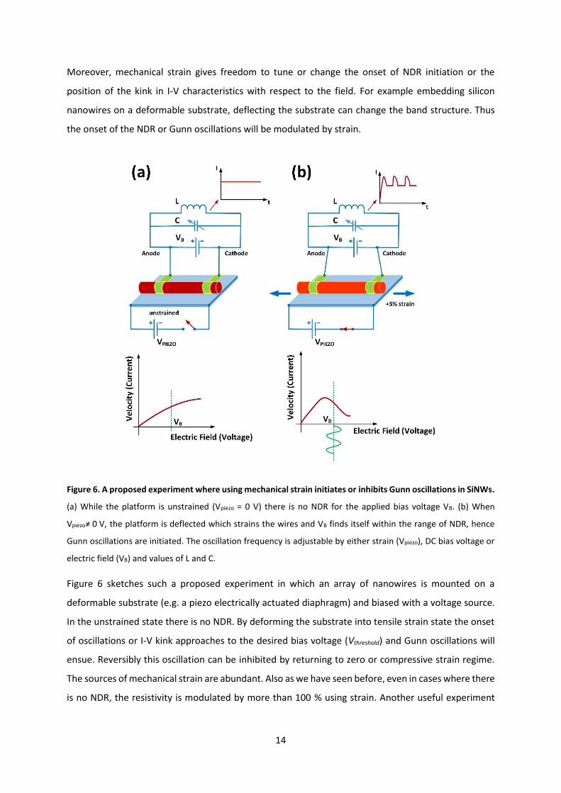
Moreover, mechanical strain gives freedom to tune or change the onset of NDR initiation or the
position of the kink in I-V characteristics with respect to the field. For example embedding silicon
nanowires on a deformable substrate, deflecting the substrate can change the band structure. Thus
the onset of the NDR or Gunn oscillations will be modulated by strain.
Figure 6. A proposed experiment where using mechanical strain initiates or inhibits Gunn oscillations in SiNWs.
(a) While the platform is unstrained (Vpiezo = 0 V) there is no NDR for the applied bias voltage VB. (b) When
Vpiezo≠ 0 V, the platform is deflected which strains the wires and VB finds itself within the range of NDR, hence
Gunn oscillations are initiated. The oscillation frequency is adjustable by either strain (Vpiezo), DC bias voltage or
electric field (VB) and values of L and C.
Figure 6 sketches such a proposed experiment in which an array of nanowires is mounted on a
deformable substrate (e.g. a piezo electrically actuated diaphragm) and biased with a voltage source.
In the unstrained state there is no NDR. By deforming the substrate into tensile strain state the onset
of oscillations or I-V kink approaches to the desired bias voltage (Vthreshold) and Gunn oscillations will
ensue. Reversibly this oscillation can be inhibited by returning to zero or compressive strain regime.
The sources of mechanical strain are abundant. Also as we have seen before, even in cases where there
is no NDR, the resistivity is modulated by more than 100 % using strain. Another useful experiment
15
could be bending and unbending a long nanowire similar to those fabricated by [43][60], and recording
the voltage across the bent sections which are under tensile strain.
Adding spin degree of freedom to this effect will also lead to a rich playground for
physical effects and promising spintronic devices [61, 62]. We speculate that in nanowires with large
Spin Orbit Interaction (SOI) e.g. InSb, the combination of electric field and mechanical strain will lead
to interesting spin-resolved Gunn Effect or oscillations of spin up or spin down currents as they can be
initiated under different voltages and strain values (spin resolved Gunn Effect). Alloying SiNWs with
germanium is another way of tailoring the band structure and threshold voltage for NDR initiation. The
recent techniques of growing SiGe nanowires e.g. in core-shell form are promising [44]. In addition, it
was experimentally observed [63] that applying perpendicular magnetic field on bulk InSb samples
reduces the Gunn Effect threshold voltage due to Hall Effect. Adding this degree of freedom to the
presented theoretical models uncovers new phenomena worth of understanding and consummating
to device applications.
In summary using DFT, TB and ensemble Monte Carlo simulations we observed that; firstly, in contrast
to bulk silicon, Gunn Effect is observable in [110] SiNWs under tensile strain of 3 %. This is the result a
tunable direct bandgap with high energy offset (ΔE) which creates the same mechanism occurring in
GaAs, i.e., migration of electrons from low effective mass sub band to indirect high effective mass one
as a result of which NDR emerges. Secondly, the value of threshold field to induce Gun Effect reversible
adjustable by mechanical strain. Thirdly, direct to indirect bandgap conversion in response to the
applied strain causes more than 100 % change of resistivity. All the above mentioned observations are
promising for more applications of silicon nanowires in the realm of electronic and nano-mechanical
devices.
ACKNOWLEDGEMENTS:
D.S acknowledges access to the supercomputing facilities provided by Shared Hierarchical Academic
Research Computing Network (SHARCNET®) in Ontario, Canada while he was working at University of
Waterloo. A.I and D.S acknowledge financial support from Swedish Research Council
(Vetenskapsrådet). M.P.A was supported by the National Science Foundation through the Division of
Electrical, Communications and Cyber Systems under Grant ECCS-1231927. A.V and R.N acknowledge
access to supercomputing facilities of Texas Advanced Computing Center (TACC).
16
REFERENCES:
[1] International Technology Roadmap for Semiconductors (ITRS) report 2015, http://www.itrs2.net/
[2] Fangxia Shen, Jindong Wang, Zhenqiang Xu, Yan Wu, Qi Chen, Xiaoguang Li, Xu Jie, Lidong Li, Maosheng Yao,
Xuefeng Guo, and Tong Zhu, Rapid Flu Diagnosis Using Silicon Nanowire Sensor, Nano Lett., 12(7), 3722–3730
(2012).
[3] S. Hashimoto and S. Asada and T. Xu and S. Oba and Y. Himeda and R. Yamato and T. Matsukawa and T.
Matsuki and T. Watanabe, Anomalous Seebeck coefficient observed in silicon nanowire microthermoelectric
generator, Appl. Phys. Lett. 111, 023105 (2017).
[4] Daniel Ramos, Eduardo Gil-Santos, Oscar Malvar, Jose M. Llorens, Valerio Pini, Alvaro San Paulo, Montserrat
Calleja, and Javier Tamayo, Silicon nanowires: where mechanics and optics meet at the nanoscale, Scientific
Reports 3, 3445 (2013).
[5] A. Lugstein, M. Steinmair, A. Steiger, H. Kosina and E. Bertagnolli, Anomalous Piezoresistance Effect in
Ultrastrained Silicon Nanowiresm, Nano Lett., 2010, 10 (8), pp 3204–3208.
[6] Ruiyuan Liu, Jie Wang, Teng Sun, Mingjun Wang, Changsheng Wu, Haiyang Zou, Tao Song, Xiaohong Zhang,
Shuit-Tong Lee, Zhong Lin Wang , and Baoquan Sun, Silicon Nanowire/Polymer Hybrid Solar Cell-Supercapacitor:
A Self-Charging Power Unit with a Total Efficiency of 10.5%, Nano Lett., 17(7), pp 4240–4247, (2017).
[7] X. Zianni and A. G. Nassiopoulou, Photoluminescence lifetimes of Si quantum wires, Phys. Rev. B 66, 205323
(2002)
[8] D. Shiri, Y. Kong, A. K. Buin, and M. P. Anantram, Strain induced change of bandgap and effective mass in
silicon nanowires, Appl. Phys. Lett. 93, 073114, (2008).
[9] K. -H. Hong, J. Kim, S. -H. Lee and J. K. Shin, Strain-driven electronic band structure modulation of Si nanowires,
Nano Lett. 8(5), 1335 (2008).
[10] P. W. Leu, A. Svizhenko, and K. Cho, Ab initio calculations of the mechanical and electronic properties of
strained Si nanowires, Phys. Rev. B 77, 235305 (2008).
[11] Z. Wu, J. B. Neaton, and C. Grossman, Charge separation via strain in silicon nanowires, Nano Lett. 9(6), 2418
(2009).
[12] Y. Ahn, J. Dunning, and J. Park, Scanning photocurrent imaging and electronic band studies in silicon
nanowire field effect transistors, Nano Lett. 5(7), 1367 (2005).
[13] C. Yang, C. J. Barrelet, F. Capasso, and C. M. Lieber, Single p-type/Intrinsic/n-type silicon nanowires as
nanoscale avalanche photo detectors, Nano Lett. 6(12), 2929 (2006).
[14] O. Hayden, R. Agarwal, and C. M. Lieber, Nanoscale avalanche photodiodes for highly sensitive and spatially
resolved photon detection, Nature Materials 5, 352 (2006).
[15] A. Zhang, S. You, C. Soci, D. Wang, and Y.-H. Lo, in Planar and Vertical Si Nanowire Photo Detectors, Lasers
and Electro-Optics, and Conference on Quantum Electronics and Laser Science, CLEO/QELS, San Jose, California,
USA (2008).
[16] M. J. Lo Fro, et al., Light Emission form fractal array of silicon nanowires, EMRS-2017 Spring Meeting, May
22-26, 2017, Strasbourg, France.
[17] R. S. Jacobsen et al., Strained silicon as a new electro-optic material, Nature 441, 199 (2006).
[18] B. Chmielak, M. Waldow, C. Matheisen, C. Ripperda, J. Bolten, T. Wahlbrink, M. Nagel, F. Merget, and H.
Kurz, Pockels effect based fully integrated, strained silicon electro-optic modulator, Optics Express Vol. 19, Issue
18, pp. 17212-17219 (2011).
[19] M. Cazzanelli et al., Second-harmonic generation in silicon waveguides strained by silicon nitride, Nature
Materials 11, 148 (2011).
[20] Daryoush Shiri, Ab initio Study of Nonlinear Optical Susceptibilities in Silicon Nanowires, arXiv: 1707.08324
[cond-mat.mes-hall]
[21] K. E. Moselund et al., Bended gate-all-around nanowire mosfet: A device with enhanced carrier mobility due
to oxidation-induced stress, in IEDM Digest of Technical Papers (IEDM, 2007).
[22] V. Pott et al., Fabrication and characterization of gate-all-around silicon nanowires on bulk silicon, IEEE Trans.
Nanotechnol. 7(6), 733 (2008).
17
[23] S. De Franceschi; R. Maurand; A. Corna; D. Kotekar-Patil; X. Jehl; M. Sanquer; R. Lavieville; L. Hutin; S.
Barraud; M. Vinet; Y. -M. Niquet, SOI platform for spin qubits, 2016 Joint International EUROSOI Workshop and
International Conference on Ultimate Integration on Silicon (EUROSOI-ULIS), 25-27 Jan. 2016, pages 124-126,
2016.
[24] Y. Hu, F. Kuemmeth, C. M. Lieber, and C. M. Marcus, Hole spin relaxation in Ge-Si core-shell nanowire qubits,
Nature Nanotechnology 7, 47 (2012).
[25] A. P. Higginbotham, T. W. Larsen, J. Yao, H. Yan, C. M. Lieber, C. M. Marcus, and F. Kuemmeth, Hole Spin
Coherence in a Ge/Si Heterostructure Nanowire, Nano Lett., 14 (6), pp 3582–3586, (2014).
[26] B. Voisin, R. Maurand, S. Barraud, M. Vinet, X. Jehl, M. Sanquer, J. Renard, S. De Franceschi, Electrical control
of g-factors in a few-hole silicon nanowire MOSFET, Nano Lett. 16, 88 (2016).
[27] Krutarth Trivedi, Hyungsang Yuk, Herman Carlo Floresca, Moon J. Kim, and Walter Hu, Quantum
Confinement Induced Performance Enhancement in Sub-5-nm Lithographic Si Nanowire Transistors, Nano Lett.,
11(4), pp 1412–1417, (2011).
[28] André Heinzig, Stefan Slesazeck, Franz Kreup, Thomas Mikolajick, and Walter M. Weber, Reconfigurable
Silicon Nanowire Transistors, Nano Lett., 12(1), pp 119–124, (2012).
[29] Muhammad M. Mirza, Felix J. Schupp, Jan A. Mol, Donald A. MacLaren, G. Andrew D. Briggs, and Douglas J.
Paul, One dimensional transport in silicon nanowire junction-less field effect transistors, Scientific Reports 7,
3004 (2017).
[30] Wooyoung Shim, Jun Yao, and Charles M. Lieber, Programmable Resistive-Switch Nanowire Transistor Logic
Circuits, Nano Lett., 2014, 14(9), pp 5430–5436.
[31] Q. Li et al., Silicon nanowire on oxide/nitride/oxide for memory application, Nanotechnol. 18, 235204 (2007).
[32] D. Sacchetto, M. H. Ben-Jamaa, S. Carrara, G. De Micheli, and Y. Leblebici, Memristive devices fabricated
with silicon nanowire schottky barrier transistors, Circuits and Systems (ISCAS), Proceedings of 2010 IEEE
International Symposium on, 30 May-2 June 2010, pages 9-12.
[33] Joshua Yang, Dmitri B. Strukov, and Duncan R. Stewart, Memristive devices for computing, Nature
Nanotechnology, 8, 13-24 (2013).
[34] Francesco Priolo, Tom Gregorkiewicz, Matteo Galli, and Thomas F. Krauss, Silicon nanostructures for
photonics and photovoltaics, Nature Nanotechnology 9, 19–32 (2014).
[35] J. Ramanujam, D. Shiri, and A. Verma, Silicon Nanowire Growth and Properties: A Review, Mater. Express
1(2), 105–126 (2011).
[36] J. S. Blakemore, Semiconducting and other major properties of gallium arsenide, Journal of Applied Physics
53, R123 (1982).
[37] B. K. Ridley, and T. B. Watkins, Proc. Phys. Soc. 78, 293 (1961).
[38] C. Hilsum, Proc. IRE, 50, 185 (1962).
[39] Esther M. Conwell, High Field Transport in Semiconductors, Solid State Physics, Supplement 9, Academic
Press, NY 1967.
[40] J. B. Gunn, Microwave oscillations of current in III–V semiconductors, Solid State Commun. 1, 88 (1963).
[41] Robert E. Collin, Foundations of Microwave Engineering, McGraw-Hill, New York 1991.
[42] D. Shiri, A. Verma, C. R. Selvakumar, and M. P. Anantram, Reversible Modulation of Spontaneous Emission
by Strain in Silicon Nanowires, Scientific Reports 2, 461; DOI: 10.1038/srep00461 (2012).
[43] E. M. Grumstrup, M. M. Gabriel, C. W. Pinion, J. K. Parker, J. F. Cahoon , and J. M. Papanikolas , Reversible
strain-induced electron–hole recombination in silicon nanowires observed with femto second pump–probe
microscopy, Nano Lett. 14(11), 6287–6292 (2014).
[44] D. C. Dillen, F. Wen , K. Kim , and E. Tutuc , Coherently Strained Si–SixGe1–x Core–Shell Nanowire
Heterostructures, Nano Lett. 16(1), 392 (2016).
[45] L. Esaki, New Phenomenon in Narrow Germanium p−n Junctions, Phys. Rev. 109, 603 (1958).
[46] Heinz Schmid, Cedric Bessire, Mikael T. Björk, Andreas Schenk, and Heike Riel, Silicon Nanowire Esaki Diodes,
Nano Lett., 2012, 12(2), pp 699–703.
[47] T. C. L. G. Sollner, W. D. Goodhue, P. E. Tannenwald, C. D. Parker, D. D. Peck: Resonant tunneling through
quantum well at frequencies up to 2.5 THz. Appl. Phys. Lett. 43, 588–590 (1983)
18
[48] Peter Y. Yu, and Manuel Cardona, Fundamentals of Semiconductors: Physics and Materials Properties, 4th
Edition, Springer-Verlag Berlin Heidelberg 2010.
[49] J. M. Soler, et al., The SIESTA method for ab initio order-N materials simulation, J. Phys.: Condens. Matter.
14, 2745 (2002).
[50] D. D. D. Ma , C. S. Lee , F. C. K. Au , S. Y. Tong , and S. T. Lee , Small-diameter silicon nanowire surfaces,
Science 299, 1874 (2003).
[51] J.-M. Jancu, R. Scholz, F. Beltram, and F. Bassani, Empirical sp3d5s∗ tight-binding calculation for cubic
semiconductors: General method and material parameters, Phys. Rev. B, Condens. Matter Mater. Phys., vol. 57,
no. 11, pp. 6493–6507, Mar. 1998.
[52] S. S. Walavalkar, C. E. Hofmann, A. P. Homyk, M. D. Henry, H. A. Atwater, and A. Scherer, Tunable visible and
near-IR emission from sub-10 nm etched single-crystal Si nanopillars, Nano Lett. 10(11), 4423 (2010).
[53] O. Demichel, et al., Quantum confinement effects and strain-induced band-gap energy shifts in core-shell Si-
SiO2 nanowires, Phys. Rev. B. 83, 245443 (2011).
[54] K. Tomizawa, Numerical Simulation of Submicron Semiconductor Devices (Artech House, Boston, London,
1993).
[55] D. Shiri, see http://hdl.handle.net/10012/7097 for Electronic and Optical Properties of Silicon Nanowires:
Theory and Modeling, UWSpace, 2012.
[56] A. K. Buin, A. Verma, and M. P. Anantram, Carrier-phonon interaction in small cross-sectional silicon
nanowires, J. Appl. Phys. 104, 053716 (2008).
[57] A. Verma, A. K. Buin, and M. P. Anantram, High-field hole transport in silicon nanowires, J. Appl. Phys. 106,
113713 (2009).
[58] X. Cartoixà, M. Palummo, H. Ikaros, T. Hauge, Erik P. A. M. Bakkers, and Riccardo Rurali, Optical Emission in
Hexagonal SiGe Nanowires, Nano Lett.,17(8),4753–4758 (2017).
[59] John E. Smith Jr., Marshall I. Nathan, James C. McGroddy, Sylwester A. Porowski, and William Paul, GUNN
EFFECT in n‐TYPE InSb, Appl. Phys. Lett. 15, 242 (1969).
[60] S. Y. Ryu, et al, Lateral buckling mechanics in silicon nanowires on elastomeric substrates, Nano Lett. 9, 3214
(2009).
[61] Qi, Y., Yu, Z-G. & Flatte, M. E. Spin Gunn Effect. Phys. Rev. Lett. 96, 026602 (2006).
[62] N. Okamoto, H. Kurebayashi, T. Trypiniotis, I. Farrer, D. A. Ritchie, E. Saitoh, J. Sinova, J. Mašek, T. Jungwirth
and C. H. W. Barnes, Electric control of the spin Hall effect by intervalley transitions, Nature Materials 13, 932–
937 (2014).
[63] H. Heinrich, and W. Keeler, Gunn effect threshold and domain formation in transverse magnetic fields in
indium antimonide, Appl. Phys. Lett., 21, 171 (1972).