defect studies of znse nanowires
TRANSCRIPT
IOP PUBLISHING NANOTECHNOLOGY
Nanotechnology 19 (2008) 215715 (6pp) doi:10.1088/0957-4484/19/21/215715
Defect studies of ZnSe nanowiresU Philipose1, Ankur Saxena1, Harry E Ruda1, P J Simpson2,Y Q Wang3 and K L Kavanagh3
1 Centre for Nanotechnology, University of Toronto, 170 College Street, Toronto,ON, M5S 3E4, Canada2 Department of Physics and Astronomy, University of Western Ontario, London,ON, N6A 3K7, Canada3 Department of Physics, Simon Fraser University, Burnaby, BC, V5A 1S6, Canada
Received 21 November 2007Published 23 April 2008Online at stacks.iop.org/Nano/19/215715
AbstractDuring the synthesis of ZnSe nanowires various point and extended defects can form, leading toobserved stacking faults and twinning defects, and strong defect related emission inphotoluminescence spectra. In this paper, we report on the development of a simplethermodynamic model for estimating the defect concentration in ZnSe nanowires grown undervarying Se vapour pressure and for explaining the results of our experimental findings. Positronannihilation spectroscopy was used successfully for the first time for nanowires and the resultssupport predictions from the defect model as well as agreeing well with our structural andoptical characterization results. Under very high Se vapour pressure, Se nodules were observedto form on the sidewalls of the nanowire, indicating that beyond a limit, excess Se will begin toprecipitate out of the liquid alloy droplet in the vapour–liquid–solid growth of nanowires.
1. Introduction
ZnSe is an important material for fabrication of optoelectronicdevices on account of its direct and wide bandgap. Therehas been considerable effort expended toward developing ZnSenanostructures since control of size and dimensions can lead tounique optical and electronic properties. These direct band gapnanostructures should be characterized by high near bandgapluminescence, but this is not often the case. Even in bulk ZnSe,despite decades of research, emission is often dominated bylow energy luminescence bands caused by point defects whichintroduce energy levels within the bandgap of ZnSe [1, 2].This is the main problem impeding the development of twodimensional (2D) ZnSe based laser devices: a high defectdensity causing generation and propagation of non-radiativerecombination defects (dark line defects) [3]. However,as dimensions are further reduced, one dimensional ZnSestructures show properties quite different from that of 2Dstructures or bulk materials because of strain relaxation effects.In nanowires with small diameters and large surface area, straincan be easily accommodated, thus inhibiting the formationof misfit dislocations and dark line defects. Another areaof difference between bulk ZnSe and ZnSe nanowires hasbeen the dependence of defect density on growth conditions.In [4], it was shown that ZnSe epitaxial films grown bymolecular beam epitaxy (MBE) under Se overpressure leadsto a low defect material when compared with those grown
under Zn overpressure. This is on contrast to our findingswith ZnSe nanowires grown by VLS at 650 ◦C [5]. Weobserve a reduction in the defect density for nanowires grownunder Zn-rich conditions as compared to those grown underSe-rich conditions and our results agrees well with work onZnSe epitaxial films grown by metal organic vapour phaseepitaxy [6] and works on MBE [7]. It is not clear at this stageif the reason for this difference in the structural and opticalquality of ZnSe can be attributed to a difference in the growthconditions or mechanism. We believe that the growth of thenanowire and the occurrence of native defects are influencednot just by the growth kinetics but also by its thermodynamics.Hence, there is a need to develop a thermodynamic modelwhich would qualitatively explain our experimental findings.
In an attempt to synthesize crystalline ZnSe nanowireswith good structural and optical quality, several researchgroups have reported success. But, the focus of these studieshas been on synthesis and structural characterization [8, 9].Studies on photoluminescence measurements report thepresence of low energy luminescence bands in unintentionallydoped ZnSe nanowires [11–13], which is evidence of intrinsicpoint defects of the ZnSe lattice. However, no detailed studytracing the origin of these defects to growth conditions noran estimate of the defect concentration in these nanowires hasbeen reported. Hence, a detailed knowledge of the formationand nature of these defects is mandatory in order to developthese nanostructures for device applications.
0957-4484/08/215715+06$30.00 © 2008 IOP Publishing Ltd Printed in the UK1

Nanotechnology 19 (2008) 215715 U Philipose et al
In binary compounds like ZnSe, various forms of intrinsicpoint defects may occur, having appropriate positive ornegative charges. The principle defects include vacancies onthe sublattice of Zn (Vx
Zn) and Se (VxSe), interstitial atoms
(IZn) and (ISe), antistructural defects (SeZn) and (ZnSe) (Seatom in the Zn sublattice and vice versa) and positively andnegatively single- and double-charged vacancies (V+
Se, V2+Se ,
V−Zn and V2−
Zn ). There is no experimental evidence of antisitedefects in ZnSe [14] and hence these defects are not consideredhenceforth. The native defects in ZnSe nanowires consideredin this work, based on the optical characterization and post-growth annealing treatment results of [5], are the vacancyand interstitial defects and hence this work takes into accountthe neutral, the singly and doubly charged Zn vacancies andinterstitials [14–16]. The neutral Zn vacancy has a threefold-degenerate level in the band gap and the possible charged statesare 1− and 2−, corresponding to the Zn vacancy levels actingas acceptor levels in undoped ZnSe. Similarly, the neutralZn interstitial has two electrons occupying a single level inthe bandgap and the possible charge states are 1+ and 2+,and their levels act as donor states in the bandgap of undopedZnSe [14]. The vacancies and interstitials of Zn havingdifferent charge states create different localized levels withinthe band gap and can also combine to form donor–acceptorpairs (DAP). Evidence of the existence of such DAPs has alsobeen confirmed by photoluminescence (PL) measurements,discussed in greater detail in [17].
The approach of this work is to review the thermodynam-ics of intrinsic defects in ZnSe, develop a model showing thedependence of the point defects on growth parameters, as wellas provide experimental evidence of their existence using pho-toluminescence (PL) and positron annihilation spectroscopy(PAS). PAS is an important technique that can provide informa-tion on the relative vacancy concentration. Positrons trappedat vacancy defects (trapped due to reduced nuclear density atvacancies) tend to annihilate with the slower moving valenceelectrons, which will give rise to a narrower momentum dis-tribution and hence an increase in the S-parameter [18]. TheS-parameter thus tends to be higher for a sample with a highconcentration of defects than for defect free samples, due to re-duced annihilation with high momentum core electrons. Trap-ping is possible only at neutral or negatively charged vacancies,since Coulomb repulsion prevents the trapping of positrons atpositively charged vacancies. Se vacancies, which are dou-bly ionized donor centres, are expected to be effective positrontraps in the neutral state but not when they are ionized, i.e. pos-itively charged with regard to the lattice. On the other hand, Znvacancies act as acceptor centres and therefore can be effectivepositron traps when ionized. The same is true for any Zn va-cancy related acceptor centre. Hence, we can conclude thatany change in the S-parameter during the PAS measurementsis due to a change in the Zn vacancy related defects and sincethe dominant Zn vacancies are the doubly charged Zn vacan-cies, (V2−
Zn ), we can safely assume that the S-parameter gives ameasure of [V2−
Zn ].
Table 1. Equilibrium constants derived from reaction equations.
Reaction equations leadingto the formation ofvacancies and interstitials
Equations for equilibriumconstants based onmass-action relation
Zn(v) + 12 (Se2)(v) = ZnSe(s) Kf = PZn P1/2
Se2
12 (Se2)(v) = Sex
Se + V2−Zn + 2ho Kv = [V2−
Zn ]p2
P1/2Se2
V2−Zn + ho = V−
Zn K′Zn = [V−
Zn][V2−
Zn ]p
V−Zn + ho = Vx
Zn K xZn = [Vx
Zn][V−
Zn]p
V2−Zn + I2+
Zn = 0 K f r = [V2−Zn ][I2+
Zn ]I2+
Zn + e− = I+Zn K +i = [I+Zn]
[I2+Zn ]n
I+Zn + e− = IxZn K x
i = [IxZn]
[I+Zn]n
2. Model
A vapour–liquid–solid mechanism accounts for the formationof ZnSe nanowires and their formation follows the reaction:
ZnSe(s) = Zn(v) + 12 Se2(v). (1)
The nanowire growth is driven by the chemical potentialgradients between vapour, liquid and solid phase with growthtaking place through a mass transfer across the liquid–solidinterface. The system of nanowires is characterized by atemperature T , at which there are a certain number of intrinsicpoint defects in the crystalline nanowires. The concentrationof Zn vacancies and interstitials, [VZn] and [IZn], respectively,were estimated from [14, 19]:
[V] = Nsites Nconfig exp
(S
k
)exp
(− Ef
kT
)(2)
where, S is the entropy, Ef is the formation energy of thedefect, Nsites is the number of sites in the lattice (per unitvolume) where the defect can be incorporated (i.e., for ZnSe,Nsites = 2.2 × 1022 cm−3), k is Boltzmann’s constant, T is theabsolute temperature and Nconfig is the number of equivalentconfigurations in which the defect can be incorporated. Forvacancy defects [20], Nconfig = 1. The entropy and theformation energy of a given defect were estimated basedon the experimental data of [17]. The vacancy formationreactions and the corresponding mass-action relations are givenin table 1. The concentrations of free electrons and holes areindicated by p and n and in reaction equations, free electronsand holes are indicated by e− and ho, respectively.
For the assumptions discussed above, the electricalneutrality condition reduces to [21]:
n + 2[V2−Zn ] + [V−
Zn] = p + 2[I2+Zn ] + [I+Zn]. (3)
The Zn partial pressure (PZn) and Se2 partial pressure (P1/2Se2
)
in the vapour phase are governed by the equation:
PZn P1/2Se2
= Kf (4)
2

Nanotechnology 19 (2008) 215715 U Philipose et al
Figure 1. Evolution chart of defects, where arrows refer toincreasing (P1/2
Se2).
Table 2. Approximate electron neutrality conditions.
n = p 2[V2−Zn ] = p [V−
Zn] = p
n = 2[I2+Zn ] 2[V2−
Zn ] = 2[I2+Zn ] [V−
Zn] = 2[I2+Zn ]
n = [I+Zn] 2[V2−Zn ] = [I+Zn] [V−
Zn] = [I+Zn]
where Kf (in units of (atm)3/2) is the equilibrium constant forsublimation of ZnSe, which is a constant at a given temperatureand is given by the equation [22]:
log Kf = −17 818
T+ 9.1888. (5)
During growth, the compound ZnSe source provided aminimum total pressure Pmin over the growing nanowire inthe growth chamber, ensuring that it remained an equilibriumZnSe solid phase. The required minimum partial pressure ofSe, (P1/2
Se2)min was calculated using the approximation:
(P1/2Se2
)min ≈ (Kf/2)1/3. (6)
At a growth temperature of 650 ◦C (923 K), (P1/2Se2
)min is3.4 × 10−4 atm (equations (5) and (6)).
To calculate the concentration of the six defects ([V2−Zn ],
[V−Zn], [Vx
Zn], [I+Zn], [I2+Zn ] and [Ix
Zn]), as a function of (P1/2Se2
),equations in table 1 were modified and expressed in terms ofthe equilibrium constants. Based on the electrical neutralityconditions of equation (3), a set of nine approximate electricalneutrality conditions were established and are shown intable 2. Based on these nine electrical neutrality conditions,the evolution chart of the defects and the possible transitionswith increasing Se vapour pressure (P1/2
Se2) is shown in
figure 1. The dependence of [VZn] and [IZn] equilibriumconcentrations on (P1/2
Se2) was established using the mass-action
laws and the charge neutrality conditions [23]. Figure 2shows the approximate solution of this set of equations. Theapproximation implies that in the ranges of (P1/2
Se2) pressure
variation, three defect regimes (2[I2+Zn ] = 2[V2−
Zn ], p =2[V2−
Zn ], and p = [V−Zn]) of the nine regimes shown in
figure 1 are considered. At low values of (P1/2Se2
), the
approximation 2[I2+Zn ] = 2[V2−
Zn ] is valid. The concentrationof p, [V−
Zn], and [VxZn] increases with (P1/2
Se2). As (P1/2
Se2)
Figure 2. Defect concentration as a function of Se vapour pressure(P1/2
Se2) for nanowires grown at 923 K.
Figure 3. Net defect concentration as a function of Se vapourpressure (P1/2
Se2) for nanowires grown at 923 K.
increases, p increases and its concentration dominates causinga transition to p = 2[V2−
Zn ] and finally at sufficiently highvalues of (P1/2
Se2), p = [V−
Zn] will take over. The net
concentration of defects as a function of (P1/2Se2
) is shownin figure 3 for 923 K. It can be seen that nanowires grownunder stoichiometric conditions, close to (P1/2
Se2)min have a net
vacancy concentration of the order of 1017. As the Se vapourpressure (P1/2
Se2) increases, the net vacancy concentration
increases significantly.
Based on this model, we would predict that synthesizingthese nanowires in Se-rich conditions would cause an increasein the net vacancy concentration whereas synthesizing themin Zn-rich conditions would cause a significant reduction inthe net vacancy concentration. Hence, experiments werecarried out to investigate this hypothesis. Since positronswould be trapped by vacancy defects, we used PAS as wellas conventional PL and STEM to verify the predictions of thismodel.
3
Nanotechnology 19 (2008) 215715 U Philipose et al
3. Experimental details
The defect model was verified by synthesizing ZnSe nanowiresunder stoichiometric conditions and under Se-rich conditionsby the methods previously described in [5]. For stoichiometricZnSe nanowires, a single source of ZnSe was used, whereasto grow nanowires under Se-rich conditions, an extra sourceof Se was used in addition to the ZnSe source. The growthtemperature for both samples was 650 ◦C, with an Ar gas flowrate of 50 sccm. The structure and chemical composition ofthe nanowires were studied using a field emission scanningelectron microscope (resolution 1.2 nm at 2 kV), and afield emission scanning transmission electron microscope(STEM) operating at 200 keV (resolution 0.23 nm) equippedwith an energy dispersive x-ray spectrometer (EDXS). Theseobservations showed that the nanowires had lengths of8–10 µm and diameters in the range of 60–100 nm. The EDXSdata confirmed the uniformity of the chemical compositionalong the length of these nanowires, with an atomic Zn:Seratio of ∼1:1. PL measurements were performed at roomtemperature on the ZnSe nanowires using the second harmonic(at 380 nm) of a Coherent Mira 900 Ti–Sapphire laser. Thefundamental wavelength could be tuned from 700 to 1000 nm.The laser excitation pulse width was 200 fs with a repetitionrate of 76 MHz, and an average power of 40 mW. PASmeasurements were performed using the University of WesternOntario positron accelerator. A beam of monoenergeticpositrons probe open volumes in a solid target. Positronenergies in the range 0.5–50 keV were used, to probe arange of depths in the samples from near-surface to ∼10 µm.Spectra containing 106 events were collected and analysedusing the conventional S (or ‘sharpness’) parameter. Thepositron beam current was femtoamperes, and the techniqueis non-destructive.
4. Results and discussion
Previous work using post-growth annealing treatments of ZnSenanowires in a Zn atmosphere identified two main defectspecies in ZnSe nanowires [5]. An activation energy of∼0.6–0.8 eV obtained from the temperature dependence ofZn diffusion into the ZnSe nanowires, confirmed that thereis a significant concentration of Frenkel pairs involving Zninterstitials and Zn vacancies. A key conclusion of the modeldescribed above, as expressed in figure 2, is that nanowiresgrown at 650 ◦C (923 K), under high Se vapour pressure andunder near stoichiometric conditions, will have quite differentconcentrations of Zn vacancies and interstitials. This fact hasbeen confirmed here experimentally using PAS and PL.
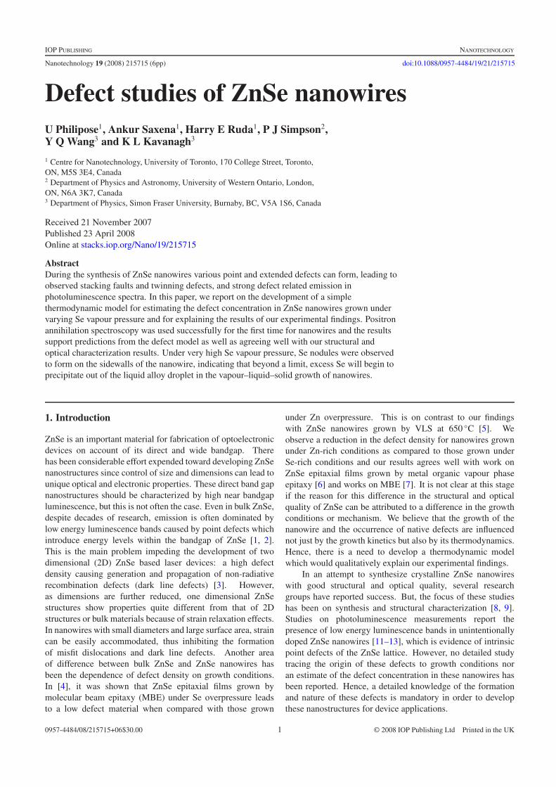
Figure 4 shows the S parameter versus positron energy(corresponds to probing depth) for ZnSe nanowires grown at650 ◦C (i) under high Se vapour pressure and (ii) under nearlystoichiometric conditions. The higher value of S obtained fromthe sample grown under high Se vapour pressure suggests thatthis sample contains a greater concentration of Zn vacancies,consistent with our defect model. It is thus evident that asthe Se vapour pressure is increased, the Zn vacancy defectconcentration increases. Caution is required in attempting a
Figure 4. S-parameter as a function of positron energy,characterizing the difference in vacancy concentration for ZnSenanowires grown at 650 ◦C under varying Se vapour flux.
quantitative interpretation of the positron data: the nanowiresdo not cover 100% of the area of the substrate, and so the dataobtained represent an average of substrate and nanowires. Themeasured change in the S parameter between the two samplesis about 2%; we would expect a maximum change of about5% if there were no vacancies in one sample, and enoughvacancies to trap 100% of the positrons (>∼1018 cm−3), in theother sample. In light of the uncertainties here, we tentativelysuggest that a lower limit on the concentration of Zn vacanciesin the sample grown under high Se vapour pressure is of theorder of 1017 cm−3. We are not able to set an upper limit onbasis of these data.
Further confirmation validating the predictions of thedefect model (figures 2 and 3) was achieved by opticalcharacterization using PL spectroscopy. A typical roomtemperature PL spectrum of ZnSe nanowires has twocharacteristic emission peaks—a band edge (BE) emissionpeak at 2.68 eV (463 nm) and a broad deep defect (DD)emission peak in the region 1.8–2.4 eV (500–680 nm).The origin of the DD emission peak has been attributedto recombination of DAPs involving Zn vacancies and Zninterstitials [17]. The PL spectra of nanowires grownunder three different growth conditions is shown in figure 5.The emission spectrum of nanowires grown under nearstoichiometric conditions, when the Se vapour pressure is closeto (P1/2
Se2)min (curve 2 in figure 5) shows that the spectrum is
comprised of two emission bands with a narrow band edge(BE) peak at 463 nm and a DD band extending from ∼500to 680 nm. The BE emission peak intensity in some cases isstronger than the DD emission intensity centred at ∼620 nm.As the Se vapour pressure is increased ((P1/2
Se2) is increased),
the emission spectra (curve 3 in figure 5) shows a completedisappearance of the BE emission peak and the PL spectrum isdominated by the DD emission peak. The amplitude of the BEemission is insignificant. These findings are consistent withthe defect model predictions shown in figure 3, that as (P1/2
Se2)
increases, the net vacancy concentration increases. Anotherinteresting feature of the plot shown in figure 3 is that as thepartial pressure of Se vapour is reduced from (P1/2
Se2)min, there
4

Nanotechnology 19 (2008) 215715 U Philipose et al
Figure 5. Room temperature PL spectra of ZnSe nanowires grownunder different growth conditions. Curve 1: when Se vapour pressureis less than (P1/2
Se2)min, the spectrum is dominated by BE emission;
curve 2: when Se vapour pressure is close to (P1/2Se2
)min, there is asignificant decrease in the intensity of the BE emission and there iscomparable DD emission; curve 3: when the Se vapour pressure isgreater than (P1/2
Se2)min, the PL spectrum shows strong DD emission
and no emission from the BE states.
Figure 6. TEM image of a single ZnSe nanowire grown underSe-rich conditions: (a) high density of stacking faults; (b) lowerdensity of stacking faults.
is a significant decrease in the net concentration of defects byseveral orders of magnitude. This was verified experimentallyby growing ZnSe nanowires under Zn-rich conditions, i.e.,when the partial pressure of Se is lower than (P1/2
Se2)min. The
PL spectra (curve 1 in figure 5) shows an enhanced BEemission with virtually no emission from the defect states. Incomparison with curve 2 in figure 5, there is an enhancementin the ratio of BE/DD emission by more than three orders ofmagnitude, in agreement with the predictions of the defectmodel.
We also observe a significant difference in the structuralcharacteristics of these nanowires when they are grown underdifferent conditions of Se vapour pressure. HRTEM ofthe nanowires grown under near stoichiometric conditions,when the Se vapour pressure is close to (P1/2
Se2)min, show
that they were crystalline and most of them contain nostacking faults or twinning defects. However, as the
Figure 7. SEM image of a ZnSe nanowire grown under very highSe vapour pressure, shows nodules appearing as outgrowths alongthe edge of the nanowire.
Figure 8. EDXS measurement: (a) along the nanowire lengthconfirms the nanowire composition to be ZnSe; (b) at the nodulealong the edge of the nanowire shows they are comprised of only Se.The circular indexed spot indicates the region of testing.
(This figure is in colour only in the electronic version)
Se vapour pressure is increased ((P1/2Se2
) is increased), thenanowires have a high density of structural defects in theform of stacking faults and twinning defects (figures 6(a)and (b)). This high density of structural defects could beattributed to an increased net defect concentration as shownin figure 3 when (P1/2
Se2) is increased. ZnSe nanowires
grown under extremely high Se vapour pressure show Se-richnodules appear as outgrowth on the edges of the nanowire(figure 7). EDXS measurements along the nanowire length(figure 8(a)) confirms that the nanowire is ZnSe, whereasthe nodules along the edge of the nanowire (figure 8(b))are comprised of only Se. Nanowires grown under reducedSe vapour pressure, with (P1/2
Se2) values lower than (P1/2
Se2)min
(figure 3) were crystalline nanowires with no structuraldefects. These results clearly demonstrate that there is adirect relationship between stoichiometry of the componentvapour flux, structural defects and optical performance of thenanowires.
5. Conclusion
Deviation from stoichiometry is shown to be one of themost critical growth conditions influencing the quality ofZnSe nanowires. We use a thermodynamic model toestimate the defect concentration in ZnSe nanowires grownby the VLS mechanism. The results from this model
5

Nanotechnology 19 (2008) 215715 U Philipose et al
is used to qualitatively explain the difference in structuraland optical properties of nanowires grown under varyingSe vapour pressure. A high concentration of point defectsresults in the formation of stacking faults and degrade theoptical properties of the nanowires, making them unsuitablefor optoelectronic applications. Positron annihilationspectroscopy and photoluminescence spectroscopy were usedto characterize the nanowires and based on our results, we canconclude that ZnSe nanowires grown at 650 ◦C, under nearstoichiometric conditions, are most ideal for the growth ofcrystalline nanowires with minimum point defects. Qualitativeanalysis of PAS data confirms that ZnSe nanowires grown athigh Se vapour pressure contains a higher concentration ofZn vacancies. At very high Se vapour pressures, Se nodulesformed along the edges of the nanowire.
Acknowledgments
The authors gratefully acknowledge financial support fromNSERC, CIPI, CITO, MMO, AFOSR and CSA.
References
[1] Kolodziejski L A, Gunshor R L and Nurmikko A V 1995Annu. Rev. Mater. Sci. 25 711
[2] Cook J W Jr and Schetzina J F 1995 Laser Focus World 31 101[3] Kim J R and Jones K S 1996 Crit. Rev. Solid State Mater. Sci.
21 1
[4] Kuo L H, Kimura K, Miwa S, Yasuda T and Yao T 1996Appl. Phys. Lett. 69 1408
[5] Philipose U, Xu T, Yang S, Sun P, Ruda H E, Wang Y andKavanagh K L 2006 J. Appl. Phys. 100 084316
[6] Yodo T, Koyama T and Yamashita K 1988 J. Appl. Phys.64 2403
[7] DePuydt J M, Cheng H, Potts J E, Smith T L andMohapatra S K 1987 J. Appl. Phys. 62 4756
[8] Ye C, Fang X, Wang Y, Yan P, Zhao J and Zhang L 2004Appl. Phys. A 79 113
[9] Duan X F and Lieber C M 2000 Adv. Mater. 12 298[10] Li Q, Gong X, Wang C, Wang J, Ip K and Hark S 2004
Adv. Mater. 16 1436[11] Zhu Y and Bando Y 2003 Chem. Phys. Lett. 377 367[12] Xiang B et al 2003 Appl. Phys. Lett. 82 3330[13] Zhang X T, Liu Z, Ip K M, Leung Y P, Li Q and
Hark S K 2004 J. Appl. Phys. 95 5752[14] Laks D B, Van de Walle C G, Neumark G F, Blochl P E and
Pantelides S T 1992 Phys. Rev. B 45 10965[15] Kroger F A 1977 Annu. Rev. Mater. Sci. 7 449[16] Rong F and Watkins G D 1986 Phys. Rev. Lett. 56 2310[17] Philipose U, Yang S, Xu T and Ruda H E 2007 Appl. Phys.
Lett. 90 063103[18] Asoka-Kumar P, Lynn K G and Welch D O 1994 J. Appl. Phys.
76 4935[19] Reschikov M A and Morkoc H 2005 J. Appl. Phys. 97 061301[20] Van de Walle C G and Neugebauer J 2004 J. Appl. Phys.
95 3851[21] Chadi D J 1994 Annu. Rev. Mater. Sci. 24 45[22] Hartmann H, Mach R and Selle B 1982 Current Topics in
Materials Science vol 9, ed E Kaldis (Amsterdam:North-Holland)
[23] Van Gool W 1966 Principles of Defect Chemistry of CrystallineSolids (New York: Academic)
6