growth and characterisation of textured
TRANSCRIPT
GROWTH AND CHARACTERISATION OF
TEXTURED SUPERCONDUCTING TAPES
By
Shadi Mohammad Abdel Kareem Al Khateeb
A thesis submitted to The University of Birmingham for the degree of
DOCTOR OF PHILOSOPHY
Department of Metallurgy and Materials The University of Birmingham November 2009

University of Birmingham Research Archive
e-theses repository This unpublished thesis/dissertation is copyright of the author and/or third parties. The intellectual property rights of the author or third parties in respect of this work are as defined by The Copyright Designs and Patents Act 1988 or as modified by any successor legislation. Any use made of information contained in this thesis/dissertation must be in accordance with that legislation and must be properly acknowledged. Further distribution or reproduction in any format is prohibited without the permission of the copyright holder.
Abstract MgO thin films were deposited on Si (100) single crystals, NiW tapes,
310-austenitic stainless steel and Hastelloy C276 by the ultrasonic Spray Pyrolysis
technique, using magnesium nitrate and magnesium acetate as precursors at many
different conditions. Thermogravimetrical analysis (TGA) of the decomposition of the
precursors was used as a guideline temperature for the thin film deposition. Biaxially
textured and epitaxial MgO films were deposited on Si substrates using magnesium
nitrate precursors. An amorphous MgO thin film was deposited on NiW tapes, NiO
buffered NiW, 310-stainless steel and Hastelloy C276 when using low concentration of
the magnesium nitrate precursor. Higher concentrations were needed to obtain (200)
oriented MgO films on C276. However, NiW tapes and 310-stainless steel were found to
be a non suitable substrate for MgO thin film deposition due to surface instability. A
(200) oriented MgO thin film was grown on Hastelloy C276 using a magnesium acetate
precursor at a much lower concentration compared to the nitrate precursor. The ISD
deposition by spray pyrolysis (irrespective of the used precursor and the used substrate)
produced MgO films that grew with the (200) normal to substrate surface as distinct to
MgO films grown by thermal evaporation which grew with the (200) tilted to the
substrate normal. Pulsed laser deposition (PLD) was used to deposit YBCO on
MgO-buffered substrates. The characterization of the thin films was done using SEM,
EBSD, XPS, AFM, X-ray diffraction 2θ-scans, rocking curve (ω-scans), phi (φ) scans, X-
ray pole-figure measurements, and AC susceptibility. YBCO deposition by PLD on Si
substrates buffered with MgO was not successful due to the thermal stresses developed in
the MgO buffer. An EDX line scan performed on MgO films deposited on Hastelloy
C276 from the acetate precursors confirmed the effectiveness of such layer as a diffusion
barrier. It was found that c-axis oriented YBCO films were grown on c-axis oriented
MgO films deposited on C276 from the nitrate and acetate precursors; however, MgO and
YBCO films have a very weak in-plane texture. The AC susceptibility measurements
show that the YBCO films have a broad superconducting transition temperature
irrespective of the precursor used. To improve the superconducting transition
temperatures, different annealing treatments were performed on the MgO buffer deposited
on Hastelloy C276, however, it was found that the as deposited MgO buffer films and
subsequent deposition of YBCO films gave the best superconducting transition
temperatures. In an attempt to improve the in-plane texture of YBCO, CeO2 was
deposited by PLD on the spray pyrolysed MgO.

To my parents, my wife and my children

Acknowledgements A great acknowledgment goes to my supervisors Prof. J.S. Abell and Prof. T.W.
Button for their invaluable advices, sincere teaching and their kindness during the
preparation of this thesis.
Thanks to Dr. Elizabeth Blackburn, from the Physics dept. for her help and
giving access to the D5000 diffractometer for doing the rocking curve and phi scans
measurements. Thanks to Dr. Tim Jackson from the electronic, electrical and
computing engineering dept. for his help and giving the access to the laser laboratory.
I would like also to thank Dr. Yau Yau Tse, Dr. Chris Cooper, Dr. Seyed
Koohpayeh, and Dr. Santiago Corujeira Gallo for their help in performing some of the
needed experiments.
Thanks to Mr. Andy Bradshaw for his technical support. Thanks to my
colleagues who supported me through the friendly chats and especially to Joe Tanner
who helped me doing some laser depositions.
I would like to thank the Overseas Research Scholarship Award Scheme
(ORSAS) and the Department of Metallurgy and Materials who covered jointly my
tuition fees.
Finally, I would like to thank my parents, my wife and my brothers and sisters
who stood behind my step by step until I finished my PhD.

Publications 1. Pavlopoulos D, Shadi Al-Khatiab, Button TW, Abell JS. Effort to produce
textured CeO2 and MgO films by the spray pyrolysis technique as buffer layers for coated conductors. Journal of Physics: Conference Series. 2008;97:012098.
2. Shadi Al Khateeb, T.W. Button, J.S. Abell. Spray pyrolysis of MgO templates
on Hastelloy C276 and 310-austenitic stainless steel substrates for YBa2Cu3O7 (YBCO) deposition by PLD. To be published.
3. D. Pavlopoulos, Shadi Al-Khateeb, T. W. Button, Abell JS. Spray Pyrolysis of
Ceria (CeO2) Thin Films and the Effect of Deposition Parameters on the Textural and Structural Properties. To be published.
4. D. Pavlopoulos, Shadi Al-Khateeb, T. W. Button, J. S. Abell. Spray Pyrolysis
of MgO Thin Films on Si Single Crystals and the Effect of Deposition Time and Inclination Angle on the Texture and Morphology of the Films. To be published.
It should be mentioned that the first, third and fourth publications are not part of
the experimental results presented in this thesis. However, these articles are used as
references, within this thesis.
Table of contents
1 Introduction............................................................................................................... 1 2 Theory and literature review ................................................................................... 5
2.1 Superconductivity ................................................................................................ 6 2.1.1 History......................................................................................................... 6 2.1.2 Meissner effect............................................................................................ 7 2.1.3 Type I and type II superconductors ............................................................ 8 2.1.4 Coated conductor tapes ............................................................................... 8
2.1.4.1 The substrate layer .................................................................................... 10 2.1.4.2 The buffer layer......................................................................................... 14 2.1.4.3 The superconducting layer ........................................................................ 16
2.2 Thin film technology.......................................................................................... 18 2.2.1 Epitaxy ...................................................................................................... 20
2.3 Spray pyrolysis for film formation .................................................................... 23 2.4 Aerosol techniques............................................................................................. 30
2.4.1 Technologies for generating powders and films....................................... 31 2.4.1.1 Gas to particle conversion......................................................................... 31
2.4.1.1.1 Mean free path of the gas................................................................ 33 2.4.1.2 Intraparticle reaction processes................................................................. 35
2.4.2 Chemistry of aerosol processes................................................................. 37 2.4.2.1 Thermal decomposition of precursors ...................................................... 40 2.4.2.2 Surface processes ...................................................................................... 41
2.4.3 Particle growth, evaporation and nucleation phenomena in aerosols ....... 42 2.4.3.1 Introduction............................................................................................... 42 2.4.3.2 Qualitative particle growth ....................................................................... 43
2.4.3.2.1 Chemical reactions.......................................................................... 46 2.4.3.3 Droplet evaporation .................................................................................. 48 2.4.3.4 Nucleation ................................................................................................. 50
2.4.4 Advantages and disadvantages of aerosol processes for thin film deposition.................................................................................................. 51
2.5 Spray pyrolysis of magnesium oxide (MgO) .................................................... 52 2.5.1 Substrate temperature, carrier gas flow rate and spray rate ...................... 52 2.5.2 Substrate- nozzle distance (SND) ............................................................ 56 2.5.3 Solution concentration .............................................................................. 57 2.5.4 Different methodological approaches for the deposition of MgO ............ 58 2.5.5 Spray pyrolysis of other ceramic oxides................................................... 59
2.6 ISD deposition of MgO using e-beam evaporation ........................................... 75 2.7 MgO deposition on Si substrates by PLD.......................................................... 78 2.8 MgO surface optimization for YBa2Cu3O7 (YBCO) thin film growth and
YBCO defects .................................................................................................... 78 3 Experimental details ............................................................................................... 83
3.1 The spray pyrolysis unit..................................................................................... 84 3.1.1 The deposition substrates .......................................................................... 87 3.1.2 MgO film deposition................................................................................. 87
3.2 Pulsed laser deposition (PLD) .......................................................................... 87 3.3 Characterization techniques ............................................................................... 89
3.3.1 Thermogravimetrical analysis................................................................... 89 3.3.2 X-ray diffraction (XRD) .......................................................................... 90

3.3.3 Scanning electron microscopy (SEM) ..................................................... 92 3.3.3.1 Energy dispersive spectroscopy (EDS) .................................................... 94 3.3.3.2 Electron backscattered diffraction (EBSD) ............................................. 95
3.3.4 Atomic force microscopy (AFM) ............................................................ 98 3.3.5 AC susceptibility..................................................................................... 100 3.3.6 X-ray photoelectron spectroscopy (XPS) .............................................. 102
4 Spray pyrolysis of MgO on silicon single crystals using magnesium nitrate as a precursor ....................................................................................................... 103
4.1 Introduction...................................................................................................... 104 4.2 Thermal decomposition of the nitrate precursor .............................................. 104 4.3 MgO deposition by spray pyrolysis on Si (100) substrates ............................. 105
4.3.1 Effect of substrate temperature and precursor concentration on MgO film properties ......................................................................................... 106
4.3.2 Surface morphology................................................................................ 109 4.3.3 Composition of films and texture analysis.............................................. 116 4.3.4 Effect of inclination angle on MgO film properties................................ 118 4.3.5 Effect of deposition parameters on MgO film thickness ........................ 133
4.4 MgO deposition by pulsed laser deposition on Si (100) substrates ................. 138 4.5 Optimisation of YBCO deposition parameters ................................................ 141
4.5.1 YBCO deposition by pulsed laser deposition on MgO single crystals ... 145 4.6 YBCO deposition by pulsed laser deposition on Si (100) substrates buffered
with MgO......................................................................................................... 157 5 Spray Pyrolysis of MgO on RABiTS NiW.......................................................... 162
5.1 Introduction...................................................................................................... 163 5.2 NiW substrates ................................................................................................. 163 5.3 Recrystallisation treatment of NiW substrates................................................. 165 5.4 MgO deposition on NiW RABiTS by spray pyrolysis using magnesium
nitrate precursor ............................................................................................... 170 5.5 Growth of textured NiO films on NiW RABiTS ............................................. 173 5.6 MgO deposition on (200) textured NiO by spray pyrolysis using magnesium
nitrate precursor ............................................................................................... 178 6 Spray pyrolysis of MgO on 310-austenitic stainless steel using magnesium
nitrate as a precursor........................................................................................... 182 6.1 Introduction...................................................................................................... 183 6.2 310-stainless steel substrates............................................................................ 183 6.3 Spray pyrolysis of MgO on 310-austenitic stainless using magnesium nitrate
precursor .......................................................................................................... 186 6.3.1 Effect of deposition temperature and time on MgO film properties....... 186 6.3.2 Effect of precursor concentration on MgO film properties .................... 191
6.4 Detecting susceptibility to intergranular attack in 310-austenitic stainless steel .................................................................................................................. 193
6.4.1 ASTM A 262: practice A-oxalic acid etch of austenitic stainless steels 195 6.4.2 Oxalic acid etch of 310- austenitic stainless steel................................... 196
7 Spray pyrolysis of MgO on Hastelloy C276 from nitrate precursor................ 201 7.1 Introduction...................................................................................................... 202 7.2 Susceptibility of Hastelloy C276 to intergranular corrosion ........................... 202
7.2.1 Introduction............................................................................................. 202 7.2.2 Hastelloy C276 substrates....................................................................... 202 7.2.3 Detecting susceptibility to intergranular attack in Hastelloy C276 ........ 205

7.2.3.1 BSI BS EN ISO 9400:1995, method A (corresponds to the ASTM standard G28, method A) ....................................................................... 206
7.2.3.2 Ferric sulfate – sulfuric acid test for Hastelloy C276 ............................. 208 7.3 Spray pyrolysis of MgO from the nitrate precursor......................................... 213 7.4 Effect of deposition temperature on MgO film properties............................... 214 7.5 Effect of deposition time on MgO film properties........................................... 218 7.6 Effect of precursor concentration on MgO film properties ............................. 221 7.7 X-ray photoelectron spectroscopy (XPS) test.................................................. 231 7.8 Effect of deposition parameters on MgO film thickness ................................. 232 7.9 Effect of inclination angle (ISD) on MgO film properties .............................. 235 7.10 Effect of Ar flow rate on MgO film properties................................................ 239 7.11 Effect of annealing on the texture of MgO films............................................. 243
7.11.1 Annealing under O2 atmosphere ............................................................. 243 7.11.2 Annealing under vacuum ........................................................................ 250
7.12 YBCO, MgO and ceria (CeO2) deposition by PLD......................................... 261 7.12.1 Introduction............................................................................................. 261 7.12.2 YBCO deposition on MgO films spray pyrolysed at different
temperatures, precursor concentrations and deposition times ................ 261 7.12.3 Pulsed laser deposition of MgO on bare Hastelloy substrates................ 272 7.12.4 Pulsed laser deposition of ceria (CeO2) and YBCO on MgO
deposited by spray pyrolysis ................................................................... 273 8 Spray pyrolysis of MgO on Hastelloy C276 from acetate precursor ............... 283
8.1 Introduction...................................................................................................... 284 8.2 MgO deposition on Hastelloy C276 from acetate precursor ........................... 284
8.2.1 Thermal decomposition of the acetate precursor .................................... 285 8.3 Effect of deposition temperature on MgO film properties............................... 286 8.4 Effect of deposition time on MgO film properties........................................... 295 8.5 Effect of precursor concentration on MgO film properties ............................. 301 8.6 X-ray photoelectron spectroscopy (XPS) test.................................................. 304 8.7 Effect of deposition parameters on MgO film thickness ................................. 307 8.8 Effect of inclination angle (ISD) on MgO film properties .............................. 307 8.9 Effect of Ar flow rate on MgO film properties................................................ 312 8.10 Effect of annealing on the texture of MgO films............................................. 315
8.10.1 Annealing under O2 atmosphere ............................................................. 315 8.10.2 Annealing under vacuum ........................................................................ 320
8.11 YBCO and ceria (CeO2) deposition by PLD ................................................... 326 8.11.1 Introduction............................................................................................. 326 8.11.2 YBCO deposition on MgO spray pyrolysed at different temperatures,
precursor concentrations and deposition times. ..................................... 326 8.11.3 Pulsed laser deposition of Ceria (CeO2) and YBCO on MgO deposited
by spray pyrolysis ................................................................................... 344 9 Conclusions and future work............................................................................... 352
9.1 Introduction...................................................................................................... 353 9.1.1 Depositions on Si (100) single crystals using magnesium nitrate
precursor ................................................................................................. 353 9.1.2 Depositions on NiW tapes using magnesium nitrate and acetate
precursors................................................................................................ 354 9.1.3 Depositions on 310-austenitic stainless steel using magnesium nitrate
precursor ................................................................................................. 355 9.1.4 Depositions on Hastelloy C276 .............................................................. 355

9.1.4.1 MgO deposition from the nitrate precursor ............................................ 355 9.1.4.2 MgO deposition from the acetate precursor............................................ 357
9.2 Suggestions for future work............................................................................. 359 9.2.1 Deposition of MgO thin films................................................................. 359 9.2.2 System modification ............................................................................... 361
List of References…………………….…………………………………………..362

List of Figures
Figure 2.1: Vanishing of resistance below Tc [9].
Figure 2.2: Discovery of superconducting materials over the last century [9].
Figure 2.3: Magnetic field expulsion below Hc [9].
Figure 2.4: Schematic diagram for type I and type II superconductors [15].
Figure 2.5: Superconductor architecture [28].
Figure 2.6: Ratio of grain boundary critical current density gbCJ to the average value
of the critical current density GCJ as a function of the misorientation angle [30].
Figure 2.7: Schematics of the RABiTS technique. Starting with a randomly oriented Ni bar/plate, cold-rolling is used to produce a distinct rolling texture (see schematic pole figures). This is followed by recrystallisation to a cube texture. Epitaxial metal and/or oxide buffer layer(s) are then deposited on the textured Ni. [35, 37].
Figure 2.8: Textured substrate preparation by IBAD [26].
Figure 2.9: Schematic diagram of inclined substrate deposition (ISD) [40].
Figure 2.10: Unit cell for MgO having NaCl structure [62].
Figure 2.11: The unit cell of YBCO-123 [82].
Figure 2.12: Superconducting transition temperature (Tc) as a function of oxygen content for YBa2Cu3O7-x [83].
Figure 2.13: Schematic representation of the five crystal growth modes frequently occurring on flat surfaces of substrate crystals: (a) layer-by-layer or Frank-van der Merve, (b) step flow, (c) layer plus island or Stranski-Krastanov, (d) island or Volmer-Weber, (e) columnar growth mode. θ represents the coverage in monolayers (ML) [94].
Figure 2.14: Schematic diagram of the spray pyrolysis equipment [68].
Figure 2.15: Dependence of droplet size on transducer frequency [96].
Figure 2.16: Number (dotted)) and volume (solid) distribution of water droplets [105, 106].
Figure 2.17: Dependence of aerosol flow as a function of liquid level above transducer [105].
Figure 2.18: Droplets of different sizes can behave differently during deposition [96].
Figure 2.19: Possible working modes that may occur during deposition [67].
Figure 2.20: Possible behaviour modes of AACVD [96].
Figure 2.21: Schematic of the impaction mechanism [109].
Figure 2.22: Role of particle deposition in various processes for film fabrication [96].

Figure 2.23: Particle transport phenomena [96].
Figure 2.24: Relation between particle sizes and mean free path for a) continuum regime and b) free molecular regime [96].
Figure 2.25: Production of thin films by spray pyrolysis [96].
Figure 2.26: Schematic of atoms and / or molecules (A) colliding with a particle in the free molecular regime [96].
Figure 2.27: Schematic illustrating how atoms and molecules are transported to a particle surface by diffusion in the continuum regime [96].
Figure 2.28: Decomposition as a function of temperature [106].
Figure 2.29: Schematic diagram showing the principle of ISD deposition (left) and schematic diagram showing the growth of crystals truncated by (200) planes (right) [162].
Figure 3.1: Schematic of the ultrasonic nebuliser [200].
Figure 3.2: Schematic of the spray pyrolysis reactor [133].
Figure 3.3: A photograph of the spray pyrolysis system showing, from left to right, the gas flow meter, the thermocouple, the temperature controller, the tubular furnace and the ultrasonic nebuliser.
Figure 3.4: Schematic of the ISD setup.
Figure 3.5: Schematic of the PLD system [201].
Figure 3.6: Image of the used PLD system.
Figure 3.7: Schematic of X-ray diffractometer [204].
Figure 3.8: Schematic showing the φ and ψ rotations during pole figure measurements [204].
Figure 3.9: Electron beam-specimen interaction [206].
Figure 3.10: A JEOL 7000 scanning electron microscope.
Figure 3.11: Schematic of the energy dispersive spectrometer [208].
Figure 3.12: An image showing a tilted sample and a phosphorous screen in SEM chamber [209].
Figure 3.13: EBSD geometry [209].
Figure 3.14: Schematic of the contact mode AFM [211].
Figure 3.15: Schematic of AC susceptibility apparatus.
Figure 3.16: χ/ and χ// for YBCO deposited on MgO single crystal with a TC onset of 90.2K.
Figure 4.1: TGA curve for Mg(NO3)2.6H2O.

Figure 4.2: XRD patterns of the MgO films deposited with zero inclination angle, at different temperatures, from 0.0078M Mg(NO3)2.6H2O solution.
Figure 4.3: XRD patterns of the MgO film deposited with zero inclination angle, at different temperatures, from 0.078M Mg(NO3)2.6H2O solution.
Figure 4.4: SEM image of the MgO film deposited with a zero inclination angle at 650°C from 0.0078M Mg(NO3)2.6H2O solution.
Figure 4.5: SEM image of the MgO film deposited with a zero inclination angle at 650°C from 0.078M Mg(NO3)2.6H2O solution.
Figure 4.6: SEM image of the MgO film deposited with a zero inclination angle at 700°C from 0.0078M Mg(NO3)2.6H2O solution.
Figure 4.7: SEM image of the MgO film deposited with a zero inclination angle at 700°C from 0.078M Mg(NO3)2.6H2O solution.
Figure 4.8: A 5x5µm2 AFM image of the MgO film deposited with a zero inclination angle at 650°C from 0.0078M Mg(NO3)2.6H2O solution.
Figure 4.9: A 5x5µm2 AFM image of the MgO film deposited with a zero inclination angle at 650°C from 0.078M Mg(NO3)2.6H2O solution.
Figure 4.10: A 5x5µm2 AFM image of the MgO film deposited with a zero inclination angle at 700°C from 0.0078M Mg(NO3)2.6H2O solution.
Figure 4.11: A 5x5µm2 AFM image of the MgO film deposited with a zero inclination angle at 700°C from 0.078M Mg(NO3)2.6H2O solution.
Figure 4.12: AFM section profile image of the MgO film deposited with a zero inclination angle at 650°C from 0.078M Mg(NO3)2.6H2O solution.
Figure 4.13: AFM section profile image of the MgO film deposited with a zero inclination angle at 700°C from 0.078M Mg(NO3)2.6H2O solution.
Figure 4.14: EDX spectrum for the sample deposited at 650°C from 0.078M solution using an accelerating voltage of 4KV.
Figure 4.15: (400), left, and (111), right, X-ray pole figures, at 2θ of 69.17° and 28.42°, respectively, of Si (100) substrate deposited with MgO film at 650°C using 0.078M solution.
Figure 4.16: (200), left, and (111), right, X-ray pole figures, at 2θ of 43.85° and 36.93°, respectively, of the MgO film deposited at 650°C using 0.078M solution.
Figure 4.17: XRD patterns of the MgO films deposited at different inclination angles, at 650°C from a 0.0078M Mg(NO3)2.6H2O solution.
Figure 4.18: XRD patterns of the MgO films deposited at different inclination angles, at 650°C from a 0.078M Mg(NO3)2.6H2O solution.
Figure 4.19: RMS roughness of the MgO films deposited at 650°C from 0.0078M and 0.078M Mg(NO3)2.6H2O solution.

Figure 4.20: SEM image of the MgO film deposited at 650°C from a solution of 0.0078M at an inclination angle of 20°.
Figure 4.21: SEM image of the MgO film deposited at 650°C from a solution of 0.0078M at an inclination angle of 45°.
Figure 4.22: SEM image of the MgO film deposited at 650°C from a solution of 0.0078M at an inclination angle of 60°.
Figure 4.23: SEM image of the MgO film deposited at 650°C from a solution of 0.078M at an inclination angle of 20°.
Figure 4.24: SEM image of the MgO film deposited at 650°C from a solution of 0.078M at an inclination angle of 45°.
Figure 4.25: SEM image of the MgO film deposited at 650°C from a solution of 0.078M at an inclination angle of 60°.
Figure 4.26: A 5x5µm2 AFM image of the MgO film deposited at 650°C from a solution of 0.078M at an inclination angle of 60°.
Figure 4.27: (400), left, and (111), right, X-ray pole figures, at 2θ of 69.17° and 28.42°, respectively, of Si (100) substrate deposited with MgO film at 650°C from a solution of 0.078M at an inclination angle of 20°.
Figure 4.28: (200), left, and (111), right, X-ray pole figures, at 2θ of 43.82° and 36.93°, respectively, of the MgO film deposited at 650°C from a solution of 0.078M at an inclination angle of 20°.
Figure 4.29: XRD patterns of the MgO films deposited at different inclination angles, at 700°C from a 0.0078M Mg(NO3)2.6H2O solution.
Figure 4.30: XRD patterns of the MgO films deposited at different inclination angles, at 700°C from a 0.078M Mg(NO3)2.6H2O solution.
Figure 4.31: RMS roughness of the MgO films deposited at 700°C from 0.0078m and 0.078M Mg(NO3)2.6H2O solution.
Figure 4.32: SEM image of the MgO film deposited at 700°C from a solution of 0.0078M at an inclination angle of 20°.
Figure 4.33: SEM image of the MgO film deposited at 700°C from a solution of 0.0078M at an inclination angle of 45°.
Figure 4.34: SEM image of the MgO film deposited at 700°C from a solution of 0.0078M at an inclination angle of 60°.
Figure 4.35: SEM image of the MgO film deposited at 700°C from a solution of 0.078M at an inclination angle of 20°.
Figure 4.36: SEM image of the MgO film deposited at 700°C from a solution of 0.078M at an inclination angle of 45°.
Figure 4.37: SEM image of the MgO film deposited at 700°C from a solution of 0.078M at an inclination angle of 60°.

Figure 4.38: (400), left, and (111), right, X-ray pole figures, at 2θ of 69.17° and 28.42°, respectively, of Si (100) substrate deposited with MgO film at 700°C from a solution of 0.078M at an inclination angle of 20°.
Figure 4.39: (200), left, and (111), right, X-ray pole figures, at 2θ of 43.96° and 36.93°, respectively of the MgO film deposited at 700°C from a solution of 0.078M at an inclination angle of 20°.
Figure 4.40: Effect of deposition temperature and precursor concentration on MgO film thicknesses deposited with zero inclination angle.
Figure 4.41: A cross sectional SEM image for MgO film deposited at 600°C from 0.0078M solution.
Figure 4.42: A cross sectional SEM image for MgO film deposited at 650°C from 0.078M solution with an inclination angle of 45°.
Figure 4.43: Effect of inclination angle and precursor concentration on MgO film thicknesses (at a deposition temperature of 650°C).
Figure 4.44: effect of inclination angle and precursor concentration on MgO film thicknesses (at a deposition temperature of 700°C).
Figure 4.45: A cross section image for MgO film deposited at 700°C from 0.078M solution with an inclination angle of 20°.
Figure 4.46: XRD patterns for MgO deposition on Si (100) substrate by PLD at different fluencies and compared to MgO deposition by spray pyrolysis using 0.078M of magnesium nitrate at 650°C with zero inclination angle.
Figure 4.47: SEM image for MgO film deposited by PLD on Si (100) at an energy fluence of 3.45J/cm2.
Figure 4.48: A 5x5µm2 AFM image for MgO film deposited by PLD on Si (100) at an energy fluence of 3.45J/cm2.
Figure 4.49: (200) X-ray pole figure at 2θ=43.10° of the MgO film deposited by PLD on Si (100) at an energy fluence of 3.45J/cm2.
Figure 4.50: XRD pattern of the as received MgO single crystal.
Figure 4.51: SEM image of the as received MgO single crystal.
Figure 4.52: A 5x5µm2 AFM image of the as received MgO single crystal.
Figure 4.53: EBSD pole figure patterns for MgO single crystal showing the MgO {100}, {110} and {111} planes.
Figure 4.54: X-ray diffraction ω−scan for MgO (200) with a FWHM of 0.025ο.
Figure 4.55: X-ray diffraction Φ−scan for MgO (220) with a FWHM of about 0.038ο.
Figure 4.56: XRD patterns for YBCO films deposited on MgO single crystal using different number of pulses and different fluencies.
Figure 4.57: XRD patterns in log scale for YBCO films deposited on MgO single crystal using different number of pulses and different fluencies.

Figure 4.58: SEM image for a 2000 pulses YBCO film deposited on MgO single crystal using a fluence of 2 J/cm2.
Figure 4.59: SEM image for a 2000 pulses YBCO film deposited on MgO single crystal using a fluence of 2.75 J/cm2.
Figure 4.60: A 5x5µm2 AFM image for a 2000 pulses YBCO film deposited on MgO single crystal using a fluence of 2 J/cm2.
Figure 4.61: A 5x5µm2 AFM image for a 2000 pulses YBCO film deposited on MgO single crystal using a fluence of 2.75 J/cm2.
Figure 4.62: EBSD pole figure patterns for a 2000 pulses YBCO film deposited on MgO single crystal using a fluence of 2 J/cm2 showing the YBCO {006} and {103} planes.
Figure 4.63: EBSD pole figure patterns for a 2000 pulses YBCO film deposited on MgO single crystal using a fluence of 2.75 J/cm2 showing the YBCO {006} and {103} planes.
Figure 4.64: EBSD histogram for a 2000 pulses YBCO film deposited on MgO single crystal using a fluence of 2J/cm2 showing misorientation angles.
Figure 4.65: EBSD histogram for a 2000 pulses YBCO film deposited on MgO single crystal using a fluence of 2.75J/cm2 showing misorientation angles.
Figure 4.66: SEM image for a 5000 pulses YBCO film deposited on MgO single crystal using a fluence of 2 J/cm2.
Figure 4.67: SEM image for a 10000 pulses YBCO film deposited on MgO single crystal using a fluence of 2 J/cm2.
Figure 4.68: A 5x5µm2 AFM image for a 5000 pulses YBCO film deposited on MgO single crystal using a fluence of 2 J/cm2.
Figure 4.69: A 5x5µm2 AFM image for a 10000 pulses YBCO film deposited on MgO single crystal using a fluence of 2 J/cm2.
Figure 4.70: A cross sectional SEM image for a 10000 pulses YBCO film deposited on MgO single crystal using a fluence of 2 J/cm2.
Figure 4.71: EBSD pole figure patterns for a 5000 pulses YBCO film deposited on MgO single crystal using a fluence of 2 J/cm2 showing the YBCO {006} and {013} planes.
Figure 4.72: EBSD pole figure patterns for a 10000 pulses YBCO film deposited on MgO single crystal using a fluence of 2 J/cm2 showing the YBCO {006} and {103} planes.
Figure 4.73: X-ray diffraction ω−scan for a 5000 pulses YBCO film deposited on MgO single crystal using a fluence of 2J/cm2 showing a FWHM of 1.03ο.
Figure 4.74: X-ray diffraction Φ−scan for a 5000 pulses YBCO film deposited on MgO single crystal using a fluence of 2J/cm2 showing a FWHM of 1.8ο.

Figure 4.75: EBSD histogram for a 5000 pulses YBCO film deposited on MgO single crystal using a fluence of 2J/cm2 showing misorientation angles.
Figure 4.76: AC susceptibility test showing χ/ for YBCO films deposited on MgO single crystal at different number of pulses and different fluencies.
Figure 4.77: XRD pattern for YBCO film deposited on Si (100) buffered with MgO spray pyrolysed at 650°C using 0.078M solution of magnesium nitrate at zero inclination angle.
Figure 4.78: EBSD pole figure pattern showing the {006} planes for YBCO film deposited on Si (100) buffered with MgO spray pyrolysed at 650°C using 0.078M solution of magnesium nitrate at zero inclination angle.
Figure 4.79: SEM image for YBCO film deposited on Si (100) buffered with MgO spray pyrolysed at 650°C using 0.078M solution of magnesium nitrate at zero inclination angle.
Figure 4.80: A 5x5µm2 AFM image for YBCO film deposited on Si (100) buffered with MgO spray pyrolysed at 650°C using 0.078M solution of magnesium nitrate at zero inclination angle.
Figure 4.81: AC susceptibility test showing χ/ for YBCO film deposited on Si (100) buffered with MgO spray pyrolysed at 650°C using 0.078M solution of magnesium nitrate at zero inclination angle.
Figure 5.1: A 5x5µm2 AFM image of the as received NiW substrates.
Figure 5.2: XRD pattern of the as received NiW substrates.
Figure 5.3: XRD pattern of the as received NiW substrates after the recrystallisation treatment.
Figure 5.4: (200), left, and (111), right, X-ray pole figures, at 2θ of 51.6° and 44.5°, respectively, of the as received NiW substrates after the recrystallisation treatment.
Figure 5.5: SEM image of the as received NiW substrate after the recrystallisation treatment.
Figure 5.6: A 5x5µm2 AFM image of the as received NiW substrates after the recrystallisation treatment.
Figure 5.7: SEM image of the as received NiW substrates after the recrystallisation treatment and mechanical polish.
Figure 5.8: A 5x5µm2 AFM image of the as received NiW substrates after the recrystallisation treatment and mechanical polish.
Figure 5.9: log scale XRD patterns for MgO deposition on polished and unpolished NiW substrate tapes by spray pyrolysis at 650°C using 0.468M Mg(NO3)2.6H2O for 32 minutes.
Figure 5.10: SEM image for the unpolished NiW tape deposited with 0.468M at 650°C with a deposition time of 32 minutes.
Figure 5.11: SEM image for the polished NiW tape deposited with 0.468M at 650°C with a deposition time of 32 minutes.
Figure 5.12: EDX spectrum, using an accelerating voltage of 4KV, for the polished NiW tape deposited with 0.468M at 650°C with a deposition time of 32 minutes.
Figure 5.13: XRD patterns for the unpolished NiW after recrystallisation and after recrystallisation and oxidation at different times.
Figure 5.14: SEM image for recrystallised NiW RABiTS after oxidation for 1 hour..
Figure 5.15: SEM image for recrystallised NiW RABiTS after oxidation for 3 hours.
Figure 5.16: A 30x30µm2 AFM image for recrystallised NiW RABiTS after oxidation for 1 hour.
Figure 5.17: A 30x30µm2 AFM image for recrystallised NiW RABiTS after oxidation for 3 hours.
Figure 5.18: (200), (left), and (111), (right), X-ray pole figures, at 2θ of 51.6° and 44.5°, respectively, of NiW after the recrystallisation treatment.
Figure 5.19: (200), (left), and (111), (right), X-ray pole figures, at 2θ of 43.3° and 37.3°, respectively, of NiO oxide layer (oxidised for 1 hour) on top of the recrystallised NiW shown in Figure 5.18.
Figure 5.20: XRD pattern of the recrystallised and polished NiW substrate after YBCO-thermal cycle.
Figure 5.21: SEM image of the recrystallised and polished NiW substrate after YBCO-thermal cycle.
Figure 5.22: log scale XRD pattern for MgO deposition on NiO grown on unpolished and recrystallised NiW substrate tape by spray pyrolysis at 650°C using 0.468M Mg(NO3)2.6H2O for 32 minutes.
Figure 5.23: SEM image for MgO deposition on NiO grown on unpolished and recrystallised NiW substrate tape by spray pyrolysis at 650°C using 0.468M Mg(NO3)2.6H2O for 32 minutes.
Figure 5.24: A 5x5µm2 AFM image for MgO deposition on NiO grown on unpolished and recrystallised NiW substrate tape by spray pyrolysis at 650°C using 0.468M Mg(NO3)2.6H2O for 32 minutes.
Figure 6.1: A 5x5µm2 AFM image of the mechanically polished 310-St. St substrate.
Figure 6.2: SEM image of the mechanically polished 310-St. St. substrate.
Figure 6.3: XRD pattern of the mechanically polished 310-St. St. substrate with the peaks being indexed according to the structure factor rule.
Figure 6.4: XRD patterns for MgO deposited on 310-St. St. using 0.078M of Mg(NO3)2.6H2O at different temperatures for 32 minutes.
Figure 6.5: XRD patterns for MgO deposited on 310-St. St. using 0.078M of Mg(NO3)2.6H2O at 650°C with different deposition times.
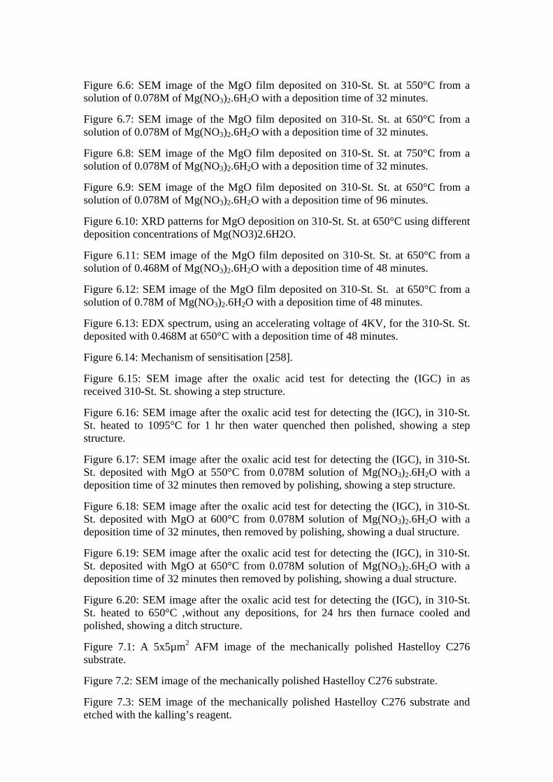
Figure 6.6: SEM image of the MgO film deposited on 310-St. St. at 550°C from a solution of 0.078M of Mg(NO3)2.6H2O with a deposition time of 32 minutes.
Figure 6.7: SEM image of the MgO film deposited on 310-St. St. at 650°C from a solution of 0.078M of Mg(NO3)2.6H2O with a deposition time of 32 minutes.
Figure 6.8: SEM image of the MgO film deposited on 310-St. St. at 750°C from a solution of 0.078M of Mg(NO3)2.6H2O with a deposition time of 32 minutes.
Figure 6.9: SEM image of the MgO film deposited on 310-St. St. at 650°C from a solution of 0.078M of Mg(NO3)2.6H2O with a deposition time of 96 minutes.
Figure 6.10: XRD patterns for MgO deposition on 310-St. St. at 650°C using different deposition concentrations of Mg(NO3)2.6H2O.
Figure 6.11: SEM image of the MgO film deposited on 310-St. St. at 650°C from a solution of 0.468M of Mg(NO3)2.6H2O with a deposition time of 48 minutes.
Figure 6.12: SEM image of the MgO film deposited on 310-St. St. at 650°C from a solution of 0.78M of Mg(NO3)2.6H2O with a deposition time of 48 minutes.
Figure 6.13: EDX spectrum, using an accelerating voltage of 4KV, for the 310-St. St. deposited with 0.468M at 650°C with a deposition time of 48 minutes.
Figure 6.14: Mechanism of sensitisation [258].
Figure 6.15: SEM image after the oxalic acid test for detecting the (IGC) in as received 310-St. St. showing a step structure.
Figure 6.16: SEM image after the oxalic acid test for detecting the (IGC), in 310-St. St. heated to 1095°C for 1 hr then water quenched then polished, showing a step structure.
Figure 6.17: SEM image after the oxalic acid test for detecting the (IGC), in 310-St. St. deposited with MgO at 550°C from 0.078M solution of Mg(NO3)2.6H2O with a deposition time of 32 minutes then removed by polishing, showing a step structure.
Figure 6.18: SEM image after the oxalic acid test for detecting the (IGC), in 310-St. St. deposited with MgO at 600°C from 0.078M solution of Mg(NO3)2.6H2O with a deposition time of 32 minutes, then removed by polishing, showing a dual structure.
Figure 6.19: SEM image after the oxalic acid test for detecting the (IGC), in 310-St. St. deposited with MgO at 650°C from 0.078M solution of Mg(NO3)2.6H2O with a deposition time of 32 minutes then removed by polishing, showing a dual structure.
Figure 6.20: SEM image after the oxalic acid test for detecting the (IGC), in 310-St. St. heated to 650°C ,without any depositions, for 24 hrs then furnace cooled and polished, showing a ditch structure.
Figure 7.1: A 5x5µm2 AFM image of the mechanically polished Hastelloy C276 substrate.
Figure 7.2: SEM image of the mechanically polished Hastelloy C276 substrate.
Figure 7.3: SEM image of the mechanically polished Hastelloy C276 substrate and etched with the kalling’s reagent.

Figure 7.4: XRD pattern of the mechanically polished Hastelloy C276 substrate with the peak being indexed according to the structure factor rule.
Figure 7.5: Apparatus for Ferric sulfate – sulfuric acid test.
Figure 7.6: SEM image after the ferric sulfate-sulfuric acid test for detecting the (IGC) in the as received Hastelloy C276.
Figure 7.7: SEM image after the ferric sulfate-sulfuric acid test for detecting the (IGC), in Hastelloy C276 heated to 1215°C for 1 hr then water quenched then polished.
Figure 7.8: SEM image after the ferric sulfate-sulfuric acid test for detecting the (IGC), in Hastelloy C276 deposited at 500°C from 0.078M solution of Mg(NO3)2.6H2O with a deposition time of 48 minutes.
Figure 7.9: SEM image after the ferric sulfate-sulfuric acid test for detecting the (IGC), in Hastelloy C276 after deposition of MgO at 550°C from 0.078M solution of Mg(NO3)2.6H2O with a deposition time of 48 minutes which was then removed by polishing.
Figure 7.10: SEM image after the ferric sulfate-sulfuric acid test for detecting the (IGC), in Hastelloy C276 after deposition of MgO at 600°C from 0.078M solution of Mg(NO3)2.6H2O with a deposition time of 48 minutes which was then removed by polishing.
Figure 7.11: SEM image after the ferric sulfate-sulfuric acid test for detecting the (IGC), in Hastelloy C276 after deposition of MgO at 650°C from 0.078M solution of Mg(NO3)2.6H2O with a deposition time of 48 minutes which was then removed by polishing.
Figure 7.12: SEM image after the ferric sulfate-sulfuric acid test for detecting the (IGC), in Hastelloy C276 heated to 650°C, without any depositions, for 24 hrs then furnace cooled then polished.
Figure 7.13: XRD patterns for MgO deposition on Hastelloy C276 using 0.078M of Mg(NO3)2.6H2O at different temperatures for 32 minutes.
Figure 7.14: SEM image for the MgO film deposited on Hastelloy C276 using 0.078M of Mg(NO3)2.6H2O at 550°C with a deposition time of 32 minutes.
Figure 7.15: SEM image for the MgO film deposited on Hastelloy C276 using 0.078M of Mg(NO3)2.6H2O at 600°C with a deposition time of 32 minutes.
Figure 7.16: SEM image for the MgO film deposited on Hastelloy C276 using 0.078M of Mg(NO3)2.6H2O at 650°C with a deposition time of 32 minutes.
Figure 7.17: SEM image for the MgO film deposited on Hastelloy C276 using 0.078M of Mg(NO3)2.6H2O at 750°C with a deposition time of 32 minutes.
Figure 7.18: XRD patterns for MgO deposition on Hastelloy C276 using 0.078M of Mg(NO3)2.6H2O at 550°C and at different deposition time.
Figure 7.19: XRD patterns for MgO deposition on Hastelloy C276 using 0.078M of Mg(NO3)2.6H2O at 650°C and at different deposition time.

Figure 7.20: SEM image for the MgO film deposited on Hastelloy C276 using 0.078M of Mg(NO3)2.6H2O at 550°C with a deposition time of 64 minutes.
Figure 7.21: SEM image for the MgO film deposited on Hastelloy C276 using 0.078M of Mg(NO3)2.6H2O at 650°C with a deposition time of 96 minutes.
Figure 7.22: XRD patterns for MgO deposition on Hastelloy C276 using 0.468M and 0.78M of Mg(NO3)2.6H2O at different deposition temperatures and different deposition times.
Figure 7.23: SEM image for the MgO film deposited on Hastelloy C276 using 0.468M of Mg(NO3)2.6H2O at 650°C for 32 minutes.
Figure 7.24: SEM image for the MgO film deposited on Hastelloy C276 using 0.468M of Mg(NO3)2.6H2O at 650°C for 48 minutes.
Figure 7.25: SEM image for the MgO film deposited on Hastelloy C276 using 0.468M of Mg(NO3)2.6H2O at 650°C for 64 minutes.
Figure 7.26: SEM image for the MgO film deposited on Hastelloy C276 using 0.468M of Mg(NO3)2.6H2O at 650°C for 96 minutes.
Figure 7.27: SEM image for the MgO film deposited on Hastelloy C276 using 0.78M of Mg(NO3)2.6H2O at 650°C for 48 minutes.
Figure 7.28: SEM image for the MgO film deposited on Hastelloy C276 using 0.468M of Mg(NO3)2.6H2O at 700°C for 48 minutes.
Figure 7.29: The effect of deposition time on MgO film roughness at different deposition temperatures and different precursor concentrations.
Figure 7.30: A 5x5µm2 AFM image for the MgO film deposited on Hastelloy C276 using 0.468M of Mg(NO3)2.6H2O at 650°C for 32 minutes.
Figure 7.31: A 5x5µm2 AFM image for the MgO film deposited on Hastelloy C276 using 0.468M of Mg(NO3)2.6H2O at 650°C for 48 minutes.
Figure 7.32: AFM section profile image for the MgO film deposited on Hastelloy C276 using 0.468M of Mg(NO3)2.6H2O at 650°C for 32 minutes.
Figure 7.33: EDX spectrum, using an accelerating voltage of 4KV, for the Hastelloy C276 deposited with 0.468M at 700°C with a deposition time of 48 minutes.
Figure 7.34: : (200) X-ray pole figure, at 2θ of 43.15°, of the MgO film deposited at 650°C from a solution of 0.468M for 48 minutes.
Figure 7.35: XRD patterns for MgO deposition on Hastelloy C276 showing the double deposition effect using 0.468M Mg(NO3)2.6H2O at 650°C for 48 minutes.
Figure 7.36: SEM image for MgO on Hastelloy C276 with the double deposition using 0.468M Mg(NO3)2.6H2O at 650°C for 48 minutes.
Figure 7.37: A 5x5µm2 AFM image for MgO on Hastelloy C276 with the double deposition using 0.468M Mg(NO3)2.6H2O at 650°C for 48 minutes.

Figure 7.38: XPS spectrum for the MgO thin film deposited on Hastelloy C276 substrate using 0.468M Mg(NO3)2.6H2O at 650οC for 48 min. showing the Mg 2P.
Figure 7.39: XPS spectrum for the MgO thin film deposited on Hastelloy C276 substrate using 0.468M Mg(NO3)2.6H2O at 650οC for 48 min. showing the O 1S.
Figure 7.40: SEM cross section for MgO film spray pyrolysed on Hastelloy C276 using 0.468M Mg(NO3)2.6H2O at 650οC for 32 minutes.
Figure 7.41: XRD patterns for MgO deposition on Hastelloy C276 using 0.468M Mg(NO3)2.6H2O at 650°C for 48 minutes and at different inclination angles.
Figure 7.42: The effect of inclination angle on the film roughness of MgO films deposited from 0.468M solution at 650°C for 48 minutes.
Figure 7.43: SEM image for MgO film deposited on Hastelloy C276 using 0.468M Mg(NO3)2.6H2O at 650°C for 48 minutes and at an inclination angle of 20°.
Figure 7.44: SEM image for MgO film deposited on Hastelloy C276 using 0.468M Mg(NO3)2.6H2O at 650°C for 48 minutes and at an inclination angle of 45°.
Figure 7.45: SEM image for MgO film deposited on Hastelloy C276 using 0.468M Mg(NO3)2.6H2O at 650°C for 48 minutes and at an inclination angle of 60°.
Figure 7.46: XRD patterns for MgO deposited on Hastelloy C276 using 0.468M Mg(NO3)2.6H2O at 650°C for 48 minutes and at different Ar flow rates.
Figure 7.47: EDX spectrum, using an accelerating voltage of 4KV, for the Hastelloy C276 deposited with 0.468M at 650°C with a deposition time of 48 minutes and using an Ar flow rate of 5l/min.
Figure 7.48: SEM image for the Hastelloy C276 deposited with 0.468M at 650°C with a deposition time of 48 minutes and using an Ar flow rate of 5 l/min.
Figure 7.49: SEM image for the Hastelloy C276 deposited with 0.468M at 650°C with a deposition time of 48 minutes and using an Ar flow rate of 15 l/min.
Figure 7.50: The effect of Ar flow rate on the film roughness of MgO film deposited from 0.468M solution at 650°C for 48 minutes.
Figure 7.51: XRD patterns for Hastelloy substrates deposited with MgO from 0.468M at 650°C for 48 minutes after O2 anneal at different temperatures and times.
Figure 7.52: XRD patterns with a narrow scan for the Hastelloy substrates deposited with MgO from 0.468M at 650°C for 48 minutes after O2 anneal at different temperatures and times.
Figure 7.53: SEM image for the Hastelloy substrate deposited with MgO at 650°C for 48 minutes from 0.468M solution then annealed at 800°C under O2 for three hours.
Figure 7.54: SEM image for the Hastelloy substrate deposited with MgO at 650°C for 48 minutes from 0.468M solution then annealed at 1000°C under O2 for three hours.
Figure 7.55: XRD patterns for the Hastelloy substrates deposited with MgO from 0.78M at 650°C for 48 minutes after O2 anneal at different temperatures and times.

Figure 7.56: XRD patterns with a narrow scan for the Hastelloy substrates deposited with MgO from 0.78M at 650°C for 48 minutes after O2 anneal at different temperatures and times.
Figure 7.57: SEM image for the Hastelloy substrate deposited with MgO at 650°C for 48 minutes from 0.78M solution then annealed at 800°C under O2 for three hours.
Figure 7.58: A 5x5µm2 AFM image for the Hastelloy substrate deposited with MgO at 650°C for 48 minutes from 0.78M solution then annealed at 800°C under O2 for three hours.
Figure 7.59: SEM image for the Hastelloy substrate deposited with MgO at 650°C for 48 minutes from 0.78M solution then annealed at 1000°C under O2 for three hours.
Figure 7.60: XRD patterns for the Hastelloy substrates deposited with MgO from 0.468M at 650°C for 48 minutes after vacuum anneal at different temperatures and times.
Figure 7.61 XRD patterns with a narrow scan for the Hastelloy substrates deposited with MgO from 0.468M at 650°C for 48 minutes after vacuum anneal at different temperatures and times.
Figure 7.62: SEM image for the Hastelloy substrate deposited with MgO at 650°C for 48 minutes from 0.468M solution then annealed at 1000°C under vacuum for three hours.
Figure 7.63: EDX spectrum, using an accelerating voltage of 4KV, for the particles formed on Hastelloy C276 deposited with 0.468M at 650°C with a deposition time of 48 minutes after being annealed at 1000°C under vacuum for 3 hours.
Figure 7.64: EDX spectrum, using an accelerating voltage of 4KV, for the area between particles formed on Hastelloy C276 deposited with 0.468M at 650°C with a deposition time of 48 minutes after being annealed at 1000°C under vacuum for 3 hours.
Figure 7.65: A 5x5µm2 AFM image for the Hastelloy substrate deposited with MgO at 650°C for 48 minutes from 0.468M solution then annealed at 1000°C under vacuum for three hours.
Figure 7.66: XRD patterns for MgO single crystal before and after vacuum annealing at 1000°C for 3 hours.
Figure 7.67: SEM image of the as received MgO single crystal.
Figure 7.68: SEM image of the as received MgO single crystal after vacuum anneal at 1000°C for 3 hours.
Figure 7.69: Higher magnification SEM image of the as received MgO single crystal after vacuum anneal at 1000°C for 3 hours.
Figure 7.70: A 5x5µm2 AFM image of the as received MgO single crystal
Figure 7.71: A 5x5µm2 AFM image of the as received MgO single crystal after vacuum anneal at 1000°C for 3 hours.
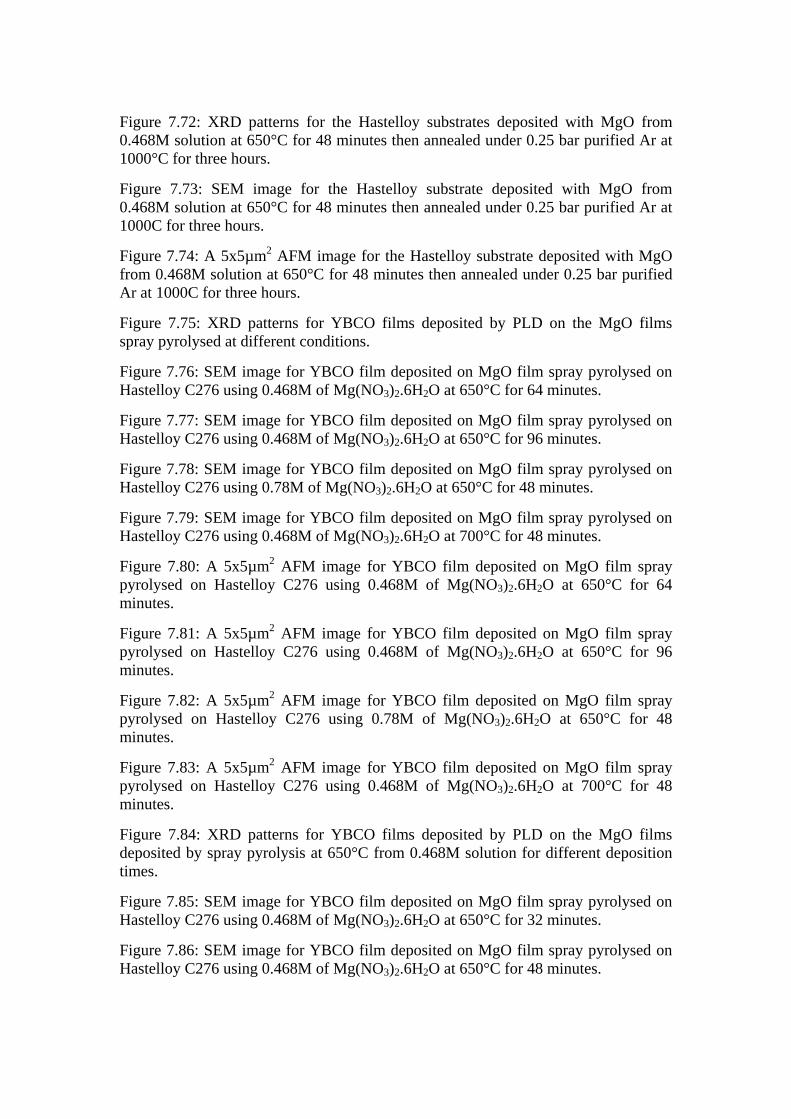
Figure 7.72: XRD patterns for the Hastelloy substrates deposited with MgO from 0.468M solution at 650°C for 48 minutes then annealed under 0.25 bar purified Ar at 1000°C for three hours.
Figure 7.73: SEM image for the Hastelloy substrate deposited with MgO from 0.468M solution at 650°C for 48 minutes then annealed under 0.25 bar purified Ar at 1000C for three hours.
Figure 7.74: A 5x5µm2 AFM image for the Hastelloy substrate deposited with MgO from 0.468M solution at 650°C for 48 minutes then annealed under 0.25 bar purified Ar at 1000C for three hours.
Figure 7.75: XRD patterns for YBCO films deposited by PLD on the MgO films spray pyrolysed at different conditions.
Figure 7.76: SEM image for YBCO film deposited on MgO film spray pyrolysed on Hastelloy C276 using 0.468M of Mg(NO3)2.6H2O at 650°C for 64 minutes.
Figure 7.77: SEM image for YBCO film deposited on MgO film spray pyrolysed on Hastelloy C276 using 0.468M of Mg(NO3)2.6H2O at 650°C for 96 minutes.
Figure 7.78: SEM image for YBCO film deposited on MgO film spray pyrolysed on Hastelloy C276 using 0.78M of Mg(NO3)2.6H2O at 650°C for 48 minutes.
Figure 7.79: SEM image for YBCO film deposited on MgO film spray pyrolysed on Hastelloy C276 using 0.468M of Mg(NO3)2.6H2O at 700°C for 48 minutes.
Figure 7.80: A 5x5µm2 AFM image for YBCO film deposited on MgO film spray pyrolysed on Hastelloy C276 using 0.468M of Mg(NO3)2.6H2O at 650°C for 64 minutes.
Figure 7.81: A 5x5µm2 AFM image for YBCO film deposited on MgO film spray pyrolysed on Hastelloy C276 using 0.468M of Mg(NO3)2.6H2O at 650°C for 96 minutes.
Figure 7.82: A 5x5µm2 AFM image for YBCO film deposited on MgO film spray pyrolysed on Hastelloy C276 using 0.78M of Mg(NO3)2.6H2O at 650°C for 48 minutes.
Figure 7.83: A 5x5µm2 AFM image for YBCO film deposited on MgO film spray pyrolysed on Hastelloy C276 using 0.468M of Mg(NO3)2.6H2O at 700°C for 48 minutes.
Figure 7.84: XRD patterns for YBCO films deposited by PLD on the MgO films deposited by spray pyrolysis at 650°C from 0.468M solution for different deposition times.
Figure 7.85: SEM image for YBCO film deposited on MgO film spray pyrolysed on Hastelloy C276 using 0.468M of Mg(NO3)2.6H2O at 650°C for 32 minutes.
Figure 7.86: SEM image for YBCO film deposited on MgO film spray pyrolysed on Hastelloy C276 using 0.468M of Mg(NO3)2.6H2O at 650°C for 48 minutes.

Figure 7.87: A 5x5µm2 AFM image for YBCO film deposited on MgO film spray pyrolysed on Hastelloy C276 using 0.468M of Mg(NO3)2.6H2O at 650°C for 32 minutes.
Figure 7.88: A 5x5µm2 AFM image for YBCO film deposited on MgO film spray pyrolysed on Hastelloy C276 using 0.468M of Mg(NO3)2.6H2O at 650°C for 48 minutes.
Figure 7.89: : (001) X-ray pole figure showing YBCO {006} planes, at 2θ of 46.65°, for YBCO film deposited by PLD on Hastelloy substrate buffered with MgO deposited by spray pyrolysis at 650oC from the nitrate precursor using 0.468M concentration for 48 minutes.
Figure 7.90: EBSD pattern showing the {006} planes for YBCO film deposited by PLD on Hastelloy substrate buffered with MgO deposited by spray pyrolysis at 650oC from the nitrate precursor using 0.468M concentration for 48 minutes.
Figure 7.91: AC susceptibility measurement for YBCO deposited at 780οC on the MgO buffer layer deposited by spray pyrolysis at 650οC at different times using 0.468M Mg(NO3)2.6H2O.
Figure 7.92: XRD patterns for MgO deposited by PLD on bare Hastelloy C276 under different energy fluencies.
Figure 7.93: A unit cell for the fluorite crystal structure [267].
Figure 7.94: XRD patterns for CeO2 films deposited by PLD at different conditions on the MgO films spray pyrolysed at 650°C from 0.468M for 48 minutes.
Figure 7.95: SEM image for CeO2 film deposited by PLD at 710°C using 2x10⁻⁴ mbar O2 on the MgO film deposited by spray pyrolysis at 650°C from 0.468M for 48 minutes.
Figure 7.96: SEM image for CeO2 film deposited by PLD at 780°C using 0.6 mbar O2 on the MgO film deposited by spray pyrolysis at 650°C from 0.468M for 48 minutes.
Figure 7.97: A 5x5µm2 AFM image for CeO2 film deposited by PLD at 710°C using 2x10⁻⁴ mbar O2 on the MgO film spray pyrolysed at 650°C from 0.468M for 48 minutes.
Figure 7.98: A 5x5µm2 AFM image for CeO2 film deposited by PLD at 780°C using 0.6 mbar O2 on the MgO film spray pyrolysed at 650°C from 0.468M for 48 minutes.
Figure 7.99: XRD patterns for YBCO and CeO2 films deposited by PLD at different conditions on the MgO films spray pyrolysed at 650°C from 0.468M for 48 minutes.
Figure 7.100: SEM image for YBCO on CeO2 film deposited by PLD at 710°C using 2x10⁻⁴ mbar O2 on the MgO film spray pyrolysed at 650°C from 0.468M for 48 minutes.
Figure 7.101: SEM image for YBCO on CeO2 film deposited by PLD at 780°C using 0.6 mbar O2 on the MgO film spray pyrolysed at 650°C from 0.468M for 48 minutes.

Figure 7.102: A 5x5µm2 AFM image for YBCO on CeO2 film deposited by PLD at 710°C using 2x10⁻⁴ mbar O2 on the MgO film spray pyrolysed at 650°C from 0.468M for 48 minutes.
Figure 7.103: A 5x5µm2 AFM image for YBCO on CeO2 film deposited by PLD at 780°C using 0.6 mbar O2 on the MgO film spray pyrolysed at 650°C from 0.468M for 48 minutes.
Figure 7.104: Cross sectional SEM image for YBCO on CeO2 film deposited by PLD at 780°C using 0.6 mbar O2 on the MgO film spray pyrolysed at 650°C from 0.468M for 48 minutes.
Figure 7.105: (001) X-ray pole figure showing the YBCO {006} planes, at 2θ of 46.65°, for YBCO deposited on CeO2 film which was deposited by PLD at 780°C using 0.6 mbar O2 on the MgO film deposited by spray pyrolysis at 650°C from 0.468M for 48 minutes.
Figure 8.1: TG curve for Mg(CH3COO)2.4H2O.
Figure 8.2: XRD patterns for MgO deposition on Hastelloy C276 using 0.093M of Mg(CH3COO)2.4H2O at different temperatures for 32 minutes.
Figure 8.3: EDX spectrum, using an accelerating voltage of 4KV, for MgO with 0.093M at 500°C with a deposition time of 32 minutes.
Figure 8.4: SEM image for the MgO film deposited on Hastelloy C276 using 0.093M of Mg(CH3COO)2.4H2O at 500°C for 32 minutes.
Figure 8.5: SEM image for the MgO film deposited on Hastelloy C276 using 0.093M of Mg(CH3COO)2.4H2O at 550°C for 32 minutes.
Figure 8.6: SEM image for the MgO film deposited on Hastelloy C276 using 0.093M of Mg(CH3COO)2.4H2O at 600°C for 32 minutes.
Figure 8.7: SEM image for the MgO film deposited on Hastelloy C276 using 0.093M of Mg(CH3COO)2.4H2O at 650°C for 32 minutes.
Figure 8.8: The effect of deposition temperature on MgO film roughness for the films deposited from 0.093M Mg(CH3COO)2.4H2O for 32 minutes.
Figure 8.9: A 5x5µm2 AFM image for the MgO film deposited on Hastelloy C276 using 0.093M of Mg(CH3COO)2.4H2O at 550°C for 32 minutes.
Figure 8.10: AFM section profile image for the MgO film deposited on Hastelloy C276 using 0.093M of Mg(CH3COO)2.4H2O at 550°C for 32 minutes.
Figure 8.11: EDX spectrum, using an accelerating voltage of 4KV, for MgO film deposited with 0.093M solution at 600°C for a deposition time of 32 minutes.
Figure 8.12: (200) X-ray pole figure, at 2θ of 43.12°, of the MgO film deposited at 600°C from a solution of 0.093M for 32 minutes.
Figure 8.13: (200) X-ray pole figure, at 2θ of 43.12°, of the MgO film deposited at 650°C from a solution of 0.093M for 32 minutes.

Figure 8.14: X-ray diffraction ω−scan for the film deposited at 600°C from 0.093M solution showing MgO (200) with a FWHM of 18.7ο.
Figure 8.15: X-ray diffraction ω−scan for the film deposited at 650°C from 0.093M solution showing MgO (200) with a FWHM of 17.67ο.
Figure 8.16: XRD patterns for MgO deposition on Hastelloy C276 using 0.093M of Mg(CH3COO)2.4H2O at different temperatures and times.
Figure 8.17: SEM image for the MgO film deposited on Hastelloy C276 using 0.093M of Mg(CH3COO)2.4H2O at 550°C for 64 minutes.
Figure 8.18: SEM image for the MgO film deposited on Hastelloy C276 using 0.093M of Mg(CH3COO)2.4H2O at 600°C for 64 minutes.
Figure 8.19: A 5x5µm2 AFM image for the MgO film deposited on Hastelloy C276 using 0.093M of Mg(CH3COO)2.4H2O at 550°C for 64 minutes.
Figure 8.20: A 5x5µm2 AFM image for the MgO film deposited on Hastelloy C276 using 0.093M of Mg(CH3COO)2.4H2O at 600°C for 64 minutes.
Figure 8.21: XRD patterns for MgO deposition on Hastelloy C276 showing the double deposition effect using 0.093M Mg(CH3COO)2.4H2O at 600°C for 32 minutes.
Figure 8.22: SEM image for MgO on Hastelloy C276 with the double deposition using 0.093M Mg(CH3COO)2.4H2O at 600°C for 32 minutes.
Figure 8.23: A 5x5µm2 AFM image for MgO on Hastelloy C276 with the double deposition using 0.093M Mg(CH3COO)2.4H2O at 600°C for 32 minutes.
Figure 8.24: XRD patterns for MgO deposition on Hastelloy C276 at 600°C for 32 minutes using different concentrations of Mg(CH3COO)2.4H2O.
Figure 8.25: SEM image for MgO deposition on Hastelloy C276 at 600°C for 32 minutes using 0.14M Mg(CH3COO)2.4H2O.
Figure 8.26: SEM image for MgO deposition on Hastelloy C276 at 600°C for 32 minutes using 0.279M Mg(CH3COO)2.4H2O.
Figure 8.27: A 5x5µm2 AFM image for MgO deposition on Hastelloy C276 at 600°C for 32 minutes using 0.14M Mg(CH3COO)2.4H2O.
Figure 8.28: A 5x5µm2 AFM image for MgO deposition on Hastelloy C276 at 600°C for 32 minutes using 0.279M Mg(CH3COO)2.4H2O.
Figure 8.29: XPS spectrum for the MgO thin film deposited on Hastelloy C276 substrates using 0.093M Mg(CH3COO)2.4H2O at 550οC showing the Mg 2P.
Figure 8.30: XPS spectrum for the MgO thin film deposited on Hastelloy C276 substrates using 0.093M Mg(CH3COO)2.4H2O at 550οC showing the O 1S.
Figure 8.31: XPS spectrum for the MgO thin film deposited on Hastelloy C276 substrates using 0.093M Mg(CH3COO)2.4H2O at 600οC for 32 min. showing the Mg 2P.

Figure 8.32: XPS spectrum for the MgO thin film deposited on Hastelloy C276 substrates using 0.093M Mg(CH3COO)2.4H2O at 600οC for 32 min. showing the O 1S.
Figure 8.33: XRD patterns for MgO deposition on Hastelloy C276 using 0.093M Mg(CH3COO)2.4H2O at 600°C for 32 minutes and at different inclination angles.
Figure 8.34: The effect of inclination angle on the film roughness of MgO film deposited from 0.093M solution at 600°C for 32 minutes.
Figure 8.35: SEM image for MgO deposition on Hastelloy C276 using 0.093M Mg(CH3COO)2.4H2O at 600°C for 32 minutes at 20°.
Figure 8.36: SEM image for MgO deposition on Hastelloy C276 using 0.093M Mg(CH3COO)2.4H2O at 600°C for 32 minutes at 45°.
Figure 8.37: SEM image for MgO deposition on Hastelloy C276 using 0.093M Mg(CH3COO)2.4H2O at 600°C for 32 minutes at 60°.
Figure 8.38: XRD patterns for MgO deposition on Hastelloy C276 using 0.093M Mg(CH3COO)2.4H2O at 600°C for 32 minutes and at different Ar flow rates.
Figure 8.39: SEM image for the Hastelloy C276 deposited with MgO using 0.093M solution at 600°C for 32 minutes and using an Ar flow rate of 5 l/min.
Figure 8.40: SEM image for the Hastelloy C276 deposited with MgO using 0.093M solution at 600°C for 32 minutes and using an Ar flow rate of 15 l/min.
Figure 8.41: The effect of Ar flow rate on the roughness of MgO films deposited from 0.093M solution at 600°C for 32 minutes.
Figure 8.42: XRD patterns for the Hastelloy substrates deposited with MgO from 0.093M at 600°C for 32 minutes after O2 anneal at different temperatures and times.
Figure 8.43: XRD patterns with a narrow scan for the Hastelloy substrates deposited with MgO from 0.093M at 600°C for 32 minutes after O2 anneal at different temperatures and times.
Figure 8.44 SEM image for the Hastelloy substrate deposited with MgO at 600°C for 32 minutes from 0.093M solution then annealed at 800°C under O2 for three hours.
Figure 8.45 SEM image for the Hastelloy substrate deposited with MgO at 600°C for 32 minutes from 0.093M solution then annealed at 1000°C under O2 for three hours.
Figure 8.46: A 5x5µm2 AFM image for the Hastelloy substrate deposited with MgO at 600°C for 32 minutes from 0.093M solution then annealed at 800°C under O2 for three hours.
Figure 8.47: A 5x5µm2 AFM image for the Hastelloy substrate deposited with MgO at 600°C for 32 minutes from 0.093M solution then annealed at 1000°C under O2 for three hours.
Figure 8.48: SEM image for a bare Hastelloy C276 substrate annealed at 800°C under O2 for three hours.
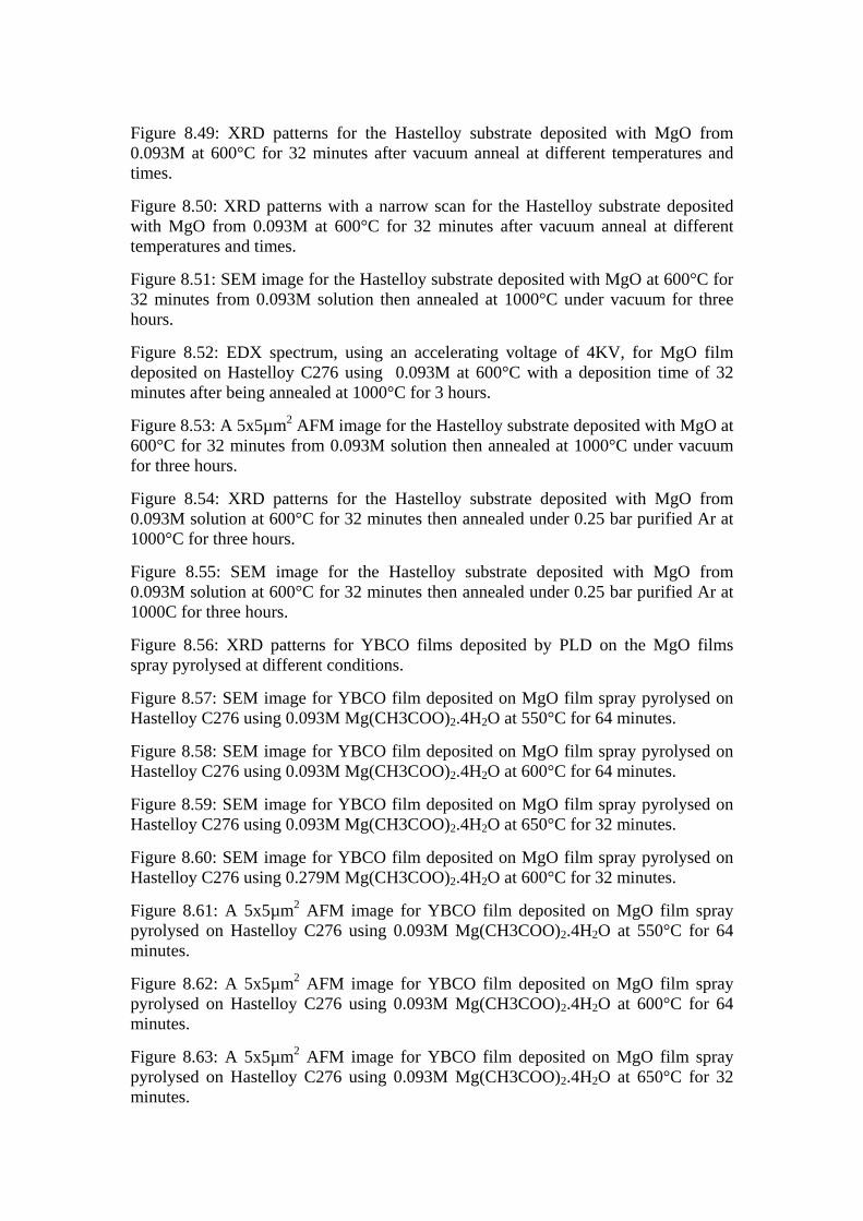
Figure 8.49: XRD patterns for the Hastelloy substrate deposited with MgO from 0.093M at 600°C for 32 minutes after vacuum anneal at different temperatures and times.
Figure 8.50: XRD patterns with a narrow scan for the Hastelloy substrate deposited with MgO from 0.093M at 600°C for 32 minutes after vacuum anneal at different temperatures and times.
Figure 8.51: SEM image for the Hastelloy substrate deposited with MgO at 600°C for 32 minutes from 0.093M solution then annealed at 1000°C under vacuum for three hours.
Figure 8.52: EDX spectrum, using an accelerating voltage of 4KV, for MgO film deposited on Hastelloy C276 using 0.093M at 600°C with a deposition time of 32 minutes after being annealed at 1000°C for 3 hours.
Figure 8.53: A 5x5µm2 AFM image for the Hastelloy substrate deposited with MgO at 600°C for 32 minutes from 0.093M solution then annealed at 1000°C under vacuum for three hours.
Figure 8.54: XRD patterns for the Hastelloy substrate deposited with MgO from 0.093M solution at 600°C for 32 minutes then annealed under 0.25 bar purified Ar at 1000°C for three hours.
Figure 8.55: SEM image for the Hastelloy substrate deposited with MgO from 0.093M solution at 600°C for 32 minutes then annealed under 0.25 bar purified Ar at 1000C for three hours.
Figure 8.56: XRD patterns for YBCO films deposited by PLD on the MgO films spray pyrolysed at different conditions.
Figure 8.57: SEM image for YBCO film deposited on MgO film spray pyrolysed on Hastelloy C276 using 0.093M Mg(CH3COO)2.4H2O at 550°C for 64 minutes.
Figure 8.58: SEM image for YBCO film deposited on MgO film spray pyrolysed on Hastelloy C276 using 0.093M Mg(CH3COO)2.4H2O at 600°C for 64 minutes.
Figure 8.59: SEM image for YBCO film deposited on MgO film spray pyrolysed on Hastelloy C276 using 0.093M Mg(CH3COO)2.4H2O at 650°C for 32 minutes.
Figure 8.60: SEM image for YBCO film deposited on MgO film spray pyrolysed on Hastelloy C276 using 0.279M Mg(CH3COO)2.4H2O at 600°C for 32 minutes.
Figure 8.61: A 5x5µm2 AFM image for YBCO film deposited on MgO film spray pyrolysed on Hastelloy C276 using 0.093M Mg(CH3COO)2.4H2O at 550°C for 64 minutes.
Figure 8.62: A 5x5µm2 AFM image for YBCO film deposited on MgO film spray pyrolysed on Hastelloy C276 using 0.093M Mg(CH3COO)2.4H2O at 600°C for 64 minutes.
Figure 8.63: A 5x5µm2 AFM image for YBCO film deposited on MgO film spray pyrolysed on Hastelloy C276 using 0.093M Mg(CH3COO)2.4H2O at 650°C for 32 minutes.
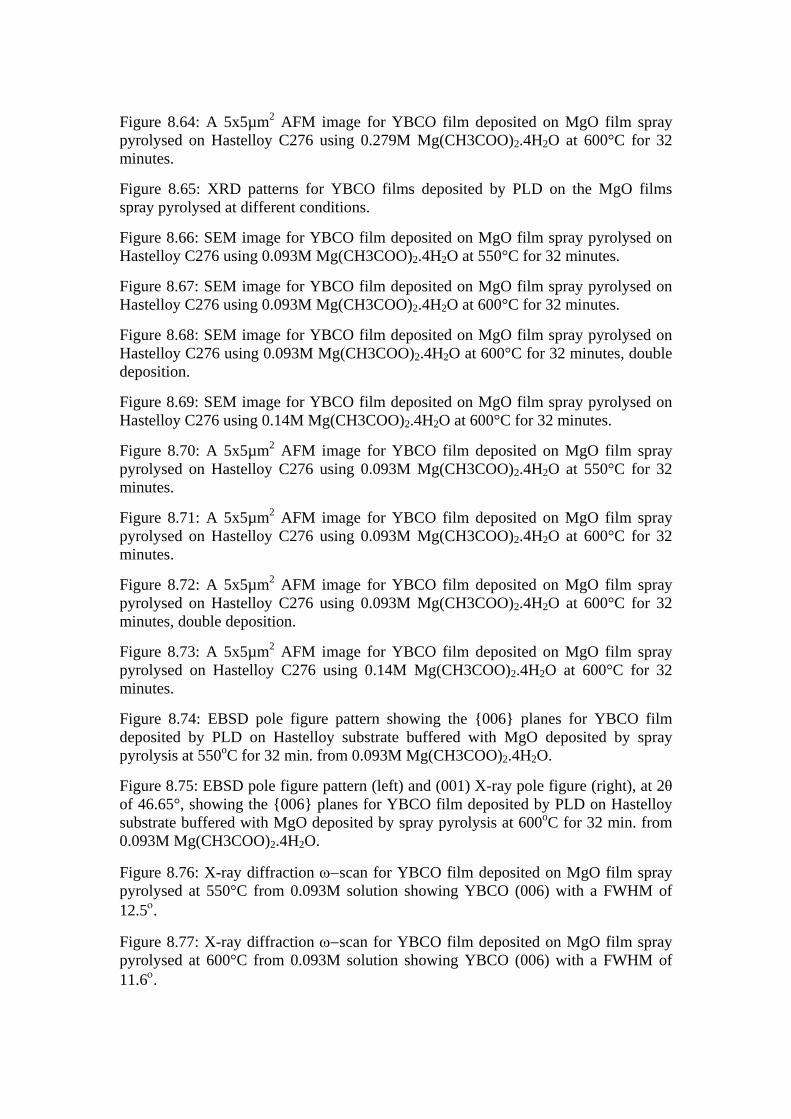
Figure 8.64: A 5x5µm2 AFM image for YBCO film deposited on MgO film spray pyrolysed on Hastelloy C276 using 0.279M Mg(CH3COO)2.4H2O at 600°C for 32 minutes.
Figure 8.65: XRD patterns for YBCO films deposited by PLD on the MgO films spray pyrolysed at different conditions.
Figure 8.66: SEM image for YBCO film deposited on MgO film spray pyrolysed on Hastelloy C276 using 0.093M Mg(CH3COO)2.4H2O at 550°C for 32 minutes.
Figure 8.67: SEM image for YBCO film deposited on MgO film spray pyrolysed on Hastelloy C276 using 0.093M Mg(CH3COO)2.4H2O at 600°C for 32 minutes.
Figure 8.68: SEM image for YBCO film deposited on MgO film spray pyrolysed on Hastelloy C276 using 0.093M Mg(CH3COO)2.4H2O at 600°C for 32 minutes, double deposition.
Figure 8.69: SEM image for YBCO film deposited on MgO film spray pyrolysed on Hastelloy C276 using 0.14M Mg(CH3COO)2.4H2O at 600°C for 32 minutes.
Figure 8.70: A 5x5µm2 AFM image for YBCO film deposited on MgO film spray pyrolysed on Hastelloy C276 using 0.093M Mg(CH3COO)2.4H2O at 550°C for 32 minutes.
Figure 8.71: A 5x5µm2 AFM image for YBCO film deposited on MgO film spray pyrolysed on Hastelloy C276 using 0.093M Mg(CH3COO)2.4H2O at 600°C for 32 minutes.
Figure 8.72: A 5x5µm2 AFM image for YBCO film deposited on MgO film spray pyrolysed on Hastelloy C276 using 0.093M Mg(CH3COO)2.4H2O at 600°C for 32 minutes, double deposition.
Figure 8.73: A 5x5µm2 AFM image for YBCO film deposited on MgO film spray pyrolysed on Hastelloy C276 using 0.14M Mg(CH3COO)2.4H2O at 600°C for 32 minutes.
Figure 8.74: EBSD pole figure pattern showing the {006} planes for YBCO film deposited by PLD on Hastelloy substrate buffered with MgO deposited by spray pyrolysis at 550oC for 32 min. from 0.093M Mg(CH3COO)2.4H2O.
Figure 8.75: EBSD pole figure pattern (left) and (001) X-ray pole figure (right), at 2θ of 46.65°, showing the {006} planes for YBCO film deposited by PLD on Hastelloy substrate buffered with MgO deposited by spray pyrolysis at 600oC for 32 min. from 0.093M Mg(CH3COO)2.4H2O.
Figure 8.76: X-ray diffraction ω−scan for YBCO film deposited on MgO film spray pyrolysed at 550°C from 0.093M solution showing YBCO (006) with a FWHM of 12.5ο.
Figure 8.77: X-ray diffraction ω−scan for YBCO film deposited on MgO film spray pyrolysed at 600°C from 0.093M solution showing YBCO (006) with a FWHM of 11.6ο.

Figure 8.78: X-ray diffraction φ−scan for YBCO film deposited on MgO film spray pyrolysed at 600°C from 0.093M solution showing YBCO (013) with a FWHM of about 40ο.
Figure 8.79: EBSD histogram showing grain misorientation angles for YBCO film deposited on MgO film spray pyrolysed on Hastelloy C276 using 0.093M Mg(CH3COO)2.4H2O at 550°C for 32 minutes.
Figure 8.80: EBSD histogram showing grain misorientation angles for YBCO film deposited on MgO film spray pyrolysed on Hastelloy C276 using 0.093M Mg(CH3COO)2.4H2O at 600°C for 32 minutes.
Figure 8.81: Cross sectional SEM image of YBCO film deposited on MgO film spray pyrolysed on Hastelloy C276 using 0.093M Mg(CH3COO)2.4H2O at 600°C for 32 minutes.
Figure 8.82: EDX line scan using 20KV of YBCO film deposited on MgO film spray pyrolysed on Hastelloy C276 using 0.093M Mg(CH3COO)2.4H2O at 600°C for 32 minutes.
Figure 8.83: AC susceptibility measurement for YBCO deposited at 780οC on the MgO buffer layer spray pyrolysed at different conditions.
Figure 8.84: XPS spectrum for the MgO thin film deposited on Hastelloy C276 substrate using 0.093M Mg(CH3COO)2.4H2O at 600οC for 32 min. showing the C 1s.
Figure 8.85: XRD patterns for CeO2 films deposited by PLD at different conditions on the MgO films spray pyrolysed at 600°C from 0.093M for 32 minutes.
Figure 8.86: SEM image for CeO2 film deposited by PLD at 710°C using 2x10⁻⁴ mbar O2 on the MgO film deposited by spray pyrolysis at 600°C from 0.093M for 32 minutes.
Figure 8.87: SEM image for CeO2 film deposited by PLD at 780°C using 0.6 mbar O2 on the MgO film deposited by spray pyrolysis at 600°C from 0.093M for 32 minutes.
Figure 8.88: A 5x5µm2 AFM image for CeO2 film deposited by PLD at 710°C using 2x10⁻⁴ mbar O2 on the MgO film deposited by spray pyrolysis at 600°C from 0.093M for 32 minutes.
Figure 8.89: A 5x5µm2 AFM image for CeO2 film deposited by PLD at 780°C using 0.6 mbar O2 on the MgO film deposited by spray pyrolysis at 600°C from 0.093M for 32 minutes.
Figure 8.90: XRD patterns for YBCO and CeO2 films deposited by PLD at different conditions on the MgO films deposited by spray pyrolysis at 600°C from 0.093M for 32 minutes.
Figure 8.91: SEM image for YBCO on CeO2 film deposited by PLD at 710°C using 2x10⁻⁴ mbar O2 on the MgO film deposited by spray pyrolysis at 600°C from 0.093M for 32 minutes.
Figure 8.92: SEM image for YBCO on CeO2 film deposited by PLD at 780°C using 0.6 mbar O2 on the MgO film deposited by spray pyrolysis at 600°C from 0.093M for 32 minutes.

Figure 8.93: A 5x5µm2 AFM image for YBCO on CeO2 film deposited by PLD at 710°C using 2x10⁻⁴ mbar O2 on the MgO film deposited by spray pyrolysis at 600°C from 0.093M for 32 minutes.
Figure 8.94: A 5x5µm2 AFM image for YBCO on CeO2 film deposited by PLD at 780°C using 0.6 mbar O2 on the MgO film deposited by spray pyrolysis at 600°C from 0.093M for 32 minutes.
Figure 8.95: AC susceptibility measurement for YBCO deposited on CeO2 film deposited by PLD at 780°C using 0.6 mbar O2 on the MgO film deposited by spray pyrolysis at 600°C from 0.093M for 32 minutes.
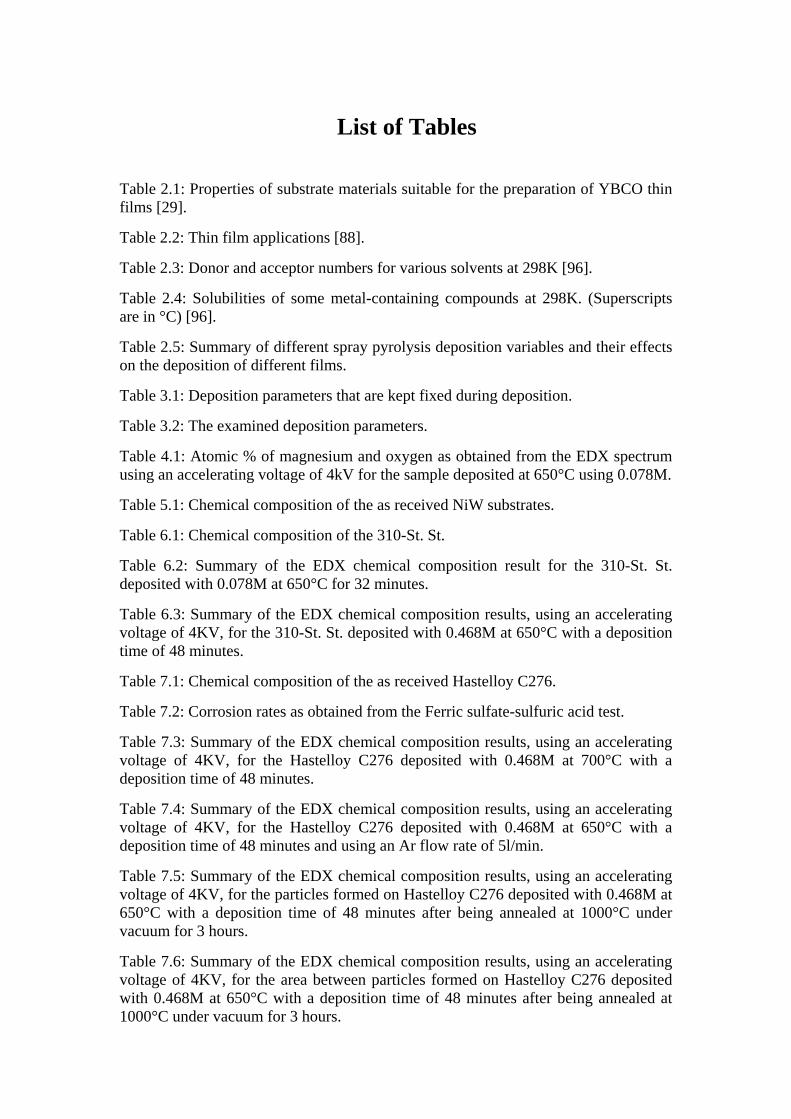
List of Tables
Table 2.1: Properties of substrate materials suitable for the preparation of YBCO thin films [29].
Table 2.2: Thin film applications [88].
Table 2.3: Donor and acceptor numbers for various solvents at 298K [96].
Table 2.4: Solubilities of some metal-containing compounds at 298K. (Superscripts are in °C) [96].
Table 2.5: Summary of different spray pyrolysis deposition variables and their effects on the deposition of different films.
Table 3.1: Deposition parameters that are kept fixed during deposition.
Table 3.2: The examined deposition parameters.
Table 4.1: Atomic % of magnesium and oxygen as obtained from the EDX spectrum using an accelerating voltage of 4kV for the sample deposited at 650°C using 0.078M.
Table 5.1: Chemical composition of the as received NiW substrates.
Table 6.1: Chemical composition of the 310-St. St.
Table 6.2: Summary of the EDX chemical composition result for the 310-St. St. deposited with 0.078M at 650°C for 32 minutes.
Table 6.3: Summary of the EDX chemical composition results, using an accelerating voltage of 4KV, for the 310-St. St. deposited with 0.468M at 650°C with a deposition time of 48 minutes.
Table 7.1: Chemical composition of the as received Hastelloy C276.
Table 7.2: Corrosion rates as obtained from the Ferric sulfate-sulfuric acid test.
Table 7.3: Summary of the EDX chemical composition results, using an accelerating voltage of 4KV, for the Hastelloy C276 deposited with 0.468M at 700°C with a deposition time of 48 minutes.
Table 7.4: Summary of the EDX chemical composition results, using an accelerating voltage of 4KV, for the Hastelloy C276 deposited with 0.468M at 650°C with a deposition time of 48 minutes and using an Ar flow rate of 5l/min.
Table 7.5: Summary of the EDX chemical composition results, using an accelerating voltage of 4KV, for the particles formed on Hastelloy C276 deposited with 0.468M at 650°C with a deposition time of 48 minutes after being annealed at 1000°C under vacuum for 3 hours.
Table 7.6: Summary of the EDX chemical composition results, using an accelerating voltage of 4KV, for the area between particles formed on Hastelloy C276 deposited with 0.468M at 650°C with a deposition time of 48 minutes after being annealed at 1000°C under vacuum for 3 hours.

Table 7.7: Summary of the EDX chemical composition results (using an accelerating voltage of 4KV) of the as received MgO single crystal.
Table 7.8: Summary of the EDX chemical composition results (using an accelerating voltage of 4KV) of the as received MgO single crystal after vacuum anneal at 1000°C for 3 hours.
Table 8.1: Summary of the EDX chemical composition results, using an accelerating voltage of 4KV, for MgO with 0.093M at 500°C with a deposition time of 32 minutes.
Table 8.2: Summary of the EDX chemical composition results, using an accelerating voltage of 4KV, for MgO film deposited with 0.093M at 600°C for a deposition time of 32 minutes.
Table 8.3: Summary of the EDX chemical composition results, using an accelerating voltage of 4KV, for MgO film deposited on Hastelloy C276 using 0.093M at 600°C with a deposition time of 32 minutes after being annealed at 1000°C for 3 hours.
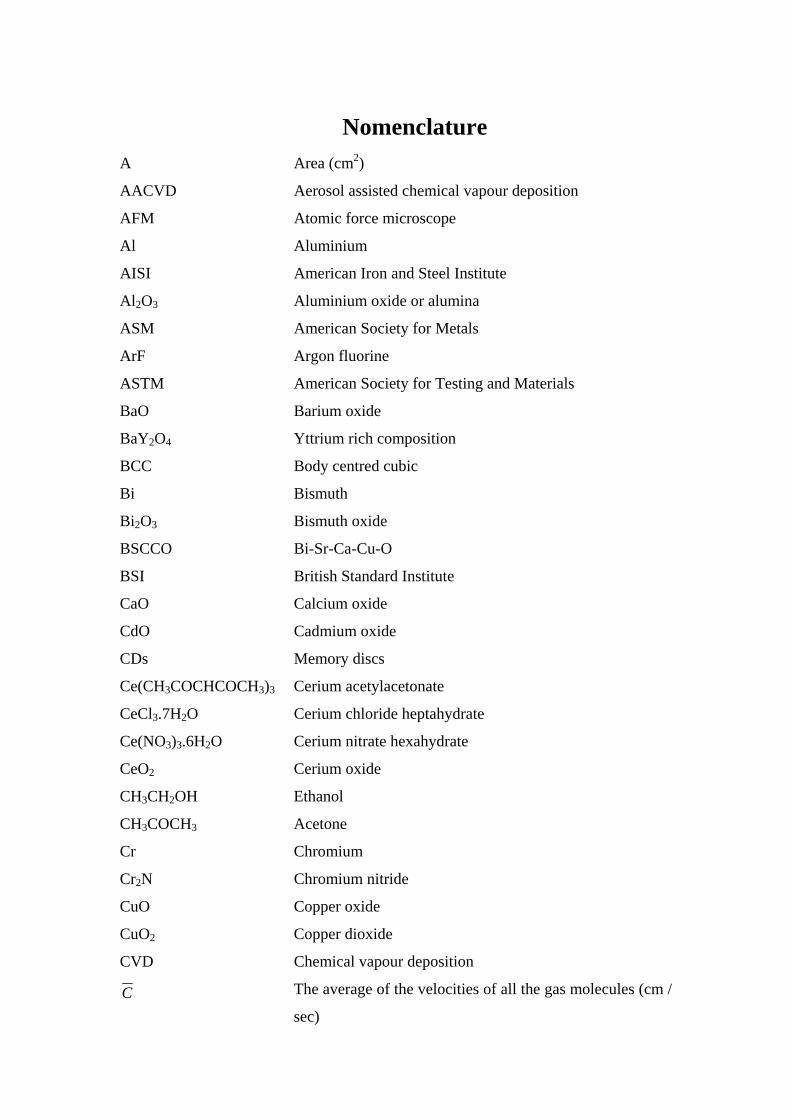
Nomenclature A Area (cm2)
AACVD Aerosol assisted chemical vapour deposition
AFM Atomic force microscope
Al Aluminium
AISI American Iron and Steel Institute
Al2O3 Aluminium oxide or alumina
ASM American Society for Metals
ArF Argon fluorine
ASTM American Society for Testing and Materials
BaO Barium oxide
BaY2O4 Yttrium rich composition
BCC Body centred cubic
Bi Bismuth
Bi2O3 Bismuth oxide
BSCCO Bi-Sr-Ca-Cu-O
BSI British Standard Institute
CaO Calcium oxide
CdO Cadmium oxide
CDs Memory discs
Ce(CH3COCHCOCH3)3 Cerium acetylacetonate
CeCl3.7H2O Cerium chloride heptahydrate
Ce(NO3)3.6H2O Cerium nitrate hexahydrate
CeO2 Cerium oxide
CH3CH2OH Ethanol
CH3COCH3 Acetone
Cr Chromium
Cr2N Chromium nitride
CuO Copper oxide
CuO2 Copper dioxide
CVD Chemical vapour deposition
C The average of the velocities of all the gas molecules (cm /
sec)

D The diffusivity of the gas or vapour (diffusion coefficient)
(cm2/sec)
d The interplanar spacing (nm)
dp Particle or droplet diameter (cm)
dpo The initial particle diameter (cm)
EB The electron binding energy (Joules)
EBSD Electron backscattered diffraction
EDS Energy dispersive spectroscopy
EK The kinetic energy of the ejected photo-electron (Joules)
ESAVD Electrostatic spray-assisted vapour deposition
F1 Correction factor
F2 Correction factor
FCC Face centred cubic
Fe2(SO4)3.9H2O iron (III) sulfate nonahydrate
FWHM Full width half maximum
tf Transducer frequency (Hz)
H The magnetic field strength (Amp./m), differentiated from
Henry’s constant from context
H Henry’s constant which relates the concentration in the
liquid to the partial pressure in the gas (L.atm/mole)
h Plank’s constant (6.626 × 10⁻³⁴ Joule.second)
H2C2O4 Oxalic acid
HBE Higher binding energy
Hc Critical magnetic field (Tesla)
Hc1 Lower critical field (Tesla)
Hc2 Upper critical field (Tesla)
He Helium
HF Hydrofluoric acid
Hg Mercury
HTS high temperature superconductor
HTSCs high temperature superconductors
hυ The incident photon energy (Joules)
In2O3 Indium oxide

IBAD Ion beam assisted deposition
InC13 Indium chloride
IGC Intergranular corrosion
ISD Inclined substrate deposition
ISO International organisation for standardisation
Jc Critical current density (MA/cm2)
K Constant and its value depends on the corrosion rate unit,
ex. 3.45x10⁻⁶ if the corrosion rate is in mm/yr
k Spring constant (N/m)
kB Boltzmann’s constant (erg/molecule. K)
Kn Knudsen number, dimensionless
ks The surface reaction rate constant (cm/sec)
k v Reaction rate constant
LaAlO3 Lanthanum aluminium oxide
LaB6 Lanthanum boride
LAO LaAlO3
LBCO La-Ba-Cu-O
M Molecular weight (g/mole) or molarity (mole/l) or the
magnetization of the material (the magnetic dipole
moment per unit volume) (Amp/m) depending on context.
m1 The mass of transported molecule or atom in the particle
(g)
MCA Multichannel analyzer
Me3PO Trimethylphosphine oxide
Mg(CH3COCHCOCH3)3 Magnesium acetylacetonate
Mg(CH3COO)2.4H2O Magnesium acetate tetrahydrate
Mg(NO)3.6H2O Magnesium nitrate hexahydrate
MgB2 Magnesium diboride
MgCO3 Magnesium carbonate
MgO Magnesium oxide
Mg(OH)2 Magnesium hydroxide
N The number of points within a given area.
n Order of diffraction
NA Avogadro’s number (6.023x10²³ molecules/mole)
NaCl Sodium chloride
Nb Niobium
Nb3Ge Niobium-germanium intermetallic compound
Ni Nickel
NMR Nuclear magnetic resonance
NiW Nickel-tungsten intermetallic compound
N ∞ Droplet concentration per unit volume (number/cm3)
p1 Partial pressure of the vapour for species 1 far from the
particle (dyne/cm2)
p1s The reactant partial pressure at the particle surface
(dyne/cm2)
pd Partial pressure at the particle surface (dyne/cm2)
pe The vapour pressure over a flat surface (dyne/cm2)
PLD Pulsed laser deposition
PVD Physical vapour deposition
RABiTS Rolling assisted biaxially textured substrates
RMS Root mean square
r v The rate of reaction per unit volume (moles/cm3 sec)
SbCl5 Antimony pentachloride
SEM Scanning electron microscopy
Si Silicon
SiO2 Silicon oxide
SnCl2 Tin chloride (stannous chloride)
SND substrate-nozzle distance
SnO2 Tin oxide
SPM Scanning probe microscopy
SrCO3 Strontium carbonate
SrTiO3 Strontium titanate
STM scanning tunnelling microscopy
STO SrTiO3
T Temperature (K or °C)
t Time (second or hours)

Tc Transition or critical temperature (K or °C)
TEM Transmission electron microscopy
TGA Thermogravimetrical analysis
TiN Titanium nitride
Tl Thallium
WDS Wavelength dispersive spectroscopy
WEDM Wire electric discharge machine
WQ Water quench
x Oxygen deficiency or cantilever deflection (m) depending
on context.
XPS X-ray photoelectron spectroscopy
XRD X-ray diffraction
χ/ Real susceptibility (dimensionless)
χ// Imaginary susceptibility (dimensionless)
Y Yttrium
Y2O3 Yttria (yttrium oxide)
YBCO Y-BA-Cu-O
YBCO-123 YBa2Cu3O7-x
YSZ Yttria stabilised zirconia
Z Vertical position of the scanner
Zave The average Z value within the given area
Zi The current Z value
Zn(CH3CO2)2.2H2O Zinc acetate dihydrate
ZnO Zinc oxide
Greek αs Sticking coefficient (dimensionless)
θ The Bragg angle, the angle between the incident X-ray
beam and the particular crystal plane under consideration
λ Wavelength of an incident monochromatic X-ray beam
(nm) or mean free path of a gas (cm) depending on the
context
µ Viscosity (g/cm sec)
ν Particle volume (cm3)
ν1 Volume of transported molecule or atom in the particle or
volume of the reaction products (cm3) depending on the
context
υ Frequency (Hz)
ρ Density (g/cm3)
ρ1 Density of the material in the particle in the solid or liquid
state (g/cm3)
ρ p Particle density (g/cm3)
σ Surface tension (erg/cm2)
τGC Characteristic time for particle growth in continuum
regime (second)
τGF Characteristic time for particle condensation or
evaporation in free molecular regime (second)
τGSR The characteristic time for particle growth by surface
reaction (second)
τsat The time required to saturate the gas with the evaporating
droplets (second)
Δm Mass loss (g)

1
1 Introduction

2
The use of low temperature superconductors (LTS) has many limitations
especially the low temperature refrigeration. Therefore, high temperature
superconductors (HTS), which can be operated in a relatively inexpensive liquid
nitrogen cryostat, have been produced and developed. The first generation of HTS
wires were based on Bi-Sr-Ca-Cu-O (BSCCO) filaments embedded in an Ag alloy.
The superconducting properties of the BSCCO family, however, are limited because
of their intrinsically weak pinning properties in high magnetic fields. Therefore,
YBa2Cu3O7-x (YBCO), the superconducting constituent of the second generation of
HTS tapes, also referred to as coated conductors, is currently of great interest with
regard to producing HTS wires based on flexible coated conductors, consisting of a
layer of YBCO deposited on a thin metallic substrate. The interest in YBCO is
because of its excellent transport properties in high magnetic field, and good
mechanical flexibility. It can be produced with high degree of biaxial texture, has no
high angle grain boundaries, and is easy to prepare single phase YBa2Cu3O7-x under
normal temperature and pressure conditions. Therefore, it is a cost-effective way to
manufacture flexible and high current density wires.
At present the coated conductors are produced by the relatively expensive ion
beam assisted deposition (IBAD), inclined substrate deposition (ISD) and rolling
assisted biaxially textured substrates (RABiTS). The challenge in these is to copy the
texture of the substrate to YBCO through buffer layers.
Spray pyrolysis which is also called droplet deposition involves the deposition
of evaporating droplets containing reactants onto surfaces, followed by further solvent
evaporation and chemical reaction on the surface. It is used for the preparation of thin
metals of noble metals, metal oxides, spinel oxides and superconducting compounds;
because it is a simple, inexpensive, non-vacuum technique and has a high deposition
rate. However, there are not many reports in literature referring to the deposition of
buffer layers, and more specifically no reports for MgO on metallic substrates, by
spray pyrolysis. Besides that, MgO is considered as compatible substrate onto which
HTS (YBCO) can be deposited without a buffer layer and this will be confirmed in
section 4.5.1. Therefore, MgO thin film may exhibit the same property and needs to
be investigated.
The aim of this work is to use spray pyrolysis as the deposition technique for
MgO as a single buffer layer; to reduce the usual multi-layer buffer architecture, on
different substrates using magnesium acetates and magnesium nitrates as precursors.

3
Si single crystals were first used to optimise the deposition parameters. The deposition
was then performed on NiW RABiTS substrates and on oxidised NiW i.e. on (200)
textured NiO grown on NiW. For the purpose of making the process more cost
effective, MgO was also deposited on polycrystalline metallic substrates (310-
austenitic stainless steel and Hastelloy C276). The effects of different deposition
conditions and different annealing treatments on the deposited MgO films on
Hastelloy C276 were investigated. To evaluate the performance of MgO as a buffer
layer, YBCO was subsequently deposited by PLD. This is a well established route to
high quality films, although spray pyrolysis of the YBCO layer should also be a
possibility in the future. In an attempt to control the in-plane texture of YBCO, CeO2
was also deposited by PLD on top of the spray pyrolysed MgO on Hastelloy C276.
The characterization of the deposited thin films (MgO, CeO2 and YBCO) was
done using all or some of the following: SEM, EBSD, XPS, AFM, X-ray diffraction
2θ-scans, rocking curve (ω-scans), phi (φ) scans, and X-ray pole-figure
measurements. The superconducting transition temperatures were measured using AC
susceptibility.
In this work MgO was deposited epitaxially on Si substrates by spray pyrolysis.
However, YBCO deposition by PLD on top of the spray pyrolysed MgO films
resulted in broad superconducting transition temperatures due to the thermal strains in
the deposited MgO films. MgO deposition by spray pyrolysis on 310-austenitic
stainless steel, NiW RABiTS and on textured NiO grown on NiW RABiTS was not
successful because of the substrate and/or NiO oxide layer instabilities under the
spray pyrolysis deposition conditions. MgO deposition on Hastelloy C276 by spray
pyrolysis (see chapter 8 and 9 where most of the work is presented) resulted in weak
MgO (200) peaks when using the nitrate precursor and strong MgO (200) peaks when
using the acetate precursors. Subsequent YBCO deposition by PLD resulted in broad
superconducting transition temperatures due to the weakly textured MgO film when
using the nitrate precursor and due to carbon contamination when using the acetate
precursor. It was also found that MgO film (deposited from the nitrate and acetate
precursors) smoothness on Hastelloy C276 is critical for subsequent YBCO
deposition by PLD. The MgO films deposited by spray pyrolysis on Hastelloy C276
were best when as deposited without subsequent annealing treatment (under O2, under
vacuum or under Ar atmospheres) or subsequent CeO2 deposition by PLD; which
affected the MgO film smoothness and hence the subsequent YBCO deposition by

4
PLD. ISD deposition of MgO by spray pyrolysis resulted in untilted MgO (200)
peaks, irrespective of the used precursor or the used substrate, as distinct to MgO
films grown by thermal evaporation which grow with the (200) tilted to the substrate
normal.

5
2 Theory and literature review

6
2.1 Superconductivity
2.1.1 History
Superconductivity was discovered in 1911 by a Dutch physicist, Kamerlingh
Onnes [1], after his success in liquefying helium gas in 1908 [2, 3]. He found that
mercury, when cooled below 4.2K (-269°C), will lose all its electrical resistance
(Figure 2.1); the temperature at which this phenomenon occurs is called the transition
or critical temperature Tc [1, 2]. Later, Kamerlingh Onnes and his collaborators at
Leiden University found that superconductivity is exhibited by tin and lead at various
low temperatures [1, 4]. Among the elements, Nb has the highest Tc of about 9.3K
(-263.9°C) and, before the discovery of the so-called high-temperature
superconductors, a highest Tc of about 23.2K (-250°C) was achieved in the
intermetallic compound Nb3Ge [4]. The new superconductors discovered
subsequently are ceramics which are brittle and the superconducting properties are
highly anisotropic [5]. In 1986 a new class of these superconductors, called the high
temperature superconductors (HTS), was discovered by Bednorz and Muller [6]
(Figure 2.2). They discovered the first high temperature superconductivity in Ba-La-
Cu-O (LBCO) with a Tc of 30K [7]. Later in the same year Wu and co-workers
discovered the Y-Ba-Cu-O system with a Tc of 93K for the YBa2Cu3O7-x (YBCO)
composition [8]. The Bi, Tl and Hg cuprates with even higher transition temperatures
were synthesised a little later. However, most research has centred on YBCO and Bi-
Sr-Ca-Cu-O (BSCCO).
Figure 2.1: Vanishing of resistance below Tc [9].

7
Figure 2.2: Discovery of superconducting materials over the last century [9].
2.1.2 Meissner effect
The critical magnetic field (Hc), is the field below which the material is in the
superconducting state and above which it is in the normal state. When a
superconductor is cooled below the critical temperature (Tc) in a magnetic field below
Hc [4], the applied field will be excluded from entering the sample. Under those
conditions, even the field in an originally normal sample is expelled from the sample
interior [10], as seen in Figure 2.3. This diamagnetism is another fundamental aspect
of superconductors which was discovered by Meissner and Ochsenfeld in 1933 and is
called the Meissner effect [4].
Figure 2.3: Magnetic field expulsion below Hc [9].

8
2.1.3 Type I and type II superconductors
Superconductors can be classified into two types according to the change from
the superconducting state to the normal state. In type I superconductors, which are
mainly pure elements like Al, Hg, etc., a magnetic field can not penetrate when it is
below Hc, and the superconductor is characterised by perfect conductivity and perfect
diamagnetism. The magnetic field is completely screened by the Meissner effect,
where screening currents are induced in the surface to keep the field out of the interior
of the sample, and zero resistance is maintained up to Hc [4, 10].
In 1956, the subject of type II superconductors was created by Abrikosov [11].
This type of superconductor is characterised by two critical magnetic fields; Hc1 and
Hc2 [12]. Abrikosov showed that in addition to the flux expulsion by the Meissner
effect, type II superconductors exhibit a mixed state [11] in which the magnetic flux
penetrates the sample between Hc1 and Hc2. Below Hc1 the superconductor is in the
Meissner state and above Hc2 the superconductivity will be destroyed even at T<Tc
[13]. Figure 2.4 shows the difference between type I and type II superconductors.
Figure 2.4: Schematic diagram for type I and type II superconductors [14].
2.1.4 Coated conductor tapes
The discovery of high temperature superconductors (HTS) led to an explosion
of research and development efforts world wide, because of the significant potential
for practical applications offered by these materials. There are two generations of
HTS wires and tapes [15], the first generation was based on BSCCO superconducting
filaments in a silver matrix [16, 17]. The expensive fabrication method of
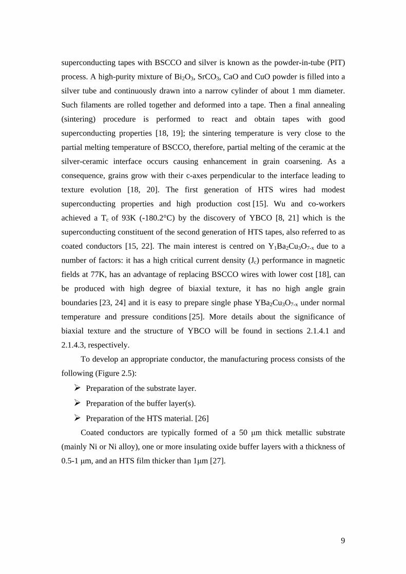
9
superconducting tapes with BSCCO and silver is known as the powder-in-tube (PIT)
process. A high-purity mixture of Bi2O3, SrCO3, CaO and CuO powder is filled into a
silver tube and continuously drawn into a narrow cylinder of about 1 mm diameter.
Such filaments are rolled together and deformed into a tape. Then a final annealing
(sintering) procedure is performed to react and obtain tapes with good
superconducting properties [18, 19]; the sintering temperature is very close to the
partial melting temperature of BSCCO, therefore, partial melting of the ceramic at the
silver-ceramic interface occurs causing enhancement in grain coarsening. As a
consequence, grains grow with their c-axes perpendicular to the interface leading to
texture evolution [18, 20]. The first generation of HTS wires had modest
superconducting properties and high production cost [15]. Wu and co-workers
achieved a Tc of 93K (-180.2°C) by the discovery of YBCO [8, 21] which is the
superconducting constituent of the second generation of HTS tapes, also referred to as
coated conductors [15, 22]. The main interest is centred on Y1Ba2Cu3O7-x due to a
number of factors: it has a high critical current density (Jc) performance in magnetic
fields at 77K, has an advantage of replacing BSCCO wires with lower cost [18], can
be produced with high degree of biaxial texture, it has no high angle grain
boundaries [23, 24] and it is easy to prepare single phase YBa2Cu3O7-x under normal
temperature and pressure conditions [25]. More details about the significance of
biaxial texture and the structure of YBCO will be found in sections 2.1.4.1 and
2.1.4.3, respectively.
To develop an appropriate conductor, the manufacturing process consists of the
following (Figure 2.5):
Preparation of the substrate layer. Preparation of the buffer layer(s). Preparation of the HTS material. [26] Coated conductors are typically formed of a 50 μm thick metallic substrate
(mainly Ni or Ni alloy), one or more insulating oxide buffer layers with a thickness of
0.5-1 μm, and an HTS film thicker than 1μm [27].

10
Figure 2.5: Superconductor architecture [28].
2.1.4.1 The substrate layer
For the development of a reliable deposition technology for high-quality HTS
thin films, the choice of substrate material is of primary importance. The basic
requirements for the substrate can be summarised as follows [29].
Crystallographic lattice match between the HTS film and substrate.
Similar thermal expansion coefficients of HTS and substrate.
No chemical interaction at the interface between HTS and substrate, and
Suitably polished surface, stable and reasonably robust.
Generally two classes of substrates can be distinguished: a) compatible
substrates onto which HTS can be deposited without a buffer layer such as LaAlO3,
SrTiO3 and MgO for YBCO deposition; however, buffer layers may be added for
some compatible substrates to reduce the probability of a-axis growth as is the case of
depositing a CeO2 buffer on LaAlO3 substrates, and b) non-compatible substrates
which have to be covered with an epitaxial buffer layer prior to the deposition of the
HTS film owing to a large lattice mismatch and/or chemical interaction between
substrate and HTS material or owing to missing in-plane orientation as is the case to
get biaxially oriented YBCO on polycrystalline substrates. Table 2.1 lists some
important properties of different materials, which can be used as substrates as well as
buffers or interlayers [29].
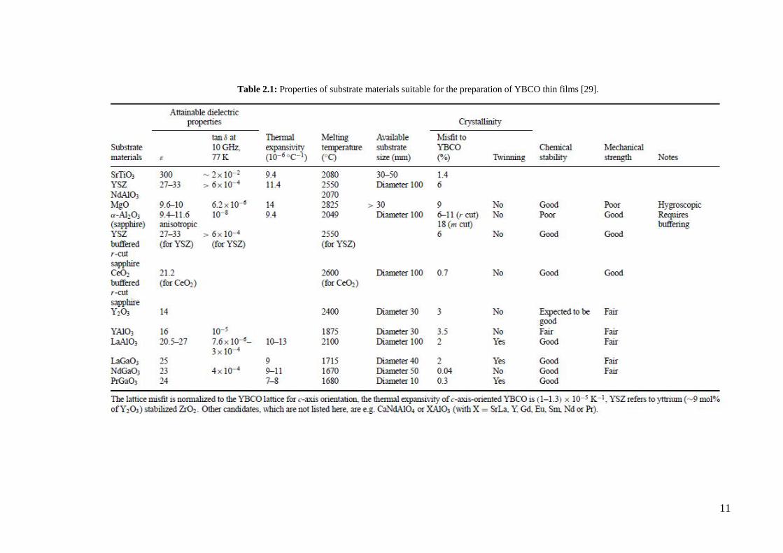
11
Table 2.1: Properties of substrate materials suitable for the preparation of YBCO thin films [29].

12
The fabrication of high temperature superconductors into useful forms with
acceptable superconducting properties has been hindered by many intrinsic material
problems, such as superconducting weak links and poor mechanical properties [15]. It
is known that high angle grain boundaries reduce the potential critical current density
(Jc) value (Figure 2.6) of the superconductor [30, 31], by impeding long range current
flow [6]. Such problems have led to the development of the second generation HTS
tapes which have the potential to carry 100-1000 times the current without resistance
losses of comparable copper wire. HTS power engineering equipment has the
potential to be half the size of conventional alternatives with the same or higher power
rating and less than one half the energy losses [15]. Three methods have been
invented to produce flexible metallic substrates, which were also crystallographically
biaxially textured and resembled a long, mosaic pseudo-single crystal, upon which
epitaxial growth of the superconducting layer was possible to realize a single-crystal-
like HTS tape [15]. These methods are, rolling assisted biaxially textured substrates
(RABiTS) [16, 24, 32-34], Ion beam assisted deposition (IBAD) [33, 35-38] and
inclined substrate deposition (ISD) [39-42].
The RABiTS process involves a thermomechanical [43, 44] biaxial texturing of
a metal or alloy [16]; hot rolling [26] or cold rolling [32, 45] followed by annealing
[26, 32], and then epitaxial deposition of the buffer layers and the superconductor
[16]. The buffer layers are required to prevent Ni diffusion into YBCO which
degrades the superconducting properties. The whole process is demonstrated in Figure
2.7.
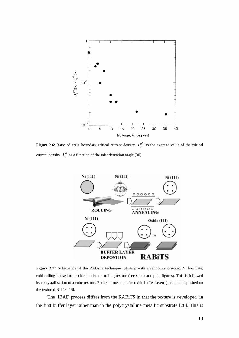
13
Figure 2.6: Ratio of grain boundary critical current density gbCJ to the average value of the critical
current density GCJ as a function of the misorientation angle [30].
Figure 2.7: Schematics of the RABiTS technique. Starting with a randomly oriented Ni bar/plate,
cold-rolling is used to produce a distinct rolling texture (see schematic pole figures). This is followed
by recrystallisation to a cube texture. Epitaxial metal and/or oxide buffer layer(s) are then deposited on
the textured Ni [43, 46].
The IBAD process differs from the RABiTS in that the texture is developed in
the first buffer layer rather than in the polycrystalline metallic substrate [26]. This is

14
accomplished by using an ion beam [47, 48] impinging on the buffer layer (Figure
2.8) which is being laid down simultaneously [15] by vapour phase deposition [26].
Figure 2.8: Textured substrate preparation by IBAD [26].
The biaxial alignment in the ISD method is obtained by inclining the substrate
(Figure 2.9) under specific conditions of pulsed laser deposition (PLD), using
Excimer laser [49], without ion beam assistance [49, 50]. The ISD was first developed
in 1996 to deposit YSZ (yttria stabilised zirconia) on Ni based substrates by PLD [49],
and in 2002, biaxially textured (MgO) on polycrystalline substrates has been grown
successfully by ISD [51] using electron beam evaporation [52, 53].
Figure 2.9: Schematic diagram of inclined substrate deposition (ISD) [49].
2.1.4.2 The buffer layer
The role of the buffer layers, which are commonly ceramic oxides, is mainly to
extend the texture of the substrate into the superconducting film by gradually
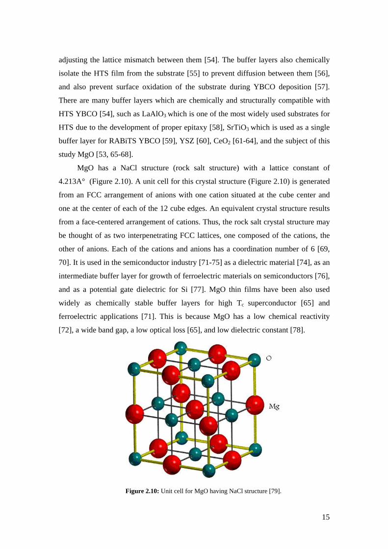
15
adjusting the lattice mismatch between them [54]. The buffer layers also chemically
isolate the HTS film from the substrate [55] to prevent diffusion between them [56],
and also prevent surface oxidation of the substrate during YBCO deposition [57].
There are many buffer layers which are chemically and structurally compatible with
HTS YBCO [54], such as LaAlO3 which is one of the most widely used substrates for
HTS due to the development of proper epitaxy [58], SrTiO3 which is used as a single
buffer layer for RABiTS YBCO [59], YSZ [60], CeO2 [61-64], and the subject of this
study MgO [53, 65-68].
MgO has a NaCl structure (rock salt structure) with a lattice constant of
4.213A° (Figure 2.10). A unit cell for this crystal structure (Figure 2.10) is generated
from an FCC arrangement of anions with one cation situated at the cube center and
one at the center of each of the 12 cube edges. An equivalent crystal structure results
from a face-centered arrangement of cations. Thus, the rock salt crystal structure may
be thought of as two interpenetrating FCC lattices, one composed of the cations, the
other of anions. Each of the cations and anions has a coordination number of 6 [69,
70]. It is used in the semiconductor industry [71-75] as a dielectric material [74], as an
intermediate buffer layer for growth of ferroelectric materials on semiconductors [76],
and as a potential gate dielectric for Si [77]. MgO thin films have been also used
widely as chemically stable buffer layers for high Tc superconductor [65] and
ferroelectric applications [71]. This is because MgO has a low chemical reactivity
[72], a wide band gap, a low optical loss [65], and low dielectric constant [78].
Figure 2.10: Unit cell for MgO having NaCl structure [79].

16
MgO thin films have been prepared by many techniques, either physical [16,
26], such as pulsed laser deposition [65, 80, 81], electron beam evaporation [75, 82],
or chemical [26, 83, 84], such as metal organic chemical vapour deposition [56, 85]
and spray pyrolysis, on Si (100), Si (111), NaCl (100) single crystals, polycrystalline
Al2O3 substrates and glass substrates [56, 65, 67, 72, 78, 86]. More details on the
deposition of MgO by spray pyrolysis will be found in section 2.5.
2.1.4.3 The superconducting layer
YBCO is the most obvious candidate material for conductor applications
because of its high irreversibility field [87]. Biaxially textured YBCO thin films have
been successfully deposited by many techniques such as sputtering [88] and PLD [49,
89]. Those techniques need high vacuum [90]. The non-vacuum methods include
sol-gel [91], metal organic deposition [92], and spray pyrolysis [23, 24, 87, 93, 94].
The YBCO superconductor has a layered perovskite-like and highly anisotropic
structure with a thermal expansion coefficient of 13x10-6°C-1 [95]. YBa2Cu3O7-x
(YBCO-123) is the extensively studied high-temperature superconductor (HTS) for
which Tc exceeds the boiling point of liquid nitrogen (77K at 1atm). It is oxygen
deficient with ordered vacancies, consisting of three unit cells, with four different
layers stacked sequentially as BaO-CuO-BaO-CuO2-Y-CuO2-BaO-CuO-BaO (Figure
2.11). The presence of one or more CuO2 planes in the unit cell is a common feature
of all cuprate superconductors. The Y1Ba2Cu3O7-x has both orthorhombic (x<0.5), the
superconducting phase, and tetragonal (x≥0.5) structures. The lattice parameters for
YBa2Cu3O7 are a= 3.8185Å, b=3.8856Å and c=11.68047Å. A slight difference
between a and b lattice constants in the orthorhombic superconducting phase is caused
by oxygen vacancy ordering in the CuO layer (chains) sandwiched between BaO
layers. The relation between oxygen deficiency (x) and the superconducting transition
temperature is shown in Figure 2.12. Besides the high transition temperature of the
HTSCs (Tc=93K), they also have a pronounced anisotropy. Such anisotropy originates
from the fact that superconductivity occurs mainly in the CuO2 planes [13, 21, 96].

17
Figure 2.11: The unit cell of YBCO-123 [97].
Figure 2.12: Superconducting transition temperature (Tc) as a function of oxygen content for
YBa2Cu3O7-x [98].
Oxide superconductors like YBCO are brittle ceramic materials and therefore
are not amenable to common forming operations. To overcome this problem, YBCO
has been deposited as a thin film on flexible metallic substrates [32]. The growth of
YBCO films on metallic substrates, such as stainless steel or Ni-based superalloys, is
desirable for wires, cables, electromagnetic shields etc. [99]; however, YBCO
18
deposited directly on such substrates exhibits poor superconducting properties [100]
because of interdiffusion problems [99]. For this reason, buffer layers are required.
Some of the HTS applications include: high-power transmission cables,
high-field magnets, magnetic shields and large scale microwave devices [40], HTS
cables assembled by YBCO tapes are also used for AC transmission cables [101], and
many other applications.
2.2 Thin film technology
Thin film deposition is made onto the substrate to obtain properties which are
unattainable or not easily attainable in the substrate alone; for example, Cr coatings
used on plastic parts for automobiles impart hardness, metallic luster, and protection
against ultraviolet light. This functionality is also achieved in the same part made
from bulk metal but on the expense of cost and weight. Another example is titanium
nitride (TiN) coatings on cutting tools which offer hardness, low friction, and
chemical barrier to alloying of the tool with the workpiece. Such properties are
unattainable in a bulk material; since the bulk material must also offer high strength
and toughness in the cutting tool application. Table 2.2 lists some of the required
properties for some of the applications at hand. Usually, multiple properties are
obtainable simultaneously from the same film and additional functionality in thin
films can be obtained by depositing multiple layers of different materials. The films
can be either thin or thick. Thin film involves individual molecule-deposition, while
the thick ones involve particle deposition as in painting and plasma spraying. It is to
be mentioned that the thick film technique does not offer the control or the material
quality of the thin film techniques. Also the films deposited by thin film techniques
can be thicker than those obtained by a thick film technique, such as graphite plates
several millimetres thick deposited by thermal decomposition (pyrolysis) of
hydrocarbon vapours [102].

19
Table 2.2: Thin film applications [102].
Thin film property
category Typical applications
Optical Decoration, Memory discs(CDs)
Electrical Insulation, Conduction, Semiconductor devices
Magnetic Memory discs
Chemical
Barrier to diffusion or alloying, Protection
against oxidation or corrosion
Mechanical Wear resistance coating, Hardness, Adhesion
Thermal Barrier layer, Heat sinks
All thin film processes contain main sequential steps. A source of film material
is provided, the material is transported to the substrate, deposition takes place, and
sometimes the film is subsequently annealed. The source of the film-forming material
may be a solid, liquid, vapour or gas. Solid materials need to be vaporised to transport
them to the substrate. This can be achieved by heat or by energetic beam of electrons,
photons (laser ablation), or positive ions (sputtering). These methods are categorised
as physical vapour deposition (PVD). Thin film processes involving the use of gases,
evaporating liquids, or chemically gasified solids as the source material, are
categorised as chemical vapour deposition (CVD) where the chemical composition of
the product is different from the starting material. In both PVD and CVD,
contamination and supply rate are the major source-material issues. Contamination is
also an issue in the transport and deposition steps. Supply rate is important because
film properties vary with deposition rate and with the ratio of elements supplied to
compound films. The major issue in transporting the film-forming material to the
substrate is the uniformity of arrival rate over the substrate area. The factors affecting
this uniformity are very different, depending on whether the transport medium is a
high vacuum, as in high vacuum PVD, or a fluid (i.e. gaseous medium), as in
fluid-CVD. In vacuum, the molecules travel from the source to the substrate in
straight lines, while in fluid, there are many collisions among molecules during the
transport. According to that, the uniformity of arrival rate at the substrate in high
vacuum medium is determined by geometry. In a fluid medium, it is determined by

20
gas flow patterns and by diffusion of the source molecules through the other gases
present. The advantage of using a high-vacuum transport medium is easy access to the
deposition surface, and it allows energy input from an ion beam and allows the use of
analytical techniques involving electron beams, such as electron diffraction and Auger
spectroscopy. The fluid medium has the advantage that it uses atmospheric pressure or
an easily-achieved moderate vacuum level.
The deposition behaviour of the thin film onto the substrate is determined by the
source, transport factors and by conditions at the deposition surface. The surface
factors include: substrate surface conditions, reactivity of the arriving material and
energy input. Substrate surface condition includes roughness, level of contamination,
degree of chemical bonding with the arriving material and crystallographic parameters
in the case of epitaxy. The reactivity is the probability of arriving molecules to react
with the surface and becoming incorporated into the film. This probability is termed
the sticking coefficient (αs) which varies from unity to less than 10-3. It is usually
lower for CVD than for PVD processes, the low values of αs aids in coating
convoluted shapes and in deposition on selected areas.
The energy input into the surface can come in many forms. It has a large effect
on the reactivity of the arriving material, the composition and structure of the film.
The basic source of energy input is the substrate temperature. Other sources include
photons, and chemical energy carried by reactive source molecules and by molecules
that have been dissociated in the course of vaporisation. So, the substrate condition,
reactivity and energy input, all work together with the arriving fluxes to determine the
structure and composition of the deposited film which in turn determine the film
properties [102].
2.2.1 Epitaxy
Woodcock [103] made a survey for the term epitaxy. He found that many
definitions were given to epitaxy. The Longman Dictionary of Physics gives it as: ‘‘A
method of growing a thin layer of material upon a single crystal substrate so that the
lattice structure is identical to that of the substrate’’. The Oxford Dictionary of
Physics defined epitaxy as: ‘‘Growth of a layer of one substance on a single crystal of
another, such that the crystal structure in the layer is the same as that in the
substrate’’. This implies that the film deposited on a BCC substrate, for example,

21
would only be called as epitaxial if it also had a BCC structure as well. On the
contrary, the term epitaxial is also used to describe YBCO films, which have an
orthorhombic crystal structure, on polycrystalline or biaxially textured metallic
substrates buffered with cubic oxides [44, 89, 100, 104, 105].
Woodcock [103] found that the dictionary definitions and common usages of
the term epitaxial differ considerably and some clarification of the parameters used to
assign films as epitaxial is needed. He defined, epitaxy (or epitaxial growth) as:
‘‘Growth of a film exhibiting a characteristic orientation relationship with a substrate,
dictated by the minimisation of structural disorder at the film/substrate interface’’.
Thus, epitaxial growth of a film on a textured substrate will result in a textured film.
Epitaxy also means that the crystallographic order of the film is being
significantly influenced by that of the substrate as a result of some degree of matching
between the two along the interface [102]. It is also defined as the condition in which
lattice planes on one side of a boundary are parallel to those on the other [106].
Another definition is the growth process of a solid film on a crystalline substrate in
which the atoms of the growing film mimic the arrangement of the atoms of the
substrate.
The growth processes of thin epitaxial films are essentially the same as that of
bulk crystals, except for the influence of the substrate at the initial stages. This
influence comes from the lattice misfit and thermal stresses, from the defects
appearing at the substrate-film interface and from the chemical interactions between
the film and the substrate. Frankenheim [107] was the first to successfully obtain
epitaxy of alkali-halide deposits from a solution onto a cleaved mica surface.
Five possible modes of crystal growth can be distinguished in epitaxy (Figure
2.13): Volmer-Weber, Frank-van der Merve, Stranski Krastanov, columnar and step
flow mode. The mode by which the epitaxial film grows depends upon the lattice
misfit between substrate and film, the growth temperature and adhesion energy.
During island or Volmer Weber growth, small clusters are nucleated directly on
the substrate surface. The clusters then grow into islands, which in turn coalesce to
form a continuous film. This type of growth occurs when the film atoms, or
molecules, are more strongly bound to each other than to the substrate as in the case
for metal films growing on insulators. Layer-by-layer, or Frank-van der Merve,
growth occurs when the binding between film atoms is less than that between the film
atoms and the substrate. Examples of layer-by-layer growth are the metal on metal

22
system as well as the semiconductor on semiconductor system. The third growth
mode often referred as Stranski-Krastanov, or layer plus island growth mode, is an
intermediate case. In this case after forming one or more monolayers, further layer
growth becomes unfavourable and islands are formed on top of this intermediate
layer. The transition from layer-by-layer to island growth is not completely
understood. The columnar growth mode shows some similarities with the Stranski
Krastanov and Volmer Weber modes, but it is fundamentally different. In the case of
the Stranski Krastanov and Volmer Weber growth, when the film thickens, the
condensed phase islands characteristic to these modes tend to merge and to cover the
whole substrate surface. In contrast the columns are not merging when the film is
grown according to the columnar growth mechanism. As a result, columns usually
remain separated throughout the growth process of the film, and the film grown in this
way is easily fractured. The columnar growth mode occurs where low atomic mobility
over the substrate surface leads to the formation of highly defective atomic columns
of the deposited material on this surface.
Beside these described growth modes, in many cases of high quality epitaxy, the
so-called step-flow growth mode is observed. When the substrate wafer is cut slightly
misoriented from a low-index plane in a specific direction, its surface breaks up into
monoatomic steps with precisely oriented low-index terraces and edges. Nucleation
may occur on the terraces when the substrate temperature is sufficiently low or the
flux of the constituent elements of the growing film is high enough to prohibit fast
surface migration of the species adsorbed on the terraces. In this case the film may
grow on the terraces in the Frank-van der Merve or Stranski Krastanov mode.
However, when the substrate temperature is high enough or the flux is sufficiently
low, then the adatoms can be so mobile that they become incorporated directly into
the step edges. In this case growth of the epitaxial film occurs by the advancement of
steps along the terraces [107-109].

23
Figure 2.13: Schematic representation of the five crystal growth modes frequently occurring on flat
surfaces of substrate crystals: (a) layer-by-layer or Frank-van der Merve, (b) step flow, (c) layer plus
island or Stranski-Krastanov, (d) island or Volmer-Weber, (e) columnar growth mode. θ represents the
coverage in monolayers (ML) [108].
2.3 Spray pyrolysis for film formation
Aerosol (used to describe solid or liquid particles suspended in a gas) routes are
used mainly for particle formation but they can also be used for the fabrication or
modification of films. However, relative to aerosol routes for particle formation, the
routes used for film fabrication are less well understood.
Many criteria must be considered when fabricating films. Most applications
require high purity films to optimise electrical, magnetic and optical properties. Metal
films, for example must possess low resistivities which cannot be attained when
carbon and oxygen impurities are present. The microstructure is another criterion that
must be considered, for instance, high temperature superconducting ceramics must be
single crystal films to maximize their current-carrying capacity. The film morphology
has a profound effect on film properties. Even if the film may be of high purity;
poorly connected grains can be formed, leading to high resistivities for metals. In the
case of superconductors, it should consist of highly connected grains to reduce the
resistance. Controlled stoichiometry, precursor cost, and many more factors must also
be considered [110].
Spray pyrolysis is defined as the aerosol process that atomises a solution and
heats the droplets to produce solid products [111]. Spray pyrolysis (droplet
deposition) involves the deposition of evaporating droplets containing reactants onto
surfaces, followed by further solvent evaporation and chemical reaction on the surface

24
[110]. Since the pioneering work by Chamberlin and Skarman in 1966 [112] on
cadmium sulphide films for solar cells, many studies have been performed on spray
pyrolysis for the preparation of thin films of noble metals, metal oxides, spinel oxides
and superconducting compounds [113]; because it is a simple, inexpensive [114], non-
vacuum technique [115], and it has a high deposition rate [87]. Spray pyrolysis is used
for the preparation of thin and thick films, and it is employed for the deposition of
dense and porous films and for powder production [84]. Typical spray pyrolysis
equipment consists of [84] (Figure 2.14):
Atomiser
Precursor solution
Substrate heater
Temperature controller
Figure 2.14: Schematic diagram of the spray pyrolysis equipment [84].
Many atomisers (also called nebulizers) are used to convert bulk liquids into
droplets during spray pyrolysis. Some of them will be mentioned briefly here and the
focus will be on the ultrasonic nebulizer; the one used in this work.
In the pneumatic nebuliser, the solution is exposed to air blast [116] where the
energy of the air or a carrier gas is used to break up sheets or jets of a liquid.
Pneumatic atomisers are the most complex of the atomisers because the liquid and gas
phases interact in a complex manner [110]. In the electrostatic nebuliser, DC voltage
is applied between an electrically conductive substrate and a metal capillary nozzle,
which is connected to a precursor solution, to generate the spray which moves toward
the heated substrate by the electrostatic force [117]. The electrostatic atomisation
depends on the electrical conductivity of the liquid and produces droplet sizes in the
range of sub-microns to millimetres and is used mainly on the laboratory scale

25
because it does not allow simultaneous high liquid flow rates and submicron droplets.
However they have the advantage that the charged droplets can be deposited onto
surfaces even in the presence of thermophoretic forces, which drive the particles away
from hot surfaces [110].
The ultrasonic nebuliser, which is used in this work, is used to obtain uniformly
distributed micrometer and submicron-size droplets [118] by using ultrasonic
frequencies to produce short wavelengths that are necessary for fine atomisation [84].
The atomised droplets are then transported to the heated substrate through a pipe by a
neutral gas (e.g. Argon) [113]. Ultrasonic atomisers use an ultrasonic transducer that
vibrates at ultrasonic frequencies (usually, 50 KHz – 2.4 MHz) to produce the short
wavelengths required for liquid atomisation. The ultrasonic atomisers are used
extensively in aerosol methods for generating films and powders at laboratory and
industrial scale. The reason behind that is the low spray velocity of the ultrasonic
atomisers, the small amount of carrier gas required to operate them and the small
droplet size produced. This makes it easy to carry small droplets at a high
concentration towards a surface without using a high gas flow [110].
There are three classes of ultrasonic atomisers. In the first class, the liquid
passes through a tube that is driven ultrasonically. In the second class, the liquid
comes into contact with an ultrasonic horn. In the third class, an ultrasonic transducer
is submerged in the liquid. The principle of operation in all of the classes is the same.
When a liquid comes into contact with an ultrasonically driven surface, a wave pattern
appears on the surface of the liquid. When the amplitude of the vibration is sufficient,
the wave height is sufficient for the wave crest in the film to become unstable. This
instability drives the formation of droplets, which are ejected from the surface. A
carrier gas can then be used to sweep the droplets away from the surface.
The submerged ultrasonic transducers, the one adapted in this work, can provide
1 to 5µm droplets for frequencies of 1.5 to 2.4MHz with low gas flow rates that
correspond to high droplet concentrations. The sizes produced by the submerged
ultrasonic transducers are much smaller than those produced with the other ultrasonic
types, which produce droplets with mass median diameters of 20 µm and larger. The
droplet size depends on the surface tension and density of the fluid, and frequency of
the ultrasonic source according to the following equation [110]:
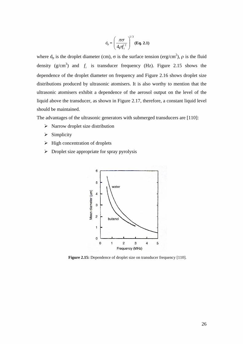
26
dp =
3/1
24 ⎟⎟⎠
⎞⎜⎜⎝
⎛
tfρπσ
(Eq. 2.1)
where dp is the droplet diameter (cm), σ is the surface tension (erg/cm2), ρ is the fluid
density (g/cm3) and tf is transducer frequency (Hz). Figure 2.15 shows the
dependence of the droplet diameter on frequency and Figure 2.16 shows droplet size
distributions produced by ultrasonic atomisers. It is also worthy to mention that the
ultrasonic atomisers exhibit a dependence of the aerosol output on the level of the
liquid above the transducer, as shown in Figure 2.17, therefore, a constant liquid level
should be maintained.
The advantages of the ultrasonic generators with submerged transducers are [110]:
Narrow droplet size distribution
Simplicity
High concentration of droplets
Droplet size appropriate for spray pyrolysis
Figure 2.15: Dependence of droplet size on transducer frequency [110].

27
Figure 2.16: Number (dotted)) and volume (solid) distribution of water droplets [119, 120].
Figure 2.17: Dependence of aerosol flow as a function of liquid level above transducer [119].
Undesirable situations may occur during droplet deposition. As the droplet
approaches the heated substrate, solvent will evaporate and if the evaporation is
enough, only solid particles of the precursor(s) will deposit to form the film. This
situation is unfavourable as it results in porous films. Particles that became
sufficiently small in the gas phase may not deposit if their inertia is low enough to
avoid impaction and the particles follow the gas flow away from the substrate (Figure
2.18). It is also important to mention that in spray pyrolysis, the rate of deposition
decreases with increasing temperature as a result of the different mechanism of
deposition; the thermophoretic velocity driving the droplets away from the surface is
higher at higher substrate temperatures and the droplet evaporation is more rapid,
leading to smaller droplets that are better able to flow with the gas [110].

28
Figure 2.18: Droplets of different sizes can behave differently during deposition [110].
To synthesize thin films of the required material, it is important to know the
details of the deposition conditions as well the details of the chemical thermal
decomposition processes [83]. There is no clear explanation of the processes
occurring during deposition. However, four modes for the deposition and
decomposition processes may be distinguished (Figure 2.19) [83, 120].
Figure 2.19: Possible working modes that may occur during deposition [83].

29
“In the first mode (1), the aerosol droplets splash on the surface of the heated
substrate, the solvent vaporizes and the decomposition of already dry precipitates
directly on the substrate follows. In the second mode (2), rather similar to the first
one, only dry precipitates come to the surface, where thermal decomposition takes
place. We may designate the decomposition processes of these two working modes as
‘‘true pyrolysis’’, because the thermal decomposition takes place on the surface of a
heated substrate only. As a true CVD ‘chemical vapour deposition’ mode we consider
the third mode (3), when thermal decomposition of dry precipitates starts on their way
to the substrate. In this case mainly vapour arrives at the substrate surface. In the
fourth mode (4), the full thermal decomposition takes place outside the substrate and
only finely divided solid product arrives at the substrate surface. Also it is to be noted
that the actual working mode depends not only on the substrate temperature, but also
on the temperature of the working surrounding” [83].
Thin films can also be deposited by AACVD which involves chemical vapour
deposition onto a heated substrate with aerosol delivery of precursors, whether in
solution or solid-particle form. The major distinction between spray pyrolysis and
AACVD is that in AACVD the precursor also evaporates and then adsorbs and reacts
on the surface to form a film. The droplets are usually formed by spray routes in
which volatile precursors are dissolved in liquids that are atomised. Alternatively,
solid particles of the reactant can be entrained in a gas to form an aerosol that
evaporates at least partially before reaching the substrate. This process is then
followed by CVD [110]. The main distinction between AACVD and CVD is the
method by which the precursors are delivered to the substrate. The theory of CVD is
well developed, however, no full models have been developed to describe AACVD.
One of the largest applications for AACVD technique is the deposition of
multicomponent films. Figure 2.20 shows the different modes of behaviour of
AACVD, where three cases can be distinguished for precursors A, B and C. The
simplest case is evaporation of the precursor followed by CVD. Another case is
incomplete evaporation of the precursor particles. In the last case, the precursors
evaporate either partially or completely and then react in the gas phase to give
products (D, E and F) that deposit on the surface or perhaps also form particles in the
gas phase.

30
Figure 2.20: Possible behaviour modes of AACVD [110].
2.4 Aerosol techniques
Aerosol techniques are the science involved in the synthesis and processing of
powders and films. Historically, the term aerosol is used to describe solid or liquid
particles suspended in a gas and it can be formed as a result of wide variety of
processes. Those processes can be classified into physical and chemical ones. An
example of the physical processes, where the chemical composition of material is the
same before and after processing but the form of the material is changed from bulk to
particles, is the direct ejection of particles from surfaces into a gas. An example of the
chemical processes, where the composition of the precursor is different from that of
the final product, is the chemical vapor deposition of volatile species being evaporated
from an aerosol and spray pyrolysis, the subject of this work.
Materials produced by aerosol processes may be a single crystal, which is an
extreme case, may exhibit a preferred orientation (in the case of films), or, at the
opposite end, may be amorphous. The crystallinity of the film or powder can be
controlled through the processing conditions, mainly temperature and time history of
the process [110, 111].
It should be mentioned that the equations mentioned in this section are used for
giving the reader an idea about the different processes occurring during spray
pyrolysis. However, non of them are applicable to the spray pyrolysis system used in
this work due to different reasons; the increase in the droplet life time due to the
presence of solute in droplets and the increase in the evaporation rate due to heating of
31
the gas above the substrate were neglected. These effects would affect the deposition
process as will be seen in the following sections.
2.4.1 Technologies for generating powders and films
The technologies for generating powders and films can be divided, according to
how the final product is produced, into gas-to-particle conversion, intraparticle
reaction processes and bulk-to-particle direct ejection or entrainment processes.
An example of bulk-to-particle direct ejection is the laser ablation and
sputtering in certain modes of operation [110]. PLD is used to deposit thin films of
buffer materials or YBCO and in this work it is used to deposit YBCO and CeO2. The
laser beam is focused down by a lens and hits a target of the desired material at ~45°
angle. The incident laser beam creates a plume of the material perpendicular to the
target surface. The heated substrate is placed in the plume path. PLD is very suitable
for the controlled deposition of complex multi-elemental thin films with a desired
stoichiometry. The deposited material can range from nano-particles to thin films
(amorphous, polycrystalline, single crystal) [121, 122].
2.4.1.1 Gas to particle conversion
In this approach condensable gaseous (atomic or molecular) species are used to
form supersaturated vapor (the atoms or molecules of a given species present at partial
pressure higher than the vapor pressure of that species) by either a chemical reaction
that creates new species or as a result of physical processes such as cooling that
reduce the vapor pressure of condensable species. Due to the supersaturation, new
particles form by homogenous nucleation. The particle growth can then follow by
physical condensation of vapor onto particles, by chemical reaction on the particle
surface, or by diffusion of the reactant into a particle, followed by reaction within the
bulk of the particle. At high particle concentration and normally at high temperatures,
coalescence can occur to form a single spherical particle. Finally agglomeration
results from collisions between particles to form a collection of particles [110].
Gas-to-particle conversion processes can be coupled with particle deposition
from the gas phase to provide methods for fabricating films. Such deposition can be
accomplished by mechanisms that include [110]:
Thermophoresis, where particle motion is induced by a temperature gradient in a
gas by which the particles move from high to low temperature regions. It is

32
responsible for particle deposits at cold spots on reactor walls and exhaust tubes. It
reduces the deposition rates during aerosol assisted CVD, droplet deposition, and
solid particle deposition onto heated surfaces. In thin films, thermophoresis
provides, when the substrate temperature is greater then that of the gas, the driving
force to keep particles that are suspended in a cool gas stream from striking a hot
surface, keeping them from penetrating into hotter regions of the gas where their
evaporation rates would be increased [123].
Electrophoresis: it is the charging of particles by an electric field to increase the
transport rate of particles to regions near to the hot surface, where the precursors
can evaporate.
Diffusion of particles is a mechanism by which collisions occur between particles
larger than the gas mean free path (is to be explained in more details in section
2.4.1.1.1), and it is a mechanism of particle deposition onto surfaces when the
particle size is sufficiently small and diffusion distance sufficiently short, as in
CVD processes in which particles can be formed just above the surface of a
material.
Deposition can also be achieved by impaction. Particles follow the gas stream
lines, neglecting other forces such as electrophoretic and thermophoretic, until the
fluid stream changes direction, as in the case of a bend or obstruction in a pipe or
aerosol spraying of a substrate using a jet of gas. Large particles cannot follow this
change; inertia forces them to move in the original direction and impact. On the
other hand, small particles follow the gas flow (Figure 2.21). The impaction
technique is used to form films by the depositing droplets onto surfaces during
spray pyrolysis [110].
Figure 2.21: Schematic of the impaction mechanism [123].

33
The above basic deposition phenomena are also common to a variety of film
generation routes including solid-particle deposition, spray pyrolysis, and aerosol
assisted chemical vapour deposition (AACVD) (Figure 2.22). The mechanisms
underlying these phenomena are shown in Figure 2.23.
Figure 2.22: Role of particle deposition in various processes for film fabrication [110].
Figure 2.23: Particle transport phenomena [110].
2.4.1.1.1 Mean free path of the gas
To describe aerosol processes, several variables, such as precursor and product
characteristics, must be considered. More specifically, particle size distribution and
composition (which determine vapor pressure, for example) are the most important
parameters. Control of the aerosol processes for the production of materials also
34
requires understanding the interaction between the aerosol components i.e. gas and
particles. The nature of this interaction is largely determined by the particle size and
mean free path of the gas [124].
The mean free path of a gas (λ) is one of the most important characteristics
associated with an aerosol. It is the average distance that a molecule or atom of the
gas travels before colliding with another atom, another molecule, or the walls. A
major difference between gases and liquids is that the λ for gas molecules is larger; as
a consequence gas molecules travel relatively long distances before colliding with
each other. This is because the molecules and atoms in liquids are separated by
distances roughly equal to molecular or atomic diameters, while the molecules and
atoms in gases are separated by distances much larger than that.
The average distance (cm) traveled by the molecules between collisions is given
by:
λ = __
00.2
Cρ
μ (Eq. 2.2)
where µ (g/cm sec) and ρ (g/cm3) are the gas viscosity and density, respectively. C
(cm/sec) is the average of the velocities of all the gas molecules.
When the particle diameter is much larger than the mean free path (dp>>λ), the
particle sees the gas as a continuous medium. However, when (dp<<λ), in this case
each particle behaves as if it were in a rarefied medium in which the particles do not
influence the velocity distribution of surrounding molecules and atoms (Figure 2.24).
The Knudsen number (Kn = 2λ/dP) is used to simplify analysis involving particle size
and gas mean free path. It is defined as the ratio of the mean free path of the gas to the
particle radius. When Kn << 1 the particles are said to be in the continuum regime and
when Kn >> 1, the particles are in the free molecular regime. For the case where
0.1λ < dP < 10λ, the particles are in the transition-slip regime, since the particles slip
effectively between the gas molecules.

35
Figure 2.24: Relation between particle sizes and mean free path for a) continuum regime and b) free
molecular regime [110].
2.4.1.2 Intraparticle reaction processes
Some of these processes are called evaporative decomposition, spray roasting
and spray pyrolysis, the subject of this work. Intraparticle processes are important
during powder formation by spray pyrolysis, vacuum atomization of molten metals,
droplet-phase reactions to form liquid or solid products. It is also important for film
formation by AACVD when the volatile precursor in each droplet reacts before
evaporating. In Intraparticle reaction processes the particles containing the precursor
are formed mechanically by a droplet or particle generator. The precursor is then
reacted with a gas or pyrolysed in the particle to form the product. This can be done
with the aid of a hot wall, a flame or any energy source that heats the particles [110].
There are several classes of Intraparticle processes, as follows:
Gas-solid reactions: they occur at the interface of particles with a gas, or the
gaseous species can diffuse into a porous solid, where the reaction occurs. Such
reactions are important for the formation of materials, especially for
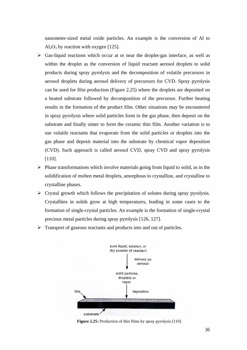
36
nanometer-sized metal oxide particles. An example is the conversion of Al to
Al2O3 by reaction with oxygen [125].
Gas-liquid reactions which occur at or near the droplet-gas interface, as well as
within the droplet as the conversion of liquid reactant aerosol droplets to solid
products during spray pyrolysis and the decomposition of volatile precursors in
aerosol droplets during aerosol delivery of precursors for CVD. Spray pyrolysis
can be used for film production (Figure 2.25) where the droplets are deposited on
a heated substrate followed by decomposition of the precursor. Further heating
results in the formation of the product film. Other situations may be encountered
in spray pyrolysis where solid particles form in the gas phase, then deposit on the
substrate and finally sinter to form the ceramic thin film. Another variation is to
use volatile reactants that evaporate from the solid particles or droplets into the
gas phase and deposit material into the substrate by chemical vapor deposition
(CVD). Such approach is called aerosol CVD, spray CVD and spray pyrolysis
[110].
Phase transformations which involve materials going from liquid to solid, as in the
solidification of molten metal droplets, amorphous to crystalline, and crystalline to
crystalline phases.
Crystal growth which follows the precipitation of solutes during spray pyrolysis.
Crystallites in solids grow at high temperatures, leading in some cases to the
formation of single-crystal particles. An example is the formation of single-crystal
precious metal particles during spray pyrolysis [126, 127].
Transport of gaseous reactants and products into and out of particles.
Figure 2.25: Production of thin films by spray pyrolysis [110].
37
Diffusion is the mechanism by which transport occurs during intraparticle
processes. Diffusive transport, the movement of species due to their random thermal
motion in a concentration gradient, occurs in solids, liquids and gases. Reactants are
transported into the interior of particles and reaction products are removed from the
interior of the particles by diffusion. Diffusion is also the process that enables crystal
growth inside particles after solute precipitation in droplets. Diffusion processes are
often driven by concentration gradients caused by reactions inside particles or droplets
or by transport processes outside the particles. They can also be driven by surface
curvature. In spray pyrolysis, particles are formed by the diffusion of the solvent
through the droplet to the surface, where it then evaporates and diffuses into the gas
phase. At the same time, the solute must diffuse towards the center of the particle.
This results in concentration gradients of the solute in the droplet that are the cause of
precipitation of species at the droplet surface, which can lead to formation of a shell.
The diffusing species must then also diffuse through this shell [128].
2.4.2 Chemistry of aerosol processes
Chemical processes that occur during the aerosol synthesis of materials can be
classified in terms of the final product (i.e. film or powder) or according to the phase
in which they occur (i.e. solid, liquid, or gas). Whichever classification is used, there
is a significant amount of overlap between each classification. In addition to that, it is
difficult to determine whether gas-phase, liquid-phase or solid-state reactions occur
during aerosol synthesis of material. For example, film deposition can occur by
simultaneous particle deposition or CVD.
Film deposition can occur by spray pyrolysis (droplet deposition), solid particle
deposition, and CVD. In spray pyrolysis, a droplet composed of the solvent and the
metal-containing precursor is delivered to a heated substrate, where the solvent
evaporates and the precursor react to form a film of the desired material. In this case,
the solubilities and volatilities of the metal-containing precursors, their reactivities
individually and with each other on the heated substrate are all important; the
reactivity of the metal-containing precursor is crucial to the purity, composition and
value of the product of the process. Also it is desirable that the precursor be
non-volatile to avoid gas-phase processes and retain control over the deposition
process. The volatility of a given species increases with increasing the temperature
and with decreasing the molecular weight. The solvent may also play a role in

38
determining the purity and composition of the produced film. CVD involves the
delivery of vapour-phase precursors using an aerosol delivery process to the surface
where reaction to deposit a film occurs. Gas-phase reaction can lead to the formation
of undesired particles which may be deposited on the surface. In CVD it is important
that the precursors be volatile and capable of reacting on the substrate surface to form
high purity films. When complex materials are to be deposited, the relative vapour
pressures (volatility) and reactivities of the precursors are again important.
The solubility of a solute in a solvent is important in aerosol processes in which
the solute (or metal containing precursor) is first dissolved in a solvent in order to
deliver the solute to the system. Two such processes are spray pyrolysis and AACVD.
Solubility can affect particle morphology through different solubilities of the reagent,
compositional homogeneity during powder formation and different transport rates
during film deposition. Water is often a choice as a solvent for spray pyrolysis
because it exhibits a high dielectric constant, i.e. has high ability to dissolve ionic
species and is used mainly to dissolve metal nitrates. Another solvent property which
should be considered is the donor or coordinating ability of the solvent i.e. its ability
to coordinate to a particular metal (acceptor) center, which depends on the nature of
the solvent and the metal center to which electrons are being donated and is an
important aspect of dissolving a metal-containing compound. The donor/acceptor
ability of solvents has been quantified using donor/acceptor numbers. A higher
numerical value indicates a stronger donor or acceptor; this can be used as a guide to
help dissolve reagents by choosing a better donor solvent over a weaker donor solvent
to improve solubility [129].
Table 2.3 shows an example of donor and acceptor numbers. The donor number
is the negative of the standard reaction enthalpy for the reaction between the donor in
question with the acceptor SbCl5 in 1,2-dichloroethane. The acceptor number is an
arbitrary number derived from the change in nuclear magnetic resonance (NMR)
chemical shift when trimethylphosphine oxide (Me3PO) is used as a reference base
and given a value of 0, while a value of 100 is given to the acceptor SbCl5. The
solubilities of common reagents in water are given in Table 2.4.

39
Table 2.3: Donor and acceptor numbers for various solvents at 298K [110].
Solvent Donor number Acceptor number
Acetic acid - 52.9
Acetone 17.0 12.5
Benzene 0.1 8.2
Carbon tetrachloride - 8.6
Diethyl ether 19.2 3.9
Dimethylsulfoxide 29.8 19.3
Ethanol 19.0 37.1
Pyridine 33.1 14.2
Tetrahydrofuran 20.0 8.0
Water 18 54.8

40
Table 2.4: Solubilities of some metal-containing compounds at 298K. (Superscripts are in °C) [110].
2.4.2.1 Thermal decomposition of precursors
Compounds such as metal nitrates, carbonates and sulfates have been employed
extensively for the formation of metal-oxide-based materials by aerosol processes,
such as spray pyrolysis. Metal nitrates are the most commonly used precursor for
metal oxides because of their lack of carbon, hence avoiding carbon contamination.
Therefore, the discussion in this section will concentrate on the metal nitrates which
are used in this work - the precursor materials and their thermal decomposition

41
behaviour. Metal acetates were also used as a precursor in this work and will be
represented in section 8.2.1.
Although the reaction mechanisms have not been studied in detail during
aerosol-processing experiments, a great deal is known about the thermal
decomposition of metal nitrates in the solid state. In general, metal nitrates decompose
thermally, by heating, to form the corresponding metal oxide, together with NO2, NO
and O2, in various stoichiometries:
M(NO3)2 MO + xNO2 +yNO + zO2 (Eq. 2.3)
MO M+ 21 O2 (Eq. 2.4)
Noble metals such as Ag and Pd, tend to react further and lose O2 at higher
temperatures, forming the corresponding metals.
It is worth mentioning that the solvent has a potential importance in a thermal
decomposition reaction and may play a significant role in the composition and phase
evolution of the system. As an example, nickel nitrate, Ni(NO3)2, thermally
decomposes in a single process to form NO2, O2 and NiO. However, the
corresponding hydrate, Ni(NO3)2.2H2O, decomposes thermally in two steps; first by
forming a mixture of Ni(NO3)2 and Ni(OH)2 and second by dehydration and loss of
NO2 and O2 which results in the formation of NiO [130].
2.4.2.2 Surface processes
During the deposition of thin films on heated surfaces, many surface processes
are involved. The deposition process starts by the transport of molecular species to the
surface where they can physically adsorbed by the formation of a weak interaction
between the surface and the molecules. This can then be followed by chemical
adsorption, in which bonds in the molecular species are broken and new bonds are
formed between fragments of the molecular species and the surface. The species
formed on the surface are usually very reactive and can undergo further chemical
reactions, which results in the formation of reactive species, such as metal atoms and
organic by-products. The metal nuclei generally possess high diffusion coefficients at
the deposition temperature and migrate freely across the substrate surface to positions
of greater thermodynamic stability, which is often another atom or part of a growing
film. This migration ultimately results in additional film growth. The organic
by-products can be rearranged on the surface resulting in their entrainment on the

42
growing film, which is undesirable since it can lead to contamination of the film
through the formation of metal carbides, or the incorporation of carbon into the film,
which may be detrimental to its properties [131]
2.4.3 Particle growth, evaporation and nucleation phenomena in
aerosols
2.4.3.1 Introduction
Growth of particles, evaporation of droplets and formation of new particles are
all exhibited by aerosol processes. Evaporation and condensation of gaseous species
from and onto particles can occur for both droplets and solid particles and it is one of
the ways particles grow and shrink in size after they are formed, often by nucleation.
In droplets, condensation and evaporation occur onto and from a liquid and require a
change in phase from vapour to liquid or vice versa. For solid particles, atomic and
molecular species can physically or chemically adsorb onto the surfaces. On one
hand, the physical adsorption involves the formation of weak attractions such as van
der Waals and is important only for species with partial pressures near their vapour
pressure. On the other hand, the chemical adsorption involves the formation of
chemical bonds with the surfaces and can occur at any temperature and partial
pressure. This is the mechanism by which many solid particles grow.
Condensation and evaporation is an important concept in a wide variety of
aerosol processes for the synthesis and processing of materials. Film formation by the
deposition of droplets onto surfaces (spray pyrolysis) involves directing the droplets at
hot surfaces. The gas temperature rises as the droplets approach the surface, resulting
in evaporation of the liquid and result in a decrease in the size of droplet. In aerosol
assisted chemical vapour deposition (AACVD), volatile precursors, either in solution
or as a pure liquid, are transported by droplets to a region where the solvent and
precursor evaporate to form a vapour of the reactant on the surface to form a film or,
in the gas phase, to form particles.
Spray pyrolysis for the production of powder involves converting a liquid
containing a precursor, in a solution or as a suspension, into aerosol droplets. A heated
gas is used to evaporate the droplets, yielding particles of the reactant. The final
product is then obtained by decomposition of the particles at high temperatures. The
particles can grow and shrink by condensation and sublimation, respectively. Such
43
particles can be used to deliver precursors for chemical vapour deposition (CVD)
processes in the same manner to that for aerosol assisted chemical vapour deposition
(AACVD) with droplets. Solid particles of volatile reactants can be deposited onto
surfaces if they do not evaporate before deposition. Surface reaction is a particle
growth mechanism in which volatile reactants chemically adsorb on particle surfaces
and react to form a product with a low vapour pressure, which then remains on the
particle surface. The transportation and chemical adsorption of co-reactants such as
oxygen are required for such reactions to take place.
The transport of gaseous species onto particle surfaces by evaporation and
condensation also play central roles in the theory of gas-phase nucleation, that is, the
formation of new particles [110, 132].
2.4.3.2 Qualitative particle growth
Before addressing the details of particle formation and growth, a summary of
how the various phenomena are related would be useful. For the example of particle
formation followed by growth, the overall process begins with the formation of new
particles by homogenous nucleation; the one when condensation of vapour takes place
on clusters of similar vapour molecules [132]. In situations when collisions do not
occur, growth often occurs by vapour condensation. After the formation of the
particles, vapour diffusion takes place, with a much shorter time than growth.
The transport of atomic and molecular species to and from particle surfaces is
encountered in many material-processing applications and is the start point to the
theory of condensation, evaporation and surface reaction [133]. The simplest case of
molecular transport to a particle surface is when the particle size is much smaller than
the gas mean free path i.e. in the free molecular regime (dp<<λ), where the molecules
arrive at the particle surface in a ballistic fashion (Figure 2.26). This occurs for
particles smaller than 10nm at standard temperature and pressure. Physically, the
particle is so small that it fits into the spaces between gas molecules and atoms and
behaves like a large molecule.

44
Figure 2.26: Schematic of atoms and / or molecules (A) colliding with a particle in the free molecular
regime [110].
From the kinetic theory of gases, the rate of change of the particle (solid or
liquid) diameter with time at temperature T in the free molecular regime (Kn>>1) is
given by:
dtdd p
= 12/11
11
)2()(2
FTkm
pp
B
ds
πνα −
(Eq. 2.5)
Where:
dp: the particle diameter.
t : the time.
αs: the sticking coefficient.
ν1: is the volume of transported molecule or atom in the particle = m1 / ρ1.
m1 = M / NA , the mass of transported molecule or atom in the particle.
ρ1: is the density of the material in the particle in the solid or liquid state.
M: the molecular weight.
NA: Avogadro’s number.
p1: the partial pressure of the vapour for species 1 far from the particle.
pd: the partial pressure at the particle surface.
kB: Boltzmann’s constant.
T: the temperature.
F1: correction factor.
Particle
: Atom and/ or molecule A

45
In the continuum regime, the transport mechanism by which atoms and
molecules move to and from a particle's surface is diffusion, which occurs when the
particle size is much larger than the gas mean free path, or about 1000 nm at standard
temperature and pressure. The gaseous species being transported undergo numerous
collisions with other gas molecules on its way to or from the particle surface (Figure
2.27). In addition, during condensation, evaporation or sublimation, a concentration
gradient can be established around the particles.
Figure 2.27: Schematic illustrating how atoms and molecules are transported to a particle surface by
diffusion in the continuum regime [110].
The rate of change of particle diameter with time at a temperature T in the
continuum regime is given by:
dtdd p
= 211 )(4
FTdk
ppD
pB
d−ν (Eq. 2.6)
where: D (cm2/sec) is the diffusivity of the gas or vapour (diffusion coefficient).
F2: correction factor.
For many applications of aerosols in material synthesis and processing, on the
one hand, it is not of interest to know the detailed evolution of particle size for the
processes of condensation and evaporation. On the other hand, it is often of interest to
know the time required for particles to grow or shrink a certain amount. The
characteristic time for evaporation or condensation is defined as the time required to
halve the particle diameter by evaporation or sublimation or to double it by
condensation. In the continuum limit (Kn<<1), for large particles such that pd = pe

46
(i.e. the vapour pressure over a curved surface = the vapour pressure over a flat
surface), and neglecting the correction factor, the characteristic time τGC is given by:
τGC = 11
2
)(323
νe
poB
ppDTdk−
(Eq. 2.7)
where dpo is the initial particle diameter.
In the free molecule limit (Kn>>1) and with pd = pe, the characteristic time for
particle condensation or evaporation τGF, neglecting the correction factor and the
sticking coefficient, is given by:
τGF = )(4
)2(
1
2/11
ei
B
ppTkm−ν
π (Eq. 2.8)
where pi is the partial pressure of species (i) corresponding to complete
evaporation.
In equations 2.4 and 2.5, the reduction in vapour pressure and, therefore,
increase in droplet lifetime due to the presence of solutes in droplets was neglected.
Another effect which was neglected is the increase in the evaporation rate due to
heating of the gas above the substrate. This is a complicated problem, as the
thermophoresis keeps the particle from approaching the substrate too closely, and the
large volume of water vapour produced by evaporation on the substrate results in a net
gas velocity away from the substrate [134].
2.4.3.2.1 Chemical reactions
Chemical reactions at the surface of, or inside, particles are often exploited for
the generation or modification of materials by introducing gaseous reactant into the
aerosol stream to convert the precursor to the product. However, a distinction must be
made between the relative rates of transport of gaseous reactants to the particle and
chemical reactions on or in the particle i.e. surface reaction or volume reaction. An
example of surface reaction is the growth of the particle by CVD. In contrast, the
volume reaction occurs in cases where the particle consists of one reactant material
that must be converted to a product by chemical reaction throughout the particle, not
just at an interface.
If the rate of reaction on the particle surface is able to consume the reactants
faster than it can be supplied to the particle by vapour transport, then transport limits
the growth rate. If, however, the rate of consumption of the gaseous reactant is slower

47
than the maximum rate at which vapour can be supplied by gas-phase transport, then
the particle growth rate is determined by the chemical reaction rate, regardless of
whether the reaction takes place on the surface or inside the particle.
The rate of particle growth by surface reaction is given by:
dtdd p
= Tk
pk
B
ss 112 ν (Eq. 2.9)
where:
ks: is the surface reaction rate constant (cm/sec).
p1s: is the reactant partial pressure at the particle surface.
ν 1: the volume of the reaction product.
The characteristic time for particle growth by surface reaction is given by:
τGSR = 112 νpk
Tdk
s
poB (Eq. 2.10)
However, when the maximum rate of gas-phase transport to the particles is
rapid relative to the reaction rate, and the reaction occurs homogenously throughout
the particles, the rate of particle growth is limited by the reaction rate inside the liquid
or solid in the particles. An example of the volume-reaction-limited growth is that of a
reactant dissolved in water droplets (or droplets of some other solvent) and a gaseous
co-reactant. The co-reactant enters the particles and reacts with dissolved reactant to
form a product, thereby increasing the volume of the droplet.
The rate of particle growth by volume reaction is given by:
dtdv
= p
v Mr
ρ
ν (Eq. 2.11)
Where:
r v : the rate of reaction per unit volume (moles/cm3 sec).
M: the molecular weight.
ρ p: the particle density.
ν : the particle volume.
The characteristic time for particle growth by volume reaction is given by:
τGV = MHpk
Tk
v
Bp
1
)2(ln3 ρ (Eq. 2.12)
where:
k v : the reaction rate constant.

48
H: Henry’s constant which relates the concentration in the liquid to the partial
pressure in the gas (L.atm/mole) [135].
2.4.3.3 Droplet evaporation
Particle formation by evaporation from solution droplets takes place during
spray pyrolysis to form both films and powders where the vapour pressure at the
particle surface is no longer that of pure liquid, but is reduced by the suspended or
dissolved species. The presence of the solute lowers the vapour pressure of the
solvent. This effect is caused, first, by the presence of nonvolatile molecules near the
droplet surface, thus reducing the area for evaporation, and second, by the
development of chemical forces between solute and solvent molecules.
During the evaporation of solution droplets, there are two competing effects. As
the solvent evaporates, the solute concentration increases and the solvent vapour
pressure over the droplet decreases. At the same time, evaporation of the solvent
reduces the droplet size, increasing the droplet curvature and therefore increasing the
solvent vapour pressure for droplets with diameters less than or equal to
approximately 0.1µm. This is because the molecules near the particle surface have
fewer nearest neighbours than they would in a flat surface, this results in less energy
being required to remove an atom or molecule from a curved surface into the gas
phase. Thus, in material processing, the main concern is the reduction of vapour
pressure; which forces the use of longer residence times or higher process
temperatures for complete removal of the solvent.
Droplet evaporation plays an important role in droplet and solid particle
deposition, as well in the aerosol delivery of volatile precursors for CVD. If the
solvent evaporates before the droplets strikes the substrate, solid precursor particle
deposition will then lead to rough films. If the precursor does not evaporate fully,
after solvent evaporation, during the aerosol delivery of precursors for CVD,
deposition rates are reduced and some of the precursor is not utilised. Furthermore,
partial evaporation of the precursor can lead to rather complex temperature
dependences for the deposition rate.
In droplet deposition (also called spray pyrolysis), the deposition is
accompanied by some degree of solvent (sometimes also with solute) evaporation. In
the case of water droplets containing small amounts of a dissolved species, droplet
lifetime accounting for the lowering of the temperature due to the latent heat of

49
evaporation for droplet diameters of 0.1, 1, and 10µm are 5x10⁻⁵, 2x10⁻³, and 0.15
seconds, respectively, at atmospheric pressure, 50% relative humidity and 20°C.
These calculations assume no increase in the relative humidity of the surrounding gas
as the water evaporates, a situation that is sometimes unrealistic. Those lifetimes can
be reduced when solvents of higher vapour pressures are used; the lifetimes for
ethanol droplets of the same diameters are 1x10⁻⁵, 3x10⁻⁴, and 0.03 seconds,
respectively, at 20°C and one atmosphere [123].
The above examples can be used as a qualitative guide to determine when a
process occurs by droplet deposition or by some other mechanism such as vapour
deposition, when vapour solutes and precursors are used. The given evaporation times
suggest that droplet deposition without appreciable solvent evaporation requires that
the droplet diameter be greater than roughly 10 µm for droplet residence times of
about 0.1 second before impaction. Thus initial droplet diameter of 100 µm or greater
usually ensures droplet deposition before evaporation. Conversely, experiments
carried out with certain classes of ultrasonic atomisers, using droplets less than 5 µm
in diameter, will provide solvent evaporation well before a droplet reaches a surface.
In such cases, deposition can occur by solid particles for non-volatile solutes or by
CVD for volatile solutes.
In contrast to droplet deposition (spray pyrolysis), complete solvent and
precursor evaporation is required for the aerosol delivery of volatile precursors in
CVD without particle or droplet deposition. In this case the evaporation of the solvent
and the precursor must occur before the droplet or particle reaches the substrate.
Therefore, droplet diameters of less than 10 µm are used to ensure evaporation of the
solvent within the residence time of the droplets in the system. However, the
precursor may not evaporate fully during aerosol delivery of CVD precursors unless
the vapour pressure is high enough (use high temperature) and the residence time is
long enough. This explains the motivation for adding a preheated section before the
deposition chamber in AACVD processes, to increase both the temperature and
residence time of the droplet in the gas phase. It is also important to note that the
droplet generator, which controls the size and concentration, plays an important role
in film formation processes based on droplet or vapour deposition. Unless sufficiently
high precursor solubility in the solvent and sufficiently high droplet concentrations are
used, the solute will not have sufficient time to evaporate in the deposition system.
This is because the time required to saturate the gas with the evaporating droplets

50
increases by decreasing the particle diameter and by decreasing droplet concentration
according to the following equation:
τsat = )2(
1
∞DNd pπ (Eq. 2.13)
where D is the diffusion coefficient (cm2/sec) and N ∞ is the droplet concentration per
unit volume.
2.4.3.4 Nucleation
Gas-phase nucleation is to be discussed here because it is related to the concepts
described by the equation for particle growth in the free-molecular regime. Gas-phase
nucleation is the process by which gas atoms or molecules are transformed into liquid
or solid particles and is the basis for gas-to-particle conversion processes. Also it
plays a role in spray-based aerosol processes. Two mechanisms with different driving
forces occur, physical and chemical nucleation, although the distinction between the
two phenomena is often not clear.
In the physical nucleation, the particles are built up from monomer units that
have the same or nearly the same form and composition, both in the gas phase and as
particles. An example is the formation of metal particles from a metal vapour by
cooling. The chemical nucleation is the result of chemical reactions between a
molecule and a growing oligomer (several monomers bonded to each other). An
example is the formation of particles during CVD, where the precursor may react in
the gas phase to form oligomers with low vapour pressures that in turn nucleate to
form particles. The particles then grow by the reaction between monomers. In the
chemical nucleation there may be only a few sites on the oligomer (also called
clusters which are small collections of molecules or atoms formed by random
collisions between two or more molecules or atoms) where further reaction can take
place. In contrast, a monomer can add to any location on a cluster during physical
nucleation.
A situation intermediate between physical and chemical nucleation is the
formation of oligomers by the reaction of several monomer units. The oligomers that
are formed may have such low vapour pressures that they nucleate to form particles.
Thus, the particles are composed of partially reacted species.
Nucleation can also be homogenous or heterogeneous. The homogenous
nucleation occurs without the presence of foreign phase (only with existing particles).

51
In contrast, the heterogeneous nucleation requires the presence of a foreign body,
usually aerosol particles of some other material onto which nucleation takes place.
This is most common in atmospheric processes.
It is worth mentioning that for the vast majority of cases of aerosol material
synthesis in the literature, the nucleation mechanism responsible for particle formation
is not discussed, and the parameters required to evaluate the critical particle size
required for the particle formation i.e. for nucleation and growth of the particle, are
not available. However for almost all conditions of practical importance, particle
formation and growth occurs by chemical reactions and collisions or coagulation. The
coagulation is the process by which two particles collide and stick together to form a
new, large particle. However, coagulation is not important in spray processes for
powders and films, because the particle concentration is not high enough to result in
particle collisions during a typical process residence time [136-139].
2.4.4 Advantages and disadvantages of aerosol processes for thin film
deposition
Aerosol routes to manufacturing films have some advantages and disadvantages
with respect to the material they produce and the process itself. In the case of spray
pyrolysis, the process is simple, reproducible and cheap; only a substrate heater and
an atomizer are needed and the operation is generally at atmospheric pressure. Many
choices for liquid-phase precursors can be used including nitrates, chlorides and
acetates...etc., it is possible to use low-volatility precursors, and high deposition rates
can be obtained ranging from 0.1-1µm/min. Films obtained by aerosol deposition can
be produced with single and polycrystalline forms with high purity and controlled
film thickness, and by using multicomponent materials. An advantage of aerosol
routes to films, compared to liquid-phase routes such as dip coating, is that many
aerosol processes are dry and only vapor or solid particles contact the surface. This
advantage is important for applications in which high purity films are required as in
the manufacturing of optical fibers.
The disadvantages of aerosol processes for film formation may be summarized
by: potential contamination by solvent, dilute process i.e. large volumes of gases per
quantity of product, residual particles may remain after droplet evaporation during
aerosol delivery of volatile reactants. Particle formation and deposition lead to porous
films and degraded properties [110].

52
In section 2.4, a distinction between spray pyrolysis (droplet deposition) and
AACVD was made, however, AACVD is referred to in the literature as spray
pyrolysis, spray metal-organic CVD, pyrolysis process and low temperature CVD [83,
110, 120]. Figure 2.28 shows the effect of temperature on the decomposition of spray
pyrolysis solution. It can be seen that if the temperature is high enough to vaporise the
solution and the precursor, a CVD can be obtained (resembles the third mode of
deposition in Figure 2.19) and this may be called as AACVD. So no distinction will
be made after this point.
Figure 2.28: Decomposition as a function of temperature [120].
2.5 Spray pyrolysis of magnesium oxide (MgO)
In order to grow good quality films, one should optimize the following working
parameters: the substrate temperature [120], substrate-nozzle distance (SND) [140],
spray rate, and solution concentration [113].
2.5.1 Substrate temperature, carrier gas flow rate and spray rate
There are few reports on the deposition of MgO by spray pyrolysis on single
crystal and glass substrates, however, none were found on metallic substrates. The
following studies investigated the effect of substrate temperature on the produced
films. Ji Ming et al [65] deposited MgO on (100) Si substrate. 0.5M of magnesium
acetate was selected as the precursor solution. Filtered air was used as the carrier gas.
SND was fixed at 10 cm and using a nozzle diameter of 8 mm. The deposition was
done at a temperature range of 580°C-680°C. After deposition, the films were
annealed at 700°C in oxygen for 10 min to reduce the crystalline defects and remove

53
the residual organic matter, which resulted in a well-crystallised structure. They found
that the deposition rate decreased with increasing the substrate temperature. This was
explained by the diminishing of mass transport to the substrate at higher temperature
due to gas convection from the substrate pushing the droplets of the precursors away.
Malle Krunks et al [141] explained similar results for the deposition of ZnO in the
same way. They also gave another reason for the low deposition rate; this was
attributed to the increased rate of re-evaporation at higher temperatures. Ji Ming et al
[65] found that the film density increased with the decrease of film deposition rate at
high temperature. This was attributed to the higher diffusion energy supplied by the
higher temperature which is considered to be beneficial for the particles to fill in the
internal defects, and this results in the formation of denser films. They also found that
the (200) plane became the dominant one as the substrate temperature increased. At
680°C, the MgO film was strongly textured with preferential orientation along the
(200)-axis. The relationship between the degree of orientation and substrate
temperature was explained, in the same way as Xiaorog Fu et al [72], by the absorbed
Mg and O atoms with a higher mobility, enhanced at higher substrate temperatures,
able to easily move to equilibrium atomic sites on the surface. Thus, the increase of
(200)-preferred orientation occurred while the substrate temperature was high enough.
Ji Ming et al [65] noticed a morphology change from island growth and rough film
surfaces to a layered one as the temperature was increased from 580°C to 680°C. At
580°C, it is possible that the droplets of Mg(CH3COO)2.4H2O evaporated before they
reached the substrate surface, and the resulted precipitates impinge on the surface
where decomposition occurred. The growth in the vertical direction was faster than in
the horizontal direction because of the high deposition rate and low migration of the
absorbed molecules on the growing surface. At 680°C, the droplets evaporated to
form solid particles as they approached the substrate surface, and the particles melted
and vaporized. Then, the solid vapour diffused to the substrate to undergo a
heterogeneous reaction there. The film exhibited the characteristics of layer growth
mechanism because of the low deposition rate and high migration of the absorbed
molecules on a growing surface. Stryckmans et al [142] showed that, for the
deposition of MgO (at temperatures of 300°C-550°C) on alumina substrate using
hydrated magnesium acetylacetonate dissolved in isopropanol as a precursor, at low
temperatures, the deposition was limited by the heterogeneous chemical reaction
kinetics process at or near the substrate surface. At high temperatures, however, the

54
reaction kinetics were controlled by the diffusion process through the boundary layer
owing to the rapid reaction kinetics at the surface. In other words, the reaction kinetics
were so fast that the surface reaction became controlled by mass transfer of the
reactant. They also found that the texture of the MgO films developed with thickness,
where no preferred orientation was observed in the first crystallite layer. The films
with high degree of (200) preferred orientation showed smooth surfaces and reduced
number of cracks. They also found that the film thickness increased with increasing
the temperature.
DeSisto and Henry [143] studied the effect of substrate temperature on the
produced films using different substrates. They produced thin films of MgO on Si
(100), sapphire and fused silica at temperatures between 400°C and 550°C. They used
magnesium acetylacetonate, Mg(CH3COCHCOCH3)3, as a precursor. The operating
frequency of the ultrasonic nebulizer was 60 kHz which gave a median droplet size of
30 μm. On one hand, they found that MgO films on sapphire crystallized with a strong
(100) orientation after annealing at 700°C and 930°C in flowing oxygen. On the other
hand, MgO films on Si and fused silica developed cracks after the annealing process.
They attributed that to the difference in the thermal expansion between the film and
substrate (3, 0.55 and 13.8 x 10⁻⁶/°C for Si, SiO2 and MgO, respectively). They also
found that the films prepared outside the range of 400°C-550°C had a slight
roughness in appearance. Stampolova et al [67] used low temperatures for the
deposition. They used a water-ethanol solution of Mg(NO)3.6H2O as a precursor to
deposit MgO on alumina and glass substrates at 300°C-350°C using SND of 10 cm.
After a single spraying/annealing cycle, the films produced on alumina were porous.
Therefore, many deposition cycles were followed by annealing at 970°C in order to
grow well-crystallised films. Dense polycrystalline films were produced on alumina
and those produced on glass exhibited fine grain structure.
Another spraying parameter was studied by Xiaorong Fu et al [72]. They
studied the effect of oxygen flow rate and substrate temperature on the produced
films. MgO was deposited on (100) Si substrate using magnesium acetate as a starting
reactant. They found that at a flow rate of 2.5 l/min of oxygen, (200) oriented MgO
films were produced. However, the films were polycrystalline when the flow rate was
adjusted at 3.5 l/min. They also found that the crystallinity was increased with
increasing the substrate temperature from 380°C to 600°C. At 600°C, a strong MgO
(200) peak was observed with no other peaks, which means that the MgO film has

55
grown preferentially with the MgO (200) parallel to the Si (100) substrate surface
with a thickness of 0.28 μm. The heating energy of the substrate provided the
migration energy for surface atoms to form stable (200) preferential layer. The atomic
force microscopy (AFM) observations showed that the films were smooth and
homogeneous. The root mean square (RMS) surface roughness values were used to
indicate the film surface roughness values. RMS values were 26.5, 65.4, 69.6 and
118 Å (corresponding to 2.65, 6.54, 6.96 and 11.8 nm, respectively) for films
deposited at 380°C, 470°C, 540°C and 600°C, respectively. They concluded that the
factors contributed to lowering the deposition rate were higher substrate temperature
and lower oxygen flow rate. The relationship between the MgO orientation and the
deposition rate may be discussed in terms of the migration of molecules on a growing
surface. At low deposition rate, sufficient migration occurred to form the (200) plane
of MgO which is energetically stable. According to lattice coincidence between (100)
Si and MgO, a lattice mismatch for (200) MgO is smaller than that of (111) and (220)
MgO corresponding to (100) Si substrate. At higher deposition rate, insufficient
migration tends to form the energetically unstable (111) or (220) planes of MgO.
It is found that in the growth of FCC oxides that the (200) orientation minimizes
the surface free energy and is therefore more energetically favourable. However, the
(111) orientation has been shown to predominate as the fastest growing phase through
an evolutionary process when the growth rate is sufficiently high. The (200)
orientation was formed when the growth rate was low enough to allow surface
diffusion to occur, resulting in the formation of the most densely packed phase
parallel to the substrate. When the growth rate was increased, generally by increasing
the flow rate of matter to the substrate, the mechanisms of film growth become
dominated by the incoming precursor adhering to one crystal plane in preference to
another. This phenomenon resulted in an evolutionary process where the fastest
growing plane dominates, and eventually becomes the preferred orientation of the
final film [144, 145]. O. Renault and M. Labeau [146] deposited MgO on glass
substrates from magnesium acetate precursor at 400°C using the aerosol assisted
chemical vapour deposition technique. <111> oriented films were obtained when
using an air flow rate of 0.4µm/hr and a <200> oriented film when using a 0.12µm/hr
air flow rate. They reported that as the growth of MgO thin films with a preferred
(111) orientation is a competitive process it has been suggested that an amorphous
layer was required to be deposited prior to a preferred orientation developing. This

56
merely suggests that the initial film layer is of random orientation and the preferential
orientation develops as the deposition process continues. They found that films
thinner than 150nm appear to be X-ray amorphous with no detectable peaks after
which the (111) orientation was seen to develop preferentially. This first 150 nm may
be composed of very small grains which are smaller than the coherence length of the
X-rays and hence unable to be detected by XRD.
Pavlopoulos D. et al [147-149] deposited CeO2 on glass substrates by spray
pyrolysis using Ce(NO3)3.6H2O as a precursor. (111) oriented films were obtained
when using an Ar flow rate of 3l/min regardless of the deposition temperature
(325°C-450°C) and a (200) oriented films when using an Ar flow rate of 10 l/min at
high temperatures (350°C-550°C). He also found that in the temperature range
between 250°C-450°C, the thickness increased almost linearly with temperature
indicating that the deposition rate was limited by the reaction kinetics. In the
temperature range between 450°C-550°C, the thickness slightly decreased with
increasing temperature. This was attributed to the fact that the reaction kinetics were
so fast that the growth rate was mass transfer controlled. The thickness was also
increased by increasing the concentration. It was also found that as the thickness of
the film increased, the (200) texture coefficient rose. The texture coefficient was also
decreased as the solutions became more diluted or by decreasing the substrate
temperature. They also deposited MgO films on (100) Si oriented single crystals at
650°C from 0.078M magnesium nitrate as a precursor and using an Ar flow rate of
10l/min. They found that the thickness of the films increased linearly with increasing
the deposition time while the roughness increased. They also found that inclined
substrate deposition (ISD) resulted in thinner films when increasing the inclination
angle.
And to summarise, different deposition variables and their effects on the
deposited films are summarised in Table 2.5.
2.5.2 Substrate- nozzle distance (SND)
The effect of the substrate to nozzle distance was studied by Xie Yi et al [78].
MgO was deposited on (111) Si using ethanol-water solution of magnesium
acetylacetonate. The solution was sprayed in the temperature range of 400C°- 450°C
using an air flow rate of 3.5-4.01 l/min. They found that thin films of high quality
could be deposited using substrate to nozzle distance (SND) between 8cm - 9cm. The

57
produced films were dense, smooth and homogeneous without pores and defects.
Prince et al [140] (deposited In2O3 by spray pyrolysis and will be mentioned in more
details later) found that the SND affected the thickness of the deposited layer. At
distances larger than the optimum SND, the accumulation of thermal energy by each
droplet is so high that it evaporates most of the solvent molecules well above the
substrate surface which gives thin films. At shorter distances, heat absorbed by
solvent molecules in the droplet is not enough to vaporise them completely. This will
be coated over the substrate as a very thin layer which reduced the substrate
temperature drastically and led to the formation of thin films as well.
2.5.3 Solution concentration
Few reports were found for the effect of precursor solution concentration on the
MgO films deposited by spray pyrolysis. O. Stryckmans et al [142] deposited MgO
films on polycrystalline Al2O3 substrates using magnesium acetyacetonate as a
precursor at 300°C -550°C. The films were fully oriented at 400°C and non-oriented
films were obtained at higher and lower temperatures. This texture evolution was
observed for depositions from 0.035M and 0.05M but not for depositions from 0.01M
and 0.02M. The study of the film microstructure for the MgO films as a function of
the deposition temperature for solutions of 0.05 M was investigated. At 250°C, the
MgO film microstructure presents individual, quasi-spherical grains. From 250°C to
420°C, the surface became gradually smoother and more cracked. For substrate
temperatures higher than 400°C, the surface became irregular again with spherical
grains at 500°C. This trend was similar for a concentration of 0.035M of the
precursor. The different thermal expansion coefficients of MgO and alumina may
explain the cracks in the MgO layer. However, this explanation was not sufficient
since MgO layers deposited on MgO substrates also show cracks. Pavlopoulos, D.
[147] deposited MgO films on (100) Si substrates from different concentrations of
Mg(CH3COO)2.4H2O at 650°C. A strained (200) preferred orientation with a small
MgO (220) peak was obtained when using 0.093M. A concentration of 0.139M
resulted in formation of strained and unstrained (200) MgO in addition to small MgO
(220) peak while a concentration of 0.186M resulted in the formation of strained MgO
(200) and (220) peaks.
58
The effect of precursor concentration on MgO films deposited by other
techniques in addition to the effect of precursor concentration on the properties of
different films will be found in the following sections.
2.5.4 Different methodological approaches for the deposition of MgO
The electrostatic nebuliser was used by Soo Gil Kim et al [86]. They deposited
MgO on SiO2/Si (100) by the electrostatic spray pyrolysis method in the temperature
range 400°C-500°C. The used precursor was bis(2,2,6,6-tetramethyle-3,5-
heptanedionato) magnesium (II) dissolved in 90% ethyl alcohol and 10% acetic acid.
The acetic acid played a role to prevent the source from being oligomerized in the
solvent. They found that the MgO was deposited with a (100) preferred orientation
regardless of the substrate temperature. The MgO films deposited at higher substrate
temperatures showed better crystallinity, even though they were thinner due to lower
deposition rate, than those deposited at lower temperatures. This was explained in the
same way as done before [66, 79]. Soo Gil Kim et al [86] also found that the growth
rate decreased with increasing the substrate temperature because of source depletion
caused by homogenous reaction. SEM images showed that the surface roughness of
the films increased with increasing the substrate temperature. After the solvent in a
droplet was completely evaporated, the decomposition rate of the Mg precursor in a
droplet also increased with the temperature. Therefore, large MgO particles occurred
by homogenous nucleation before the Mg gas phase source arrived on a substrate in
the case of a film deposited at 500°C compared to those deposited at 400°C- 450°C.
Hence, large particles on the film surface are obtained.
In 2001 Rhee et al [56] deposited highly oriented MgO films on Si (111) and
amorphous glass substrates at temperatures below 400°C using the charged liquid
cluster beam technique. The precursor solution of MgO was prepared by sol-gel
processing of magnesium acetate in ethanol using an acid catalyst. The Si substrate
was etched with diluted HF (20%) to remove the surface oxide layer. However, since
it is most likely that the Si (111) substrate will be oxidized before the deposition,
when a high substrate temperature is used, it is very possible that the MgO film will
be deposited on SiO2. MgO films started to crystallize below 300°C and became more
highly oriented in the [100] direction as the substrate temperature was increased.

59
2.5.5 Spray pyrolysis of other ceramic oxides
Not many studies were conducted into the deposition of CeO2 by Spray
pyrolysis. Shengyue Wang et al [150-152] deposited CeO2 as a buffer layer on Si
(100) using Ce(CH3COCHCOCH3)3 in a 50% ethanol / water mixture as a precursor
using ultrasonic spray pyrolysis. They found that appropriate control of the ratio of
pulse time to interval time was necessary for obtaining high texture quality and
greater crystallite size cerium (IV) oxide thin films. The crystallite size decreased with
increasing the ratio of pulse time to interval time. Shengyue Wang et al [152] used
cerium acetylacetonate, Ce(CH3COCHCOCH3)3, for the deposition of cerium oxide
(IV) on Si (100) substrates at 450°C. They found that low ratios of pulse time to
interval time are very necessary to obtain rich crystallite thin films. In the initial stage
of deposition, the nucleation and growth rate of the nuclei compete with each other.
At large ratios, the generation reaction rate was high and the rate of nuclei formation
exceeded that of the growth of nucleation. While at low ratios, the growth rate of
nucleation predominated and hence the increase of crystallite sizes predominated.
Konstantinov et al [62] deposited CeO2 on fused-silica substrates at 350°C-500°C
using Ce(NO3)3.6H2O as a precursor. The best uniform ceria films with nanometric
scale grains were prepared at a substrate temperature of 400°C with 0.5 h annealing of
the deposit at 500°C. At lower spraying temperatures large CeO2 crystallites have
been observed on the film surface along with the fine grains. When the substrate
temperature exceeded 400°C, numerous cracks caused by thermal stresses appeared in
the films. Petrova et al [63] used Ce(NO3)3.6H2O, CeCl3.7H2O, anhydrous citric acid,
tartaric acid and ethylene glycol as the initial materials for the preparation of the
starting solutions of the spray pyrolysis. They deposited CeO2 on β-quartz at
350°C-500°C, and found that post deposition annealing led to bigger crystallites. The
deposited films were polycrystalline except the ones deposited from ethylene glycol
solution of Ce(NO3)3 which show a preferred orientation along the [100] direction.
The relatively poor XRD patterns of some of the films (produced at higher substrate
temperature) were due to the rather small thickness of the films. The latter was a
result of the evaporation of the aerosol liquid phase and dissipation of the material.
They also found that the roughness increased with the increase in film thickness. Also
the higher substrate temperature led to higher rate of evaporation and accordingly, to
higher supersaturation and bigger number and smaller size of the crystals formed.

60
Pavlopoulos et al [148, 153] deposited CeO2 on borosilicate glass using
Ce(NO3)3.6H2O as a precursor. They found that the texture of CeO2 improved with
increasing temperature. Elidrissi et al [154] prepared CeO2 thin films on glass
substrates using cerium chloride or cerium nitrate as the starting material. The spray
rate was 5 ml/min, air was used as the carrier gas and the substrate temperature was
between 300°C to 500°C. For the case of using magnesium chloride, the films were
amorphous at 300°C. As the substrate temperature was increased, the films became
more crystalline as indicated by the increase of the (200) peak intensity. The optimum
temperature was found to be 500°C. A similar effect was also observed on CeO2
prepared from cerium nitrate. The films obtained from the chloride solution showed
large grain size and important density of porosity. However, the morphology aspect of
the surface, for the films prepared from the nitrate solution, was less pronounced with
very small grains and no pores. In 2005, Ming Wei and Choy [155] used electrostatic
spray-assisted vapour deposition (ESAVD) to deposit cerium oxide films on Si (100)
and glass substrates at temperatures between 400°C and 600°C. ESAVD involves
spraying atomised precursor droplets across an electric field where the droplets
undergo decomposition and chemical reaction in the vapour phase near the vicinity of
the heated substrate [156, 157]. Ming Wei and Choy [155] found that the orientation
relationships between CeO2 film and Si substrate were 001CeO2//001Si
and 111CeO2//111Si, however, no distinct alignment was observed in the CeO2 films
deposited on glass. Ming Wei et al [54] later in the same year, deposited CeO2 by the
same method on textured Ni tapes at the same temperature range. Cerium nitrate
(99.9%, Aldrich) was employed as a chemical precursor, which was dissolved in an
aqueous alcohol solvent (the mixture of ethanol and de-ionized water) to form a
solution with a molar concentration between 0.005 and 0.05M. The deposition
temperature was within the range of 400°C -600°C and the used electric potential was
5 and 20KV. The orientation relationships between CeO2 and Ni substrate were
001CeO2 //001 Ni and 110 CeO2 //100 Ni. However, the intensity of the CeO2 peaks from
the phi scan were very low; besides that, they did not mention if the deposition was
made on buffered Ni or directly on Ni tapes.
Other oxide films which were deposited by spray pyrolysis include In2O3, ZnO
and SnO2 and others. Prince et al [140] deposited In2O3 using indium chloride as a
precursor. They found that low precursor concentration resulted in thin and
amorphous film. A linear increase in the growth rate was observed with the increase

61
in the precursor concentration up to certain limit then it slows down. The flow rate
was found to affect the crystallinity of the produced films; a flow rate of 5l/min
showed a sign of transformation from amorphous to crystalline nature and a flow rate
of 15 l/min showed a well-crystallized phase with uniform surface. They also found
that the smoothness, uniformity and grain size of the produced films increased with
increasing the substrate temperature up to 380°C and then deteriorated. C. H. Lee and
C. S. Huang [158] deposited In2O3 by spray pyrolysis on Si wafers using
InCl3-methanol solution as the source material. They found that in the lower
temperature range (≤300°C) the growth rates increased with growth temperature
because of the increase in reaction rates of hydrolysis of the InC13 solute molecules.
They reach a maximum at about 300°C and then decreased as the temperature further
increased, because of depletion of reactants owing to volume reaction. They also
found that the thickness increased with increasing the concentration and that the
growth rate increased with increasing the flow rate because of the greater amount of
reactant participating in the deposition process. At higher flow rates the rate of
increase of the growth rate was slower due to the phenomenon of reactant saturation
effect. P.K. Manoj et al [159] deposited indium oxide thin films on glass substrates
from precursor solution of indium chloride. They found that the preferential
orientation of the film changed from (222) to (400) on increasing the temperature.
They also observed a decrease in film thickness with increasing temperature due to
stronger re-evaporation at higher temperatures. The same thickness dependence was
also observed by Malle Krunks and Enn Mellikov [141]. They deposited ZnO films
on glass substrates from Zn(CH3CO2)2.2H2O. This observed dependence of thickness
on temperature can be explained by the diminished mass transport to the substrate at
higher temperatures due to gas convection from the bath pushing the droplets of the
precursor away. Additionally, the decrease in film thickness can be attributed to an
increase in the rate of re-evaporation at higher temperatures. They also found that the
(002) texture became more dominant at high temperatures due to the higher chemical
purity of the film prepared at high temperatures where the purity of the film was
controlled by the level of thermal decomposition.
Paraguay et al [114] prepared ZnO thin films by spray pyrolysis onto glass
substrate from zinc acetates. They found that the surface morphology and
microstructural characteristics of the films were highly dependant on deposition
temperature. A critical temperature was found to be around 610K (337°C); above this

62
temperature, the deposition rate was constant where the growth rate was mass
transport controlled; the reaction kinetics were so fast that the surface reaction finally
became controlled by mass transfer of the reactants, and the concentration of the
reactants on the surface was the limiting parameter. They also found that at
temperatures below 610K, the deposition rate increased with increasing temperature
where the deposition rate was limited by the reaction kinetics process at or near the
substrate surface, and found that the growth rate was limited by surface diffusion. K.
E. Elangovan et al [160] deposited thin films of fluorine-doped tin oxide (SnO2:F) on
glass by spray pyrolysis technique from an economic stannous chloride (SnCl2)
precursor. They revealed that the preferred orientation of the films varied with film
thickness and that the deposition rate and film thickness increased linearly with
increasing the concentration. E. Elangovan and K. Ramamurthi [161] deposited SnO2
by spray pyrolysis on glass substrates from SnCl2-2H2O. The deposition rate
increased with increasing precursor concentration and the preferred orientation was
changed from (211) to (200) by increasing the concentration and thickness. G.
Korotcenkov et al [162] deposited SnO2 by spray pyrolysis on (100) Si and glass
substrates. Amorphous films were obtained at low deposition temperatures (<350°C).
(110) and (200) peaks were obtained between 350°C and 450°C. They also found that
the texture became (200) when the film thickness increased to more than 160nm.
Zaouk et al [117] deposited SnO2 by electrostatic spray pyrolysis on glass substrates
using SnCl4.5H2O as a precursor. They found that the crystallinity of the films
depends on the substrate temperature.
Gurumurugan et al [163] deposited CdO on glass substrates by spray pyrolysis
from cadmium nitrate at different temperatures. They found an increase in the film
thickness with increasing the temperature. J. Morales et al [164] deposited CuO on
stainless steel substrates by spray pyrolysis from an aqueous copper acetate solutions
at temperatures over 200°C–300°C. The heating temperature was found to have little
limited effect on the particle size and thickness of the films, which, however,
increased significantly by increasing deposition time.
Katherine D. et al [165] and Shigetoshi Ohshima et al [166] deposited CeO2
films on Al2O3 films by PLD. They found that the surface roughness increased with
increasing the film thickness and with increasing pulse frequency.
Almost no reports were found for the preparation of thin films on metallic
substrates using the spray pyrolysis technique. Also no reports were found for MgO

63
deposition on metallic substrates by spray pyrolysis. Only one paper was found for
CeO2 deposition on textured Ni by ESAVD [54] and another one for CuO deposition
on stainless steel substrates by spray pyrolysis from an aqueous copper acetate
solution at temperatures over 200°C–300°C [164].
ISD deposition using e-beam evaporation was found to be beneficial to deposit
biaxially textured MgO films on polycrystalline substrates. This is important for the
subsequent deposition of high Jc YBCO superconducting films as seen from the
survey in section 2.6. However, there are no reports for the deposition of MgO by ISD
using spray pyrolysis; except Pavlopoulos [147] who deposited MgO on Si (100)
substrates, using 0.078M of magnesium nitrate as a precursor at 650°C at different
inclination angle (10°, 25° and 45°). He found that the lowest FWHM for the
out-plane-texture was for the film deposited at zero inclination angle and that the
thickness decreased with increasing the inclination angle. The roughness decreased up
to 25° then increased with increasing the inclination angle to 45°.
Different deposition variables and their effects on the deposition of different
films are summarised in Table 2.5.

64
Table 2.5: Summary of different spray pyrolysis deposition variables and their effects on the deposition of different films.
Thin film
material Precursor
Substrate
temperature
°C
Substrate
material Carrier gas
Effects
MgO [65]
0.5M magnesium
acetate in water 580 -680 (100) Si Filtered air
Deposition rate decreased with increasing temperature;
due to gas convection from the substrate pushing the
droplets of the precursors away, and film density
increased with increasing temperature due to the higher
diffusion energy. Also the texture improved with
increasing the temperature. The film morphology was
changed from island growth and rough film surfaces to a
smoother and layered one by increasing the temperature
from 580°C to 680°C.
MgO [72]
magnesium acetate in
ethylene glycol
monomethyl ether
380-600 (100) Si
Pure O2
2.5-3.5
l/min.
Texture was found to improve with increasing the
substrate temperature; however the surface roughness
was increased (2.65nm at 380°C and 11.8nm at 600°C).

65
Low flow rates of O2 resulted in textured MgO films and
the high flow rates resulted in polycrystalline films.
MgO [142]
magnesium
acetylacetonate in
isopropanol
300-550
Poly-
crystalline
Al2O3
Nitrogen
gas
The texture of the MgO films was found to develop with
thickness, where no preferred orientation was observed
in the first crystallite layer. The films with high degree of
(200) preferred orientation show smooth surfaces and
reduced number of cracks. The film thickness and
roughness were found to increase with increasing the
substrate temperature. RMS roughness of about 150nm
was obtained at a deposition temperature of 500°C.
MgO [143]
magnesium
acetylacetonate i.e.
Mg(CH3COCHCOCH3)3
400-550
(100) Si,
sapphire
and fused
silica
O2
MgO films deposited on sapphire crystallized with a
strong (100) orientation after annealing at 700°C and
930°C in flowing oxygen. On the other hand, MgO films
on Si and fused silica developed cracks after the
annealing process. The films prepared outside the range
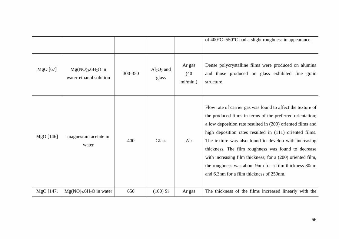
66
of 400°C -550°C had a slight roughness in appearance.
MgO [67]
Mg(NO)3.6H2O in
water-ethanol solution 300-350
Al2O3 and
glass
Ar gas
(40
ml/min.)
Dense polycrystalline films were produced on alumina
and those produced on glass exhibited fine grain
structure.
MgO [146]
magnesium acetate in
water 400 Glass Air
Flow rate of carrier gas was found to affect the texture of
the produced films in terms of the preferred orientation;
a low deposition rate resulted in (200) oriented films and
high deposition rates resulted in (111) oriented films.
The texture was also found to develop with increasing
thickness. The film roughness was found to decrease
with increasing film thickness; for a (200) oriented film,
the roughness was about 9nm for a film thickness 80nm
and 6.3nm for a film thickness of 250nm.
MgO [147, Mg(NO)3.6H2O in water 650 (100) Si Ar gas The thickness of the films increased linearly with the

67
149]
deposition time while the roughness increased. The films
deposited at 650°C from 0.078M solution resulted in
RMS value of about 20-25nm for a deposition time of 32
minutes and 40-45nm for a deposition time of 64
minutes. They also found that inclined substrate
deposition (ISD) resulted in thinner films when
increasing the inclination angle.
ZnO [141]
Zinc acetates i.e.
Zn(CH3CO2).2H2O in
mixture of distilled
water and isopropyl
200-425 Glass Compressed
air
Deposition rate decreased with increasing temperature
due increased rate of re-evaporation. The (002) texture
became more dominant at high temperatures. The film
thickness was found to decrease with increasing the
substrate temperature.
CeO2 [147,
148, 153]
Cerium nitrates i.e.
Ce(NO3)3.6H2O in water200-600
Borosilicate
glass
Ar gas
3 and 10
l/min.
Low flow rates resulted in (111) oriented films in the
temperature range 325°C-450°C. (200) oriented films
were obtained when using high flow rates in the

68
temperature range 450°C-550°C. In the temperature
range between 250°C-450°C, the thickness increased
almost linearly with temperature. In the temperature
range between 450°C-550°C, the thickness slightly
decreased with increasing temperature. The thickness
was also found to increase with increasing the precursor
concentration and the texture improved with increasing
thickness and temperature.
The texture was found to improve with increasing the
temperature but on the expense of roughness. The
thickness was found to increase with temperature up to
450°C then decreased. The thickness of the film
increased with increasing the precursor concentration.
CeO2 [150-
152]
Cerium acetylacetonate
i.e.
Ce(CH3COCHCOCH3)3
in a 50% ethanol / water
450 (100) Si Compressed
air
Appropriate control of the ratio of pulse time to interval
time was necessary for obtaining high texture quality and
greater crystallite size cerium (IV) oxide thin films. The
crystallite size was found to decrease with increasing the
ratio of pulse time to interval time. At large ratios, the

69
generation reaction rate was high and the rate of nuclei
formation exceeded that of the growth of nucleation.
While at low ratios, the growth rate of nucleation
predominated and hence the increase of crystallite sizes
predominated. Therefore, short pulse time and relative
long pulse-interval time could provide enough time to
grow smooth and high density films.
CeO2 [62]
Ce(NO3)3.6H2O in
50% water-ethanol
mixture
350-500 Fused silica -
The best uniform ceria films with nanometric scale
grains (20nm) were prepared at a substrate temperature
of 400°C with 0.5 h annealing of the deposit at 500°C.
At lower spraying temperatures large CeO2 crystallites
have been observed on the film surface along with the
fine grains. When the substrate temperature exceeded
400°C, numerous cracks caused by thermal stresses
appeared in the films.
CeO2 [63]
Ce(NO3)3.6H2O,
CeCl3.7H2O,
in
ethylene glycol
350-500 Β-quartz -
The deposited films were polycrystalline except the ones
deposited from ethylene glycol solution of Ce(NO3)3
which show a preferred orientation along the [100]
direction. The relatively poor XRD patterns of some of

70
the films (produced at higher substrate temperature) were
due to the rather small thickness of the films. The
roughness increased with the increase in film thickness.
Also the higher substrate temperature led to higher rate
of evaporation and accordingly, to higher supersaturation
and bigger number and smaller size of the crystals
formed. For a substrate temperature of 350°C-500°C, the
crystallite size was in the range of 10-60nm.
CeO2 [154]
cerium chloride, cerium
nitrate 300-500 Glass Air
When using magnesium chloride, the films were
amorphous at 300°C. As the substrate temperature was
increased, the films became more crystalline as indicated
by the increase of the (200) peak intensity. A similar
effect was also observed on CeO2 prepared from cerium
nitrate. The films obtained from the chloride solution
showed large grain size and important density of
porosity. However, the morphology aspect of the
surface, for the films prepared from the nitrate solution,
was less pronounced with very small grains and no
pores.

71
CeO2 [155]
Cerium nitrate in a
mixture of methanol and
de-ionised water
400-600
(100) Si,
glass and
Ni tapes
-
The orientation relationships between CeO2 film and Si
substrate were 001CeO2//001Si and 111CeO2//111Si,
however, no distinct alignment was observed in the CeO2
films deposited on glass. The orientation relationships
between CeO2 and Ni substrate were 001CeO2 //001 Ni and
110 CeO2 //100 Ni. However, the intensity of the CeO2
peaks from the phi scan were very low, besides that, they
did not mention if the deposition was made on buffered
Ni or directly on Ni tapes.
In2O3 [140]
Indium chloride in
ethanol-water mixture 300-500 Glass Air
They found that low precursor concentration resulted in
thin and amorphous film. A linear increase in the growth
rate was observed with the increase in the precursor
concentration up to certain limit then it slows down. The
flow rate was found to affect the crystallinity of the
produced films; a flow rate of 15 l/min showed a
well-crystallized phase with uniform surface. They also
found that the smoothness, uniformity and grain size of
the produced films increased with increasing the
substrate temperature up to 380°C and then deteriorates.

72
In2O3 [158]
InCl3 in methanol 200-375
Oxidised
(100) Si
wafers
-
In the lower temperature range (≤300°C) the growth
rates increased with growth temperature because of the
increase in reaction rates of hydrolysis of the InC13
solute molecules. They reach a maximum at about 300°C
and then decreased as the temperature further increased.
The thickness increased with increasing the
concentration and that the growth rate increased with
increasing the flow rate because of the greater amount of
reactant participating in the deposition process. At higher
flow rates the rate of increase of the growth rate was
slower due to the phenomenon of reactant saturation
effect.
In2O3 [159]
Indium chloride in
ethanol-distilled water 425 Glass
Compressed
air
The preferential orientation of the film changed from
(222) to (400) by increasing the temperature. They also
observed a decrease in film thickness with increasing
temperature due to stronger re-evaporation at higher
temperatures.
ZnO [114]
Zinc acetates in water 207-437 Glass Air
The surface morphology and microstructural
characteristics of the films were highly dependant on

73
deposition temperature. A critical temperature was found
to be around 610K (337°C).
SnO2 [160]
SnCl2 in HCl diluted in
methanol 400 Glass -
The preferred orientation of the films varied with film
thickness and that the deposition rate and film thickness
increased linearly with increasing the concentration.
SnO2 [161]
SnCl2-2H2O in HCl
diluted in methanol 400 Glass -
The deposition rate increased with increasing precursor
concentration and the preferred orientation changed from
(211) to (200) by increasing the concentration and
thickness.
SnO2 [162]
SnCl4-5H2O in alcohol 400-900 (100) Si -
Amorphous films were obtained at low deposition
temperatures (<350°C). A (110) and (200) peaks were
obtained between 350°C and 450°C. They also found
that the texture became (200) when the film thickness
increased to more than 160nm.
CdO [163]
Cadmium nitrate in
alcohol 450-550 Glass - Film thickness increased with increasing temperature.
CuO [164] Cu(CH3COO)2 200-300 Stainless
steel Air
The heating temperature was found to have little limited
effect on the particle size and thickness of the films,
which, however, increased significantly by increasing

74
deposition time (from 30 to 60 minutes). However, for
the deposition time of 30 minutes, the thickness was
found to increase with decreasing the deposition
temperature. Besides that, the films obtained with a
deposition time of 30 minutes were rougher than those
obtained with a deposition time of 60 minutes.

75
2.6 ISD deposition of MgO using e-beam evaporation
The basic requirements of a buffer layer are to be biaxially textured with
suitable lattice parameters and non reactive with a HTS layer [167]. Moreover,
biaxially textured MgO can be grown on non-textured metallic tapes by the
inclined-substrate-deposition (ISD) technique [41, 168] using e-beam evaporation
[168-171] for the fabrication of coated superconductor wires [172]. By this method,
the MgO (200) is grown with the c-axis being tilted from the substrate normal due to
the shadowing effect [173-175]. The deposited YBCO film on top of that MgO also
grows with the (00l) being tilted from the substrate normal, which has led to low Jc
values. Higher Jc and Tc values are obtained by growing untilted YBCO films by
depositing YSZ and CeO2 buffers on top of the tilted MgO film [169, 176, 177]. The
biaxial texture is achieved by many techniques ( 2.1.4.1) and for MgO it is achieved
mainly by the inclined substrate deposition (ISD). It was first reported by K.
Hasegawa et al [49, 167, 178] in 1996 to deposit biaxially aligned YSZ films on
untextured Hastelloy (Ni base alloy) tapes; by using an off-axis pulsed laser ablation,
ISD led to in-plane alignment of YSZ films. Later on, in 1999, Bauer et al [179] grew
biaxially aligned MgO buffer on Hastelloy C276 from a sintered MgO target using
e-beam evaporation. In 2000, M.P. Chudzik et al [180] from the Argonne National
Laboratory succeeded in depositing biaxially textured MgO on continuously moving
Hastelloy C tapes by e-beam evaporation and found that the texture improved by
increasing the inclination angle.
Therefore, e-beam evaporation can be used to deposit MgO by the inclined
substrate deposition [173, 174]. By this method, the MgO (200) is grown with the
c-axis being tilted from the substrate normal due to the shadowing effect as can be
seen from the schematic diagram in Figure 2.29 [173-175, 180, 181]. The deposited
YBCO film on top of that MgO also grows with the (005) being tilted from the
substrate normal, which led to low Jc values. M. Bauer et al [179] found that for the
tilted YBCO films, the current can flow in two different directions i.e. in the a-b plane
(in-plane) and along the c-axis which resulted in lower Jc values. Higher Jc and Tc
values were obtained by growing untilted YBCO films by depositing YSZ and CeO2
buffers on top of the tilted MgO film [169, 176, 177].

76
Figure 2.29: Schematic diagram showing the principle of ISD deposition (left) and schematic diagram
showing the growth of crystals truncated by (200) planes (right) [175].
Ralf Metzger et al [173] deposited biaxially textured MgO, as a buffer material,
on Hastelloy C276 by the inclined substrate deposition using e-beam evaporation.
Starting from numerous single crystalline nuclei with random orientation, each
nucleus grew by epitaxial alignment of MgO from the vapour phase. The inclined
direction of incidence of the arriving vapour caused some orientations to grow faster
in height than others. The taller columns can shadow some of their smaller neighbours
resulting in the extinction of the latter. Therefore, MgO (200) grew tilted with respect
to the substrate normal. M.P. Chudzik et al [175] found that the texturing of MgO,
deposited on metal foils, was a selective growth process where the texture improved
with increasing film thickness and with increasing the inclination angle. They found
that the creation of biaxial texture in the MgO film was due to the combined effect of
the cubic equilibrium crystal habit of MgO and columnar self-shadowing. The
columns grew nominally parallel to the substrate normal despite the highly inclined
angle of the atomic flux. The top of such columns were truncated by (200) planes.
Beihai Ma. et al [39, 41, 50, 169, 171, 177, 182, 183] deposited MgO by ISD on
Hastelloy C276 with e-beam evaporation. The ISD MgO films revealed a roof tile
structure and the in-plane texture of the MgO film improved with increasing thickness
and the films became smoother with increasing the thickness. Yttria-stabilised
zirconia (YSZ) buffer layer, ceria cap layer and YBCO films were subsequently
deposited on the ISD-MgO-buffered metallic substrates by PLD. The MgO (200) was
tilted with respect to the substrate normal. However the YBCO films were biaxially
textured with the c-axis parallel to the substrate normal. A sharp Tc of 91K was
obtained. In another study, they found that further improvement in the MgO texture
77
and a decrease in surface roughness were obtained by depositing a homoepitaxial
MgO layer on the ISD MgO layer at elevated temperature and flat angle. The same
group also found that the type of buffer on top of the ISD MgO films affected the
texture of the deposited YBCO films. The use of SrTiO3 (STO) as a buffer layer on
top of the ISD MgO resulted in epitaxial growth of YBCO films with the c-axis tilted
with respect to the substrate normal. The deposition of YBCO directly on the
ISD-MgO resulted also in the growth of YBCO with the c-axis tilted from the
substrate normal. However, when using YSZ and CeO2 instead of STO, a c-axis
untilted YBCO films were obtained. They revealed that CeO2 controls the orientation
of the YBCO films grown on ISD-MgO buffered metal substrates. They also found
that there was an optimal CeO2 thickness (10 nm), above and below that thickness, the
YBCO texture was bad. Similar dependence of the YBCO texture on the CeO2
thickness was found by Méchin et al [95]. Develos et al [165] found that the surface
morphology of CeO2 was changed by changing the thickness. Shi et al [184] found
that the CeO2 growth mode changed on changing the deposition temperature and
thickness i.e. the growth mode was layer-by-layer at 790°C (up to a thickness of
100nm) which gave smooth surfaces and island growth was experienced at 775°C and
805°C (by a thickness of 100nm) and layer-by-layer (up to a thickness of 10nm).
Y Xu et al [174] deposited MgO templates on Hastelloy C276, buffered with
YSZ, in an electron beam (e-beam) evaporation system by inclined substrate
deposition. The MgO in-plane texture was formed by the preferred growth direction
of [11n] // substrate normal and one of the MgO {200} planes rotated to the in-flux
direction. They found that the texture evolved faster and the films were thinner and
rougher, due to the formation of voids and loose structure, at high inclination angles
compared to that at lower inclination angles. They also found that the texture
improved with thickness and with increasing the inclination angle.
Rachel E. Koritala et al [185] deposited biaxially textured MgO films by ISD
using e-beam evaporation on Hastelloy C substrates. They found that the roughness
increased with increasing thickness. High roughness values were also obtained at low
and high inclination angles and the lowest roughness values were obtained for
inclination angles of 20°-55° where the roughness was not affected by the inclination
angle in this range.
In 2002, Balachandran et al [53] grew biaxially textured MgO films by inclined
substrate deposition (ISD), with electron beam evaporation, at deposition rates of

78
20-100 Å/s on Hastelloy C276. The substrate inclination angle was varied between
10° to 70°. Columnar grain structures with roof-tile-shaped surfaces were observed
for the films deposited at room temperature with an inclination angle of 55°. The
films exhibited good biaxial texture. In the same year, Ma et al [40, 50] deposited
MgO by the same method. In order to reduce the surface roughness, a thin layer of
MgO was deposited at 0°. They noticed the same columnar grain structure with MgO
being biaxially textured. Therefore, MgO deposited by ISD is an excellent candidate
for fabrication of high-quality YBCO coated conductors.
2.7 MgO deposition on Si substrates by PLD
Atsushi Masuda et al [186] deposited [100] oriented MgO buffer layers by
pulsed laser deposition on (100) Si substrates using ceramic MgO pellets as the target.
They used an ArF excimer laser operating at wavelength of 193nm for which the
optical absorption coefficient is high in MgO. The fluence used was 7 J/cm2 and the
deposition temperature ranged from 550°C-800°C under 0.13 mbar (~0.1 torr) and
1x10⁻⁷ mbar (7.5x10⁻⁸ torr) O2. (200) oriented films were obtained under 0.13 mbar
and amorphous films were obtained under high vacuum (1x10⁻⁷ mbar or 7.5x10⁻⁸
torr). X. Li et al [187] deposited MgO on Si (100) substrates by PLD, using an energy
fluence of 4 J/cm2, from Mg and MgO targets. High vacuum (5x10⁻⁶ torr) resulted in
amorphous MgO films when using the MgO target, however, Mg targets resulted in
(100) textured MgO films under same sort of vacuum and the strongest MgO peak
was obtained at 650°C. This difference was attributed to different nucleation
processes for the MgO crystals when using different targets; when the Mg atoms were
offered to the substrate surface by using a Mg target, the migration of Mg atoms and
the reaction of Mg with O2 on the substrate surface promote the growth of MgO at the
desired orientation more effectively than when a MgO target was used. Other
researchers deposited MgO films on different substrates using Mg targets under
different conditions [188-190].
2.8 MgO surface optimization for YBa2Cu3O7 (YBCO) thin film
growth and YBCO defects
High temperature annealing was reported to form steps on the MgO substrate
surfaces which favour YBCO deposition by pulsed laser deposition. It was also found
that the annealing controls the production of in-plane orientation of c-axis YBCO

79
films. However, in some cases, YBCO films sputtered on annealed MgO substrates
were found to contain a high density of 45° misoriented grains [191-193].
B. H. Moeckly et al [193] found that annealing of MgO substrates in air or
oxygen to 1100°C-1200°C for 12-24 hours resulted in the formation of a high density
of atomic steps on the substrate surface, and subsequently the deposited YBCO films
were biaxially textured. M. Grant et al [192] annealed (001) MgO substrates in air at
1350°C for 10 minutes to form a series of steps on the surface. They found that the
steps form as a result of lowering the total free energy of the system. Degardin et al
[191] studied the effect of annealing temperature, time and atmosphere on MgO
morphology. The annealing was made at 900°C-1100°C for times of 2-10hrs using air
and pure oxygen. They found that the surface morphology depends on the annealing
conditions. The optimal annealing condition for MgO in terms of the quality of the
deposited YBCO films was to use 1000°C for 5hrs under pure oxygen where they
found that substrate surface reconstruction occurs at this temperature. This resulted in
(001)-oriented terraces bounded by (100)-oriented steps on the MgO surfaces. The
deposited YBCO films exhibited 0° misorientation and high Jc (0.75x10⁶ A/cm2)
compared to the un-annealed samples (0.01x10⁶ A/cm2) and to the samples annealed
under other conditions (0.2 to < 0.75x10⁶ A/cm2).
It is known that MgO is hygroscopic [194]. Simulations made by Walter Langel
and Michele Parrinello [195] revealed that the dissociation of water could proceed
very quickly on MgO stepped surfaces. Thus, the formation of hydroxyl groups or
magnesium carbonates after exposure of MgO to air may reduce the quality of
subsequently deposited films [191, 196]. B. I. Kim et al [196] found that
high-temperature annealing (1000°C) in dry oxygen removed carbon contamination
from degraded MgO substrates stored in moist air for several days.
The effect of storage and humidity on the produced films was studied by
Balkenende et al [116]. They found that MgO layers, deposited by spray pyrolysis
using magnesium acetates as a precursor, were easily degraded by air while in storage.
This is caused by the reaction of magnesium oxide with water and carbon dioxide in
air and form a surface layer of magnesium carbonate and magnesium hydroxide.
However, heating the contaminated layer briefly at a temperature of 450°C in air was
sufficient to regenerate the MgO surface [116].
J Du et al [197, 198] found that MgO substrates, after weeks of exposure to
laboratory environment, were degraded by the formation of hydroxyl groups,

80
carbonates and other possible carbon compounds. YBCO films grown on these
contaminated or degraded MgO substrates showed an increased degree of 45°
in-plane grain misorientation, which reduces the film critical current density from
3x10⁶ A/cm2 (for a fresh MgO substrate) to 0.005x10⁶ A/cm2. The effect of annealing
at 760°C in mixed 1:15 oxygen : argon gas at pressure of 50 Pa was studied by XPS.
The main O 1s peak at 529.5 eV is due to the original substrate MgO oxygen atoms
and the shoulder at a higher binding energy (HBE) in the range 531–532 eV is due to
oxygen of other oxygen-bearing compounds. It is well established in the literature that
hydroxylation of MgO (i.e formation of (Mg(OH)2) causes the O 1s core level to shift
to a higher binding energy by about 2.2 eV or sometimes 3eV [199-201]. J Du et al
found that annealing improved the surface quality by removing many contaminants,
mostly hydroxides Mg(OH)2 and carbonates MgCO3. Subsequent YBCO films grown
on MgO with this pre-treatment showed perfect grain alignment and high critical
current densities (2.4x10⁶ A/cm2). Fares Khairallah and Antonella Glisente [202] used
XPS to characterize nanoscale magnesium oxide. O 1s and Mg 2P were used to
differentiate between MgO and Mg(OH)2. Mg 2P is used to confirm the presence of
Mg as an oxide or hydroxide which occurs at 49.3-49.5eV. The O 1s reveals the
presence of Mg and confirms if present as MgO (529.6-529.8eV) or as hydroxide i.e.
as Mg(OH)2 (531.1-531.3eV). Similar results were found by others [201, 203, 204].
Defects in YBCO films have a great influence on the superconducting
properties and on the surface smoothness and some of them will be mentioned here.
Grain boundary misorientation was found to affect the superconducting properties. D.
T. Verebelyi et al and Z. G. Ivanov [205, 206] found that the critical current density
reduced exponentially with increasing the misorientation angle beyond 4° (~ 4x10⁶
A/cm2) up to 40° (~ 1x10² A/cm2). The dependence of the critical current density on
the misorientation angle was also found by others [197, 198, 207].
T.J. Jackson et al [208] deposited YBCO films on STO (001) substrates by
pulsed laser deposition. They found that the films frequently exhibited holes which
were correlated with the incidence of epitaxial yttria (Y2O3) precipitates within the
film and with suppression of twining of YBCO films. All the films have a
superconducting transition onset temperature of about 90K. The films with holes,
which are as deep as the film thickness, have wide transition temperatures of about
7K, while films with shallow holes have transition widths less than 1K. They also
found that it is still unclear why a minority of films prepared under apparently

81
identical conditions can be obtained without holes and precipitates. R. Krupke et al
[209] related the formation of holes in YBCO film deposited on LaAlO3 (LAO) to
Y2O3 as well. The formation of such Y2O3 inclusions was also observed by others
[210, 211]. However, Develos et al [212] related the formation of the pores in YBCO
films deposited on LAO substrates to yttrium rich composition (BaY2O4). This
off-stoichiometry in the composition of the films was attributed to the scattering of the
ablated species with the oxygen ambient. They found that nucleation and enlargement
of the barium yttrium oxide phase obstructs the YBCO growth and eventually caused
pore formation.
The effect of film thickness on the critical current density of YBCO films on
CeO2/YSZ/CeO2 buffered rolling assisted biaxially textured Ni substrates was studied
by K. J. Leonard et al [213]. They found that the critical current density decreased
with increasing the film thickness (~ 2.5x10⁶ A/cm2 for a film thickness of ~ 0.2µm
and ~ 0.5x10⁶ A/cm2 for a film thickness of ~ 3µm ), due to the formation of more
randomly oriented grains in the upper portion of the YBCO film surface, resulting in
less cube texture. In addition, an increase in mismatch across the boundaries of the
c-axis grains with increasing time during deposition, along with the development of
BaCeO3 and Y2BaCuO5 phases at the YBCO/CeO2 buffer interface, contributed to the
degradation of film properties where misoriented YBCO growth occurs above such
phases.
MgO deposition by PLD requires high vacuum and high fluence. PLD and other
depositing techniques are considered relatively expensive compared to spray
pyrolysis. Therefore, in sections 2.5- 2.7, a literature survey was made in an attempt to
put the main key factors in depositing MgO and other films by spray pyrolysis and by
other deposition techniques available for the reader. The effect of the main depositing
variables on the properties of the produced films was mentioned. However, it is to be
mentioned that not many reports were found for MgO deposition by spray pyrolysis.
It was found that, for MgO deposition by spray pyrolysis on different ceramic
substrates from different precursors, the substrate temperature affects texture
evolution and surface morphology of the deposited films and that the properties of
films depend on the used substrate. The texture of films was found to develop with
thickness and that the thickness either increased or decreased with increasing
temperature but increased with increasing the deposition time. The texture was also
found to improve with increasing precursor concentration; however, it was found in
82
some reports that there is a concentration limit above and below which the texture
deteriorates. Flow rate was found to affect the preferred orientation for MgO and
other films. For MgO films deposited by other techniques it was found that the films
grew with (100) orientation irrespective of the substrate temperature but the texture
was found to improve and the roughness deteriorates with increasing temperature.
However, no reports were found for MgO deposition on metallic substrates;
consequently, the effects of different depositing variables need to be investigated. In
addition, no reports were found for YBCO deposition on top of the spray pyrolysed
MgO to evaluate its performance.
For other films deposited by spray pyrolysis it was found that the thickness
increased and the texture improved with increasing precursor concentration and
increasing temperature. Others found that amorphous films were obtained at low
temperature and low thicknesses. It was found that pulse time to interval time affects
the quality of the texture. Flow rate was found to affect the crystallinity of the
produced films. Smoothness, uniformity and grain size of the produced films were
found to increase with increasing the substrate temperature up to certain temperature
and then deteriorate. Film properties were found to change by changing the substrate
or precursor even when using the same deposition conditions. The film thickness was
found to decrease with increasing temperature. However, others found that the
temperature have limited effect on the thickness.
ISD deposition of MgO was done mainly by e-beam evaporation to deposit
biaxially textured MgO films on polycrystalline Hastelloy C276 substrates. This is
important for the subsequent deposition of high Jc YBCO superconducting films. By
this method, the MgO (200) is grown with the c-axis being tilted from the substrate
normal due to the shadowing effect and this led to YBCO films with low Jc and Tc
values. Texture was found to improve with increasing thickness and with increasing
inclination angle. However, no reports were found for MgO deposition by ISD using
spray pyrolysis.
Annealing of the MgO substrates was found to be beneficial to control the
in-plane texture of the subsequent YBCO films by the formation of atomic steps on
the surface which lowers the total free energy of the system. This approach was not
found in the literature for MgO films deposited by spray pyrolysis.

83
3 Experimental details
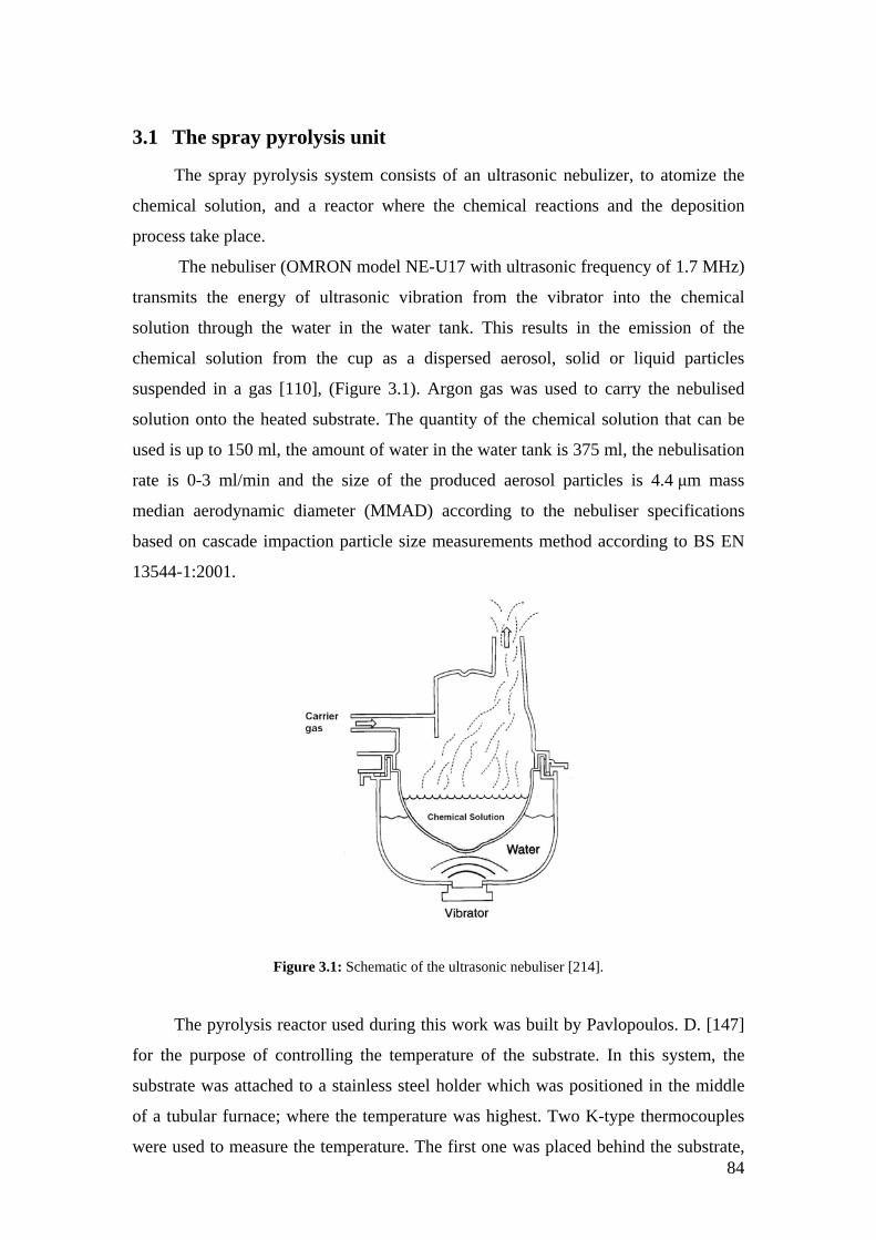
84
3.1 The spray pyrolysis unit
The spray pyrolysis system consists of an ultrasonic nebulizer, to atomize the
chemical solution, and a reactor where the chemical reactions and the deposition
process take place.
The nebuliser (OMRON model NE-U17 with ultrasonic frequency of 1.7 MHz)
transmits the energy of ultrasonic vibration from the vibrator into the chemical
solution through the water in the water tank. This results in the emission of the
chemical solution from the cup as a dispersed aerosol, solid or liquid particles
suspended in a gas [110], (Figure 3.1). Argon gas was used to carry the nebulised
solution onto the heated substrate. The quantity of the chemical solution that can be
used is up to 150 ml, the amount of water in the water tank is 375 ml, the nebulisation
rate is 0-3 ml/min and the size of the produced aerosol particles is 4.4 μm mass
median aerodynamic diameter (MMAD) according to the nebuliser specifications
based on cascade impaction particle size measurements method according to BS EN
13544-1:2001.
Figure 3.1: Schematic of the ultrasonic nebuliser [214].
The pyrolysis reactor used during this work was built by Pavlopoulos. D. [147]
for the purpose of controlling the temperature of the substrate. In this system, the
substrate was attached to a stainless steel holder which was positioned in the middle
of a tubular furnace; where the temperature was highest. Two K-type thermocouples
were used to measure the temperature. The first one was placed behind the substrate,

85
which is going to represent the deposition temperature in this work, i.e., the substrate
temperature, and the other one was placed in the mid-height of the furnace close to the
wall. The nozzle diameter was 1 cm and the substrate to nozzle distance (SND) was
fixed at 7 cm. Figure 3.2 and Figure 3.3 show a schematic and an image of the used
spray pyrolysis system, respectively.
Figure 3.2: Schematic of the spray pyrolysis reactor [147].
Figure 3.3: A photograph of the spray pyrolysis system showing, from left to right, the gas flow meter,
the thermocouple, the temperature controller, the tubular furnace and the ultrasonic nebuliser.

86
MgO deposited by inclined substrate deposition (ISD) using e-beam evaporation
was found to be an excellent candidate for fabrication of high-quality YBCO coated
conductors (section 2.5). Therefore, ISD was investigated using spray pyrolysis as no
reports were found addressing this issue. Inclined substrate deposition (ISD) was
made by inclining the substrate relative to the aerosol flow as can be seen in Figure
3.4.
Figure 3.4: Schematic of the ISD setup.
During the spray pyrolysis deposition process, the temperature of the holder was
observed to drop by 10°C-30°C. Therefore, the ratio of pulse time to interval time was
set at 1 to 7, i.e. 15 seconds deposition after which the gas flow was turned off; 105
seconds needed for the heater to stabilise to the set temperature. This process was
repeated for any required period of time. The furnace was then turned off and the
sample was left to be furnace cooled down to room temperature. The parameters
which were fixed for all of the depositions during this work are summarised in Table
3.1 while Table 3.2 lists the examined parameters.
Table 3.1: Deposition parameters that are kept fixed during deposition.
Deposition parameter Deposition conditions
Argon flow rate 5,10 and 15 l/min
Pulse time 15 seconds
Interval time 105seconds
Substrate-nozzle distance 7 cm
Nozzle diameter 1 cm
Precursor solvent Distilled water
Cooling of samples Furnace cool in atmosphere
Heating rate 3°C/min.
Nozzle: aerosol flow
Substrate α:Inclination angle
Substrate holder

87
Table 3.2: The examined deposition parameters.
Substrate temperature Type of the substrate
Type of the precursor
(nitrate, acetate) Substrate inclination angle
Concentration of solution Deposition time
3.1.1 The deposition substrates
MgO was deposited on different substrates i.e. on (100) oriented Si single
crystal wafers (10mm X 10mm X 340µm), on Ni- 5at%W (10mm X 10mm X 100µm)
rolling assisted biaxially textured substrates (RABiTS) and on polycrystalline
technical substrates which include wrought 310-austenitic stainless steel and
Hastelloy C276 (10mm X 10mm X 2mm). The RABiTS and the technical substrates
were mechanically polished down to a roughness of about 2-5nm.
Substrates were cleaned using acetone (CH3COCH3), then ethanol
(CH3CH2OH), in an ultrasonic bath for a period of 10 min each. They were then dried
with Argon gas.
3.1.2 MgO film deposition
The MgO buffer or template layer was deposited by the Spray Pyrolysis
technique using magnesium nitrate [Mg(NO3)2.6H2O] or magnesium acetate
[Mg(CH3COO)2.4H2O] as precursors. The required concentrations were made by
dissolving a specific amount (in grams) of each precursor in distilled water (e.g. 2
grams of each precursor were dissolved in 100ml of distilled water to give a
concentration of 0.093M of magnesium acetate and 0.078M of magnesium nitrate,
respectively). The decomposition temperature of the precursors was measured by
thermogravimetrical analysis (TGA) which will be explained in section 3.3.1.
3.2 Pulsed laser deposition (PLD)
The pulsed laser deposition (PLD) was used, as a well established route to high
quality films [19, 20], to deposit the superconducting YBa2Cu3O7 (YBCO) layer on
the MgO-buffered substrates. This was done to evaluate the MgO performance as a
buffer, although spray pyrolysis of the YBCO layer should also be a possibility in the

88
future [24, 25, 69, 174, 175]. CeO2 was also deposited by PLD on top of the
MgO-buffered substrates in an attempt to improve the in-plane texture of YBCO.
For YBCO deposition by PLD ( using YBCO target with 99.9% purity bought
from PI-KEM), an excimer laser (Lambda Physik, LPX 300) with a wavelength of
248 nm was used. The laser was focused on a rotating YBCO target with a raster
movement at an energy density of 2 and 2.75 J/cm2 (the energy of the beam was
measured inside the deposition chamber prior to each deposition and the target was
ground to a smooth finish before each deposition). Substrates were mounted on a
heatable sample stage with silver paste, the chamber was then evacuated, the target
was then cleaned and conditioned with a 1000 laser pulses under vacuum with a
shutter being positioned over the substrate. The substrate was then heated to 780°C at
a rate of 20°C/min. The distance between the target and the substrates was 56 mm,
and an oxygen background pressure of 450 mtorr (0.6 mbar) was employed during the
deposition. 5000 pulses at pulse repetition rate of 4 Hz were employed for YBCO
deposition. Cooling of the substrates was at a rate of 10°C/min under an oxygen
background pressure of 525 torr (0.7 bar) which was introduced into the chamber over
8 minutes while maintaining the substrate temperature. Other deposition parameters
were used as well and will be mentioned when necessary, however, 1000 pulses at
pulse repetition rate of 2 Hz was employed for CeO2 deposition. Figure 3.5 and Figure
3.6 show a schematic of the PLD system and an image of the used PLD machine,
respectively.
Figure 3.5: Schematic of the PLD system [215].
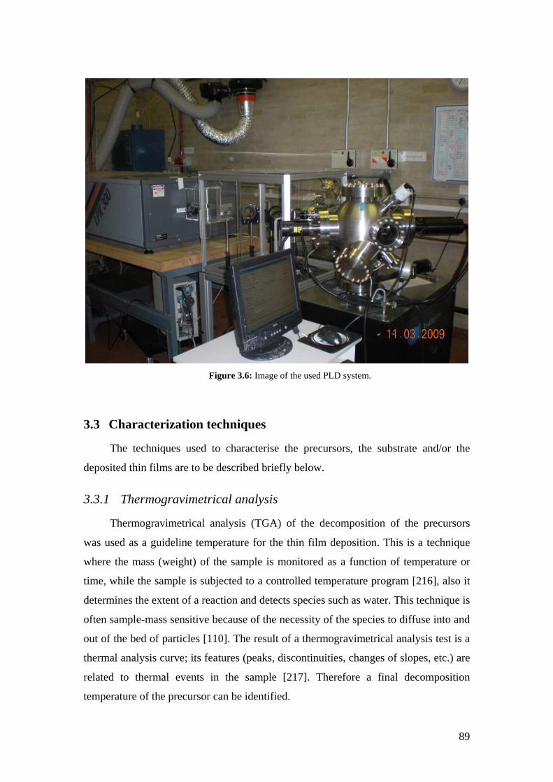
89
Figure 3.6: Image of the used PLD system.
3.3 Characterization techniques
The techniques used to characterise the precursors, the substrate and/or the
deposited thin films are to be described briefly below.
3.3.1 Thermogravimetrical analysis
Thermogravimetrical analysis (TGA) of the decomposition of the precursors
was used as a guideline temperature for the thin film deposition. This is a technique
where the mass (weight) of the sample is monitored as a function of temperature or
time, while the sample is subjected to a controlled temperature program [216], also it
determines the extent of a reaction and detects species such as water. This technique is
often sample-mass sensitive because of the necessity of the species to diffuse into and
out of the bed of particles [110]. The result of a thermogravimetrical analysis test is a
thermal analysis curve; its features (peaks, discontinuities, changes of slopes, etc.) are
related to thermal events in the sample [217]. Therefore a final decomposition
temperature of the precursor can be identified.

90
In this work, 7 mg of each precursor was placed in an alumina crucible. The
TGA analysis was performed in 75cm3/min flow of Argon from 25°C to 750°C at a
constant heating rate of 10°C/min. using a NETZSCH apparatus model STA 449 C.
3.3.2 X-ray diffraction (XRD)
For a diffraction to occur, the Bragg law must be satisfied i.e.:
nλ = 2dsinθ (Eq. 3.1)
where n is an integer and called the order of diffraction, λ is the wavelength of an
incident monochromatic X-ray beam, d is the interplanar spacing and θ is called the
Bragg angle, the angle between the incident X-ray beam and the particular crystal
plane under consideration. Figure 3.7 shows a schematic of the X-ray
diffractometer [218].
Figure 3.7: Schematic of X-ray diffractometer [218].
In θ-2θ scans, a rotation of the detector through 2θ degrees is automatically
accompanied by a rotation of the sample through θ degrees [218]. In this work this
was carried out using a two circle Philips machine with a monochromatic Cu Kα
radiation having a wavelength of 1.54Å. Phase identification and crystal structure
information can be obtained from such a scan. Moreover, qualitative information

91
about the out-of-plane texture can be obtained as well. However, for quantitative
information, rocking curves analysis (ω scan) is required. This scan is similar to the
θ-2θ scan mode but the movement of the sample and the detector is decoupled, where
a sample at a position θ is rocked about the diffractometer axis within a range (θ+Δθ)
(Figure 3.7) while the detector is kept fixed at the corresponding 2θ. The full width at
half maximum (FWHM) can then be measured to characterise the quality of the
crystal.
Qualitative in-plane and out-of-plane information can be obtained by
performing a pole figure measurement scan. The pole figure is a stereographic
projection, with a specified orientation relative to the specimen, that shows the
variation of pole density with pole orientation for a selected set of crystal planes
[218]. The pole figure is often plotted in polar coordinates consisting of the tilt and
rotation angles with respect to a given crystallographic orientation. A pole figure scan
is performed at a fixed θ and 2θ and consists of a series of in-plane rotation (φ
rotation) around the center of the sample, i.e. a rotation of the sample in its own plane
about an axis normal to its surface, at different tilt (ψ) angles [218, 219] as illustrated
in Figure 3.8.
A 3-circle Hiltonbrooks X-ray diffractometer with Cu Kα radiation having a
wavelength of 1.54Å was used for the pole figure scan measurements.
Pole figure measurements give qualitative information about the in-plane
texture. For quantitative information, a phi (φ) scan is needed. The scan is performed
by rotating the sample 360° through φ at a fixed (ψ, θ and 2θ) which belongs to a
plane satisfying the Bragg condition. The in-plane texture quality is then evaluated by
measuring the FWHM.
The rocking curve and the φ scans were performed using a four circle Siemens
D5000 diffractometer with Cu Kα radiation having a wavelength of 1.54Å.

92
Figure 3.8: Schematic showing the φ and ψ rotations during pole figure measurements [218].
3.3.3 Scanning electron microscopy (SEM)
Scanning electron microscopy is one of today’s most important material
microstructural characterization techniques. It produces images over a wide range of
magnification; additionally, the variety of electron induced signals can yield a great
deal of morphological, textural and chemical information about a specimen.
One of the scanning electron microscopy components is the electron gun which
produces a focused beam of electrons that strikes the specimen for the production of a
high resolution image, where an electrical potential is established between a
negatively charged filament (cathode) and a positively charged plate (anode). This
electrical potential is referred to as the accelerating voltage. The simplest and the
widely used electron gun is the thermionic emission gun (conventional hairpin-shaped
tungsten and fine-tipped LaB6 filaments) where electrons are emitted from a heated
filament and then accelerate towards the anode.
The image in a scanning electron microscope is improved (better resolution) by
reducing the filament tip diameter. This was achieved in the field emission gun, which
uses a short piece of specifically oriented, single crystal tungsten wire electrolytically
etched to a very sharp tip, where the electrons are drawn by an electrical field. This
results in enhanced electron emission relative to the thermionic sources.
The scanning electron microscope utilizes a focused beam of high energy
electrons that systematically scans across the surface of the specimen. The interaction
of the beam with the specimen produces a large number of signals at or near the
specimen surface. Figure 3.9 shows the possible signals generated by the primary

93
electron beam-specimen interaction in the scanning electron microscope. These
interactions include low energy electrons, termed secondary electrons. The low
energy of secondary electrons (due to inelastic scattering and can only escape near the
surface of a specimen) makes them a conveniently collected signal for scanning
electron microscopy since they can be easily drawn to a positively biased detector
system. The electron signal is eventually converted to an electronic signal which is
portrayed on cathode ray tube (essentially a television screen) giving information
about the surface structure; this also provides high resolution imaging of fine surface
morphology, as the intensity of secondary electrons reaching the detector is
influenced by the surface topography. The interactions also include high energy
electrons termed backscattered electrons, as a result of elastic scattering, and can
escape from greater depths within the sample, so giving topographical information but
not as accurately resolved as for secondary electron imaging. It also provides image
contrast as a function of elemental composition i.e. atomic number contrast. X-rays
are generated much deeper below the sample surface and are used for chemical
analysis [220-222].
Figure 3.9: Electron beam-specimen interaction [220].
The scanning electron microscope may be facilitated by microanalytical tools
which include wavelength dispersive spectroscopy (WDS) and energy dispersive
spectroscopy (EDS). It may also be facilitated by the electron backscattered
diffraction (EBSD) texture measurement tool. Figure 3.10 shows a JEOL JSM-7000F
with a field emission gun scanning electron microscope, facilitated with EDS, WDS
and EBSD, which was used during this work for high resolution images (e.g. for

94
thickness measurement of a thin film) and texture analysis. JEOL JSM-6060LV with a
tungsten thermionic gun facilitated with EDS was also used for low magnification
images and chemical microanalysis.
Figure 3.10: A JEOL 7000 scanning electron microscope.
3.3.3.1 Energy dispersive spectroscopy (EDS)
X-rays are one of the most widely used products of the electron beam-sample
interaction. Analytical electron microscopy is accomplished by the coupling of an
X-ray analysis device (EDS) with a scanning electron microscope. The analysis can
be performed quickly and most importantly it is non-destructive to the sample [221].
The sample consists of atoms, and the atoms consists of a central nucleus
surrounded by electrons lying in various shells (K, L, M,…). If an electron from an
electron beam hitting the sample has sufficient kinetic energy, it can knock an
electron out from the K shell, leaving the atom in an excited, high energy state. One of
the outer electrons immediately falls into the vacancy in the K shell, emitting energy
in the process, and the atom is once again in its normal energy state. The energy
emitted is in the form of radiation of a definitive wavelength and is, in fact,
characteristic K radiation. The K shell may be filled by an electron from the L or M

95
shells giving rise to Kα and Kβ, respectively. L characteristic lines originate in a
similar way [223] and so on.
The X-rays produced from the electron beam-sample interaction have energies
(wavelengths) characteristic of the elements in the sample. These wavelengths are
separated by the EDS on the basis of their energies by means of a Si(Li) counter and a
multichannel analyzer (MCA).
When an X-ray strikes the semiconductor Si(Li) counter, electrons in the crystal
each absorb a given amount of energy. The higher the energy of the X-ray, the higher
the number of excited electrons. This excitation creates free electrons in the
conduction band and free holes in the valence band, and if a high voltage is
maintained across opposite faces of the silicon crystal, the electrons and holes will be
swept to these faces, creating a small pulse in the external circuit proportional in
height to the energies of the incident beam. The MCA then sorts out the various
pulses heights which are then plotted as intensity vs. energy (KeV) [221, 223]. Figure
3.11 is a schematic of the energy dispersive spectrometer.
Figure 3.11: Schematic of the energy dispersive spectrometer [223].
It is to be mentioned that the EDX is a semi-quantitative measurement tool
especially when dealing with light elements like magnesium and oxygen. The EDX
was used in this work to give a rough indication of the amount of the elements
present. Besides that, the EDX detector used was not windowless which may also
affect the accuracy of the semi-quantitative measurements.
3.3.3.2 Electron backscattered diffraction (EBSD)
The ability to obtain microstructure-level information implies that the probe
size formed by X-rays or electrons must be smaller than the size of the microstructural

96
units themselves. Therefore, this rules out X-ray diffraction as an experimental tool
for microstructure measurements. Electrons are ideal for combined microstructural /
crystallographic studies and TEM was the major technique used for such work. Since
then, a more convenient SEM-based technique for microstructure has been developed,
known as electron backscattered diffraction.
Electron Backscatter Diffraction (EBSD) is a technique which allows
crystallographic information to be obtained from samples in the SEM. In EBSD a
stationary electron beam of electrons is directed onto a tilted crystalline sample; a tilt
of 70° from the horizontal so the angle between the incident electron beam and the
specimen surface is 20° to optimise both the fraction of escaped backscattered
electrons scattered from the sample and the contrast in the diffraction pattern. The
electrons undergo various interactions with the atoms in the crystal lattice and some of
the electrons emerge from the sample. If a fluorescent phosphor screen is placed
close to the sample (Figure 3.12) a pattern is formed on the screen because the
intensity of the emerging electrons varies slightly with direction. This pattern is
called a diffraction pattern which is characteristic of the crystal structure and
orientation of the sample region from which it was generated.
Figure 3.12: An image showing a tilted sample and a phosphorous screen in SEM chamber [224].

97
The mechanism by which the diffraction patterns are formed is as follows: the
atoms in the material inelastically scatter a fraction of the electrons with a small loss
of energy to form a divergent source of electrons close to the surface of the sample.
Some of these electrons are incident on atomic planes at angles which satisfy the
Bragg equation. Since diffraction of the electrons through the Bragg angle is
occurring in all directions, these electrons are diffracted to form a set of paired large
angle cones corresponding to each diffracting plane. When used to form an image on
the fluorescent screen the regions of enhanced electron intensity between the cones
produce the characteristic Kikuchi bands of the electron backscatter diffraction pattern
(Figure 3.13).
Figure 3.13: EBSD geometry [224].
The diffraction pattern can be used to measure the crystal orientation, measure
grain boundary misorientations as it can characterise the boundary by the difference in
orientation on either side of the boundary, discriminate between different materials,
and provide information about local crystalline perfection. The symmetry and
appearance of the diffraction pattern is related intimately to the crystal structure at the
point where the beam meets the sample. If the crystal rotates (in other words its
orientation changes) the diffraction pattern will be seen to move. If a different type of
material is placed under the beam, the diffraction pattern will change completely. So
the diffraction pattern can be used to measure crystal orientations and to identify
materials. When the beam is scanned in a grid across a polycrystalline sample and the
crystal orientation measured at each point, the resulting map will reveal the

98
constituent grain morphology, orientations, and boundaries. This data can also be used
to show the preferred crystal orientations (texture) present in the material, for
example, as pole figure.
Because EBSD measures crystal orientation, and hence used to analyse the
sample texture, then EBSD is complementary to the standard method of measuring
texture using X-ray diffraction. However, EBSD goes further because it can relate the
texture (or textures) present to the microstructure of the material. In addition, textures
which vary from place to place in a sample can be studied easily. The way in which
textures develop can be studied at the level of the microstructure with EBSD [224,
225].
3.3.4 Atomic force microscopy (AFM)
Scanning probe microscopy (SPM) consists of a family of microscopy forms
and the primary two are scanning tunnelling microscopy (STM) and atomic force
microscopy (AFM) which also called scanning force microscopy (SFM).
Since its inception in the mid-1980s, SPM has become a very well-accepted
technique for characterizing surfaces and interfacial processes with nanometer-scale
resolution and precision.
There are three modes of AFM i.e., contact mode AFM, non contact mode AFM
and tapping mode AFM. In this work the contact mode was adopted.
Contact mode AFM operates by scanning a tip (with a nominally atomically
sharp tip, typically pyramidal in shape, which is mounted on the underside of an
extremely sensitive cantilever) across the sample surface while monitoring the change
in cantilever deflection with a split photodiode detector. Precise control over the
tip-sample separation distance is what provides the AFM (SPM) technique with its
high spatial resolution. One can then generate a surface contour map that reflects
relative differences in interaction intensity as a function of surface position.
The tip contacts the sample surface and a feedback loop maintains a constant
deflection between the cantilever and the sample by vertically moving the scanner at
each (x, y) data point to maintain a "setpoint" deflection (Figure 3.14). By
maintaining a constant cantilever deflection, the force between the tip and the sample
remains constant. The force is calculated from Hooke's Law: where
F = –kx (Eq. 3.2)
F = Force

99
k = spring constant
x = cantilever deflection.
Spring constants usually range from 0.01 to 1.0 N/m, resulting in forces ranging
from nN to μN in an ambient atmosphere. The distance the scanner moves vertically
at each (x, y) data point is stored by the computer to form the topographic image of
the sample surface. Operation can take place in ambient and liquid environments.
Figure 3.14: Schematic of the contact mode AFM [226].
The roughness of the film can be calculated from the AFM image. The Root
Mean Square (RMS) Roughness is the standard deviation of the Z values within a
given area and is given by [226, 227]:
RMS = N
ZZN
iavei∑
=
−1
2.)(
(Eq. 3.3)
Zave. : is the average Z value within the given area.
Zi: is the current Z value.
N: is the number of points within a given area.
The atomic force microscope used in this study was a NanoscopeR IIIa (Digital
Instruments, DimensionTM 3100, Veeco Metrology group). Contact mode AFM was
employed at ambient conditions using silicon nitride probes with a nominal tip radius

100
of curvature of 20 nm and spring constant of 0.12N/m. A scan rate of 1 Hz was
employed.
3.3.5 AC susceptibility
There are two classic ways to define superconductivity, one involving the
property of zero resistance and the other based on perfect diamagnetism, i.e. AC
susceptibility, which became popular with the advent of high temperature
superconductivity. In this test magnetisation currents are induced in the sample, by the
application of a small varying magnetic field (HAC) with the aid of a primary coil, and
the flux variation due to the sample is picked up by a sensing (pickup) coil
surrounding the sample, the resulting magnetic moment or susceptibility induced in
the coil is detected by a lock-in amplifier which also separates the χ/ and χ//. Figure
3.15 is a schematic of the AC susceptibility apparatus used in this work.
Lock-in amplifierAC source
Temperature controllerComputer
CryostatPrimary
coilPickup
coil
Balance pickup coil
Balance primary coil
Sample
Lock-in amplifierAC source
Temperature controllerComputer
CryostatPrimary
coilPickup
coil
Balance pickup coil
Balance primary coil
Sample
Figure 3.15: Schematic of AC susceptibility apparatus.
Figure 3.16 shows the real (χ/) and the imaginary (χ//), also called the first
derivative, susceptibilities. The point at which the first derivative reaches its
maximum value could be selected as defining Tc. The width ΔT between the points
where the first derivative curve is half of its maximum value, is a good quantitative

101
measure of the width of the transition. The figure also shows the definition of the Tc
onset and the Tc midpoint.
The susceptibility measurements determine the magnetic state of the entire
sample, and also give a better indication of the extent to which the sample has
transformed to the superconducting state. On the one hand, χ/ gives quantitative
expression for the amount of magnetic flux penetration into the sample; χ/ = -1 for a
complete Meissner expulsion and χ/ = 0 for a full flux penetration. On the other hand,
χ// = 0 in the superconducting state and <1 in the mixed state. When χ// >1 then it
reflects AC losses. This is based on SI units, where numerical results must be
corrected for any sample demagnetising factor [228-233].
20 40 60 80 100 120
TC (midpoint)
TC (onset)
ΔT
ΔT
Temperature (K)
χ/ , χ// (a
. u.)
χ/ real Susceptibility χ// Imaginary Susceptibility
Figure 3.16: χ/ and χ// for YBCO deposited on MgO single crystal with a Tc onset of 90.2K.
The volume magnetic susceptibility (χ) is defined by the relationship:
χ = dM / dH (Eq. 3.4)
where in SI units:
M: is the magnetization of the material (the magnetic dipole moment per unit volume)
measured in Amp/m.
H: is the magnetic field strength also measured in Amp./m [232, 234].

102
3.3.6 X-ray photoelectron spectroscopy (XPS)
XPS is a surface chemical analysis technique based on the binding energies of
the electrons. Electrons are emitted from a metallic surface after the absorption of
energy from electromagnetic radiation, such as X-rays, having a frequency above a
certain threshold frequency (typically visible light). The emitted electrons can be
referred to as photoelectrons. In an XPS experiment electrons are photoionized from
the core levels by X-rays. The surface is irradiated with photons from a soft X-ray
source, most commonly Al Kα (1486.6eV) but also Mg Kα (1253.6eV) is used as
well. By the law of conservation of energy, the electron absorbs the energy of the
photon and if sufficient, the electron can escape the material with a finite kinetic
energy. A single photon can only eject a single electron as the energy of one photon
can only be absorbed by one electron. The cornerstone of XPS is the measurement of
the kinetic energy Ek of the outgoing electrons. This energy is related to the electron
binding energy EB, according to the basic XPS equation which was first made by
Rutherford, and was then modified to:
EK = hυ - EB (Eq. 3.5)
where EK is the kinetic energy of the ejected photo-electron, hυ is the incident photon
energy and EB is the electron binding energy [235-237].
From those binding energies, the state of a specific element can be determined, i.e.
present as an oxide, hydroxide, carbonate…etc.
In this work, the XPS spectra were recorded with a standard Mg Kα source (20
pass energy, 0.1 step, and 0.1 seconds per step for the detailed spectra) using XPS VG
Scientific ESCALAB MKII spectrometer with a spatial resolution of 100μm.

103
4 Spray pyrolysis of MgO on silicon single crystals
using magnesium nitrate as a precursor

104
4.1 Introduction
In this chapter Si single crystals were used for the optimization of the spray
pyrolysis parameters for further deposition on RABiTS and polycrystalline metallic
substrates which will be presented in the following chapters. In addition to that they
have been used due to their low cost. The deposition of MgO thin films by spray
pyrolysis, on (100) oriented silicon (Si) single crystal wafers which has a cubic
diamond structure [223], will be introduced using magnesium nitrate as a precursor.
Before the deposition, the wafers (330µm thick) were cut into 10mm x10mm and then
cleaned in acetone, then ethanol for 10 minutes each in an ultrasonic bath, then dried
with Ar gas. A pulse time to interval time of 1:7 was applied and the deposition time
was 32 minutes. The used Ar flow rate was 10 l/min.
To evaluate the performance of the MgO films, YBCO was deposited by PLD
on top of MgO films deposited by spray pyrolysis on Si and on top of MgO films
deposited by PLD on Si. Therefore, YBCO deposition parameters were first optimised
by depositing YBCO by PLD on MgO single crystals.
Thermal decomposition of the precursor (was used as a guideline temperature
for the thin film deposition) was presented, the effect of the precursor concentration,
substrate temperature and inclination angle on the quality of the spray pyrolysed MgO
films on Si were all investigated. In addition to that, MgO was deposited by PLD on
Si to compare the produced films with those deposited by spray pyrolysis.
It is to be mentioned that X-ray scans for the MgO films deposited by spray
pyrolysis on Si detected only MgO (200) peaks from the MgO films. Therefore, we
could not quantify the level of texture as no other peaks were detected to reference to.
Accordingly, it was assumed that an increase in the intensity of MgO (200) peak
reflects an improvement in texture.
4.2 Thermal decomposition of the nitrate precursor
Before depositing MgO by spray pyrolysis, a thermogravimetrical analysis
(TGA) of the decomposition of the nitrate precursor was used as a guideline
temperature for the thin film deposition. For this purpose, a sample of magnesium
nitrate hexahydrate, Mg(NO3)2.6H2O, with a mass of 7 mg was placed in an alumina
crucible. The thermogravimetric (TGA) analysis was performed in a flow of Argon

105
from 25°C to 750°C. The TGA measurement was performed at a constant heating rate
of 10°C/min. Figure 4.1 shows the TGA curve for the tested Mg(NO3)2.6H2O sample.
0 100 200 300 400 500 600 700 8000
20
40
60
80
100
TG (w
eigh
t los
s %
)
Temperature / oC
Figure 4.1: TGA curve for Mg(NO3)2.6H2O.
The decomposition of Mg(NO3)2.6H2O takes place in three steps as can be seen
from Figure 4.1, the first two are dehydration and the third one is the decomposition
of anhydrous Mg(NO3)2 to MgO, 121 O2 and 2NO [238]. The decomposition finished
at about 500°C which is close to that obtained by Migdal [238] under the same
conditions. He found that the decomposition finished at 770K (496.8°C).
It was found that storage and humidity degrades the MgO films by the
formation of magnesium hydroxide [116]. However, heating the contaminated layer
briefly at a temperature of 450°C in air is sufficient to regenerate the MgO surface
[116], a condition that will be met during YBCO deposition. However, the analysis
(EDX, SEM, XRD…etc.) was always carried out on fresh samples.
4.3 MgO deposition by spray pyrolysis on Si (100) substrates
In this section the deposition of MgO on (100) oriented Si single crystal was
performed using 0.078M and 0.0078M of magnesium nitrate. These concentrations
were used because a PhD thesis was found where MgO was deposited by spray
pyrolysis on (100) oriented Si single crystal using 0.078M of magnesium nitrate. In
order to widen the investigation in this work, 0.0078M was used as well.
106
4.3.1 Effect of substrate temperature and precursor concentration on
MgO film properties
Figure 4.2 and Figure 4.3 illustrate the XRD patterns for the MgO films
deposited in the temperature range of 600°C-700°C using 0.0078M and 0.078M of
magnesium nitrate hexahydrate, respectively. The MgO (200), MgO (111), Si (400),
and Si (111) peaks are at 2θ of 42.9°, 36.93°, 69.17° and 28.42°, respectively,
according to the JCPDS PDF files 00-045-0946 and 00-005-0565, respectively. The
lattice parameters for the cubic Si and MgO are 5.4301Å and 4.2112Å, respectively
according to the same PDF files.
The lattice mismatch between MgO and Si is 22.44% tensile in-plane shifting
the out-of-plane MgO (200) peak towards higher 2θ angles. If MgO is rotated by 45°,
the lattice mismatch is then 9.7% compressive in-plane and the resulting lattice
mismatch strain would shift the MgO (200) peak (representing out-of-plane texture)
towards lower 2θ angles when compared to the PDF files. Besides that, the thermal
expansion coefficients are 3.0-3.8x10⁻⁶/K for Si [97, 145] and 13.8x10⁻⁶/K for MgO
[143, 239]. Therefore, during cooling, an MgO film deposited on Si will be under
tension in-plane and under compression out-of-plane due to the thermal expansion
mismatch. Accordingly, the MgO (200) peak will be shifted towards higher 2θ angles
when compared to the PDF files; due to the compression of the out-of-plane lattice
parameter. Therefore, the shift in the MgO (200) peak towards higher 2θ angles is
either because the lattice mismatch, or because of the thermal expansion mismatch
between the MgO film and the Si substrate. It can be seen from Figure 4.2 that only
the Si (200) and (400) peaks are detected and the strained (200) MgO peaks appeare at
43.9° compared with an unstrained 2θ value of 42.9°. The same MgO (200) peak shift
was seen by Pavlopoulos [147]. Korotcenkov et al [240] also observed a similar strain
for the case of depositing In2O3 by spray pyrolysis on Si substrates. The strain was
attributed to the lack of coincidence in the thermal expansion coefficients between the
substrate and the deposited layer [240]. Figure 4.2 shows that the MgO, deposited
from the 0.0078M solution, has a (200) preferential orientation. This texture became
more pronounced as the temperature was increased from 600° to 700°C; this can be
explained by the mobility of the absorbed Mg and O atoms which is enhanced at
higher substrate temperatures, and therefore, could easily move to equilibrium atomic
sites on the surface. The heating energy of the substrate provides the migration energy
107
for surface atoms to form a stable and energetically stable (200) preferential layer [66,
79]. The texture improvement with temperature can be also explained by reaction
kinetics, which is controlled by the diffusion process through the boundary layer at
high temperatures. Because the reaction kinetics and diffusion were enhanced at high
temperatures, then a stronger texture was obtained [142]. Another explanation is due
to the higher chemical purity of the film prepared at high temperatures where the
purity of the film is controlled by the level of thermal decomposition [141]. The
improvement of texture with increasing temperature was also observed by others [56,
86]. This texture improvement with temperature was also observed for other films
deposited from a range of different precursors and using different deposition
processes [117, 147, 154, 159, 162]. It can be concluded that epitaxial growth was
achieved since the obtained peaks correspond only to the (200) of MgO (Figure 4.2
and Figure 4.3) and this will be confirmed by the pole figures later in this chapter.
At 600°C, a very low peak intensity of MgO (200) was noticed at both of the
used concentrations (Figure 4.2 and Figure 4.3), i.e., at 0.078M and 0.0078M;
therefore, the temperature range selected for this work according to the TGA test was
reasonable, i.e., going to lower deposition temperatures was not necessary. Strained
(200) MgO peaks, at 650°C and 700°C using an 0.078M solution (Figure 4.3), was
also obtained as in the case of the 0.0078M solution. The only difference was in the
intensity of the MgO (200) peaks, which were lower at 0.0078M. This was attributed
to the lower growth rate at the lower concentration, which in turn resulted in low
intensity peaks [114, 140]. Pavlopoulos [147] saw that the preferred orientation of the
films became stronger as the concentration increased. This was when using
temperatures up to 650°C, for the deposition of MgO on STO substrates. Other
researchers deposited different films on different substrates and found that the texture
improved by increasing the concentration [147, 158, 160, 161].
However, it is should be pointed out that a large debate on texture behaviours of
different films at different temperatures and concentrations were observed by
researchers. A complete survey about the subject can be found in sections 2.5 and 2.6.

108
20 30 40 50 60 70
700oC
600oC
650oC
Si (2
00)
Stria
ned
MgO
(200
)
Si (4
00)
Inte
nsity
(a. u
.)
2θ (degrees)
Figure 4.2: XRD patterns of the MgO films deposited with zero inclination angle, at different
temperatures, from 0.0078M Mg(NO3)2.6H2O solution.
20 30 40 50 60 70 80
700oC
600oC
650oC
Si (2
00)
Stra
ined
M
gO (2
00)
Si (4
00)
Inte
nsity
(a. u
.)
2θ (degrees)
Figure 4.3: XRD patterns of the MgO film deposited with zero inclination angle, at different
temperatures, from 0.078M Mg(NO3)2.6H2O solution.

109
4.3.2 Surface morphology
SEM images of the MgO films deposited at 650°C and 700°C are shown in
Figure 4.4 to Figure 4.7. It can be seen that the film morphologies depend on the
substrate temperature and the concentration of the precursor. At 650°C, the surface
roughness decreased with increasing the concentration from 0.0078M to 0.078M. The
corresponding average (of three readings) root mean square (RMS) roughness values
(from the AFM images in Figure 4.8 and Figure 4.9) are 19.2 and 10.8 nm,
respectively, compared to a roughness value of around 20 nm for the film deposited
at 0.078M by Pavlopoulos [147]. At 0.0078M, the surface was rougher than that at
0.078M due to the presence of overgrown particles of MgO on the surface as can be
seen by comparing Figure 4.4 and Figure 4.5. This could be attributed to the low
nucleation rate at low concentration; therefore the growth rate of the particles was
larger compared to that at higher concentration. The same result was observed by
Shengyue Wange et al [98] at low ratios of pulse time to interval time. The low ratio
gave large crystallite sizes due to the predominance of the growth rate over the
nucleation rate. Figure 4.5 shows a smooth and uniform surface morphology and this
is supported by Figure 4.9 which shows the AFM image at 0.078M. Therefore, the
film with high degree of preferred orientation (the ones deposited from 0.078M) show
smoother surface and this observation was also observed by Stryckmans et al [142].
At 700°C, the average (of three readings) RMS roughness values are 31.76 and 47.16
nm at 0.0078M and 0.078M, respectively. This means that the roughness increased by
increasing the temperature from 650°C to 700°C. This increase in roughness by
increasing the temperature was attributed to the higher growth rate of the nuclei which
gives large crystallite sizes [152]. Xiaorong Fu et al [72] and Soo Gil Kim et al [86]
also found that the roughness increased with increasing the substrate temperature.
After the solvent in a droplet was completely evaporated, the decomposition rate of
the Mg precursor in a droplet increased with the temperature, too. Therefore, large
MgO particles occurred by homogenous nucleation before the MgO gas phase source
arrived on the substrate. Hence, large particles on the film surface were obtained.
However, Prince et al [140] found that the smoothness of In2O3 films increased with
increasing the substrate temperature up to 380°C and then deteriorates at higher
temperatures. Petrova et al [63] found that the roughness of CeO2 films decreased with
increasing the substrate temperature due to higher rate of evaporation and

110
accordingly, to higher supersaturation and bigger number and smaller size of the
crystals formed.
And to continue, at 700°C, the roughness increased with increasing the
concentration. This may be explained as follows. At high temperatures, the
decomposition rate of the Mg precursor in droplets increased, therefore, large MgO
particles occured by homogenous nucleation before the MgO gas phase source arrived
at the substrate. Hence, large particles on the film surface were obtained [86]. This
effect increased by increasing the concentration from 0.0078M to 0.078M. This can
be seen by comparing Figure 4.6 and Figure 4.7, which is also supported by the AFM
images in Figure 4.10 and Figure 4.11.
Figure 4.4: SEM image of the MgO film deposited with a zero inclination angle at 650°C from
0.0078M Mg(NO3)2.6H2O solution.

111
Figure 4.5: SEM image of the MgO film deposited with a zero inclination angle at 650°C from
0.078M Mg(NO3)2.6H2O solution.
Figure 4.6: SEM image of the MgO film deposited with a zero inclination angle at 700°C from
0.0078M Mg(NO3)2.6H2O solution.

112
Figure 4.7: SEM image of the MgO film deposited with a zero inclination angle at 700°C from
0.078M Mg(NO3)2.6H2O solution.
Figure 4.8: A 5x5µm2 AFM image of the MgO film deposited with a zero inclination angle at 650°C
from 0.0078M Mg(NO3)2.6H2O solution.

113
Figure 4.9: A 5x5µm2 AFM image of the MgO film deposited with a zero inclination angle at 650°C
from 0.078M Mg(NO3)2.6H2O solution.
Figure 4.10: A 5x5µm2 AFM image of the MgO film deposited with a zero inclination angle at 700°C
from 0.0078M Mg(NO3)2.6H2O solution.

114
Figure 4.11: A 5x5µm2 AFM image of the MgO film deposited with a zero inclination angle at 700°C
from 0.078M Mg(NO3)2.6H2O solution.
AFM section profile images are shown in Figure 4.12 and Figure 4.13 for MgO
films deposited from 0.078M solution at 650°C and 700°C, respectively. For the
sample deposited at 650°C, when comparing Figure 4.5 and Figure 4.9 to Figure 4.12,
it can be seen that the surface is homogenous and smooth and most of the film is
located on the same layer as can be seen from Figure 4.12. However, the film
deposited at 700°C shows particles or grains which are located on different layers
relative to the rest of the film (Figure 4.7, Figure 4.11, and Figure 4.13). The films
deposited at 650°C and 700°C from the 0.0078M solution showed similar growth
behaviour. The optimum deposition conditions for the case of MgO deposition on Si
single crystals were to use 0.078M at 650°C which resulted in epitaxial MgO films
(section 4.3.3)

115
Figure 4.12: AFM section profile image of the MgO film deposited with a zero inclination angle at
650°C from 0.078M Mg(NO3)2.6H2O solution.
Figure 4.13: AFM section profile image of the MgO film deposited with a zero inclination angle at
700°C from 0.078M Mg(NO3)2.6H2O solution.
When depositing at 650°C using a precursor concentration of 0.078M, the
surface was smooth and homogenous, therefore the best mode which gives this result
is the third mode; when thermal decomposition of dry precipitates starts on their way
to the substrate. The deposition modes mentioned in section 2.3, were described with
respect to an increase in the deposition temperature. However, it is possible to
manipulate that explanation by keeping the temperature constant while increasing the
concentration. The nebuliser produces droplets almost of the same size; therefore, at
low concentration the droplet will contain less solute than at high concentration. The
lifetime required for evaporation increases by increasing the amount of solute in the
droplet [110]; therefore, increasing the concentration has the same effect as

116
decreasing the temperature. According to that, at 0.0078M, the lifetime to evaporate
the droplet is shorter and the possibility of forming oxide particles from the vapour
phase before deposition, as in the fourth mode (where the full thermal decomposition
takes place before reaching the substrate and only finely divided solid products arrive
at the substrate surface), is more probable. From this, it was assumed that the fourth
mode of deposition applies to the films deposited at 0.0078M and the third mode
applies to the films deposited at 0.078M. This explains the rough surface with distinct
particles obtained at 650°C using 0.0078M and the smooth one obtained at 0.078M.
At 700°C, as mentioned earlier, the roughness increased by increasing the
concentration from 0.0078M to 0.078M. In this case, it is difficult to determine which
mode of deposition applies compared to that occurring at 650°C, as the temperature
difference is not large enough to change the mode of deposition. However, in this
case, the temperature may be high enough that we have the fourth mode of deposition
at both of the used concentrations. Accordingly, the higher the concentration the
rougher the produced film.
4.3.3 Composition of films and texture analysis
The chemical analysis results obtained from the EDX test, using an accelerating
voltage of 4KV (Figure 4.14 and Table 4.1), for the sample deposited at 650°C from
0.078M solution, suggest that the atomic percentage of magnesium to that for oxygen
is very close to 1:1 and this suggests that a stoichiometric MgO film was obtained.
The detected Si peak is coming from the interaction of the X-ray beam with Si
substrate.
O
Mg
Si
0.5 1 1.5 2 2.5 3 3.5 4 4.5 5 5.5 6 6.5 7 7.5keVFull Scale 4278 cts Cursor: 0.000
Spectrum 1
Figure 4.14: EDX spectrum for the sample deposited at 650°C from 0.078M solution using an
accelerating voltage of 4KV.
117
Table 4.1: Atomic % of magnesium and oxygen as obtained from the EDX spectrum using an
accelerating voltage of 4kV for the sample deposited at 650°C using 0.078M.
Element Atomic%
O K 17.15
Mg K 17.55
Si K 65.30
Totals 100
The X-ray pole figure of Figure 4.15 shows that the Si single crystals are
biaxially textured as it should be. The (200) pole figure of Figure 4.16 confirms that
the MgO film for the sample deposited at 650°C using 0.078M was grown with a
(200) texture. At the same time, the (111) pole figure in Figure 4.16 shows that the
film has an in-plane texture along the a-b plane (in-plane). This indicates that the
MgO film was grown epitaxially on Si, i.e. biaxially textured, as is required for the
deposition of YBCO. From Figure 4.15 and Figure 4.16, it can be seen that MgO was
not rotated relative to the Si substrate during deposition to reduce the lattice
mismatch; but a cube-on-cube epitaxial relation was obtained. Therefore, the straining
in this case is to be attributed mainly to the thermal expansion mismatch between
MgO and Si. A similar texture relation between spray pyrolysed film and the substrate
was observed by Ming Wei and Choy [155]. They used electrostatic spray-assisted
vapour deposition to deposit cerium oxide films on Si (100) and glass substrates at
temperatures between 400° and 600°C. The orientation relationships between CeO2
film and Si substrate were 001CeO2//001Si and 111CeO2//111Si. However, Wei et al [54]
later on, deposited CeO2 by the same method on textured Ni tapes in the same
temperature range. The orientation relationships between CeO2 and Ni substrate were
001CeO2 //001 Ni and 110 CeO2 //100 Ni. This gave a 45° rotation of CeO2 relative to the
substrate.

118
Figure 4.15: (400), left, and (111), right, X-ray pole figures, at 2θ of 69.17° and 28.42°, respectively,
of Si (100) substrate deposited with MgO film at 650°C using 0.078M solution.
Figure 4.16: (200), left, and (111), right, X-ray pole figures, at 2θ of 43.85° and 36.93°, respectively,
of the MgO film deposited at 650°C using 0.078M solution.
4.3.4 Effect of inclination angle on MgO film properties
The XRD patterns of the films deposited at 650°C at different inclination angles
from the 0.0078M and 0.078M solutions are shown in Figure 4.17 and Figure 4.18,
respectively. The peaks are identified according to the JCPDS PDF files 00-045-0946
and 00-005-0565 for MgO and Si, respectively.
Only the peaks corresponding to the Si substrate and strained MgO (200) can be
seen from the XRD patterns of Figure 4.17 and Figure 4.18. The same result was
obtained for the films deposited at a zero inclination angle and was attributed to the
thermal expansion mismatch between MgO and Si, not to the lattice mismatch, the
case if MgO rotates. This will be confirmed later from the pole figure measurements.
Once more, all the films have a (200) texture and the intensity increased with
increasing the concentration. No reports were found for ISD deposition of MgO by
spray pyrolysis. However, it is to be noted in this work that inclining the substrate led
to untilted MgO films with (200) grown parallel to the substrate normal and did not
result in the shadowing effect which was observed for MgO and YSZ films deposited
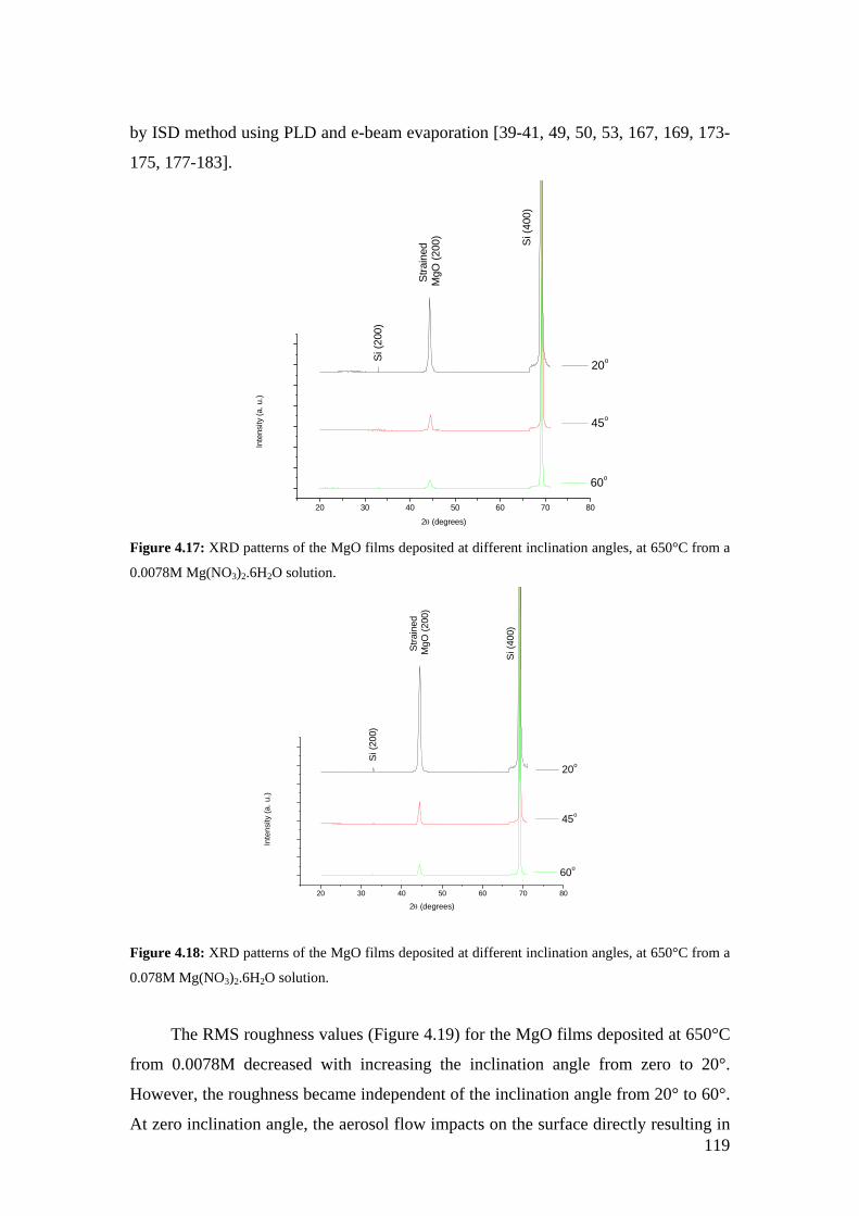
119
by ISD method using PLD and e-beam evaporation [39-41, 49, 50, 53, 167, 169, 173-
175, 177-183].
20 30 40 50 60 70 80
60o
20o
45o
Si (2
00)
Stra
ined
M
gO (2
00) Si (4
00)
Inte
nsity
(a. u
.)
2θ (degrees) Figure 4.17: XRD patterns of the MgO films deposited at different inclination angles, at 650°C from a
0.0078M Mg(NO3)2.6H2O solution.
20 30 40 50 60 70 80
60o
20o
45o
Stra
ined
M
gO (2
00)
Si (
200)
Si (4
00)
Inte
nsity
(a. u
.)
2θ (degrees)
Figure 4.18: XRD patterns of the MgO films deposited at different inclination angles, at 650°C from a
0.078M Mg(NO3)2.6H2O solution.
The RMS roughness values (Figure 4.19) for the MgO films deposited at 650°C
from 0.0078M decreased with increasing the inclination angle from zero to 20°.
However, the roughness became independent of the inclination angle from 20° to 60°.
At zero inclination angle, the aerosol flow impacts on the surface directly resulting in

120
rough films compared to that with substrate being inclined, where the probability of
direct impact is less, resulting in smoother films. When using 0.078M solution (Figure
4.19), however, the roughness values are almost independent of the inclination angles.
This disagrees with findings of Pavlopoulos [147], for the films deposited from
0.078M at 650°C, who found that the RMS values decreased by increasing the
inclination angle from zero to 10° and to 25° but they increased at 45°. The
corresponding roughness values were 34, 12, 8 and 54 nm, respectively. He attributed
the high roughness value at 45° to the formation of overgrown particles on the film
surface. However, the findings of this work agrees with the findings of Ratcheva and
Nanobva [241]. They found that in the case of In2O3:Te films prepared by spraying on
Si substrates, no influence of the spraying angle on the grain growth rate and grain
size was observed for two spraying angles, namely, 30° and 90°, and hence no
influence on the roughness. Rachel E. Koritala et al [185] found for the case of
biaxially textured MgO films deposited by ISD using e-beam evaporation on
Hastelloy C substrates that high roughness values was obtained at low and high
inclination angles and the lowest roughness values were obtained for inclination
angles of 20°-55° where the roughness was not affected by the inclination angle in
this range. In the present work, the roughness dependence (between 0.0078M and
0.078M) on the inclination angle can be attributed to the large difference in the used
concentrations. At 0.0078M, the concentration was low enough that a small change in
the inclination angle affects the aerosol delivery to the substrate leading to a
roughness variation between 0° and 20° which is not the case when using 0.078M.
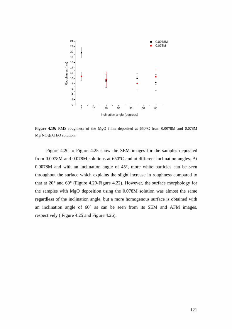
121
0 10 20 30 40 50 600
2
4
6
8
10
12
14
16
18
20
22
24 0.0078M 0.078M
Rou
ghne
ss (n
m)
Inclination angle (degrees)
Figure 4.19: RMS roughness of the MgO films deposited at 650°C from 0.0078M and 0.078M
Mg(NO3)2.6H2O solution.
Figure 4.20 to Figure 4.25 show the SEM images for the samples deposited
from 0.0078M and 0.078M solutions at 650°C and at different inclination angles. At
0.0078M and with an inclination angle of 45°, more white particles can be seen
throughout the surface which explains the slight increase in roughness compared to
that at 20° and 60° (Figure 4.20-Figure 4.22). However, the surface morphology for
the samples with MgO deposition using the 0.078M solution was almost the same
regardless of the inclination angle, but a more homogenous surface is obtained with
an inclination angle of 60° as can be seen from its SEM and AFM images,
respectively ( Figure 4.25 and Figure 4.26).
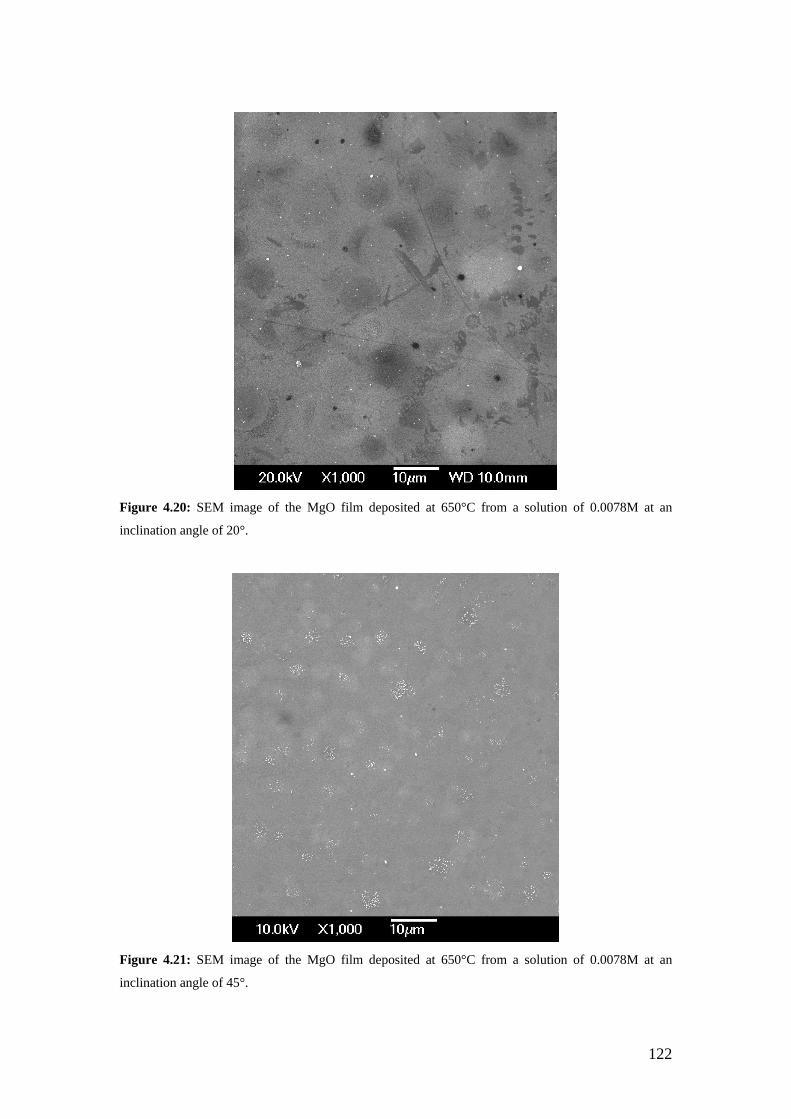
122
Figure 4.20: SEM image of the MgO film deposited at 650°C from a solution of 0.0078M at an
inclination angle of 20°.
Figure 4.21: SEM image of the MgO film deposited at 650°C from a solution of 0.0078M at an
inclination angle of 45°.

123
Figure 4.22: SEM image of the MgO film deposited at 650°C from a solution of 0.0078M at an
inclination angle of 60°.
Figure 4.23: SEM image of the MgO film deposited at 650°C from a solution of 0.078M at an
inclination angle of 20°.

124
Figure 4.24: SEM image of the MgO film deposited at 650°C from a solution of 0.078M at an
inclination angle of 45°.
Figure 4.25: SEM image of the MgO film deposited at 650°C from a solution of 0.078M at an
inclination angle of 60°.
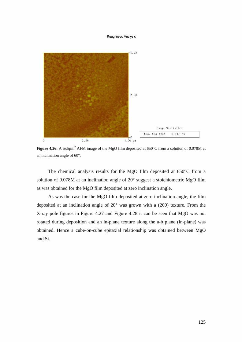
125
Figure 4.26: A 5x5µm2 AFM image of the MgO film deposited at 650°C from a solution of 0.078M at
an inclination angle of 60°.
The chemical analysis results for the MgO film deposited at 650°C from a
solution of 0.078M at an inclination angle of 20° suggest a stoichiometric MgO film
as was obtained for the MgO film deposited at zero inclination angle.
As was the case for the MgO film deposited at zero inclination angle, the film
deposited at an inclination angle of 20° was grown with a (200) texture. From the
X-ray pole figures in Figure 4.27 and Figure 4.28 it can be seen that MgO was not
rotated during deposition and an in-plane texture along the a-b plane (in-plane) was
obtained. Hence a cube-on-cube epitaxial relationship was obtained between MgO
and Si.
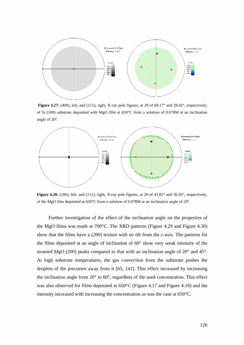
126
Figure 4.27: (400), left, and (111), right, X-ray pole figures, at 2θ of 69.17° and 28.42°, respectively,
of Si (100) substrate deposited with MgO film at 650°C from a solution of 0.078M at an inclination
angle of 20°.
Figure 4.28: (200), left, and (111), right, X-ray pole figures, at 2θ of 43.82° and 36.93°, respectively,
of the MgO film deposited at 650°C from a solution of 0.078M at an inclination angle of 20°.
Further investigation of the effect of the inclination angle on the properties of
the MgO films was made at 700°C. The XRD patterns (Figure 4.29 and Figure 4.30)
show that the films have a (200) texture with no tilt from the c-axis. The patterns for
the films deposited at an angle of inclination of 60° show very weak intensity of the
strained MgO (200) peaks compared to that with an inclination angle of 20° and 45°.
At high substrate temperatures, the gas convection from the substrate pushes the
droplets of the precursor away from it [65, 141]. This effect increased by increasing
the inclination angle from 20° to 60°, regardless of the used concentration. This effect
was also observed for films deposited at 650°C (Figure 4.17 and Figure 4.18) and the
intensity increased with increasing the concentration as was the case at 650°C.

127
20 30 40 50 60 70
20o
45o
60o
Stra
ined
M
gO (2
00)
Si (2
00)
Si (4
00)
Inte
nsity
(a. u
.)
2θ (degrees) Figure 4.29: XRD patterns of the MgO films deposited at different inclination angles, at 700°C from a
0.0078M Mg(NO3)2.6H2O solution.
20 30 40 50 60 70 80
60o
45o
20o
Stria
ned
MgO
(200
)
Si (
200)
Si (4
00)
Inte
nsity
(a. u
.)
2θ (degrees) Figure 4.30: XRD patterns of the MgO films deposited at different inclination angles, at 700°C from a
0.078M Mg(NO3)2.6H2O solution.
The RMS values (Figure 4.31) show that the roughness, at 0.0078M and
0.078M, decreased by increasing the inclination angle from zero to 60°. Hence, in
spray pyrolysis the ISD affects the crystallinity and roughness of the deposited MgO
films. It can also be seen that the roughness values of the MgO films deposited at
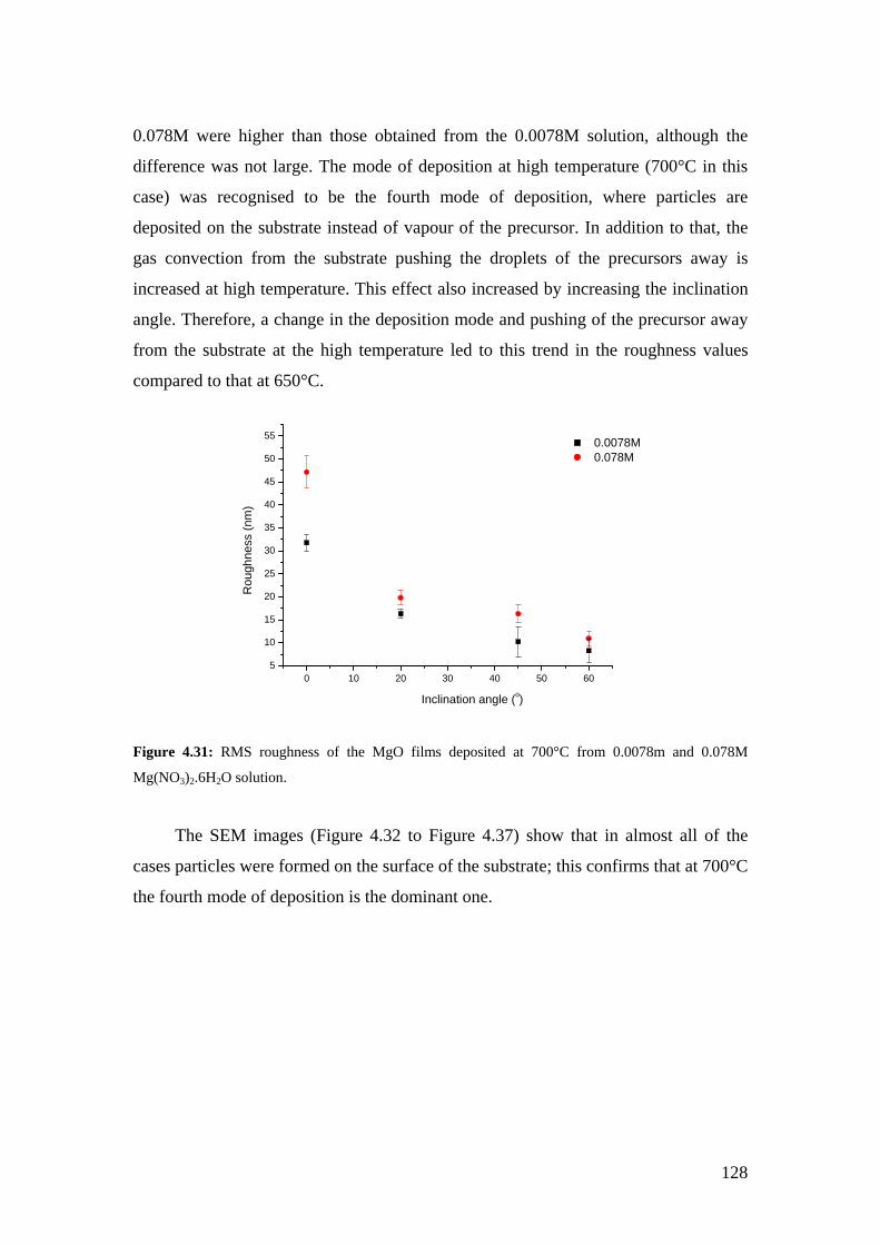
128
0.078M were higher than those obtained from the 0.0078M solution, although the
difference was not large. The mode of deposition at high temperature (700°C in this
case) was recognised to be the fourth mode of deposition, where particles are
deposited on the substrate instead of vapour of the precursor. In addition to that, the
gas convection from the substrate pushing the droplets of the precursors away is
increased at high temperature. This effect also increased by increasing the inclination
angle. Therefore, a change in the deposition mode and pushing of the precursor away
from the substrate at the high temperature led to this trend in the roughness values
compared to that at 650°C.
0 10 20 30 40 50 605
10
15
20
25
30
35
40
45
50
55 0.0078M 0.078M
Rou
ghne
ss (n
m)
Inclination angle (o)
Figure 4.31: RMS roughness of the MgO films deposited at 700°C from 0.0078m and 0.078M
Mg(NO3)2.6H2O solution.
The SEM images (Figure 4.32 to Figure 4.37) show that in almost all of the
cases particles were formed on the surface of the substrate; this confirms that at 700°C
the fourth mode of deposition is the dominant one.
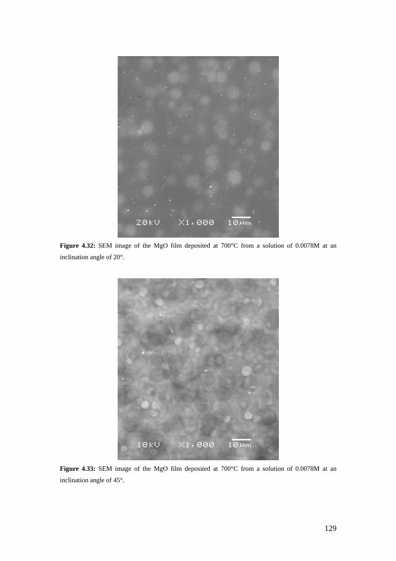
129
Figure 4.32: SEM image of the MgO film deposited at 700°C from a solution of 0.0078M at an
inclination angle of 20°.
Figure 4.33: SEM image of the MgO film deposited at 700°C from a solution of 0.0078M at an
inclination angle of 45°.

130
Figure 4.34: SEM image of the MgO film deposited at 700°C from a solution of 0.0078M at an
inclination angle of 60°.
Figure 4.35: SEM image of the MgO film deposited at 700°C from a solution of 0.078M at an
inclination angle of 20°.

131
Figure 4.36: SEM image of the MgO film deposited at 700°C from a solution of 0.078M at an
inclination angle of 45°.
Figure 4.37: SEM image of the MgO film deposited at 700°C from a solution of 0.078M at an
inclination angle of 60°.

132
Irrespective of the inclination angle and the used concentration, the deposited
MgO films have almost 1:1 ratio of Mg:O as suggested from the EDX tests. Also the
films have out-of-plane and in-plane texture. As an example, the X-ray pole figure for
the MgO film deposited at 700°C from a solution of 0.078M at an inclination angle of
20° is shown in Figure 4.39 together with the X-ray pole figure of the Si substrate
which is shown in Figure 4.38. The MgO film has a cube-on-cube texture relative to
the Si substrate, where no rotation of the MgO film was noticed relative to the Si
substrate to reduce the lattice mismatch.
Figure 4.38: (400), left, and (111), right, X-ray pole figures, at 2θ of 69.17° and 28.42°, respectively,
of Si (100) substrate deposited with MgO film at 700°C from a solution of 0.078M at an inclination
angle of 20°.
Figure 4.39: (200), left, and (111), right, X-ray pole figures, at 2θ of 43.96° and 36.93°, respectively of
the MgO film deposited at 700°C from a solution of 0.078M at an inclination angle of 20°.
It is known that ISD deposition is applied, either by PLD or e-beam, to grow
MgO thin films to improve the in plane texture for YBCO deposition. However, from
Figure 4.17, Figure 4.18, Figure 4.29, and Figure 4.30, it can be seen that the MgO
has only a (200) texture. This means that the ISD deposition by spray pyrolysis is not
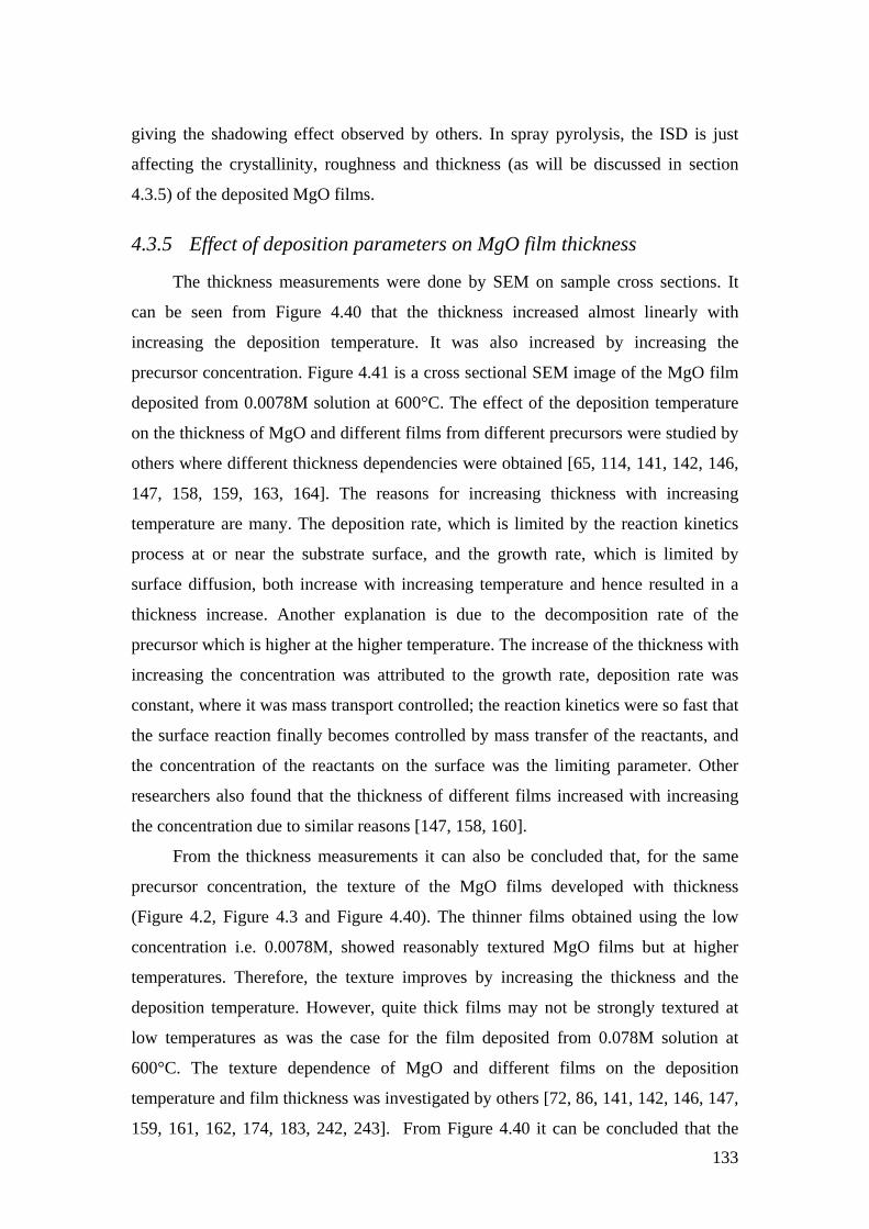
133
giving the shadowing effect observed by others. In spray pyrolysis, the ISD is just
affecting the crystallinity, roughness and thickness (as will be discussed in section
4.3.5) of the deposited MgO films.
4.3.5 Effect of deposition parameters on MgO film thickness
The thickness measurements were done by SEM on sample cross sections. It
can be seen from Figure 4.40 that the thickness increased almost linearly with
increasing the deposition temperature. It was also increased by increasing the
precursor concentration. Figure 4.41 is a cross sectional SEM image of the MgO film
deposited from 0.0078M solution at 600°C. The effect of the deposition temperature
on the thickness of MgO and different films from different precursors were studied by
others where different thickness dependencies were obtained [65, 114, 141, 142, 146,
147, 158, 159, 163, 164]. The reasons for increasing thickness with increasing
temperature are many. The deposition rate, which is limited by the reaction kinetics
process at or near the substrate surface, and the growth rate, which is limited by
surface diffusion, both increase with increasing temperature and hence resulted in a
thickness increase. Another explanation is due to the decomposition rate of the
precursor which is higher at the higher temperature. The increase of the thickness with
increasing the concentration was attributed to the growth rate, deposition rate was
constant, where it was mass transport controlled; the reaction kinetics were so fast that
the surface reaction finally becomes controlled by mass transfer of the reactants, and
the concentration of the reactants on the surface was the limiting parameter. Other
researchers also found that the thickness of different films increased with increasing
the concentration due to similar reasons [147, 158, 160].
From the thickness measurements it can also be concluded that, for the same
precursor concentration, the texture of the MgO films developed with thickness
(Figure 4.2, Figure 4.3 and Figure 4.40). The thinner films obtained using the low
concentration i.e. 0.0078M, showed reasonably textured MgO films but at higher
temperatures. Therefore, the texture improves by increasing the thickness and the
deposition temperature. However, quite thick films may not be strongly textured at
low temperatures as was the case for the film deposited from 0.078M solution at
600°C. The texture dependence of MgO and different films on the deposition
temperature and film thickness was investigated by others [72, 86, 141, 142, 146, 147,
159, 161, 162, 174, 183, 242, 243]. From Figure 4.40 it can be concluded that the

134
deposition rate depends on the deposition temperature and concentration. It ranged
from 4.75Å/sec (114Å/240sec) for the film deposited from 0.0078M solution at
600°C to 33Å/sec for the film deposited from 0.078M solution at 700°C. The
deposition rate for the film deposited from 0.078M solution at 650°C with zero
inclination angle was about 30Å/sec.
600 650 7000
100
200
300
400
500
600
700
800
900
1000 0.078M 0.0078M
Film
thic
knes
s (n
m)
Deposition temperature (OC)
Figure 4.40: Effect of deposition temperature and precursor concentration on MgO film thicknesses
deposited with zero inclination angle.
Figure 4.41: A cross sectional SEM image for MgO film deposited at 600°C from 0.0078M solution.

135
The effect of inclination angle on MgO film thicknesses was also studied. A
cross sectional SEM image for the MgO film deposited at 650°C from 0.078M
solution with an inclination angle of 45° is shown in Figure 4.42. Figure 4.43 shows
that the film thickness, at 650°C, decreased with increasing the inclination angle
irrespective of the used concentration. The higher the concentration and the lower the
inclination angle resulted in thicker (Figure 4.43) and rougher (Figure 4.19) MgO
films and the stronger the MgO (200) peaks i.e. better texture (Figure 4.17 and Figure
4.18). Similar thicknesses and observations were seen by Pavlopoulos D. [147] for the
films deposited from 0.078M at 650°C who found that film thicknesses decreased
almost linearly by increasing the inclination angle from 0° to 45°. The film prepared
with no inclination angle was around 750nm while the thinnest film around 200nm
was obtained when the inclination angle was set to 450 .Other researchers (using
e-beam evaporation to deposit MgO films) found that the texture evolved faster and
the films were thinner and rougher, due to the formation of voids and loose structure,
at high inclination angles compared to that at lower inclination angles. They also
found that the texture improved with thickness and with increasing the inclination
angle [39, 41, 50, 169, 174, 175, 177, 180, 182, 183]. Rachel E. Koritala et al [185]
found that, for MgO films deposited by e-beam on Hastelloy C276, the roughness
increased with increasing thickness. High roughness values were also obtained at low
and high inclination angles and the lowest roughness values were obtained for
inclination angles of 20°-55° where the roughness was not affected by the inclination
angle in this range. Develos et al [165] and Shigetoshi Ohshima et al [166] deposited
CeO2 films on Al2O3 films by PLD. They found that the surface roughness increased
with increasing the film thickness.
Figure 4.44 shows the effect of inclination angle and precursor concentration
on MgO film thicknesses at 700°C where it shows similar behaviour to those
deposited at 650°C. Figure 4.45 is a cross sectional image for MgO film deposited at
700°C from 0.078M solution with an inclination angle of 20°.

136
Figure 4.42: A cross sectional SEM image for MgO film deposited at 650°C from 0.078M solution
with an inclination angle of 45°.
0 10 20 30 40 50 60 700
100
200
300
400
500
600
700
800
900
1000 0.078M 0.0078M
Film
thic
knes
s (n
m)
Inclination angle (degrees)
Figure 4.43: Effect of inclination angle and precursor concentration on MgO film thicknesses (at a
deposition temperature of 650°C).

137
0 10 20 30 40 50 60 700
100
200
300
400
500
600
700
800
900
1000 0.078M 0.0078M
Film
thic
knes
s (n
m)
Inclination angle (degrees)
Figure 4.44: effect of inclination angle and precursor concentration on MgO film thicknesses (at a
deposition temperature of 700°C).
Figure 4.45: A cross sectional image for MgO film deposited at 700°C from 0.078M solution with an
inclination angle of 20°.

138
4.4 MgO deposition by pulsed laser deposition on Si (100) substrates
To evaluate the quality of MgO films deposited by spray pyrolysis, PLD was
used to deposit MgO films on the Si (100) substrates from MgO targets (99.95%
purity bought from THEVA). An excimer laser with a wavelength of 248nm was
utilised for the deposition. The MgO deposition parameters were:
The deposition temperature: 750°C.
Substrate target distance: 47mm.
Deposition pressure: 0.13mbar (~ 0.1 torr) O2.
Energy fluence: 3.0-3.45 J/cm2 (the energy of the beam was measured inside
the deposition chamber prior to each deposition and the target was ground to a
smooth finish before each deposition).
Number of pulses 4000.
Pulse frequency: 4Hz
Heating and cooling rates: 20°C/min and 4°C/min, respectively.
The Si substrates were cleaned in acetone and ethanol then loaded in the
deposition chamber; evacuation of the chamber was obtained by pumping down to
5x10⁻⁶ mbar (3.75x10⁻⁶ torr), the target was then cleaned and conditioned with a 1000
laser pulses under vacuum with a shutter being positioned over the substrate. After
heating to 750°C, the substrates were first deposited with MgO by 100 pulses under
high vacuum to minimise the formation of silicon oxides; then 0.13mbar of oxygen
was introduced. The deposition under high vacuum was made because the
introduction of O2 just before the deposition yields amorphous MgO layers [186].
This suggests that O2 gas introduced before the deposition of MgO films forms an
oxide layer on the substrate, which leads to the degradation of the crystallinity of the
MgO films [186]. For comparison another MgO deposition was completely made
under 0.13mbar oxygen pressure. Cooling of the substrate was under 0.7 bar O2 which
was introduced in the chamber over 8 minutes while maintaining the substrate
temperature.
Figure 4.46 shows the XRD patterns for the MgO films deposited by PLD on Si
(100) substrates at different energy fluencies and compared to the MgO film deposited
by spray pyrolysis from 0.078M magnesium nitrate solution at 650°C with zero
inclination angle. It was clear that the intensity of MgO increased by increasing the
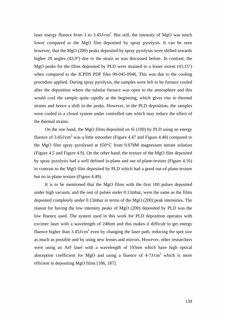
139
laser energy fluence from 3 to 3.45J/cm2. But still, the intensity of MgO was much
lower compared to the MgO film deposited by spray pyrolysis. It can be seen
however, that the MgO (200) peaks deposited by spray pyrolysis were shifted towards
higher 2θ angles (43.9°) due to the strain as was discussed before. In contrast, the
MgO peaks for the films deposited by PLD were strained to a lesser extent (43.15°)
when compared to the JCPDS PDF files 00-045-0946. This was due to the cooling
procedure applied. During spray pyrolysis, the samples were left to be furnace cooled
after the deposition where the tubular furnace was open to the atmosphere and this
would cool the sample quite rapidly at the beginning, which gives rise to thermal
strains and hence a shift in the peaks. However, in the PLD deposition, the samples
were cooled in a closed system under controlled rate which may reduce the effect of
the thermal strains.
On the one hand, the MgO films deposited on Si (100) by PLD using an energy
fluence of 3.45J/cm2 was a little smoother (Figure 4.47 and Figure 4.48) compared to
the MgO film spray pyrolysed at 650°C from 0.078M magnesium nitrate solution
(Figure 4.5 and Figure 4.9). On the other hand, the texture of the MgO film deposited
by spray pyrolysis had a well defined in-plane and out of-plane-texture (Figure 4.16)
in contrast to the MgO film deposited by PLD which had a good out-of-plane texture
but no in-plane texture (Figure 4.49).
It is to be mentioned that the MgO films with the first 100 pulses deposited
under high vacuum, and the rest of pulses under 0.13mbar, were the same as the films
deposited completely under 0.13mbar in terms of the MgO (200) peak intensities. The
reason for having the low intensity peaks of MgO (200) deposited by PLD was the
low fluence used. The system used in this work for PLD deposition operates with
excimer laser with a wavelength of 248nm and this makes it difficult to get energy
fluence higher than 3.45J/cm2 even by changing the laser path, reducing the spot size
as much as possible and by using new lenses and mirrors. However, other researchers
were using an ArF laser with a wavelength of 193nm which have high optical
absorption coefficient for MgO and using a fluence of 4-7J/cm2 which is more
efficient in depositing MgO films [186, 187].

140
20 30 40 50 60 70 80
0.078M 650OC
MgO
(200
)
Si (2
00)
Si (4
00)
3.45J/cm2
3J/cm2
Inte
nsity
(a. u
.)
2θ (degrees)
Figure 4.46: XRD patterns for MgO deposition on Si (100) substrate by PLD at different fluencies and
compared to MgO deposition by spray pyrolysis using 0.078M of magnesium nitrate at 650°C with
zero inclination angle.
Figure 4.47: SEM image for MgO film deposited by PLD on Si (100) at an energy fluence of
3.45J/cm2.

141
Figure 4.48: A 5x5µm2 AFM image for MgO film deposited by PLD on Si (100) at an energy fluence
of 3.45J/cm2.
Figure 4.49: (200) X-ray pole figure at 2θ=43.10° of the MgO film deposited by PLD on Si (100) at an
energy fluence of 3.45J/cm2.
4.5 Optimisation of YBCO deposition parameters
To evaluate the performance of the spray pyrolysed MgO films as a buffer,
YBCO films were deposited by PLD on top of them. This is a well established route
to high quality films [244, 245], although spray pyrolysis of the YBCO layer should
also be a possibility in the future [23, 24, 87, 93, 94].
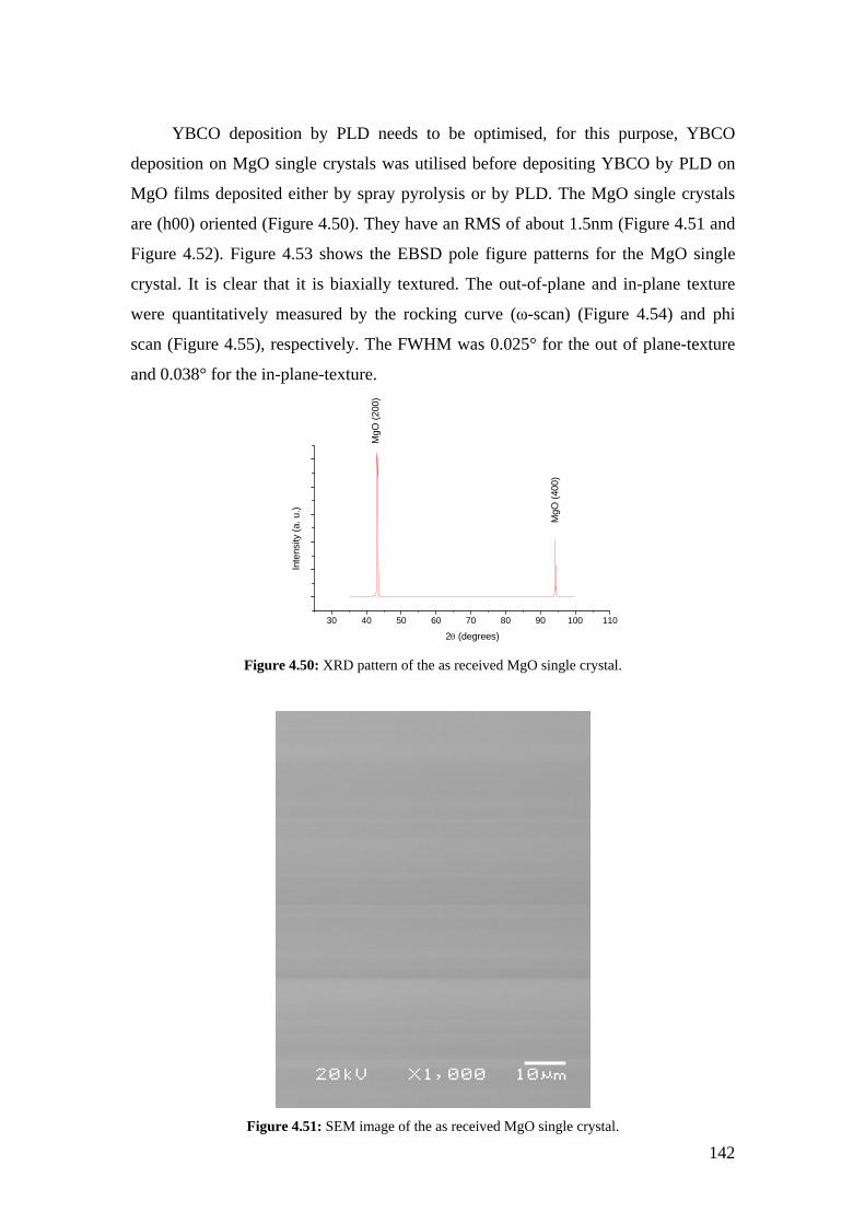
142
YBCO deposition by PLD needs to be optimised, for this purpose, YBCO
deposition on MgO single crystals was utilised before depositing YBCO by PLD on
MgO films deposited either by spray pyrolysis or by PLD. The MgO single crystals
are (h00) oriented (Figure 4.50). They have an RMS of about 1.5nm (Figure 4.51 and
Figure 4.52). Figure 4.53 shows the EBSD pole figure patterns for the MgO single
crystal. It is clear that it is biaxially textured. The out-of-plane and in-plane texture
were quantitatively measured by the rocking curve (ω-scan) (Figure 4.54) and phi
scan (Figure 4.55), respectively. The FWHM was 0.025° for the out of plane-texture
and 0.038° for the in-plane-texture.
30 40 50 60 70 80 90 100 110
Inte
nsity
(a. u
.)
2θ (degrees)
MgO
(200
)
MgO
(400
)
Figure 4.50: XRD pattern of the as received MgO single crystal.
Figure 4.51: SEM image of the as received MgO single crystal.
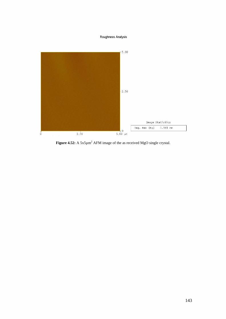
143
Figure 4.52: A 5x5µm2 AFM image of the as received MgO single crystal.

144
Figure 4.53: EBSD pole figure patterns for MgO single crystal showing the MgO {100}, {110} and
{111} planes.
21.35 21.40 21.45 21.50 21.55 21.60
Inte
nsity
(a. u
.)
ω scan (degrees)
Figure 4.54: X-ray diffraction ω−scan for MgO (200) with a FWHM of 0.025ο.

145
-200 -150 -100 -50 0 50 100
FWHM 0.029
-8 7 . 1 5 - 8 7 .1 0 -8 7 . 0 5 -8 7 . 0 0 - 8 6 .9 5 -8 6 .9 0 -8 6 .8 5
0
1 0 0 0 0
2 0 0 0 0
3 0 0 0 0
4 0 0 0 0
5 0 0 0 0
Inte
ns
ity
(a.
u.)
φ s c a n ( d e g r e e s )
FWHM 0.03
92.75 92.80 92.85 92.90 92.9 5 93.00
0
10000
20000
30000
40000
Inte
nsi
ty (
a. u
.)
φ (degrees)
FWHM 0.059
-177.05 -177.00 -176.95 -176.90 -176.85 -176.80
0
5000
10000
15000
20000
25000
30000
Inte
nsity
(a. u
.)
φ (degrees)
FWHM 0.035
2.74 2.76 2.78 2.80 2.82 2.84 2.86 2.88 2.90 2.92-5000
0
5000
10000
15000
20000
25000
30000
35000
40000
Inten
sity (a
. u.)
φ (degrees)
Inte
nsity
(a. u
.)
φ scan (degrees)
Figure 4.55: X-ray diffraction Φ−scan for MgO (220) with a FWHM of about 0.038ο.
4.5.1 YBCO deposition by pulsed laser deposition on MgO single crystals
YBCO was deposited on MgO single crystals using different fluencies (J/cm2)
and different number of pulses (i.e. different thicknesses) under 450 mtorr O2 which
was utilized during deposition. The deposition temperature was 780°C, the heating
and cooling rates were 20°C/min and 10°C/min, respectively. The target-substrate
distance was fixed at 56mm and the used pulse frequency was 4Hz.
Figure 4.56 shows the XRD patterns for YBCO films deposited on MgO single
crystals at 2 and 2.75J/cm2 and using 2000, 5000 and 10000 pulses. The MgO and
YBCO peaks were indexed according to the JCPDS PDF files 00-045-0946 and
00-038-1433, respectively. YBCO has an orthorhombic structure with lattice
parameters of a= 3.8185Å, b=3.8856Å and c=11.6804Å according to the JCPDS PDF
file 00-038-1433. The (001), (002), (003), (004), (005), (006), (007), (103), (113),
(115), (116) are at 2θs of 7.55°, 15.17°, 22.83°, 30.62°, 38.51°, 46.63°, 54.99°,
32.89°, 40.38°, 51.49°, 58.21°, respectively. The thermal expansion coefficient of
YBCO is 13.0-13.4x10⁻⁶/K [95, 246]. It can be seen that all of the YBCO films are 00l
oriented with the (006) peak being the strongest. A log scale pattern for YBCO films
(Figure 4.57) shows the formation of a weak YBCO (103) peak which was believed to
be a nucleation problem during YBCO deposition.

146
0 10 20 30 40 50 60
YBC
O (0
04)
2000 pulses 2J/cm2
2000 pulses 2.75J/cm2
5000 pulses 2J/cm2
10000 pulses 2J/cm2
YBC
O (0
07)YB
CO
(006
)
MgO
(200
)
YBC
O (0
05)
YBC
O (0
03)
YBC
O (0
02)
YBC
O (0
01)
Inte
nsity
(a. u
.)
2θ (degrees)
Figure 4.56: XRD patterns for YBCO films deposited on MgO single crystal using different number of
pulses and different fluencies.
0 10 20 30 40 50 60
YBC
O (1
03)
2000 pulses 2J/cm2
2000 pulses 2.75J/cm2
5000 pulses 2J/cm2
10000 pulses 2J/cm2
YBC
O (0
07)YB
CO
(006
)
MgO
(200
)
YBC
O (0
05)
YBC
O (0
04)
YBC
O (0
03)
YBC
O (0
02)
YBC
O (0
01)
Inte
nsity
(a. u
.)
2θ (degrees)
Figure 4.57: XRD patterns in log scale for YBCO films deposited on MgO single crystal using
different number of pulses and different fluencies.
The films deposited with 2000 pulses show that the intensity of YBCO (006)
decreased with increasing the fluence from 2 to 2.75J/cm2. At high fluence, more

147
material should be ablated from the target; this may also be combined by the
formation of molten droplets or particulates which makes the ablation process less
efficient and affects the film quality [245, 247-249] where it may affect the nucleation
and growth process, hence disturbing the texture of the YBCO film. The SEM and
AFM images (Figure 4.58-Figure 4.61) show that the films are porous and that the
roughness increased by increasing the fluence from 2.0-2.75 J/cm2. Such porous films
were noticed by others where it was attributed to the formation of Y2O3 precipitates or
yttrium rich secondary phase i.e. BaY2O4 [208, 209, 212].
Figure 4.58: SEM image for a 2000 pulses YBCO film deposited on MgO single crystal using a
fluence of 2 J/cm2.
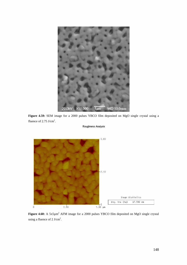
148
Figure 4.59: SEM image for a 2000 pulses YBCO film deposited on MgO single crystal using a
fluence of 2.75 J/cm2.
Figure 4.60: A 5x5µm2 AFM image for a 2000 pulses YBCO film deposited on MgO single crystal
using a fluence of 2 J/cm2.

149
Figure 4.61: A 5x5µm2 AFM image for a 2000 pulses YBCO film deposited on MgO single crystal
using a fluence of 2.75 J/cm2.
Both of the YBCO films deposited using 2000 pulses have a well defined
in-plane and out-of-plane texture as can be seen from the EBSD pole figure patterns
in Figure 4.62 and Figure 4.63. However, large grain misorientation in the film
deposited using 2.75 J/cm2 (Figure 4.65) was worse compared to the film deposited
using 2 J/cm2 (Figure 4.64). Large grain misorientation is known to affect the
superconducting properties [30, 197, 198, 205-207].
Figure 4.62: EBSD pole figure patterns for a 2000 pulses YBCO film deposited on MgO single crystal
using a fluence of 2 J/cm2 showing the YBCO {006} and {103} planes.

150
Figure 4.63: EBSD pole figure patterns for a 2000 pulses YBCO film deposited on MgO single crystal
using a fluence of 2.75 J/cm2 showing the YBCO {006} and {103} planes.
Figure 4.64: EBSD histogram for a 2000 pulses YBCO film deposited on MgO single crystal using a
fluence of 2J/cm2 showing misorientation angles.

151
Figure 4.65: EBSD histogram for a 2000 pulses YBCO film deposited on MgO single crystal using a
fluence of 2.75J/cm2 showing misorientation angles.
The AC susceptibility test (Figure 4.76) showed a broad superconducting
transition temperature for the film deposited with 2.75 J/cm2 with a Tc onset of 86.9K
whereas a sharp transition temperature with a Tc onset of 87.4K was obtained for the
film deposited at 2 J/cm2. This confirms that the optimum fluence for YBCO
deposition in the used system during this work is 2J/cm2.
By increasing the number of pulses to 5000 and 10,000 while keeping the
fluence at 2 J/cm2, the intensity of YBCO (006) was the same for both films (Figure
4.57). The SEM and AFM images (Figure 4.66-Figure 4.69) show that the films are
less porous compared to films with 2000 pulses (Figure 4.58). Figure 4.70 is a cross
sectional SEM image for an YBCO film deposited with 10,000 pulses showing a film
thickness of 1.922µm which gives a deposition rate of (19220/10000) = 1.922Å/pulse.
Therefore, the film deposited with a 5000 pulses should have a thickness of 0.96µm
where the measured thickness was about 1.01µm. The film roughness increased by
increasing the number of pulses from 5000 to 10,000 (Figure 4.68 and Figure 4.69),
although both films had a well defined in-plane and out-of-plane texture (Figure 4.71
and Figure 4.72). Both films also had sharp transition temperatures of 91.9K for the
5000 pulses film and 92K for the 10,000 pulses film (Figure 4.76). The out-of-plane
and in-plane texture for the 5000 pulses film were measured quantitatively using the
rocking curve and phi scans, respectively. The out-of-plane texture was found to have

152
a FWHM of 1.03° (Figure 4.73) and that for the in-plane texture of 1.8° (Figure 4.74).
The film was also found to consist mainly of low angle grains (Figure 4.75).
From the above, and as the critical current density decreases with increasing
YBCO thickness [213], it can be concluded that the optimum conditions for YBCO
deposition, which gives highest Tc, smoothest film, low angle grains and high quality
in-plane and out-of plane texture were to use 5000 pulses and a fluence of 2 J/cm2.
Figure 4.66: SEM image for a 5000 pulses YBCO film deposited on MgO single crystal using a
fluence of 2 J/cm2.

153
Figure 4.67: SEM image for a 10000 pulses YBCO film deposited on MgO single crystal using a
fluence of 2 J/cm2.
Figure 4.68: A 5x5µm2 AFM image for a 5000 pulses YBCO film deposited on MgO single crystal
using a fluence of 2 J/cm2.

154
Figure 4.69: A 5x5µm2 AFM image for a 10000 pulses YBCO film deposited on MgO single crystal
using a fluence of 2 J/cm2.
Figure 4.70: A cross sectional SEM image for a 10000 pulses YBCO film deposited on MgO single
crystal using a fluence of 2 J/cm2.

155
Figure 4.71: EBSD pole figure patterns for a 5000 pulses YBCO film deposited on MgO single crystal
using a fluence of 2 J/cm2 showing the YBCO {006} and {103} planes.
Figure 4.72: EBSD pole figure patterns for a 10000 pulses YBCO film deposited on MgO single
crystal using a fluence of 2 J/cm2 showing the YBCO {006} and {103} planes.

156
20 21 22 23 24 25 26 27
Inte
nsity
(a. u
.)
ω scan (degrees)
Figure 4.73: X-ray diffraction ω−scan for a 5000 pulses YBCO film deposited on MgO single crystal
using a fluence of 2J/cm2 showing a FWHM of 1.03ο.
-150 -100 -50 0 50 100 150 200
-92 -90 -88 -86 -84 -82
0
1000
2000
3000
4000
5000
6000
Inte
nsity
(a. u
.)
φ (degrees)
9 0 9 1 9 2 9 3 9 4 9 50
5 0 0
1 0 0 0
1 5 0 0
2 0 0 0
2 5 0 0
3 0 0 0
3 5 0 0
Inte
nsi
ty (
a.
u.)
φ (d eg ree s)
-2 0 2 4 6 8 10
0
1000
2000
3000
4000
5000
6000
Inte
nsity
(a.
u.)
φ (degrees)
FWHM1.79
269 270 271 272 273 274 275 276
0
1000
2000
3000
4000
5000
Inte
nsity
(a
. u.)
φ (degrees)
FWHM1.86
FWHM1.77FWHM
1.8
Inte
nsity
(a. u
.)
φ (degrees)
Figure 4.74: X-ray diffraction Φ−scan for a 5000 pulses YBCO film deposited on MgO single crystal
using a fluence of 2J/cm2 showing a FWHM of 1.8ο.

157
Figure 4.75: EBSD histogram for a 5000 pulses YBCO film deposited on MgO single crystal using a
fluence of 2J/cm2 showing misorientation angles.
20 40 60 80 100 120
2000 pulses 2J/cm2 87.4K 2000 pulses 2.75J/cm2 TC=86.9K 5000 pulses 2J/cm2 TC=91.9K 10000 pulses 2J/cm2 TC=92K
χ/ (a. u
.)
Temperature (K)
Figure 4.76: AC susceptibility test showing χ/ for YBCO films deposited on MgO single crystal at
different number of pulses and different fluencies.
4.6 YBCO deposition by pulsed laser deposition on Si (100)
substrates buffered with MgO
To evaluate the performance of the MgO films deposited by spray pyrolysis and
PLD, YBCO was deposited by PLD on top of them. This is a well established route to
high quality films [244, 245], although spray pyrolysis of the YBCO layer should also

158
be a possibility in the future [23, 24, 87, 93, 94]. The optimised parameters for YBCO
deposition were obtained by first depositing YBCO on MgO single crystal (section
4.5.1). The optimised and used YBCO deposition parameters were:
The deposition temperature: 780°C.
Substrate target distance: 56mm.
Deposition pressure: 450mtorr oxygen.
Energy fluence: 2J/cm2.
Number of pulses: 500 and 5000.
Pulse frequency: 4Hz
Heating rates: 20°C/min and the used cooling rate was 5°C/min, instead of
10°C/min to avoid film cracking due to thermal and lattice mismatch with
silicon.
Some researchers limited the deposition of YBCO films on Si substrates,
buffered with CeO2 and YSZ, to 40-50nm to minimise the effect of thermal stresses
which decrease the film’s critical temperature and current density [95, 250, 251].
Therefore, in this work YBCO deposition was first applied using 500 pulses.
However, no YBCO peaks were detected irrespective of the YBCO deposition
conditions. Others found that films with less than 50nm resulted in strained YBCO
films with distorted unit cells [252]. Therefore, YBCO deposition will be limited to
5000 pulses.
Figure 4.77 shows the XRD pattern for an YBCO film deposited on Si (100)
buffered with MgO spray pyrolysed at 650C using 0.078M solution of magnesium
nitrate at zero inclination angle. It is clear that the film has a strong texture along the
c-axis, however, a strong (103) peak was obtained as well (weak (103) peaks were
obtained when depositing YBCO on MgO single crystals as can be seen in Figure
4.57). This was not surprising because the MgO film deposited on Si was under
tension in-plane and under compression out-of-plane due to the thermal expansion
mismatch. Therefore, it was believed that the strained MgO layer disturbed the YBCO
deposition and led to this kind of partial texture. Therefore, the film had out-of-plane
texture but no in-plane texture (Figure 4.78). The surface roughness after YBCO
deposition (Figure 4.79 and Figure 4.80) was increased compared to the roughness of
the MgO buffer (Figure 4.5 and Figure 4.9) and the YBCO film had a broad
superconducting transition temperature (Figure 4.81). YBCO films deposited on MgO

159
spray pyrolysed from 0.078M at 650°C and 700°C with an inclination angle of 20°
resulted in polycrystalline YBCO films with no Tc. The YBCO film deposited on
MgO film, deposited on Si (100) by PLD using and energy fluence of 3.45J/cm2, was
polycrystalline as well with no Tc. This time it was attributed to the weak texture of
MgO film.
20 30 40 50 60 700
YBC
O(0
04)
YBC
O(0
07)
MgO
(200
)YB
CO
(006
)
Inte
nsity
(a. u
.)
2θ (degrees)
YBC
O(0
03)
YBC
O(0
05)
YBC
O (1
03)
Si (
200)
Si (
400)
Figure 4.77: XRD pattern for YBCO film deposited on Si (100) buffered with MgO spray pyrolysed at
650°C using 0.078M solution of magnesium nitrate at zero inclination angle.
Figure 4.78: EBSD pole figure pattern showing the {006} planes for YBCO film deposited on Si (100)
buffered with MgO spray pyrolysed at 650°C using 0.078M solution of magnesium nitrate at zero
inclination angle.
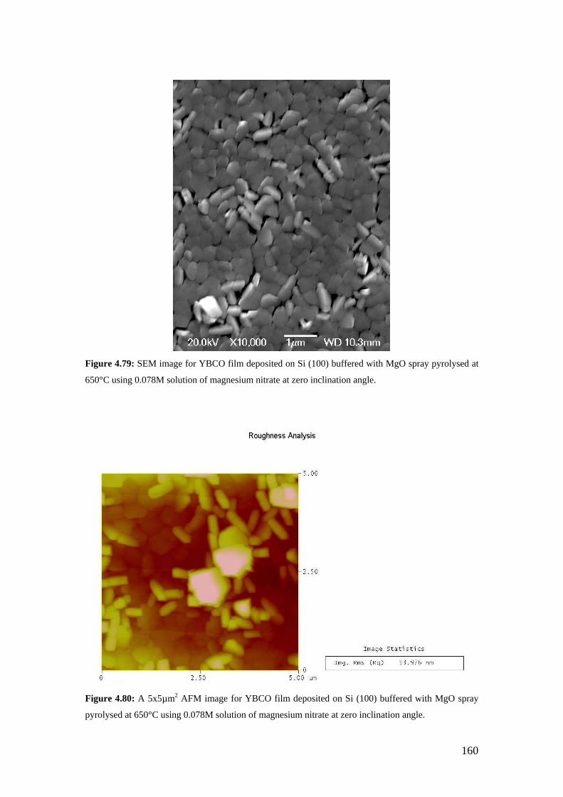
160
Figure 4.79: SEM image for YBCO film deposited on Si (100) buffered with MgO spray pyrolysed at
650°C using 0.078M solution of magnesium nitrate at zero inclination angle.
Figure 4.80: A 5x5µm2 AFM image for YBCO film deposited on Si (100) buffered with MgO spray
pyrolysed at 650°C using 0.078M solution of magnesium nitrate at zero inclination angle.

161
20 40 60 80 100 120
χ/ (a. u
.)
Temperature (K)
Figure 4.81: AC susceptibility test showing χ/ for YBCO film deposited on Si (100) buffered with
MgO spray pyrolysed at 650°C using 0.078M solution of magnesium nitrate at zero inclination angle.

162
5 Spray Pyrolysis of MgO on RABiTS NiW

163
5.1 Introduction
In this chapter the deposition of MgO thin films by spray pyrolysis on NiW
RABiTS will be introduced using mainly magnesium nitrate as a precursor. NiW tape
(100µm thick) was cut into 10mm x 10mm substrates. The samples were
polycrystalline; therefore, they were heat treated for recrystallisation. Some of them
were then mechanically polished down to a roughness of 2-5 nm, and then they were
cleaned in acetone, then ethanol for 10 minutes each in an ultrasonic bath, then dried
with Ar gas. In the spray pyrolysis deposition, a pulse time to interval time of 1:7 was
applied for 32 minutes; however, the precursor concentration was varied. The used Ar
flow rate was 10 l/min. In addition to that, MgO deposition was also applied on an
epitaxial oxide i.e. NiO (200) formed on top of the NiW tapes by oxidation.
As far as we know, no reports have been found for MgO deposition on metallic
substrates by spray pyrolysis. The aim of depositing MgO by spray pyrolysis is to
reduce the cost of production instead of using the relatively expensive methods for the
buffer layer deposition, such as electron beam evaporation [82] and pulse laser
deposition [80]. In section 4.5.1 YBCO was deposited on MgO single crystals to
demonstrate that MgO was a good substrate for YBCO deposition where a sharp
transition temperature was obtained with a Tc onset of about 91K. Therefore, a further
objective of the work was to grow MgO as the only buffer layer before YBCO
deposition in an attempt to make the process a cost-effective one by reducing the
usual multi-layer buffer architecture to a single layer.
5.2 NiW substrates
The chemical composition of the NiW substrates, as received from the supplier,
was checked by the EDX (using an accelerating voltage of 20 KV).
Table 5.1 shows that the chemical composition of the as received substrates was
about Ni-5at%W.

164
Table 5.1: Chemical composition of the as received NiW substrates.
Element
Chemical
composition, at%
(EDX, 20KV )
Ni K 94.78
W L 5.22
The surface roughness of the as received substrates, as shown from the AFM
image in Figure 5.1, shows that the roughness was about 50nm.
Figure 5.1: A 5x5µm2 AFM image of the as received NiW substrates.
Figure 5.2 shows the XRD pattern taken from the NiW substrate with the peaks
being indexed according to the JCPDS PDF file 00-004-0850 where the lattice
parameter is 3.5238Å (The 2θs for Ni (111), Ni (200), Ni (220), Ni (311) and Ni (400)
are 44.50°, 51.85°, 76.37°, 92.95° and 121.94°, respectively). From the XRD pattern
it is clear the substrates are polycrystalline with the Ni (220) being the strongest peak.
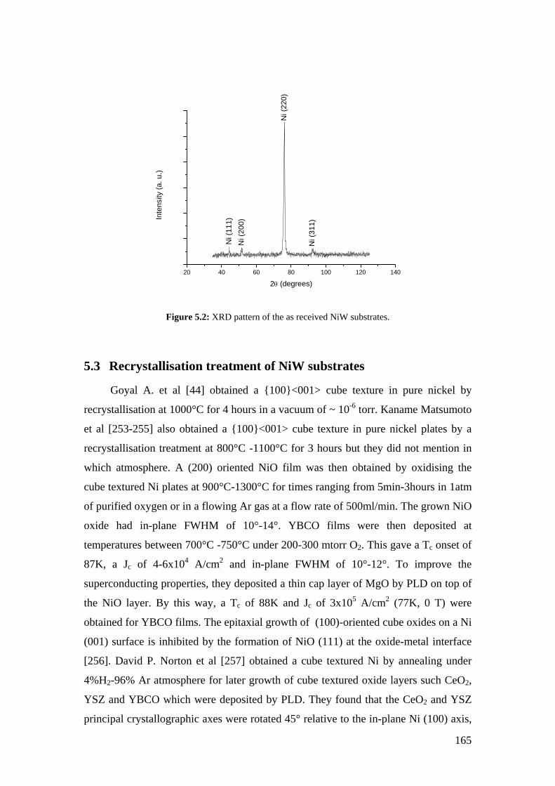
165
20 40 60 80 100 120 140
Ni (
311)
Ni (
200)
Ni (
111)
Ni (
220)
Inte
nsity
(a. u
.)
2θ (degrees)
Figure 5.2: XRD pattern of the as received NiW substrates.
5.3 Recrystallisation treatment of NiW substrates
Goyal A. et al [44] obtained a {100}<001> cube texture in pure nickel by
recrystallisation at 1000°C for 4 hours in a vacuum of ~ 10-6 torr. Kaname Matsumoto
et al [253-255] also obtained a {100}<001> cube texture in pure nickel plates by a
recrystallisation treatment at 800°C -1100°C for 3 hours but they did not mention in
which atmosphere. A (200) oriented NiO film was then obtained by oxidising the
cube textured Ni plates at 900°C-1300°C for times ranging from 5min-3hours in 1atm
of purified oxygen or in a flowing Ar gas at a flow rate of 500ml/min. The grown NiO
oxide had in-plane FWHM of 10°-14°. YBCO films were then deposited at
temperatures between 700°C -750°C under 200-300 mtorr O2. This gave a Tc onset of
87K, a Jc of 4-6x10⁴ A/cm2 and in-plane FWHM of 10°-12°. To improve the
superconducting properties, they deposited a thin cap layer of MgO by PLD on top of
the NiO layer. By this way, a Tc of 88K and Jc of 3x10⁵ A/cm2 (77K, 0 T) were
obtained for YBCO films. The epitaxial growth of (100)-oriented cube oxides on a Ni
(001) surface is inhibited by the formation of NiO (111) at the oxide-metal interface
[256]. David P. Norton et al [257] obtained a cube textured Ni by annealing under
4%H2-96% Ar atmosphere for later growth of cube textured oxide layers such CeO2,
YSZ and YBCO which were deposited by PLD. They found that the CeO2 and YSZ
principal crystallographic axes were rotated 45° relative to the in-plane Ni (100) axis,

166
whereas YBCO was rotated 45° with respect to YSZ, however, they produced several
films with Jc (77 K, H = 0) greater than 600,000 A/cm2. R.I. Chakalova et al [258]
deposited YBCO on biaxially textured Ni tapes using YSZ and CeO2 in different
combinations. To prevent the oxidation of the Ni substrate, 4% H2 in Ar was used. A
Tc of 80k-90K was obtained depending on the used buffer architecture. Y L Cheung et
al [259] deposited multilayer YBCO film insulated with STO on NiW RABiTS using
CeO2/YSZ/CeO2 buffer architecture. 4% H2 in Ar was introduced in the chamber
during heating to prevent oxidation of the substrate. The YBCO films separated with
STO were found to have a higher Tc and smaller transition width than YBCO films
separated using CeO2 and Y2O3 insulating layers. E Maher et al [260] succeeded in
depositing YBCO films on curved Ni tapes as a principle of multi-layer coil
fabrication. Y L Cheung et al [261] also succeeded in depositing YBCO films on
buffered curved NiW RABiTS by pulsed laser deposition to demonstrate the
feasibility of fabricating in-situ a multi-turn superconducting coil on a cylindrical
heated former. T. G. Woodcock et al [262, 263] grew biaxially textured NiO films on
biaxially textured Ni substrates by thermal oxidation at 1200°C for 1 hour in flowing
oxygen. The NiO films were (200) oriented, however, small NiO (111) peaks were
obtained as well. They found that up-quenching to the oxidation temperature and
down-quenching after holding for 1 hour gave rough surfaces compared to that when
the sample was ramped at 300°C/hour and furnace cooled after holding at the
oxidation temperature. This latter heating cycle gave smoother surfaces and therefore
more suitable for the deposition of subsequent functional layers. They also found that
the cube textured material appears to grow with a grain size very similar to that of the
substrate material, suggesting that an epitaxial growth mechanism may be in
operation. This may not be the case, as the observed orientation relationship would
result in a highly strained interface due to the large lattice misfit (18%) between Ni
and NiO. Khoi et al [256] grew (100) NiO on (100) Ni cylinders between
500°C-800°C, however, there was a 45° rotation of the NiO film relative to the
substrate i.e. (110) NiO // (100) Ni. They also found that the orientation of the oxide
layer changed with thickness.
The recrystallisation treatments in this work were carried out in a tube furnace
rated to 1200°C. The treatment was carried out at 1100°C for 3 hours under Ar-5%H2
atmosphere. The gas mixture was supplied from a compressed gas cylinder through
copper tubing. The gas flow was controlled and was set at 100ml/min for a furnace

167
volume of 1630ml. Before heating, the gas mixture was supplied to the furnace for
one hour which means that the furnace volume was replaced 3.7 times. The heating
was then carried out at a rate of 300C°/hr. After heating to the required temperature
and holding for the required time, the furnace was switched off to allow the samples
to be furnace cooled under the same atmosphere. Figure 5.3 shows the XRD pattern
for the sample after the recrystallisation treatment. It can be seen that the sample was
strongly (200) textured with no other peaks and was biaxially textured (Figure 5.4).
Figure 5.5 shows the SEM image of the sample after the recrystallisation treatment
where the grain boundaries were revealed due to the thermal etching effect. The
revealing of the grain boundaries at high temperatures was even seen during pulsed
laser disposition of YBCO on NiW RABiTS by Y L Cheung et al [259, 261]. The
thermal etching effect on Ni RABiTS was also seen by others [32, 264, 265]. The
roughness after the recrystallisation treatment was about 14nm as can be seen from
the AFM image in Figure 5.6.
20 40 60 80 100 120 140
Log scale
20 40 60 80 100 120 140
Kα2
Kα1
Ni (
400)Ni (
200)
Inte
nsity
(a.
u.)
2θ (degrees)
Kα2
Kα1
Ni (
400)
Ni (
200)
Inte
nsity
(a. u
.)
2θ (degrees)
Figure 5.3: XRD pattern of the as received NiW substrates after the recrystallisation treatment.

168
Figure 5.4: (200), left, and (111), right, X-ray pole figures, at 2θ of 51.6° and 44.5°, respectively, of
the as received NiW substrates after the recrystallisation treatment.
Figure 5.5: SEM image of the as received NiW substrate after the recrystallisation treatment.

169
Figure 5.6: A 5x5µm2 AFM image of the as received NiW substrates after the recrystallisation
treatment.
After the recrystallisation treatment, the substrates were mechanically polished
down to a roughness of 2-5nm (Figure 5.7 and Figure 5.8) and this had no effect on
the texture of the NiW substrate.
Figure 5.7: SEM image of the as received NiW substrates after the recrystallisation treatment and
mechanical polish.

170
Figure 5.8: A 5x5µm2 AFM image of the as received NiW substrates after the recrystallisation
treatment and mechanical polish.
5.4 MgO deposition on NiW RABiTS by spray pyrolysis using
magnesium nitrate precursor
After the recrystallisation treatment, MgO was deposited on NiW tapes by spray
pyrolysis using Mg(NO3)2.6H2O as a precursor. The deposition was carried out at
650°C using 0.078M-0.468M of the precursor on the polished and unpolished NiW
substrates. No MgO XRD peaks were detected, even when using the high solution
concentration, as can be seen from the XRD patterns in Figure 5.9 for the polished
and unpolished substrates. Even it can be seen that the texture of the substrate was
disturbed by the formation of a small Ni (111) peak in addition to the formation of a
polycrystalline oxide layer with NiO peaks indexed according to the JCPDS PDF file
00-004-0835 where the lattice parameter is 4.1769Å (The 2θs for NiO (111), NiO
(200), NiO (220), and NiO (400) are 37.28°, 43.30°, 62.92° and 95.08°, respectively).
The NiO oxide was stronger (had higher NiO peaks) on the unpolished substrate and
this can be explained by the larger surface area of the unpolished substrate, therefore
makes it more susceptible to oxidation. The SEM images (Figure 5.10 and Figure
5.11) show that the surface roughness after the deposition was almost the same (for
substrate background) except more MgO particles (detected by EDX) were formed on
the unpolished substrate. The unpolished substrates are rougher compared to the
polished ones, this provides more sites for heterogonous nucleation and growth of

171
MgO particles. The EDX test showed the presence of Mg on both the polished and the
unpolished substrates and this suggests the presence of an amorphous MgO film. The
EDX spectrum for MgO deposited on the polished substrate is shown in Figure 5.12.
The instability of the NiW tape during the spray pyrolysis deposition conditions, due
mainly to the formation of oxides, disturbed the deposition process of MgO and
resulted in an amorphous MgO thin film, although it could be that the Mg reacted to
form other phases.
20 30 40 50 60 70 80
Ni(1
11)
Ni (
200)
NiO
(200
)
NiO
(111
)
Polished
Unpolished
Inte
nsity
(a. u
.)
2θ (degrees)
Figure 5.9: log scale XRD patterns for MgO deposition on polished and unpolished NiW substrate
tapes by spray pyrolysis at 650°C using 0.468M Mg(NO3)2.6H2O for 32 minutes.
Figure 5.10: SEM image for the unpolished NiW tape deposited with 0.468M at 650°C with a
deposition time of 32 minutes.

172
Figure 5.11: SEM image for the polished NiW tape deposited with 0.468M at 650°C with a deposition
time of 32 minutes.
W WMg
W
O
Ni
0.5 1 1.5 2 2.5 3 3.5 4 4.5 5 5.5 6 6.5keVFull Scale 3867 cts Cursor: 0.422 (75 cts)
Spectrum 1
Figure 5.12: EDX spectrum, using an accelerating voltage of 4KV, for the polished NiW tape
deposited with 0.468M at 650°C with a deposition time of 32 minutes.
As the substrates were unstable during MgO deposition by spray pyrolysis due
to the formation of an oxide layer, then the substrates were oxidised on purpose to
deposit MgO on an epitaxial NiO (200) oxide layer.

173
5.5 Growth of textured NiO films on NiW RABiTS
Textured NiO was grown on Ni and NiW tapes by others for later deposition of
YBCO [253-255, 257, 262, 263]. In this work the oxidation was done to get a more
stable surface for MgO deposition by spray pyrolysis. The oxidation treatment was
done in a tubular furnace similar to the one where the recrystallisation treatment was
performed. The treatment was carried out at 1200°C for 1 and 3 hours under O2
atmosphere. The O2 was supplied from a compressed gas cylinder through copper
tubing. The gas flow was controlled and was set at 100ml/min for a furnace volume of
1630ml. Before heating, the O2 gas was supplied to the furnace for one hour which
means that the furnace volume was replaced 3.7 times. The heating was then carried
out at a rate of 300C°/hr. After heating to the required temperature and holding for the
required time, the furnace was switched off to allow the samples to be furnace cooled
under the same atmosphere. Figure 5.13 shows the XRD patterns for the unpolished
and recrystallised NiW substrates after the oxidation in addition to the XRD pattern
for the unpolished and recrystallised-NiW RABiTS. The NiO peaks were indexed
according to the JCPDS PDF file 00-004-0835 and have a lattice parameter of
4.1769Å. It is clear that the NiO oxide layer grew with a (200) texture irrespective of
the oxidation time and only very weak NiO (111) was detected on the log scale. This
was better than the texture obtained by T. G. Woodcock et al [262, 263] where a
considerable NiO (111) peak was obtained in their case. The NiO (200) peak (Figure
5.13) was stronger when the oxidation was carried out for three hours; however, this
was at the expense of the surface smoothness (Figure 5.14-Figure 5.17) and it was
clear that the NiO had flat crystal faces as was also observed by Kaname Matsumoto
et al [254]. X-ray pole figure measurements were done on the sample oxidized for 1
hour (Figure 5.18 and Figure 5.19). It was clear that the NiO had a biaxial texture and
was epitaxial with the underlying NiW substrate. However, the NiO was rotated 45°
relative to the substrate. This was attributed to the lattice misfit (18.5%) between NiW
and NiO. The lattice parameters for NiW and NiO are 3.5238Å and 4.1769Å,
respectively. From one hand, Kaname Matsumoto et al did not observe any rotation
for NiO films deposited on Ni tapes and they got a cube-on-cube epitaxial relationship
[253-255]. On the other hand, T. G. Woodcock et al [262, 263] raised this issue
without showing the texture relation between the substrate and the growing oxide
layer. On one occasion they did not observe the rotation and found a cube-on-cube
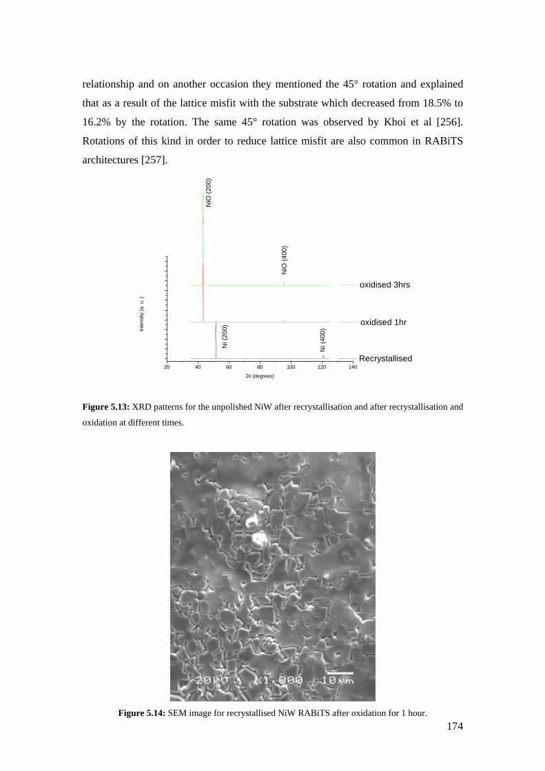
174
relationship and on another occasion they mentioned the 45° rotation and explained
that as a result of the lattice misfit with the substrate which decreased from 18.5% to
16.2% by the rotation. The same 45° rotation was observed by Khoi et al [256].
Rotations of this kind in order to reduce lattice misfit are also common in RABiTS
architectures [257].
20 40 60 80 100 120 140 Recrystallised
oxidised 1hr
oxidised 3hrsN
iO (4
00)
NiO
(200
)
Ni (
400)
Ni (
200)In
tens
ity (a
. u. )
2θ (degrees)
Figure 5.13: XRD patterns for the unpolished NiW after recrystallisation and after recrystallisation and
oxidation at different times.
Figure 5.14: SEM image for recrystallised NiW RABiTS after oxidation for 1 hour.

175
Figure 5.15: SEM image for recrystallised NiW RABiTS after oxidation for 3 hours.
Figure 5.16: A 30x30µm2 AFM image for recrystallised NiW RABiTS after oxidation for 1 hour.
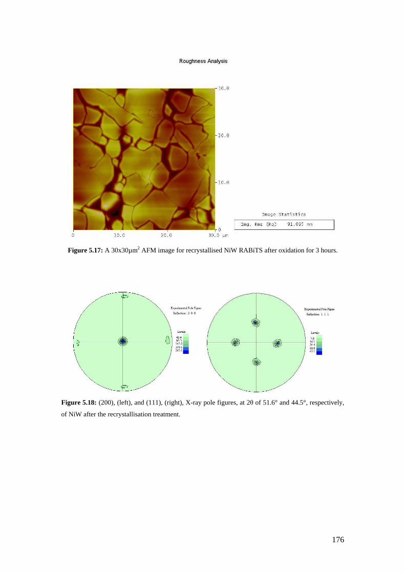
176
Figure 5.17: A 30x30µm2 AFM image for recrystallised NiW RABiTS after oxidation for 3 hours.
Figure 5.18: (200), (left), and (111), (right), X-ray pole figures, at 2θ of 51.6° and 44.5°, respectively,
of NiW after the recrystallisation treatment.

177
Figure 5.19: (200), (left), and (111), (right), X-ray pole figures, at 2θ of 43.3° and 37.3°, respectively,
of NiO oxide layer (oxidised for 1 hour) on top of the recrystallised NiW shown in Figure 5.18.
NiO was also grown on the recrystallised and polished NiW substrates. The
same texture was obtained as that for the unpolished substrates, however with a
smoother surface (about 40nm).
Before presenting MgO deposition on this NiO layer, the stability of the surface
under the conditions used for YBCO deposition by PLD was investigated first. This
was done by applying the same thermal cycle and the same atmosphere as when
YBCO will be deposited and was done on the grown NiO layer on the polished and
the unpolished recrystallised NiW substrates. Therefore, the samples were loaded in
the PLD chamber, the chamber was then pumped down to about 1.3x10⁻⁶ mbar
(1x10⁻⁶ torr), they were heated to 780°C (at a rate of 20°C/min.) under 0.6 mbar (450
mtorr) for the same period of time as when YBCO is to be deposited. The samples
were then cooled to room temperature at a rate of 10°C/min.
It was found that the texture of NiO on the unpolished surface was not changed
and this confirms the stability of the oxide layer. However, the NiO layer on the
polished substrate showed a mixed orientation after the thermal cycle (Figure 5.20). It
was clear that the texture changed from (200) to a mixed texture of (200) and (111).
This may be attributed to the mechanical stresses created on the surface of the
polished substrate during mechanical polishing which in turn disturbed the stability of
the oxide film texture at 780°C. The surface smoothness was also deteriorated from
40nm before the thermal cycle to about 65nm after the thermal cycle. Therefore, MgO
will not be deposited on such an oxide layer grown on polished substrates. Figure 5.21
is the SEM image of the recrystallised and polished NiW substrate after the thermal
cycle.
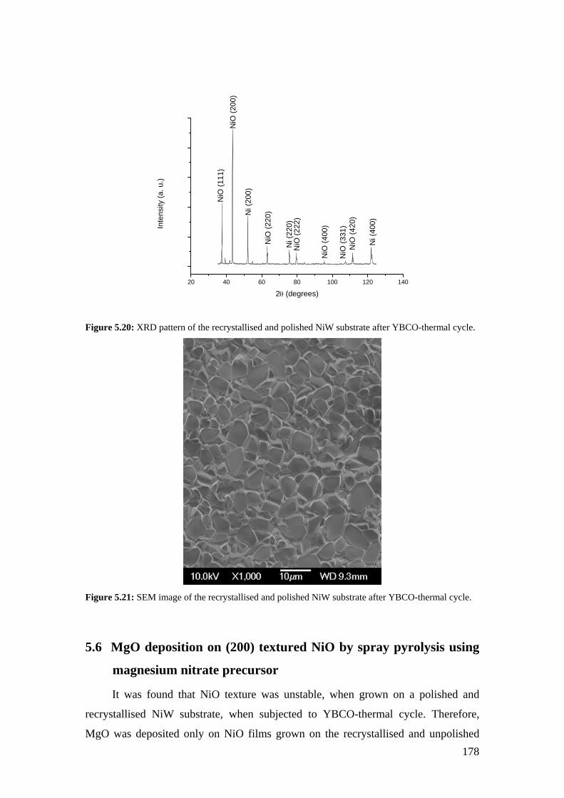
178
20 40 60 80 100 120 140
NiO
(331
)
Ni (
400)
NiO
(420
)
NiO
(400
)
NiO
(222
)N
i (22
0)
NiO
(220
)Ni (
200)
NiO
(200
)N
iO (1
11)
Inte
nsity
(a. u
.)
2θ (degrees)
Figure 5.20: XRD pattern of the recrystallised and polished NiW substrate after YBCO-thermal cycle.
Figure 5.21: SEM image of the recrystallised and polished NiW substrate after YBCO-thermal cycle.
5.6 MgO deposition on (200) textured NiO by spray pyrolysis using
magnesium nitrate precursor
It was found that NiO texture was unstable, when grown on a polished and
recrystallised NiW substrate, when subjected to YBCO-thermal cycle. Therefore,
MgO was deposited only on NiO films grown on the recrystallised and unpolished

179
NiW substrates. The oxidation of NiW substrates was done under O2 for one hour as it
gave a smoother film compared to that when using three hours.
MgO deposition was performed at 650°C for 32 minutes using 0.078M-0.468M
Mg(NO3)2.6H2O. No MgO XRD peaks were detected even when using the high
concentration of 0.468M (Figure 5.22). EDX test (at 4KV) showed the presence of
Mg and this suggests that the deposited MgO film was amorphous, although it could
be that the Mg reacted to form other phases. The particles formed on the surface
(Figure 5.23) were detected by EDX as MgO particles and this increased the
roughness of the substrate to about 170nm (Figure 5.24) compared to about 70nm
(Figure 5.16) before MgO deposition.
20 30 40 50 60 70 80
NiO
(220
)
NiO
(111
)
NiO
(200
)
Inte
nsity
(a. u
.)
2θ (degrees)
Figure 5.22: log scale XRD pattern for MgO deposition on NiO grown on unpolished and
recrystallised NiW substrate tape by spray pyrolysis at 650°C using 0.468M Mg(NO3)2.6H2O for 32
minutes.

180
Figure 5.23: SEM image for MgO deposition on NiO grown on unpolished and recrystallised NiW
substrate tape by spray pyrolysis at 650°C using 0.468M Mg(NO3)2.6H2O for 32 minutes.
Figure 5.24: A 5x5µm2 AFM image for MgO deposition on NiO grown on unpolished and
recrystallised NiW substrate tape by spray pyrolysis at 650°C using 0.468M Mg(NO3)2.6H2O for 32
minutes.
The reason for not detecting any MgO peaks was not very clear, however, it
may be attributed to the surface instability of the oxide during the spray pyrolysis

181
deposition conditions. Even when MgO deposition was applied from acetate
precursors (its thermal decomposition is discussed in section 8.2.1) at 550°C and
650°C using 0.093M and 0.279M solutions, although, no MgO peaks were detected as
well. Therefore, MgO deposition by spray pyrolysis on NiW RABiTS or on NiO was
not successful due to the surface instability of the substrate and/or the oxide layer
under the spray pyrolysis deposition conditions. Although, Ming Wei et al [54]
deposited CeO2 by the ESAVD on textured Ni tapes. However, there are some
differences in the two cases; in this work we are depositing MgO not CeO2 by spray
pyrolysis not by ESAVD. In addition to that, Ming Wei et al did not mention whether
CeO2 films were deposited directly on Ni tapes or on pre- buffered ones.

182
6 Spray pyrolysis of MgO on 310-austenitic stainless
steel using magnesium nitrate as a precursor

183
6.1 Introduction
In this chapter the deposition of MgO thin films by spray pyrolysis on wrought
polycrystalline 310-austenitic stainless steel, using magnesium nitrate as a precursor,
will be introduced. The 310-stainless steels (StSt) (100mm x100mm x 2mm) were
bought from Goodfellow. The substrates were then cut into 10mm x10mm x 2mm
using the wire electric discharge machine (WEDM). The samples were then
mechanically polished down to a roughness of 2-5 nm, and then they were cleaned in
acetone, then ethanol for 10 minutes each in an ultrasonic bath, then dried with Ar
gas. In the spray pyrolysis deposition, an Ar flow rate of 10 l/min was used, a pulse
time to interval time of 1:7 was applied; however, the deposition temperature,
deposition time, and precursor concentration were varied.
As far as we know, no reports have been found for MgO deposition on metallic
substrates by spray pyrolysis. The aim is to reduce the cost of production by using
spray pyrolysis instead of the relatively expensive methods for the buffer layer
deposition, such as electron beam evaporation [82] and pulse laser deposition [80]. As
in the previous chapter an objective of this work is to grow MgO as the only buffer
layer before YBCO deposition in an attempt to make the process a cost-effective one
by reducing the usual multi-layer buffer architecture to a single layer.
6.2 310-stainless steel substrates
The chemical composition of the 310-austenitic stainless steel substrates, as
received from the supplier, was checked using EDX (using an accelerating voltage of
20 KV) and compared to the American Iron and Steel Institute (AISI) standards
[266].
Table 6.1 shows that that the chemical composition of the substrates as received
from the supplier is within a good approximation to the AISI standards and to the one
obtained from the EDX test.

184
Table 6.1: Chemical composition of the 310-St. St.
Element
Chemical
composition, wt%
(Goodfellow)
Chemical
composition, wt%
(AISI)
Chemical
composition, wt%
(EDX, 20KV )
Cr 24-26 24-26 26.08
Ni 19-22 19-22 19.83
Mn <2 2 1.55
Si <1 1.5 0.58
C <0.25 0.25 0.22
Fe Balance Balance Balance
The surface roughness of the polished substrates, as shown from the AFM
image in Figure 6.1, shows that the roughness is in the order of 2-5nm. Figure 6.2 is
the SEM image of the substrate after polishing.
Figure 6.1: A 5x5µm2 AFM image of the mechanically polished 310-St. St substrate.

185
Figure 6.2: SEM image of the mechanically polished 310-St. St. substrate.
From the JCPDS PDF files, we could not find any XRD patterns for these
specific substrates, i.e. the 310-stainless steels substrates. Figure 6.3 shows the XRD
pattern for the 310-stainless steel substrates with the XRD peaks being indexed
according to the structure factor rule (the (111), (200) and (220) peaks are at 2θs of
43.60°, 50.85° and 74.78°, respectively). From the sequence of the peaks,
double-single, it was recognised that the structure of the 310-stainless steel is FCC
with a calculated lattice parameter of 3.58Å and having a thermal expansion
coefficient of 16-18x10-6/K as given by the supplier [267]. It was also clear from the
XRD pattern that the substrates were polycrystalline with (111) being the strongest
peak.

186
20 40 60 80
St.
St.
(220
)
St.
St.
(200
)
St.
St.
(111
)
Inte
nsity
(a. u
.)
2θ (degrees)
Figure 6.3: XRD pattern of the mechanically polished 310-St. St. substrate with the peaks being
indexed according to the structure factor rule.
6.3 Spray pyrolysis of MgO on 310-austenitic stainless using
magnesium nitrate precursor
6.3.1 Effect of deposition temperature and time on MgO film properties
MgO was spray pyrolysed on the 310-austenitic stainless steel substrates using
Mg(NO3)2.6H2O as a precursor. The deposition was done using 0.078M at different
temperatures for 32 minutes. The XRD patterns after the deposition are shown in
Figure 6.4 where it can be seen that no MgO XRD peaks were detected regardless of
the substrate temperature.

187
20 30 40 50 60 70 80
550οC 0.078M
650οC 0.078M
750οC 0.078M
Inte
nsity
(a. u
.)
2θ (degrees)
St. S
t. (1
11)
St.
St.
(200
)
St.
St.
(220
)
Figure 6.4: XRD patterns for MgO deposited on 310-St. St. using 0.078M of Mg(NO3)2.6H2O at
different temperatures for 32 minutes.
Further investigation on the deposited MgO films was made by performing an
EDX test. The results obtained suggest that Mg and O are present in almost
stoichiometric ratio. The EDX result, using an accelerating voltage of 4KV, for the
sample deposited at 650°C from 0.078M is shown in Table 6.2. From this, and from
the XRD patterns in Figure 6.4, it is suggested that the deposited MgO films were
amorphous, although it could be that the Mg reacted to form other phases.
Table 6.2: Summary of the EDX chemical composition result for the 310-St. St. deposited with
0.078M at 650°C for 32 minutes.
Element at %
O K 23.99
Mg K 19.21
Fe L 34.17
Cr L 15.41
Ni L 7.22

188
In an attempt to deposit (200) oriented MgO films, the deposition time was
increased to 96 minutes for the sample deposited at 650°C. Even by increasing the
deposition time three times more compared to those in Figure 6.4, no MgO XRD
peaks were detected as can be seen from Figure 6.5. As was the case for the sample
deposited with 0.078M at 650°C for 32 minutes (Table 6.2), the EDX result for the
sample with a deposition time of 96 minutes showed the presence of Mg and O.
Therefore, the deposited MgO film was again amorphous, although it could be that the
Mg reacted to form other phases.
10 20 30 40 50 60 70 80
650οC 0.078M 32 min.
650οC 0.078M 96 min.
St. S
t. (2
20)
St. S
t. (2
00)
St. S
t. (1
11)
Inte
nsity
(a. u
.)
2θ (degrees) Figure 6.5: XRD patterns for MgO deposited on 310-St. St. using 0.078M of Mg(NO3)2.6H2O at
650°C with different deposition times.
The SEM images for the samples deposited at different temperatures and at
different deposition times (i.e. those shown in Figure 6.4 and Figure 6.5) are shown in
Figure 6.6 to Figure 6.9. It is clear that the MgO thin film was decorating the substrate
when the temperature was higher than 550°C, where the film was copying the surface
morphology of the substrate grains. The decoration was more pronounced as the
temperature was higher than 550°C or the deposition time was higher than 32
minutes. In addition to that, the roughness increased by increasing the temperature or
the deposition time as can be seen from the SEM images (Figure 6.6 to Figure 6.9).

189
Figure 6.6: SEM image of the MgO film deposited on 310-St. St. at 550°C from a solution of 0.078M
of Mg(NO3)2.6H2O with a deposition time of 32 minutes.
Figure 6.7: SEM image of the MgO film deposited on 310-St. St. at 650°C from a solution of 0.078M
of Mg(NO3)2.6H2O with a deposition time of 32 minutes.

190
Figure 6.8: SEM image of the MgO film deposited on 310-St. St. at 750°C from a solution of 0.078M
of Mg(NO3)2.6H2O with a deposition time of 32 minutes.
Figure 6.9: SEM image of the MgO film deposited on 310-St. St. at 650°C from a solution of 0.078M
of Mg(NO3)2.6H2O with a deposition time of 96 minutes.

191
6.3.2 Effect of precursor concentration on MgO film properties
In order to grow (200) oriented MgO films, the concentration and deposition
times were increased once again. The deposition time was increased to 48 minutes
and the concentration was increased to 0.468M and 0.78M. However, as can be seen
from the XRD patterns in Figure 6.10, no MgO XRD peaks were detected. As was the
case for the samples deposited from 0.078M solution, the MgO films for the samples
deposited from 0.468M and 0.78M solutions were decorating the substrate and
copying their grain morphology (Figure 6.11 and Figure 6.12, respectively). The EDX
result, for the sample deposited from 0.468M solution (Figure 6.13 and Table 6.3),
suggests that the substrate was deposited with a stoichiometric MgO film. However,
from the EDX and XRD results, it was concluded that such a film was amorphous,
although it could be that the Mg reacted to form other phases. The MgO film
deposited from 0.78M solution was found to be amorphous as well. The EDX tests
performed on the particles (Figure 6.11 and Figure 6.12) show that such particles were
MgO.
20 30 40 50 60 70
650οC 0.78M 48 min.
650οC 0.468M 48 min.
St. S
t. (2
00)
St. S
t. (1
11)
Inte
nsity
(a. u
.)
2θ (degrees)
Figure 6.10: XRD patterns for MgO deposition on 310-St. St. at 650°C using different deposition
concentrations of Mg(NO3)2.6H2O.

192
Figure 6.11: SEM image of the MgO film deposited on 310-St. St. at 650°C from a solution of 0.468M
of Mg(NO3)2.6H2O with a deposition time of 48 minutes.
Figure 6.12: SEM image of the MgO film deposited on 310-St. St. at 650°C from a solution of 0.78M
of Mg(NO3)2.6H2O with a deposition time of 48 minutes.
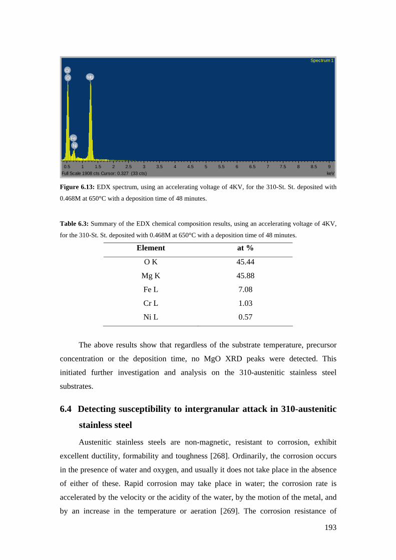
193
NiFe
O MgCr
0.5 1 1.5 2 2.5 3 3.5 4 4.5 5 5.5 6 6.5 7 7.5 8 8.5 9keVFull Scale 1908 cts Cursor: 0.327 (33 cts)
Spectrum 1
Figure 6.13: EDX spectrum, using an accelerating voltage of 4KV, for the 310-St. St. deposited with
0.468M at 650°C with a deposition time of 48 minutes.
Table 6.3: Summary of the EDX chemical composition results, using an accelerating voltage of 4KV,
for the 310-St. St. deposited with 0.468M at 650°C with a deposition time of 48 minutes.
Element at %
O K 45.44
Mg K 45.88
Fe L 7.08
Cr L 1.03
Ni L 0.57
The above results show that regardless of the substrate temperature, precursor
concentration or the deposition time, no MgO XRD peaks were detected. This
initiated further investigation and analysis on the 310-austenitic stainless steel
substrates.
6.4 Detecting susceptibility to intergranular attack in 310-austenitic
stainless steel
Austenitic stainless steels are non-magnetic, resistant to corrosion, exhibit
excellent ductility, formability and toughness [268]. Ordinarily, the corrosion occurs
in the presence of water and oxygen, and usually it does not take place in the absence
of either of these. Rapid corrosion may take place in water; the corrosion rate is
accelerated by the velocity or the acidity of the water, by the motion of the metal, and
by an increase in the temperature or aeration [269]. The corrosion resistance of

194
Stainless Steel is therefore required during spray pyrolysis of MgO due to the
relatively high temperature used during deposition and the wet environment
encountered.
Steels are said to be stainless when they resist corrosion; this is achieved by
dissolving sufficient chromium in the iron to produce a coherent, adherent, insulating
and regenerating chromium oxide protective film on the surface. It is not surprising
therefore that they are used in the harsh environments where corrosion resistance is an
important design criterion. The stainless character occurs when the concentration of
chromium exceeds about 12 wt%. However, even this is not adequate to resist
corrosion in acids such as HCl or H2SO4.
In normal conditions, austenitic stainless steels are given a high-temperature
heat-treatment, often called a solution-treatment, which gives a fully austenitic solid
solution. However, at temperatures below about 800°C, there is a tendency to
precipitate chromium-rich carbides as the alloy enters the carbide plus austenite phase
field. The carbon content in stainless steel is believed to play a key role in the
precipitation of Cr carbides. The main carbide phase is M23C6, where the 'M' stands
for a mixture of metal atoms including iron, molybdenum, chromium and manganese,
depending on the steel composition and heat-treatment. These carbides require
long-range diffusion in order to precipitate and hence can be avoided by rapid cooling
from the solution-treatment temperature. The precipitation of M23C6 and M7C3 occurs
primarily at the austenite grain surfaces which are heterogeneous nucleation sites; it
can occur in a matter of minutes at temperatures around 750°C. The chemical
composition in the vicinity of the grain boundaries can be altered by the precipitation
of the chromium-rich particles. The resulting chromium-depleted zone at the grain
boundaries makes them susceptible to intergranular anodic-attack even under
stress-free conditions. Once again, the anodic regions present a much smaller area
(grain boundaries) compared with the rest of the exposed surface which is cathodic;
the localised rate of corrosion at the boundaries is therefore greatly exaggerated. This
is the essence of sensitisation. In addition, precipitation of nitrides along the grain
boundaries, such as Cr2N, due to excess of N may also lead to a localised depletion of
Cr and hence induce localised corrosion around them [270, 271]. This situation may
also be valid during MgO deposition from the nitrate precursor.
In section 6.3, MgO was deposited on 310-stainless steel at various
temperatures, deposition times and different concentrations of the [Mg(NO3)2.6H2O]

195
precursor. However, no XRD peaks were detected for MgO and it was concluded that
the deposited MgO films were amorphous, although it could be that the Mg reacted to
form other phases. From the surface morphologies of the MgO films, when the
temperature is higher than 550°C, in Figure 6.7-Figure 6.9, Figure 6.11 and Figure
6.12, it can be seen that grooves were formed along the grain boundaries of the
substrates which were decorated by the amorphous MgO layer. Such morphologies
are similar to the morphologies encountered in sensitised austenitic stainless steels
[271-273].
At temperatures between 425oC-900οC, there is a tendency to precipitate
chromium-rich carbides mainly along the grain boundaries. The resulting
chromium-depleted zone close to the grain boundaries make them susceptible to
intergranular corrosion (Figure 6.14) [266, 273-275]. For this reason, the substrate
materials were investigated for the sensitisation effect as will be discussed in the next
section.
Figure 6.14: Mechanism of sensitisation [274].
6.4.1 ASTM A 262: practice A-oxalic acid etch of austenitic stainless
steels
The ASTM test (practice A 262) for detecting the susceptibility to intergranular
corrosion (IGC) was adopted [275]. This test detects the susceptibility to intergranular
attack associated with the precipitation of chromium carbides. It is a rapid and simple
method of identifying the specimens that are free of susceptibility to intergranular
attack by means of their etch structures.
The test requires a source of direct current and a cylindrical piece of stainless
steel, as large as the specimen to be etched, working as a cathode. The specimen to be
tested (etched) is made the anode. The solution used for etching is prepared by adding
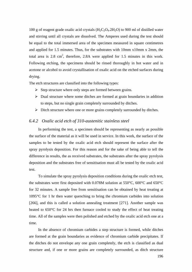
196
100 g of reagent grade oxalic acid crystals (H2C2O4.2H2O) to 900 ml of distilled water
and stirring until all crystals are dissolved. The Amperes used during the test should
be equal to the total immersed area of the specimen measured in square centimetres
and applied for 1.5 minutes. Thus, for the substrates with 10mm x10mm x 2mm, the
total area is 2.8 cm2, therefore, 2.8A were applied for 1.5 minutes in this work.
Following etching, the specimens should be rinsed thoroughly in hot water and in
acetone or alcohol to avoid crystallisation of oxalic acid on the etched surfaces during
drying.
The etch structures are classified into the following types:
Step structure where only steps are formed between grains.
Dual structure where some ditches are formed at grain boundaries in addition
to steps, but no single grain completely surrounded by ditches.
Ditch structure where one or more grains completely surrounded by ditches.
6.4.2 Oxalic acid etch of 310-austenitic stainless steel
In performing the test, a specimen should be representing as nearly as possible
the surface of the material as it will be used in service. In this work, the surface of the
samples to be tested by the oxalic acid etch should represent the surface after the
spray pyrolysis deposition. For this reason and for the sake of being able to tell the
difference in results, the as received substrates, the substrates after the spray pyrolysis
deposition and the substrates free of sensitisation must all be tested by the oxalic acid
test.
To simulate the spray pyrolysis deposition conditions during the oxalic etch test,
the substrates were first deposited with 0.078M solution at 550°C, 600°C and 650°C
for 32 minutes. A sample free from sensitisation can be obtained by heat treating at
1095°C for 1 hr then water quenching to bring the chromium carbides into solution
[266], and this is called a solution annealing treatment [271]. Another sample was
heated to 650°C for 24 hrs then furnace cooled to study the effect of heat treating
time. All of the samples were then polished and etched by the oxalic acid etch one at a
time.
In the absence of chromium carbides a step structure is formed, while ditches
are formed at the grain boundaries as evidence of chromium carbide precipitates. If
the ditches do not envelope any one grain completely, the etch is classified as dual
structure and, if one or more grains are completely surrounded, as ditch structure

197
[272]. In the oxalic acid etch test, conditions for acceptable and unacceptable etch
structures are specified. Acceptable etch structures (Figure 6.15-Figure 6.19 which
show step and dual structures) are immune to intergranular attack. Unacceptable etch
structures (Figure 6.20 which show a ditch structure) indicate that the specimen may
be subject to intergranular attack where ditches are surrounding the grains [273]. So,
from Figure 6.17-Figure 6.19, severe intergranular corrosion in 310-stainless steel,
under the deposition conditions used during spray pyrolysis, is not observed.
However, from Figure 6.18 and Figure 6.19, some carbides are still being formed as
can be seen from the grooves (ditches) formed at the grain boundaries. It can also be
noted, especially in Figure 6.18 and Figure 6.19, that the twin boundaries were not
attacked by the acid, indicating to some extent that the twin boundaries exhibit a
better corrosion resistance than the grain boundaries. X. Q. Wu et al [271] found
similar groove (or ditch) structure in 316L austenitic stainless steel after being given a
sensitisation treatment at 650°C for 2 hours. The XRD patterns did not show any
peaks corresponding to Cr precipitates in the steel but their presence caused
degradation of the corrosion resistance of grain boundaries.
Figure 6.15: SEM image after the oxalic acid test for detecting the (IGC) in as received 310-St. St.
showing a step structure.

198
Figure 6.16: SEM image after the oxalic acid test for detecting the (IGC), in 310-St. St. heated to
1095°C for 1 hr then water quenched then polished, showing a step structure.
Figure 6.17: SEM image after the oxalic acid test for detecting the (IGC), in 310-St. St. deposited with
MgO at 550°C from 0.078M solution of Mg(NO3)2.6H2O with a deposition time of 32 minutes then
removed by polishing, showing a step structure.

199
Figure 6.18: SEM image after the oxalic acid test for detecting the (IGC), in 310-St. St. deposited with
MgO at 600°C from 0.078M solution of Mg(NO3)2.6H2O with a deposition time of 32 minutes, then
removed by polishing, showing a dual structure.
Figure 6.19: SEM image after the oxalic acid test for detecting the (IGC), in 310-St. St. deposited with
MgO at 650°C from 0.078M solution of Mg(NO3)2.6H2O with a deposition time of 32 minutes then
removed by polishing, showing a dual structure.

200
Figure 6.20: SEM image after the oxalic acid test for detecting the (IGC), in 310-St. St. heated to
650°C ,without any depositions, for 24 hrs then furnace cooled and polished, showing a ditch structure.
As the surface quality of the substrates, such as roughness, cleanliness and grain
boundary grooving, play a significant role for the buffer and the YBCO growth and
also may affect the superconducting properties [61, 167, 264, 265], it was concluded
that the substrate surface is not stable for thin film deposition and that 310-St. St. is
not a good candidate as a substrate material for buffer layer deposition using the spray
pyrolysis technique due to the thermal instability of the surface during deposition at
relatively high temperature and wet environment.
201
7 Spray pyrolysis of MgO on Hastelloy C276 from
nitrate precursor

202
7.1 Introduction
This chapter is divided mainly into two. In the first part, the stability of the
substrate for thin film deposition will be investigated in terms of the susceptibility to
intergranular corrosion. In the second part of this chapter, the deposition of MgO from
a nitrate precursor, at different deposition temperatures, precursor concentrations,
deposition times, inclination angles, Ar-flow rates and different annealing treatments
will be investigated. To evaluate the performance of the MgO films, YBCO was then
deposited by PLD on top of MgO film deposited by spray pyrolysis on Hastelloy
C276. In an attempt to improve the in-plane texture of YBCO, CeO2 was also deposited
by PLD on top of MgO film deposited by spray pyrolysis on Hastelloy C276.
7.2 Susceptibility of Hastelloy C276 to intergranular corrosion
7.2.1 Introduction
Hastelloy is a non-magnetic candidate substrate material [32], which exhibits
good resistance to sea-water corrosion, excellent pitting and crevice corrosion
resistance [268], and it is has good resistance to creep, fatigue and erosion [276]. As
for 310 austenitic stainless steel (section 6.4), the corrosion resistance of Hastelloy
C276 is required during spray pyrolysis of MgO due to the relatively high temperature
used during deposition and the wet environment encountered. Therefore, before
depositing MgO films, examination of the surface stability of Hastelloy C276 for thin
film deposition was given the priority this time. This was done by applying a standard
test to study the susceptibility of Hastelloy C276 to intergranular corrosion as will be
explained in section 7.2.3.
7.2.2 Hastelloy C276 substrates
The Hastelloy C276 (HC) (100mm x100mm x 2mm) was bought from
Goodfellow. The substrates were then cut into 10mm x10mm x 2mm using the wire
electric discharge machine (WEDM). The samples were then mechanically polished
down to a roughness of 2-5 nm, and then they were cleaned in acetone, then ethanol
for 10 minutes each in an ultrasonic bath, then dried with Ar gas.
The chemical composition of the wrought Hastelloy C276 substrates, as
received from the supplier, was checked using the EDX (using an accelerating voltage
of 20 KV) and compared to the American Iron and Steel Institute (AISI) standards

203
[266]. Table 7.1 shows that the chemical composition of the substrates as received
from the supplier is, with a good approximation, close to the AISI standards and to the
one obtained from the EDX test.
Table 7.1: Chemical composition of the as received Hastelloy C276.
Element
Chemical
composition, wt%
(Goodfellow)
Chemical
composition, wt%
(AISI)
Chemical
composition, wt%
(EDX, 20KV )
Cr 13-17.5 15.5 15.67
Ni Balance 59 58
Mo 16-18 16 15.81
W 3.7-5.3 3.7 4.23
C <0.15 0.02 0.12
Fe 4.5-7 5 6.17
The surface roughness of the substrates, as shown from the AFM image in
Figure 7.1, shows that the roughness was in the order of 2-5 nm. Figure 7.2 is the
SEM image of the substrate after polishing and Figure 7.3 is the SEM image of the
sample after being polished and etched with kalling’s reagent (10 g CuCl2, 50 ml HCl,
and 50 ml ethanol) to reveal the microstructure.
Figure 7.1: A 5x5µm2 AFM image of the mechanically polished Hastelloy C276 substrate.

204
Figure 7.2: SEM image of the mechanically polished Hastelloy C276 substrate.
Figure 7.3: SEM image of the mechanically polished Hastelloy C276 substrate and etched with the
kalling’s reagent.
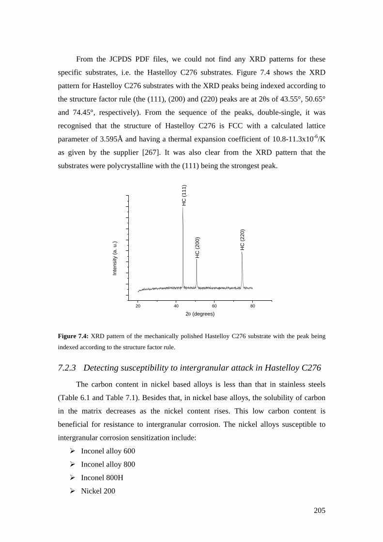
205
From the JCPDS PDF files, we could not find any XRD patterns for these
specific substrates, i.e. the Hastelloy C276 substrates. Figure 7.4 shows the XRD
pattern for Hastelloy C276 substrates with the XRD peaks being indexed according to
the structure factor rule (the (111), (200) and (220) peaks are at 2θs of 43.55°, 50.65°
and 74.45°, respectively). From the sequence of the peaks, double-single, it was
recognised that the structure of Hastelloy C276 is FCC with a calculated lattice
parameter of 3.595Å and having a thermal expansion coefficient of 10.8-11.3x10⁻⁶/K
as given by the supplier [267]. It was also clear from the XRD pattern that the
substrates were polycrystalline with the (111) being the strongest peak.
20 40 60 80
HC
(220
)
HC
(200
)
HC
(111
)
Inte
nsity
(a. u
.)
2θ (degrees)
Figure 7.4: XRD pattern of the mechanically polished Hastelloy C276 substrate with the peak being
indexed according to the structure factor rule.
7.2.3 Detecting susceptibility to intergranular attack in Hastelloy C276
The carbon content in nickel based alloys is less than that in stainless steels
(Table 6.1 and Table 7.1). Besides that, in nickel base alloys, the solubility of carbon
in the matrix decreases as the nickel content rises. This low carbon content is
beneficial for resistance to intergranular corrosion. The nickel alloys susceptible to
intergranular corrosion sensitization include:
Inconel alloy 600
Inconel alloy 800
Inconel 800H
Nickel 200
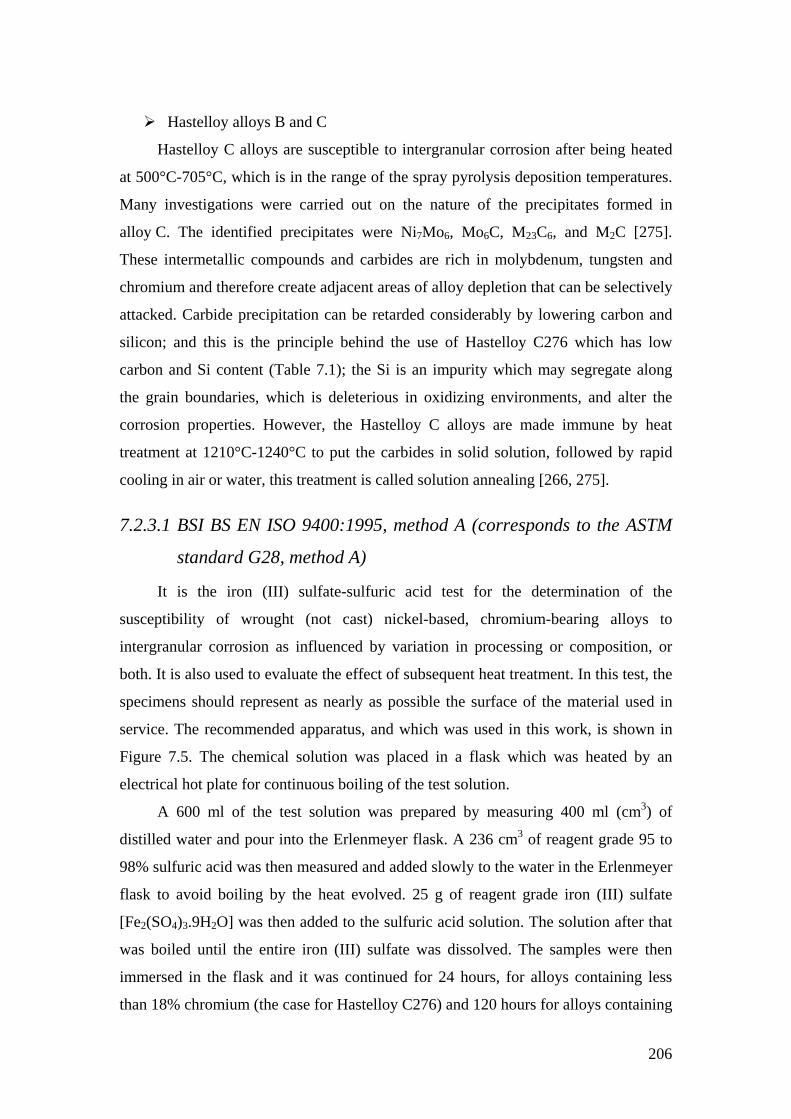
206
Hastelloy alloys B and C
Hastelloy C alloys are susceptible to intergranular corrosion after being heated
at 500°C-705°C, which is in the range of the spray pyrolysis deposition temperatures.
Many investigations were carried out on the nature of the precipitates formed in
alloy C. The identified precipitates were Ni7Mo6, Mo6C, M23C6, and M2C [275].
These intermetallic compounds and carbides are rich in molybdenum, tungsten and
chromium and therefore create adjacent areas of alloy depletion that can be selectively
attacked. Carbide precipitation can be retarded considerably by lowering carbon and
silicon; and this is the principle behind the use of Hastelloy C276 which has low
carbon and Si content (Table 7.1); the Si is an impurity which may segregate along
the grain boundaries, which is deleterious in oxidizing environments, and alter the
corrosion properties. However, the Hastelloy C alloys are made immune by heat
treatment at 1210°C-1240°C to put the carbides in solid solution, followed by rapid
cooling in air or water, this treatment is called solution annealing [266, 275].
7.2.3.1 BSI BS EN ISO 9400:1995, method A (corresponds to the ASTM
standard G28, method A)
It is the iron (III) sulfate-sulfuric acid test for the determination of the
susceptibility of wrought (not cast) nickel-based, chromium-bearing alloys to
intergranular corrosion as influenced by variation in processing or composition, or
both. It is also used to evaluate the effect of subsequent heat treatment. In this test, the
specimens should represent as nearly as possible the surface of the material used in
service. The recommended apparatus, and which was used in this work, is shown in
Figure 7.5. The chemical solution was placed in a flask which was heated by an
electrical hot plate for continuous boiling of the test solution.
A 600 ml of the test solution was prepared by measuring 400 ml (cm3) of
distilled water and pour into the Erlenmeyer flask. A 236 cm3 of reagent grade 95 to
98% sulfuric acid was then measured and added slowly to the water in the Erlenmeyer
flask to avoid boiling by the heat evolved. 25 g of reagent grade iron (III) sulfate
[Fe2(SO4)3.9H2O] was then added to the sulfuric acid solution. The solution after that
was boiled until the entire iron (III) sulfate was dissolved. The samples were then
immersed in the flask and it was continued for 24 hours, for alloys containing less
than 18% chromium (the case for Hastelloy C276) and 120 hours for alloys containing
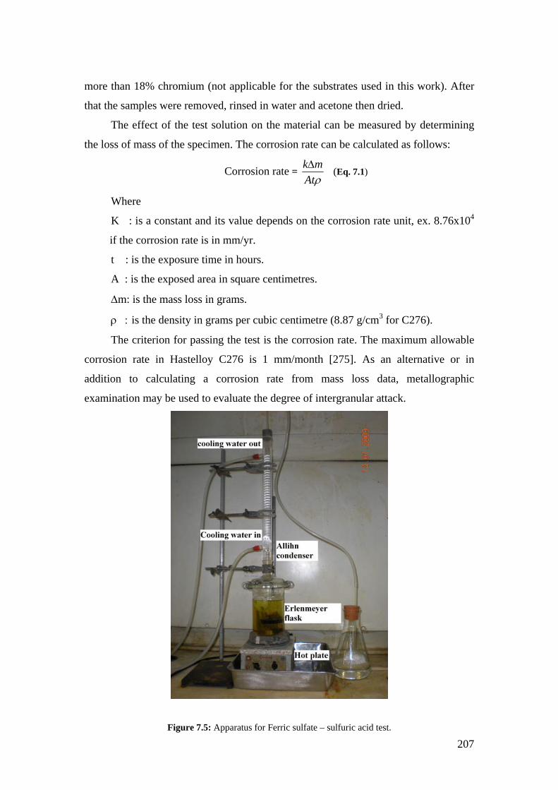
207
more than 18% chromium (not applicable for the substrates used in this work). After
that the samples were removed, rinsed in water and acetone then dried.
The effect of the test solution on the material can be measured by determining
the loss of mass of the specimen. The corrosion rate can be calculated as follows:
Corrosion rate = ρAtmkΔ
(Eq. 7.1)
Where
K : is a constant and its value depends on the corrosion rate unit, ex. 8.76x10⁴
if the corrosion rate is in mm/yr.
t : is the exposure time in hours.
A : is the exposed area in square centimetres.
Δm: is the mass loss in grams.
ρ : is the density in grams per cubic centimetre (8.87 g/cm3 for C276).
The criterion for passing the test is the corrosion rate. The maximum allowable
corrosion rate in Hastelloy C276 is 1 mm/month [275]. As an alternative or in
addition to calculating a corrosion rate from mass loss data, metallographic
examination may be used to evaluate the degree of intergranular attack.
Figure 7.5: Apparatus for Ferric sulfate – sulfuric acid test.

208
7.2.3.2 Ferric sulfate – sulfuric acid test for Hastelloy C276
In performing the test, a specimen should be representing as nearly as possible
the surface of the material as it will be used in service. In this work, the surface of the
samples to be tested by the ferric sulfate-sulfuric acid test should represent the surface
after the spray pyrolysis deposition. For this reason and for the sake of being able to
tell the difference in results, the as received substrates, the substrates after the spray
pyrolysis deposition and the substrates free of sensitisation must all be tested by the
ferric sulfate-sulfuric acid test.
To simulate the spray pyrolysis deposition conditions during the ferric
sulfate-sulfuric acid test, the substrates were first deposited with 0.078M solution at
500°C, 550°C, 600°C and 650°C for 48 minutes. A sample free from sensitisation can
be obtained by heat treating at 1215°C for 1 hr then water quenched (WQ) to bring the
chromium carbides into solution, and this is called a solution annealing [266, 275].
Another sample was heated to 650°C for 24 hrs then furnace cooled to study the effect
of heat treating time. All of the samples were then polished and subjected to the
boiling ferric sulfate-sulfuric acid test.
Table 7.2 shows the corrosion rate results in mm/month. According to the
American Society for Metals (ASM), the corrosion rate should exceed 1 mm/month
for the samples to be considered susceptible to IGC [275]. According to that, none of
the Hastelloy samples, regardless of the spray pyrolysis deposition conditions, which
were applied before the test, or the applied heat treatment, were susceptible to
intergranular corrosion; as the corrosion rate was less than 1mm/month. The highest
corrosion rate was found for the sample heated to 650°C for 24 hours then furnace
cooled, even though the corrosion rate was less than 1mm/month (0.76mm/month).
This slight increase in the corrosion rate compared to the other samples may be
attributed to the long heating time which led to the formation of some chromium
carbides at grain boundaries.

209
Table 7.2: Corrosion rates as obtained from the Ferric sulfate-sulfuric acid test.
Exposed
area (cm2)
Weight before
test (g)
Weight after
test (g)
Weight loss
(g)
Corrosion
rate
(mm/month)
As
received 2.732 1.6654 1.62490 0.0405 0.51
500°C 2.619 1.53027 1.48946 0.04081 0.53
550°C 2.775 1.61239 1.56902 0.04337 0.54
600°C 2.799 1.70467 1.65983 0.04484 0.55
650°C 2.748 1.63630 1.59240 0.0439 0.55
1215°C
(WQ) 2.743 1.66740 1.62711 0.04029 0.5
650°C
(24 hrs) 2.667 1.61126 1.55212 0.05914 0.76
The SEM images for the samples after the ferric sulfate-sulfuric acid test are
shown in Figure 7.6-Figure 7.12. From the SEM images, it can be seen that all of the
samples have the same structure except the one heated to 1215°C then water
quenched (Figure 7.7) and the one heated at 650°C for 24 hours then furnace cooled
(Figure 7.12). Those structures agree with the corrosion rate values, where the sample
heated to 650°C for 24 hours had the highest corrosion rate and the SEM image
showed that it was the most attacked one. However, the sample heated to 1215°C had
the lowest corrosion rate and the SEM image showed that it is the least attacked one.
It is known that the carbon content in stainless steel plays a key role in the
precipitation of Cr carbides [271]. By taking into consideration the low percentage of
carbon in Hastelloy C276 (0.02% max.) compared to that in 310-stainless steel
(0.25%) [266], (Table 6.1 and Table 7.1, respectively), the SEM images in Figure 7.6-
Figure 7.12 show pits formed on grain boundaries from the long contact with the
acid, not ditches or grooves as was seen in Figure 6.18-Figure 6.20, which was as a
result of the sensitisation effect due to the formation of Cr-carbides. Therefore, it was
clear that the Hastelloy under the spray pyrolysis deposition conditions used in this
study was not susceptible to IGC. Therefore, it was concluded that C276 can be used
as a substrate for MgO deposition, by spray pyrolysis, in terms of the surface stability.
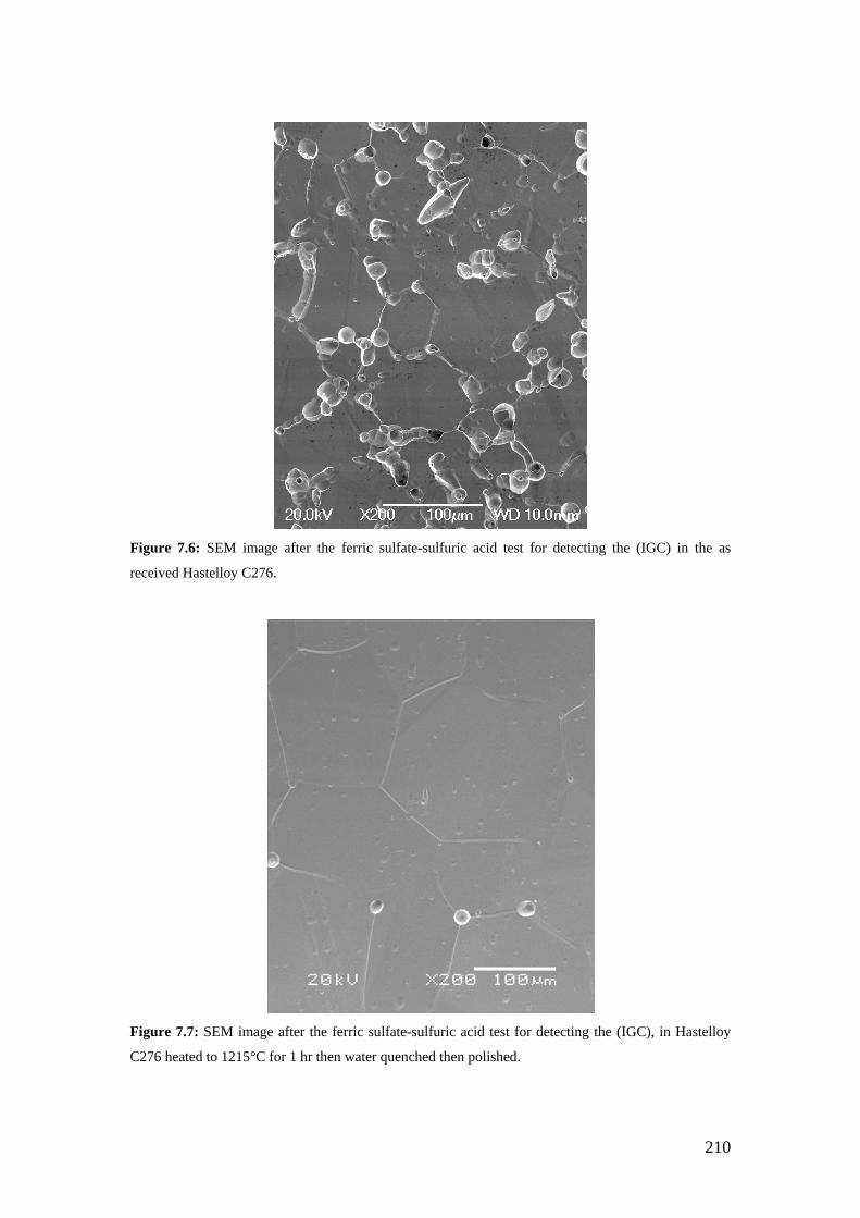
210
Figure 7.6: SEM image after the ferric sulfate-sulfuric acid test for detecting the (IGC) in the as
received Hastelloy C276.
Figure 7.7: SEM image after the ferric sulfate-sulfuric acid test for detecting the (IGC), in Hastelloy
C276 heated to 1215°C for 1 hr then water quenched then polished.

211
Figure 7.8: SEM image after the ferric sulfate-sulfuric acid test for detecting the (IGC), in Hastelloy
C276 after deposition of MgO at 500°C from 0.078M solution of Mg(NO3)2.6H2O with a deposition
time of 48 minutes which was then removed by polishing.
Figure 7.9: SEM image after the ferric sulfate-sulfuric acid test for detecting the (IGC), in Hastelloy
C276 after deposition of MgO at 550°C from 0.078M solution of Mg(NO3)2.6H2O with a deposition
time of 48 minutes which was then removed by polishing.

212
Figure 7.10: SEM image after the ferric sulfate-sulfuric acid test for detecting the (IGC), in Hastelloy
C276 after deposition of MgO at 600°C from 0.078M solution of Mg(NO3)2.6H2O with a deposition
time of 48 minutes which was then removed by polishing.
Figure 7.11: SEM image after the ferric sulfate-sulfuric acid test for detecting the (IGC), in Hastelloy
C276 after deposition of MgO at 650°C from 0.078M solution of Mg(NO3)2.6H2O with a deposition
time of 48 minutes which was then removed by polishing.
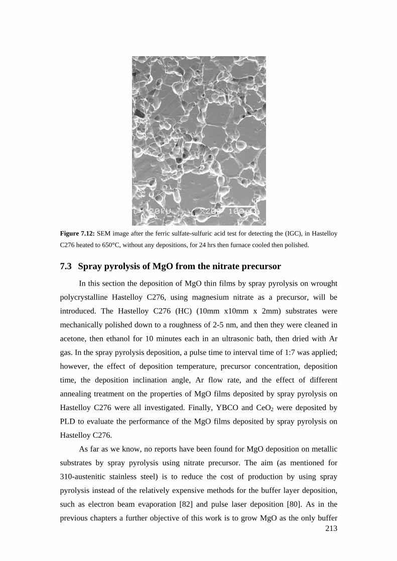
213
Figure 7.12: SEM image after the ferric sulfate-sulfuric acid test for detecting the (IGC), in Hastelloy
C276 heated to 650°C, without any depositions, for 24 hrs then furnace cooled then polished.
7.3 Spray pyrolysis of MgO from the nitrate precursor
In this section the deposition of MgO thin films by spray pyrolysis on wrought
polycrystalline Hastelloy C276, using magnesium nitrate as a precursor, will be
introduced. The Hastelloy C276 (HC) (10mm x10mm x 2mm) substrates were
mechanically polished down to a roughness of 2-5 nm, and then they were cleaned in
acetone, then ethanol for 10 minutes each in an ultrasonic bath, then dried with Ar
gas. In the spray pyrolysis deposition, a pulse time to interval time of 1:7 was applied;
however, the effect of deposition temperature, precursor concentration, deposition
time, the deposition inclination angle, Ar flow rate, and the effect of different
annealing treatment on the properties of MgO films deposited by spray pyrolysis on
Hastelloy C276 were all investigated. Finally, YBCO and CeO2 were deposited by
PLD to evaluate the performance of the MgO films deposited by spray pyrolysis on
Hastelloy C276.
As far as we know, no reports have been found for MgO deposition on metallic
substrates by spray pyrolysis using nitrate precursor. The aim (as mentioned for
310-austenitic stainless steel) is to reduce the cost of production by using spray
pyrolysis instead of the relatively expensive methods for the buffer layer deposition,
such as electron beam evaporation [82] and pulse laser deposition [80]. As in the
previous chapters a further objective of this work is to grow MgO as the only buffer

214
layer before YBCO deposition in an attempt to make the process a cost-effective one
by reducing the usual multi-layer buffer architecture to a single layer.
It is to be mentioned that X-ray scans for the MgO films deposited by spray
pyrolysis on Hastelloy C276 detected only MgO (200) peaks from the MgO film.
Therefore, we could not quantify the level of texture as no other peaks were detected
to reference to. Accordingly, it was assumed that an increase in the intensity of MgO
(200) peak reflects an improvement in texture
7.4 Effect of deposition temperature on MgO film properties
Magnesium nitrate [Mg(NO3)2.6H2O] as a precursor was used to deposit MgO
by spray pyrolysis on Hastelloy C276 substrates. The deposition was done using
0.078M at different temperatures for 32 minutes and using an Ar flow rate of 10
l/min. The XRD patterns after the deposition are shown in Figure 7.13 where it can be
seen that no MgO XRD peaks were detected regardless of the substrate temperature.
20 30 40 50 60 70
600οC 0.078M 32 min.
750οC 0.078M 32 min.
550οC 0.078M 32 min.
650οC 0.078M 32 min.
HC
(200
)
HC
(111
)
Inte
nsity
(a. u
.)
2θ (degrees) Figure 7.13: XRD patterns for MgO deposition on Hastelloy C276 using 0.078M of Mg(NO3)2.6H2O
at different temperatures for 32 minutes.
The SEM images in Figure 7.14-Figure 7.16 show microstructures which are
very similar to the one obtained for MgO deposition on Si single crystal from 0.078M
solution at 650°C (Figure 4.5). This confirms that the microstructure of the deposited
MgO films depends on the used substrate; similar microstructures were obtained on
different substrates but by using different deposition temperatures. The SEM image
for the films deposited at 750°C (Figure 7.17) show a different microstructure where

215
the grain boundaries of the substrate were revealed (compare to Figure 7.3). This can
be attributed to the thermal etching effect, not due to any sensitisation effects. As
from the boiling acid test it was found that the substrates were not susceptible to
sensitisation. The revealing of the grain boundaries at high temperatures was even
seen during pulsed laser deposition of YBCO on NiW RABiTS by Y L Cheung et al
[259, 261]. The thermal etching effect on Ni RABiTS was also seen by others [32,
264, 265].
The EDX tests performed on the films deposited on Hastelloy C276 at 550°C to
650°C show the presence of Mg. However, no MgO XRD peaks were detected
(Figure 7.13) and this suggests that the deposited MgO films were amorphous. It was
believed that this was due to the low thickness of the deposited MgO films. For MgO
deposition on Si, it was found that the texture of MgO improved with increasing
thickness. More details on thickness will be found in section 7.8. It will be found that
thinner films were obtained on C276 compared to those obtained on Si single crystals,
and this shows the dependence of MgO film deposition on the used substrate. MgO
and other films were deposited by researchers on ceramic substrates; they found that
amorphous films were obtained at low thicknesses and that the texture developed with
thickness [114, 140, 146, 147, 154, 158, 160-162]. O. Renault and M. Labeau [146]
found that MgO films thinner than 150 nm were amorphous. Stryckmans et al [142]
found that the texture of MgO deposited on alumina substrates from magnesium
acetylacetonate precursor developed with thickness. James R. Groves et al [242]
found the same behaviour for MgO films deposited by ion beam assisted deposition
(IBAD). Elidrissi B et al [154] found that CeO2 films prepared on glass substrates at
low temperatures by spray pyrolysis were amorphous. Joseph Prince J et al [140]
found that low precursor concentration resulted in the formation of amorphous In2O3
films.
The EDX test for the sample deposited at 750°C suggested a ratio of Mg:O of
about 1:10. This would be attributed to the high deposition temperature where the
lifetime required for evaporation would be shorter compared to that when using
0.078M at 650°C. Besides that, it was believed that at high temperatures, the gas
convection from the substrates will be more pronounced which makes the residence
time of droplets in the spray pyrolysis system shorter; where the time will not be
enough for nucleation and growth to proceed to completion. This combined effect of
shorter evaporation lifetime and higher gas convections results in the formation of
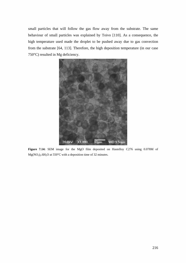
216
small particles that will follow the gas flow away from the substrate. The same
behaviour of small particles was explained by Toivo [110]. As a consequence, the
high temperature used made the droplet to be pushed away due to gas convection
from the substrate [64, 113]. Therefore, the high deposition temperature (in our case
750°C) resulted in Mg deficiency.
Figure 7.14: SEM image for the MgO film deposited on Hastelloy C276 using 0.078M of
Mg(NO3)2.6H2O at 550°C with a deposition time of 32 minutes.

217
Figure 7.15: SEM image for the MgO film deposited on Hastelloy C276 using 0.078M of
Mg(NO3)2.6H2O at 600°C with a deposition time of 32 minutes.
Figure 7.16: SEM image for the MgO film deposited on Hastelloy C276 using 0.078M of
Mg(NO3)2.6H2O at 650°C with a deposition time of 32 minutes.
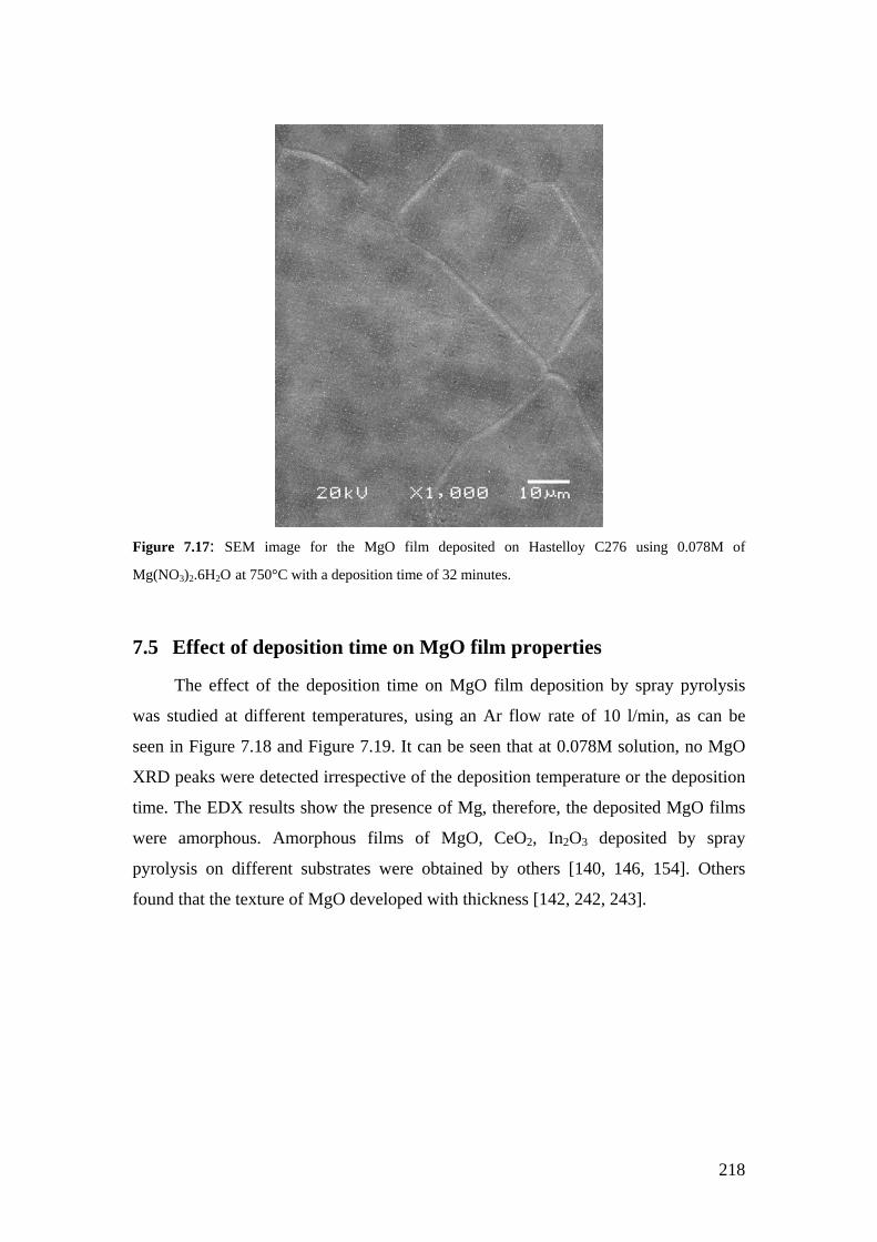
218
Figure 7.17: SEM image for the MgO film deposited on Hastelloy C276 using 0.078M of
Mg(NO3)2.6H2O at 750°C with a deposition time of 32 minutes.
7.5 Effect of deposition time on MgO film properties
The effect of the deposition time on MgO film deposition by spray pyrolysis
was studied at different temperatures, using an Ar flow rate of 10 l/min, as can be
seen in Figure 7.18 and Figure 7.19. It can be seen that at 0.078M solution, no MgO
XRD peaks were detected irrespective of the deposition temperature or the deposition
time. The EDX results show the presence of Mg, therefore, the deposited MgO films
were amorphous. Amorphous films of MgO, CeO2, In2O3 deposited by spray
pyrolysis on different substrates were obtained by others [140, 146, 154]. Others
found that the texture of MgO developed with thickness [142, 242, 243].

219
20 30 40 50 60 70
550οC 0.078M 64 min.
550οC 0.078M 32 min.H
C (2
00)
HC
(111
)
Inte
nsity
(a. u
.)
2θ (degrees) Figure 7.18: XRD patterns for MgO deposition on Hastelloy C276 using 0.078M of Mg(NO3)2.6H2O
at 550°C and at different deposition time.
20 30 40 50 60 70
650οC 0.078M 96 min.
650οC 0.078M 32 min.
HC
(200
)
HC
(111
)
Inte
nsity
(a. u
.)
2θ (degrees) Figure 7.19: XRD patterns for MgO deposition on Hastelloy C276 using 0.078M of Mg(NO3)2.6H2O
at 650°C and at different deposition time.
The SEM image for the films deposited at 550°C for 64 minutes (Figure 7.20)
was almost the same as the one deposited for 32 minutes (Figure 7.14) except it has
some particles being formed on the surface. The MgO film deposited at 650°C (Figure
7.21) show the formation of overgrown particles as was the case for the MgO film

220
deposited on Si single crystal at 700°C (Figure 4.7), but it was more pronounced in
the case of MgO deposition on Hastelloy C276. By increasing the deposition time, the
particles have enough time to grow regardless of the substrate temperature and this
may explain the formation of particles at 550°C and 650°C (Figure 7.20 and Figure
7.21) when increasing the deposition time to 64 minutes and 96 minutes, respectively,
relative the films deposited at the same temperatures but for 32 minutes (Figure 7.14
and Figure 7.16).
The formation of amorphous MgO films even by increasing the deposition time
gave an indication that the thickness of the deposited films was still low. This implied
that the used concentration was not high enough to develop a textured MgO film by
the deposition of thick films.
Figure 7.20: SEM image for the MgO film deposited on Hastelloy C276 using 0.078M of
Mg(NO3)2.6H2O at 550°C with a deposition time of 64 minutes.

221
Figure 7.21: SEM image for the MgO film deposited on Hastelloy C276 using 0.078M of
Mg(NO3)2.6H2O at 650°C with a deposition time of 96 minutes.
7.6 Effect of precursor concentration on MgO film properties
The deposition of MgO films on Hastelloy C276 was then performed at higher
concentrations, using 0.468M and 0.78M solutions. The used Ar flow rate was 10
l/min, and the deposition was done at different temperatures and deposition times as
can be seen from the XRD patterns in Figure 7.22. This time MgO peaks were
successfully observed. A weak MgO (200) peak, the only detected one, started to
appear normal to the substrate surface. The MgO peaks were indexed according to the
JCPDS PDF file 00-045-0946 where MgO (200) is at 2θ of 42.9°. The thermal
expansion coefficients of Hastelloy C276 and MgO are 10.8-11.3x10⁻⁶ /°C and 13.8 x
10-6/°C, respectively [143, 267]. The lattice parameter for MgO is 4.2112Å and for
Hastelloy C276, as calculated from Bragg’s law, is 3.5952Å and this gives a lattice
mismatch of 17.1%. This explains the shift of MgO peaks in Figure 7.22 to 43.15°;
however, this shift is not much compared to that obtained when depositing MgO on Si
single crystals. It can be seen from Figure 7.22 that the peak intensity increased by
increasing the deposition time, the deposition temperature or by increasing the
concentration. However, this was at the expense of the film smoothness as can be seen

222
from the SEM images (Figure 7.23-Figure 7.28) and Figure 7.29. The smoothest films
were deposited at 650°C for 32 and 48 minutes using 0.468M Mg(NO3)2.6H2O which
show an RMS of about 20 nm (Figure 7.30 and Figure 7.31). An AFM section profile
image is shown in Figure 7.32 for MgO films deposited from 0.468M solution at
650°C for 32 minutes. When comparing Figure 7.23 and Figure 7.30 to Figure 7.32, it
can be seen that the surface is homogenous and smooth and most of the film was
located on the same layer as can be seen from Figure 7.32. The same was also
observed for the film deposited from 0.468M solution at 650°C for 48 minutes.
However, all of the other MgO films shown in Figure 7.22 show particles or grains
which were located on different layers relative to the rest of the film.
According to the deposition modes of spray pyrolysis [83], the smooth surface
for both films ( i.e. the ones deposited using 0.468M at 650°C for 32 and 48 minutes)
were deposited according to the third mode of deposition; when the thermal
decomposition of dry precipitates starts on their way to the substrate. However, by
increasing the deposition time more than 48 minutes, by increasing the deposition
temperature to 700°C or by increasing the concentration to 0.78M, overgrown
particles were formed on the surface (Figure 7.25-Figure 7.28), which led to an
increase in the roughness (Figure 7.29). The fourth mode of deposition leads to the
formation of particles on the surface by increasing the temperature, where the full
thermal decomposition takes place outside the substrate and only finely divided solid
product arrives at the substrate surface; therefore, at 700°C, the deposition was carried
out according to the fourth mode of deposition. It is also to be pointed out that the
actual working mode depends not only on the substrate temperature, but also on the
temperature of the working surrounding [83]. By increasing the deposition time to 64
minutes (Figure 7.25) and 96 minutes (Figure 7.26) the growth of the particles
dominates the nucleation, leading to the formation of overgrown particles. However,
no sound explanation was found to relate this behaviour with the type of the
deposition mode that might be applied to this situation and further investigation is
required. The lifetime required for evaporation increases by increasing the amount of
solute in the droplet [110]; therefore, by increasing the concentration to 0.78M, the
time is not enough to evaporate both the solvent and the solute, a situation similar to
that encountered in the second mode of deposition where dry precipitates come to the
surface [83].

223
40 42 44 46 48 50 52 54
650oC 0.468M 32 min. 650oC 0.468M 48 min. 650oC 0.468M 64 min. 650oC 0.468M 96 min.
650oC 0.780M 48 min. 700oC 0.468M 48 min.
MgO
(200
)
HC
(200
)
HC
(111
)
Inte
nsity
(a. u
.)
2θ (degrees)
Figure 7.22: XRD patterns for MgO deposition on Hastelloy C276 using 0.468M and 0.78M of
Mg(NO3)2.6H2O at different deposition temperatures and different deposition times.
Figure 7.23: SEM image for the MgO film deposited on Hastelloy C276 using 0.468M of
Mg(NO3)2.6H2O at 650°C for 32 minutes.

224
Figure 7.24: SEM image for the MgO film deposited on Hastelloy C276 using 0.468M of
Mg(NO3)2.6H2O at 650°C for 48 minutes.
Figure 7.25: SEM image for the MgO film deposited on Hastelloy C276 using 0.468M of
Mg(NO3)2.6H2O at 650°C for 64 minutes.
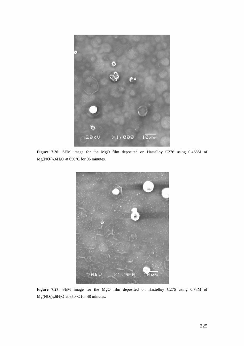
225
Figure 7.26: SEM image for the MgO film deposited on Hastelloy C276 using 0.468M of
Mg(NO3)2.6H2O at 650°C for 96 minutes.
Figure 7.27: SEM image for the MgO film deposited on Hastelloy C276 using 0.78M of
Mg(NO3)2.6H2O at 650°C for 48 minutes.
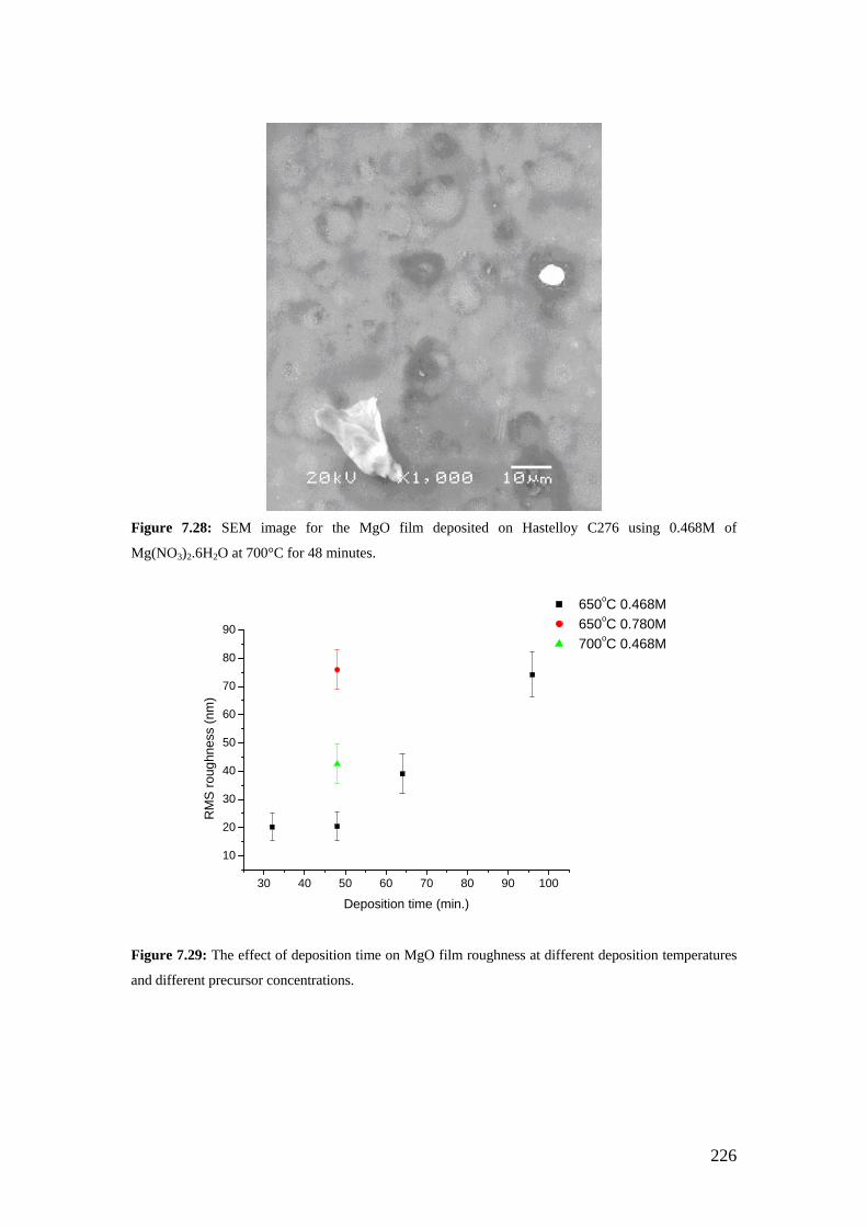
226
Figure 7.28: SEM image for the MgO film deposited on Hastelloy C276 using 0.468M of
Mg(NO3)2.6H2O at 700°C for 48 minutes.
30 40 50 60 70 80 90 100
10
20
30
40
50
60
70
80
90
RM
S ro
ughn
ess
(nm
)
Deposition time (min.)
650oC 0.468M 650oC 0.780M 700oC 0.468M
Figure 7.29: The effect of deposition time on MgO film roughness at different deposition temperatures
and different precursor concentrations.
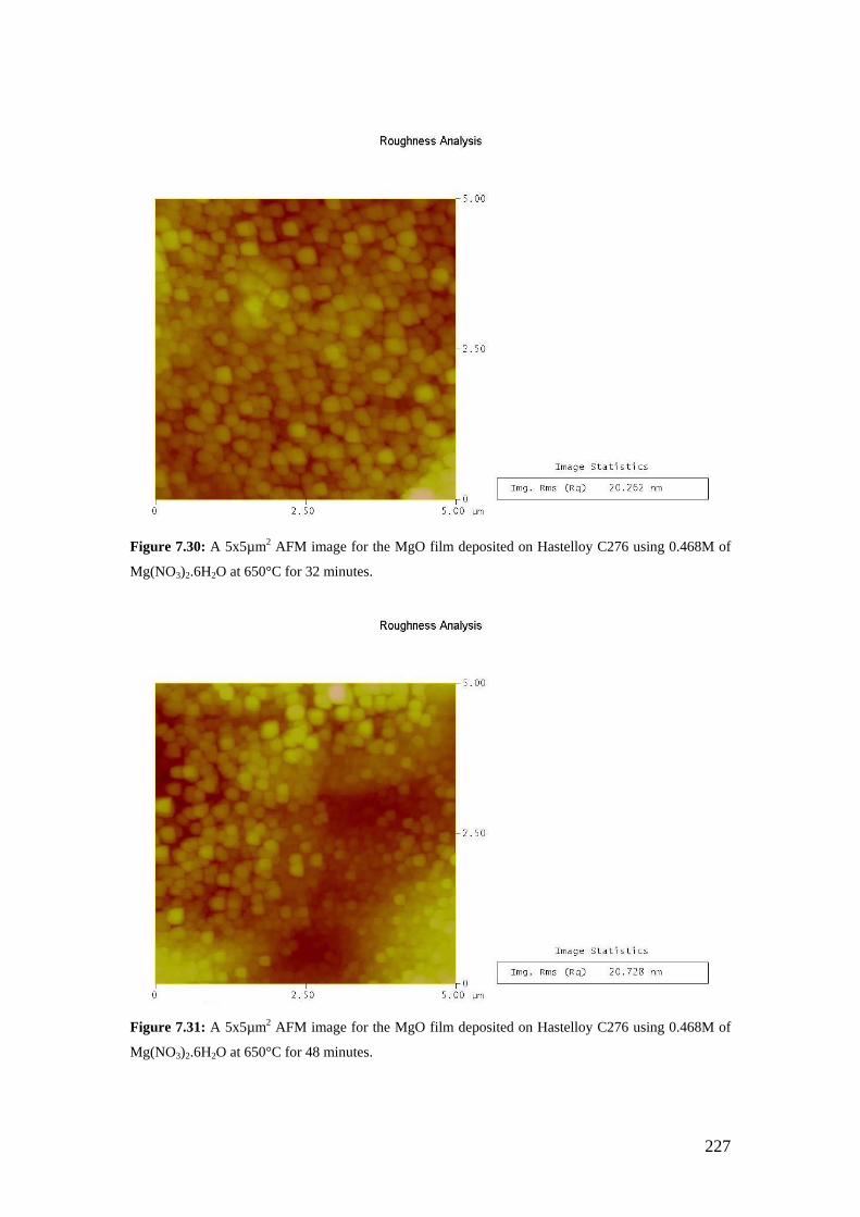
227
Figure 7.30: A 5x5µm2 AFM image for the MgO film deposited on Hastelloy C276 using 0.468M of
Mg(NO3)2.6H2O at 650°C for 32 minutes.
Figure 7.31: A 5x5µm2 AFM image for the MgO film deposited on Hastelloy C276 using 0.468M of
Mg(NO3)2.6H2O at 650°C for 48 minutes.

228
Figure 7.32: AFM section profile image for the MgO film deposited on Hastelloy C276 using 0.468M
of Mg(NO3)2.6H2O at 650°C for 32 minutes.
The EDX results, using an accelerating voltage of 4KV, suggest that all of the
films (shown in Figure 7.22) were almost stoichiometric MgO. An example is shown
in Figure 7.33 and Table 7.3 for the sample deposited at 700°C for 48 minutes from
0.468M solution. The particles were nearly stoichiometric MgO as well.
Mo Cr Cr
Fe
Ni Mo
CrO
Mg
1 2 3 4 5 6 7 8 9 10 11 12 13 14keVFull Scale 23602 cts Cursor: 0.312 (128 cts)
Spectrum 1
Figure 7.33: EDX spectrum, using an accelerating voltage of 4KV, for the Hastelloy C276 deposited
with 0.468M at 700°C with a deposition time of 48 minutes.
229
Table 7.3: Summary of the EDX chemical composition results, using an accelerating voltage of 4KV,
for the Hastelloy C276 deposited with 0.468M at 700°C with a deposition time of 48 minutes.
Element at %
O K 47.21
Mg K 45.25
Fe L 0.7
Cr L 2.78
Ni L 1.63
Mo L 2.43
The texture of MgO was not strong as can be expected from the XRD patterns
in Figure 7.22. This was confirmed from the X-ray pole figure measurements. An
MgO (200) pole figure measurement for the sample deposited at 650°C for 48
minutes from 0.468M solution is shown in Figure 7.34. It can be seen that there is a
weak out-of-plane texture and no in-plane texture (no definite poles were obtained at
the circumference but a ring was obtained instead).
Figure 7.34: : (200) X-ray pole figure, at 2θ of 43.15°, of the MgO film deposited at 650°C from a
solution of 0.468M for 48 minutes.
In an attempt to improve the texture of the MgO (200) peak, a double deposition
was made. This means that the sample was deposited under certain conditions, left to
be furnace cooled to room temperature, then deposited again at the same conditions.
This was done at 650°C for 48 minutes each using 0.468M solution. The XRD pattern
in Figure 7.35 show that the intensity of MgO peak increased by the double
deposition. This was almost similar to increasing the deposition time to 96 minutes

230
(Figure 7.22). If it is assumed that the thickness of MgO film increased with
increasing the deposition time, then it can be concluded that the texture improved
slightly with thickness. Similar behaviour was found by other researchers [142, 146,
175]. More details on thickness are found in section 7.8. However, this slight
improvement in texture with the double deposition was at the expense of the surface
smoothness as can be seen from the SEM and AFM images in Figure 7.36 and Figure
7.37, respectively compared to the film deposited at 650°C from 0.468M for 48
minutes (Figure 7.31).
40 45 50 55
650oC 0.468M 48 min. Double deposition
650oC 0.468M 48 min.
MgO
(200
)
HC
(200
)
HC
(111
)
Inte
nsity
(a. u
.)
2θ (degrees)
Figure 7.35: XRD patterns for MgO deposition on Hastelloy C276 showing the double deposition
effect using 0.468M Mg(NO3)2.6H2O at 650°C for 48 minutes.
Figure 7.36: SEM image for MgO on Hastelloy C276 with the double deposition using 0.468M
Mg(NO3)2.6H2O at 650°C for 48 minutes.
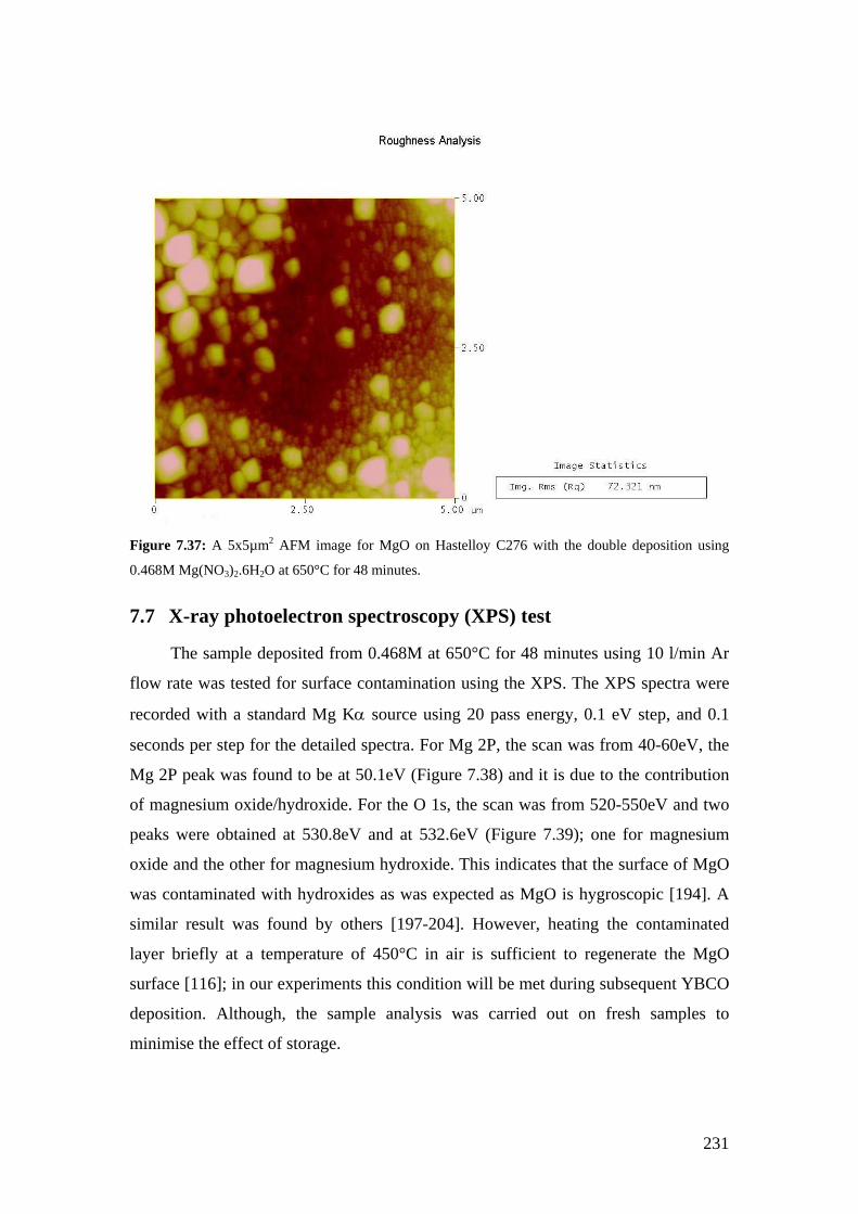
231
Figure 7.37: A 5x5µm2 AFM image for MgO on Hastelloy C276 with the double deposition using
0.468M Mg(NO3)2.6H2O at 650°C for 48 minutes.
7.7 X-ray photoelectron spectroscopy (XPS) test
The sample deposited from 0.468M at 650°C for 48 minutes using 10 l/min Ar
flow rate was tested for surface contamination using the XPS. The XPS spectra were
recorded with a standard Mg Kα source using 20 pass energy, 0.1 eV step, and 0.1
seconds per step for the detailed spectra. For Mg 2P, the scan was from 40-60eV, the
Mg 2P peak was found to be at 50.1eV (Figure 7.38) and it is due to the contribution
of magnesium oxide/hydroxide. For the O 1s, the scan was from 520-550eV and two
peaks were obtained at 530.8eV and at 532.6eV (Figure 7.39); one for magnesium
oxide and the other for magnesium hydroxide. This indicates that the surface of MgO
was contaminated with hydroxides as was expected as MgO is hygroscopic [194]. A
similar result was found by others [197-204]. However, heating the contaminated
layer briefly at a temperature of 450°C in air is sufficient to regenerate the MgO
surface [116]; in our experiments this condition will be met during subsequent YBCO
deposition. Although, the sample analysis was carried out on fresh samples to
minimise the effect of storage.

232
40 45 50 55 60
Mg 2P eV=50.1 (oxide and hydroxide)
Mg source40-60eV0.1eV step, 0.1 sec. dwell20 E pass
Inte
nsity
(a. u
.)
Binding Energy (a. u.)
Figure 7.38: XPS spectrum for the MgO thin film deposited on Hastelloy C276 substrate using
0.468M Mg(NO3)2.6H2O at 650οC for 48 min. showing the Mg 2P.
525 530 535
O 1S eV=532.6 (hydroxide)
O 1S eV=530.8 (oxide)
Mg source520-550eV0.1eV step, 0.1 sec. dwell 20 E pass
Inte
nsity
(a. u
.)
Binding Energy (eV)
Figure 7.39: XPS spectrum for the MgO thin film deposited on Hastelloy C276 substrate using
0.468M Mg(NO3)2.6H2O at 650οC for 48 min. showing the O 1S.
7.8 Effect of deposition parameters on MgO film thickness
The thickness measurements for the MgO films deposited on metallic
substrates, i.e. Hastelloy C276, was not straight forward. Three methods were tried for
the thickness measurements, using a high resolution SEM. The first one was to cut a
cross section of the sample with the spark machine followed by mechanical polishing.
However, this process increased the thickness of the films as the sample was
submerged in oil. The second method was to mount the samples and polish them
through at least one third of the sample width. This resulted sometimes in polishing

233
away of the thin film as well. In other occasions, smearing was the result of the
mechanical polishing process which made the thickness measurement not accurate.
The third method was to stick a special kind of tape on the thin film followed by
milling the back of the substrate down to half of its thickness. The sample was then
bent and the tape was removed taking with it the thin film from the bent area. The
areas of the thin film next to the removed tape were now exposed and can be used to
measure the thickness. However, this process was not very reliable as the film was
usually destroyed during the milling process due to overheating of the tape. Therefore,
studying the effect of the thickness on MgO films was not feasible on metallic
substrates. A non destructive thickness measurement using Ellipsometry was also
applied; however this method was not accurate for thicknesses in the range of 200 nm,
besides thickness measurements for MgO and YBCO films simultaneously made the
measurement process rather complex and inaccurate. After many trials, thickness
measurement by mechanically polishing the sample deposited at 650°C from a
solution of 0.468M for 32 minutes, using an Ar flow rate of 10 l/min, was achieved as
can be seen in Figure 7.40 which shows a 0.262 μm thick MgO film. This gives a
deposition rate of 10.92 Å/sec (2620Å/240sec.). This deposition rate is lower than the
deposition rate obtained for MgO films deposited on Si from 0.078M at 650°C with
zero inclination angle. This confirms that film deposition by the spray pyrolysis
technique is a function of substrate material, precursor concentration, and
temperature. Unfortunately, it was not successful to measure the thickness for any of
the samples deposited from the 0.078M solution.

234
Figure 7.40: SEM cross section for MgO film spray pyrolysed on Hastelloy C276 using 0.468M
Mg(NO3)2.6H2O at 650οC for 32 minutes.
It was found, when depositing MgO films on Si substrates that the texture
improved with increasing thickness and the thickness was found to increase with
increasing the concentration. Therefore, it was believed that at low thicknesses (as
was the case when depositing MgO on C276 using 0.078M solution), the MgO texture
was not developed yet and amorphous films were obtained. Therefore no MgO XRD
peaks were detected for the samples deposited from the 0.078M solution irrespective
of the deposition temperature (Figure 7.13) or the deposition time (Figure 7.18 and
Figure 7.19) as the concentration was low enough that sufficiently thick films for the
growth of textured MgO was not obtainable. However, by increasing the
concentration to 0.468M, sufficiently thick film was deposited and this resulted in the
deposition of MgO with a weak (200) peak. Amorphous films of MgO, CeO2, In2O3
deposited by spray pyrolysis on different substrates were obtained by others [140,
146, 154]. Others found that the texture of MgO develops with thickness [142, 183,
242]. When the concentration was increased to 0.468M, the thickness increased and
the texture was developed leading to the detection of MgO peaks (Figure 7.22). O.
Renault and M. Labaeu [146] deposited MgO on glass substrates using the aerosol
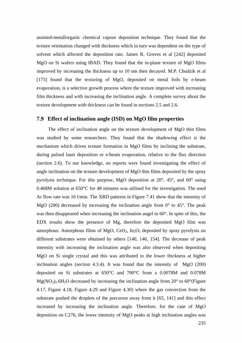
235
assisted-metallorganic chemical vapour deposition technique. They found that the
texture orientation changed with thickness which in turn was dependent on the type of
solvent which affected the deposition rate. James R. Groves et al [242] deposited
MgO on Si wafers using IBAD. They found that the in-plane texture of MgO films
improved by increasing the thickness up to 10 nm then decayed. M.P. Chudzik et al
[175] found that the texturing of MgO, deposited on metal foils by e-beam
evaporation, is a selective growth process where the texture improved with increasing
film thickness and with increasing the inclination angle. A complete survey about the
texture development with thickness can be found in sections 2.5 and 2.6.
7.9 Effect of inclination angle (ISD) on MgO film properties
The effect of inclination angle on the texture development of MgO thin films
was studied by some researchers. They found that the shadowing effect is the
mechanism which drives texture formation in MgO films by inclining the substrate,
during pulsed laser deposition or e-beam evaporation, relative to the flux direction
(section 2.6). To our knowledge, no reports were found investigating the effect of
angle inclination on the texture development of MgO thin films deposited by the spray
pyrolysis technique. For this purpose, MgO deposition at 20°, 45°, and 60° using
0.468M solution at 650°C for 48 minutes was utilised for the investigation. The used
Ar flow rate was 10 l/min. The XRD patterns in Figure 7.41 show that the intensity of
MgO (200) decreased by increasing the inclination angle from 0° to 45°. The peak
was then disappeared when increasing the inclination angel to 60°. In spite of this, the
EDX results show the presence of Mg, therefore the deposited MgO film was
amorphous. Amorphous films of MgO, CeO2, In2O3 deposited by spray pyrolysis on
different substrates were obtained by others [140, 146, 154]. The decrease of peak
intensity with increasing the inclination angle was also observed when depositing
MgO on Si single crystal and this was attributed to the lower thickness at higher
inclination angles (section 4.3.4). It was found that the intensity of MgO (200)
deposited on Si substrates at 650°C and 700°C from a 0.0078M and 0.078M
Mg(NO3)2.6H2O decreased by increasing the inclination angle from 20° to 60°(Figure
4.17, Figure 4.18, Figure 4.29 and Figure 4.30) where the gas convection from the
substrate pushed the droplets of the precursor away from it [65, 141] and this effect
increased by increasing the inclination angle. Therefore, for the case of MgO
deposition on C276, the lower intensity of MgO peaks at high inclination angles was

236
also attributed to the low thickness of MgO. Others found that the texture of MgO
developed with thickness [142, 242].
However, it is to be noted in this work that inclining the substrate led to untilted
MgO films with (200) direction parallel to the substrate normal and did not result in
the shadowing effect which was observed for MgO and YSZ films deposited by ISD
method using PLD and e-beam evaporation [39-41, 49, 50, 53, 167, 169, 173-175,
177-183]. One more point should be mentioned. As was said before, MgO can be
deposited by inclined substrate deposition (ISD) using e-beam evaporation [173, 174].
By this method, the MgO film had the (200) with the c-axis being tilted from the
substrate normal due to the shadowing effect [173-175]. The deposited YBCO film on
top of that MgO also grows with the (00l) being tilted from the substrate normal,
which has led to low Jc values. Higher Jc and Tc values are obtained by growing
untilted YBCO films by depositing YSZ and CeO2 buffers on top of the tilted MgO
film [169, 176, 177]. In this work MgO was deposited from nitrate precursor by
inclining the substrate relative to the nozzle. This led to untilted MgO films with (200)
direction parallel to the substrate normal; no shadowing effect was observed.
However, this was at the expense of MgO (200) peak intensity. In all cases, spray
pyrolysis gave MgO (200) peaks parallel to the substrate normal whether ISD was
utilised or not. YBCO films grown on top of MgO deposited by spray pyrolysis (as
will be seen later in this chapter) had the (006) of YBCO // (200) of MgO. Thus, spray
pyrolysis offers an alternative method of depositing a single MgO buffer layer with no
tilting for later YBCO deposition.
40 42 44 46 48 50 52 54
650oC 0.468M 48 min. 60o
650oC 0.468M 48 min. 45o
650oC 0.468M 48 min. 20o
650oC 0.468M 48 min. 0o
MgO
(200
)
HC
(200
)
HC
(111
)
Inte
nsity
(a. u
.)
2θ (degrees) Figure 7.41: XRD patterns for MgO deposition on Hastelloy C276 using 0.468M Mg(NO3)2.6H2O at
650°C for 48 minutes and at different inclination angles.

237
Figure 7.42-Figure 7.45 show that the roughness decreased with increasing the
inclination angel from 20° to 60°; similar behaviour was found for MgO deposition on
Si single crystals (Figure 4.31). This behaviour can be attributed to pushing of
droplets of the precursor away from the substrates, and by increasing the inclination
angle, smoother films were obtained. However, for MgO deposition on Si, the RMS
of the film deposited with no inclination angle was rougher than the ones deposited
with an inclination angle. A different situation was encountered when depositing
MgO on Hastelloy C276. At zero inclination angle, the surface roughness was about
20nm, and by increasing the inclination angle to 20°, the surface roughness increased
to about 48nm then decreased by increasing the inclination angle to 45° and 60°. This
increase in the roughness at 20° may be attributed to a flow turbulence at the substrate
surface leading to the formation of particles and hence to an increase in the roughness.
This turbulence decreased by increasing the inclination angle, and therefore to a
decrease in the roughness values. This behaviour was not really understood and needs
further investigation. Rachel E. Koritala et al [185] found that for the case of biaxially
textured MgO films deposited by ISD using e-beam evaporation on Hastelloy C
substrates that high roughness values was obtained at low and high inclination angles
and the lowest roughness values were obtained for inclination angles of 20°-55°
where the roughness was not affected by the inclination angle in this range.
0 10 20 30 40 50 60
0
10
20
30
40
50
60
RM
S ro
ughn
ess
(nm
)
Inclination angle (degrees)
Figure 7.42: The effect of inclination angle on the film roughness of MgO films deposited from 0.468M
solution at 650°C for 48 minutes.
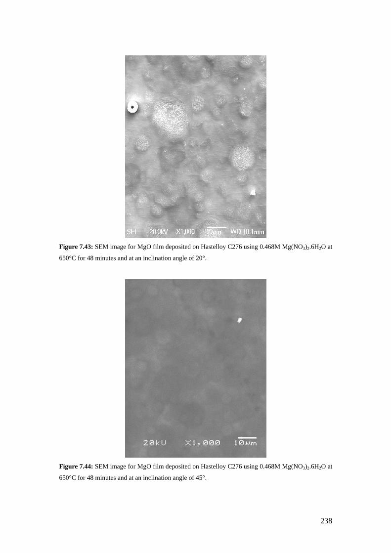
238
Figure 7.43: SEM image for MgO film deposited on Hastelloy C276 using 0.468M Mg(NO3)2.6H2O at
650°C for 48 minutes and at an inclination angle of 20°.
Figure 7.44: SEM image for MgO film deposited on Hastelloy C276 using 0.468M Mg(NO3)2.6H2O at
650°C for 48 minutes and at an inclination angle of 45°.

239
Figure 7.45: SEM image for MgO film deposited on Hastelloy C276 using 0.468M Mg(NO3)2.6H2O at
650°C for 48 minutes and at an inclination angle of 60°.
It is known that ISD deposition is applied, either by PLD or e-beam, to grow
MgO thin films to improve the in plane texture for YBCO deposition. However, from
Figure 7.41, it can be seen that the MgO (200) peak is not tilted relative to the
substrate normal. This means that the ISD deposition by spray pyrolysis is not giving
the shadowing effect observed by others. In Spray pyrolysis, the ISD is just affecting
the crystallinity, roughness and thickness of the deposited MgO films.
7.10 Effect of Ar flow rate on MgO film properties
The effect of Ar flow rate on the spray pyrolysis deposition of MgO was
investigated using 5 l/min, 10 l/min, and 15 l/min. The depositions were made using
0.468M solution at 650°C for 48 minutes. The XRD patterns in Figure 7.46 show that
low Ar flow rate (5l/min.) did not result in any MgO peaks. The EDX results (Figure
7.47 and Table 7.4) show the presence of Mg, this suggests that an amorphous MgO
film was obtained when using an Ar flow rate of 5 l/min. This was assumed to be as a
result of the low thickness of the deposited MgO film when using low Ar flow rates.
Amorphous films of MgO, CeO2, In2O3, SnO2 deposited by spray pyrolysis on
different substrates were obtained by others [140, 146, 154, 162]. Others found that
the texture of MgO developed with thickness [142, 242]. However, by increasing the

240
flow rate to 10 l/min and 15 l/min, only MgO (200) peak was detected. The high flow
rate (15 l/min) has no effect on the quality of the texture as the MgO peak was not
improved compared to that when using an Ar flow rate of 10 l/min. This is in
disagreement with what found by Xiaorong Fu et al [72] and O. Renault and M.
Labeau [146]. They found that the flow rate changed the preferred orientation. This
was also found by others for different films [144, 145]. Pavlopoulos D. also found a
change of the preferred orientation by changing the flow rate in the case of depositing
CeO2 on borosilicate glass. Joseph Prince J et al [140] found that crystallinity changed
with the flow rate in the case of depositing In2O3. In addition to that, in this work the
high flow rate (15 l/min) did not improve the intensity of MgO (200) peak and this
was attributed to the saturation effect. C. H. Lee and C. S. Huang deposited In2O3 by
spray pyrolysis on Si wafers using InCl3-methanol solution as the source material
[158], they found that at high flow rates, the growth rate was slow due to the reactant
saturation effect. Other researchers [86] found that, for MgO films deposited on Si
(100) substrates by electrostatic spray pyrolysis, the growth rate decreased with
increasing the substrate temperature, others [114] found that, for ZnO films deposited
on glass substrates by spray pyrolysis, at high temperatures the deposition rate was
constant (saturated) where the growth rate is mass transport controlled; the reaction
kinetics are so fast that the surface reaction finally becomes controlled by mass
transfer of the reactants, and the concentration of the reactants on the surface is the
limiting parameter.
42 44 46 48 50 52
Inte
nsity
(a. u
.)
2θ (degrees)
MgO
(200
)H
C (1
11)
HC
(200
)
650oC 0.468M 48 min. 5l/min
650oC 0.468M 48 min. 10l/min
650oC 0.468M 48 min. 15l/min
Figure 7.46: XRD patterns for MgO deposited on Hastelloy C276 using 0.468M Mg(NO3)2.6H2O at
650°C for 48 minutes and at different Ar flow rates.

241
Figure 7.47: EDX spectrum, using an accelerating voltage of 4KV, for the Hastelloy C276 deposited
with 0.468M at 650°C with a deposition time of 48 minutes and using an Ar flow rate of 5l/min.
Table 7.4: Summary of the EDX chemical composition results, using an accelerating voltage of 4KV,
for the Hastelloy C276 deposited with 0.468M at 650°C with a deposition time of 48 minutes and using
an Ar flow rate of 5l/min.
Element at %
O K 25.19
Mg K 30.68
Ni L 26.92
Cr L 8.85
Mo L 4.51
Fe L 3.29
W M 0.56
The SEM images (Figure 7.24, Figure 7.48) and Figure 7.49 show that the
smoothest film was obtained when using an Ar flow rate of 10 l/min and this was
confirmed by the RMS reading obtained from the AFM as shown in Figure 7.50. On
the one hand, the high flow rate (15 l/min) means more precursor material will reach
the substrate, so it resembles increasing the concentration, where the time is not
enough to evaporate both the solute and the solvent, which in turn leads to a rough
MgO films. On the other hand, at low flow rate (5l/min), fewer precursor droplets
arrive at the substrate; hence the growth rate may dominate the nucleation which in
turn gives rough surfaces as well. Therefore, it was found that the optimum flow rate
is 10 l/min which gives detectable MgO peaks and smoothest MgO films.
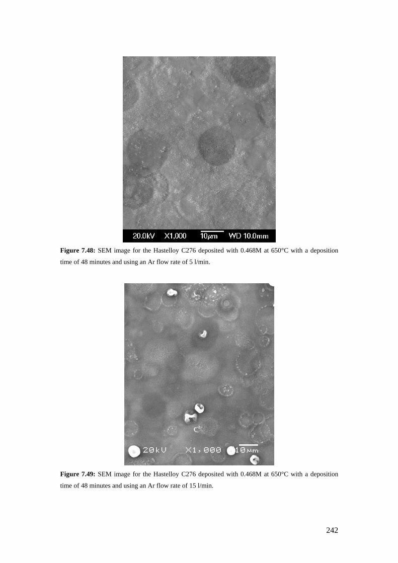
242
Figure 7.48: SEM image for the Hastelloy C276 deposited with 0.468M at 650°C with a deposition
time of 48 minutes and using an Ar flow rate of 5 l/min.
Figure 7.49: SEM image for the Hastelloy C276 deposited with 0.468M at 650°C with a deposition
time of 48 minutes and using an Ar flow rate of 15 l/min.

243
5 10 15
0
10
20
30
40
50
60
RM
S ro
ughn
ess
(nm
)
Ar flow rate (l/min)
Figure 7.50: The effect of Ar flow rate on the film roughness of MgO film deposited from 0.468M
solution at 650°C for 48 minutes.
7.11 Effect of annealing on the texture of MgO films
YBCO films deposited on annealed MgO buffers/substrates had improved
in-plane texture and superconducting properties [191-193]. Therefore, an attempt to
improve the texture of MgO films, annealing in different environments, at different
temperatures and different annealing times were performed.
7.11.1 Annealing under O2 atmosphere
The annealing experiments were carried out in a tube furnace rated to 1200°C.
Pure oxygen was supplied from a compressed gas cylinder through copper tubing. The
gas flow was controlled and was set at 100 ml/min for a furnace volume of 1630ml.
Before heating, the oxygen was open for one hour which means that the furnace
volume was replaced 3.7 times. The heating was carried out at a rate of 300°C/hr.
After heating to the required temperature and holding for the required time, the
furnace was switched off to allow the samples to be furnace cooled under O2
atmosphere as well. Figure 7.51 shows the XRD patterns for the sample deposited at
650°C for 48 minutes from a 0.468M solution after being annealed under O2
atmosphere at different temperatures and times. A narrow XRD scan is given in
Figure 7.52. It can be seen that annealing at temperatures of 400°C-650°C for three
hours did not affect the texture of the MgO (200) peak. The surface morphology and
roughness were the same as that before the annealing (Figure 7.24 and Figure 7.29).

244
This was expected as the annealing temperatures did not exceed the deposition
temperatures used during spray pyrolysis. This also confirms the stability of MgO
film up to 650°C even under O2 atmosphere. However, when the annealing
temperature was increased to 800°C for a deposition time of three hours and 1000°C
for a deposition time of three and five hours, other oxides started to appear (Figure
7.51). Those oxides were mainly chromium and nickel oxides indexed according to
the JCPDS PDF files 00-032-0285 and 00-004-0835, respectively. The oxides were
more pronounced by annealing at 1000°C for three and five hours. Some other peaks
could not be indexed and were referred to as complex oxides. At 800°C, the MgO
(200) was a little improved but this was at the expense of substrate oxidation and
roughness as will be seen below.
20 30 40 50 60 70 80
* * complex oxides**
**
NiO
(111
)
* * NiO
(220
)
650oC 0.468M O2 1000oC 3hrs
650oC 0.468M O2 800oC 3hrs
650oC 0.468M O2 650oC 3hrs
650oC 0.468M O2 600oC 3hrs
650oC 0.468M O2 400oC 3hrs
650oC 0.468M
HC
(200
)
HC
(111
)N
iO (2
00)
MgO
(200
)
CrO
3 (11
1)
650oC 0.468M O2 1000oC 5hrs
Inte
nsity
(a. u
.)
2θ (degrees) Figure 7.51: XRD patterns for Hastelloy substrates deposited with MgO from 0.468M at 650°C for 48
minutes after O2 anneal at different temperatures and times.

245
42 45 48 51
* complex oxides
*
650oC 0.468M O2 1000oC 3hrs
650oC 0.468M O2 800oC 3hrs
650oC 0.468M O2 650oC 3hrs
650oC 0.468M O2 600oC 3hrs
650oC 0.468M O2 400oC 3hrs
650oC 0.468M
HC
(200
)
HC
(111
)N
iO (2
00)
MgO
(200
) 650oC 0.468M O2 1000oC 5hrs In
tens
ity (a
. u.)
2θ (degrees) Figure 7.52: XRD patterns with a narrow scan for the Hastelloy substrates deposited with MgO from
0.468M at 650°C for 48 minutes after O2 anneal at different temperatures and times.
The SEM images for the samples annealed at 800°C and 1000°C for three hours
are shown in Figure 7.53 and Figure 7.54, respectively. It can be seen that the surface
roughness increased by annealing. It was 20 nm for the sample before annealing
(Figure 7.31) and became 63 nm for the sample annealed at 800°C for three hours and
130 nm for the sample annealed at 1000°C for three hours. The EDX test at 4KV
showed an increase in the Cr and Ni content in addition to the presence of Mg, and
this can be used to suggest the presence of oxides.
From this, it is clear that annealing up to 650C was not improving the texture
nor deteriorating the MgO film. However, annealing at 800°C-1000°C affected the
surface stability by the oxidation of the substrate.

246
Figure 7.53: SEM image for the Hastelloy substrate deposited with MgO at 650°C for 48 minutes from
0.468M solution then annealed at 800°C under O2 for three hours.
Figure 7.54: SEM image for the Hastelloy substrate deposited with MgO at 650°C for 48 minutes from
0.468M solution then annealed at 1000°C under O2 for three hours.

247
To study the effect of annealing on MgO films deposited with higher
concentration, the annealing was applied to the samples deposited from a 0.78M
solution at 650°C and for 48 minutes. The same procedures used for annealing the
samples deposited from the 0.468M solution were exactly used to anneal the samples
deposited from the 0.78M solution. Figure 7.55 shows the XRD patterns for the
samples after being annealed under O2 atmosphere at different temperatures and
times. A narrow XRD scan is given in Figure 7.56. It can be seen that annealing at
temperatures of 400°C-650°C for three hours did not affect the texture of the MgO
(200) peak. The surface morphology and roughness were the same as before the
annealing (Figure 7.27 and Figure 7.29). This was expected as the annealing
temperatures did not exceed the deposition temperature during spray pyrolysis. This
also confirms the stability of MgO film up to 650°C even under O2 atmosphere.
Therefore, annealing at 400°C-650°C did not play a role in improving the texture of
MgO (200) and this was also obtained when using 0.468M. However, when the
annealing temperature was increased to 800°C for a deposition time of three hours, an
increase in the intensity of MgO (200) was observed with no evidence of any oxides
being detected. This may be attributed to the higher concentration of the precursor
which in turn gives a thicker MgO layer which protected the substrate from oxidation.
However, this slight improvement in the texture was at the expense of surface
roughness as can be seen from the SEM and AFM images in Figure 7.57 and Figure
7.58, respectively, where the roughness is 130 nm compared to about 75nm (Figure
7.29) before annealing. This increase in roughness was due to the high annealing
temperature under O2 flow and the high precursor concentration. This may enhance
diffusion processes in the MgO film leading to the formation of rough background in
addition to the formation of MgO particles (Figure 7.57) which was confirmed by an
EDX test. Oxides started to appear when the annealing temperature increased to
1000°C for annealing time of three and five hours (Figure 7.55). The same oxides
were formed when annealing the samples deposited from 0.468M solution (Figure
7.51). Those oxides were mainly chromium and nickel oxides indexed according to
the JCPDS PDF files 00-032-0285 and 00-004-0835, respectively. The oxides were
more pronounced by annealing at 1000C for five hours. Some other peaks could not
be indexed and were referred to as complex oxides. The SEM image for the sample
annealed at 1000°C for three hours is shown in Figure 7.59 which shows a very rough

248
surface. The EDX test showed an increase in the Cr and Ni content in addition to the
presence of Mg, and this can be used to suggest the presence of oxides.
From this, it is clear that annealing up to 650C was not improving the texture
nor deteriorating the MgO film irrespective of the precursor concentration used for
depositing MgO films. However, for the precursor concentration of 0.78M, annealing
at 800°C, showed a slight improvement in the intensity of MgO (200) but this was at
the expense of roughness. Annealing at 1000°C affected the surface stability by the
oxidation of the substrate.
20 30 40 50 60 70
** complex oxides***
**
*
NiO
(111
)
NiO
(220
)
650oC 0.78M O2 800oC 3hrs
650oC 0.78M O2 650oC 3hrs
MgO
(200
)
650oC 0.78M O2 600oC 3hrs
650oC 0.78M O2 400oC 3hrs
HC
(200
)
HC
(111
)N
iO (2
00)
CrO
3 (1
11)
650oC 0.78M
650oC 0.78M O2 1000oC 3hrs
650oC 0.78M O2 1000oC 5hrs
Inte
nsity
(a. u
.)
2θ (degrees) Figure 7.55: XRD patterns for the Hastelloy substrates deposited with MgO from 0.78M at 650°C for
48 minutes after O2 anneal at different temperatures and times.
42 45 48 51 54
* complex oxides*
650oC 0.78M O2 800oC 3hrs
650oC 0.78M O2 650oC 3hrs
MgO
(200
)
650oC 0.78M O2 600oC 3hrs
650oC 0.78M O2 400oC 3hrs
HC
(200
)
HC
(111
)
NiO
(200
)
650oC 0.78M
650oC 0.78M O2 1000oC 3hrs
650oC 0.78M O2 1000oC 5hrs
Inte
nsity
(a. u
.)
2θ (degrees) Figure 7.56: XRD patterns with a narrow scan for the Hastelloy substrates deposited with MgO from
0.78M at 650°C for 48 minutes after O2 anneal at different temperatures and times.

249
Figure 7.57: SEM image for the Hastelloy substrate deposited with MgO at 650°C for 48 minutes from
0.78M solution then annealed at 800°C under O2 for three hours.
Figure 7.58: A 5x5µm2 AFM image for the Hastelloy substrate deposited with MgO at 650°C for 48
minutes from 0.78M solution then annealed at 800°C under O2 for three hours.

250
Figure 7.59: SEM image for the Hastelloy substrate deposited with MgO at 650°C for 48 minutes from
0.78M solution then annealed at 1000°C under O2 for three hours.
7.11.2 Annealing under vacuum
It was found that high temperature annealing under O2 resulted in substrate
oxidation. Therefore, to protect the substrate from oxidation, high temperature
annealing will be done in an O2-free environment. This suggests doing the annealing
under vacuum.
The vacuum annealing experiments were carried out in a tube furnace connected
to pumping system; which consists of rotary and turbo pumps. The furnace was rated
to 1200°C. Before heating, the system was pumped down to about 5x10⁻⁷ mbar
(3.75x10⁻⁷ torr). The heating was carried out at a rate of 300C°/hr. After heating to the
required temperature and holding for the required time, the furnace was switched off
to allow the samples to be furnace cooled under vacuum atmosphere as well.
Figure 7.60 shows the XRD patterns for the samples deposited at 650°C for 48
minutes from a 0.468M solution after being annealed under vacuum (~ 2x10⁻⁶ mbar)
at different temperatures and times. A narrow XRD scan is given in Figure 7.61. It
can be seen that up to 800°C with annealing time of three hours, no oxides were
formed but at the same time, no improvement in the MgO (200) texture was obtained.
The surface morphology and roughness were the same as that before annealing
(Figure 7.24 and Figure 7.31). This confirms that the MgO film is stable under

251
vacuum atmosphere up to 800°C which is good for later YBCO deposition which is
carried out under 450 mtorr O2 at 780°C as will be seen in section 7.12. By increasing
the annealing temperature to 1000°C, the MgO (200) peak disappeared, and the SEM
image (Figure 7.62) for the sample annealed at 1000°C for three hours shows that the
MgO film was severely affected where grain boundaries of the substrate were
revealed as a result of thermal etching. The EDX test showed that the formed particles
were MgO (Figure 7.63 and Table 7.5). However, the area between the particles
showed Mg deficiency (Figure 7.64 and Table 7.6). The surface roughness of the
sample increased from 20 nm before annealing (Figure 7.31) to 64.8 nm after
annealing (Figure 7.65). This increase in roughness was due to the high annealing
temperature. This may enhance diffusion processes to occur in the MgO film leading
to the formation of rough background in addition to the formation of MgO particles.
As was the case when annealing MgO films deposited from 0.468M solution,
annealing for the films deposited from 0.78M solution had no effect on the texture and
smoothness between 650°C-800°C. However, rough surfaces and Mg deficiency were
noticed when annealing at 1000°C.
20 30 40 50 60 70 80
650oC 0.468M Vac. 1000oC 3hrs
650oC 0.468M Vac. 800oC 3hrs
650oC 0.468M Vac. 1000oC 5hrs
650oC 0.468M
650oC 0.468M Vac. 650oC 3hrs
HC
(200
)
HC
(111
)M
gO (2
00)
Inte
nsity
(a. u
.)
2θ (degrees)
Figure 7.60: XRD patterns for the Hastelloy substrates deposited with MgO from 0.468M at 650°C for
48 minutes after vacuum anneal at different temperatures and times.

252
42 44 46 48 50 52 54
650oC 0.468M Vac. 1000oC 3hrs
650oC 0.468M Vac. 800oC 3hrs
650oC 0.468M Vac. 1000oC 5hrs
650oC 0.468M
650oC 0.468M Vac. 650oC 3hrs
HC
(200
)
HC
(111
)M
gO (2
00)
Inte
nsity
(a. u
.)
2θ (degrees)
Figure 7.61: XRD patterns with a narrow scan for the Hastelloy substrates deposited with MgO from
0.468M at 650°C for 48 minutes after vacuum anneal at different temperatures and times.
Figure 7.62: SEM image for the Hastelloy substrate deposited with MgO at 650°C for 48 minutes from
0.468M solution then annealed at 1000°C under vacuum for three hours.

253
Figure 7.63: EDX spectrum, using an accelerating voltage of 4KV, for the particles formed on
Hastelloy C276 deposited with 0.468M at 650°C with a deposition time of 48 minutes after being
annealed at 1000°C under vacuum for 3 hours.
Table 7.5: Summary of the EDX chemical composition results, using an accelerating voltage of 4KV,
for the particles formed on Hastelloy C276 deposited with 0.468M at 650°C with a deposition time of
48 minutes after being annealed at 1000°C under vacuum for 3 hours.
Element at %
O K 48.33
Mg K 51.23
Ni L 0.44
Figure 7.64: EDX spectrum, using an accelerating voltage of 4KV, for the area between particles
formed on Hastelloy C276 deposited with 0.468M at 650°C with a deposition time of 48 minutes after
being annealed at 1000°C under vacuum for 3 hours.

254
Table 7.6: Summary of the EDX chemical composition results, using an accelerating voltage of 4KV,
for the area between particles formed on Hastelloy C276 deposited with 0.468M at 650°C with a
deposition time of 48 minutes after being annealed at 1000°C under vacuum for 3 hours.
Element at %
O K 41.91
Mg K 26.7
Cr L 10.65
Fe L 1.42
Ni L 14.32
Mo L 3.94
W M 1.06
Figure 7.65: A 5x5µm2 AFM image for the Hastelloy substrate deposited with MgO at 650°C for 48
minutes from 0.468M solution then annealed at 1000°C under vacuum for three hours.
To study the effect of high temperature annealing (1000°C) under vacuum and
its relation to Mg deficiency, MgO single crystals were annealed under the same
conditions, i.e. under vacuum and at 1000°C for three hours.
Figure 7.66 shows the XRD patterns for MgO single crystal before and after
vacuum annealing at 1000°C for three hours. It was clear that no change happened
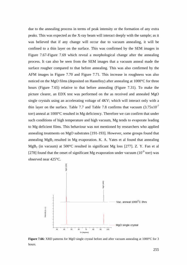
255
due to the annealing process in terms of peak intensity or the formation of any extra
peaks. This was expected as the X-ray beam will interact deeply with the sample; as it
was believed that if any change will occur due to vacuum annealing, it will be
confined to a thin layer on the surface. This was confirmed by the SEM images in
Figure 7.67-Figure 7.69 which reveal a morphological change after the annealing
process. It can also be seen from the SEM images that a vacuum anneal made the
surface rougher compared to that before annealing. This was also confirmed by the
AFM images in Figure 7.70 and Figure 7.71. This increase in roughness was also
noticed on the MgO films (deposited on Hastelloy) after annealing at 1000°C for three
hours (Figure 7.65) relative to that before annealing (Figure 7.31). To make the
picture clearer, an EDX test was performed on the as received and annealed MgO
single crystals using an accelerating voltage of 4KV; which will interact only with a
thin layer on the surface. Table 7.7 and Table 7.8 confirms that vacuum (3.75x10⁻⁷
torr) anneal at 1000°C resulted in Mg deficiency. Therefore we can confirm that under
such conditions of high temperature and high vacuum, Mg tends to evaporate leading
to Mg deficient films. This behaviour was not mentioned by researchers who applied
annealing treatments on MgO substrates [191-193]. However, some groups found that
annealing MgB2 resulted in Mg evaporation. K. A. Yates et al found that annealing
MgB2 (in vacuum) at 500°C resulted in significant Mg loss [277]. Z. Y. Fan et al
[278] found that the onset of significant Mg evaporation under vacuum (10-9 torr) was
observed near 425°C.
30 40 50 60 70 80 90 100
Vac. anneal 1000OC 3hrs
MgO single crystal
Inte
nsity
(a. u
.)
2θ (degrees)
MgO
(200
)
MgO
(400
)
Figure 7.66: XRD patterns for MgO single crystal before and after vacuum annealing at 1000°C for 3
hours.

256
Figure 7.67: SEM image of the as received MgO single crystal.
Figure 7.68: SEM image of the as received MgO single crystal after vacuum anneal at 1000°C for 3
hours.
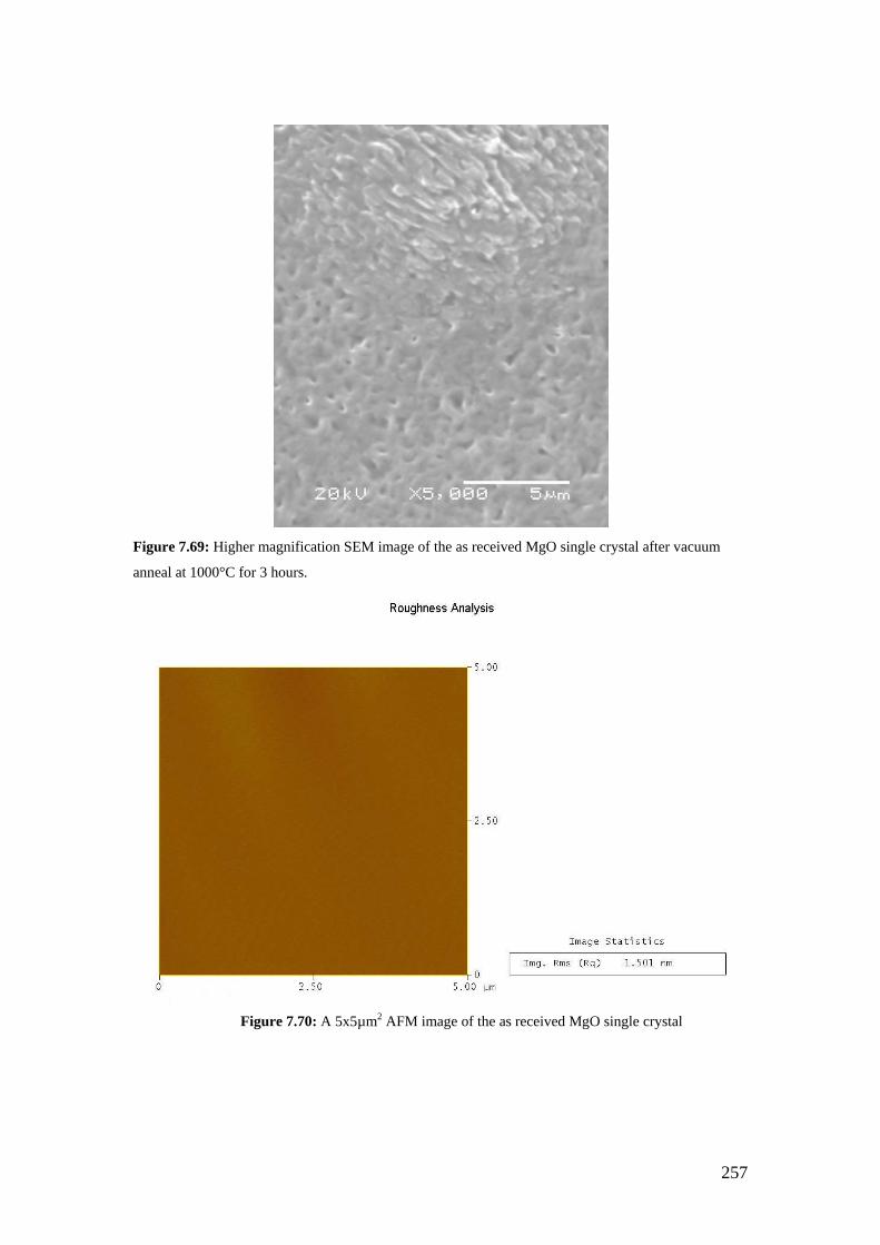
257
Figure 7.69: Higher magnification SEM image of the as received MgO single crystal after vacuum
anneal at 1000°C for 3 hours.
Figure 7.70: A 5x5µm2 AFM image of the as received MgO single crystal

258
Figure 7.71: A 5x5µm2 AFM image of the as received MgO single crystal after vacuum anneal at
1000°C for 3 hours.
Table 7.7: Summary of the EDX chemical composition results (using an accelerating voltage of 4KV)
of the as received MgO single crystal.
Element at %
O K 49.95
Mg K 50.05
Table 7.8: Summary of the EDX chemical composition results (using an accelerating voltage of 4KV)
of the as received MgO single crystal after vacuum anneal at 1000°C for 3 hours.
Element at %
O K 52.34
Mg K 37.8
In order to confirm that Mg evaporation needs high vacuum and high
temperature to evaporate, a high temperature anneal using purified Ar was applied.
After pumping the system to 3.75x10⁻⁷ torr, 0.25 bar (0.246 atm.) of purified Ar was
purged to the system. The purification was made to get rid of any traces of oxygen or

259
moisture that may present in Ar. After that, the sample was heated to 1000°C at a rate
of 300°C/hr and holds for three hours, the sample was then furnace cooled.
The XRD patterns in Figure 7.72 show that annealing under purified Ar, for the
sample deposited from 0.468M solution at 650C for 48 minutes, did not result in the
elimination of the MgO (200) as a result of Mg evaporation as was the case during
vacuum anneal (Figure 7.61). The same result was obtained for the film deposited
from the 0.78M solution. This confirms that the high temperature of annealing should
be combined with high vacuum to lead to Mg evaporation irrespective of the
precursor concentration used for MgO deposition. It can also be noticed that very little
improvement in the intensity of MgO (200) was obtained, but the surface smoothness
deteriorated (Figure 7.73 and Figure 7.74) compared to the sample before annealing
(Figure 7.31). This was also observed for the film deposited from the 0.78M solution.
This may be attributed to the high temperature anneal which enhances diffusion
processes leading to the formation of tiny particles which in turn contribute to the
deterioration of the surface smoothness.
39 42 45 48 51 54
650oC 0.468M
650oC 0.468M Ar 1000oC 3hrs
HC
(200
)
HC
(111
)M
gO (2
00)
Inte
nsity
(a. u
.)
2θ (degrees)
Figure 7.72: XRD patterns for the Hastelloy substrates deposited with MgO from 0.468M solution at
650°C for 48 minutes then annealed under 0.25 bar purified Ar at 1000°C for three hours.

260
Figure 7.73: SEM image for the Hastelloy substrate deposited with MgO from 0.468M solution at
650°C for 48 minutes then annealed under 0.25 bar purified Ar at 1000C for three hours.
Figure 7.74: A 5x5µm2 AFM image for the Hastelloy substrate deposited with MgO from 0.468M
solution at 650°C for 48 minutes then annealed under 0.25 bar purified Ar at 1000C for three hours.

261
7.12 YBCO, MgO and ceria (CeO2) deposition by PLD
7.12.1 Introduction
Before YBCO deposition, the MgO films deposited from 0.468M for 32 and 48
minutes at 650°C were heated in the YBCO deposition chamber at the same
conditions used for YBCO deposition to see the stability of MgO films. It was found
that the intensity of MgO (200) peak, surface morphology and surface smoothness
were the same before and after the heating. This confirmed the stability of MgO films
during YBCO deposition.
As in the previous chapters an objective of this work is to grow MgO as the
only buffer layer before YBCO deposition in an attempt to make the process a
cost-effective one by reducing the usual multi-layer buffer architecture to a single
layer. To evaluate the performance of the MgO as a buffer the YBCO films were
deposited by PLD. This is a well established route to high quality films [244, 245],
although spray pyrolysis of the YBCO layer should also be a possibility in the future
[23, 24, 87, 93, 94]. The optimised parameters for YBCO deposition were obtained by
first depositing YBCO on MgO single crystal (section 4.5.1). The YBCO deposition
and optimised parameters were:
The deposition temperature: 780°C.
Substrate target distance: 56mm.
Deposition pressure: 450mtorr oxygen.
Energy fluence: 2J/cm2.
Number of pulses 5000.
Pulse frequency: 4Hz
Heating and cooling rates: 20°C/min and 10°C/min, respectively.
7.12.2 YBCO deposition on MgO films spray pyrolysed at different
temperatures, precursor concentrations and deposition times
YBCO was deposited by PLD on MgO films spray pyrolysed under different
conditions (see Figure 7.22). The MgO and YBCO peaks were indexed according to
the JCPDS PDF files 00-045-0946 and 00-038-1433, respectively. Figure 7.75 shows
that YBCO films deposited on MgO films spray pyrolysed at 650°C at different
precursor concentrations and deposition times were polycrystalline. The film
deposited at 700°C from 0.468M solution with a deposition time for 48 minutes was

262
polycrystalline as well. Figure 7.76 and Figure 7.77 show that YBCO films deposited
on MgO spray pyrolysed at 650°C using 0.468M for 64 and 96 minutes had granular
structure. The same structure was also observed for YBCO films deposited on MgO
spray pyrolysed at 650°C using 0.78M for 48 minutes and for the film spray
pyrolysed at 700°C using 0.468M for 48 minutes (Figure 7.78 and Figure 7.79,
respectively). It was also found that the roughness trend found for MgO films (Figure
7.29) was also observed for YBCO films; however, in this case the roughness values
were higher (Figure 7.80-Figure 7.83).
0 10 20 30 40 50 60
YBC
O (0
04)
YBC
O (1
16)
YBC
O (0
07)
YBC
O (1
15)
HC
(200
)
YBC
O (0
06)
MgO
(200
) HC
(111
)
YBC
O (1
13)
YBC
O (0
05)
YBC
O (1
03)
YBC
O (0
03)
YBC
O (0
02)
YBC
O (0
01)
700oC 0.468M 48 min.
650oC 0.780M 48 min.
650oC 0.468M 96 min.
650oC 0.468M 64 min.
Inte
nsity
(a. u
.)
2θ (degrees) Figure 7.75: XRD patterns for YBCO films deposited by PLD on the MgO films spray pyrolysed at
different conditions.

263
Figure 7.76: SEM image for YBCO film deposited on MgO film spray pyrolysed on Hastelloy C276
using 0.468M of Mg(NO3)2.6H2O at 650°C for 64 minutes.
Figure 7.77: SEM image for YBCO film deposited on MgO film spray pyrolysed on Hastelloy C276
using 0.468M of Mg(NO3)2.6H2O at 650°C for 96 minutes.

264
Figure 7.78: SEM image for YBCO film deposited on MgO film spray pyrolysed on Hastelloy C276
using 0.78M of Mg(NO3)2.6H2O at 650°C for 48 minutes.
Figure 7.79: SEM image for YBCO film deposited on MgO film spray pyrolysed on Hastelloy C276
using 0.468M of Mg(NO3)2.6H2O at 700°C for 48 minutes.

265
Figure 7.80: A 5x5µm2 AFM image for YBCO film deposited on MgO film spray pyrolysed on
Hastelloy C276 using 0.468M of Mg(NO3)2.6H2O at 650°C for 64 minutes.
Figure 7.81: A 5x5µm2 AFM image for YBCO film deposited on MgO film spray pyrolysed on
Hastelloy C276 using 0.468M of Mg(NO3)2.6H2O at 650°C for 96 minutes.

266
Figure 7.82: A 5x5µm2 AFM image for YBCO film deposited on MgO film spray pyrolysed on
Hastelloy C276 using 0.78M of Mg(NO3)2.6H2O at 650°C for 48 minutes.
Figure 7.83: A 5x5µm2 AFM image for YBCO film deposited on MgO film spray pyrolysed on
Hastelloy C276 using 0.468M of Mg(NO3)2.6H2O at 700°C for 48 minutes.

267
From the above, it was clear that the MgO films with RMS roughness greater
than 20 nm resulted in polycrystalline YBCO films (Figure 7.29 and Figure 7.75).
Only the smoothest MgO films (Figure 7.29), i.e. the ones deposited at 650°C using
0.468M for 32 and 48 minutes, showed a well textured YBCO films (Figure 7.84),
although, a weak 103 peak was obtained which was believed to be due to nucleation
problems during the PLD deposition of YBCO. Such a peak was even seen for YBCO
films deposited on MgO single crystals (Figure 4.57). This demonstrates the critical
role of the surface smoothness of MgO films, deposited by spray pyrolysis from the
nitrate precursors, on the subsequent growth of YBCO films. The SEM images for
YBCO films show that the films were more continuous (Figure 7.85 and Figure 7.86)
and smoother (Figure 7.87 and Figure 7.88) compared to YBCO films deposited on
MgO films deposited by spray pyrolysis under different conditions (Figure 7.76-
Figure 7.83). The film deposited at 650°C from 0.468M solution for 48 minutes was
found to be a little smoother (RMS of about 30 nm, Figure 7.88) compared to the film
deposited for 32 minutes (RMS of about 40 nm, Figure 7.87). However, pores were
formed on both films. Such porous films were noticed by others where it was
attributed to the formation of Y2O3 or BaY2O4 [208, 209, 212]. The MgO (200) peaks
detected for the films deposited from 0.468M solution at 650°C for 32 and 48 minutes
had low intensity (Figure 7.22) which indicates from one hand a weak out-of-plane
and in-plane texture as was shown qualitatively by the X-ray pole figure in Figure
7.34 for the sample with 48 minutes of deposition. On the other hand, the YBCO film
deposited on the spray pyrolysed MgO for 48 minutes had a better out-of-plane
texture but a weak in-plane texture (Figure 7.89) and was confirmed by the EBSD
pole figure pattern in Figure 7.90. This implied that the texture of the underlying MgO
layer was copied by the growing YBCO film.
AC susceptibility at zero field showed a broad superconducting transition
temperature, for the films deposited from 0.468M at 650°C for 32 and 48 minutes,
with a Tc onset of about 84.5K (Figure 7.91). From the AC curves it can be seen that
the YBCO film deposited on the MgO film deposited by spray pyrolysis for 48
minutes show a slightly better transition which can be attributed to the continuous and
smoother YBCO film deposited on that MgO film compared to YBCO film deposited
on the MgO film deposited by spray pyrolysis for 32 minutes. YBCO films shown in
Figure 7.75 had no Tc.

268
The effect of inclination angle, flow rate, annealing under O2, vacuum or Ar
atmospheres resulted either in rough surfaces or in decreasing the intensity of MgO
(200) peak. YBCO films deposited on such samples were polycrystalline with no Tc.
Polycrystalline YBCO films were also deposited on bare Hastelloy substrates and
showed no Tc.
It is to be noted in this work that inclining the substrate led to untilted MgO
films with (200) direction parallel to the substrate normal and did not result in the
shadowing effect which was observed for MgO and YSZ films deposited by ISD
method using PLD and e-beam evaporation [39-41, 49, 50, 53, 167, 169, 173-175,
177-183]. In this work, spray pyrolysis gave MgO (200) peaks parallel to the substrate
normal whether ISD was utilised or not. It was found by researchers that YBCO
deposition on c-axis tilted MgO resulted in c-axis tilted YBCO films. The tilt was
found to affect the superconducting properties, i.e. Jc and Tc [169, 176, 177]. In this
work YBCO films grown on top of MgO deposited by spray pyrolysis have the (006)
of YBCO // (200) of MgO. Thus, spray pyrolysis offers an alternative method of
depositing a single MgO buffer layer with no tilting for YBCO deposition.
0 10 20 30 40 50 60
650oC 0.468M 48 min.
650oC 0.468M 32 min.
YBC
O (1
16)
YBC
O (0
07)
HC
(200
)
YBC
O (0
06)
HC
(111
)M
gO (2
00)
YBC
O (0
05)
YBC
O (1
03)
YBC
O (0
04)
YBC
O (0
03)
YBC
O (0
02)
YBC
O (0
01)
Inte
nsity
(a. u
.)
2θ (degrees) Figure 7.84: XRD patterns for YBCO films deposited by PLD on the MgO films deposited by spray
pyrolysis at 650°C from 0.468M solution for different deposition times.

269
Figure 7.85: SEM image for YBCO film deposited on MgO film spray pyrolysed on Hastelloy C276
using 0.468M of Mg(NO3)2.6H2O at 650°C for 32 minutes.
Figure 7.86: SEM image for YBCO film deposited on MgO film spray pyrolysed on Hastelloy C276
using 0.468M of Mg(NO3)2.6H2O at 650°C for 48 minutes.

270
Figure 7.87: A 5x5µm2 AFM image for YBCO film deposited on MgO film spray pyrolysed on
Hastelloy C276 using 0.468M of Mg(NO3)2.6H2O at 650°C for 32 minutes.
Figure 7.88: A 5x5µm2 AFM image for YBCO film deposited on MgO film spray pyrolysed on
Hastelloy C276 using 0.468M of Mg(NO3)2.6H2O at 650°C for 48 minutes.

271
Figure 7.89: : (001) X-ray pole figure showing YBCO {006} planes, at 2θ of 46.65°, for YBCO film
deposited by PLD on Hastelloy substrate buffered with MgO deposited by spray pyrolysis at 650oC
from the nitrate precursor using 0.468M concentration for 48 minutes.
Figure 7.90: EBSD pattern showing the {006} planes for YBCO film deposited by PLD on Hastelloy
substrate buffered with MgO deposited by spray pyrolysis at 650oC from the nitrate precursor using
0.468M concentration for 48 minutes.

272
20 40 60 80 100 120
Temperature (K)
χ/ (a. u
.) 48 minutes of deposition 32 minutes of deposition
Figure 7.91: AC susceptibility measurement for YBCO deposited at 780οC on the MgO buffer layer
deposited by spray pyrolysis at 650οC at different times using 0.468M Mg(NO3)2.6H2O.
7.12.3 Pulsed laser deposition of MgO on bare Hastelloy substrates
It was found (section 7.12.2) that YBCO deposition on MgO films deposited by
spray pyrolysis resulted in YBCO films having very weak in-plane texture and broad
superconducting transition temperatures. In an attempt to establish a good in-plane
texture, MgO was deposited by PLD on bare Hastelloy C276 (i.e. polished and
cleaned but with no buffer layers) under the same deposition conditions for MgO on
Si (100) (section 4.4).
Figure 7.92 shows the XRD patterns for MgO deposited on bare Hastelloy C276
by PLD using an energy fluence of 3-3.2J/cm2. As was mentioned in section 4.4, we
could not get energy fluence more than 3.45J/cm2 and some times not more than
3.2J/cm2 depending on how newly the laser was refilled. Therefore, this low energy
was not enough for obtaining textured MgO peaks. The EDX tests show the presence
of Mg, therefore, this suggests the presence of amorphous MgO film. Because of this,
PLD deposition of MgO will not be utilised any more in this work.
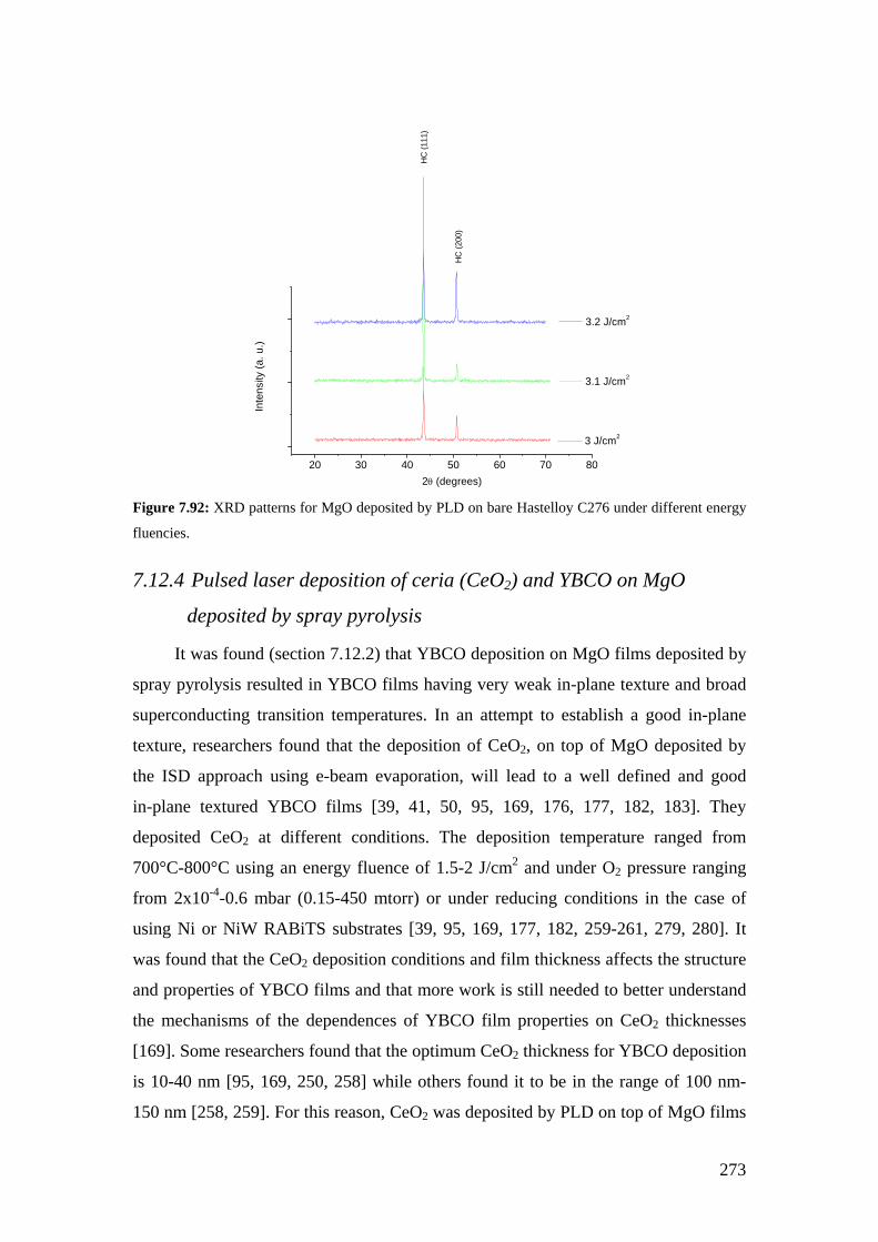
273
20 30 40 50 60 70 80
3.2 J/cm2
3.1 J/cm2
3 J/cm2 H
C (2
00)
HC
(111
)
Inte
nsity
(a. u
.)
2θ (degrees) Figure 7.92: XRD patterns for MgO deposited by PLD on bare Hastelloy C276 under different energy
fluencies.
7.12.4 Pulsed laser deposition of ceria (CeO2) and YBCO on MgO
deposited by spray pyrolysis
It was found (section 7.12.2) that YBCO deposition on MgO films deposited by
spray pyrolysis resulted in YBCO films having very weak in-plane texture and broad
superconducting transition temperatures. In an attempt to establish a good in-plane
texture, researchers found that the deposition of CeO2, on top of MgO deposited by
the ISD approach using e-beam evaporation, will lead to a well defined and good
in-plane textured YBCO films [39, 41, 50, 95, 169, 176, 177, 182, 183]. They
deposited CeO2 at different conditions. The deposition temperature ranged from
700°C-800°C using an energy fluence of 1.5-2 J/cm2 and under O2 pressure ranging
from 2x10⁻⁴-0.6 mbar (0.15-450 mtorr) or under reducing conditions in the case of
using Ni or NiW RABiTS substrates [39, 95, 169, 177, 182, 259-261, 279, 280]. It
was found that the CeO2 deposition conditions and film thickness affects the structure
and properties of YBCO films and that more work is still needed to better understand
the mechanisms of the dependences of YBCO film properties on CeO2 thicknesses
[169]. Some researchers found that the optimum CeO2 thickness for YBCO deposition
is 10-40 nm [95, 169, 250, 258] while others found it to be in the range of 100 nm-
150 nm [258, 259]. For this reason, CeO2 was deposited by PLD on top of MgO films

274
deposited by spray pyrolysis followed by YBCO deposition by PLD as well in an
attempt to improve the texture and superconducting properties of YBCO.
CeO2 has a cubic (fluorite, CaF2) structure with a lattice constant at room
temperature of 5.411Å with a cation coordination number of 8. In CaF2 calcium ions
are positioned at the centers of cubes, with fluorine ions at the corners. One unit cell
consists of eight cubes, as indicated in Figure 7.93. CeO2 is very stable even at very
high temperature. The large lattice mismatch between CeO2 and YBCO is reduced by
rotation of 45° in the CeO2 a-b lattice plane (in-plane). This way, the lattice mismatch
will be 0.16% and 1.7% along the a and b axis of YBCO, respectively. Besides that, it
is important to have (100) oriented CeO2 in order to grow c-axis oriented, epitaxial
YBCO films [70, 169, 184, 279, 281].
Figure 7.93: A unit cell for the fluorite crystal structure [70].
In this work CeO2 was deposited at two different conditions. The used energy
fluence was 2 J/cm2, the distance between the target and the substrate was fixed at
56 mm, 500 and 1000 pulses were applied as it was found by researchers that cracks
will form in 100-200nm thick CeO2 films [282-284]. The first deposition was made at
780°C using 0.6 mbar O2 and the second one was made at 710°C using 2x10⁻⁴ mbar
O2. The YBCO deposition conditions were the same as those mentioned in section
7.12.1. The depositions were made on the MgO films deposited by spray pyrolysis
from 0.468M solution at 650°C for 48 minutes.
The samples deposited with 500 pulses of CeO2 show very weak CeO2 peaks.
Therefore, the deposition proceeded from now on with only 1000 pulses. Figure 7.94

275
shows the XRD patterns for CeO2 films deposited on top of MgO films deposited by
spray pyrolysis. The CeO2 peaks were indexed according to the JCPDS PDF file 00-
004-0593 where the (111), (200), (220), and the (311) peaks occur at 2θs of 28.55°,
33.07°, 47.49°, and 56.32°, respectively. It can be seen that none of the CeO2
deposition conditions resulted in a perfectly (200) oriented films. However, the
deposition at 780°C using 0.6 mbar O2 resulted in a stronger CeO2 (200) peak
compared to the film deposited at 710°C using 2x10⁻⁴ mbar O2. The surface roughness
was increased after the CeO2 deposition as was clear from the SEM and AFM images
(Figure 7.95-Figure 7.98) compared to that before the deposition (Figure 7.24 and
Figure 7.29). The EDX test suggested that the formed particles were composed of Mg
and O with a ratio of Mg:O of 1:1.50.
20 30 40 50 60 70 80
CeO
2 (31
1)
CeO
2 (22
0)H
C (2
00)
HC
(111
)M
gO (2
00)
CeO
2 (20
0)
CeO
2 (11
1)
650oC 0.468M 48 min. Ceria 2x10⁻⁴mbar 710oC
650oC 0.468M 48 min. Ceria 0.6mbar 780oC
Inte
nsity
(a. u
.)
2θ (degrees)
Figure 7.94: XRD patterns for CeO2 films deposited by PLD at different conditions on the MgO films
spray pyrolysed at 650°C from 0.468M for 48 minutes.

276
Figure 7.95: SEM image for CeO2 film deposited by PLD at 710°C using 2x10⁻⁴ mbar O2 on the MgO
film deposited by spray pyrolysis at 650°C from 0.468M for 48 minutes.
Figure 7.96: SEM image for CeO2 film deposited by PLD at 780°C using 0.6 mbar O2 on the MgO
film deposited by spray pyrolysis at 650°C from 0.468M for 48 minutes.

277
Figure 7.97: A 5x5µm2 AFM image for CeO2 film deposited by PLD at 710°C using 2x10⁻⁴ mbar O2
on the MgO film spray pyrolysed at 650°C from 0.468M for 48 minutes.
Figure 7.98: A 5x5µm2 AFM image for CeO2 film deposited by PLD at 780°C using 0.6 mbar O2 on
the MgO film spray pyrolysed at 650°C from 0.468M for 48 minutes.
To see the influence of the deposited CeO2 film (even the surface was quite
rough) on the properties of the superconducting layer, YBCO was deposited on each

278
of the samples shown in Figure 7.94. Figure 7.99 shows the XRD patterns for YBCO
films deposited on CeO2. It is clear that the YBCO film had a stronger (006) peak on
the CeO2 film deposited at 780°C using 0.6 mbar O2. However, the YBCO films were
rougher as can be seen from the SEM images (Figure 7.100 and Figure 7.101) and
AFM images (Figure 7.102 and Figure 7.103), respectively, compared to the YBCO
film deposited directly on the MgO film deposited by spray pyrolysis (Figure 7.86 and
Figure 7.88). CeO2 film deposited at 780°C using 0.6 mbar resulted in smoother
YBCO film when compared to the CeO2 film deposited at 710°C using 2x10⁻⁴ mbar.
This can be attributed to the stronger CeO2 (200) peak deposited at 780°C using 0.6
mbar which gave a stronger YBCO (006) peak and hence smoother film. The cross
sectional SEM image in Figure 7.104 show that YBCO, CeO2 and MgO films had
thicknesses of about 1.384µm, 99nm and 342nm respectively. This means that the
deposition rate of YBCO was 13840 Å /5000 pulses = 2.7Å/pulse, and for CeO2
990Å/1000 pulses = 0.99Å/pulse and for MgO 3420 Å / (360sec) = 9.5Å/sec.
The pole figure in Figure 7.105 shows that YBCO has a good weak out-of-plane
texture but still no in-plane texture (no definite poles were obtained at the
circumference but a ring was obtained instead). This means that CeO2 deposition on
the MgO films deposited by spray pyrolysis had no effect in improving the in-plane
texture of the subsequent YBCO layer which disagrees with what was found by other
researchers [39, 41, 50, 95, 169, 176, 177, 182, 183]. In addition to that, both samples
shown in Figure 7.99 had no Tc.

279
0 10 20 30 40 50 60
650OC 0.468M 48 min Ceria 0.6mbar 780OC YBCO 0.6mbar 780OC
YBC
O (0
07)
650OC 0.468M 48 min Ceria 2X10⁻⁴mbar 710OC YBCO 0.6mbar 780OC
HC
(111
)YB
CO
(006
)H
C (1
11)
MgO
(200
)YB
CO
(005
)
YBC
O (0
13)
YBC
O (0
04)
CeO
2 (2
00)
CeO
2 (1
11)
YBC
O (0
03)
YBC
O (0
02)
YBC
O (0
01)
Inte
nsity
(a. u
.)
2θ (degrees) Figure 7.99: XRD patterns for YBCO and CeO2 films deposited by PLD at different conditions on the
MgO films spray pyrolysed at 650°C from 0.468M for 48 minutes.
Figure 7.100: SEM image for YBCO on CeO2 film deposited by PLD at 710°C using 2x10⁻⁴ mbar O2
on the MgO film spray pyrolysed at 650°C from 0.468M for 48 minutes.
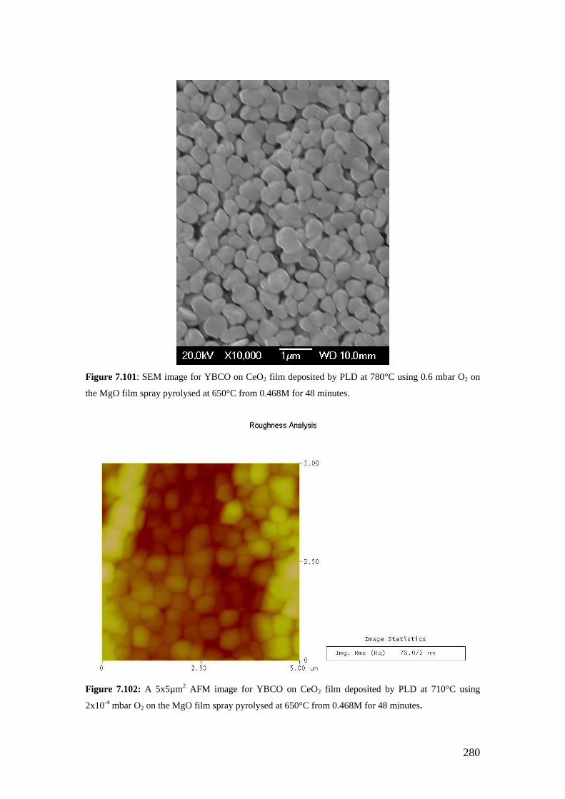
280
Figure 7.101: SEM image for YBCO on CeO2 film deposited by PLD at 780°C using 0.6 mbar O2 on
the MgO film spray pyrolysed at 650°C from 0.468M for 48 minutes.
Figure 7.102: A 5x5µm2 AFM image for YBCO on CeO2 film deposited by PLD at 710°C using
2x10⁻⁴ mbar O2 on the MgO film spray pyrolysed at 650°C from 0.468M for 48 minutes.

281
Figure 7.103: A 5x5µm2 AFM image for YBCO on CeO2 film deposited by PLD at 780°C using 0.6
mbar O2 on the MgO film spray pyrolysed at 650°C from 0.468M for 48 minutes.
Figure 7.104: Cross sectional SEM image for YBCO on CeO2 film deposited by PLD at 780°C using
0.6 mbar O2 on the MgO film spray pyrolysed at 650°C from 0.468M for 48 minutes.
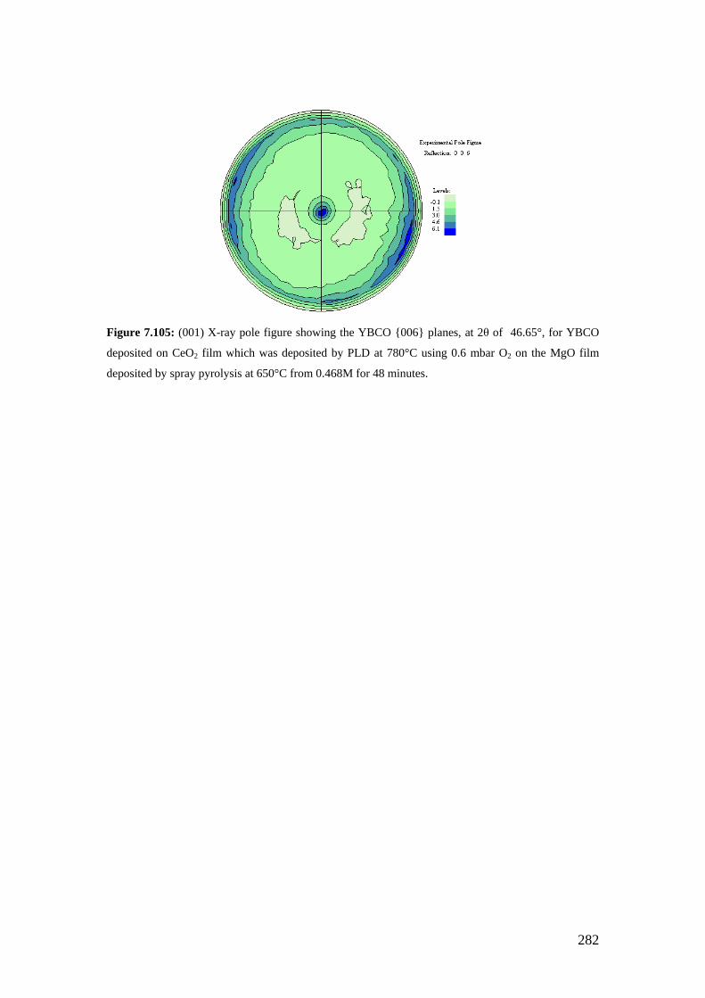
282
Figure 7.105: (001) X-ray pole figure showing the YBCO {006} planes, at 2θ of 46.65°, for YBCO
deposited on CeO2 film which was deposited by PLD at 780°C using 0.6 mbar O2 on the MgO film
deposited by spray pyrolysis at 650°C from 0.468M for 48 minutes.

283
8 Spray pyrolysis of MgO on Hastelloy C276 from
acetate precursor
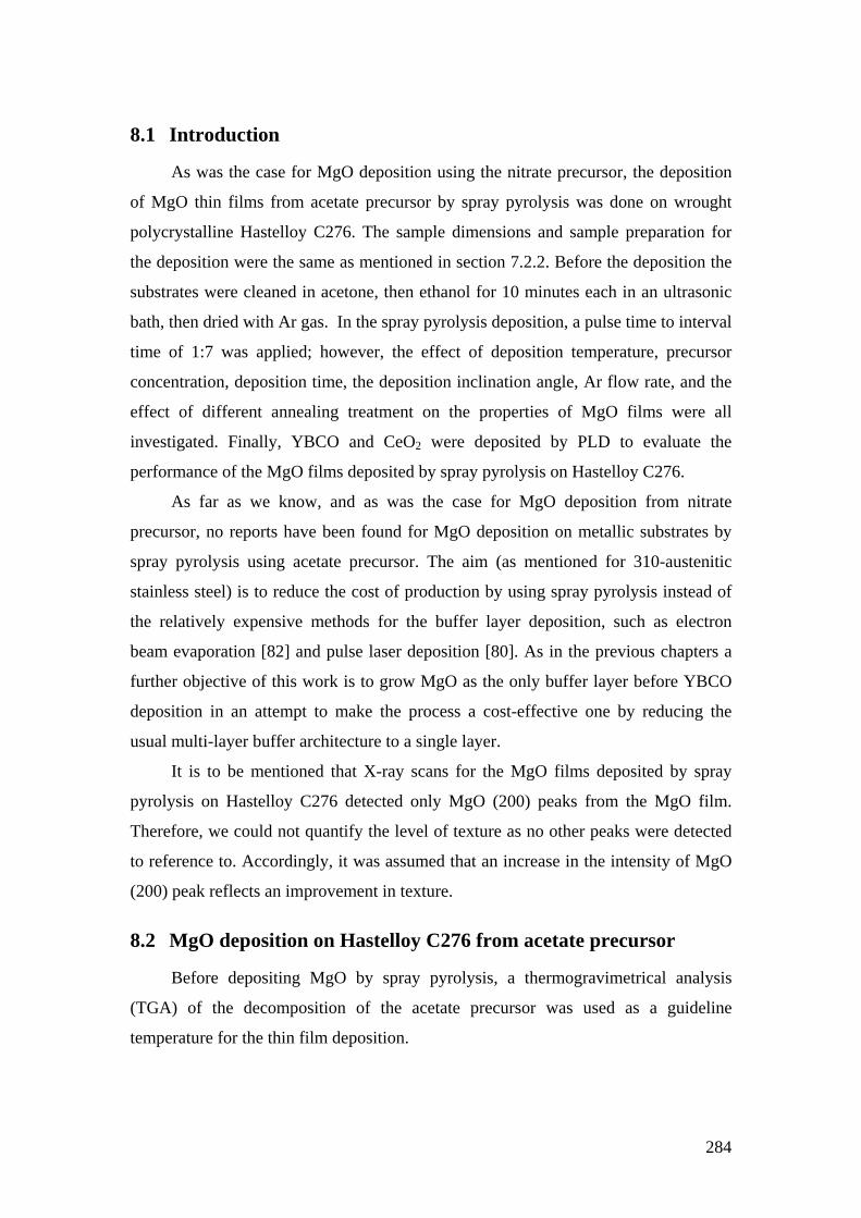
284
8.1 Introduction
As was the case for MgO deposition using the nitrate precursor, the deposition
of MgO thin films from acetate precursor by spray pyrolysis was done on wrought
polycrystalline Hastelloy C276. The sample dimensions and sample preparation for
the deposition were the same as mentioned in section 7.2.2. Before the deposition the
substrates were cleaned in acetone, then ethanol for 10 minutes each in an ultrasonic
bath, then dried with Ar gas. In the spray pyrolysis deposition, a pulse time to interval
time of 1:7 was applied; however, the effect of deposition temperature, precursor
concentration, deposition time, the deposition inclination angle, Ar flow rate, and the
effect of different annealing treatment on the properties of MgO films were all
investigated. Finally, YBCO and CeO2 were deposited by PLD to evaluate the
performance of the MgO films deposited by spray pyrolysis on Hastelloy C276.
As far as we know, and as was the case for MgO deposition from nitrate
precursor, no reports have been found for MgO deposition on metallic substrates by
spray pyrolysis using acetate precursor. The aim (as mentioned for 310-austenitic
stainless steel) is to reduce the cost of production by using spray pyrolysis instead of
the relatively expensive methods for the buffer layer deposition, such as electron
beam evaporation [82] and pulse laser deposition [80]. As in the previous chapters a
further objective of this work is to grow MgO as the only buffer layer before YBCO
deposition in an attempt to make the process a cost-effective one by reducing the
usual multi-layer buffer architecture to a single layer.
It is to be mentioned that X-ray scans for the MgO films deposited by spray
pyrolysis on Hastelloy C276 detected only MgO (200) peaks from the MgO film.
Therefore, we could not quantify the level of texture as no other peaks were detected
to reference to. Accordingly, it was assumed that an increase in the intensity of MgO
(200) peak reflects an improvement in texture.
8.2 MgO deposition on Hastelloy C276 from acetate precursor
Before depositing MgO by spray pyrolysis, a thermogravimetrical analysis
(TGA) of the decomposition of the acetate precursor was used as a guideline
temperature for the thin film deposition.
285
8.2.1 Thermal decomposition of the acetate precursor
A sample of magnesium acetate, Mg(CH3COO)2.4H2O, with a mass of 7 mg
was placed in an alumina crucible. The thermogravimetric (TGA) analysis was
performed in a flow of Argon from 25°C to 750°C. The TGA measurement was
performed at a constant heating rate of 10°C/min. Figure 8.1 shows the TGA curve for
the tested Mg(CH3COO)2.4H2O sample.
0 100 200 300 400 500 600 700 800
30
40
50
60
70
80
90
100
110
TG (
wei
ght l
oss
%)
Temperature (oC)
Figure 8.1: TG curve for Mg(CH3COO)2.4H2O.
The decomposition of magnesium acetate takes place in three steps according to
the following equations [285]:
Mg(CH3COO)2.4H2O Mg(CH3COO)2 + 4H2O (Eq. 8.1)
Mg(CH3COO)2 MgCO3 + (CH3)2.CO (acetone) (g) (Eq. 8.2)
MgCO3 MgO + CO2 (g) (Eq. 8.3)
Dehydration occurs in the first step. The decomposition of the acetates proceeds
in the next two steps, by the release of acetone and CO2 to yield MgO. It can be seen
from Figure 8.1 that the decomposition finished at about 400οC and beyond about
450°C no weight loss takes place, suggesting the formation of stoichiometric MgO.
Similar results were obtained by A. Moses et al and McAdie et al [285, 286].
Therefore, the deposition of MgO was done at temperatures higher than 450°C.
286
8.3 Effect of deposition temperature on MgO film properties
Magnesium acetate [Mg(CH3COO)2.4H2O] as a precursor was used to deposit
MgO by spray pyrolysis on Hastelloy C276 substrates. The deposition was done using
0.093M solution at different temperature for 32 minutes and using an Ar flow rate of
10 l/min. The XRD patterns after the deposition are shown in Figure 8.2 where MgO
(200) oriented XRD peaks were detected using a much lower concentration compared
to the nitrate precursor (Figure 7.22). The MgO peaks were indexed according to the
JCPDS PDF files 00-045-0946 where MgO (200) is at 2θ of 42.9°. As was the case
with the nitrate precursor, the MgO (200) peak, the only detected one, was normal to
the substrate surface. The thermal expansion coefficients of Hastelloy C276 and MgO
are 10.8-11.3x10⁻⁶ /°C and 13.8 x 10⁻⁶/°C, respectively [143, 267]. The lattice
parameter for MgO is 4.2112Å and for Hastelloy C276, as calculated from Bragg’s
law, is 3.5952Å and this gives a lattice mismatch of 17.1%. This explains the shift of
MgO peaks to 43.12°, however, this shift is not much compared to that obtained when
depositing MgO on Si single crystals. No MgO peaks were detected at 500°C,
although the EDX results (Figure 8.3 and Table 8.1) showed the presence of Mg,
therefore, the deposited MgO film was suggested to be amorphous. Figure 8.4 is the
SEM image for the sample deposited at 500°C. The intensity of the MgO (200) was
enhanced by increasing the temperature from 550°C to 600°C and to 650°C; however,
that was at the expense of the surface roughness as shown from the SEM images in
Figure 8.5-Figure 8.7 and Figure 8.8. Figure 8.9 is an AFM image for the MgO film
deposited at 550°C. The SEM images in Figure 8.4-Figure 8.6 show microstructures
which are very similar to the one obtained during MgO deposition on Si single crystal
from 0.078M solution at 650°C (Figure 4.5). This confirms that the microstructure of
the deposited MgO films depends on the substrate used; similar microstructures were
obtained on different substrates but by using different deposition temperatures and
different precursor. An AFM section profile image is shown in Figure 8.10 for MgO
film deposited from 0.093M solution at 550°C for 32 minutes. When comparing
Figure 8.5 and Figure 8.9 to Figure 8.10, it can be seen that the surface was
homogenous and smooth and most of the film was located on the same layer as can be
seen from Figure 8.10. The same was also observed for the film deposited from
0.093M solution at 500°C and 600°C. However, The MgO film deposited at 650°C
showed particles or grains which were located on different layers relative to the rest of

287
the film. According to the deposition modes of spray pyrolysis [83], the smooth
surfaces for the films deposited at 500°C, 550°C and 600°C (Figure 8.4-Figure 8.6)
were consistent with the third mode of deposition; when thermal decomposition of dry
precipitates starts on their way to the substrate. However, at 500°C, the temperature
was not high enough to form textured MgO films. The film deposited at 650°C
(Figure 8.7) which showed higher roughness due to the formation of particles on the
surface was deposited according to the fourth mode of deposition; where the full
thermal decomposition takes place before reaching the substrate and only finely
divided solid products arrive at the substrate surface.
The EDX results for the films deposited at 550°C-650°C suggest that the
deposited MgO was almost stoichiometric with a ratio of Mg:O very close to 1:1 as
can be seen from Figure 8.11 and Table 8.2 for the MgO film deposited at 600°C from
0.093M solution for 32 minutes.
42 44 46 48 50 52
500οC 0.093M
650οC 0.093M
600οC 0.093M
550οC 0.093M
MgO
(200
)
HC
(200
)
HC
(111
)
Inte
nsity
(a. u
.)
2θ (degrees) Figure 8.2: XRD patterns for MgO deposition on Hastelloy C276 using 0.093M of
Mg(CH3COO)2.4H2O at different temperatures for 32 minutes.

288
Figure 8.3: EDX spectrum, using an accelerating voltage of 4KV, for MgO with 0.093M at 500°C with
a deposition time of 32 minutes.
Table 8.1: Summary of the EDX chemical composition results, using an accelerating voltage of 4KV,
for MgO with 0.093M at 500°C with a deposition time of 32 minutes.
Element at %
O K 30.42
Mg K 18.97
Cr L 10.00
Fe L 3.66
Ni L 30.84
W M 0.77
Mo L 5.34

289
Figure 8.4: SEM image for the MgO film deposited on Hastelloy C276 using 0.093M of
Mg(CH3COO)2.4H2O at 500°C for 32 minutes.
Figure 8.5: SEM image for the MgO film deposited on Hastelloy C276 using 0.093M of
Mg(CH3COO)2.4H2O at 550°C for 32 minutes.

290
Figure 8.6: SEM image for the MgO film deposited on Hastelloy C276 using 0.093M of
Mg(CH3COO)2.4H2O at 600°C for 32 minutes.
Figure 8.7: SEM image for the MgO film deposited on Hastelloy C276 using 0.093M of
Mg(CH3COO)2.4H2O at 650°C for 32 minutes.
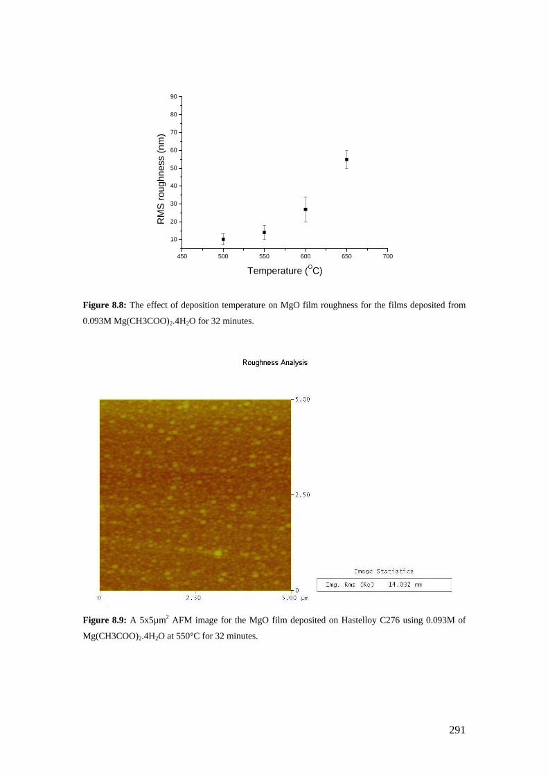
291
450 500 550 600 650 700
10
20
30
40
50
60
70
80
90
RM
S ro
ughn
ess
(nm
)
Temperature (OC)
Figure 8.8: The effect of deposition temperature on MgO film roughness for the films deposited from
0.093M Mg(CH3COO)2.4H2O for 32 minutes.
Figure 8.9: A 5x5µm2 AFM image for the MgO film deposited on Hastelloy C276 using 0.093M of
Mg(CH3COO)2.4H2O at 550°C for 32 minutes.

292
Figure 8.10: AFM section profile image for the MgO film deposited on Hastelloy C276 using 0.093M
of Mg(CH3COO)2.4H2O at 550°C for 32 minutes.
MgO
1 2 3 4 5 6 7 8 9 10keVFull Scale 5186 cts Cursor: 0.000
Spectrum 1
Figure 8.11: EDX spectrum, using an accelerating voltage of 4KV, for MgO film deposited with
0.093M solution at 600°C for a deposition time of 32 minutes.
Table 8.2: Summary of the EDX chemical composition results, using an accelerating voltage of 4KV,
for MgO film deposited with 0.093M solution at 600°C for a deposition time of 32 minutes.
Element at %
O K 52.06
Mg K 47.94
The texture of MgO was stronger (Figure 8.2) compared to that obtained when
using the nitrate precursor (Figure 7.22 and Figure 7.34). This was also confirmed

293
from the X-ray pole figure measurements for the samples deposited at 600°C and
650°C for 32 minutes from 0.093M solution (Figure 8.12 and Figure 8.13,
respectively). It can be seen that there is a weak out-of-plane texture and no in-plane
texture (no definite poles were obtained at the circumference but a ring was obtained
instead) as was the case for the nitrate precursor. The out-of-plane texture of MgO
(200) was quantitatively measured by the ω-scan for the sample deposited at 600°C
(Figure 8.14) and 650°C (Figure 8.16) from 0.093M solution. The FWHM for MgO
(200) was 18.7° and 17.67°, respectively.
Figure 8.12: (200) X-ray pole figure, at 2θ of 43.12°, of the MgO film deposited at 600°C from a
solution of 0.093M for 32 minutes.
Figure 8.13: (200) X-ray pole figure, at 2θ of 43.12°, of the MgO film deposited at 650°C from a
solution of 0.093M for 32 minutes.
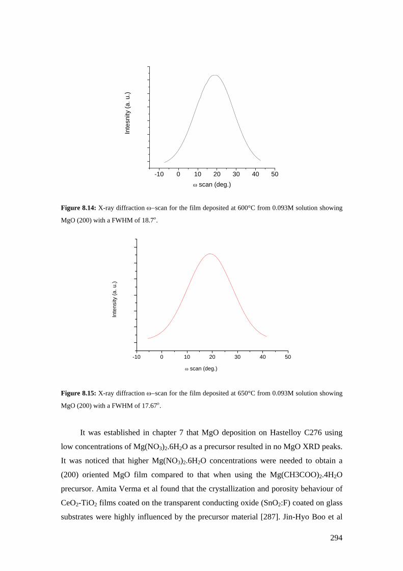
294
-10 0 10 20 30 40 50
Inte
snity
(a. u
.)
ω scan (deg.)
Figure 8.14: X-ray diffraction ω−scan for the film deposited at 600°C from 0.093M solution showing
MgO (200) with a FWHM of 18.7ο.
-10 0 10 20 30 40 50
Inte
nsity
(a. u
.)
ω scan (deg.)
Figure 8.15: X-ray diffraction ω−scan for the film deposited at 650°C from 0.093M solution showing
MgO (200) with a FWHM of 17.67ο.
It was established in chapter 7 that MgO deposition on Hastelloy C276 using
low concentrations of Mg(NO3)2.6H2O as a precursor resulted in no MgO XRD peaks.
It was noticed that higher Mg(NO3)2.6H2O concentrations were needed to obtain a
(200) oriented MgO film compared to that when using the Mg(CH3COO)2.4H2O
precursor. Amita Verma et al found that the crystallization and porosity behaviour of
CeO2-TiO2 films coated on the transparent conducting oxide (SnO2:F) coated on glass
substrates were highly influenced by the precursor material [287]. Jin-Hyo Boo et al

295
found that the type of the precursor will affect the crystallinity, in terms of the
preferred orientation, of MgO films deposited by metal-organic chemical vapour
deposition (MOCVD) on c-plane sapphire substrates [288]. Soo Gil Kim et al found
that the (100) preferred orientation of the MgO thin film deposited on Corning 7059
glass substrates was not affected by the type of the solvent used [289]. O. Renault and
M. Labeau [146] deposited MgO on glass substrates using aerosol
assisted-metalorganic chemical vapour deposition. They found that the deposition rate
and the texture of MgO films changed by changing the nature of the solvent and that
the deposition rate increased with increasing the deposition temperature. They
concluded that the nature of the solvent and the aerosol flow rate both may play an
important role on the obtained microstructure, as they control, in a way that is not
fully understood yet, the deposition rate and processes at a given substrate
temperature, and hence the direction of texture. So it can be seen that the solvent type
and the precursor may or may not affect the preferred orientation of the produced
film. In this study, it is still not clear why higher concentrations of the
Mg(NO3)2.6H2O precursor was required for the deposition of MgO on Hastelloy C276
and more investigation is required in this field. However, it was believed that under
the deposition conditions used during spray pyrolysis and the way the
Mg(NO3)2.6H2O decomposes, a high vapour pressure of the Mg2+ cation was obtained
when using low precursor concentration, hence, high number of collisions which in
turn leads to its deficiency in the film. That is why higher concentrations were needed.
8.4 Effect of deposition time on MgO film properties
The effect of the deposition time on the deposited MgO films by spray pyrolysis
was studied at different temperatures, using an Ar flow rate of 10 l/min, as can be
seen from the XRD patterns in Figure 8.16. It can be seen that regardless of the
deposition temperature, the intensity of MgO (200) increased by increasing the
deposition time from 32 minutes to 64 minutes. However, the increase in intensity
was accompanied by an increase in the roughness. This can be noticed by comparing
the SEM images (Figure 8.17 and Figure 8.18) and the AFM images (Figure 8.19 and
Figure 8.20) for the samples with a deposition time of 64 minutes with those with a
deposition time of 32 minutes (Figure 8.5, Figure 8.6 and Figure 8.8).
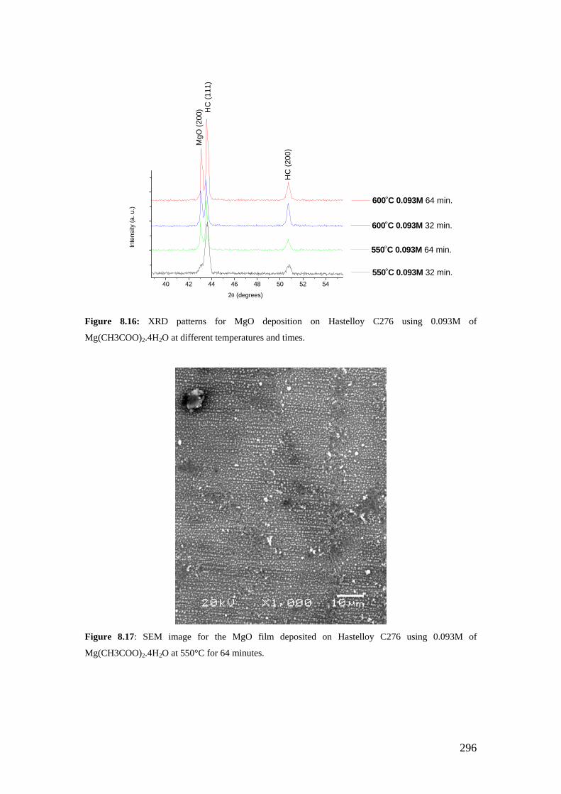
296
40 42 44 46 48 50 52 54
MgO
(200
) HC
(111
)
HC
(200
)
Inte
nsity
(a. u
.)
2θ (degrees)
550οC 0.093M 32 min.
550οC 0.093M 64 min.
600οC 0.093M 32 min.
600οC 0.093M 64 min.
Figure 8.16: XRD patterns for MgO deposition on Hastelloy C276 using 0.093M of
Mg(CH3COO)2.4H2O at different temperatures and times.
Figure 8.17: SEM image for the MgO film deposited on Hastelloy C276 using 0.093M of
Mg(CH3COO)2.4H2O at 550°C for 64 minutes.

297
Figure 8.18: SEM image for the MgO film deposited on Hastelloy C276 using 0.093M of
Mg(CH3COO)2.4H2O at 600°C for 64 minutes.
Figure 8.19: A 5x5µm2 AFM image for the MgO film deposited on Hastelloy C276 using 0.093M of
Mg(CH3COO)2.4H2O at 550°C for 64 minutes.

298
Figure 8.20: A 5x5µm2 AFM image for the MgO film deposited on Hastelloy C276 using 0.093M of
Mg(CH3COO)2.4H2O at 600°C for 64 minutes.
The fourth mode of deposition leads to the formation of particles on the surface
by increasing the temperature, where the full thermal decomposition takes place
before the substrate and only finely divided solid product arrives at the substrate
surface. It is also to be pointed out that the actual working mode depends not only on
the substrate temperature, but also on the temperature of the working surrounding
[83]. By increasing the deposition time from 32 minutes to 64 minutes, overgrown
particles were formed suggesting that the growth of the particles is dominating the
nucleation. However, no sound explanation was found to relate this behaviour with
the type of the deposition mode that might be applied to this situation and further
investigation is required.
In an attempt to improve the texture of the MgO (200) peak, without increasing
the roughness, a double deposition was made. This means that the sample was
deposited at certain conditions, left to be furnace cooled to room temperature, then
deposited again at the same conditions. This was done at 600°C for 32 minutes each
using 0.093M solution.
The XRD patterns in
Figure 8.21 show that the intensity of the MgO peak was not improved much.
This slight improvement in intensity was accompanied by a slight increase in the

299
roughness as can be seen from the SEM images and AFM image in Figure 8.22 and
Figure 8.23, respectively, when compared to the sample without the double deposition
(Figure 8.6 and Figure 8.8). If it is assumed that the thickness of MgO film increases
with increasing the deposition time, then it can be concluded that the texture improved
slightly with thickness. Similar behaviour was found by other researchers [142, 146,
175]. More details on thickness dependence are found in section 8.7.
42 44 46 48 50 52 54
600οC 0.093M 32 minutes Double deposition
600οC 0.093M 32 minutes
MgO
(200
)
HC
(200
)
HC
(111
)
Inte
nsity
(a. u
.)
2θ (degrees)
Figure 8.21: XRD patterns for MgO deposition on Hastelloy C276 showing the double deposition
effect using 0.093M Mg(CH3COO)2.4H2O at 600°C for 32 minutes.

300
Figure 8.22: SEM image for MgO on Hastelloy C276 with the double deposition using 0.093M
Mg(CH3COO)2.4H2O at 600°C for 32 minutes.
Figure 8.23: A 5x5µm2 AFM image for MgO on Hastelloy C276 with the double deposition using
0.093M Mg(CH3COO)2.4H2O at 600°C for 32 minutes.

301
8.5 Effect of precursor concentration on MgO film properties
MgO deposition on Hastelloy C276 was done at higher concentrations, using
0.14M and 0.279M solutions at 600°C, and using an Ar flow rate of 10 l/min. As can
be seen from the XRD patterns in Figure 8.24, an MgO (200) peak, the only detected
one, was normal to the substrate surface. It can also be seen that the peak intensity
was not greatly affected by increasing the concentration. This can be attributed to the
saturation effect; at concentrations higher than 0.093M, the growth rate will be low
and hence the film thickness will not increase significantly, therefore almost no effect
on texture was obtained. C. H. Lee and C. S. Huang [158] deposited In2O3 by spray
pyrolysis on Si wafers using InCl3-methanol solution as the source material, they
found that at high flow rates, the growth rate is slow due to the reactant saturation
effect. Other researchers [86] found that, for MgO films deposited on Si (100)
substrates by electrostatic spray pyrolysis, the growth rate decreased with increasing
the substrate temperature, others [114] found that, for ZnO films deposited on glass
substrates by spray pyrolysis, at high temperatures the deposition rate was constant
(saturated) where the growth rate is mass transport controlled; the reaction kinetics are
so fast that the surface reaction finally becomes controlled by mass transfer of the
reactants, and the concentration of the reactants on the surface is the limiting
parameter.
When using the 0.14M solution, the roughness increased quite slightly as can be
seen from the SEM image (Figure 8.25) and the AFM image (Figure 8.27) compared
to that when using the 0.093M solution (Figure 8.6 and Figure 8.8); however, there
was a further increase in the roughness when increasing the concentration to 0.279M
as can be seen from the SEM image (Figure 8.26) and the AFM image (Figure 8.28),
respectively. At 0.279M, overgrown particles were formed on the surface which led to
an increase in the roughness. The lifetime required for evaporation increases by
increasing the amount of solute in the droplet [110]; therefore, by increasing the
concentration to 0.279M, the time was not enough to evaporate both the solvent and
the solute, a situation similar to that encountered in the second mode of deposition
[83]. A similar behaviour was encountered when depositing MgO from the nitrate
precursor using 0.78M (Figure 7.27).

302
42 44 46 48 50 52 54
600οC 0.140M 32 minutes
600οC 0.279M 32 minutes
600οC 0.093M 32 minutes
MgO
(200
)
HC
(200
)
HC
(111
)
Inte
nsity
(a. u
.)
2θ (degrees)
Figure 8.24: XRD patterns for MgO deposition on Hastelloy C276 at 600°C for 32 minutes using
different concentrations of Mg(CH3COO)2.4H2O.
Figure 8.25: SEM image for MgO deposition on Hastelloy C276 at 600°C for 32 minutes using 0.14M
Mg(CH3COO)2.4H2O.

303
Figure 8.26: SEM image for MgO deposition on Hastelloy C276 at 600°C for 32 minutes using
0.279M Mg(CH3COO)2.4H2O.
Figure 8.27: A 5x5µm2 AFM image for MgO deposition on Hastelloy C276 at 600°C for 32 minutes
using 0.14M Mg(CH3COO)2.4H2O.

304
Figure 8.28: A 5x5µm2 AFM image for MgO deposition on Hastelloy C276 at 600°C for 32 minutes
using 0.279M Mg(CH3COO)2.4H2O.
When using the nitrate precursor, the low concentration (0.078M) resulted in
amorphous MgO films. Higher concentrations were needed (0.468M and 0.78M) to
get a weak MgO (200) peak. In contrast, the use of the acetate precursor resulted in
textured MgO films even when using low concentrations (0.093M). This would be
attributed to the nature of the used precursor, where it was established from the
literature that the solvent type and the precursor may or may not affect the preferred
orientation of the produced film (section 8.3). Therefore, in this study, the type of the
precursor, and this time the type of the substrate as well, affects the concentration
needed to get textured MgO films.
8.6 X-ray photoelectron spectroscopy (XPS) test
The samples deposited from 0.093M at 550°C and 600°C for 32 minutes using
10 l/min Ar flow rate were tested for surface contamination using the XPS. The XPS
spectra were recorded with a standard Mg Kα source using 20 pass energy, 0.1 eV
step, and 0.1 seconds per step for the detailed spectra. The Mg 2P scan was from 40-
60eV and the O 1s scan was from 520-550eV. For the sample deposited at 550°C, the
Mg 2P was found to be at 49.8eV (Figure 8.29). For the O 1s two peaks were obtained

305
at 529.8eV and at 531.5eV (Figure 8.30). For the sample deposited at 600°C, the
Mg 2P was found to be at 50.5eV (Figure 8.31). For and the O 1s two peaks were also
obtained at 531.3eV and at 532.9eV (Figure 8.32). The peak position for Mg 2P is due
to the contribution of magnesium oxide/hydroxide (Figure 8.29 and Figure 8.31). In
the O 1s spectra (Figure 8.30 and Figure 8.32), the two peak positions are for
magnesium oxide and magnesium hydroxide. This indicates that the surface of MgO
was contaminated with hydroxides as was expected as MgO is hygroscopic [194].
Similar result was found by others [201-208]. However, heating the contaminated
layer briefly at a temperature of 450°C in air is sufficient to regenerate the MgO
surface [116]; in our experiments this condition will be met during subsequent YBCO
deposition. Although the sample analysis was carried out on fresh samples to
minimise the effect of storage.
40 45 50 55 60
Mg source40-60eV0.1eV step, 0.1 sec. dwell 20 E pass
Mg 2P eV=49.8 (oxide and hydroxide)
Inte
nsity
(a. u
.)
Binding Energy (a. u.)
Figure 8.29: XPS spectrum for the MgO thin film deposited on Hastelloy C276 substrate using
0.093M Mg(CH3COO)2.4H2O at 550οC for 32 min. showing the Mg 2P.

306
525 530 535
Mg source520-550eV0.1eV step, 0.1 sec. dwell 20 E pass
O 1S eV=531.5 (hydroxide)
O 1S eV=529.8 (oxide)
Inte
nsity
(a. u
.)
Binding Energy (eV)
Figure 8.30: XPS spectrum for the MgO thin film deposited on Hastelloy C276 substrate using
0.093M Mg(CH3COO)2.4H2O at 550οC for 32 min. showing the O 1S.
40 45 50 55 60
Mg 2P eV=50.5 (oxide and hydroxide)
Mg source40-60eV0.1eV step, 0.1 sec. dwell 20 E pass
Inte
nsity
(a. u
.)
Binding Energy (eV)
Figure 8.31: XPS spectrum for the MgO thin film deposited on Hastelloy C276 substrate using
0.093M Mg(CH3COO)2.4H2O at 600οC for 32 min. showing the Mg 2P.
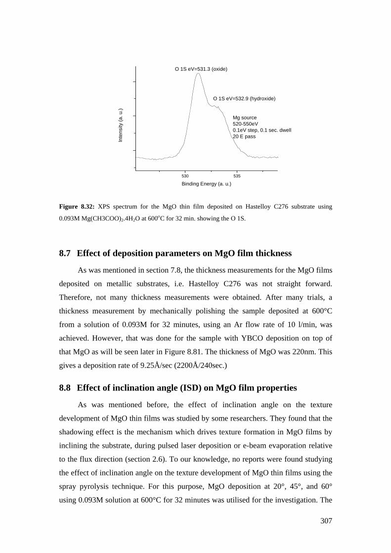
307
530 535
O 1S eV=532.9 (hydroxide)
O 1S eV=531.3 (oxide)
Mg source520-550eV0.1eV step, 0.1 sec. dwell 20 E pass
Inte
nsity
(a. u
.)
Binding Energy (a. u.)
Figure 8.32: XPS spectrum for the MgO thin film deposited on Hastelloy C276 substrate using
0.093M Mg(CH3COO)2.4H2O at 600οC for 32 min. showing the O 1S.
8.7 Effect of deposition parameters on MgO film thickness
As was mentioned in section 7.8, the thickness measurements for the MgO films
deposited on metallic substrates, i.e. Hastelloy C276 was not straight forward.
Therefore, not many thickness measurements were obtained. After many trials, a
thickness measurement by mechanically polishing the sample deposited at 600°C
from a solution of 0.093M for 32 minutes, using an Ar flow rate of 10 l/min, was
achieved. However, that was done for the sample with YBCO deposition on top of
that MgO as will be seen later in Figure 8.81. The thickness of MgO was 220nm. This
gives a deposition rate of 9.25Å/sec (2200Å/240sec.)
8.8 Effect of inclination angle (ISD) on MgO film properties
As was mentioned before, the effect of inclination angle on the texture
development of MgO thin films was studied by some researchers. They found that the
shadowing effect is the mechanism which drives texture formation in MgO films by
inclining the substrate, during pulsed laser deposition or e-beam evaporation relative
to the flux direction (section 2.6). To our knowledge, no reports were found studying
the effect of inclination angle on the texture development of MgO thin films using the
spray pyrolysis technique. For this purpose, MgO deposition at 20°, 45°, and 60°
using 0.093M solution at 600°C for 32 minutes was utilised for the investigation. The
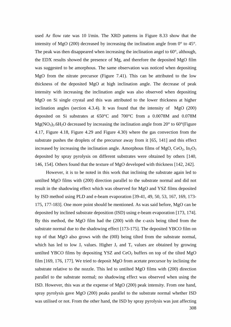
308
used Ar flow rate was 10 l/min. The XRD patterns in Figure 8.33 show that the
intensity of MgO (200) decreased by increasing the inclination angle from 0° to 45°.
The peak was then disappeared when increasing the inclination angel to 60°, although,
the EDX results showed the presence of Mg, and therefore the deposited MgO film
was suggested to be amorphous. The same observation was noticed when depositing
MgO from the nitrate precursor (Figure 7.41). This can be attributed to the low
thickness of the deposited MgO at high inclination angle. The decrease of peak
intensity with increasing the inclination angle was also observed when depositing
MgO on Si single crystal and this was attributed to the lower thickness at higher
inclination angles (section 4.3.4). It was found that the intensity of MgO (200)
deposited on Si substrates at 650°C and 700°C from a 0.0078M and 0.078M
Mg(NO3)2.6H2O decreased by increasing the inclination angle from 20° to 60°(Figure
4.17, Figure 4.18, Figure 4.29 and Figure 4.30) where the gas convection from the
substrate pushes the droplets of the precursor away from it [65, 141] and this effect
increased by increasing the inclination angle. Amorphous films of MgO, CeO2, In2O3
deposited by spray pyrolysis on different substrates were obtained by others [140,
146, 154]. Others found that the texture of MgO developed with thickness [142, 242].
However, it is to be noted in this work that inclining the substrate again led to
untilted MgO films with (200) direction parallel to the substrate normal and did not
result in the shadowing effect which was observed for MgO and YSZ films deposited
by ISD method using PLD and e-beam evaporation [39-41, 49, 50, 53, 167, 169, 173-
175, 177-183]. One more point should be mentioned. As was said before, MgO can be
deposited by inclined substrate deposition (ISD) using e-beam evaporation [173, 174].
By this method, the MgO film had the (200) with the c-axis being tilted from the
substrate normal due to the shadowing effect [173-175]. The deposited YBCO film on
top of that MgO also grows with the (00l) being tilted from the substrate normal,
which has led to low Jc values. Higher Jc and Tc values are obtained by growing
untilted YBCO films by depositing YSZ and CeO2 buffers on top of the tilted MgO
film [169, 176, 177]. We tried to deposit MgO from acetate precursor by inclining the
substrate relative to the nozzle. This led to untilted MgO films with (200) direction
parallel to the substrate normal; no shadowing effect was observed when using the
ISD. However, this was at the expense of MgO (200) peak intensity. From one hand,
spray pyrolysis gave MgO (200) peaks parallel to the substrate normal whether ISD
was utilised or not. From the other hand, the ISD by spray pyrolysis was just affecting

309
the crystallinity (Figure 8.33), roughness (Figure 8.34) and thickness of the deposited
MgO films. YBCO films grown on top of MgO deposited by spray pyrolysis (as will
be seen later in this chapter) have the (006) of YBCO // (200) of MgO. Thus, spray
pyrolysis offers an alternative method of depositing a single MgO buffer layer with no
tilting for later YBCO deposition. The same behaviour was also observed for MgO
deposition from the nitrate precursor.
42 45 48 51 54 600οC 0.093M 0O
600οC 0.093M 60O
600οC 0.093M 45O
600οC 0.093M 20O
MgO
(200
)
HC
(200
)HC
(111
)
Inte
nsity
(a. u
.)
2θ (degrees) Figure 8.33: XRD patterns for MgO deposition on Hastelloy C276 using 0.093M
Mg(CH3COO)2.4H2O at 600°C for 32 minutes and at different inclination angles.
Figure 8.34-Figure 8.37 show that the roughness decreased with increasing the
inclination angel from 20° to 60°, similar behaviour was found for MgO deposition on
Si single crystals (Figure 4.31). This behaviour can be attributed to pushing of
droplets of the precursor away from the substrates, and by increasing the inclination
angle, smoother films were obtained. However, for MgO deposition on Si, the RMS
of the film deposited with no inclination angle was rougher than the ones deposited
with an inclination angle. A different situation was encountered when depositing
MgO on Hastelloy C276. At zero inclination angle, the surface roughness was about
27 nm, and by increasing the inclination angle to 20°, the surface roughness increased
to about 33 nm then decreased by increasing the inclination angle to 45° and 60°. This
increase in the roughness at 20° may be attributed to a flow turbulence at the substrate
surface leading to the formation of particles and hence to an increase in the roughness.
This turbulence decreased by increasing the inclination angle, and therefore to a
decrease in the roughness values. This behaviour was not really understood and

310
further investigation is required. The same behaviour was observed for MgO
deposition from the nitrate precursor (Figure 7.42). Rachel E. Koritala et al [185]
found that for the case of biaxially textured MgO films deposited by ISD using
e-beam evaporation on Hastelloy C substrates that high roughness values were
obtained at low and high inclination angles and the lowest roughness values were
obtained for inclination angles of 20°-55° where the roughness was not affected by
the inclination angle in this range.
0 10 20 30 40 50 60 700
10
20
30
40
50
60
RM
S ro
ughn
ess
(nm
)
Inclination angle (degrees)
Figure 8.34: The effect of inclination angle on the film roughness of MgO film deposited from 0.093M
solution at 600°C for 32 minutes.
Figure 8.35: SEM image for MgO deposition on Hastelloy C276 using 0.093M Mg(CH3COO)2.4H2O
at 600°C for 32 minutes at 20°.
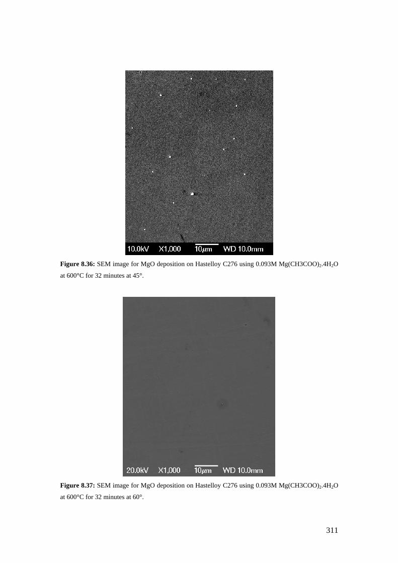
311
Figure 8.36: SEM image for MgO deposition on Hastelloy C276 using 0.093M Mg(CH3COO)2.4H2O
at 600°C for 32 minutes at 45°.
Figure 8.37: SEM image for MgO deposition on Hastelloy C276 using 0.093M Mg(CH3COO)2.4H2O
at 600°C for 32 minutes at 60°.
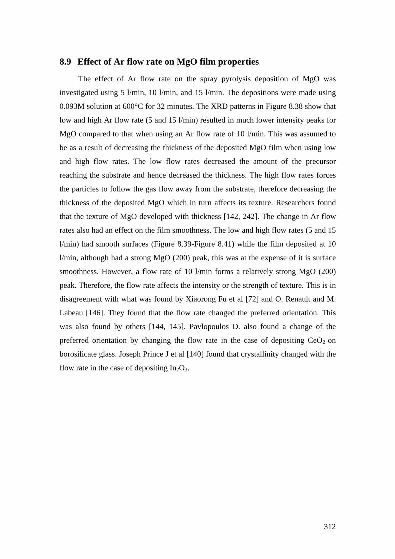
312
8.9 Effect of Ar flow rate on MgO film properties
The effect of Ar flow rate on the spray pyrolysis deposition of MgO was
investigated using 5 l/min, 10 l/min, and 15 l/min. The depositions were made using
0.093M solution at 600°C for 32 minutes. The XRD patterns in Figure 8.38 show that
low and high Ar flow rate (5 and 15 l/min) resulted in much lower intensity peaks for
MgO compared to that when using an Ar flow rate of 10 l/min. This was assumed to
be as a result of decreasing the thickness of the deposited MgO film when using low
and high flow rates. The low flow rates decreased the amount of the precursor
reaching the substrate and hence decreased the thickness. The high flow rates forces
the particles to follow the gas flow away from the substrate, therefore decreasing the
thickness of the deposited MgO which in turn affects its texture. Researchers found
that the texture of MgO developed with thickness [142, 242]. The change in Ar flow
rates also had an effect on the film smoothness. The low and high flow rates (5 and 15
l/min) had smooth surfaces (Figure 8.39-Figure 8.41) while the film deposited at 10
l/min, although had a strong MgO (200) peak, this was at the expense of it is surface
smoothness. However, a flow rate of 10 l/min forms a relatively strong MgO (200)
peak. Therefore, the flow rate affects the intensity or the strength of texture. This is in
disagreement with what was found by Xiaorong Fu et al [72] and O. Renault and M.
Labeau [146]. They found that the flow rate changed the preferred orientation. This
was also found by others [144, 145]. Pavlopoulos D. also found a change of the
preferred orientation by changing the flow rate in the case of depositing CeO2 on
borosilicate glass. Joseph Prince J et al [140] found that crystallinity changed with the
flow rate in the case of depositing In2O3.
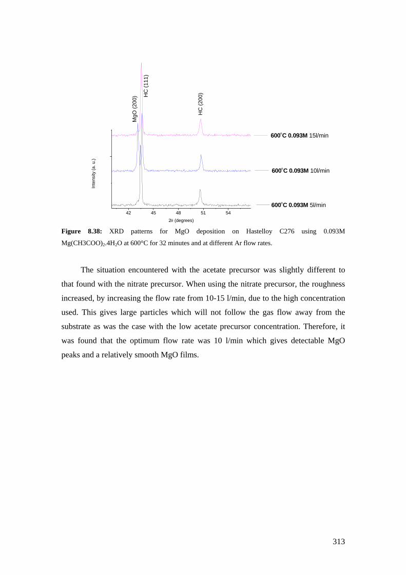
313
42 45 48 51 54
600οC 0.093M 15l/min
600οC 0.093M 10l/min
600οC 0.093M 5l/min
MgO
(200
)
HC
(200
)HC
(111
)
Inte
nsity
(a. u
.)
2θ (degrees) Figure 8.38: XRD patterns for MgO deposition on Hastelloy C276 using 0.093M
Mg(CH3COO)2.4H2O at 600°C for 32 minutes and at different Ar flow rates.
The situation encountered with the acetate precursor was slightly different to
that found with the nitrate precursor. When using the nitrate precursor, the roughness
increased, by increasing the flow rate from 10-15 l/min, due to the high concentration
used. This gives large particles which will not follow the gas flow away from the
substrate as was the case with the low acetate precursor concentration. Therefore, it
was found that the optimum flow rate was 10 l/min which gives detectable MgO
peaks and a relatively smooth MgO films.

314
Figure 8.39: SEM image for the Hastelloy C276 deposited with MgO using 0.093M solution at 600°C
for 32 minutes and using an Ar flow rate of 5 l/min.
Figure 8.40: SEM image for the Hastelloy C276 deposited with MgO using 0.093M solution at 600°C
for 32 minutes and using an Ar flow rate of 15 l/min.
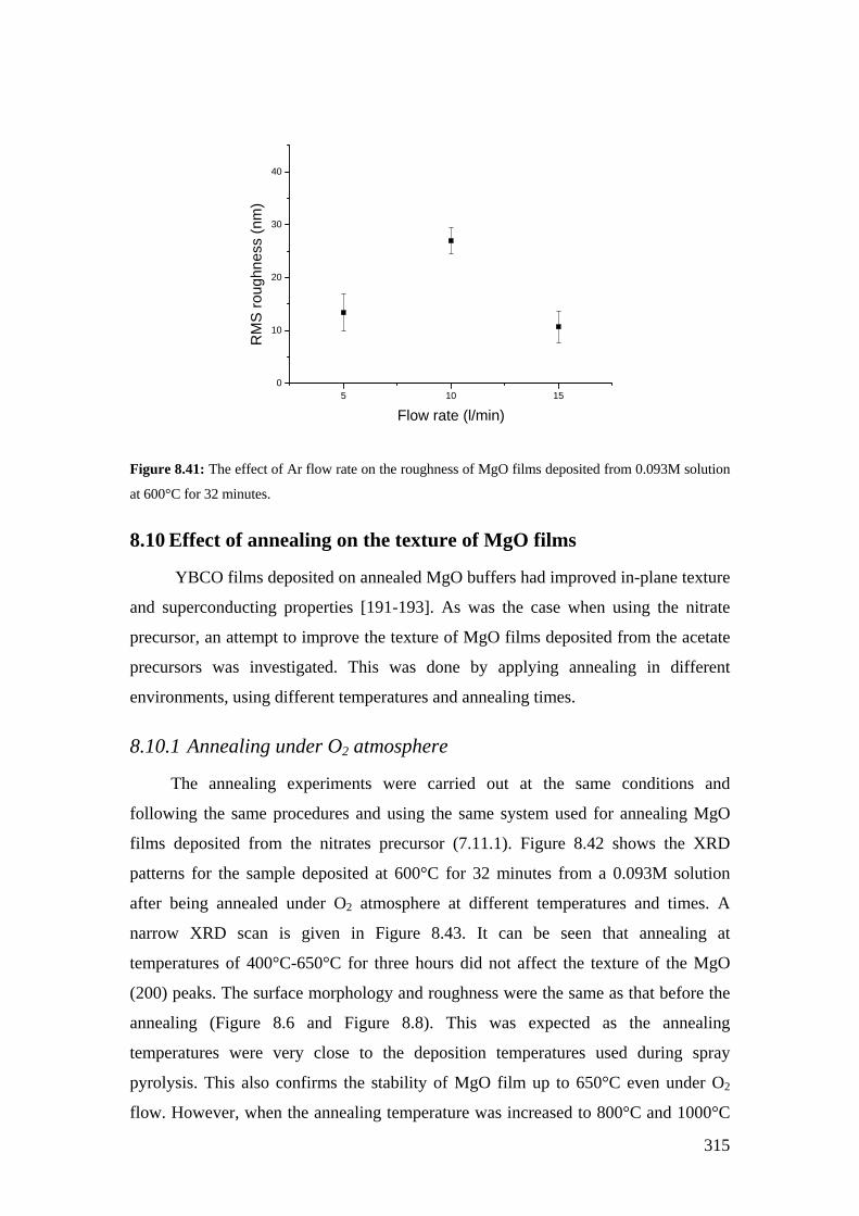
315
5 10 150
10
20
30
40
RM
S ro
ughn
ess
(nm
)
Flow rate (l/min)
Figure 8.41: The effect of Ar flow rate on the roughness of MgO films deposited from 0.093M solution
at 600°C for 32 minutes.
8.10 Effect of annealing on the texture of MgO films
YBCO films deposited on annealed MgO buffers had improved in-plane texture
and superconducting properties [191-193]. As was the case when using the nitrate
precursor, an attempt to improve the texture of MgO films deposited from the acetate
precursors was investigated. This was done by applying annealing in different
environments, using different temperatures and annealing times.
8.10.1 Annealing under O2 atmosphere
The annealing experiments were carried out at the same conditions and
following the same procedures and using the same system used for annealing MgO
films deposited from the nitrates precursor ( 7.11.1). Figure 8.42 shows the XRD
patterns for the sample deposited at 600°C for 32 minutes from a 0.093M solution
after being annealed under O2 atmosphere at different temperatures and times. A
narrow XRD scan is given in Figure 8.43. It can be seen that annealing at
temperatures of 400°C-650°C for three hours did not affect the texture of the MgO
(200) peaks. The surface morphology and roughness were the same as that before the
annealing (Figure 8.6 and Figure 8.8). This was expected as the annealing
temperatures were very close to the deposition temperatures used during spray
pyrolysis. This also confirms the stability of MgO film up to 650°C even under O2
flow. However, when the annealing temperature was increased to 800°C and 1000°C

316
for a deposition time of three hours, other oxides started to appear (Figure 8.42), even
a powder film of oxides formed on the surface, which is why the MgO (200) peak
disappeared. The oxides were more pronounced by annealing at 1000°C for three
hours. The oxide peaks could not be indexed and were referred to as complex oxides.
It was believed that such oxides were composed of Ni and Cr in a complex chemistry
which was why no JCPDS PDF files were found to index them.
20 30 40 50 60 70 80
* complex oxides* * * * *
600oC 0.093M
MgO
(200
)H
C (1
11)
HC
(200
)
600oC 0.093M 1000oC O2 3hrs
600oC 0.093M 400oC O2 3hrs
600oC 0.093M 600oC O2 3hrs
600oC 0.093M 650oC O2 3hrs
600oC 0.093M 800oC O2 3hrs
Inte
nsity
(a. u
.)
2θ (degrees) Figure 8.42: XRD patterns for the Hastelloy substrates deposited with MgO from 0.093M at 600°C for
32 minutes after O2 anneal at different temperatures and times.
42 44 46 48 50 52
** complex oxides
*
600oC 0.093M
MgO
(200
) HC
(111
)
HC
(200
)
600oC 0.093M 1000oC O2 3hrs
600oC 0.093M 400oC O2 3hrs
600oC 0.093M 600oC O2 3hrs
600oC 0.093M 650oC O2 3hrs
600oC 0.093M 800oC O2 3hrs
Inte
nsity
(a. u
.)
2θ (degrees) Figure 8.43: XRD patterns with a narrow scan for the Hastelloy substrates deposited with MgO from
0.093M at 600°C for 32 minutes after O2 anneal at different temperatures and times.
The SEM and AFM images for the samples annealed at 800°C and 1000°C for
three hours are shown in Figure 8.44-Figure 8.47. At 800°C, grain boundaries of the

317
substrate were revealed due to the thermal etching (Figure 8.44) and not due to any
sensitisation effects. As from the boiling acid test it was found that the substrates were
not susceptible to sensitisation. The revealing of the grain boundaries at high
temperatures was even seen during pulsed laser deposition of YBCO on NiW
RABiTS by Y L Cheung et al [259, 261]. The thermal etching effect on Ni RABiTS
was also seen by others [32, 264, 265]. Therefore, grain boundaries were revealed as a
result of thermal etching and this was also confirmed by heating a bare Hastelloy
substrate at 800°C under O2 atmosphere for three hours, where the same grain
boundary structure was observed (Figure 8.48).
For MgO films, it can be seen that the surface roughness increased by
annealing. It was 27 nm for the sample before annealing (Figure 8.8) and became 60
nm (as an average of three readings) for the sample annealed at 800°C for three hours
and 240 nm (as an average of three readings) for the sample annealed at 1000°C for
three hours. The EDX test showed an increase in the Cr and Ni content in addition to
very low percentage of Mg, and this can be used to suggest the presence of complex
oxides and the disappearance of the MgO (200) peak.
From this, it is clear that annealing up to 650°C was not improving the texture
nor deteriorating the MgO film. However, annealing at 800°C-1000°C affected the
surface stability by the oxidation of the substrate.

318
Figure 8.44: SEM image for the Hastelloy substrate deposited with MgO at 600°C for 32 minutes from
0.093M solution then annealed at 800°C under O2 for three hours.
Figure 8.45: SEM image for the Hastelloy substrate deposited with MgO at 600°C for 32 minutes from
0.093M solution then annealed at 1000°C under O2 for three hours.
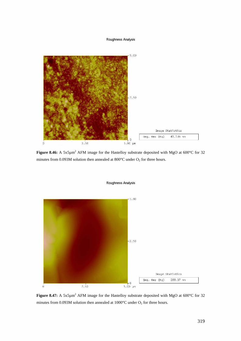
319
Figure 8.46: A 5x5µm2 AFM image for the Hastelloy substrate deposited with MgO at 600°C for 32
minutes from 0.093M solution then annealed at 800°C under O2 for three hours.
Figure 8.47: A 5x5µm2 AFM image for the Hastelloy substrate deposited with MgO at 600°C for 32
minutes from 0.093M solution then annealed at 1000°C under O2 for three hours.
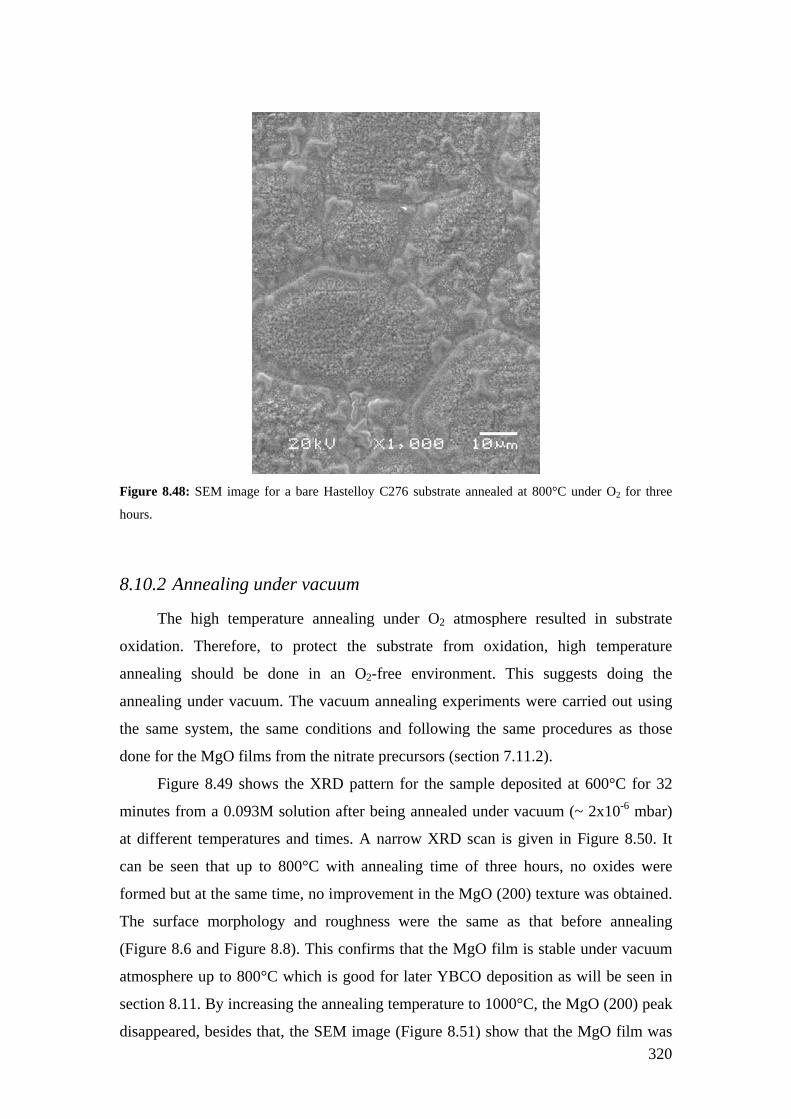
320
Figure 8.48: SEM image for a bare Hastelloy C276 substrate annealed at 800°C under O2 for three
hours.
8.10.2 Annealing under vacuum
The high temperature annealing under O2 atmosphere resulted in substrate
oxidation. Therefore, to protect the substrate from oxidation, high temperature
annealing should be done in an O2-free environment. This suggests doing the
annealing under vacuum. The vacuum annealing experiments were carried out using
the same system, the same conditions and following the same procedures as those
done for the MgO films from the nitrate precursors (section 7.11.2).
Figure 8.49 shows the XRD pattern for the sample deposited at 600°C for 32
minutes from a 0.093M solution after being annealed under vacuum (~ 2x10⁻⁶ mbar)
at different temperatures and times. A narrow XRD scan is given in Figure 8.50. It
can be seen that up to 800°C with annealing time of three hours, no oxides were
formed but at the same time, no improvement in the MgO (200) texture was obtained.
The surface morphology and roughness were the same as that before annealing
(Figure 8.6 and Figure 8.8). This confirms that the MgO film is stable under vacuum
atmosphere up to 800°C which is good for later YBCO deposition as will be seen in
section 8.11. By increasing the annealing temperature to 1000°C, the MgO (200) peak
disappeared, besides that, the SEM image (Figure 8.51) show that the MgO film was

321
severely affected and grain boundaries were revealed on the substrate as a result of
thermal etching. The EDX test showed Mg deficiency (Figure 8.52 and Table 8.3).
This deficiency was due to Mg evaporation as was the case with the nitrate precursor
(Figure 7.61) and confirmed when annealing MgO single crystals at the same
conditions (Table 7.7 and Table 7.8). This behaviour was not mentioned by
researchers who applied annealing treatments on MgO substrates [191-193].
However, some groups found that annealing MgB2 resulted in Mg evaporation. K. A.
Yates et al found that annealing MgB2 (in vacuum) at 500°C resulted in significant
Mg loss [277]. Z. Y. Fan et al [278] found that the onset of significant Mg evaporation
under vacuum (10-9 torr) was observed near 425°C. The surface roughness of the
sample increased from 27 nm before annealing (Figure 8.8) to about 50 nm after
annealing (Figure 8.53). This increase in roughness was due to the high annealing
temperature. This may enhance diffusion processes to occur in the MgO film leading
to the formation of a rough surface.
20 30 40 50 60 70
MgO
(200
)H
C (1
11)
HC
(200
)
600oC 0.093M
600oC 0.093M 650oC Vac. 3hrs
600oC 0.093M 800oC Vac. 3hrs
600oC 0.093M 1000oC Vac. 3hrs
Inte
nsity
(a. u
.)
2θ (degrees) Figure 8.49: XRD patterns for the Hastelloy substrate deposited with MgO from 0.093M at 600°C for
32 minutes after vacuum anneal at different temperatures and times.
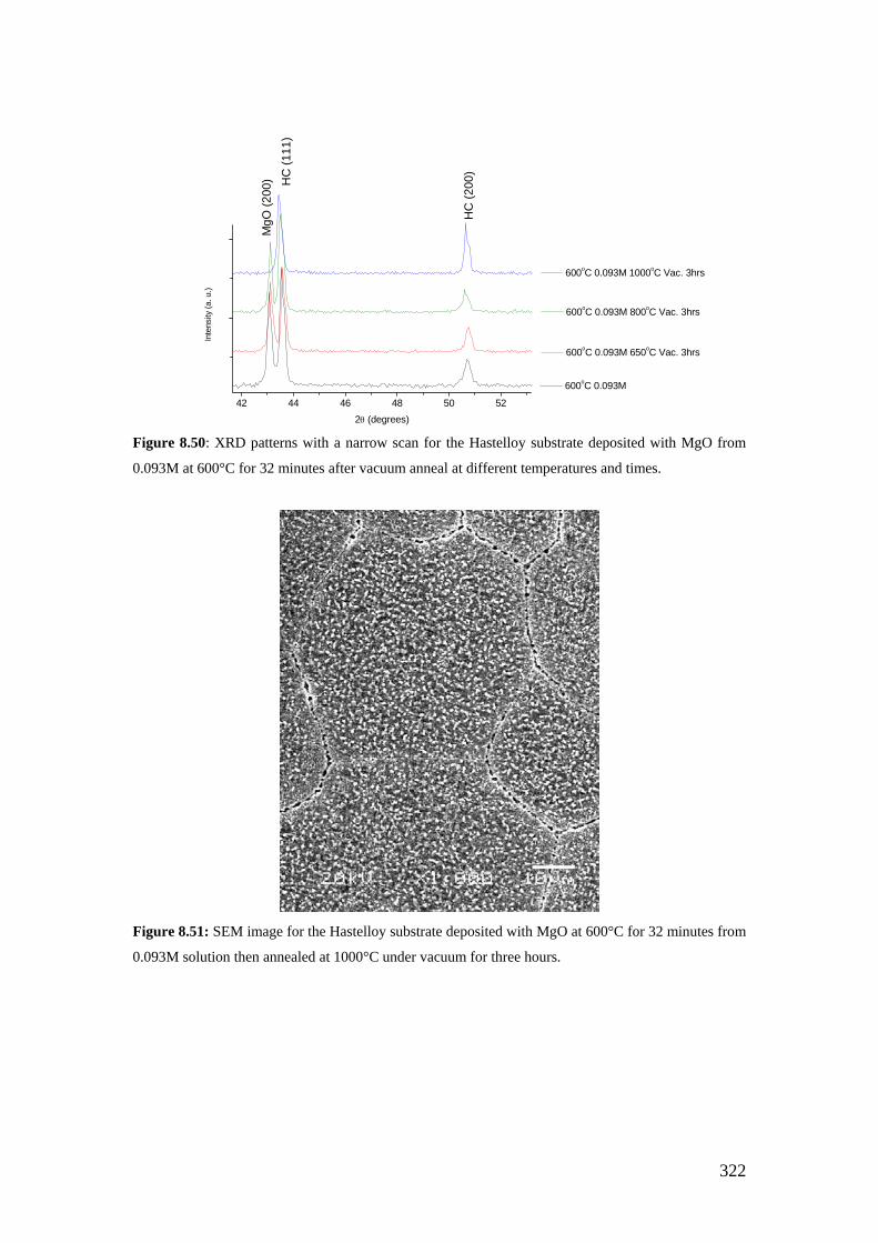
322
42 44 46 48 50 52
MgO
(200
) HC
(111
)
HC
(200
)
600oC 0.093M
600oC 0.093M 650oC Vac. 3hrs
600oC 0.093M 800oC Vac. 3hrs
600oC 0.093M 1000oC Vac. 3hrs
Inte
nsity
(a. u
.)
2θ (degrees) Figure 8.50: XRD patterns with a narrow scan for the Hastelloy substrate deposited with MgO from
0.093M at 600°C for 32 minutes after vacuum anneal at different temperatures and times.
Figure 8.51: SEM image for the Hastelloy substrate deposited with MgO at 600°C for 32 minutes from
0.093M solution then annealed at 1000°C under vacuum for three hours.

323
MoWMoW
W Mo
MgNi
CrO
0.5 1 1.5 2 2.5 3 3.5 4 4.5 5 5.5 6 6.5 7 7.5 8keVFull Scale 3835 cts Cursor: 0.332 (86 cts)
Spectrum 1
Figure 8.52: EDX spectrum, using an accelerating voltage of 4KV, for MgO film deposited on
Hastelloy C276 using 0.093M at 600°C with a deposition time of 32 minutes after being annealed at
1000°C for 3 hours.
Table 8.3: Summary of the EDX chemical composition results, using an accelerating voltage of 4KV,
for MgO film deposited on Hastelloy C276 using 0.093M at 600°C with a deposition time of 32
minutes after being annealed at 1000°C for 3 hours.
Element at %
O K 42.87
Mg K 17.81
Cr L 11.79
Ni L 15.35
Mo L 10.71
W M 1.47

324
Figure 8.53: A 5x5µm2 AFM image for the Hastelloy substrate deposited with MgO at 600°C for 32
minutes from 0.093M solution then annealed at 1000°C under vacuum for three hours.
In order to confirm that Mg evaporation needs high vacuum and high
temperature to evaporate, we conducted a high temperature anneal using purified Ar.
After pumping the system to 3.75x10⁻⁷ torr, 0.25 bar (0.246 atm.) of purified Ar was
purged to the system. The purification was made to get rid of any traces of oxygen or
moisture that may be present in Ar. After that, the sample was heated to 1000°C at a
rate of 300°C/hr and held at that temperature for three hours then the sample was
furnace cooled.
The XRD patterns in Figure 8.54 show that the annealing under purified Ar, for
the sample deposited from 0.093M solution at 600C for 32 minutes, did not result in
the elimination of the MgO (200) as a result of Mg evaporation as occurred during
vacuum anneal (Figure 8.50), however, the peak intensity was slightly lower
compared to that before Ar anneal. This confirms that the high temperature of
annealing should be combined with high vacuum to lead to significant Mg
evaporation. The SEM image for the sample after Ar annealing is shown in Figure
8.55. The AFM showed an RMS value of 45 nm compared to 27 nm for the sample
before annealing (Figure 8.6 and Figure 8.8). This may be attributed to the high

325
temperature anneal which enhanced diffusion processes leading to the formation of
tiny particles which in turn contribute to the deterioration of the surface smoothness.
42 44 46 48 50 52 54 56
MgO
(200
)H
C (1
11)
HC
(200
)
600oC 0.093M
600oC 0.093M 1000oC Ar 3hrs
Inte
nsity
(a. u
.)
2θ (degrees) Figure 8.54: XRD patterns for the Hastelloy substrate deposited with MgO from 0.093M solution at
600°C for 32 minutes then annealed under 0.25 bar purified Ar at 1000°C for three hours.
Figure 8.55: SEM image for the Hastelloy substrate deposited with MgO from 0.093M solution at
600°C for 32 minutes then annealed under 0.25 bar purified Ar at 1000C for three hours.

326
8.11 YBCO and ceria (CeO2) deposition by PLD
8.11.1 Introduction
As in the previous chapters an objective of this work is to grow MgO as the
only buffer layer before YBCO deposition in an attempt to make the process a
cost-effective one by reducing the usual multi-layer buffer architecture to a single
layer. To evaluate the performance of the MgO as a buffer the YBCO films have been
deposited by PLD. This is a well established route to high quality films [244, 245],
although spray pyrolysis of the YBCO layer should also be a possibility in the future
[23, 24, 87, 93, 94]. YBCO deposition parameters were the same as those mentioned
in section 7.12.1.
8.11.2 YBCO deposition on MgO spray pyrolysed at different
temperatures, precursor concentrations and deposition times.
Before YBCO deposition, the MgO films deposited from 0.093M at 550°C and
600°C were heated in the YBCO deposition chamber at the same conditions used for
YBCO deposition to see the stability of MgO film. It was found that the intensity of
MgO (200) peak, surface morphology and surface smoothness were the same before
and after the heating. This confirmed the stability of MgO film during YBCO
deposition.
YBCO was deposited by PLD on MgO films spray pyrolysed at different
conditions. The MgO and YBCO peaks were indexed according to the JCPDS PDF
files 00-045-0946 and 00-038-1433, respectively. The XRD patterns in Figure 8.56
show that YBCO films deposited on MgO films deposited by spray pyrolysis from
0.093M solution at different deposition temperatures and times were polycrystalline.
The film deposited from 0.279M solution at 600°C for a deposition time for 32
minutes was polycrystalline as well. The SEM images (Figure 8.57-Figure 8.60) of
YBCO films deposited on MgO spray pyrolysed at the aforementioned conditions
showed a granular structure. The roughness of the deposited YBCO films (Figure
8.61-Figure 8.64) was found to be higher than the corresponding values of the MgO
buffers (Figure 8.19, Figure 8.20, Figure 8.8, and Figure 8.28, respectively).

327
0 10 20 30 40 50 60
600OC 0.279M 32 min.
650OC 0.093M 32 min.
600OC 0.093M 64 min.
550OC 0.093M 64 min.
YBC
O (1
16)
YBC
O (0
07)
HC
(200
)
YBC
O (0
06)
HC
(111
)M
gO (2
00)
YBC
O (1
13)
YBC
O (0
05)
YBC
O (1
03)
YBC
O (0
03)
YBC
O (0
02)
YBC
O (0
01)
Inte
nsity
(a. u
.)
2θ (degrees) Figure 8.56: XRD patterns for YBCO films deposited by PLD on the MgO films spray pyrolysed at
different conditions.
Figure 8.57: SEM image for YBCO film deposited on MgO film spray pyrolysed on Hastelloy C276
using 0.093M Mg(CH3COO)2.4H2O at 550°C for 64 minutes.
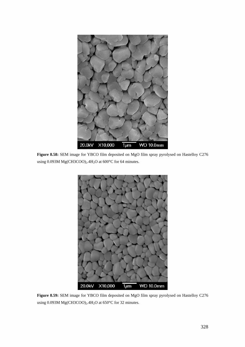
328
Figure 8.58: SEM image for YBCO film deposited on MgO film spray pyrolysed on Hastelloy C276
using 0.093M Mg(CH3COO)2.4H2O at 600°C for 64 minutes.
Figure 8.59: SEM image for YBCO film deposited on MgO film spray pyrolysed on Hastelloy C276
using 0.093M Mg(CH3COO)2.4H2O at 650°C for 32 minutes.

329
Figure 8.60: SEM image for YBCO film deposited on MgO film spray pyrolysed on Hastelloy C276
using 0.279M Mg(CH3COO)2.4H2O at 600°C for 32 minutes.
Figure 8.61: A 5x5µm2 AFM image for YBCO film deposited on MgO film spray pyrolysed on
Hastelloy C276 using 0.093M Mg(CH3COO)2.4H2O at 550°C for 64 minutes.

330
Figure 8.62: A 5x5µm2 AFM image for YBCO film deposited on MgO film spray pyrolysed on
Hastelloy C276 using 0.093M Mg(CH3COO)2.4H2O at 600°C for 64 minutes.
Figure 8.63: A 5x5µm2 AFM image for YBCO film deposited on MgO film spray pyrolysed on
Hastelloy C276 using 0.093M Mg(CH3COO)2.4H2O at 650°C for 32 minutes.

331
Figure 8.64: A 5x5µm2 AFM image for YBCO film deposited on MgO film spray pyrolysed on
Hastelloy C276 using 0.279M Mg(CH3COO)2.4H2O at 600°C for 32 minutes.
From the above, it was clear that the MgO films with RMS roughness greater
than about 42 nm (Figure 8.8, Figure 8.19, Figure 8.20, and Figure 8.28) resulted in
polycrystalline YBCO films (Figure 8.56). Only the smoothest MgO films (Figure
8.8, Figure 8.23, and Figure 8.27), i.e. the ones deposited at 600°C and 550°C using
0.093M for 32 minutes, and the ones deposited at 600°C using 0.093M for 32 minutes
with a double deposition, and at 600°C using 0.14M for 32 minutes, showed a well
textured YBCO films (Figure 8.65). However, a weak 103 peak was obtained and was
believed to be due to nucleation problems during the PLD deposition of YBCO. Such
peak was even seen for YBCO films deposited on MgO single crystals (Figure 4.57).
The (103) was lowest for the films deposited from 0.093M at 550°C and 600°C for 32
minutes. This demonstrates the critical role of the surface smoothness of MgO films,
deposited by spray pyrolysis from the acetate precursor, on the subsequent growth of
YBCO films as was the case for the nitrate precursor (section 7.12). The SEM images
for YBCO films show that the films were more continuous (Figure 8.66-Figure 8.69)
and smoother as can be seen from the AFM images in Figure 8.70-Figure 8.73,
compared to YBCO films deposited on spray pyrolysed MgO films under different
conditions (Figure 8.57-Figure 8.64). The film deposited at 550°C and 600°C from

332
0.093M solution for 32 minutes were found to be smoother (RMS 33 nm and 35nm,
respectively) compared to the films deposited at 600°C for 32 minutes using 0.093M
with a double deposition and 0.14M (RMS 60nm and 67, respectively). However,
pores were formed in all of the YBCO films. Such porous films were noticed by
others where it was attributed to the formation of Y2O3 or BaY2O4 [208, 209, 212].
The texture of MgO (200) was measured qualitatively using the X-ray pole figure
scans (Figure 8.12) and quantitatively using the X-ray ω-scans (Figure 8.14) for the
films deposited from 0.093M solution at 600°C for 32 minutes. From one hand, MgO
films deposited at 550°C and 600°C show the same weak out-of-plane and in-plane
texture. On the other hand, the YBCO films deposited on the MgO films spray
pyrolysed from 0.093M at 550°C and 600°C for 32 minutes had a better out-of-plane
texture (Figure 8.74 and Figure 8.75) with a FWHM of 12.5° and 11.6°, respectively
(Figure 8.76 and Figure 8.77, respectively). The improvement of YBCO out-of-plane
texture relative to the underlying buffers and substrate was observed by D. P. Norton
et al [257] where they found that the out-of-plane texture of YBCO was narrower than
the (100) Ni substrate and the CeO2 and YSZ buffers. This improvement resulted
from the low (001) surface energy and the anisotropic film growth nature commonly
observed for YBCO [290]. The in-plane texture for the films deposited at 550°C and
600°C was weak, however the film deposited at 600°C, show a kind of good in-plane
texture (Figure 8.75), although it was still weak and was confirmed by the phi scan in
Figure 8.78 which shows a FWHM of 40°. This implied that the texture of the
underlying MgO layer was copied by the growing YBCO film. It was also noticed that
both films i.e. the one deposited at 550°C and 600°C, had a good number of low angle
grain boundaries in addition to the presence of high angle grain boundaries (Figure
8.79 and Figure 8.80).
Figure 8.81 is a cross sectional SEM image for YBCO film deposited on MgO
spray pyrolysed at 600°C from 0.093M solution for 32 minutes. It can be seen that
YBCO, and MgO films had thicknesses of about 1.013 µm, 220 nm respectively. This
means that the deposition rate of YBCO was 10013/5000 = 2 Å/pulse, and for MgO
2200Å / (240sec) = 9.16 Å/sec which were close to that obtained for MgO deposition
from the nitrate precursor (section 7.8 and 7.12.4). The EDX scan suggested that the
YBCO film was nearly stoichiometric i.e. a ratio of Y:Ba:Cu was 1:2.06:3.2. An EDX
line scan across the substrate and the deposited MgO and YBCO films was performed
to see if MgO was a good barrier to diffusion or not (Figure 8.82). The figure shows

333
(as a weight %) that there was neither a diffusion of elements from the substrate to
YBCO film nor diffusion of YBCO elements to the substrate through the MgO buffer
layer and this confirmed that MgO functioned as a good diffusion barrier.
AC susceptibility at zero field showed a broad superconducting transition
temperature for all of the deposited YBCO films shown in Figure 8.65 with a Tc onset
of about 84.8K (Figure 8.83). From the AC curves it can be seen that the YBCO film
deposited on the spray pyrolysed MgO using 0.093M solution at 600°C for 32
minutes show a slightly better transition which can be attributed to a combination of
continuous, smoother and better texture of YBCO films deposited on such MgO films
compared to YBCO films deposited on the MgO films which were deposited under
the other spray pyrolysis conditions. YBCO films shown in Figure 8.56 had no Tc.
The effect of inclination angle, flow rate, annealing under O2, vacuum or Ar
atmospheres resulted either in rough surfaces or in decreasing the intensity of MgO
(200) peak. YBCO films deposited on such samples were polycrystalline and showed
no Tc.
It is to be noted in this work that inclining the substrate led to untilted MgO
films with (200) direction parallel to the substrate normal and did not result in the
shadowing effect which was observed for MgO and YSZ films deposited by ISD
method using PLD and e-beam evaporation [39-41, 49, 50, 53, 167, 169, 173-175,
177-183]. In this work, spray pyrolysis gave MgO (200) peaks parallel to the substrate
normal whether ISD was utilised or not. It was found by researchers that YBCO
deposition on c-axis tilted MgO resulted in c-axis tilted YBCO films. The tilt was
found to affect the superconducting properties, i.e. Jc and Tc [169, 176, 177]. In this
work YBCO films grown on top of the spray pyrolysed MgO films have the (006) of
YBCO // (200) of MgO. Thus, spray pyrolysis offers an alternative method of
depositing a single MgO buffer layer with no tilting for YBCO deposition.
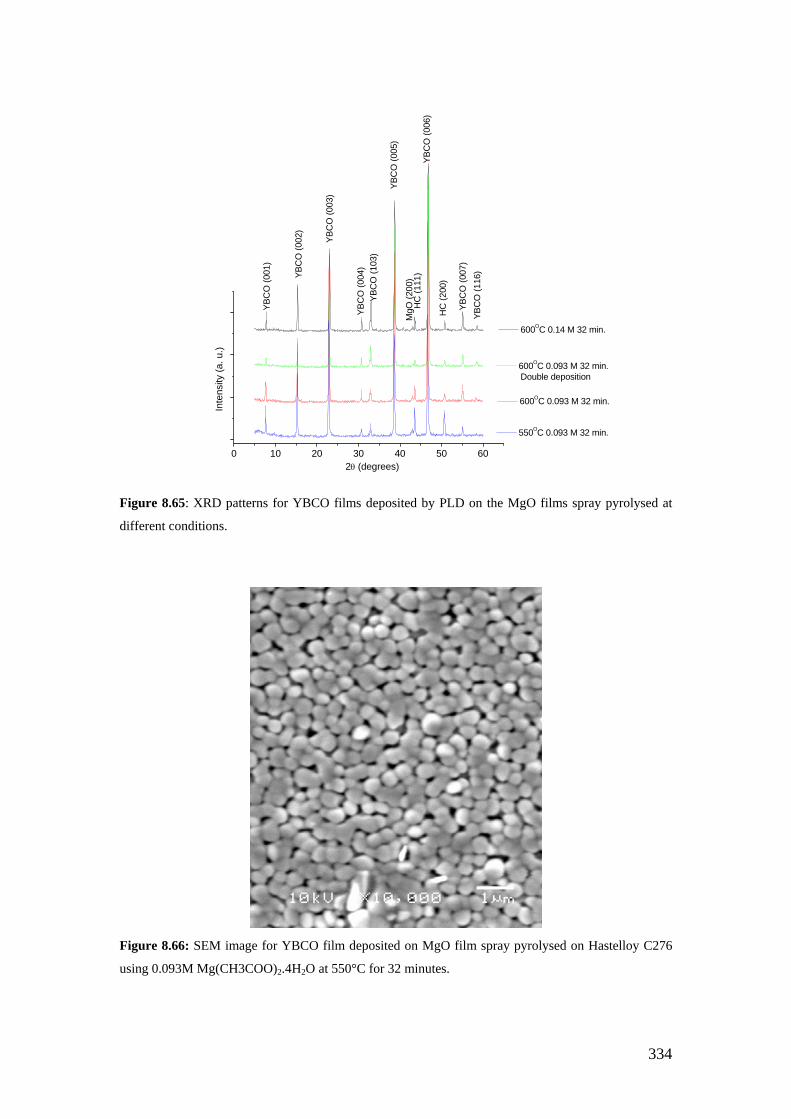
334
0 10 20 30 40 50 60
550OC 0.093 M 32 min.
600OC 0.093 M 32 min. Double deposition
600OC 0.14 M 32 min.
600OC 0.093 M 32 min.
YBC
O (1
16)
HC
(200
)
YBC
O (0
07)
YBC
O (0
06)
HC
(111
)M
gO (2
00)
YBC
O (0
05)
YBC
O (1
03)
YBC
O (0
04)
YBC
O (0
03)
YBC
O (0
02)
YBC
O (0
01)
Inte
nsity
(a. u
.)
2θ (degrees)
Figure 8.65: XRD patterns for YBCO films deposited by PLD on the MgO films spray pyrolysed at
different conditions.
Figure 8.66: SEM image for YBCO film deposited on MgO film spray pyrolysed on Hastelloy C276
using 0.093M Mg(CH3COO)2.4H2O at 550°C for 32 minutes.
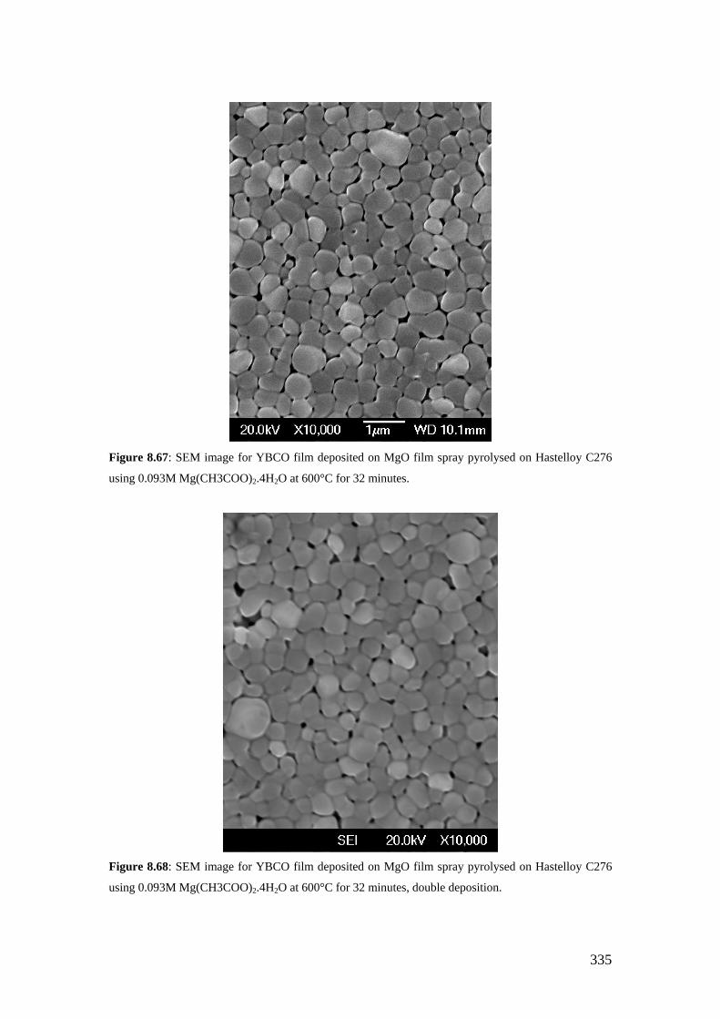
335
Figure 8.67: SEM image for YBCO film deposited on MgO film spray pyrolysed on Hastelloy C276
using 0.093M Mg(CH3COO)2.4H2O at 600°C for 32 minutes.
Figure 8.68: SEM image for YBCO film deposited on MgO film spray pyrolysed on Hastelloy C276
using 0.093M Mg(CH3COO)2.4H2O at 600°C for 32 minutes, double deposition.

336
Figure 8.69: SEM image for YBCO film deposited on MgO film spray pyrolysed on Hastelloy C276
using 0.14M Mg(CH3COO)2.4H2O at 600°C for 32 minutes.
Figure 8.70: A 5x5µm2 AFM image for YBCO film deposited on MgO film spray pyrolysed on
Hastelloy C276 using 0.093M Mg(CH3COO)2.4H2O at 550°C for 32 minutes.
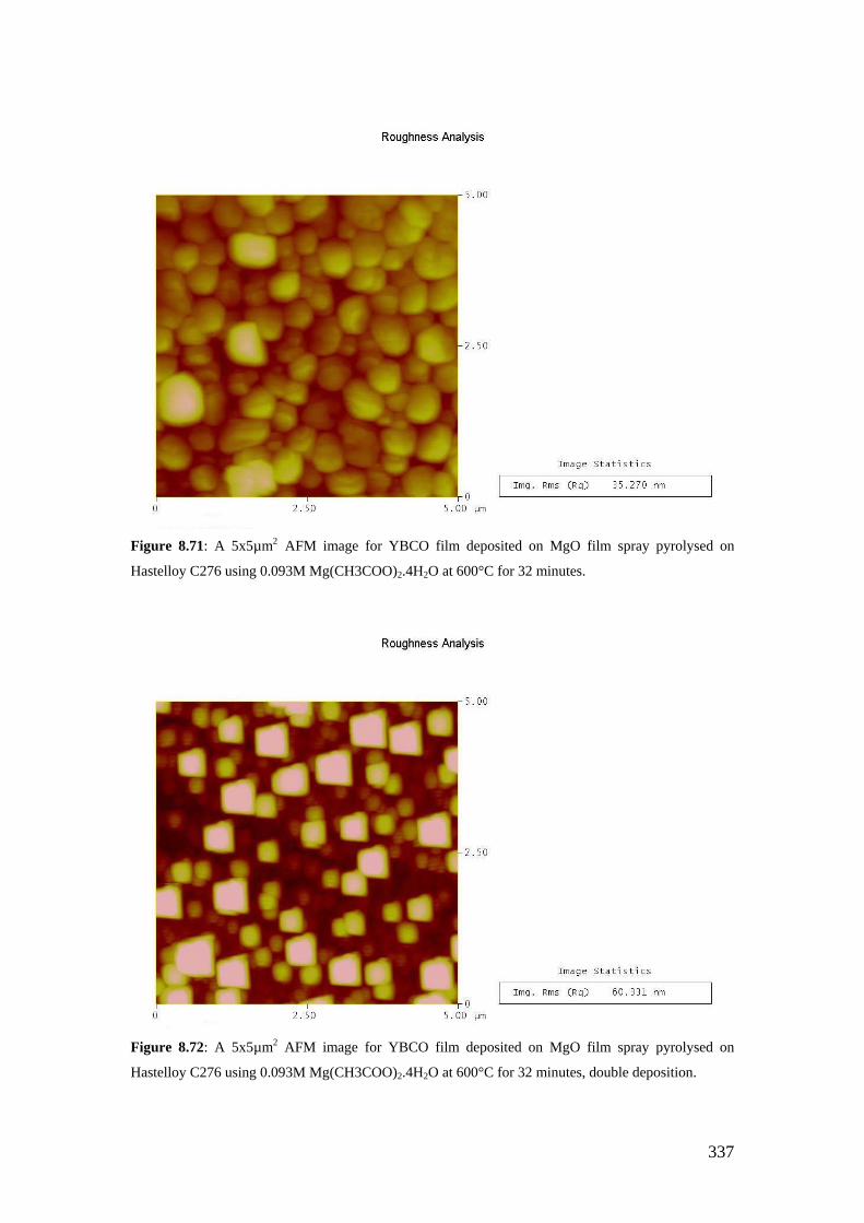
337
Figure 8.71: A 5x5µm2 AFM image for YBCO film deposited on MgO film spray pyrolysed on
Hastelloy C276 using 0.093M Mg(CH3COO)2.4H2O at 600°C for 32 minutes.
Figure 8.72: A 5x5µm2 AFM image for YBCO film deposited on MgO film spray pyrolysed on
Hastelloy C276 using 0.093M Mg(CH3COO)2.4H2O at 600°C for 32 minutes, double deposition.

338
Figure 8.73: A 5x5µm2 AFM image for YBCO film deposited on MgO film spray pyrolysed on
Hastelloy C276 using 0.14M Mg(CH3COO)2.4H2O at 600°C for 32 minutes.
Figure 8.74: EBSD pole figure pattern showing the {006} planes for YBCO film deposited by PLD on
Hastelloy substrate buffered with MgO deposited by spray pyrolysis at 550oC for 32 min. from 0.093M
Mg(CH3COO)2.4H2O.

339
Figure 8.75: EBSD pole figure pattern (left) and (001) X-ray pole figure (right), at 2θ of 46.65°,
showing the {006} planes for YBCO film deposited by PLD on Hastelloy substrate buffered with MgO
deposited by spray pyrolysis at 600oC for 32 min. from 0.093M Mg(CH3COO)2.4H2O.
0 10 20 30 40 50
Inte
nsity
(a. u
.)
ω scan (deg.)
Figure 8.76: X-ray diffraction ω−scan for YBCO film deposited on MgO film spray pyrolysed at
550°C from 0.093M solution showing YBCO (006) with a FWHM of 12.5ο.
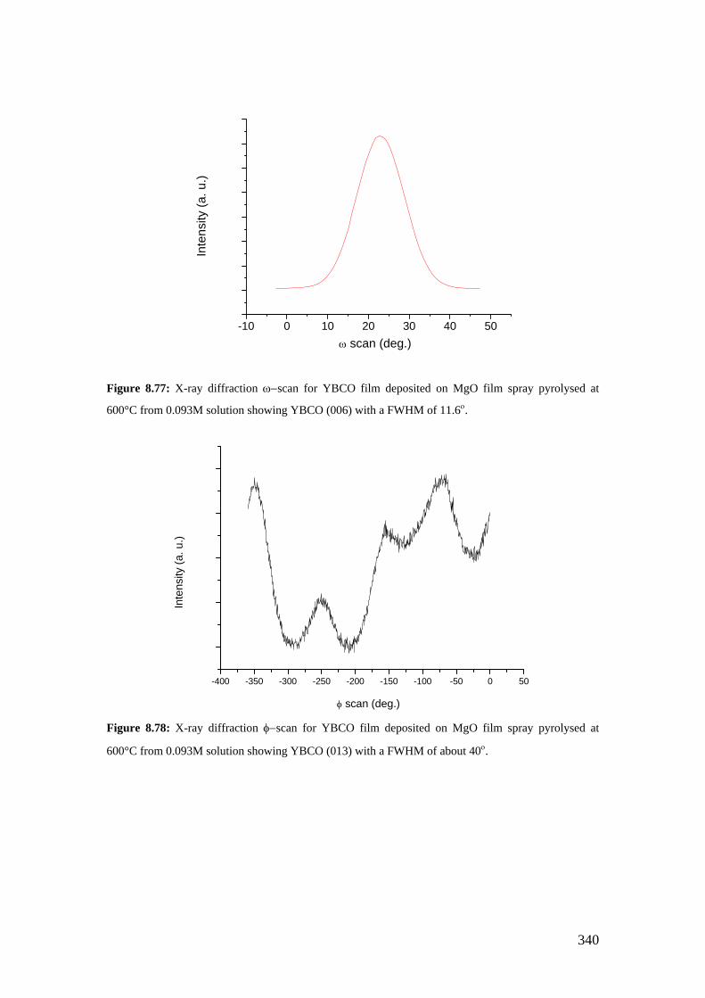
340
-10 0 10 20 30 40 50ω scan (deg.)
Inte
nsity
(a. u
.)
Figure 8.77: X-ray diffraction ω−scan for YBCO film deposited on MgO film spray pyrolysed at
600°C from 0.093M solution showing YBCO (006) with a FWHM of 11.6ο.
-400 -350 -300 -250 -200 -150 -100 -50 0 50
φ scan (deg.)
Inte
nsity
(a. u
.)
Figure 8.78: X-ray diffraction φ−scan for YBCO film deposited on MgO film spray pyrolysed at
600°C from 0.093M solution showing YBCO (013) with a FWHM of about 40ο.

341
Figure 8.79: EBSD histogram showing grain misorientation angles for YBCO film deposited on MgO
film spray pyrolysed on Hastelloy C276 using 0.093M Mg(CH3COO)2.4H2O at 550°C for 32 minutes.
Figure 8.80: EBSD histogram showing grain misorientation angles for YBCO film deposited on MgO
film spray pyrolysed on Hastelloy C276 using 0.093M Mg(CH3COO)2.4H2O at 600°C for 32 minutes.

342
Figure 8.81: Cross sectional SEM image of YBCO film deposited on MgO film spray pyrolysed on
Hastelloy C276 using 0.093M Mg(CH3COO)2.4H2O at 600°C for 32 minutes.
Figure 8.82: EDX line scan using 20KV of YBCO film deposited on MgO film spray pyrolysed on
Hastelloy C276 using 0.093M Mg(CH3COO)2.4H2O at 600°C for 32 minutes.
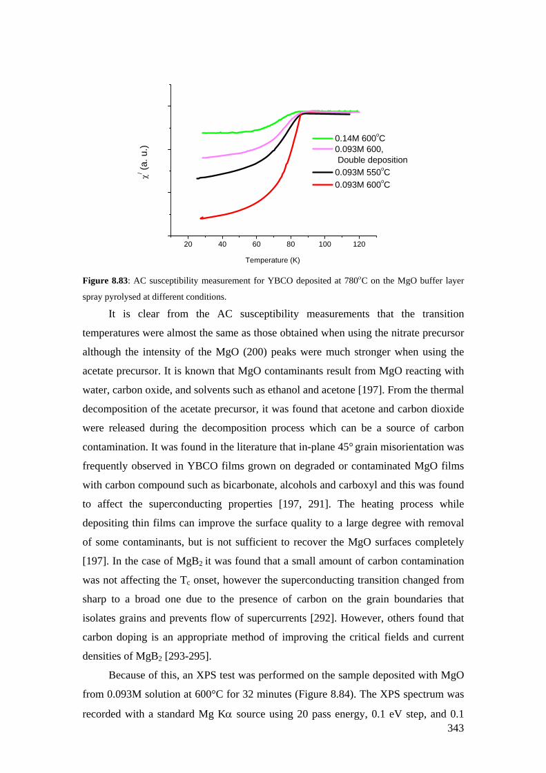
343
20 40 60 80 100 120
0.14M 600oC 0.093M 600,
Double deposition 0.093M 550oC 0.093M 600oC
Temperature (K)
χ/ (a. u
.)
Figure 8.83: AC susceptibility measurement for YBCO deposited at 780οC on the MgO buffer layer
spray pyrolysed at different conditions.
It is clear from the AC susceptibility measurements that the transition
temperatures were almost the same as those obtained when using the nitrate precursor
although the intensity of the MgO (200) peaks were much stronger when using the
acetate precursor. It is known that MgO contaminants result from MgO reacting with
water, carbon oxide, and solvents such as ethanol and acetone [197]. From the thermal
decomposition of the acetate precursor, it was found that acetone and carbon dioxide
were released during the decomposition process which can be a source of carbon
contamination. It was found in the literature that in-plane 45° grain misorientation was
frequently observed in YBCO films grown on degraded or contaminated MgO films
with carbon compound such as bicarbonate, alcohols and carboxyl and this was found
to affect the superconducting properties [197, 291]. The heating process while
depositing thin films can improve the surface quality to a large degree with removal
of some contaminants, but is not sufficient to recover the MgO surfaces completely
[197]. In the case of MgB2 it was found that a small amount of carbon contamination
was not affecting the Tc onset, however the superconducting transition changed from
sharp to a broad one due to the presence of carbon on the grain boundaries that
isolates grains and prevents flow of supercurrents [292]. However, others found that
carbon doping is an appropriate method of improving the critical fields and current
densities of MgB2 [293-295].
Because of this, an XPS test was performed on the sample deposited with MgO
from 0.093M solution at 600°C for 32 minutes (Figure 8.84). The XPS spectrum was
recorded with a standard Mg Kα source using 20 pass energy, 0.1 eV step, and 0.1

344
seconds per step for the detailed spectrum. The C 1S scan was from 270-300eV. A
peak was found at 284.9eV which corresponds to C 1s. Similar peaks were found by
others at 284.6 eV and 284.7 eV and was related to carbon based compounds or
hydrocarbon contaminants [197, 198, 291]. Therefore, the broad superconducting
transition temperatures can be related to carbon contamination from the thermal
decomposition of the acetate precursor. It is to be noted that XPS test performed on
the MgO film deposited from 0.468M solution of magnesium nitrate at 650°C for 48
minutes did not show any peaks corresponding to carbon contamination.
280 287 294
C 1S eV= 284.9 (carbon based compund or hydrocarbon)
Mg source270-300eV0.1eV step, 0.1 sec. dwell20 E pass
Inte
nsity
(a. u
.)
Binding Energy (eV) Figure 8.84: XPS spectrum for the MgO thin film deposited on Hastelloy C276 substrate using
0.093M Mg(CH3COO)2.4H2O at 600οC for 32 min. showing the C 1s.
8.11.3 Pulsed laser deposition of Ceria (CeO2) and YBCO on MgO
deposited by spray pyrolysis
It was found (section 8.11.2) that YBCO deposition on MgO films deposited by
spray pyrolysis resulted in YBCO films having very weak in-plane texture and with
broad superconducting transition temperatures. In an attempt to establish a good
in-plane texture, researchers found that the deposition of CeO2, in the ISD approach
using e-beam evaporation, will lead to a well defined and good in-plane textured
YBCO films [39, 41, 50, 169, 171, 177, 182, 183]. For this reason and to improve the
superconducting properties, and as was done with the nitrate precursor ( 7.12.4), CeO2
was deposited by PLD on top of MgO films deposited by spray pyrolysis followed by
YBCO deposition by PLD as well.
CeO2 was deposited at two different conditions. The used energy fluence was
2J/cm2, the distance between the target and the substrate was fixed at 56mm, 500 and

345
1000 pulses were applied as it was found by researchers that cracks will form in
100-200 nm thick CeO2 films [282-284]. The first deposition was made at 780°C
using 0.6 mbar O2 and the second one was made at 710°C using 2x10⁻⁴ mbar O2. The
YBCO deposition conditions were the same as those mentioned in section 7.12.1. The
deposition was made on the samples spray pyrolysed with MgO from 0.093M
solution at 600°C for 32 minutes.
The samples deposited with 500 pulses of CeO2 show very weak CeO2 peaks.
Therefore, the deposition proceeded from now on with only 1000 pulses. Figure 8.85
shows the XRD patterns for CeO2 films deposited on top of MgO deposited by spray
pyrolysis. The CeO2 peaks were indexed according to the JCPDS PDF file 00-004-
0593. It can be seen that none of the CeO2 deposition conditions resulted in a perfectly
(200) oriented films. However, the deposition at 780°C using 0.6 mbar O2 resulted in
a dramatic change giving a much stronger CeO2 (200) peak compared to the film
deposited at 710°C using 2x10⁻⁴ mbar O2. The surface roughness was increased after
the CeO2 deposition at 710°C using 2x10⁻⁴ mbar O2 as was clear from the SEM and
AFM images, in Figure 8.86 and Figure 8.88, respectively, compared to that before
the deposition (Figure 8.6 and Figure 8.8). However, CeO2 film deposited at 780°C
using 0.6 mbar O2 showed even a little smoother surface, as a result of the good
texture of CeO2, (Figure 8.87 and Figure 8.89) compared to that before deposition
(Figure 8.6 and Figure 8.8). The same observation was seen for low thicknesses of
CeO2 films on YSZ buffer which were deposited by PLD on ISD MgO deposited by
e-beam evaporation [169].
20 30 40 50 60 70
600oC 0.093M 32 min. Ceria 2x10⁻⁴mbar 710oC
600oC 0.093M 32 min. Ceria 0.6mbar 780oC
HC
(200
)
HC
(111
)M
gO (2
00)C
eO2 (
200)
CeO
2 (11
1)
Inte
nsity
(a. u
.)
2θ (degrees)
Figure 8.85: XRD patterns for CeO2 films deposited by PLD at different conditions on the MgO films
spray pyrolysed at 600°C from 0.093M for 32 minutes.

346
Figure 8.86: SEM image for CeO2 film deposited by PLD at 710°C using 2x10⁻⁴ mbar O2 on the MgO
film deposited by spray pyrolysis at 600°C from 0.093M for 32 minutes.
Figure 8.87: SEM image for CeO2 film deposited by PLD at 780°C using 0.6 mbar O2 on the MgO
film deposited by spray pyrolysis at 600°C from 0.093M for 32 minutes.

347
Figure 8.88: A 5x5µm2 AFM image for CeO2 film deposited by PLD at 710°C using 2x10⁻⁴ mbar O2
on the MgO film deposited by spray pyrolysis at 600°C from 0.093M for 32 minutes.
Figure 8.89: A 5x5µm2 AFM image for CeO2 film deposited by PLD at 780°C using 0.6 mbar O2 on
the MgO film deposited by spray pyrolysis at 600°C from 0.093M for 32 minutes.
To see the influence of the deposited CeO2 film on the properties the
superconducting layer, YBCO was deposited on each of the samples shown in Figure

348
8.85. Figure 8.90 shows the XRD patterns for YBCO films deposited on CeO2, and
Figure 8.91 and Figure 8.92 are the SEM images and the corresponding AFM images
are shown in Figure 8.93 and Figure 8.94. It is clear that the YBCO film had a
stronger (006) peak on the CeO2 film deposited at 780°C using 0.6 mbar O2. However,
the YBCO films were rougher (Figure 8.92-Figure 8.94) compared to the YBCO film
deposited directly on the MgO film deposited by spray pyrolysis (Figure 8.67 and
Figure 8.71). CeO2 film deposited at 780°C using 0.6 mbar resulted in a smoother
YBCO film when compared to the CeO2 film deposited at 710°C using 2x10⁻⁴ mbar.
This can be attributed to the smoother CeO2 film and stronger CeO2 (200) peak
deposited at 780°C using 0.6 mbar which gave stronger YBCO (006) peak and hence
smoother film. The thickness of the CeO2 should be in the range of 100nm as the
deposition conditions were the same as those obtained when using the nitrate
precursors (Figure 7.104).
The pole figure measurements show that YBCO had out-of-plane texture but
still no in-plane texture. This means that CeO2 deposition on the MgO deposited by
spray pyrolysis had no effect in improving the in-plane texture of the subsequent
YBCO layer which disagrees with what was found by other researchers [39, 41, 50,
169, 171, 177, 182, 183]. In addition to that, only the sample with CeO2 deposited
780°C using 0.6 mbar had a Tc (Figure 8.95) which was even worse compared to that
without CeO2 deposition (Figure 8.83).
0 10 20 30 40 50 60
YBC
O (0
07)
HC
(111
)
YBC
O (0
06)
HC
(111
)M
gO (2
00)
YBC
O (0
05)
YBC
O (1
03)
YBC
O (0
04)
CeO
2 (1
11)
YBC
O (0
03)
YBC
O (0
02)
Inte
nsity
(a. u
.)
2θ (degrees)
YBC
O (0
01)
600OC 0.093M 32 min Ceria 2X10⁻⁴mbar 710OC YBCO 0.6mbar 780OC
600OC 0.093M 32 min Ceria 0.6mbar 780OC YBCO 0.6mbar 780OC
Figure 8.90: XRD patterns for YBCO and CeO2 films deposited by PLD at different conditions on the
MgO films deposited by spray pyrolysis at 600°C from 0.093M for 32 minutes.

349
Figure 8.91: SEM image for YBCO on CeO2 film deposited by PLD at 710°C using 2x10⁻⁴ mbar O2 on
the MgO film deposited by spray pyrolysis at 600°C from 0.093M for 32 minutes.
Figure 8.92: SEM image for YBCO on CeO2 film deposited by PLD at 780°C using 0.6 mbar O2 on
the MgO film deposited by spray pyrolysis at 600°C from 0.093M for 32 minutes.

350
Figure 8.93: A 5x5µm2 AFM image for YBCO on CeO2 film deposited by PLD at 710°C using 2x10⁻⁴
mbar O2 on the MgO film deposited by spray pyrolysis at 600°C from 0.093M for 32 minutes.
Figure 8.94: A 5x5µm2 AFM image for YBCO on CeO2 film deposited by PLD at 780°C using 0.6
mbar O2 on the MgO film deposited by spray pyrolysis at 600°C from 0.093M for 32 minutes.
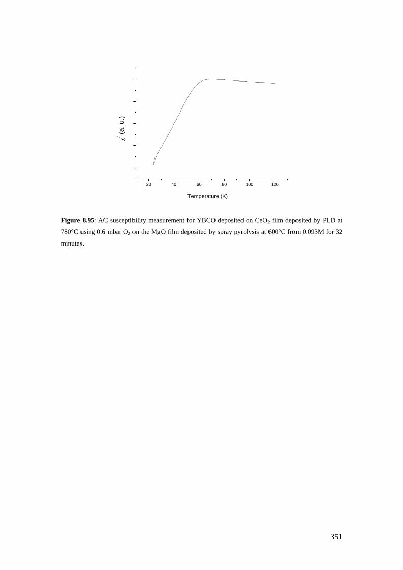
351
20 40 60 80 100 120
χ/ (a. u
.)
Temperature (K)
Figure 8.95: AC susceptibility measurement for YBCO deposited on CeO2 film deposited by PLD at
780°C using 0.6 mbar O2 on the MgO film deposited by spray pyrolysis at 600°C from 0.093M for 32
minutes.

352
9 Conclusions and future work

353
9.1 Introduction
MgO was deposited by spray pyrolysis on Si (100) single crystals, NiW tapes,
polycrystalline 310-austenitic stainless steel and Hastelloy C276. The deposition was
done at various conditions and different annealing treatments were performed on the
deposited MgO films. CeO2 was deposited by PLD on C276 buffered with MgO in an
attempt to improve the in-plane texture of the subsequent YBCO which was also
deposited by PLD.
9.1.1 Depositions on Si (100) single crystals using magnesium nitrate
precursor
The substrate temperature was found to affect the crystallinity of the produced
films, where at 600°C the films show very low intensity peaks with regard to MgO
(200). However, the films produced at 650°C and at 700°C were (200) textured,
irrespective of the precursor concentration. The MgO (200) peaks were strained due to
the thermal expansion coefficient mismatch between the Si substrate and MgO. It was
also found that the texture of MgO films improved with increasing the temperature
and concentration and that the surface morphology of the produced film was affected
by changing the substrate temperature from 650°C to 700°C.
At 650°C, the roughness increased by decreasing the concentration from
0.078M to 0.0078M. Conversely, at 700°C the roughness increased by increasing the
concentration from 0.0078M to 0.078M. The roughness at 700°C was also higher than
that at 650°C. The best film obtained was at 650°C from 0.078M solution and was
deposited according to the third mode of deposition and was biaxially textured.
It was found that the ISD affects the crystallinity of the deposited MgO films.
The intensity of MgO peaks and the thickness of MgO films decreased with
increasing the inclination angle. The thickness was increased with increasing the
concentration and the temperature. The deposition rate was found to depend on the
substrate temperature and concentration in direct proportionality and that the texture
improved with increasing thickness and temperature.
The roughness values, of the films produced at 650°C from 0.0078M, decreased
by increasing the inclination angle from zero to 20°, and then became independent on
the inclination angle from 20°-60°. At 0.078M, the roughness was almost independent

354
of the inclination angle. At 700°C the roughness decreased with increasing the
inclination angle. In all cases, the roughness at zero inclination was the highest.
Biaxially textured and epitaxial MgO film (MgO200//Si200 and MgO111//Si111)
was produced at 650°C from a 0.078M solution at zero degree inclination and by
inclining the substrate at 20°. The biaxially textured and epitaxial film deposited at
700° from 0.078M solution was also obtained by inclining the substrate at 20°.
However, the film had overgrown particles on the surface. From this it was concluded
that the ISD deposition by spray pyrolysis on Si substrates was not giving the
shadowing effect which produces c-axis tilted films.
MgO deposition by PLD was not as good as the films prepared by spray
pyrolysis due to the low fluence used during PLD deposition.
YBCO deposition on MgO films deposited by spray pyrolysis, at 650°C using
0.078M solution of magnesium nitrate with zero inclination angle, resulted in a very
weak superconducting transition temperature due to the thermal stresses developed in
the MgO buffer. YBCO deposition on MgO films deposited by spray pyrolysis under
other deposition conditions resulted in polycrystalline YBCO films with no Tc.
YBCO deposition on MgO films deposited by PLD resulted in no
superconductivity due to the weak texture of the deposited MgO buffer layer.
9.1.2 Depositions on NiW tapes using magnesium nitrate and acetate
precursors
The recrystallisation treatment of NiW tapes at 1100°C for 3 hours under
Ar-5%H2 atmosphere resulted in (200) textured tapes with a roughness of 14 nm and
after polishing they had a roughness of about 4 nm compared to 50 nm for the as
received substrates.
Deposition of MgO on recrystallised NiW tapes (i.e. (200) textured) resulted in
the formation of an amorphous MgO film. This was due to the instability of the
substrates during spray pyrolysis; where a polycrystalline NiO layer was formed.
Oxidation of recrystallised and unpolished NiW substrates at 1200°C under O2
atmosphere resulted in (200) textured NiO film which was epitaxial with the NiW
substrate, however, it was rotated 45° relative to the substrate. The texture was stable
even by heating the substrate to 780°C under vacuum which resembles YBCO
deposition conditions. The same texture relation was obtained after oxidising the

355
recrystallised and polished NiW substrates, however, the texture was disturbed when
heating the substrate to 780°C under the same YBCO deposition conditions.
MgO deposition on NiO (200) did not result in any MgO XRD peaks
irrespective of the used concentration or the used precursor (nitrate or acetate) and
was attributed to the surface instability of the oxide during the spray pyrolysis
deposition conditions.
9.1.3 Depositions on 310-austenitic stainless steel using magnesium
nitrate precursor
Magnesium nitrate was used as a precursor, however, no MgO XRD peaks were
observed (amorphous films were obtained) when using the 310-stainless steel as a
substrate regardless of the deposition temperate, deposition time and precursor
concentration. The oxalic acid test showed that the 310-austenitic stainless steels were
not severely affected and a dual etch structure was obtained; however, some carbides
were formed which disturbed the surface stability for MgO deposition. Therefore, it
was concluded that 310-St. St. is not a good candidate as a substrate material for
buffer layer deposition using the spray pyrolysis technique due to the thermal
instability of the surface during deposition at relatively high temperature and wet
environment.
9.1.4 Depositions on Hastelloy C276
This section is divided into two as the deposition of MgO was made on
Hastelloy C276 using nitrate and acetate precursors.
The corrosion rates for Hastelloy C276 obtained after conducting the boiling
iron (III) sulfate-sulfuric acid test was less than 1mm/month (the maximum allowable
corrosion rate). Therefore, C276 was a good candidate as a substrate material for
MgO deposition by spray pyrolysis. This was also confirmed by the SEM images
where only pits formed as a result of the long contact with the acid.
9.1.4.1 MgO deposition from the nitrate precursor
MgO deposition on C276 from nitrate precursor using 0.078M solution resulted
in the formation of amorphous MgO films irrespective of the deposition temperature
or deposition time. However, when using 0.468M solution at 650°C for 32 minutes a
weak MgO (200) peak was obtained. It was found that the peak intensity increased

356
with increasing the deposition time, deposition temperature, precursor concentration
or applying the double deposition process. However, this was at the expense of the
smoothness of the deposited MgO films.
The smooth MgO films deposited from 0.468M solution at 650°C for 32 and 48
minutes were deposited according to the third mode of deposition. The films
deposited at other deposition conditions were deposited mainly according to the fourth
mode of deposition except the ones deposited at 650°C for 64 minutes and 96 minutes
from 0.468M which needs be further investigated to determine the mode of
deposition. The films deposited from 0.78M solution were deposited according to the
second mode of deposition.
XPS results show that the surface of MgO was contaminated with hydroxide;
however, the MgO film was recovered during subsequent YBCO film deposition as
found in the literature that heating the contaminated layer to 450°C in air is sufficient
to regenerate the MgO surface [116].
Complete study on the effect of the thickness on the texture development was
difficult to achieve due to the difficulty in preparing cross sectional samples for the
thickness measurements. However, it was believed that the amorphous films obtained
when using the 0.078M solution was due to the low thicknesses of the deposited MgO
films. The MgO films deposited from 0.468M solution show a weak (200) texture.
This suggests that the texture developed with thickness and thickness increased with
increasing the concentration.
MgO deposition by inclining the substrate resulted in weaker MgO (200) peaks,
smoother surfaces and lower thicknesses compared to the films deposited with no
inclination.
Amorphous MgO films were obtained at low flow rates. The optimum Ar flow
rate was found to be 10 l/min which gave detectable MgO peaks and the smoothest
MgO films. Higher flow rate (15l/min) did not improve the texture of MgO films but
increased the roughness.
In an attempt to improve the texture of the MgO peaks, different annealing
treatments were performed. Annealing under O2 atmosphere up to 650°C had no effect
on the texture and roughness of the deposited MgO films. However, annealing at
800°C resulted in slight improvement in the intensity of MgO (200) peak but this was
at the expense of substrate oxidation. Annealing at 1000°C resulted in severe substrate
oxidation and no MgO peaks were detected. Annealing under vacuum up to 800°C

357
had no effect on the texture and smoothness of the MgO films. This confirmed the
stability of MgO under such conditions which is required for later YBCO deposition.
At 1000°C, the MgO peak disappeared due to Mg evaporation. Annealing under
purified Ar at 1000°C did not result in Mg evaporation, but resulted in rough MgO
films due to the high annealing temperature.
YBCO films deposited on MgO films, deposited by spray pyrolysis, with a
roughness greater than 20nm were polycrystalline and had no Tc. The MgO films,
deposited by spray pyrolysis, with a roughness of about 20nm had a weak in-plane
and out-of-plane texture. The films grow with the (200) normal to substrate surface as
distinct to MgO films grown by thermal evaporation which grow with the (200) tilted
to the substrate normal. Subsequent YBCO deposition on such MgO films were
textured with (006) being the strongest peak and have a slightly better out-of-plane
texture compared to the MgO buffer and (006) of YBCO // (200) of MgO. Thus, spray
pyrolysis offers an alternative method of depositing a single MgO buffer layer with no
tilting for YBCO deposition. However, the deposited YBCO films had a broad
superconducting transition temperature with a Tc onset of 84.5K. However, these
results demonstrate the potential for this chemical route to the deposition of a single
buffer layer of MgO with normal rather than tilted texture on a polycrystalline
technical substrate which could have significant impact on coated conductor
technology. YBCO films deposited on MgO films, deposited by spray pyrolysis at
different inclination angles, or using Ar flow rate of 5 and 15l/min, were
polycrystalline and had no Tc. The same result was found for YBCO films deposited
on the annealed MgO films.
CeO2 deposition on Hastelloy C276 buffered with MgO did not improve the
texture of the subsequent YBCO film or the transition temperature. It even made the
surface of MgO rougher and resulted in YBCO films with no Tc.
9.1.4.2 MgO deposition from the acetate precursor
MgO deposition from the acetate precursor resulted in stronger (200) oriented
films, even by using much lower concentration, compared to the nitrate precursor. The
intensity of MgO peak increased with increasing the deposition temperature,
deposition time, but this was at the expense of surface roughness. Increasing the
concentration did affect the intensity of MgO (200) peaks but increased the roughness
of the deposited films.

358
The smooth MgO films deposited from 0.093M solution at 500°C-600°C for 32
minutes were deposited according to the third mode of deposition. The films
deposited at 650°C were deposited according to the fourth mode of deposition. The
films deposited at 600°C from 0.093M for 64 minutes needs to be further investigated
to determine the mode of deposition and the films deposited at 600°C from 0.279M
for 32 minutes deposited according to the second mode of deposition.
XPS results show that the surface of MgO was contaminated with hydroxide,
however, the MgO film was recovered during subsequent YBCO film deposition as
found in the literature that heating the contaminated layer to 450°C in air is sufficient
to regenerate the MgO surface [116].
Complete study on the effect of the thickness on the texture development was
difficult to achieve due to the difficulty in preparing cross sectional samples for the
thickness measurements.
MgO deposition by inclining the substrate resulted in weaker MgO (200) peaks,
smoother surfaces and lower thicknesses compared to the films deposited with no
inclination.
The optimum Ar flow rate was found to be 10 l/min which gave detectable MgO
peaks and the smooth MgO films. Higher (15 l/min) and lower (15 l/min) flow rates
resulted in smooth films but with low intensity MgO peaks.
In an attempt to improve the texture of MgO peaks, different annealing
treatments were performed. Annealing under O2 atmosphere up to 650°C had no effect
on the texture and roughness of the deposited MgO films. However, annealing at
800°C 1000°C resulted in substrate oxidation. Annealing under vacuum up to 800°C
had no effect on the texture and smoothness of the MgO films. This confirmed the
stability of MgO under such conditions which is required for later YBCO deposition.
At 1000°C, the MgO peak disappeared due to Mg evaporation. Annealing under
purified Ar at 1000°C resulted in partial Mg evaporation and led to the formation of
rough films due to the high annealing temperature.
YBCO films deposited on MgO films, deposited by spray pyrolysis, with a
roughness greater than about 42nm were polycrystalline and had no Tc. The MgO
films, deposited by spray pyrolysis, with a roughness up to 42 nm had a weak in-plane
and out-of-plane texture but better than those obtained when the magnesium nitrate
precursor was used. The films grow with the (200) normal to substrate surface as
distinct to MgO films grown by thermal evaporation which grow with the (200) tilted

359
to the substrate normal. Subsequent YBCO deposition on such MgO films were
textured with (006) being the strongest peak and (006) of YBCO // (200) of MgO.
Thus, spray pyrolysis offers an alternative method of depositing a single MgO buffer
layer with no tilting for YBCO deposition. However, the deposited YBCO film had a
broad superconducting transition temperature with a Tc onset of 84.8K. However,
these results demonstrate the potential for this chemical route to the deposition of a
single buffer layer of MgO with normal rather than tilted texture on a polycrystalline
technical substrate which could have significant impact on coated conductor
technology. The best texture, surface smoothness and Tc were obtained for the film
deposited at 600°C using 0.093M for 32 minutes; besides that, an EDX line scan
performed on such samples improved the effectiveness of MgO as a diffusion barrier
layer. However, the superconducting transition temperatures were not improved
compared to those when using the nitrate precursor although the acetate precursor
gave stronger MgO (200) peaks and that was related to carbon contamination. YBCO
films deposited on MgO films, deposited by spray pyrolysis at different inclination
angles, or using Ar flow rate of 5 and 15 l/min, were polycrystalline and had no Tc.
The same result was found for YBCO films deposited on the annealed MgO films.
CeO2 deposition on Hastelloy C276 buffered with MgO did not improve the
texture of the subsequent YBCO film or the transition temperature. The best YBCO
films were those deposited on CeO2 films deposited by PLD at 780°C using 0.6 mbar
O2 on the MgO films deposited by spray pyrolysis at 600°C from 0.093M for 32
minutes. However, the AC susceptibility measurement showed a bad superconducting
transition temperature compared to that before CeO2 deposition.
9.2 Suggestions for future work
Many parameters for the deposition of MgO by spray pyrolysis were
investigated, however, due to the lack of time, some other parameters need to be
investigated and some process modifications may need to be made.
9.2.1 Deposition of MgO thin films
It was noticed that higher Mg(NO3)2.6H2O concentrations were needed to obtain
a (200) oriented MgO films compared to that when using the Mg(CH3COO)2.4H2O
precursor. This was believed to be due to a high vapour pressure of the Mg2+ when

360
using low concentrations of Mg(NO3)2.6H2O; however this behaviour was not really
understood and needs further investigation.
It was found that the broad superconducting transition temperatures can be
attributed to carbon contamination from the acetate precursors. An Ar ion beam etch
(IBE) cleaning process at low ion energy can be used to refresh the MgO surfaces
[197, 198] and this may improve the transition temperatures.
CeO2 deposition was found to improve the in-plane texture of the subsequent
YBCO films; however, when deposited on MgO films deposited by spray pyrolysis, it
did not; therefore, other buffer layers such as SrTiO3 (STO) could be utilized for
investigating this purpose.
Some of the parameters during the spray pyrolysis deposition were not
investigated. These include: nozzle diameter, substrate-nozzle distance and the type of
carrier gas which would be some suggestions for future work.
When depositing MgO films on metallic substrates, it was difficult to prepare
cross sections to study the effect of thickness on the deposited MgO, CeO2 and YBCO
films. The use of focused ion beam (FIB) milling to prepare samples, where many
problems associated with the mechanical preparation are eliminated, would be the
solution.
The metallic substrates, especially NiW and 310-austenitic stainless steel
substrates were not stable under the spray pyrolysis deposition conditions which
provided wet environments that affected the stability of the substrates for thin film
deposition. Therefore, ethanol or methanol solvents may be used to deposit MgO
films on such substrates and its effect on substrate surface stability should be
investigated.
To further investigate the deposited MgO films from the nitrate and acetate
precursors, TEM samples would be of interest to study the growth behaviour and
effect of thickness on the deposited thin films of MgO, CeO2 and YBCO. In addition,
performing an EDX profile scan across the substrate-MgO film interface could be
made to confirm the effectives of MgO as a diffusion barrier layer.
The adhesion of MgO and YBCO films would be another issue that should be
investigated on different substrates i.e. on Si single crystals and Hastelloy C276; as
the MgO peaks were relatively strong on such substrates but the superconducting
transition temperatures were broad.

361
9.2.2 System modification
To increase the amount of aerosol deposition, electrostatic spraying can be
utilized by applying a DC voltage between the nozzle and the substrate; however, in
this case the substrates are limited to conductive ones.
As mentioned earlier about the substrate instability under the spray pyrolysis
conditions, a simple vacuum system may be incorporated in addition to the use of
alcoholic solvents as an attempt to solve this problem.
It was found that the temperature of the substrate decreased during the spraying
process which forced the use of pulse time to interval time of 1:7. To speed the
process, the use of multi-zone tubular furnace may be beneficial to heat the aerosol
stream in a more controlled manner before it reaches the substrate.

362
List of References
[1] Concise encyclopaedia of magnetic and superconducting materials First ed. J. E. Evetts, Frs, R.W.C, Bever, M. B., editor. OXFORD, NEW YORK, SEOUL, TOKYO: Pergammon Press; 1992. [2] Lennard G,Richard E. Superconductivity: an overview Congressional Research Service. 1987: 1-11 [3] Superconductivity: the Meissner effect, Persistent currents, and the Josephson effects. MIT deptof physics. 2003: 1-16 [4] Handbook of applied superconductivity S. Berned, editor. Bristol and Philadelphia: IOP Publishing Ltd; 1998. [5] Woods Halley J. Theories of high temperature superconductivity. Allan, M. Wyylde; 1988. [6] Goyal A, Norton DP, Christen DK, Specht ED, Paranthaman M, Kroeger DM, et al. Epitaxial superconductors on rolling-assisted biaxially-textured substrates (RABiTS): A route towards high critical current density wire. Applied Superconductivity. 1996;4(10-11):403-427. [7] Bednorz JG,Müller KA. Possible highTc superconductivity in the Ba−La−Cu−O system. Zeitschrift für Physik B Condensed Matter. 1986;64(2):189-193. [8] Wu MK, Ashburn JR, Torng CJ, Hor PH, Meng RL, Gao L, et al. Superconductivity at 93 K in a new mixed-phase Y-Ba-Cu-O compound system at ambient pressure. Physical Review Letters. 1987;58(9):908. [9] Superconductivity Harvard, University; [cited 2007 May 12th]; Available from: http://hoffman.physics.harvard.edu/research/SCintro.php [10] Michael T. Introduction to Superconductivity. McGraw-Hill, Inc.; 1976. [11] Parks RD. Superconductivity. Marcel Dekker INC.; 1969. [12] Thompson DJ, Minhaj MSM, Wenger LE,Chen JT. Observation of Paramagnetic Meissner Effect in Niobium Disks. Physical Review Letters. 1995;75(3):529-532. [13] Kuppusami P,Raghunathan VS. Processing and properties of thin films of high critical temperature superconductors. International Materials Reviews. 2003;48(1):1-43. [14] Type II Superconductors. Mit,; [cited 2007 May 12th]; Available from: http://web.mit.edu/6.763/www/FT03/Lectures/Lecture17.pdf [15] Amit G. Second Generatin HTS Conductors. Kluwer Academic Publishers; 2005.

363
[16] Goyal A, Paranthaman MP,Schoop U. The RABiTS approach: Using rolling-assisted biaxially textured substrates for high-performance YBCO superconductors. Mrs Bulletin. 2004;29(8):552-561. [17] Kim K, Paranthaman M, Norton DP, Aytug T, Cantoni C, Gapud AA, et al. A perspective on conducting oxide buffers for Cu-based YBCO-coated conductors. Supercond Sci Technol. 2006;19(4):R23-R29. [18] Riley GN, Li Q,Fritzemeier LG. High temperature superconducting composite wires. Current Opinion in Solid State and Materials Science. 1999;4(5):473-478. [19] Heine K, Tenbrink J,Thoner M. High-field critical current densities in Bi2Sr2Ca1Cu2O8+x/Ag wires. Applied Physics Letters. 1989 Dec;55(23):2441-2443. [20] Glowacki BA, editor. Texture development of HTS powder-in-tube conductors. International Symposium on Processing and Critical Current of High-Temperature Semiconductors; 1998 Feb 02-04; Wagga Wagga, Australia. Iop Publishing Ltd. [21] Handbook of superconducting materials A. David Cardwell and S. David Ginley, editors. Brisyol and Philadelphia: IoP; 2003. [22] Feldmann DM, Holesinger TG, Cantoni C, Feenstra R, Nelson NA, Larbalestier DC, et al. Grain orientations and grain boundary networks of YBa2Cu3O7-delta films deposited by metalorganic and pulsed laser deposition on biaxially textured Ni-W substrates. J Mater Res. 2006;21(4):923-934. [23] Shields TC, Kawano K, Button TW,Abell JS. Spray pyrolysis of epitaxial YBCO films on (100) single crystal SrTiO3 substrates. Supercond Sci Technol. 2002;15(1):99-103. [24] Shields TC, Abell JS, Button TW, Chakalov RA, Chakalova RI, Cai C, et al. Deposition of YBCO films by high temperature spray pyrolysis. Physica C-Superconductivity and Its Applications. 2002;372:747-750. [25] Schieber M, Han SC, Ariel Y, Chokron S, Tsach T, Maharizi M, et al. Comparison of thin films of YBa2Cu3O7-x deposited by physical (laser ablation) and chemical (OMCVD) methods for device applications. Journal of Crystal Growth. 1991;115(1-4):31-42. [26] Sheth A, Schmidt H,Lasrado V. Review and evaluation of methods for application of epitaxial buffer and superconductor layers. Applied Superconductivity. 1999;6(10-12):855-873. [27] Cantoni C, Aytug T, Verebelyi DT, Paranthaman M, Specht ED, Norton DP, et al. Conductive buffer layers and overlayers for the thermal stability of coated conductors. Applied Superconductivity, IEEE Transactions on. 2001;11(1):3309-3312.

364
[28] Superconducting Coated Conductors University of Cambridge; [cited 2007 May 12th]; Available from: http://www-dmg.msm.cam.ac.uk/ResearchNew/Appl_Sup/CoatedConductors/calcium.html. [29] Wordenweber R. Growth of high-Tc thin films. Superconductor Science and Technology. 1999;12(6):R86-R102. [30] Dimos D, Chaudhari P, Mannhart J,Legoues FK. Orientation Dependence of Grain-Boundary Critical Currents in Yba2Cu3O7-Delta Bicrystals. Physical Review Letters. 1988;61(2):219-222. [31] Huhne R, Beyer C, Holzapfel B, Oertel CG, Schultz L,Skrotzki W. Growth of biaxial textured MgO-Layers by ion-beam assisted pulsed laser deposition. Crystal Research and Technology. 2000;35(4):419-425. [32] Bhattacharjee PP, Ray RK,Upadhyaya A. Nickel base substrate tapes for coated superconductor applications. Journal of Materials Science. 2007;42(6):1984-2001. [33] MacManus-Driscoll JL. Recent developments in conductor processing of high irreversibility field superconductors. Annual Review of Materials Science. 1998;28:421-462. [34] Paranthaman MP, Aytug T, Zhai HY, Heatherly L, Goyal A,Christen DK. Growth of YBCO films on MgO-based rolling-assisted biaxially textured substrates templates. Supercond Sci Technol. 2005;18(3):223-228. [35] Mao Y, Ren C, Yuan J, Zhang F, Liu X, Zou S, et al. Ion beam assisted deposition of biaxially textured YSZ thin films as buffer layers for YBCO superconducting films. Physica C: Superconductivity. 1997;282-287(Part 2):611-612. [36] Hirvonen JK. Ion-Beam Assisted Thin-Film Deposition. Materials Science Reports. 1991;6(6):215-274. [37] Iijima Y, Kakimoto K, Sutoh Y, Ajimura S,Saitoh T. Development of long Y-123 coated conductors for coil-applications by IBAD/PLD method. Ieee Transactions on Applied Superconductivity. 2005;15(2):2590-2595. [38] Brewer RT, Hartman JW, Groves JR, Arendt PN, Yashar PC,Atwater HA. Rheed in-plane rocking curve analysis of biaxially-textured polycrystalline MgO films on amorphous substrates grown by ion beam-assisted deposition. Applied Surface Science. 2001;175:691-696. [39] Ma B, Koritala RE, Fisher BL, Uprety KK, Baurceanu R, Dorris SE, et al. High critical current density of YBCO coated conductors fabricated by inclined substrate deposition. Physica C: Superconductivity. 2004;403(3):183-190. [40] Ma B, Li M, Fisher BL, Koritala RE,Balachandran U. Inclined-substrate deposition of biaxially aligned template films for YBCO-coated conductors. Physica C: Superconductivity. 2002;382(1):38-42.

365
[41] Li M, Ma B, Koritala RE, Fisher BL, Zhao X, Maroni VA, et al. c-Axis orientation control of YBa2Cu3O7-x films grown on inclined-substrate-deposited MgO-buffered metallic substrates. Solid State Communications. 2004;131(2):101-105. [42] Wong-Ng W, Levin I, Feenstra R, Cook LP,Vaudin M. Phase evolution of Ba2YCu3O6+x films during the BaF2 process. Supercond Sci Technol. 2004;17(9):S548-S556. [43] Goyal A, List FA, Mathis J, Paranthaman M, Specht ED, Norton DP, et al. High critical current density YBa2Cu3Ox tapes using the RABiTs approach. Journal of Superconductivity. 1998;11(5):481-487. [44] Goyal A, Norton DP, Kroeger DM, Christen DK, Paranthaman M, Specht ED, et al. Conductors with controlled grain boundaries: An approach to the next generation, high temperature superconducting wire. J Mater Res. 1997;12(11):2924-2940. [45] Vannozzi A, Rufoloni A, Celentano G, Augieri A, Ciontea L, Fabbri F, et al. Cube-textured substrates for YBCO-coated conductors: microstructure evolution and stability. Supercond Sci Technol. 2006;19(12):1240-1245. [46] Goyal A, Ren SX, Specht ED, Kroeger DM, Feenstra R, Norton D, et al. Texture formation and grain boundary networks in rolling assisted biaxially textured substrates and in epitaxial YBCO films on such substrates. Micron. 1999;30(5):463-478. [47] Vallejo RN,Wu JZ. Ion beam assisted deposition of textured magnesium oxide templates on un-buffered glass and silicon substrates. J Mater Res. 2006;21(1):194-198. [48] Mohan S,Krishna MG. A review of ion beam assisted deposition of optical thin films. Vacuum. 1995;46(7):645-659. [49] Hasegawa K, Fujino K, Mukai H, Konishi M, Hayashi K, Sato K, et al. Biaxially aligned YBCO film tapes fabricated by all pulsed laser deposition. Applied Superconductivity. 1996;4(10-11):487-493. [50] Ma B, Li M, Jee YA, Koritala RE, Fisher BL,Balachandran U. Inclined-substrate deposition of biaxially textured magnesium oxide thin films for YBCO coated conductors. Physica C: Superconductivity. 2002;366(4):270-276. [51] Ghekiere P, Mahieu S, De Winter G, De Gryse R,Depla D. Influence of the deposition parameters on the biaxial alignment of MgO grown by unbalanced magnetron sputtering. Journal of Crystal Growth. 2004;271(3-4):462-468. [52] Balachandran U, Li M, Koritala RE, Fisher BF,Ma B. Development of YBCO-coated conductors for electric power applications. Physica C: Superconductivity. 2002;372-376(Part 2):869-872.

366
[53] Balachandran U, Ma B, Li A, Fisher BL, Koritala RE, Erck RA, et al. Inclined-substrate deposition of biaxially textured template for coated conductors. Physica C-Superconductivity and Its Applications. 2002;378:950-954. [54] Wei M, Zhi D,Choy KL. Electrostatic spray assisted vapour deposition and structural characterisation of cerium oxide films on biaxially textured Ni tapes. Materials Letters. 2006;60(12):1519-1523. [55] Xiong J, Chen Y, Qiu Y, Tao BW, Qin WF, Cui XM, et al. A novel process for CeO2 single buffer layer on biaxially textured metal substrates in YBCO coated conductors. Supercond Sci Technol. 2006;19(10):1068-1072. [56] Rhee SH, Yang Y, Choi HS, Myoung JM,Kim K. Low-temperature deposition of highly [100]-oriented MgO films using charged liquid cluster beam. Thin Solid Films. 2001;396(1-2):23-28. [57] Bhattacharya RN, Phok S, Xu YL,Bhattacharya R. Electrodeposited biaxially textured buffer layers for YBCO superconductors. Ieee Transactions on Applied Superconductivity. 2007;17(2):3321-3324. [58] Carlson CM, Price JC, Parilla PA, Ginley DS, Niles D, Blaugher RD, et al. Laser-ablated epitaxial LaAlO3 buffer layers on biaxially textured Ni substrates for superconducting tapes. Physica C: Superconductivity. 1998;304(1-2):82-88. [59] Chung JK, Ko RK, Shi DQ, Ha HS, Kim H, Song KK, et al. Use of SrTiO3 as a single buffer layer for RABiTS YBCO coated conductor. Ieee Transactions on Applied Superconductivity. 2005;15(2):3020-3023. [60] Park C, Norton DP, Lee DF, Verebelyi DT, Goyal A, Christen DK, et al. Epitaxial yttria-stabilized zirconia on biaxially-textured (001) Ni for YBCO coated conductor. Physica C: Superconductivity. 2000;341-348(Part 4):2481-2482. [61] He Q, Christen DK, Budai JD, Specht ED, Lee DF, Goyal A, et al. Deposition of biaxially-oriented metal and oxide buffer-layer films on textured Ni tapes: New substrates for high-current, high-temperature superconductors. Physica C. 1997;275(1-2):155-161. [62] Konstantinov K, Stambolova I, Peshev P, Darriet B,Vassilev S. Preparation of ceria films by spray pyrolysis method. International Journal of Inorganic Materials. 2000;2(2-3):277-280. [63] Petrova NL, Todorovska RV,Todorovsky DS. Spray-pyrolysis deposition of CeO2 thin films using citric or tartaric complexes as starting materials. Solid State Ionics. 2006;177(5-6):613-621. [64] Kim HJ, Joo J, Ji BK, Jun BH, Jung CH, Park SD, et al. Deposition of CeO2 buffer layers for YBCO coated conductors on biaxially textured ni substrates by MOCVD technique. Ieee Transactions on Applied Superconductivity. 2003;13(2):2555-2558.

367
[65] Bian JM, Li XM, Chen TL, Gao XD,Yu WD. Preparation of high quality MgO thin films by ultrasonic spray pyrolysis. Applied Surface Science. 2004;228(1-4):297-301. [66] Jergel M, Chromik S, Strbik V, Smatko V, Hanic F, Plesch G, et al. Thin YBCO films prepared by low-temperature spray pyrolysis. Supercond Sci Technol. 1992;5:225-230 [67] Stambolova I, Konstantinov K, Kovacheva D, Khristov M, Peshev P,Donchev T. Spray pyrolysis deposition of polycrystalline magnesia films and their use as buffer layers in Bi(Pb)-Sr-Ca-Cu-O/MgO/Al2O3 (or glass ceramics) structures. Materials Letters. 1997;30(5-6):333-337. [68] Ghekiere P, Mahieu S, De Gryse R,Depla D. Structure evolution of the biaxial alignment in sputter-deposited MgO and Cr. Thin Solid Films. 2006;515(2):485-488. [69] Kingery DD, Bowen HK,Uhlmann DR. Introduction to ceramics. John wiley & sons, 1976; 1960. [70] William D. Callister J. Fundamentals of Materials Science and Engineering. John Wiley & Sons, Inc.; 2001. [71] Lee SY, Lee SH, Nah EJ, Lee SS,Kim Y. Heteroepitaxial growth of MgO films on Si(0 0 1) substrates using cubic SiC as a buffer layer. Journal of Crystal Growth. 2002;236(4):635-639. [72] Fu X, Wu G, Song S, Song Z, Duo X,Lin C. Preparation and characterization of MgO thin films by a simple nebulized spray pyrolysis technique. Applied Surface Science. 1999;148(3-4):223-228. [73] Pradhan AK, Sahu DR, Roul BK,Feng Y. Lanthanum-based manganite films on MgO using SrTiO3 as a template layer. Journal of Applied Physics. 2004;96(2):1170-1173. [74] Gila BP, Kim J, Luo B, Onstine A, Johnson W, Ren F, et al. Advantages and limitations of MgO as a dielectric for GaN. Solid-State Electronics. 2003;47(12):2139-2142. [75] Caceres D, Vergara I,Gonzalez R. Microstructural characterization of MgO thin films grown by radio-frequency sputtering. Target and substrate-temperature effect. Journal of Applied Physics. 2003;93(7):4300-4305. [76] Hellman ES,Hartford EH. Epitaxial Solid-Solution Films of Immiscible MgO and CaO. Applied Physics Letters. 1994;64(11):1341-1343. [77] Niu F, Hoerman BH,Wessels BW. Epitaxial thin films of MgO on Si using metalorganic molecular beam epitaxy. Journal of Vacuum Science & Technology B. 2000;18(4):2146-2152.
368
[78] Yi X, Wenzhong W, Yitai Q, Li Y,Zhiwen C. Deposition and microstructural characterization of MgO thin films by a spray pyrolysis method. Surface and Coatings Technology. 1996;82(3):291-293. [79] One-electron properties Crystal; [cited 2008 May, 12th]; Available from: http://www.crystal.unito.it/mssc2006_cd/tutorials/surfaces/surfaces_tut.html. [80] Fork DK, Nashimoto K,Geballe TH. Epitaxial Yba2Cu3O7-Delta on GaAs(001) Using Buffer Layers. Applied Physics Letters. 1992;60(13):1621-1623. [81] Tarsa EJ, De Graef M, Clarke DR, Gossard AC,Speck JS. Growth and characterization of (111) and (001) oriented MgO films on (001) GaAs. Journal of Applied Physics. 1993;73(7):3276-3283. [82] Hung LS, Zheng LR,Blanton TN. Epitaxial growth of MgO on (100) GaAs using ultrahigh vacuum electron-beam evaporation. Applied Physics Letters. 1992;60(25):3129-3131. [83] Milan J. Synthesis of high-Tc superconducting films by deposition from an aerosol. Supercond Sci Technol. 1995;8:67-78. [84] Danius P,Ludwig J. Thin film deosition using spray pyrlolysis. Journal of electroceramics. 2005;14(2):103-111. [85] Boo JH, Yu KS, Koh W,Kim Y. Preparation of MgO films on GaAs by metalorganic chemical vapor deposition. Materials Letters. 1996;26(4-5):233-236. [86] Kim SG, Kim JY,Kim HJ. Deposition of MgO thin films by modified electrostatic spray pyrolysis method. Thin Solid Films. 2000;376(1-2):110-114. [87] Liu M, Liu DM, Zhou ML, Zhao Y, Gao X,Liang JX. Fabrication of YBCO tapes on Ag substrates by the ultrasonic spray pyrolysis method. Supercond Sci Technol. 2004 Apr;17(4):676-680. [88] Mateev E, Donchev T, Blagoev B, Nurgaliev T, Tsaneva V,Barber ZH. Deposition of YBa2Cu3O7-x superconducting films by magnetron sputtering and water vapour addition to the sputtering gas. Vacuum. 2004;76(2-3):241-244. [89] Goyal A, Norton DP, Budai JD, Paranthaman M, Specht ED, Kroeger DM, et al. High critical current density superconducting tapes by epitaxial deposition of YBa2Cu3Ox thick films on biaxially textured metals. Applied Physics Letters. 1996;69(12):1795-1797. [90] Takechi A, Matsumoto K,Osamura K. YBa2Cu3O7-x films on oxide buffer layer with perovskite structure prepared by metal-organic deposition method. Physica C: Superconductivity. 2003;392-396(Part 2):895-899. [91] Marguillier D, Cloots R, Rulmont A, Fagnard JF, Vanderbemden P,Ausloos M. YBa2Cu3O7 tapes prepared by sol-gel deposition techniques: microstructure and
369
structural characterizations. Physica C: Superconductivity. 2002;372-376(Part 2):715-718. [92] Wesolowski DE, Yoshizumi M,Cima MJ. Trajectory-property relationships in MOD-derived YBCO films. Physica C: Superconductivity. 2006;450(1-2):76-82. [93] Vergnieres L, Donet S, Jimenez C, Odier P, Weiss F, Bruzek CE, et al. MOCVD and spray pyrolysis for coated conductor synthesis. Ieee Transactions on Applied Superconductivity. 2005;15(2):2759-2762. [94] Vergnieres L, Odier P, Weiss F, Bruzek CE,Saugrain JM. Epitaxial thick films by spray pyrolysis for coated conductors. Journal of the European Ceramic Society. 2005;25(12):2951-2954. [95] Méchin L, Villégier J-C, Rolland G,Laugier F. Double CeO2/YSZ buffer layer for the epitaxial growth of YBa2Cu3O7-delta films on Si (001) substrates. Physica C: Superconductivity. 1996;269(1-2):124-130. [96] Qiao JM,Yang CY. High-Tc superconductors on buffered silicon - materials properties and device applications. Materials Science & Engineering R-Reports. 1995 Apr;14(4):157-201. [97] High-Temperature Superconductivity Helsinki Univeristy of Technology; [cited 2008 May 19th]; Available from: http://www.tkk.fi/Units/AES/projects/prlaser/supercond.htm. [98] Jorgensen JD, Veal BW, Paulikas AP, Nowicki LJ, Crabtree GW, Claus H, et al. Structural properties of oxygen-deficient YBa2Cu3O7- delta. Physical Review B. 1990;41(4):1863. [99] Jeong YS, Park JH,Lee SY. Epitaxial growth of YBCO on Hastelloy with YSZ buffer layer by laser ablation. Thin Solid Films. 1998;318(1-2):262-264. [100] Russo RE, Reade RP, McMillan JM,Olsen BL. Metal buffer layers and Y-Ba-Cu-O thin films on Pt and stainless steel using pulsed laser deposition. Journal of Applied Physics. 1990;68(3):1354-1356. [101] Fukui S, Kojima R, Ogawa J, Yamaguchi M, Sato T,Tsukamoto O. Numerical analysis of AC loss characteristics of cable conductor assembled by HTS tapes in polygonal arrangement. Ieee Transactions on Applied Superconductivity. 2006;16(2):143-146. [102] Donald LS. Thin-Film Deposition Principles and Practices. McGraw-ill; 1995. [103] Woodcock TG. The crystallographic texture and morphology of nickel oxide layers grown on textured nickel and nickel alloy substrates [PhD Thesis]. Birmingham: University of Birmingham; July 2003.

370
[104] Narumi E, Song LW, Yang F, Patel S, Kao YH,Shaw DT. Critical current density enhancement in YBa2Cu3O6.8 films on buffered metallic substrates. Applied Physics Letters. 1991;58(11):1202-1204. [105] Reade RP, Mao XL,Russo RE. Characterization of Y-Ba-Cu-O thin films and yttria-stabilized zirconia intermediate layers on metal alloys grown by pulsed laser deposition. Applied Physics Letters. 1991;59(6):739-741. [106] Lewis JR. A dictionary of metallurgy. S. K. Jain 1997. [107] Chopra KL. Thin film phenomena New York ; London McGraw-Hill; 1969. [108] Herman MA, Richter, Wolfgang, Sitter, Helmut. Epitaxy : physical principles and technical implementation First ed. Berlin ; London Springer; 2004. [109] Thompson CV, Floro J,Smith HI. Epitaxial grain growth in thin metal films. Journal of Applied Physics. 1990;67(9):4099-4104. [110] Toivo TK,Mark JH. Aerosol processing of materials. New York: WILEY-VCH; 1999. [111] Che S, Sakurai O, Shinozaki K,Mizutani N. Particle structure control through intraparticle reactions by spray pyrolysis. Journal of Aerosol Science. 1998;29(3):271-278. [112] Chamberlin RR,Skarman JS. Chemical Spray Deposition Process for Inorganic Films. Journal of the Electrochemical Society. 1966;113(1):86-89. [113] Patil PS. Versatility of chemical spray pyrolysis technique. Materials Chemistry and Physics. 1999;59(3):185-198. [114] Paraguay F, Estrada W, Acosta DR, Andrade E,Miki-Yoshida M. Growth, structure and optical characterization of high quality ZnO thin films obtained by spray pyrolysis. Thin Solid Films. 1999;350(1-2):192-202. [115] Ban E, Matsuoka Y, Ogawa H,Kurosawa K. High Jc Y-Ba-Cu-O thin films prepared by a spray pyrolysis method. Journal of Alloys and Compounds. 1992;187(1):193-205. [116] Balkenende AR, Bogaerts AAMB, Scholtz JJ, Tijburg RRM,Willems HX. Thin MgO layers for effective hopping transport of electrons. Philips Journal of Research. 1996;50(3-4):365-373. [117] Zaouk D, Zaatar Y, Khoury A, Llinares C, Charles JP,Bechara J. Fabrication of tin oxide (SnO2) thin film by electrostatic spray pyrolysis. Microelectronic Engineering. 2000;51-52:627-631. [118] Arya SPS,Hintermann HE. Growth of Y---Ba---Cu---O superconducting thin films by ultrasonic spray pyrolysis. Thin Solid Films. 1990;193-194(Part 2):841-846.

371
[119] Langlet MJ, J.C. The pyrosol process or the pyrolysis of an ultrasonically generated aerosol. In: C. N. R. Rao, editor. Chemistry of advanced materials. Oxford, UK: Blackwell Scientific Publications; 1993. p. 55. [120] Blandenet G, Court M,Lagarde Y. Thin layers deposited by the pyrosol process. Thin Solid Films. 1981;77(1-3):81-90. [121] PLD. [cited 2008 March, 12th]; Available from: http://materials.web.psi.ch/Research/Thin_Films/Methods/PLD.htm?forprint. [122] Pulsed laser deposition. Superconductivity center at Argonne Natinal Laboratory; [cited 2008 April, 20th]; Available from: http://superconductivity.et.anl.gov/Techniques/PLD.html. [123] Hinds WC. Aerosol Technology. New York: Wiley interscience; 1982. [124] The Chemistry of Metal CVD. T. T. Kodas, Hampden-Smith, M.J., editor. Weinheim, West GErmany: VCH Verlagsgesellschaft; 1994. [125] Kodas TT, Sood A,Pratsinis SE. Submicron alumina powder production by a turbulent-flow aerosol process. Powder Technology. 1987 Mar;50(1):47-53. [126] Pluym TC, Powell QH, Gurav AS, Ward TL, Kodas TT, Wang LM, et al. Solid silver particle-production by spray pyrolysis. Journal of Aerosol Science. 1993 May;24(3):383-392. [127] Pluym TC, Lyons SW, Powell QH, Gurav AS, Kodas TT, Wang LM, et al. Palladium metal and palladium oxide particle production by spray pyrolysis. Materials Research Bulletin. 1993;28(4):369-376. [128] German RM. Sintering theory and practice. New York: John Wiley and Sons; 1996. [129] Roger C, Corbitt T, Xu C, Zeng D, Powell Q, Chandler CD, et al. Principles of molecular precursor selection for aerosol synthesis of materials. Nanostructured Materials. 1994;4(5):529-535. [130] Malecki A, Gajerski R, Labus S, Prochowskaklisch B,Wojciechowski K. Thermal-decomposition of NI(NO3)2.2H2O. J Therm Anal. 1993 May;39(5):545-550. [131] Kodas T.T. H-S, M.J. The chemistry of metal CVD. In: H.-S. Kodas T.T., M.J., editor. The chemistry of metal CVD. Weinheim, Germany: VCH; 1994. [132] Parker C. Aerosol science and technology. Second ed.: McGraw-Hill, Inc.; 1993.

372
[133] Cabera N, Coleman, R. V. Theory of crystal growth from the vapor In: G. J.J., editor. The art and science of growing crystals. New York: John Wiley and Sons; 1963. p. 3-28. [134] Bird R, Stewart, W.E., Lightfood, E.N. Transport phenomena. New York: John Wiley and Sons; 1960. [135] Henry's law. Wikipedia; [cited 2009 Apr. 17]; Available from: http://en.wikipedia.org/wiki/Henry's_law. [136] Chiang P-P,Donohue MD. A kinetic approach to crystallization from ionic solution : I. Crystal Growth. Journal of Colloid and Interface Science. 1988;122(1):230-250. [137] Chiang P-P, Donohue MD,Katz JL. A kinetic approach to crystallization from ionic solution : II. Crystal Nucleation. Journal of Colloid and Interface Science. 1988;122(1):251-265. [138] Katz JL,Donohue MD. Nucleation with simultaneous chemical reaction. Journal of Colloid and Interface Science. 1982;85(1):267-277. [139] Reist PC. Introduction to aerosol science. New York: MacMillan Publishing Co.; 1984. [140] Joseph Prince J, Ramamurthy S, Subramanian B, Sanjeeviraja C,Jayachandran M. Spray pyrolysis growth and material properties of In2O3 films. Journal of Crystal Growth. 2002;240(1-2):142-151. [141] Krunks M,Mellikov E. Zinc oxide thin films by the spray pyrolysis method. Thin Solid Films. 1995;270(1-2):33-36. [142] Stryckmans O, Segato T,Duvigneaud PH. Formation of MgO films by ultrasonic spray pyrolysis from [beta]-diketonate. Thin Solid Films. 1996;283(1-2):17-25. [143] DeSisto WJ,Henry RL. Deposition of (100) oriented MgO thin films on sapphire by a spray pyrolysis method. Applied Physics Letters. 1990;56(25):2522-2523. [144] Hill MR, Lee EYM, Russell JJ, Wang Y,Lamb RN. Growth Mechanism of Textured MgO Thin Films via SSCVD. Journal of Physical Chemistry B. 2006;110(18):9236-9240. [145] Dong L,Srolovitz DJ. Mechanism of texture development in ion-beam-assisted deposition. Applied Physics Letters. 1999;75(4):584-586. [146] Renault O,Labeau M. Strong < 200 > and < 111 > preferred orientations of MgO thin films synthesized on amorphous substrate by aerosol assisted-metallorganic

373
chemical vapor deposition. Journal of the Electrochemical Society. 1999;146(10):3731-3735. [147] Pavlopoulos D. Spray pyrolysis for oxide buffer layers for second generation coated conductor applications [Ph.D. Thesis]: University of Birmingham 2008. [148] D. Pavlopoulos , Shadi Al-Khatiab , T. W. Button,Abell JS. Spray Pyrolysis of Ceria (CeO2) Thin Films and the Effect of Deposition Parameters on the Textural and Structural Properties In press to be published. [149] D. Pavlopoulos, Shadi Al-Khatiab, T. W. Button,J. S. Abell. Spray Pyrolysis of MgO Thin Films on Si Single Crystals and the Effect of Deposition Time and Inclination Angle on the Texture and Morphology of the Films In press to be published. [150] Wang SY, Qiao ZP, Wang W,Qian YT. XPS studies of nanometer CeO2 thin films deposited by pulse ultrasonic spray pyrolysis. Journal of Alloys and Compounds. 2000;305(1-2):121-124. [151] Wang S, Wang W, Zuo J,Qian Y. Study of the Raman spectrum of CeO2 nanometer thin films. Materials Chemistry and Physics. 2001;68(1-3):246-248. [152] Wang S, Wang W, Liu Q, Zhang M,Qian Y. Preparation and characterization of cerium (IV) oxide thin films by spray prolysis method. Solid State Ionics. 2000;133(3-4):211-215. [153] Pavlopoulos D, Shadi Al-Khatiab, Button TW,Abell JS. Effort to produce textured CeO2 and MgO films by the spray pyrolysis technique as buffer layers for coated conductors. Journal of Physics: Conference Series. 2008;97:012098. [154] Elidrissi B, Addou M, Regragui M, Monty C, Bougrine A,Kachouane A. Structural and optical properties of CeO2 thin films prepared by spray pyrolysis. Thin Solid Films. 2000;379(1-2):23-27. [155] Wei M,Choy KL. Deposition of cerium oxide films on Si(100) and glass substrates using the ESAVD method. Journal of Crystal Growth. 2005;284(3-4):464-469. [156] Du J,Choy K-L. Electrostatic spray assisted vapour deposition of TiO2-based films. Solid State Ionics. 2004;173(1-4):119-124. [157] Choy KL. Processing-structure-property of nanocrystalline materials produced using novel and cost-effective ESAVD-based methods. Materials Science and Engineering: C. 2001;16(1-2):139-145. [158] Lee CH,Huang CS. Spray pyrolysis deposition for indium oxide doped with different impurities. Materials Science and Engineering B. 1994;22(2-3):233-240.

374
[159] Manoj PK, Gopchandran KG, Koshy P, Vaidyan VK,Joseph B. Growth and characterization of indium oxide thin films prepared by spray pyrolysis. Optical Materials. 2006;28(12):1405-1411. [160] Elangovan E, Singh MP,Ramamurthi K. Studies on structural and electrical properties of spray deposited SnO2 : F thin films as a function of film thickness. Materials Science and Engineering B-Solid State Materials for Advanced Technology. 2004 Oct;113(2):143-148. [161] Elangovan E,Ramamurthi K. A study on low cost-high conducting fluorine and antimony-doped tin oxide thin films. Applied Surface Science. 2005 Aug;249(1-4):183-196. [162] Korotcenkov G, DiBattista M, Schwank J,Brinzari V. Structural characterization of SnO2 gas sensing films deposited by spray pyrolysis. Materials Science and Engineering B-Solid State Materials for Advanced Technology. 2000 Aug;77(1):33-39. [163] Gurumurugan K, Mangalaraj D,Narayandass SK. Structural characterization of cadmium oxide thin films deposited by spray pyrolysis. Journal of Crystal Growth. 1995;147(3-4):355-360. [164] Morales J, Sanchez L, Martin F, Ramos-Barrado J,Sanchez M. Use of low-temperature nanostructured CuO thin films deposited by spray-pyrolysis in lithium cells. Thin Solid Films. 2005 Mar;474(1-2):133-140. [165] Develos KD, Kusunoki M, Mukaida M,Ohshima S. Effect of deposition rate on the surface morphology of CeO2 films deposited by pulsed laser deposition. Physica C: Superconductivity. 1999;320(1-2):21-30. [166] Ohshima S, Develos KD, Ehata K, Ali MI,Mukaida M. Fabrication of low surface resistance YBCO films and its application to microwave devices. Physica C: Superconductivity. 2000;335(1-4):207-213. [167] Yongli X,Donglu S. A review of coated conductor development. Tsinghua science and technology. 2003. [168] Balachandran UB, Ma B, Li M, Fisher BL, Koritala RE,Miller DJ. Development of coated conductors by inclined substrate deposition. Advances in Cryogenic Engineering, Vols 50A and B. 2004;711:637-644. [169] Li M, Zhao XZ, Ma B, Dorris SE, Balachandran U,Maroni VA. Effect of CeO2 buffer layer thickness on the structures and properties of YBCO coated conductors. Applied Surface Science. 2007;253(17):7172-7177. [170] Uprety KK, Ma B, Koritala RE, Fisher BL, Dorris SE,Balachandran U. Growth and properties of YBCO-coated conductors on biaxially textured MgO films prepared by inclined substrate deposition. Supercond Sci Technol. 2005;18(3):294-298.

375
[171] Ma BH, Uprety KK, Koritala RE, Fisher BL, Dorris SF, Miller DJ, et al. Growth and properties of YBCO-coated conductors fabricated by inclined-substrate deposition. Ieee Transactions on Applied Superconductivity. 2005;15(2):2970-2973. [172] Ma B, Li M, B.L.Fisher, E.Koritala, S.E.Dorris, V.A.Maroni, et al., editors. Inclined Substrate Deposition of Magnesium Oxide for YBCO Coated Conductors. American Ceramic Society; 2002 2002; Argonne. Proceedings of the American Ceramic Society, 104th annual meeting. [173] Metzger R, Bauer M, Numssen K, Semerad R, Berberich P,Kinder H. Superconducting tapes using ISD buffer layers produced by evaporation of MgO or reactive evaporation of magnesium. Ieee Transactions on Applied Superconductivity. 2001;11(1):2826-2829. [174] Xu Y, Lei CH, Ma B, Evans H, Efstathiadis H, Rane M, et al. Growth of textured MgO through e-beam evaporation and inclined substrate deposition. Supercond Sci Technol. 2006;19(8):835-843. [175] Chudzik MP, Koritala RE, Luo LP, Miller DJ, Balachandran U,Kannewurf CR. Mechanism and processing dependence of biaxial texture development in magnesium oxide thin films grown by inclined-substrate deposition. Ieee Transactions on Applied Superconductivity. 2001;11(1):3469-3472. [176] Li MY, Ma B, Koritala RE, Fisher BL, Zhao XZ, Maroni VA, et al. c-Axis orientation control of YBa2CU3O7-x films grown on inclined-substrate-deposited MgO-buffered metallic substrates. Solid State Communications. 2004;131(2):101-105. [177] Ma B, Li M, Koritala RE, Fisher BL, Markowitz AR, Erck RA, et al. Pulsed laser deposition of YBCO films on ISD MgO buffered metal tapes. Supercond Sci Technol. 2003 Apr;16(4):464-472. [178] Iijima Y,Matsumoto K. High-temperature-superconductor coated conductors: technical progress in Japan. Supercond Sci Technol. 2000 Jan;13(1):68-81. [179] Bauer M, Semerad R,Kinder H. YBCO films on metal substrates with biaxially aligned MgO buffer layers. Ieee Transactions on Applied Superconductivity. 1999;9(2):1502-1505. [180] Chudzik MP, Erck RA, Luo ZP, Miller DJ, Balachandran U,Kannewurf CR. High-rate reel-to-reel continuous coating of biaxially textured magnesium oxide thin films for coated conductors. Physica C: Superconductivity. 2000;341-348(Part 4):2483-2484. [181] Koritala RE, Chudzik MP, Luo ZP, Miller DJ, Kannewurf CR,Balachandran U. Transmission electron microscopy investigation of texture development in magnesium oxide buffer layers. Ieee Transactions on Applied Superconductivity. 2001;11(1):3473-3476.

376
[182] Ma BH, Li MY, Koritala RE, Fisher BL, Markowitz AR, Erck RA, et al. Biaxially aligned template films fabricated by inclined-substrate deposition for YBCO-coated conductor applications. Ieee Transactions on Applied Superconductivity. 2003;13(2):2695-2698. [183] Koritala RE, Ma BH, Miller DJ, Li MY, Fisher BL,Balachandran U. Texture development of MgO buffer layers grown by inclined substrate deposition. Ieee Transactions on Applied Superconductivity. 2003;13(2):2691-2694. [184] Shi DQ, Ionescu M, Silver TM,Dou SX. Relationship between epitaxial deposition and growth modes of CeO2 films. Physica C: Superconductivity. 2003;384(4):475-481. [185] Koritala RE, Ma BH, Miller DJ, Uprety KK, Fisher BL,Balachandran U. Surface roughness of magnesium oxide buffer layers grown by inclined substrate deposition. Ieee Transactions on Applied Superconductivity. 2005;15(2):3031-3033. [186] Masuda A, Yamanaka Y, Tazoe M, Nakamura T, Morimoto A,Shimizu T. Preparation and crystallographic characterizations of highly oriented Pb(Zr0.52Ti0.48)O3 films and MgO buffer layers on (100)GaAs and (100)Si by pulsed laser ablation. Journal of Crystal Growth. 1996;158(1-2):84-88. [187] Li X, Sakurai A, Shiratsuyu K, Tanaka K,Sakabe Y. Epitaxial growth of an MgO buffer layer and electrode layer on Si for Pb(Zr,Ti)O-3 by PLD. Proceedings of the 2001 12th Ieee International Symposium on Applications of Ferroelectrics, Vols I and Ii. 2001:909-912. [188] Nashimoto K, Fork DK,Geballe TH. Epitaxial growth of MgO on GaAs(001) for growing epitaxial BaTiO3 thin films by pulsed laser deposition. Applied Physics Letters. 1992;60(10):1199-1201. [189] Fork DK,Anderson GB. Epitaxial MgO on GaAs(111) as a buffer layer for z-cut epitaxial lithium niobate. Applied Physics Letters. 1993;63(8):1029-1031. [190] Fork DK, Ponce FA, Tramontana JC,Geballe TH. Epitaxial MgO on Si(001) for Y-Ba-Cu-O thin-film growth by pulsed laser deposition. Applied Physics Letters. 1991;58(20):2294-2296. [191] Degardin AF, Houze F,Kreisler AJ, editors. MgO substrate surface optimization for YBaCuO thin film growth. Applied Superconductivity Conference; 2002 Aug 04-09; Houston, Texas. [192] Norton MG, Summerfelt SR,Carter CB. Surface preparation for the heteroepitactic growth of ceramic thin films. Applied Physics Letters. 1990;56(22):2246-2248. [193] Moeckly BH, Russek SE, Lathrop DK, Buhrman RA, Li J,Mayer JW. Growth of YBa2Cu3O7 thin films on MgO: The effect of substrate preparation. Applied Physics Letters. 1990;57(16):1687-1689.

377
[194] Duriez C, Chapon C, Henry CR,Rickard JM. Structural characterization of MgO (100) surfaces. Surface Science. 1990;230(1-3):123-136. [195] Langel W,Parrinello M. Hydrolysis at stepped MgO surfaces. Physical Review Letters. 1994;73(3):504. [196] Kim BI, Hong JW, Jeong GT, Moon SH, Lee DH, Shim TU, et al., editors. Effect of Mg(OH)2 on YBa2Cu3O7 thin film on MgO substrate studied by atomic force microscope. The 1993 international conference on scanning tunneling microscopy; 1994; Beijing, China. AVS. [197] Du J, Gnanarajan S,Bendavid A. Characterization of MgO substrates for growth of epitaxial YBCO thin films. Supercond Sci Technol. 2005;18(8):1035-1041. [198] Du J, Gnanarajan S,Bendavid A. Influence of MgO surface conditions on the in-plane crystal orientation and critical current density of epitaxial YBCO films. Physica C-Superconductivity and Its Applications. 2004;400(3-4):143-152. [199] Abriou D, Creuzet F,Jupille J. Characterization of cleaved MgO(100) surfaces. Surface Science. 1996;352-354:499-503. [200] Abriou D,Jupille J. Self-inhibition of water dissociation on magnesium oxide surfaces. Surface Science. 1999;430(1-3):L527-L532. [201] Altieri S, Contri SF, Agnoli S,Valeri S. Morphology of H2O dosed monolayer MgO(0 0 1)/Ag(0 0 1). Surface Science. 2004;566-568(Part 2):1071-1075. [202] Khairallah F,Glisenti A. Synthesis, characterization and reactivity study of nanoscale magnesium oxide. Journal of Molecular Catalysis A-Chemical. 2007;274(1-2):137-147. [203] Aswal DK, Muthe KP, Tawde S, Chodhury S, Bagkar N, Singh A, et al. XPS and AFM investigations of annealing induced surface modifications of MgO single crystals. Journal of Crystal Growth. 2002 Mar;236(4):661-666. [204] Ardizzone S, Bianchi CL, Fadoni M,Vercelli B. Magnesium salts and oxide: an XPS overview. Applied Surface Science. 1997;119(3-4):253-259. [205] Verebelyi DT, Christen DK, Feenstra R, Cantoni C, Goyal A, Lee DF, et al. Low angle grain boundary transport in YBa2Cu3O7-delta coated conductors. Applied Physics Letters. 2000;76(13):1755-1757. [206] Ivanov ZG, Nilsson PA, Winkler D, Alarco JA, Claeson T, Stepantsov EA, et al. Weak links and dc SQUIDS on artificial nonsymmetric grain boundaries in YBa2Cu3O7-delta. Applied Physics Letters. 1991;59(23):3030-3032. [207] Feldmann DM, Holesinger TG, Feenstra R,Larbalestier DC. A review of the influence of grain boundary geometry on the electromagnetic properties of polycrystalline YBa2Cu3O7-x films. Journal of the American Ceramic Society. 2008 Jun;91(6):1869-1882.

378
[208] Jackson TJ, Abell JS, Chakalov R, Colclough MS, Darlington CNW, Jones IP, et al. Holes in YBa2Cu3O7-x thin films on vicinal strontium titanate substrates. Thin Solid Films. 2004;468(1-2):332-337. [209] Krupke R, Barkay Z,Deutscher G. On the origin of hole formation in YBCO films. Physica C: Superconductivity. 1997;289(1-2):146-150. [210] Catana A, Broom RF, Bednorz JG, Mannhart J,Schlom DG. Identification of epitaxial Y2O3 inclusions in sputtered YBa2Cu3O7 films: Impact on film growth. Applied Physics Letters. 1992;60(8):1016-1018. [211] Verbist K, Vasiliev AL,Van Tendeloo G. Y2O3 inclusions in YBa2Cu3O7-delta thin films. Applied Physics Letters. 1995;66(11):1424-1426. [212] Develos-Bagarinao K, Yamasaki H, Nakagawa Y,Endo K. Pore formation in YBCO films deposited by a large-area pulsed laser deposition system. Supercond Sci Technol. 2004;17(11):1253-1260. [213] Leonard KJ, Goyal A, Kroeger DM, Jones JW, Kang S, Rutter N, et al. Thickness dependence of microstructure and critical current density of YBa2Cu3O7-delta on rolling-assisted biaxially textured substrates. J Mater Res. 2003 May;18(5):1109-1122. [214] OMRON ultrasonic nebuliser manual. 2000. [215] Pulsed laser deposition. Argonne National Laboratory; [cited 2009 Mar. 17]; Available from: http://superconductivity.et.anl.gov/Techniques/PLD.html. [216] Thermogravimetry (TG). NETZSCH; [cited 2009 Mar. 21]; Available from: http://www.e-thermal.com/methods.html#THERMOGRAVIMETRY. [217] Brwon ME. Introduction to thermal analysis. second ed.: KluwersAcademic Publishers; 2001. [218] Cullity BD,Stock SR. Elements of X-ray diffraction. third ed.: Prentice Hall; 2001. [219] Pole figure measurement. Materials research laboratory-University of California; [cited 2009 Mar. 21]; Available from: http://www.mrl.ucsb.edu/mrl/centralfacilities/xray/xray-basics/index.html#x4. [220] Electron_sample interaction. SERC; [cited 2009 Mar. 23]; Available from: http://serc.carleton.edu/index.html.

379
[221] Michael T P, Karens S H, Arthur H J,Kathlyn L M. Scanning electron microscopy. Ladd Research Industries, Inc.; 1980. p. 1, 7, 8, 26, 29, 33, 35, 37, 47, 52, 53, 69, 79, 81. [222] Scanning electron microscopy. Materials Evaluation and Engineering, Inc.; [cited 2009 Mar. 24]; Available from: http://mee-inc.com/sem.html. [223] Cullity BD. Elements of X-ray diffraction. Reading (Mass.) ; London : Addison-Wesley.; 1978. [224] Electron backscattered diffraction. OXFORD instruments; [cited 2009 Mar. 24]; Available from: http://www.ebsd.com/ebsdbeginners1.htm. [225] Valerie Randle OE. Texture Analysis: Macrostructure, Microstructure and Orientaion mapping. London: Taylor and Francis Ltd; 2000. [226] Scanning probe microscopy training notebook. Digital instruments: Veeco Metrolgy group; [cited 2009 Mar. 25]; Available from: http://www.veeco.com/default.aspx. [227] Christopher MY. Atomic force Microscopy: Probing Biomolecular interactions. University of Toronto. 2006. [228] Nikolo M. Superconductivity - A guide to alternating-current susceptibility measurements and alternating-current susceptometer design. American Journal of Physics. 1995;63(1):57-65. [229] Charles P P, Timir D,Horacio A F. Copper Oxide Superconductors. JOHN WILEY & SONS; 1988. [230] Mehta SP, Aversa N,Walker MS. Transforming transformers [superconducting windings]. Spectrum, IEEE. 1997;34(7):43-49. [231] Gomory F. Characterization of high-temperature superconductors by AC susceptibility measurements. Supercond Sci Technol. 1997;10(8):523-542. [232] Goldfarb RB, Lelental M,Thompson CA. Alternating-field susceptometry and magnetic-susceptibility of superconductors. Magnetic Susceptibility of Superconductors and Other Spin Systems; 1991. p. 49-80. [233] Schwenterly SW, Demko JA, Lue JW, Walker MS, Reis CT, Hazelton DW, et al. AC loss measurements with a cryocooled sample. IEEE Transactions on Applied Superconductivity. 2001;11(2):4027-4031. [234] Magnetic susceptibility. Wikipedia; [cited 2009 Mar. 26]; Available from: http://en.wikipedia.org/wiki/Magnetic_susceptibility.

380
[235] Practical surface analysis second ed. D. Briggs, Seah, M. P. , editor.: JOHN WILLEY & SONS; 1996. [236] Jarek Dabrowski H-JM. Silicon Surfaces and Formation of Interfaces: Basic Science in the Industrial World. World Scientific; 2000. [237] XPS: Photoelectric effect. Wikipedia; [cited 2009 Mar. 18]; Available from: http://en.wikipedia.org/wiki/Photoelectric. [238] Migdal-Mikuli A, Mikuli E, Dziembaj R, Majda D,Hetmanczyk L. Thermal decomposition of [Mg(NH3)(6)](NO3)(2), [Ni(NH3)(6)](NO3)(2) and [Ni(ND3)(6)](NO3)(2). Thermochimica Acta. 2004;419(1-2):223-229. [239] Durand MA. The Coefficient of Thermal Expansion of Magnesium Oxide. Physics. 1936;7(8):297-298. [240] Korotcenkov G, Brinzari V, Ivanov M, Cerneavschi A, Rodriguez J, Cirera A, et al. Structural stability of indium oxide films deposited by spray pyrolysis during thermal annealing. Thin Solid Films. 2005;479(1-2):38-51. [241] Ratcheva TM, Nanova MD, Vasslev LV,Mikhailov MG. Properties of In2O3-Te Films Prepared by the Spraying Method. Thin Solid Films. 1986;139(2):189-199. [242] Groves JR, Arendt PN, Kung H, Foltyn SR, DePaula RF, Emmert LA, et al., editors. Texture development in IBAD MgO films as a function of deposition thickness and rate. 2000 Applied Superconductivity Conference; 2000 Sep 17-22; Virginia Beach, Virginia. [243] Dong L,Srolovitz DJ. Texture development mechanisms in ion beam assisted deposition. Journal of Applied Physics. 1998;84(9):5261-5269. [244] Shi DQ, Ko RK, Song KJ, Chung JK, Choi SJ, Park YM, et al. Effects of deposition rate and thickness on the properties of YBCO films deposited by pulsed laser deposition. Supercond Sci Technol. 2004;17(2):S42-S45. [245] Norton DP. pulsed laser deposition of complex materials: Progress towards applications. In: R. Eason, editor. pulsed laser deposition of thin films. New Jersey: WILEY-INTERSCIENCE; 2007. p. 3-31. [246] Kawashima J, Yamada Y,Hirabayashi I. Critical thickness and effective thermal expansion coefficient of YBCO crystalline film. Physica C: Superconductivity. 1998;306(1-2):114-118. [247] Tóth Z, Hopp B, Smausz T, Kántor Z, Ignácz F, Szörényi T, et al. Excimer laser ablation of molten metals as followed by ultrafast photography. Applied Surface Science. 1999;138-139:130-134.
381
[248] Transparent conductive zinc oxide: basics and applications in thin film solar cells. A. K. Klaus Ellmer, Bernd Rech, editor.: Springer; ; 2008. [249] The effect of laser pulse length and the use of a tape target on the deposition of metallic films by pulsed laser deposition. CLF; [cited 2009 June, 23d, ]; Available from: http://www.clf.rl.ac.uk/reports/1996-1997/pdf/75.pdf. [250] Vale LR, Ono RH, McDonald DG,Phelan RJ. Large-area YBa2Cu3O7-x bolometers on Si substrates. Supercond Sci Technol. 1999;12(11):856-858. [251] Matthee T, Wecker J, Behner H, Friedl G, Eibl O,Samwer K. Orientation relationships of epitaxial oxide buffer layers on silicon (100) for high-temperature superconducting YBa2Cu3O7-x films. Applied Physics Letters. 1992;61(10):1240-1242. [252] Fork DK, Fenner DB, Barton RW, Phillips JM, Connell GAN, Boyce JB, et al. High critical currents in strained epitaxial YBa2Cu3O7-delta on Si. Applied Physics Letters. 1990;57(11):1161-1163. [253] Matsumoto K, Seokbeom K, Jian-Guo W, Hirabayashi I, Watanabe T, Uno N, et al. Fabrication of in-plane aligned YBCO films on polycrystalline Ni tapes buffered with surface-oxidized NiO layers. Applied Superconductivity, IEEE Transactions on. 1999;9(2):1539-1542. [254] Matsumoto K, Kim S, Yamagiwa K, Koike Y, Hirabayashi I, Watanabe T, et al. High critical current density YBa2Cu3O7-delta films on surface-oxidized metallic substrates. Physica C. 2000;335(1-4):39-43. [255] Matsumoto K, Kim S, Hirabayashi I, Watanabe T, Uno N,Ikeda M. High critical current density YBa2Cu3O7-[delta] tapes prepared by the surface-oxidation epitaxy method. Physica C: Superconductivity. 2000;330(3-4):150-154. [256] Khoi NN, Smeltzer WW,Embury JD. Growth and Structure of Nickel Oxide on Nickel Crystal Faces. Journal of the Electrochemical Society. 1975;122(11):1495-1503. [257] Norton DP, Goyal A, Budai JD, Christen DK, Kroeger DM, Specht ED, et al. Epitaxial YBa2Cu3O7 on Biaxially Textured Nickel (001): An Approach to Superconducting Tapes with High Critical Current Density. Science. 1996 November 1, 1996;274(5288):755-757. [258] Chakalova RI, Cai C, Woodcock T, Button TW, Abell JS,Maher E. Fabrication and characterisation of YBCO coated nickel-based tapes with various buffer layers. Physica C: Superconductivity. 2002;372-376(Part 2):846-850. [259] Cheung YL, Jones IP, Abell JS, Button TW,Maher EF. Choice of insulating layer for YBCO in a multilayer architecture on buffered RABiTS. Supercond Sci Technol. 2007;20(3):216-221.
382
[260] Maher E, Abell JS, Chakalova RI, Cheung YL, Button TW,Tixador P. Multi-layer coated conductor cylinders—an alternative approach to superconducting coil fabrication. Superconductor Science and Technology. 2004;17(12):1440-1445. [261] Cheung YL, Maher EF, Abell JS, Jones IP,Tse YY. Microstructural study of a YBCO multilayer coated conductor cylinder. Supercond Sci Technol. 2007;20(6):511-515. [262] Woodcock TG, Abell JS,Hall MG. Characterization of textured NiO films for application as buffer layers in high temperature superconducting tapes. Journal of Microscopy-Oxford. 2002;205:231-237. [263] Woodcock TG, Abell JS, Shields TC,Hall MG. The effect of different oxidation routines on the properties of surface oxidised epitaxial NiO layers on biaxially textured Ni tapes. Physica C-Superconductivity and Its Applications. 2002;372:863-865. [264] Norton DP, Park C, Prouteau C, Christen DK, Chisholm MF, Budai JD, et al. Epitaxial YBa2Cu3O7 films on rolled-textured metals for high-temperature superconducting applications. Materials Science and Engineering B. 1998;56(2-3):87-94. [265] Gladstone TA, Moore JC, Wilkinson AJ,Grovenor CRM. Grain boundary misorientation and thermal grooving in cube-textured Ni and Ni-Cr tape. Ieee Transactions on Applied Superconductivity. 2001;11(1):2923-2926. [266] ASM handbook: Heat treating Metals Park, Ohio American Society for Metals (ASM) International; 1991. [267] Hastelloy C276. Goodfellow; [cited 2008 May 10th]; Available from: www.goodfellow.com. [268] Pat LM. The Principles of Materials Selection for Engineering Design. Prentice Hall; 1999. [269] Philip A,P.E. Corrosion and Corrosion Protection Handbook. CRC press; 1989. [270] T. Sourmail HKDHB. Stainless Steels. Unnversity of Cambridge; [cited 2009 May, 20th]; Available from: http://www.msm.cam.ac.uk/phasetrans/2005/Stainless_steels/stainless.html. [271] Wu XQ, Xu S, Huang JB, Han EH, Ke W, Yang K, et al. Uniform corrosion and intergranular corrosion behavior of nickel-free and manganese alloyed high nitrogen stainless steels. Materials and Corrosion-Werkstoffe und Korrosion. 2008;59(8):676-684. [272] Streicher MA. General and Intergranular Corrosion of Austenitic Stainless Steels in Acids - Effect of Cations in the Acids and the Influence of Heat Treatment
383
and Grain Size of the Steel. Journal of the Electrochemical Society. 1959;106(3):161-180. [273] Streicher MA,Pickering FB. Stainless Steel: Past, Present and Future. The Metallurgical Evolution of Stainless Steel. Ohio, London: American Society for Metals (ASM) and The Metals Society; 1979. p. 442-475. [274] Chia Hooi T. Sensitisation of Austenitic Stainless Steels [Master of Philosophy Dissertation]: University of Cambridge; 2002. [275] ASM handbook, Corrosion: fundamentals, testing, and protection. Materials Park, Ohio American Society for Metals (ASM); 2003. [276] Asm. Metals handbook. stainless steels, tool materials and special purpose metals / Vol.3, Properties and selection : prepared under the direction of the ASM Handbook Committee. 1980. [277] Yates KA, Lockman Z, Kursumovic A, Burnell G, Stelmashenko NA, Driscoll JLM, et al. The effect of oxygenation on the superconducting properties of MgB2 thin films. Applied Physics Letters. 2005 Jan;86(2):3. [278] Fan ZY, Hinks DG, Newman N,Rowell JM. Experimental study of MgB2 decomposition. Applied Physics Letters. 2001 Jul;79(1):87-89. [279] Wu XD, Dye RC, Muenchausen RE, Foltyn SR, Maley M, Rollett AD, et al. Epitaxial CeO2 films as buffer layers for high-temperature superconducting thin-films. Applied Physics Letters. 1991 May;58(19):2165-2167. [280] Cheung YL. Growth and characterisation of multilayer ybco coated conductors on curved surfaces University of Birmingham; 2005. [281] Sørensen OT. Thermodynamic studies of the phase relationships of nonstoichiometric cerium oxides at higher temperatures. Journal of Solid State Chemistry. 1976;18(3):217-233. [282] Leonard KJ, Kang S, Goyal A, Yarborough KA,Kroeger DM. Microstructural characterization of thick YBa2Cu3O7-delta films on improved rolling-assisted biaxially textured substrates. J Mater Res. 2003 Jul;18(7):1723-1732. [283] Paranthaman M, Goyal A, List FA, Specht ED, Lee DF, Martin PM, et al. Growth of biaxially textured buffer layers on rolled-Ni substrates by electron beam evaporation. Physica C: Superconductivity. 1997;275(3-4):266-272. [284] He Q, Christen DK, Budai JD, Specht ED, Lee DF, Goyal A, et al. Deposition of biaxially-oriented metal and oxide buffer-layer films on textured Ni tapes: new substrates for high-current, high-temperature superconductors. Physica C: Superconductivity. 1997;275(1-2):155-161.

384
[285] Raj AME, Nehru LC, Jayachandran M,Sanjeeviraja C. Spray pyrolysis deposition and characterization of highly (100) oriented magnesium oxide thin films. Crystal Research and Technology. 2007;42(9):867-875. [286] McAdie HG,Jervis JM. The pyrolysis of metal acetates : Part I. Some group II acetates. Thermochimica Acta. 1970;1(1):19-28. [287] Verma A, Bakhshi AK,Agnihotry SA. Effect of different precursor sols on the properties of CeO2-TiO2 films for electrochromic window applications. Electrochimica Acta. 2006;51(22):4639-4648. [288] Boo JH, Lee SB, Yu KS, Koh W,Kim Y. Growth of magnesium oxide thin films using single molecular precursors by metal-organic chemical vapor deposition. Thin Solid Films. 1999;341(1-2):63-67. [289] Gil Kim S, Hyun Choi K, Hwan Eun J, Joon Kim H,Seung Hwang C. Effects of additives on properties of MgO thin films by electrostatic spray deposition. Thin Solid Films. 2000;377-378:694-698. [290] Norton DP, Lowndes DH, Budai JD, Christen DK, Jones EC, Lay KW, et al. High critical current densities in YBa2Cu3O-x films on polycrystalline zirconia. Applied Physics Letters. 1990;57(11):1164-1166. [291] Su JH, Joshi PP, Chintamaneni V,Mukhopadhyay SM. Photoelectron spectroscopic investigation of transformation of trifluoroacetate precursors into superconducting YBa2Cu3O7-delta films. Applied Surface Science. 2007;253(10):4652-4658. [292] Paranthaman M, Thompson JR,Christen DK. Effect of carbon-doping in bulk superconducting MgB2 samples. Physica C. 2001 Jun;355(1-2):1-5. [293] Hassler W, Herrmann M, Rodig C, Schubert M, Nenkov K,Holzapfel B. Further increase of the critical current density of MgB2 tapes with nanocarbon-doped mechanically alloyed precursor. Supercond Sci Technol. 2008 Jun;21(6). [294] Senkowicz BJ, Giencke JE, Patnaik S, Eom CB, Hellstrom EE,Larbalestier DC. Improved upper critical field in bulk-form magnesium diboride by mechanical alloying with carbon. Applied Physics Letters. 2005;86(20):202502-202503. [295] Wilke RHT, Bud'ko SL, Canfield PC, Finnemore DK, Suplinskas RJ,Hannahs ST. Systematic Effects of Carbon Doping on the Superconducting Properties of Mg(B1-xCx)2. Physical Review Letters. 2004;92(21):217003.