giant spin hall effect
TRANSCRIPT
FinalReport, ECE212BN
Torstein Vabo
June 12th 2015University of California, San Diego
1 Remarks
The motivation behind this project was to use knowledge learned through the course ECE212BN, Nano-electronics to analyze something that hasn’t been done before. I chose to take a closer look at the field ofSpintronics, and more specifically spin Hall effect transistor. The reason for this choice is made up of threedifferent factors. Firstly, I was, and still am, fascinated by how a chunk of metal can keep itself steady on avertical surface without falling down. The second reason dates back to my second undergrad years, in Norway,where a professor demonstrated superconduction during lecture, using magnets and liquid helium. The lastexperience building on my fascination for magnets, was a course in Magnetic Materials at UCSD, the springof 2015. In this course I particularly found the decoupling between the charge and spin of the electron veryintriguing and something I really would like to investigate further at next possible fork.
The project have however been a rollercoaster. I have tried to orient myself in a advanced field, but I feelthat that this (almost) random walk through the world of spin have given me a very good introductionto the field. I actually think I would be fit to go straight into Arne Brataas group at NTNU. He’s a bigauthority on spintronics and recently got the ERC Grant, so I’m sure he has room for some new students inhis group.
Anyway I started off investigating the spin Hall effect, and quickly found out how the stuff worked and theequations governing the effect. I used some of these equations to find an equation I could use to find how thespin accumulated on the lateral surfaces of a material. I didn’t manage to figure this out in Matlab. ThenI moved forward and took a closer look at the spin hall transistor, but I first, mistakingly looked at spininjection for some time. This is explained more later on, but spin injection is when you use a ferromagnet toproduce spin and inject in in an adjacent layer.
I then found some papers on the giant spin Hall effect, and things got a lot more interesting. I found somerelations and plotted them in Matlab, but unfortunately due to the time constraints, I wasn’t able to plot allthe different relations I wanted to. I however found some scientist that had plotted almost what I wanted, soI used their results to show the relations I wanted to show.
All in all, I didn’t got to due “my own stuff”, as much as I wanted to. I really wanted to reach a height ofknowledge where I could figure out some physics myself, but the field is so advanced. Or maybe I’m not goodenough to spot where I could’ve done simplifications to get some work done.
As I said, I’m still very satisfied with what I have learned during the timespan of this project. I really haveabsorbed a lot of knowledge about the mysterious spin, and have some idea of the potential it has for futuredevices. We truly have some very interesting years ahead of us, in this field.
1

Torstein Vabo
Introduction
This is what I initially wanted to do:
– Quantify how for different materials the density of spins on one side of the conductor builds up, for agiven current or current density.
– How this compare with the amount of current needed to produce spin polarization via spin-dependanttransmission and reflection.
– Compute the amount of energy needed for a logic function with the spin hall effect transistor.
– This effect can be used for switching magnetization in memory applications. I will also compare this toa conventional magnetic tunnel junction memory.
I never quite got the density of spins quantified, but I somewhat got a good qualitative answer.The other points I found somewhat satisfying answers to.
In this text the spin current will be described by qij where i indicates the flow direction and j says whichcomponent of the spin is flowing. qxy this is a spin current flowing in x-direction with spin polarized in they-direction. Charge current will be described by qi where i indicates flow direction.
Spin-Orbit interaction
The spin-orbit interaction is in on sense both relativistic and quantum mechanical; It can be derived from theDirac Equation:
(βmc2 + c(α1p1 + α2p2 + α3p3))Ψ(x, t) = ih̄∂Ψ(x, t)
∂t(1)
But one doesn’t need that theory to understand that, when moving with respect to a stationary charge, acurrent, and hence a magnetic field will be seen. When the electron have magnetic moment, the spin-orbitinteraction follows directly.
Figure 1
The magnetic moment is: ~B = 1c~E × ~v
Strength of the spin orbit-interaction increases for heavier atoms. This is because there is a certain probabilityfor the outer electron to approach the nucleus and thus to see the very strong electric field produced by theunscreened nuclear charge +Ze at the center.
Both spin and charge current change sign under space inversion, but spin current is invariant under timeinversion, which charge current is not. Spin orbit interaction couples the two currents and thus we have:
Page 2

Torstein Vabo
qi = q(0)i + γεijkq
0jk (2)
qij = q(0)ij − γεijkq
(0)k (3)
where εijk is the unit asymmetric tensor, and γ is the strength of the spin-orbit coupling. These two equations,together with the equation governing drift and diffusion for spin current and current;
q(0)i = −µnEi −D
∂n
∂xi(charge current) (4)
q(0)ij = −µnEiPj −D
∂Pj∂xi
(spin current) (5)
where µ is electron mobility, Pj is the vector of spin polarization, D is the diffusion coefficient, I get the twophenomenological equations governing the coupled currents:
~j
e= µn~E +D∇n+ β ~E × ~P + δcurl ~P D = µqkBT/q (6)
qij = −µEiPj −D∂Pj∂xi
+ εijk
(βnEk + δ
∂n
∂xk
)(7)
β = γµδ = γDThe term β ~E × ~P is explicitly called the “Anomalous Hall Effect” and δcurl ~P is the electric current inducedby an inhomogeneous spin density, called the “inverse spin Hall effect”The term εijkβnEk and its diffusive counterpart εijkδ ∂n∂xk
describes the spin Hall effect. An electrical currentinduces a transverse spin current, resulting in spin accumulation near the sample boundaries.
Page 3

Torstein Vabo
Spin Hall Effect
The spin Hall effect is a phenomenon where spin accumulates on the lateral surfaces of an electric-currentcarrying sample, where the spin is opposite on opposite boundaries. It is analogous to the classical Hall effectwhere electric carriers, incident on a transversal magnetic field, accumulate on opposite sides of the Hall barwhich in turn creates the Hall voltage.
Figure 2: (A) In the spin Hall effect, where you inject unpolarized electrons, an equal amount of spin goesto each side. (B) For the inverse spin Hall effect, where polarized electrons are injected, most electrons goesto one side, creating a voltage difference across the bar.
Before diving further into the spin Hall effect, I will quickly explain some of the other effect that are categorizedin the same box as the spin Hall effect.
Inverse spin Hall effect
The term δcurl ~P , in Eq. (6), is the electric current induced by an inhomogeneous spin density, called the“inverse spin Hall effect”. It can be seen in the lower part of Fig. (2). This effect is used in spin injection,where a ferromagnet is used to produce spin currents, the spin current deviates to one of the sides and getsinjected into the material, as seen in Fig. (3). Here a pure spin current is non-locally injected into an Ag wire,through a layer of MgO. How well the spin current tunnels through the MgO depends on the Fermi surfacesof the materials at the interface. Because the match between Ag and Fe is not very good, the transmissionwouldn’t actually work if it hadn’t been for the MgO layer, which works as a link between Fe and Ag.
Page 4

Torstein Vabo
Figure 3: Pure spin current is non-locally injected from Fe through the MgO, into the Ag, where it decaysthrough the wire and is absorbed through ohmic contact at the Fe, where detection is provided.
Figure 4: Because of coherence between MgO and Fe, the ∆1 electrons tunnel readily through. This is due tomatching Fermi Surface. AlO is more amorphous and the tunneling is far from as good as for MgO-Fe. Allminority spin-polarized decay quickly, so you get a spin filtering effect as well.
In Fig. (3), pure spin current, Is is flowing along the slope of the spin accumulation, which decays exponentiallywith a factor of ed/λS where d is the distance from the interface and λs is the spin diffusion length in the Auwire. Spin relaxation takes place in the additional ferromagnet that is in Ohmic contact with the non-magneticwire sustaining the spin accumulation. This spin absorption can be used to manipulate the magnetization inmagnetic nanostructure and can be used as e.g. a memory bit. It is possible to measure a VS between the twoferromagnetic wires, dependent on whether they have parallel or antiparallel alignment of their magnetization.The spin accumulation is the difference in the electrochemical potential between majority and minority spins.So VS determines the magnitude of pure spin current absorbed into the detector ferromagnet.
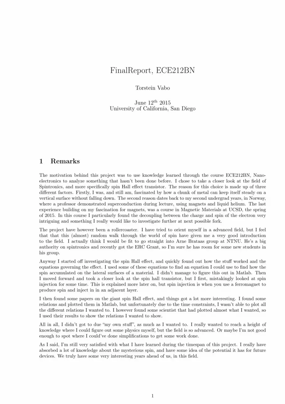
Extrinsic spin Hall effect
The extrinsic spin Hall effect is a subtlety that is good to have knowledge off. It is adequately explained inFig. (5) and accompanying figure text.
Page 5
Torstein Vabo
Figure 5: When an electron is incident on a charged impurity, which way it deviates will depend on the spindirection of the electron. This is because the magnetic field from the electron will interact with the chargeand dependent on field direction it will go either way.
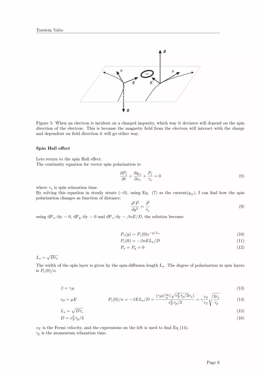
Spin Hall effect
Lets return to the spin Hall effect.The continuity equation for vector spin polarization is:
∂Pj∂t
+∂qij∂xi
+Pjτs
= 0 (8)
where τs is spin relaxation time.By solving this equation in steady steate (=0), using Eq. (7) as the current(qij), I can find how the spinpolarization changes as function of distance:
d2 ~P
dy2=
~P
τs(9)
using dPx/dy = 0, dPy/dy = 0 and dPz/dy = βnE/D, the solution become:
Pz(y) = Pz(0)e−y/Ls (10)Pz(0) = −βnELs/D (11)Px = Py = 0 (12)
Ls =√Dτs
The width of the spin layer is given by the spin-diffusion length Ls. The degree of polarization in spin layersis Pz(0)/n
β = γµ (13)
vd = µE Pz(0)/n = −βELs/D =(γµ) vdµ (
√v2F τp/3τs)
v2F τp/3= γ
vdvf
√3τsτp
(14)
Ls =√Dτs (15)
D = v2F τp/3 (16)
vF is the Fermi velocity, and the expressions on the left is used to find Eq (14).τp is the momentum relaxation time.
Page 6

Torstein Vabo
Giant Spin Hall Effect
The GSHE is the same as the same as spin Hall effect, only that it is very strong. It occurs in high-Z materials,such as platinum, β-tantalum and β-tungsten. The reason it is so much stronger is the stronger spin-orbitcoupling in these materials, which I mentioned earlier in this text. Fig (6) shows a device utilizing this effect.It is composed of a free layer ferromagnet on top of the GSHE metal. The magnetic tunneling junction stackis composed of a free layer ferromagnet, a MgO tunneling oxide and a fixed (pinned) layer of ferromagnet.Then on top of this is a synthetic antiferromagnet and an antiferromagnet placed. The electrodes attachedto the high-Z material is highly conducting to minimize resistance.
Figure 6: Geometry of a 3-terminal memory cell with a spin Hall effect-induced write mechanism and magnetictunneling junction based readout. Dependent of current direction in the bottom material, the free magneticlayer can be written to “1” og “0”.
The transverse spin current, Is, with spin direction σ̂, for a charge current is:
~Is = PSHE(w, t, λsf , θSHE)(σ̂ × ~Ic) (17)
So the spin current is proportional to PSHE which is the spin Hall injection efficiency(SHIE). This efficiencyis given by:
PSHE =~I↑ − ~I~I↑ + ~I
(18)
=πw
4tθSHE
(1− sech
(t
λsf
))(19)
w is the width of the magnet, t is the thickness of the GSHE metal, λsf is the spin flip length, and the angleθSHE is the SHE angle for the GSHE metal to the FM1 interface. The SHIE can reach values of above 100%. The SHIE as function of GSHE metal thickness is shown in Fig (7), where you can see that the optimalthickness is about 2-3 nm.
Page 7

Torstein Vabo
Thickness of Spin Hall Metal, nm ×10-8
0 0.1 0.2 0.3 0.4 0.5 0.6 0.7 0.8 0.9 1
Sp
in P
ola
riza
tio
n R
ato
0
0.2
0.4
0.6
0.8
1
1.2
1.4
1.6
1.8
2
TungstenTantalumPlatinum
Figure 7
Further I found how the required energy to switch the magnetization as function of the energy delay develops.This is where I would really wish I had more time to investigate the different parameters. I would have beenable to find how the different contribution effected the energy, and could have deduced some relations andshown them using e.g. Matlab. Instead I had to use the results I found in [3], and also use their plots.
The equation governing the energy for in-plane switching:
E(τ) = RwriteI2co
(τ + τ0ln
(π2θ0
))2τ
=4
h̄2RwriteP 2
1
τ
(µ0eαMsV
(Hk +
Ms
2
)(τ + τ0ln
( π2θ
)))2
(20)
And the corresponding equation for perpendicular magnetic anisotropy:
E(τ) = RwriteI2co
(τ + τ0ln
(π2θ0
))2τ
=4
h̄2RwriteP 2
1
τ
(µ0eαMsV Hk
(τ + τ0ln
( π2θ
)))2(21)
Rwrite is write resistance of deviceIc is the critical current for spin-transfer torque induces switching.τ0 is characteristic timeτ is the switching time.θSHE is the SHE angle between the GSHE metal and the FM1 layer.P is spin current polarizationMs is magnetization saturationHk anisotropy.V is the volume of the free magnetic layer.
The two equation are plotted in Fig. (8) and Fig. (9). The plots also includes comparison to other devicessuch as perpendicular-to-plane and in-plane spin transfer torque magnetic tunneling junctions.
Page 8

Torstein Vabo
Figure 8: Energy-delay trajectory for in-plane ferromagnet switching. GSHE tungsten, platinum and tantalumcompared to parallel -> anti-parallel and anti-parallel -> parallel switching by “conventional”STT.
Figure 9: Energy-delay trajectory for PMA ferromagnet switching. GSHE tungsten, platinum and tantalumcompared to parallel -> anti-parallel and anti-parallel -> parallel switching,by “conventional”STT.
The plots show that in-plane magnetization GSHE-MTJ devices enables us to obtain switching times asshort as 20 ps or switching energies as small as 2fJ. The PMA-GSHE-MTJ device compared with that of thePMA-STT-MTJ device is reduced to 100 aJ/bit from 100 fJ/bit, an order of magnitude of 3 improvement(!).Alternatively, PMA-GSHE-MTJ devices can be used to reduce the switching time to 10 ps.
It is evidently no doubt about the potential of these effects, concepts and devices, and as mentioned initially,the years to come will be very interesting.
Page 9

Torstein Vabo
references
1. S. Manipatruni et al. “Energy-delay performance of giant spin Hall effect switching for dense magneticmemory”, Applied Physics Express 7, 103001 (2014)
2. Dyakonov, M. I. Spin Physics in Semiconductors. Berlin: Springer, 2008.
3. Jorg Wunderlich et al, “Spin Hall Effect Transistor”, Science 330, 2010, 10.1126/science.1195816.
4. S. Maekawa, “A flood of Spin currents”, Nat. Mat 8, 777-778 (2009).
5. Y. Zhang et. al. “Giant Spin Hall Effect (GSHE) Logic Design for Low Power Application", 978-3-9815370-4-8/DATE15/c 2015 EDAA
6. C.F Pai et al., “Spin transfer torque devices utilizing the giant spin Hall effect of tungsten", AppliedPhysics Letters 101, 122404 (2012).
Page 10