ga-586atv rev. 4
TRANSCRIPT
GA - 586ATV
¡ ]REV. 4¡ ^
USER'S MANUAL
PCI - ISA SOLUTION
Pentium Processor PCI - ISA BUS MAINBOARD
REV. 4 First Edition
GA-586ATV
2
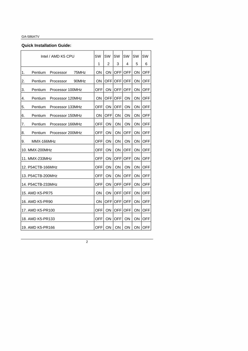
Quick Installation Guide:
Intel / AMD K5 CPU SW
1
SW
2
SW
3
SW
4
SW
5
SW
6
1. Pentium Processor 75MHz ON ON OFF OFF ON OFF
2. Pentium Processor 90MHz ON OFF OFF OFF ON OFF
3. Pentium Processor 100MHz OFF ON OFF OFF ON OFF
4. Pentium Processor 120MHz ON OFF OFF ON ON OFF
5. Pentium Processor 133MHz OFF ON OFF ON ON OFF
6. Pentium Processor 150MHz ON OFF ON ON ON OFF
7. Pentium Processor 166MHz OFF ON ON ON ON OFF
8. Pentium Processor 200MHz OFF ON ON OFF ON OFF
9. MMX-166MHz OFF ON ON ON ON OFF
10. MMX-200MHz OFF ON ON OFF ON OFF
11. MMX-233MHz OFF ON OFF OFF ON OFF
12. P54CTB-166MHz OFF ON ON ON ON OFF
13. P54CTB-200MHz OFF ON ON OFF ON OFF
14. P54CTB-233MHz OFF ON OFF OFF ON OFF
15. AMD K5-PR75 ON ON OFF OFF ON OFF
16. AMD K5-PR90 ON OFF OFF OFF ON OFF
17. AMD K5-PR100 OFF ON OFF OFF ON OFF
18. AMD K5-PR133 OFF ON OFF ON ON OFF
19. AMD K5-PR166 OFF ON ON ON ON OFF
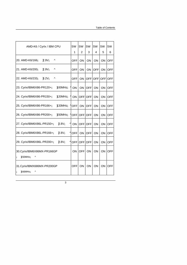
Table of Contents
3
AMD-K6 / CyrIx / IBM CPU SW
1
SW
2
SW
3
SW
4
SW
5
SW
6
20. AMD-K6/166¡ ]2.9V¡ ^ OFF ON ON ON ON OFF
21. AMD-K6/200¡ ]2.9V¡ ^ OFF ON ON OFF ON OFF
22. AMD-K6/233¡ ]3.2V¡ ^ OFF ON OFF OFF OFF OFF
23. Cyrix/IBM6X86-PR120+¡ ]100MHz¡^ ON ON OFF ON ON OFF
24. Cyrix/IBM6X86-PR150+¡ ]120MHz¡^ ON OFF OFF ON ON OFF
25. Cyrix/IBM6X86-PR166+¡ ]133MHz¡^ OFF ON OFF ON ON OFF
26. Cyrix/IBM6X86-PR200+¡ ]150MHz¡^ OFF OFF OFF ON ON OFF
27. Cyrix/IBM6X86L-PR150+¡ ]2.8V¡ ^ ON OFF OFF ON ON OFF
28. Cyrix/IBM6X86L-PR166+¡ ]2.8V¡ ^ OFF ON OFF ON ON OFF
29. Cyrix/IBM6X86L-PR200+¡ ]2.8V¡ ^ OFF OFF OFF ON ON OFF
30.Cyrix/IBM6X86MX-PR166GP
¡ ]150MHz¡ ^
ON OFF ON ON ON OFF
31.Cyrix/IBMX686MX-PR200GP
¡ ]166MHz¡ ^
OFF ON ON ON ON OFF
GA-586ATV
4
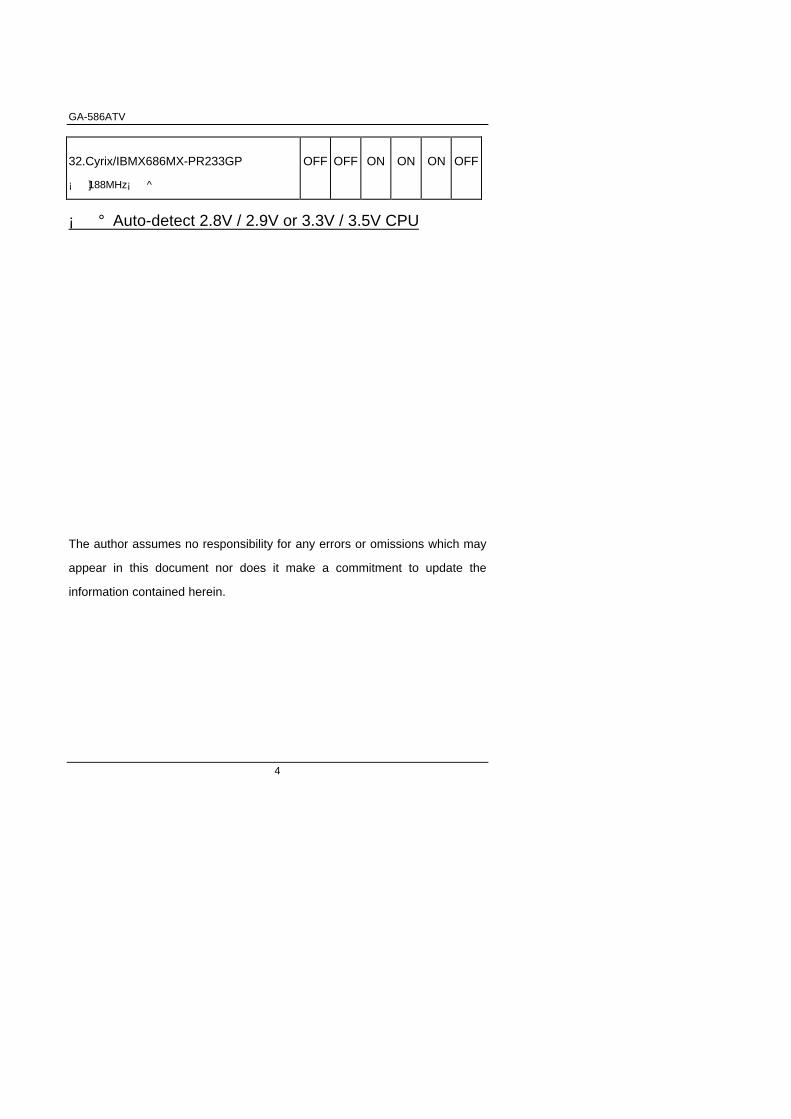
32.Cyrix/IBMX686MX-PR233GP
¡ ]188MHz¡ ^
OFF OFF ON ON ON OFF
¡ ° Auto-detect 2.8V / 2.9V or 3.3V / 3.5V CPU
The author assumes no responsibility for any errors or omissions which may
appear in this document nor does it make a commitment to update the
information contained herein.
Table of Contents
5
Third-party brands and names are the property of their respective owners.
JULY 01, 1997 TAIPEI, TAIWAN
TABLE OF CONTENTS
1. INTRODUCTION................................................................................... 1-1
1.1. PREFACE ............................................................................................................. 1-1
1.2. KEY FEATURES................................................................................................... 1-1
1.3. PERFORMANCE LIST ......................................................................................... 1-2
1.4. BLOCK DIAGRAM................................................................................................ 1-3
1.5. INTRODUCE THE PCI - BUS .............................................................................. 1-4
1.6. FEATURES........................................................................................................... 1-4
2. SPECIFICATION .................................................................................. 2-1
2.1. HARDWARE......................................................................................................... 2-1
2.2. SOFTWARE ......................................................................................................... 2-2
2.3. ENVIRONMENT ................................................................................................... 2-2
3. HARDWARE INSTALLATION .............................................................. 3-1
3.1. UNPACKING......................................................................................................... 3-1
3.2. MAINBOARD LAYOUT (REV.3 AND ABOVE) ........................................................ 3-2
3.3. QUICK REFERENCE FOR JUMPERS & CONNECTORS ................................. 3-2
3.4. DRAM INSTALLATION......................................................................................... 3-5
3.5. SRAM INSTALLATION......................................................................................... 3-6
3.5.1 Onboard Sync. SRAM (Pipe Line Burst SRAM)............................................ 3-6
3.6. CPU INSTALLATION AND JUMPERS SETUP................................................... 3-6
3.7. CMOS RTC & ISA CFG CMOS SRAM ................................................................ 3-6
3.8. SPEAKER CONNECTOR INSTALLATION ......................................................... 3-7
3.9. POWER LED & KEY LOCK CONNECTOR INSTALLATION ............................. 3-7
GA-586ATV
6
3.10. TURBO SWITCH CONNECTOR INSTALLATION............................................ 3-7
3.11. TURBO LED CONNECTOR INSTALLATION ................................................... 3-7
3.12. HARDWARE RESET SWITCH CONNECTOR INSTALLATION ..................... 3-7
3.13. GREEN FUNCTION INSTALLATION ................................................................ 3-8
3.14. PERIPHERAL DEVICE INSTALLATION ........................................................... 3-8
3.15. KEYBOARD SETTING FUNCTION................................................................... 3-8
4. BIOS CONFIGURATION ...................................................................... 4-1
4.1. ENTERING SETUP .............................................................................................. 4-1
4.2. CONTROL KEYS.................................................................................................. 4-2
4.3. GETTING HELP ................................................................................................... 4-3
4.3.1. Main Menu4 .................................................................................................. 4-3
4.3.2. Status Page Setup Menu / Option Page Setup Menu .................................. 4-3
4.4. THE MAIN MENU ................................................................................................. 4-3
4.5. STANDARD CMOS SETUP MENU ..................................................................... 4-5
4.6. BIOS FEATURES SETUP.................................................................................... 4-9
4.7. CHIPSET FEATURES SETUP........................................................................... 4-13
4.8. POWER MANAGEMENT SETUP...................................................................... 4-14
4.9. PNP/PCI CONFIGURATION.............................................................................. 4-16
4.10. INTEGRATED PERIPHERALS........................................................................ 4-17
4.11. LOAD SETUP DEFAULTS............................................................................... 4-21
4.12. USER PASSWORD.......................................................................................... 4-22
4.13. IDE HDD AUTO DETECTION.......................................................................... 4-23
4.14. SAVE & EXIT SETUP....................................................................................... 4-24
4.15. EXIT WITHOUT SAVING................................................................................. 4-25
5. AT TECHNICAL INFORMATION.......................................................... 5-1
5.1. I/O BUS CONNECTOR PIN OUT ........................................................................ 5-1
5.1.1. ISA SLOT PIN OUT...................................................................................... 5-1
5.1.2. PCI - BUS SLOT PIN OUT........................................................................... 5-2
5.2. I/O & MEMORY MAP............................................................................................ 5-3
5.3. TIMER & DMA CHANNELS MAP......................................................................... 5-3
5.4. INTERRUPT MAP ................................................................................................ 5-4

Table of Contents
7
5.5. RTC & CMOS RAM MAP ..................................................................................... 5-5
APPENDIX A: POST MESSAGE..............................................................A-1
APPENDIX B: POST CODES...................................................................B-1
APPENDIX C: BIOS DEFAULT DRIVE TABLE ........................................C-1
APPENDIX D: PROBLEM SHEET............................................................D-1
APPENDIX E: FCC DOCUMENT ............................................................. E-1

Introduction
1-1
1. INTRODUCTION
1.1. PREFACE
Welcome to use the GA - 586ATV motherboard. The motherboard is a 512
KB CACHE Pentium Processor based PC / AT compatible system with ISAbus and PCI Local Bus, and has been designed to be the fastest PC / ATsystem. There are some new features allow you to operate the system withjust the performance you want.
This manual also explains how to install the motherboard for operation, andhow to set up your CMOS CONFIGURATION with BIOS SETUP program.
1.2. KEY FEATURES
q Pentium Processor based PC / AT compatible mainboard.
q Supports 321 Pins (Socket 7) ZIF white socket on board.
q Auto detect 3.3V - 3.5V and 2.8V - 2.9V CPU.
q Supports Pentium Processor, running at 75-233 MHz.
q Supports 512 KB Pipeline Burst Sync. 2nd Cache.
q 4 Master / Slave PCI Bus slots, 3 ISA Bus slots.
q Supports 8 - 128 MB DRAM memory on board.
q Supports 2 channels Enhance PCI IDE ports for 4 IDE Device.
q Supports 2xCOM (16550), 1xLPT (EPP / ECP), 1x2.88MB Floppy port.
q USB function is ready for option.
q Supports Green function, Plug & Play function.
q Licensed AWARD BIOS, FLASH EEPROM for BIOS update.
q 2/3 BABY AT size, 4 layers PCB.
GA-586ATV
1-2
1.3. PERFORMANCE LIST
The following performance data list is the testing results of some popularbenchmark testing programs. These data are just referred by users.(The different Hardware & Software configuration will result in differentbenchmark testing results.)
• CPU Pentium processor 233 MHz
• DRAM 32 MB EDO
• CACHE SIZE 512 KB Pipeline Burst SRAM
• DISPLAY Matrox Millennium 2MB
• STORAGE Onboard IDE port + Quantum Fireball 1280AT
• SOUND Creative 32 PnP
• O.S. Windows 95 OSR2
with Display Driver at 1024 x 768 x 256 colors x 75Hz
CPUSoftware
Intel MMX-233 AMD K6-233
Winbench 97
CPU mark32 471 566
Winstone 97
Business
Hi-End
46
20.8
48
20.7
Intel Media
Bench mark 1.0 298.31 247.98
Introduction
1-3
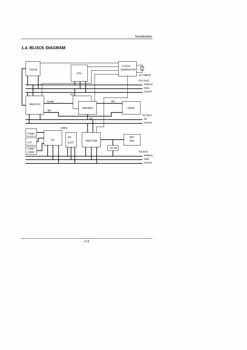
1.4. BLOCK DIAGRAM
CACHE
CPU
CLOCK
GENERATOR
14.718MHZ
S82437VX
HD
DLINK
MA
AD
S82438VX DRAM
Floppy
LPT
COM1COM2
24MHz
I/OISA
SLOTS82371SB
74F245
IDE1
IDE2
CPU BUS
Address
Data
Control
PCI BUS
AD
Control
ISA BUS
Address
Data
Control
MD
GA-586ATV
1-4
1.5. INTRODUCE THE PCI - BUS
Connecting devices to a CPU local bus can dramatically increase the speedof I/O-bound peripherals with only a slight increase in cost over traditionalsystems. This price / performance point has created a vast market potentialfor local bus products. The main barrier to this market has been the lack ofan accepted standard for local bus peripherals. Many mainboard and chipsetmanufactures developed their own local bus implementations, but they areincompatible with each other. The VL (Video Electronics StandardsAssociation) local bus and PCI (Peripheral Component Interconnect) busspecification was created to end this confusion.
The PCI - bus standard, under development since Jun. 1992, which isdesigned to bring workstation-level performance to standard PC platform.The PCI - bus removes many of the bottlenecks that have hampered PC forseveral years. On the PCI - bus, peripherals operate at the native speed ofthe computer system, thus enabling data transfer between peripherals andthe system at maximum speed. This performance is critical for bandwidth-constrained devices such as video, multimedia, mass storage, andnetworking adapters.
PCI - bus standard provides end-users with a low-cost, extendible andportable local bus design, which will allow system and peripherals fromdifferent manufactures to work together.
1.6. FEATURES
q 32 bits bus transfer mode.
q Bus Master or Slave access.
q Memory burst transfer to 132 MB/sec.
q 33 MHz operation speed.
q 10 device loading ability.
q CPU independent.
Specification
2-1
2. SPECIFICATION
2.1. HARDWARE
• CPU − Intel Pentium processor (with MMX) 75 - 233MHz.
− AMDK5, K6 and Cyrix / IBM 6x86.− 321 pins (socket 7) ZIF white socket on board.− Automatically setup 3.3V ~ 3.5V / 2.8V ~ 2.9V for
dual power CPU.• COPROCESSOR − Included in Pentium Processor.• SPEED − 50 / 60 / 66 / 75 MHz system and 25 / 30 / 33 / 37.5
PCI-Bus speed.− Hardware and Software speed switchable function.
• DRAM MEMORY − 2 banks 72 pins SIMM module socket on board.− Use 4 / 8 / 16 / 32 MB 60~70 ns SIMM module
DRAM.− 8 ~ 128 MB DRAM size.− Support Fast Page / EDO DRAM access mode.
• CACHE MEMORY − 16 KB cache memory included in PentiumProcessor .
− 512 KB Pipeline Burst 2nd cache.− Support Write Back cache function for both CPU &
on board cache.• SHADOW RAM − Main BIOS shadow function.
− Video BIOS shadow function programmable.− Shadow RAM cacheable function.
• I/O BUS SLOTS − 4 Master / Slave PCI-BUS.− 3 16 bits ISA BUS.
• USB PORTS − Optional extended cable for dual USB port.• IDE PORTS − 2 Enhanced IDE channels on board.(Using
IRQ14,15)− Support Mode 3,4 IDE & ATAPI CD - ROM.
• I/O PORTS − Supports 2*16550 COM ports. (Using IRQ4, 3)− Supports 1*EPP/ECP LPT port. (Using IRQ7 or 5
and DMA3 or 1)− Supports 1*2.88MB Floppy port. (Using DMA2 &
IRQ6)− Supports PS/2 Mouse. (Using IRQ12 )
GA-586ATV
2-2
− USB function optional.• GREEN FUNCTION − Standby & Suspend mode support.
− Green switch & LED support.− IDE & Display power down support.− Monitor all IRQ / DMA / Display / I/O events.
• BIOS − 128KB FLASH EEPROM.− Supports Plug & Play Function.
• DIMENSION − 2/3Baby AT size / 4 layers.
2.2. SOFTWARE
• BIOS − Licensed AWARD BIOS.− AT CMOS Setup, BIOS / Chipset Setup, Green
Setup, Hard Disk Utility included.• O.S. − Operation with MS-DOS, Windows/95,
WINDOWS NT, OS/2, NOVELL and SCOUNIX.
2.3. ENVIRONMENT
• Ambient Temp. − 0°C to +45°C (Operating).• Relative Hum. − 0 to +85% (Operating).• Altitude − 0 to 10,000 feet (Operating).• Vibration − 0 to 1,000 Hz.• Electricity − 4.9 V to 5.2 V.
− 10 A to 15 A current.
Hardware Installation
3-1
3. HARDWARE INSTALLATION
3.1. UNPACKING
The mainboard package should contain the following:
• The GA - 586ATV mainboard.
• USER'S MANUAL.
• Cable set for I/O Device.
• Diskette for BUS MASTER IDE Driver.
The mainboard contains sensitive electric components which can be easilydamaged by static electricity, so the mainboard should be left in its originalpacking until it is installed.
Unpacking and installation should be done on a grounded anti-static mat.The operator should be wearing an anti static wristband, grounded at thesame point as the anti-static mat.
Inspect the mainboard carton for obvious damage. Shipping and handlingmay cause damage to your board. Be sure there are no shipping andhandling damages on the board before proceeding.
After opening the mainboard carton, extract the system board and place itonly on a grounded anti-static surface component side up. Again inspect theboard for damage. Press down on all of the socket IC's to make sure thatthey are properly seated. Do this only on with the board placed on a firm flatsurface.
MDO NOT APPLY POWER TO THE BOARD IF IT HAS BEEN DAMAGED.
You are now ready to install your mainboard. The mounting hole pattern onthe mainboard matches the IBM-AT system board. It is assumed that thechassis is designed for a standard IBM XT/AT mainboard mounting.
Place the chassis on the anti-static mat and remove the cover. Take theplastic clips, Nylon stand-off and screws for mounting the system board, andkeep them separate.
GA-586ATV
3-2
3.2. MAINBOARD LAYOUT (REV.3 and above)
++
J7
J6
J12
J11
J10 J8
J9
RTCBIOS
+
J5
CPU
+
J4
ISA SLOT3
ISA SLOT2
ISA SLOT1
PCI4
PCI3
PCI2
PCI1
IDE2
IDE1 LPT PORT
SIMM1
SIMM4
COMB
COMA
GA-586ATV
1
1
1CN3
CN2
1
PS/2 MOUSE
J2
Keyboard
J1
Power1
CN6
CN4
CN1
123456
S1
CN7FLOPPY82438VXSYNC
SRAM
SYNC
SRAM
U10
USBJ3
1
2
1
2
2
1
14
1
82438VX
×Figure 3.1Ø
3.3. QUICK REFERENCE FOR JUMPERS & CONNECTORS
t J1: Keyboard ConnectorPin No. Function
1 Key Clock.2 Key Data.3 NC.4 VCC (+5V).5 GND.
Hardware Installation
3-3
t J2: PS/2 Mouse ConnectorPin No. Function
1 VCC.2 GND.3 MS-DATA.4 MS-CLOCK.
t J4: IDE Hard Disk Active LEDPin No. Function
1 LED anode (+).2 LED cathode (-).
t J5: CPU Cooling Fan Power ConnectorPin No. Function
1 +12V2 GND
t J6: Speaker ConnectorPin No. Function
1 VCC.2 NC.3 NC.4 Data.
t J7: Power LED and Key-Lock ConnectorPin No. Function
1 LED anode (+).2 NC.3 LED cathode (-).4 Key lock.5 GND.
t J8: Green Function SwitchPin No. FunctionClose For system entering Green mode ( Suspend mode).Open Normal operation.
t J9: Green Function LEDPin No. Function
1 LED anode (+).2 LED cathode (-).
t J10: Reset Switch
GA-586ATV
3-4
Open For normal operation.Close For hardware reset system.
t J11: Turbo SwitchPin No. FunctionClose For low speed (Non-cache).Open For high speed.
t J12: Turbo LED ConnectorPin No. Function
1 LED anode (+).2 LED cathode (-).
t S1-1,2: CPU BUS CLOCKMHz 1 275 OFF OFF66 OFF ON60 ON OFF50 ON ON
t S1-3,4: CPU INT. / EXT. CLOCK RATIO¡ ]For REV.3x¡ ^
RATIO 3 4x 1.5 or x 3.5 OFF OFF
x 2 OFF ON x 2.5 ON ON
x 3 ON OFF
t S1-3, 4, 6: CPU INT. / EXT. CLOCK RATIO¡ ]For REV.4x¡ ^
RATIO 3 4 6x 1.5 or x 3.5 OFF OFF OFF
x 2 OFF ON OFF x 2.5 ON ON OFF
x 3 ON OFF OFFx 5.5 OFF OFF ONx 4 OFF ON ON
x 4.5 ON ON ONx 5 ON OFF ON
t S1-5: AMD K6 3.2V CPU supportCPU 5
AMD K6 3.2V CPU OFFIntel & Cyrix & AMD K5, K6 (2.9V) ON
t CN1-4,6,7,J3 I/O Ports Connector
Hardware Installation
3-5
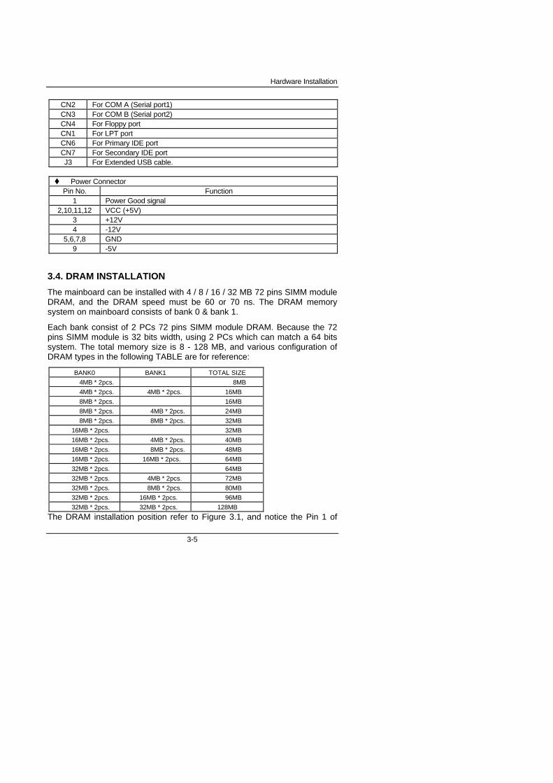
CN2 For COM A (Serial port1)CN3 For COM B (Serial port2)CN4 For Floppy portCN1 For LPT portCN6 For Primary IDE portCN7 For Secondary IDE portJ3 For Extended USB cable.
t Power ConnectorPin No. Function
1 Power Good signal2,10,11,12 VCC (+5V)
3 +12V4 -12V
5,6,7,8 GND9 -5V
3.4. DRAM INSTALLATION
The mainboard can be installed with 4 / 8 / 16 / 32 MB 72 pins SIMM moduleDRAM, and the DRAM speed must be 60 or 70 ns. The DRAM memorysystem on mainboard consists of bank 0 & bank 1.
Each bank consist of 2 PCs 72 pins SIMM module DRAM. Because the 72pins SIMM module is 32 bits width, using 2 PCs which can match a 64 bitssystem. The total memory size is 8 - 128 MB, and various configuration ofDRAM types in the following TABLE are for reference:
BANK0 BANK1 TOTAL SIZE
4MB * 2pcs. 8MB
4MB * 2pcs. 4MB * 2pcs. 16MB
8MB * 2pcs. 16MB
8MB * 2pcs. 4MB * 2pcs. 24MB
8MB * 2pcs. 8MB * 2pcs. 32MB
16MB * 2pcs. 32MB
16MB * 2pcs. 4MB * 2pcs. 40MB
16MB * 2pcs. 8MB * 2pcs. 48MB
16MB * 2pcs. 16MB * 2pcs. 64MB
32MB * 2pcs. 64MB
32MB * 2pcs. 4MB * 2pcs. 72MB
32MB * 2pcs. 8MB * 2pcs. 80MB
32MB * 2pcs. 16MB * 2pcs. 96MB
32MB * 2pcs. 32MB * 2pcs. 128MB
The DRAM installation position refer to Figure 3.1, and notice the Pin 1 of
GA-586ATV
3-6
SIMM module must match with the Pin 1 of SIMM socket when the DRAMSIMM module is installed.
Insert the DRAM SIMM module into the SIMM socket at 45 degree angle. Ifthere is a wrong direction of Pin 1, the DRAM SIMM module couldn't beinserted into socket completely.
After completely insert SIMM module into socket, then press the SIMMmodule in vertical direction until the left and right metal holders can keep theSIMM module standing up con-firmly.
3.5. SRAM INSTALLATION
3.5.1 Onboard Sync. SRAM (Pipe Line Burst SRAM)
Sync SRAM consists of 2 PCs Pipeline Burst 64 K x 32- 6/7 for 512KB Sync.SRAM. The TAG SRAM (U10) is 16KBx8-12.
3.6. CPU INSTALLATION AND JUMPERS SETUP
The system's speed depends on the frequency of CLOCK GENERATOR.The user can change the selection to set up the system speed to 50 MHz, 60MHz, 66 MHz or 75 MHz for Intel 75 - 233 MHz 3.3V ~ 3.5V and 2.8V ~ 2.9Vdual power plane Pentium Processor.
The mainboard can use Intel Pentium Processor (MMX or PODP), Cyrix6x86 and AMD K5 / K6 processor and the CPU speed must match with thefrequency of CLOCK GEN. It will cause system hanging up if the CLOCKGEN.'S frequency is higher than CPU's.
M The CPU is a sensitive electric component and it can be easilydamaged by static electricity, so users must keep it away frommetal surface when the CPU is installed onto mainboard.
M When the user installs the CPU on socket, please notice the PIN 1of CPU is in the same corner as the PIN 1 of socket!
M Before the CPU is installed, the mainboard must be placed on a flatplane in order to avoid being broken by the pressure of CPUinstallation.
3.7. CMOS RTC & ISA CFG CMOS SRAM
Hardware Installation
3-7
There're RTC & CMOS SRAM on board, they have a power supply frominternal battery to keep the DATA inviolate & effective. The RTC is a REAL-TIME CLOCK device which provides the DATE & TIME to system. TheCMOS SRAM is used for keeping the information of ISA device systemconfiguration, so the system can automatically boot OS. every time.
Due to the life-time of 3V Li-battery is 5 years, the user can change a newone to replace old one after it can not work.
3.8. SPEAKER CONNECTOR INSTALLATION
There is always a speaker in AT system for sound purpose. The 4 - Pinsconnector J6 is used to connect speaker.
The speaker can work well in both direction of connector when it is installedto the connector J6 on mainboard.
3.9. POWER LED & KEY LOCK CONNECTOR INSTALLATION
There are a system power LED lamp and a key on the panel of case. Thepower LED will light on when system is powered-on, and the key can lock thekeyboard input or unlock it, both of them are connected to a 5 PIN connector.The connector should be installed to J7 of mainboard in correct direction.
3.10. TURBO SWITCH CONNECTOR INSTALLATION
The TURBO switch on the panel is used for controlling the system speed.Some program developed on XT should be executed with a low speedsystem, so a high speed system needs the speed switching function tochange its running speed.
The mainboard uses 50 MHz speed method to implement DE-TURBOswitching function. The J11 on mainboard should be connected to theTURBO switch on panel, and user can push in or pop out the TURBO switchto enable or disable the turbo function of system.
NOTE: If the system already use 50MHz clock, then the TURBO functionwill inactive.
3.11. TURBO LED CONNECTOR INSTALLATION
The TURBO LED on panel can indicate the current speed status of system.The TURBO LED connector should be installed to J12 in correct direction.3.12. HARDWARE RESET SWITCH CONNECTOR INSTALLATION
GA-586ATV
3-8
The RESET switch on panel provides users with HARDWARE RESETfunction which is almost the same as power-on/off. The system will do a coldstart after the RESET switch is pushed and released by user.
The RESET switch is a 2 PIN connector and should be installed to J10 onmainboard.
3.13. GREEN FUNCTION INSTALLATION
For the purpose of power saving, there are two jumpers, J8 and J9, to makesure the power saving function doing well.
The J9 is a indicator (green LED) for green function. If the green LED is ON,the system is operating in green mode.
The J8 is a switch to force the system get into green mode immediately.
3.14. PERIPHERAL DEVICE INSTALLATION
After the device installation and jumpers setup, the mainboard can bemounted into the case and fixed by screw. To complete the mainboardinstallation, the peripheral device could be installed now. The basic systemneeds a display interface card and a disk device.
If the PCI - Bus device is to be installed in the system, any one of four PCI -Bus slots can be used no matter Slave or Master PCI - Bus device beinginstalled. After installing the peripheral device, the user should checkeverything again, and prepare to power-on the system.
3.15. KEYBOARD SETTING FUNCTION
After booting the O.S., there are some special functions used by keyboard asfollows:
"CTRL_ALT_DEL" − Pressing these keys simultaneously will cause system to Warm Start (Software Reset).
BIOS Configuration
4-1
4. BIOS CONFIGURATION
Award's BIOS ROM has a built-in Setup program that allows users to modifythe basic system configuration. This type of information is stored in battery-backed CMOS SRAM so that it retains the Setup information when the poweris turned off.
4.1. ENTERING SETUP
Power ON the computer and press <Del> immediately will allow you to enterSetup. The other way to enter Setup is to power on the computer, when thebelow message appears briefly at the bottom of the screen during the POST(Power On Self Test), press <Del> key or simultaneouslypress <Ctrl>, <Alt>, and <Esc> keys.
� TO ENTER SETUP BEFORE BOOT PRESS CTRL-ALT-ESC OR DEL KEY
If the message disappears before you respond and you still wish to enterSetup, restart the system to try again by turning it OFF then ON or pressingthe "RESET" bottom on the system case. You may also restart bysimultaneously press <Ctrl>,<Alt>, and <Del> keys.
If you do not press the keys at the correct time and the system does not boot,an error message will be displayed and you will again be asked to,
� PRESS F1 TO CONTINUE, CTRL-ALT-ESC OR DEL TO ENTER SETUP
GA-586ATV
4-2
4.2. CONTROL KEYS
Up arrow Move to previous item
Down arrow Move to next item
Left arrow Move to the item in the left hand
Right arrow Move to the item in the right hand
Esc key Main Menu - Quit and not save changes into CMOSStatus Page Setup Menu and Option Page Setup Menu - Exit currentpage and return to Main Menu
PgUp key Increase the numeric value or make changes
PgDn key Decrease the numeric value or make changes
F1 key General help, only for Status Page Setup Menu and Option PageSetup Menu
F2 key Change color from total 16 colors
F3 key Calendar, only for Status Page Setup Menu
F4 key Reserved
F5 key Restore the previous CMOS value from CMOS, only for Option PageSetup Menu
F6 key Load the default CMOS value from BIOS default table, only for OptionPage Setup Menu
F7 key Load the default
F8 key Reserved
F9 key Reserved
F10 key Save all the CMOS changes, only for Main Menu
BIOS Configuration
4-3
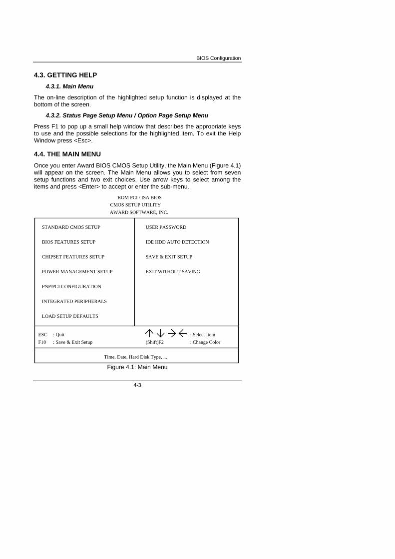
4.3. GETTING HELP
4.3.1. Main Menu
The on-line description of the highlighted setup function is displayed at thebottom of the screen.
4.3.2. Status Page Setup Menu / Option Page Setup Menu
Press F1 to pop up a small help window that describes the appropriate keysto use and the possible selections for the highlighted item. To exit the HelpWindow press <Esc>.
4.4. THE MAIN MENU
Once you enter Award BIOS CMOS Setup Utility, the Main Menu (Figure 4.1)will appear on the screen. The Main Menu allows you to select from sevensetup functions and two exit choices. Use arrow keys to select among theitems and press <Enter> to accept or enter the sub-menu.
ROM PCI / ISA BIOS
CMOS SETUP UTILITY
AWARD SOFTWARE, INC.
STANDARD CMOS SETUP
BIOS FEATURES SETUP
CHIPSET FEATURES SETUP
PNP/PCI CONFIGURATION
LOAD SETUP DEFAULTS
USER PASSWORD
IDE HDD AUTO DETECTION
SAVE & EXIT SETUP
EXIT WITHOUT SAVING
ESC
F10
: Quit
: Save & Exit Setup (Shift)F2
: Select Item
: Change Color
Time, Date, Hard Disk Type, ...
POWER MANAGEMENT SETUP
INTEGRATED PERIPHERALS
Figure 4.1: Main Menu
GA-586ATV
4-4
• Standard CMOS setup
This setup page includes all the items in a standard compatible BIOS.
• BIOS features setup
This setup page includes all the items of Award special enhancedfeatures.
• Chipset features setup
This setup page includes all the items of chipset special features.
• Power management setup
This setup page includes all the items of Green function features.
• PNP/PCI configuration
This setup page includes all the configurations of PCI & PNP ISAresources.
• Integrated peripherals
This setup page includes all onboard peripherals.
• Load setup defaults
BIOS defaults indicates the most appropriate value of the systemparameter which the system would be in safe configuration.
• User password
Change, set, or disable password. It allows you to limit access to thesystem and Setup, or just to Setup.
• IDE HDD auto detection
Automatically configure hard disk parameter.
• Save & exit setup
Save CMOS value changes to CMOS and exit setup.
• Exit without save
Abandon all CMOS value changes and exit setup.
BIOS Configuration
4-5
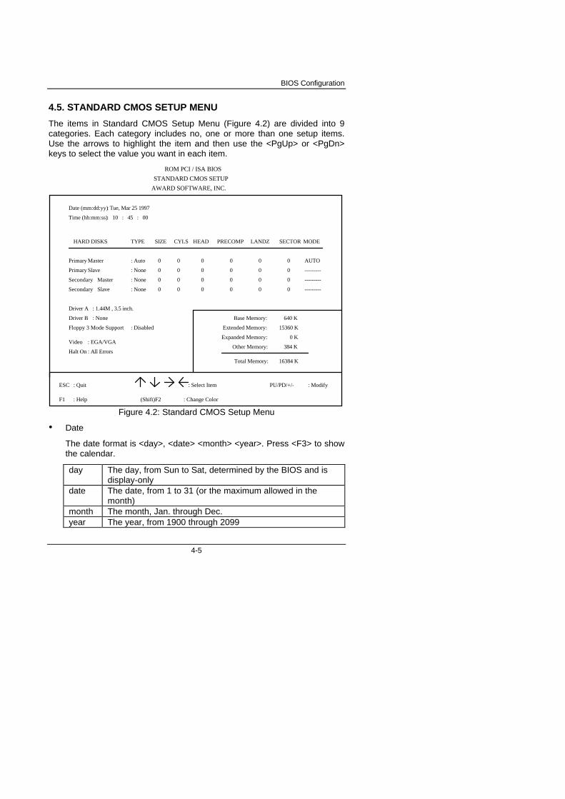
4.5. STANDARD CMOS SETUP MENU
The items in Standard CMOS Setup Menu (Figure 4.2) are divided into 9categories. Each category includes no, one or more than one setup items.Use the arrows to highlight the item and then use the <PgUp> or <PgDn>keys to select the value you want in each item.
ROM PCI / ISA BIOS
STANDARD CMOS SETUP
AWARD SOFTWARE, INC.
ESC
F1
: Quit
: Help (Shift)F2
: Select Item
: Change Color
Date (mm:dd:yy)
Time (hh:mm:ss)
Master
Video
Halt On : All Errors
: EGA/VGA
: None
Slave
HEAD PRECOMP LANDZ SECTOR
0000 0
Base Memory:
Other Memory:
Expanded Memory:
Extended Memory:
Total Memory:
15360 K
640 K
0 K
384 K
16384 K
PU/PD/+/- : Modify
: Tue, Mar 25 1997
: 10 : 45 : 00
Primary
Secondary Master
Slave
0000 0
0000 0
000 0
Primary
Secondary
: Auto
CYLSHARD DISKS TYPE MODE
0
---------
SIZE
0
0
0
0
Driver A
Driver B
: 1.44M , 3.5 inch.
: None
AUTO
Floppy 3 Mode Support : Disabled
: None
: None
---------
---------
Figure 4.2: Standard CMOS Setup Menu
• Date
The date format is <day>, <date> <month> <year>. Press <F3> to showthe calendar.
day The day, from Sun to Sat, determined by the BIOS and isdisplay-only
date The date, from 1 to 31 (or the maximum allowed in themonth)
month The month, Jan. through Dec.year The year, from 1900 through 2099
GA-586ATV
4-6
• Time
The time format in <hour> <minute> <second>. The time is calculatedbase on the 24-hour military-time clock. For example, 1 p.m. is13:00:00.
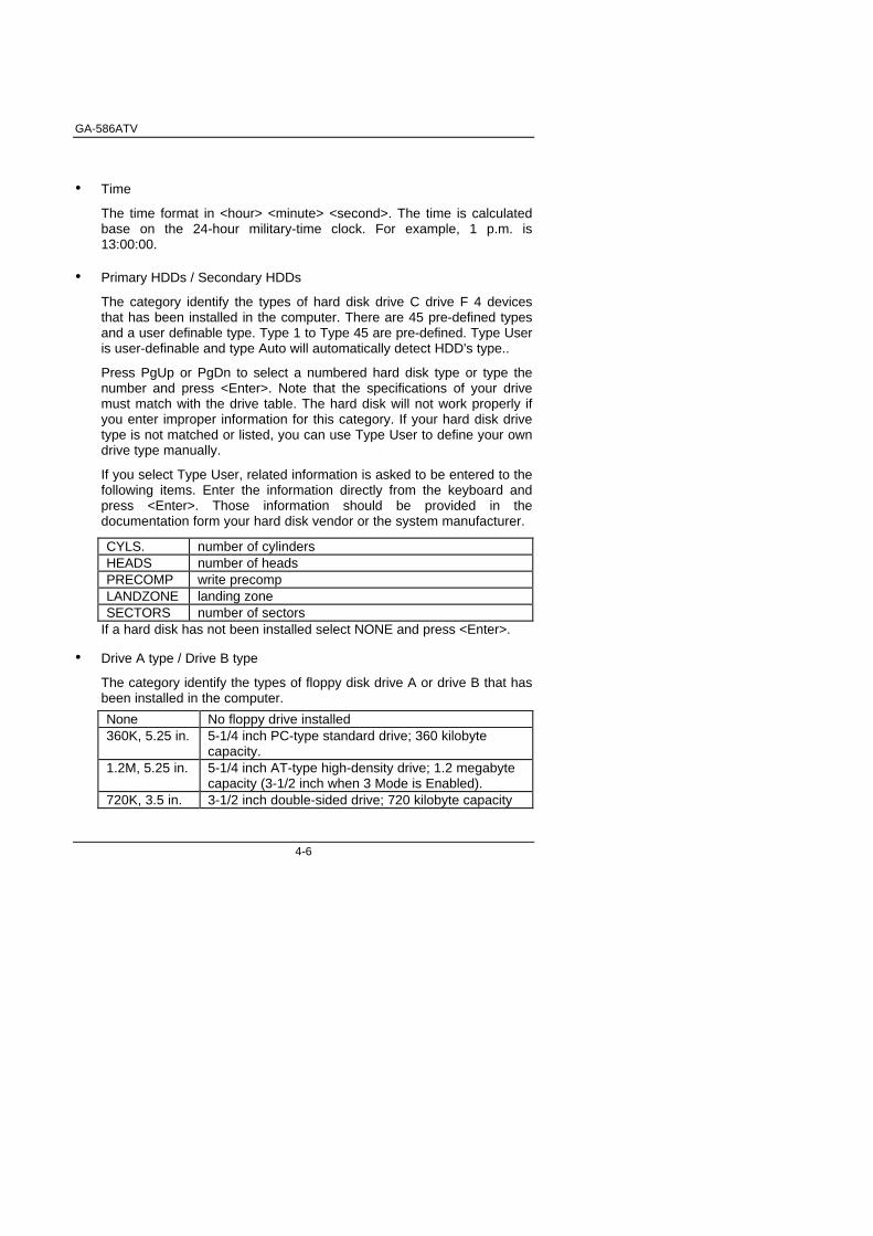
• Primary HDDs / Secondary HDDs
The category identify the types of hard disk drive C drive F 4 devicesthat has been installed in the computer. There are 45 pre-defined typesand a user definable type. Type 1 to Type 45 are pre-defined. Type Useris user-definable and type Auto will automatically detect HDD's type..
Press PgUp or PgDn to select a numbered hard disk type or type thenumber and press <Enter>. Note that the specifications of your drivemust match with the drive table. The hard disk will not work properly ifyou enter improper information for this category. If your hard disk drivetype is not matched or listed, you can use Type User to define your owndrive type manually.
If you select Type User, related information is asked to be entered to thefollowing items. Enter the information directly from the keyboard andpress <Enter>. Those information should be provided in thedocumentation form your hard disk vendor or the system manufacturer.
CYLS. number of cylindersHEADS number of headsPRECOMP write precompLANDZONE landing zoneSECTORS number of sectors
If a hard disk has not been installed select NONE and press <Enter>.
• Drive A type / Drive B type
The category identify the types of floppy disk drive A or drive B that hasbeen installed in the computer.
None No floppy drive installed360K, 5.25 in. 5-1/4 inch PC-type standard drive; 360 kilobyte
capacity.1.2M, 5.25 in. 5-1/4 inch AT-type high-density drive; 1.2 megabyte
capacity (3-1/2 inch when 3 Mode is Enabled).720K, 3.5 in. 3-1/2 inch double-sided drive; 720 kilobyte capacity
BIOS Configuration
4-7
1.44M, 3.5 in. 3-1/2 inch double-sided drive; 1.44 megabytecapacity.
• Floppy 3 Mode Support (for Japan Area)
Disable Normal Floppy Drive.Drive A Drive A is 3 mode Floppy Drive.Drive B Drive B is 3 mode Floppy Drive.Both Drive A & B are 3 mode Floppy Drive.
• Video
The category detects the type of adapter used for the primary systemmonitor that must matches your video display card and monitor.Although secondary monitors are supported, you do not have to selectthe type in setup.
EGA/VGA Enhanced Graphics Adapter/Video Graphics Array. ForEGA, VGA, SVGA, or PGA monitor adapters
CGA 40 Color Graphics Adapter, power up in 40 column mode
CGA 80 Color Graphics Adapter, power up in 80 column mode
MONO Monochrome adapter, includes high resolutionmonochrome adapters
• Halt on
The category determines whether the computer will stop if an error isdetected during power up.
NO errors The system boot will not be stopped for any errorthat may be detected
All errors Whenever the BIOS detects a non-fatal error thesystem will be stopped and you will be prompted
All, But Keyboard The system boot will not stop for a keyboarderror; it will stop for all other errors
All, But Diskette The system boot will not stop for a disk error; itwill stop for all other errors
All, But Disk/Key The system boot will not stop for a keyboard or
GA-586ATV
4-8
disk error; it will stop for all other errors
• Memory
The category is display-only which is determined by POST (Power OnSelf Test) of the BIOS.
Base Memory
The POST of the BIOS will determine the amount of base (orconventional) memory installed in the system. The value of thebase memory is typically 512 K for systems with 512 K memoryinstalled on the motherboard, or 640 K for systems with 640 Kor more memory installed on the motherboard.
Extended Memory
The BIOS determines how much extended memory is presentduring the POST. This is the amount of memory located above1 MB in the CPU's memory address map.
Expanded Memory
Expanded Memory in memory defined by theLotus/Intel/Microsoft (LIM) standard as EMS. Many standardDOS applications can not utilize memory above 640 K, theExpanded Memory Specification (EMS) swaps memory whichnot utilized by DOS with a section, or frame, so theseapplications can access all of the system memory.
Memory can be swapped by EMS is usually 64 K within 1 MBor memory above 1 MB, depends on the chipset design.
Expanded memory device driver is required to use memory asExpanded Memory.
Other Memory
This refers to the memory located in the 640 K to 1024 Kaddress space. This is memory that can be used for differentapplications. DOS uses this area to load device drivers to keep
BIOS Configuration
4-9
as much base memory free for application programs. Most usefor this area is Shadow RAM.
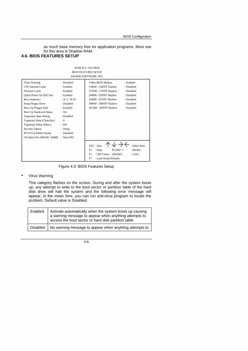
4.6. BIOS FEATURES SETUP
ROM PCI / ISA BIOS
BIOS FEATURES SETUP
AWARD SOFTWARE, INC.
: Select Item
Virus Warning
CPU Internal Cache
External Cache
Boot Sequence
Boot Up Floppy Seek
Boot Up NumLock Status
Security Option
Video BIOS Shadow
C8000 - CBFFF Shadow
: On
: Enabled
: Enabled
: Enabled
: Enabled
: A, C, SCSI
: Setup
: Enabled
: Disabled
ESC
F1
F5
F7 : Load Setup Defaults
: Quit
: Help
: Old Values
PU/PD/+/-
(Shift)F2
: Modify
: Color
Quick Power On Self Test
: Disabled
Swap Floppy Drive : Disabled
: DisabledD0000 - D3FFF Shadow
: DisabledD8000 - DBFFF Shadow
CC000 - CFFFF Shadow : Disabled
: DisabledD4000 - D7FFF Shadow
: DisabledDC000 - DFFFF Shadow
PCI/VGA Palette Snoop : Disabled
Typematic Rate Setting
Typematic Rate (Chars/Sec)
Typematic Delay (Msec)
: Disabled
: 6
:250
OS Select For DRAM >64MB : Non-OS2
Figure 4.3: BIOS Features Setup
• Virus Warning
This category flashes on the screen. During and after the system bootsup, any attempt to write to the boot sector or partition table of the harddisk drive will halt the system and the following error message willappear, in the mean time, you can run anti-virus program to locate theproblem. Default value is Disabled.
Enabled Activate automatically when the system boots up causinga warning message to appear when anything attempts toaccess the boot sector or hard disk partition table
Disabled No warning message to appear when anything attempts to
GA-586ATV
4-10
access the boot sector or hard disk partition table
• CPU Internal Cache / External Cache
These two categories speed up memory access. However, it depends onCPU / chipset design. The default value is Enabled.
Enabled Enable cacheDisabled Disable cache
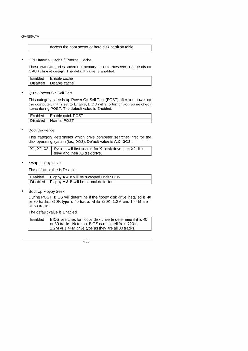
• Quick Power On Self Test
This category speeds up Power On Self Test (POST) after you power onthe computer. If it is set to Enable, BIOS will shorten or skip some checkitems during POST. The default value is Enabled.
Enabled Enable quick POSTDisabled Normal POST
• Boot Sequence
This category determines which drive computer searches first for thedisk operating system (i.e., DOS). Default value is A,C, SCSI.
X1, X2, X3 System will first search for X1 disk drive then X2 diskdrive and then X3 disk drive.
• Swap Floppy Drive
The default value is Disabled.
Enabled Floppy A & B will be swapped under DOSDisabled Floppy A & B will be normal definition
• Boot Up Floppy Seek
During POST, BIOS will determine if the floppy disk drive installed is 40or 80 tracks. 360 K type is 40 tracks while 720 K, 1.2 M and 1.44 M areall 80 tracks.
The default value is Enabled.
Enabled BIOS searches for floppy disk drive to determine if it is 40or 80 tracks, Note that BIOS can not tell from 720 K,1.2 M or 1.44 M drive type as they are all 80 tracks
BIOS Configuration
4-11
Disabled BIOS will not search for the type of floppy disk drive bytrack number. Note that there will not be any warningmessage if the drive installed is 360 K
• Boot Up NumLock Status
The default value is On.
On Keypad is number keysOff Keypad is arrow keys
• Typematic Rate Setting
The default value is Disabled.
Enabled Enable Keyboard typematic rate setting.Disabled Disable Keyboard typematic rate setting.
• Typematic Rate (Chars/Sec)
The default value is 6.
6-30 Set the maximum typematic rate from 6 chars. per secondto 30 chars. per second.
• Typematic Delay (mSec)
The default value is 250.
250-1000 Set the time delay from first key to repeat the same keyin to computer.
• Security Option
This category allows you to limit access to the system and Setup, or justto Setup. The default value is Setup.
System The system will not boot and access to Setup will bedenied if the correct password is not entered at the prompt
Setup The system will boot, but access to Setup will be denied ifthe correct password is not entered at the prompt
M To disable security, select PASSWORD SETTING at Main Menu andthen you will be asked to enter password. Do not type anything and
GA-586ATV
4-12
just press <Enter>, it will disable security. Once the security isdisabled, the system will boot and you can enter Setup freely.
• OS Select For DRAM>64MB
The default value is Non-OS2.
Non-OS2 Using non-OS2 operating system.OS2 Using OS2 operating system and DRAM>64MB.
• Video BIOS Shadow
It determines whether video BIOS will copied to RAM, however, it isoptional from chipset design. Video Shadow will increase the videospeed.
The default value is Enable.
Enabled Video shadow is enabledDisabled Video shadow is disabled
• C8000 - CFFFF Shadow / D0000 - DFFFF Shadow
These categories determine whether optional ROM will be copied toRAM by 16 K byte.
The default value are Disabled.
Enabled Optional shadow is enabledDisabled Optional shadow is disabled
• PCI/VGA Palette Snoop
The default value are Disabled.
Enabled For having Video Card on ISA Bus and VGA Card onPCI Bus.
Disabled For VGA Card only.

BIOS Configuration
4-13
4.7. CHIPSET FEATURES SETUP
ROM PCI / ISA BIOS
CHIPSET FEATURES SETUP
AWARD SOFTWARE, INC.
: Select ItemESC
F1
F5
F7 : Load Setup Defaults
: Quit
: Help
: Old Values
PU/PD/+/-
(Shift)F2
: Modify
: Color
DRAM Write Burst Timing
: 1DRAM Precharge Wait State
DRAM Wait State
DRAM Read Burst (EDO/FP)
Memory Hole At 15M-16M
: 1
: x333
: x333/x444
: Disabled
Figure 4.4: Chipset Features Setup
• DRAM Precharge Wait State
The default value is 1.
0 0 Wait State, for 60~70ns DRAM.1 1 Wait State, for 70ns DRAM.
• DRAM Wait State
The default value is 1.
0 0 Wait State, for 60~70ns DRAM.1 1 Wait State, for 70ns DRAM.
GA-586ATV
4-14
• DRAM Read Burst (EDO/FP)
The default value is x333/x444.
x222/x333 2 Burst Wait State, for 60~70ns DRAM.x333/x444 3 Burst Wait State, for 70ns DRAM.
• DRAM Write Burst Timing
The default value is x333.
x222 2 Burst Wait State, for 60~70ns DRAM.x333 3 Burst Wait State, for 70ns DRAM.
• Memory Hole At 15M-16M
The default value is Disabled.
Disabled Normal Setting.Enabled Set Address=15~16MB remap to ISA BUS.
4.8. POWER MANAGEMENT SETUPROM PCI / ISA BIOS
POWER MANAGEMENT SETUP
AWARD SOFTWARE, INC.
: Select ItemESC
F1
F5
F7 : Load Setup Defaults
: Quit
: Help
: Old Values
PU/PD/+/-
(Shift)F2
: Modify
: Color
Standby Mode
Power Management
HDD Power Down
PM Control by APM
: Disabled
Video Off Method
: Enabled
: Yes
: DPMS
Suspend Mode : Disabled
: DisabledIRQ9 (IRQ2 Redir)
IRQ10 (Reserved)
IRQ11 (Reserved)
IRQ12 (PS/2 Mouse)
IRQ14 (Hard Disk)
** Power Down & Resume Events **IRQ3 (COM 2)
IRQ5 (LPT 2)
IRQ7 (LPT 1)
: ON
: OFF
IRQ4 (COM 1)
IRQ6 (Floppy Disk)
: ON
: ON
: OFF
: OFF
: OFF
: OFF
IRQ15 (Reserved)
: ON
: OFF
IRQ8 (RTC Alarm) : OFF
: ON
BIOS Configuration
4-15
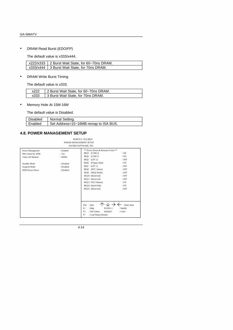
Figure 4.5: Power Management Setup• Power Management
The default value is Enabled.
Enabled Enable Green function.Disabled Disable Green function.
Please disable Green Function for Non-S CPU in OS/2, Unix, WindowNT & Novell system.
• PM Control by APM
The default value is No.
Yes Enable software APM function.No Disable software APM function.
• Video off Method
The default value is DPMS Support.
V/H SYNC + Blank BIOS will turn off V/H-SYNC when gets intoGreen mode for Green monitor power saving.
Blank Screen BIOS will only black monitor when gets intoGreen mode.
DPMS Support BIOS will use DPMS Standard to control VGAcard. (The Green type VGA card will turn ofV/H-SYNC automatically.)
• Standby Mode ( for Network Card using )
The default value is Disable.
Disable Disable Standby Mode.1 min - 1Hour
Setup the timer to enter Standby Mode.
• Suspend mode ( for CPU stop clock Mode )
The default value is Disable.
Disable Disable Suspend Mode.
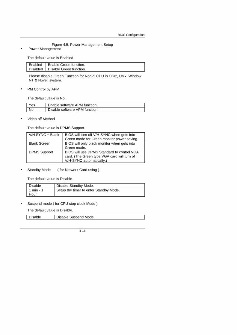
GA-586ATV
4-16
1 min - 1Hour
Setup the timer to enter Suspend Mode.
• HDD Power Down
The default value is Disable.
Disable Disable HDD Power Down mode function.1-15 mins Enable HDD enter Power Down mode between 1 to 15
mins.
4.9. PNP/PCI CONFIGURATION
ROM PCI / ISA BIOS
PNP/PCI CONFGURATION
AWARD SOFTWARE, INC.
: Select ItemESC
F1
F5
F7 : Load Setup Defaults
: Quit
: Help
: Old Values
PU/PD/+/-
(Shift)F2
: Modify
: Color
IRQ-3 assigned to
Resources Controlled by : Manual
: Legacy ISAIRQ-4 assigned to
IRQ-5 assigned to
IRQ-7 assigned to
IRQ-9 assigned to
IRQ-10 assigned to
IRQ-11 assigned to
IRQ-12 assigned to
IRQ-14 assigned to
IRQ-15 assigned to
DMA-0 assigned to
DMA-1 assigned to
DMA-6 assigned to
DMA-3 assigned to
DMA-5 assigned to
DMA-7 assigned to
: Legacy ISA
: Legacy ISA
: Legacy ISA
: Legacy ISA
Reset Configuration Data : Disabled
: PCI/ ISA PnP
: PCI/ ISA PnP
: PCI/ ISA PnP
: PCI/ ISA PnP
: PCI/ ISA PnP
: PCI/ ISA PnP
: PCI/ ISA PnP
: PCI/ ISA PnP
: PCI/ ISA PnP
: PCI/ ISA PnP
: Legacy ISA
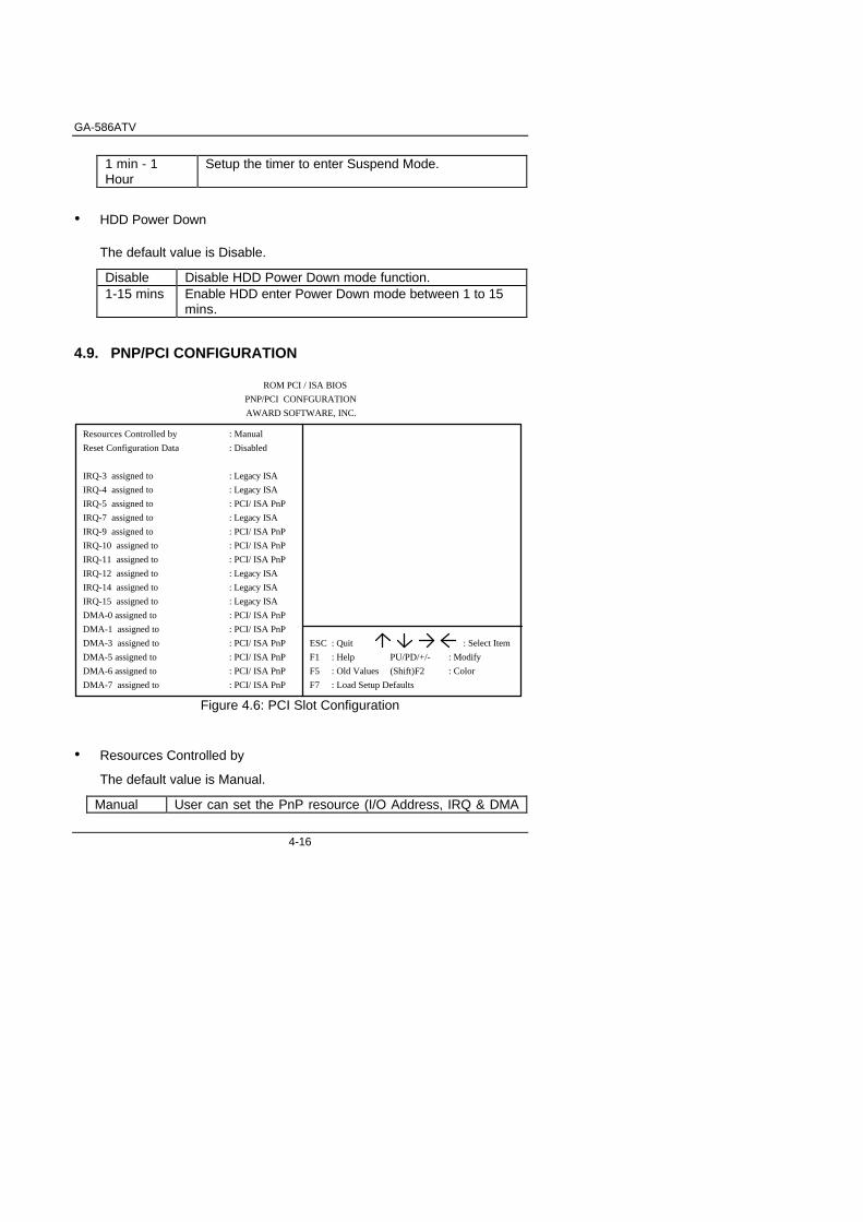
Figure 4.6: PCI Slot Configuration
• Resources Controlled by
The default value is Manual.
Manual User can set the PnP resource (I/O Address, IRQ & DMA
BIOS Configuration
4-17
channels) used by legacy ISA DEVICE.Auto BIOS automatically use these PnP resources.
• IRQ (3,4,5,7,9,10,11,12,14,15),DMA(0,1,3,5,6,7) assigned to
The default value is "Legacy ISA" or "PCI/ISA PnP".
Legacy ISA The resource is used by Legacy ISA device.PCI/ISA PnP The resource is used by PCI/ISA PnP device (PCI or
ISA).
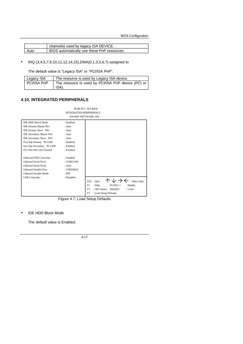
4.10. INTEGRATED PERIPHERALS
ROM PCI / ISA BIOS
INTEGRATED PERIPHERALS
AWARD SOFTWARE, INC.
: Select ItemESC
F1
F5
F7 : Load Setup Defaults
: Quit
: Help
: Old Values
PU/PD/+/-
(Shift)F2
: Modify
: Color
IDE Primary Master PIO
IDE HDD Block Mode : Enabled
: Auto
On-Chip Primary PCI IDE
PCI Slot IDE 2nd Channel
Onboard FDD Controller
: Auto
: Enabled
: COM1/3F8
: 378H/IRQ7
: SPP
IDE Primary Slave PIO
IDE Secondary Master PIO
IDE Secondary Slave PIO
On-Chip Secondary PCI IDE
Onboard Serial Port1
Onboard Serial Port2
Onboard Parallel Port
Onboard Parallel Mode
: Enabled
: Enabled
: Enabled
: Auto
: Auto
: Auto
USB Controller : Disabled
Figure 4.7: Load Setup Defaults
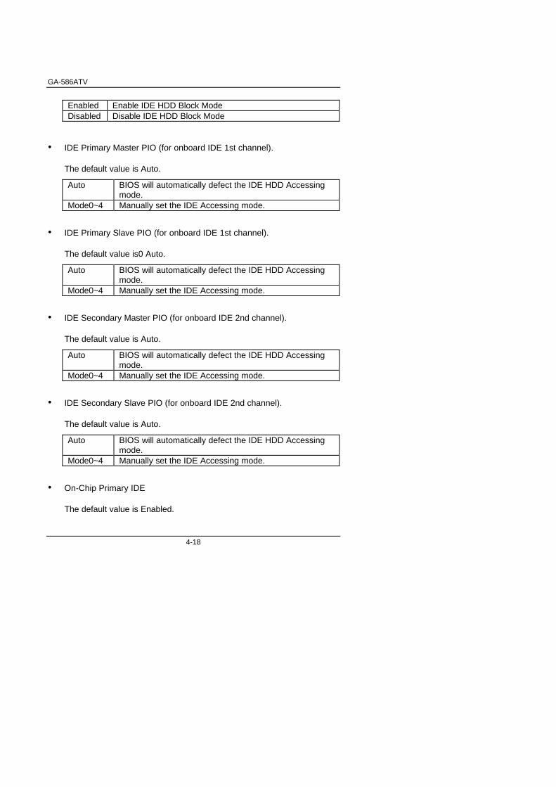
• IDE HDD Block Mode
The default value is Enabled.
GA-586ATV
4-18
Enabled Enable IDE HDD Block ModeDisabled Disable IDE HDD Block Mode
• IDE Primary Master PIO (for onboard IDE 1st channel).
The default value is Auto.
Auto BIOS will automatically defect the IDE HDD Accessingmode.
Mode0~4 Manually set the IDE Accessing mode.
• IDE Primary Slave PIO (for onboard IDE 1st channel).
The default value is0 Auto.
Auto BIOS will automatically defect the IDE HDD Accessingmode.
Mode0~4 Manually set the IDE Accessing mode.
• IDE Secondary Master PIO (for onboard IDE 2nd channel).
The default value is Auto.
Auto BIOS will automatically defect the IDE HDD Accessingmode.
Mode0~4 Manually set the IDE Accessing mode.
• IDE Secondary Slave PIO (for onboard IDE 2nd channel).
The default value is Auto.
Auto BIOS will automatically defect the IDE HDD Accessingmode.
Mode0~4 Manually set the IDE Accessing mode.
• On-Chip Primary IDE
The default value is Enabled.
BIOS Configuration
4-19
Enabled Enable onboard 1st channel IDE port.Disabled Disable onboard 1st channel IDE port.
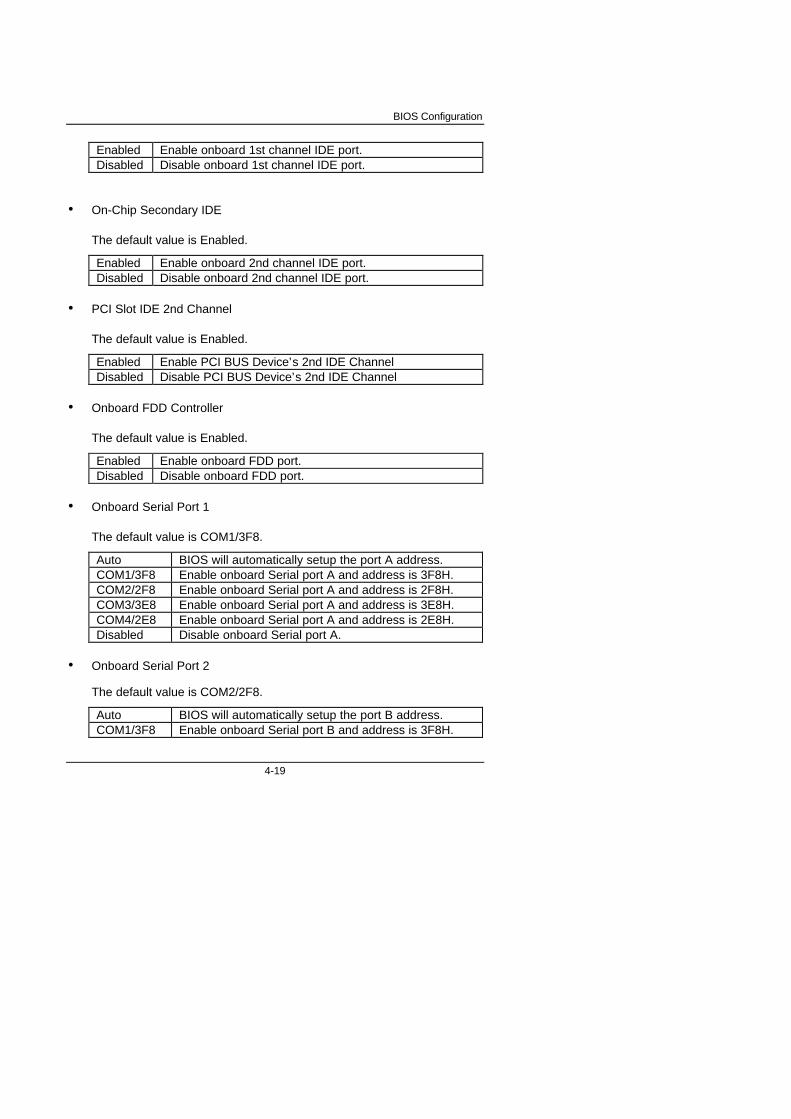
• On-Chip Secondary IDE
The default value is Enabled.
Enabled Enable onboard 2nd channel IDE port.Disabled Disable onboard 2nd channel IDE port.
• PCI Slot IDE 2nd Channel
The default value is Enabled.
Enabled Enable PCI BUS Device’s 2nd IDE ChannelDisabled Disable PCI BUS Device’s 2nd IDE Channel
• Onboard FDD Controller
The default value is Enabled.
Enabled Enable onboard FDD port.Disabled Disable onboard FDD port.
• Onboard Serial Port 1
The default value is COM1/3F8.
Auto BIOS will automatically setup the port A address.COM1/3F8 Enable onboard Serial port A and address is 3F8H.COM2/2F8 Enable onboard Serial port A and address is 2F8H.COM3/3E8 Enable onboard Serial port A and address is 3E8H.COM4/2E8 Enable onboard Serial port A and address is 2E8H.Disabled Disable onboard Serial port A.
• Onboard Serial Port 2
The default value is COM2/2F8.
Auto BIOS will automatically setup the port B address.COM1/3F8 Enable onboard Serial port B and address is 3F8H.
GA-586ATV
4-20
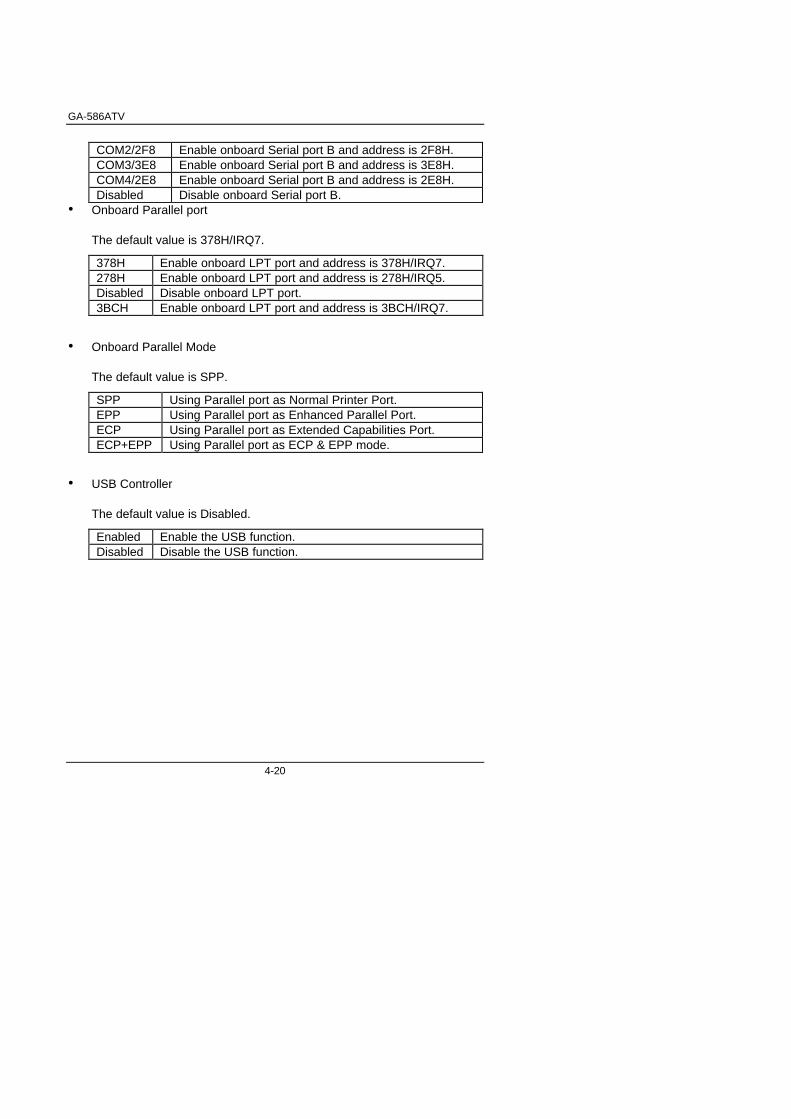
COM2/2F8 Enable onboard Serial port B and address is 2F8H.COM3/3E8 Enable onboard Serial port B and address is 3E8H.COM4/2E8 Enable onboard Serial port B and address is 2E8H.Disabled Disable onboard Serial port B.
• Onboard Parallel port
The default value is 378H/IRQ7.
378H Enable onboard LPT port and address is 378H/IRQ7.278H Enable onboard LPT port and address is 278H/IRQ5.Disabled Disable onboard LPT port.3BCH Enable onboard LPT port and address is 3BCH/IRQ7.
• Onboard Parallel Mode
The default value is SPP.
SPP Using Parallel port as Normal Printer Port.EPP Using Parallel port as Enhanced Parallel Port.ECP Using Parallel port as Extended Capabilities Port.ECP+EPP Using Parallel port as ECP & EPP mode.
• USB Controller
The default value is Disabled.
Enabled Enable the USB function.Disabled Disable the USB function.
BIOS Configuration
4-21
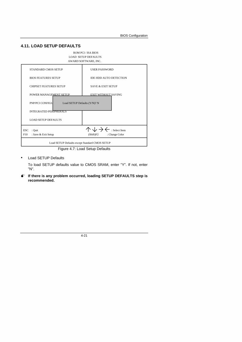
4.11. LOAD SETUP DEFAULTS
POWER MANAGEMENT SETUP
INTEGRATED PERIPHERALS
ROM PCI / ISA BIOS
LOAD SETUP DEFAULTS
AWARD SOFTWARE, INC.
STANDARD CMOS SETUP
BIOS FEATURES SETUP
CHIPSET FEATURES SETUP
PNP/PCI CONFIGURATION
LOAD SETUP DEFAULTS
USER PASSWORD
SAVE & EXIT SETUP
EXIT WITHOUT SAVING
ESC
F10
: Quit
: Save & Exit Setup (Shift)F2
: Select Item
: Change Color
Load SETUP Defaults (Y/N)? N
Load SETUP Defaults except Standard CMOS SETUP
IDE HDD AUTO DETECTION
Figure 4.7: Load Setup Defaults
• Load SETUP Defaults
To load SETUP defaults value to CMOS SRAM, enter "Y". If not, enter"N".
M If there is any problem occurred, loading SETUP DEFAULTS step isrecommended.
GA-586ATV
4-22
4.12. USER PASSWORD
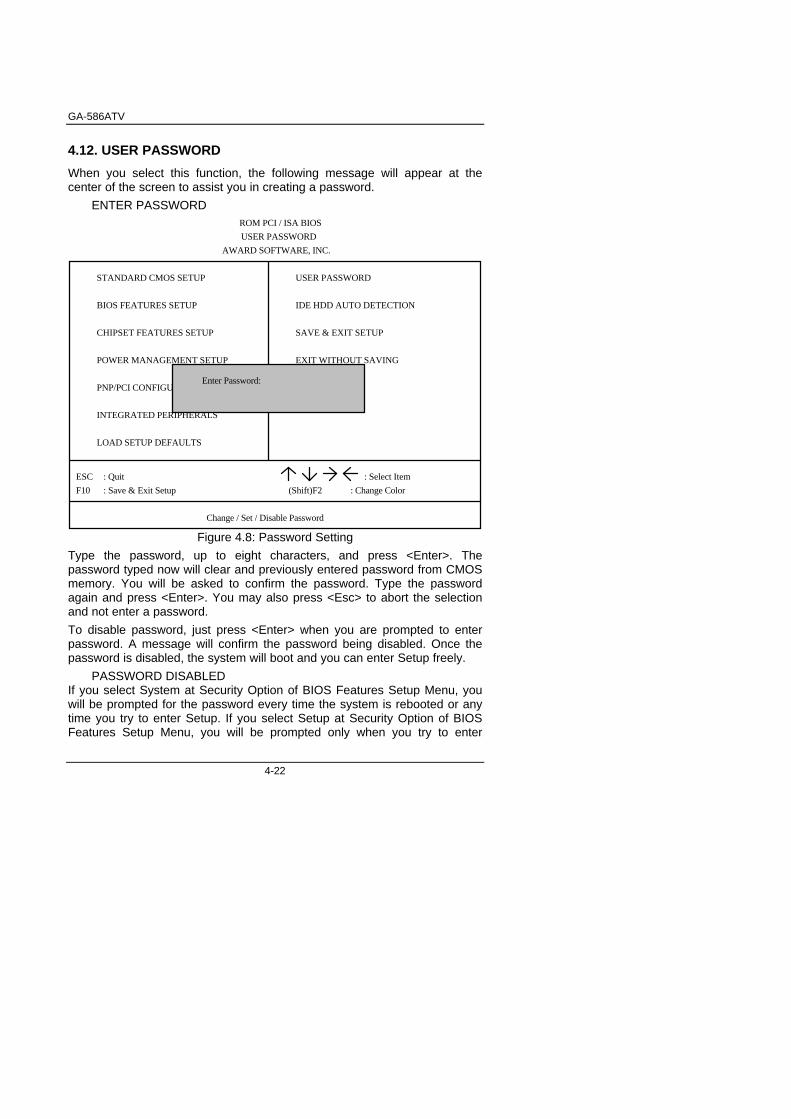
When you select this function, the following message will appear at thecenter of the screen to assist you in creating a password.
ENTER PASSWORD
POWER MANAGEMENT SETUP
INTEGRATED PERIPHERALS
ROM PCI / ISA BIOS
USER PASSWORD
AWARD SOFTWARE, INC.
STANDARD CMOS SETUP
BIOS FEATURES SETUP
CHIPSET FEATURES SETUP
PNP/PCI CONFIGURATION
LOAD SETUP DEFAULTS
USER PASSWORD
SAVE & EXIT SETUP
EXIT WITHOUT SAVING
ESC
F10
: Quit
: Save & Exit Setup (Shift)F2
: Select Item
: Change Color
Enter Password:
Change / Set / Disable Password
IDE HDD AUTO DETECTION
Figure 4.8: Password Setting
Type the password, up to eight characters, and press <Enter>. Thepassword typed now will clear and previously entered password from CMOSmemory. You will be asked to confirm the password. Type the passwordagain and press <Enter>. You may also press <Esc> to abort the selectionand not enter a password.
To disable password, just press <Enter> when you are prompted to enterpassword. A message will confirm the password being disabled. Once thepassword is disabled, the system will boot and you can enter Setup freely.
PASSWORD DISABLEDIf you select System at Security Option of BIOS Features Setup Menu, youwill be prompted for the password every time the system is rebooted or anytime you try to enter Setup. If you select Setup at Security Option of BIOSFeatures Setup Menu, you will be prompted only when you try to enter
BIOS Configuration
4-23
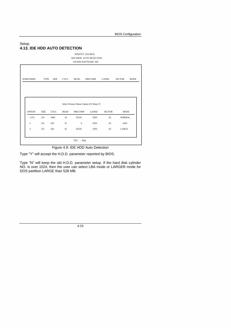
Setup.4.13. IDE HDD AUTO DETECTION
ROM PCI / ISA BIOS
IDE HDDD AUTO DETECTION
AWARD SOFTWARE, INC.
ESC
CYLS. HEAD PRECOMP LANDZ SECTOR
Select Primary Master Option (N=Skip): N
: Skip
SIZETYPEHARD DISKS MODE
OPTION SIZE CYLS. HEAD PRECOMP LANDZ SECTOR MODE
1 (Y)
2
3
521
521
521
1060
530
530
16
32
32
65535
65535
0
1059
1059
1059
63
63
63
NORMAL
LBA
LARGE
Figure 4.9: IDE HDD Auto Detection
Type "Y" will accept the H.D.D. parameter reported by BIOS.
Type "N" will keep the old H.D.D. parameter setup. If the hard disk cylinderNO. is over 1024, then the user can select LBA mode or LARGER mode forDOS partition LARGE than 528 MB.
GA-586ATV
4-24
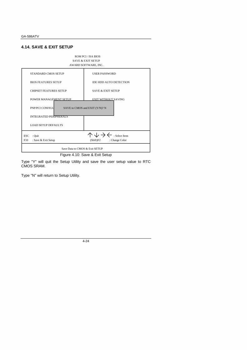
4.14. SAVE & EXIT SETUP
POWER MANAGEMENT SETUP
INTEGRATED PERIPHERALS
PNP/PCI CONFIGURATION
ROM PCI / ISA BIOS
SAVE & EXIT SETUP
AWARD SOFTWARE, INC.
STANDARD CMOS SETUP
BIOS FEATURES SETUP
CHIPSET FEATURES SETUP
LOAD SETUP DEFAULTS
USER PASSWORD
SAVE & EXIT SETUP
EXIT WITHOUT SAVING
ESC
F10
: Quit
: Save & Exit Setup (Shift)F2
: Select Item
: Change Color
SAVE to CMOS and EXIT (Y/N)? N
Save Data to CMOS & Exit SETUP
IDE HDD AUTO DETECTION
Figure 4.10: Save & Exit Setup
Type "Y" will quit the Setup Utility and save the user setup value to RTCCMOS SRAM.
Type "N" will return to Setup Utility.
BIOS Configuration
4-25
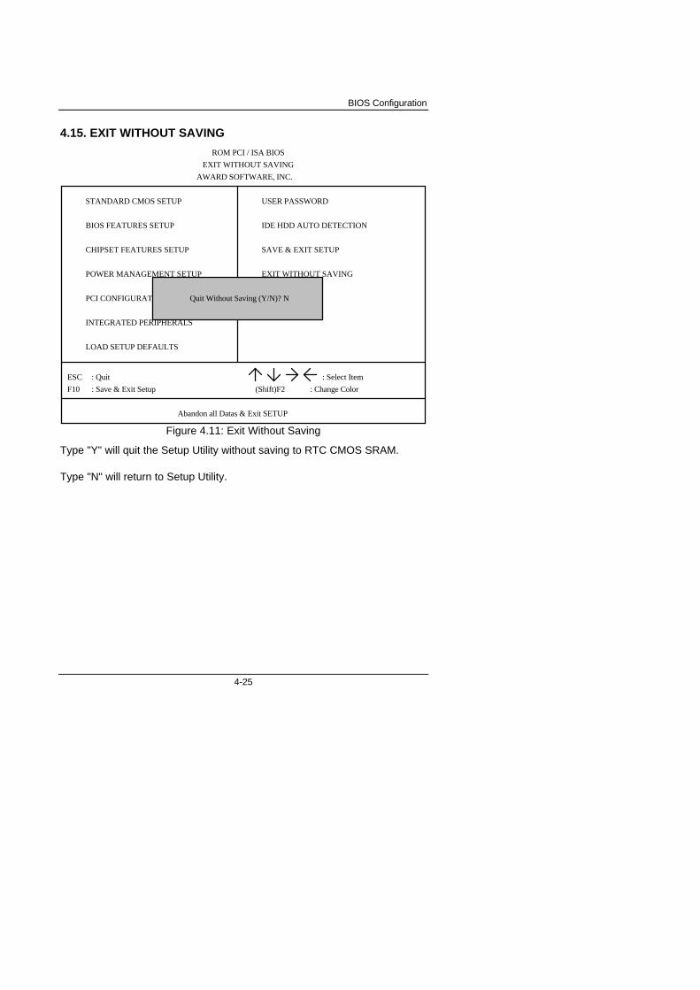
4.15. EXIT WITHOUT SAVING
POWER MANAGEMENT SETUP
ROM PCI / ISA BIOS
EXIT WITHOUT SAVING
AWARD SOFTWARE, INC.
STANDARD CMOS SETUP
BIOS FEATURES SETUP
CHIPSET FEATURES SETUP
PCI CONFIGURATION
INTEGRATED PERIPHERALS
USER PASSWORD
SAVE & EXIT SETUP
EXIT WITHOUT SAVING
ESC
F10
: Quit
: Save & Exit Setup (Shift)F2
: Select Item
: Change Color
Quit Without Saving (Y/N)? N
Abandon all Datas & Exit SETUP
IDE HDD AUTO DETECTION
LOAD SETUP DEFAULTS
Figure 4.11: Exit Without Saving
Type "Y" will quit the Setup Utility without saving to RTC CMOS SRAM.
Type "N" will return to Setup Utility.

GA-586ATV
5-1
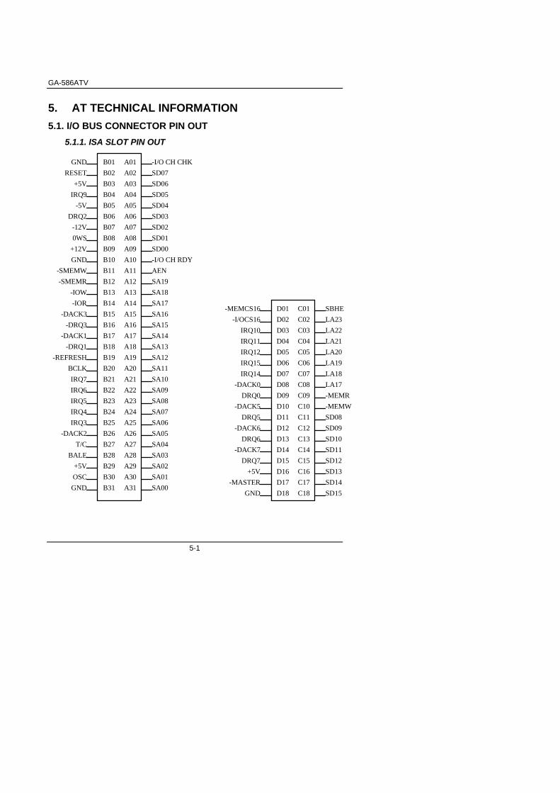
5. AT TECHNICAL INFORMATION
5.1. I/O BUS CONNECTOR PIN OUT
5.1.1. ISA SLOT PIN OUT
B23
B24
B31
B05
B07
B10
B13
B15
B19
B21
B25
B29
B02
B04
B08
B11
B14
B17
B20
B26
B27
B01
B03
B06
B09
B12
B16
B18
B22
B28
B30
-REFRESH
A05
A07
A10
A13
A15
A19
A21
A02
A04
A08
A11
A14
A17
A20
A01
A03
A06
A09
A12
A16
A18
A22
A23
A24
A31
A25
A29
A26
A27
A28
A30
D05
D07
D10
D13
D15
D02
D04
D08
D11
D14
D17
D01
D03
D06
D09
D12
D16
D18
C05
C07
C10
C13
C15
C02
C04
C08
C11
C14
C17
C01
C03
C06
C09
C12
C16
C18
SA19
SA18
SA17
SA16
SA15
SA14
SA13
SA12
SA11
SA10
SA09
SA08
SA07
SA06
SA05
SA04
SA03
SA02
SA01
SA00
SD07
SD06
SD04
SD03
SD02
SD05
SD00
SD01
-I/O CH RDY
AEN
-I/O CH CHKGND
RESET
+5V
IRQ9
-5V
DRQ2
-12V
0WS
+12V
GND
-SMEMW
-SMEMR
-IOW
-IOR
-DACK3
-DRQ3
-DACK1
-DRQ1
BCLK
IRQ7
IRQ6
IRQ5
IRQ4
IRQ3
-DACK2
T/C
BALE
+5V
OSC
GND
-MEMCS16
-I/OCS16
IRQ10
IRQ11
IRQ12
IRQ15
IRQ14
-DACK0
DRQ0
-DACK5
DRQ5
-DACK6
DRQ6
-DACK7
DRQ7
+5V
-MASTER
GND
SBHE
LA23
LA22
LA21
LA20
LA19
LA18
LA17
-MEMR
-MEMW
SD08
SD09
SD10
SD11
SD12
SD13
SD14
SD15
AT Technical Information
5-2
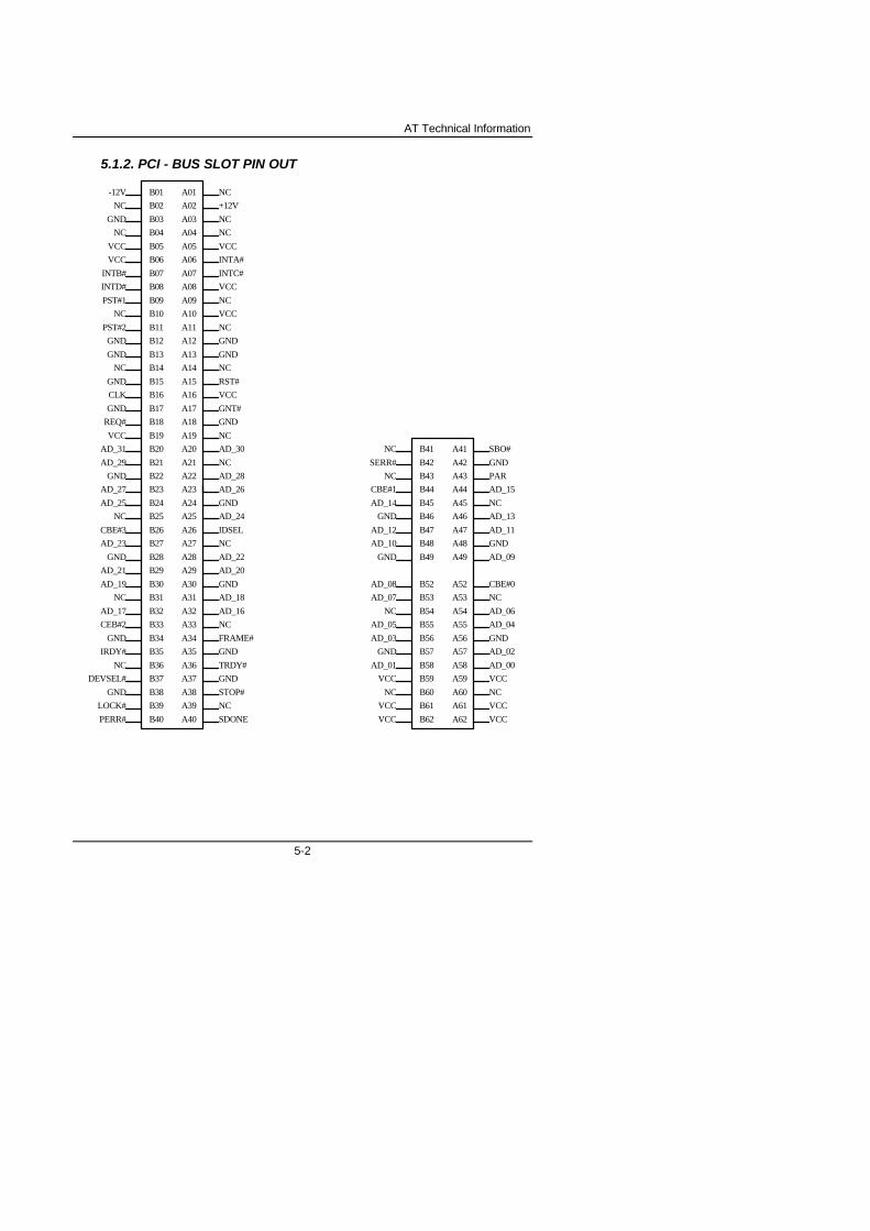
5.1.2. PCI - BUS SLOT PIN OUT
B23
B24
B31
B05
B07
B10
B13
B15
B19
B21
B25
B29
B02
B04
B08
B11
B14
B17
B20
B26
B27
B01
B03
B06
B09
B12
B16
B18
B22
B28
B30
A05
A07
A10
A13
A15
A19
A21
A02
A04
A08
A11
A14
A17
A20
A01
A03
A06
A09
A12
A16
A18
A22
A23
A24
A31
A25
A29
A26
A27
A28
A30
B33
B34
B41
B35
B39
B36
B37
B32
B38
B40
A32
A33
A34
A41
A35
A39
A36
A37
A38
A40
B43
B44
B45
B49
B46
B47
B42
B48
A42
A43
A44
A45
A49
A46
A47
A48
B53
B54
B61
B55
B59
B56
B57
B52
B58
B60
A52
A53
A54
A61
A55
A59
A56
A57
A58
A60
B62 A62
NC
+12V
NC
NC
VCC
INTA#
INTC#
VCC
NC
VCC
NC
GND
GND
NC
NC
NC
NC
NC
NC
RST#
VCC
GNT#
GND
AD_30
AD_28
AD_26
GND
AD_24
IDSEL
NC
AD_22
AD_20
GND
AD_18
AD_16
FRAME#
GND
TRDY#
GND
STOP#
SDONE
SBO#
GND
PAR
AD_15
AD_13
AD_11
GND
AD_09
CBE#0
NC
AD_06
AD_04
GND
AD_02
AD_00
VCC
NC
VCC
VCC
NC
SERR#
NC
CBE#1
AD_14
GND
AD_12
AD_10
GND
AD_08
AD_07
NC
AD_05
AD_03
GND
AD_01
VCC
NC
VCC
VCC
AD_25
NC
CBE#3
AD_23
GND
AD_21
AD_19
NC
AD_17
CEB#2
GND
IRDY#
NC
DEVSEL#
GND
LOCK#
PERR#
VCC
INTB#
INTD#
PST#1
NC
PST#2
GND
GND
NC
GND
CLK
GND
REQ#
VCC
AD_31
AD_29
GND
AD_27
-12V
NC
GND
NC
VCC
GA-586ATV
5-3
5.2. I/O & MEMORY MAPMEMORY MAP: [0000000-009FFFF] System memory used by DOS and application program.
[00A0000-00BFFFF] Display buffer memory for VGA/ EGA/CGA/MONOCHROME adapter.[00C0000-00DFFFF] Reserved for I/O device BIOS ROM or RAM buffer.[00E0000-00EFFFF] Reserved for PCI device ROM.[00F0000-00FFFFF] System BIOS ROM.[0100000-BFFFFFF] System extension memory.
I/O MAP: [000-01F] DMA controller.(Master)[020-021] INTERRUPT controller.(Master)[022-023] CHIPSET control registers I/O ports.[040-05F] TIMER control registers.[060-06F] KEYBOARD interface controller.(8042)[070-07F] RTC ports & CMOS I/O ports.[080-09F] DMA register.[0A0-0BF] INTERRUPT controller.(Slave)[0C0-0DF] DMA controller.(Slave)[0F0-0FF] MATH COPROCESSOR[1F0-1F8] HARD DISK controller.[278-27F] PARALLEL port-2.[2B0-2DF] GRAPHICS adapter controller.[2F8-2FF] SERIAL port-2.[360-36F] NETWORK ports.[378-37F] PARALLEL port-1[3B0-3BF] MONOCHROME & PRINTER adapter.[3C0-3CF] EGA adapter.[3D0-3DF] CGA adapter.[3F0-3F7] FLOPPY DISK controller.[3F8-3FF] SERIAL port-1.
5.3. TIMER & DMA CHANNELS MAP
TIMER MAP: TIMER Channel-0 System timer interruptTIMER Channel-1 DRAM REFRESH requestTIMER Channel-2 SPEAKER tone generator
DMA CHANNELS: DMA Channel-0 AvailableDMA Channel-1 IBM SDLCDMA Channel-2 FLOPPY DISK adapterDMA Channel-3 AvailableDMA Channel-4 Cascade for DMA controller 1DMA Channel-5 AvailableDMA Channel-6 AvailableDMA Channel-7 Available
AT Technical Information
5-4
5.4. INTERRUPT MAP
NMI: Parity check error
IRQ (H/W): 0 System TIMER interrupt from TIMER-01 KEYBOARD output buffer full2 Cascade for IRQ 8-153 SERIAL port 24 SERIAL port 15 PARALLEL port 26 FLOPPY DISK adapter7 PARALLEL port 18 RTC clock9 Available10 Available11 Available12 Available13 MATH coprocessor14 HARD DISK adapter15 Available
GA-586ATV
5-5
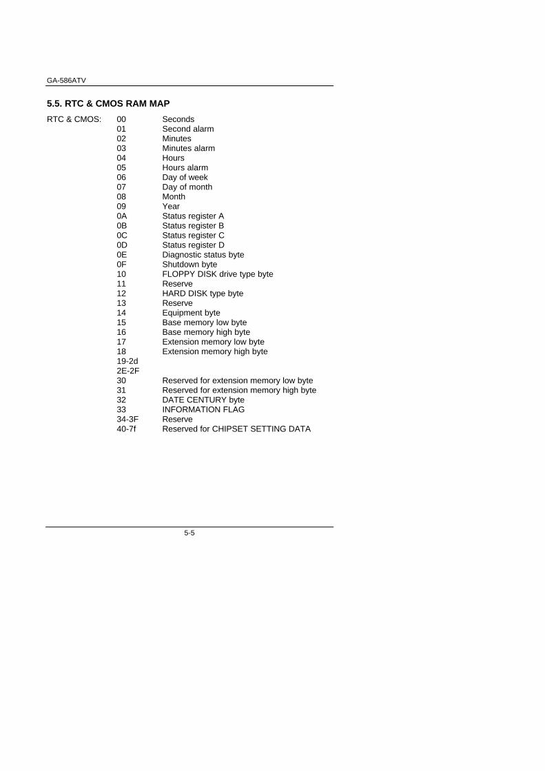
5.5. RTC & CMOS RAM MAP
RTC & CMOS: 00 Seconds01 Second alarm02 Minutes03 Minutes alarm04 Hours05 Hours alarm06 Day of week07 Day of month08 Month09 Year0A Status register A0B Status register B0C Status register C0D Status register D0E Diagnostic status byte0F Shutdown byte10 FLOPPY DISK drive type byte11 Reserve12 HARD DISK type byte13 Reserve14 Equipment byte15 Base memory low byte16 Base memory high byte17 Extension memory low byte18 Extension memory high byte19-2d2E-2F30 Reserved for extension memory low byte31 Reserved for extension memory high byte32 DATE CENTURY byte33 INFORMATION FLAG34-3F Reserve40-7f Reserved for CHIPSET SETTING DATA

Appendix A: Post Message
A-1
APPENDIX A: POST MESSAGE
When the BIOS encounters an error that requires the user to correctsomething, either a beep code will sound or a message will be displayed in abox in the middle of the screen and the message PRESS F1 TO CONTINUE,CTRL-ALT-ESC OR DEL TO ENTER SETUP will be shown in theinformation box at the bottom.
• POST BEEP
Currently there is only one beep code in BIOS. This code indicates thata video error has occurred and the BIOS cannot initialize the videoscreen to display any additional information. This beep code consists ofa single long beep followed by two short beeps.
• ERROR MESSAGE
Once or more of the following messages may be displayed if the BIOSdetects an error during the POST. This list includes message for boththe ISA and the EISA BIOS.
⌦ CMOS BATTERY HAS FAILED
CMOS battery is no longer functional. It should be replaced.
⌦ CMOS CHECKSUM ERROR
Checksum of CMOS is incorrect. This can indicate that CMOS hasbecome corrupt. This error may have been caused by a weak battery.Check the battery and replace if necessary.
⌦ DISK BOOT FAILURE, INSERT SYSTEM DISK AND PRESS ENTER
No boot device was found. Insert a system disk into Drive A: and press<Enter>. If you assumed the system would boot from the hard drive,make sure the controller is inserted correctly and all cables are properlyattached. Also be sure the disk is formatted as a boot device. Thenreboot the system.
⌦ DISKETTE DRIVES OR TYPES MISMATCH ERROR - RUN SETUP
Type of diskette drive installed in the system is different from the CMOSdefinition. Run Setup to re-configure the drive type correctly.
GA-586ATV
A-2
⌦ DISPLAY SWITCH IS SET INCORRECTLY
Display switch on the motherboard can be set to either monochrome orcolor. This indicates the switch is set to a different setting than indicatedin Setup. Determine which setting is correct, and then either turn off thesystem and change the jumper, or enter Setup and change the VIDEOselection.
⌦ DISPLAY TYPE HAS CHANGED SINCE LAST BOOT
Since last powering off the system, the display adapter has beenchanged. You must configure the system for the new display type.
⌦ EISA Configuration Checksum Error
PLEASE RUN EISA CONFIGURATION UTILITY
The EISA non-volatile RAM checksum is incorrect or cannot correctlyread the EISA slot. This can indicate either the EISA non-volatilememory has become corrupt or the slot has configured incorrectly. Alsobe sure the card is installed firmly in the slot.
⌦ EISA Configuration Is Not Complete
PLEASE RUN EISA CONFIGURATION UTILITY
The slot configuration information stored in the EISA non-volatilememory is incomplete.
F When either of these errors appear, the system will boot in ISA mode,which allows you to run the EISA Configuration Utility.
⌦ ERROR ENCOUNTERED INITIALIZING HARD DRIVE
Hard drive cannot be initialized. Be sure the adapter is installed correctlyand all cables are correctly and firmly attached. Also be sure the correcthard drive type is selected in Setup.
⌦ ERROR INITIALIZING HARD DISK CONTROLLER
Cannot initialize controller. Make sure the cord is correctly and firmlyinstalled in the bus. Be sure the correct hard drive type is selected inSetup. Also check to see if any jumper needs to be set correctly in thehard drive.
Appendix A: Post Message
A-3
⌦ FLOPPY DISK CNTRLR ERROR OR NO CNTRLR PRESENT
Cannot find or initialize the floppy drive controller. Make sure thecontroller is installed correctly and firmly. If there are no floppy drivesinstalled, be sure the Diskette Drive selection in Setup is set to NONE.
⌦ Invalid EISA Configuration
PLEASE RUN EISA CONFIGURATION UTILITY
The non-volatile memory containing EISA configuration information wasprogrammed incorrectly or has become corrupt. Re-run EISAconfiguration utility to correctly program the memory.
F When this error appears, the system will boot in ISA mode, which allowsyou to run the EISA Configuration Utility.
⌦ KEYBOARD ERROR OR NO KEYBOARD PRESENT
Cannot initialize the keyboard. Make sure the keyboard is attachedcorrectly and no keys are being pressed during the boot.
If you are purposely configuring the system without a keyboard, set theerror halt condition in Setup to HALT ON ALL, BUT KEYBOARD. Thiswill cause the BIOS to ignore the missing keyboard and continue theboot.
⌦ Memory Address Error at ...
Indicates a memory address error at a specific location. You can usethis location along with the memory map for your system to find andreplace the bad memory chips.
⌦ Memory parity Error at ...
Indicates a memory parity error at a specific location. You can use thislocation along with the memory map for your system to find and replacethe bad memory chips.
⌦ MEMORY SIZE HAS CHANGED SINCE LAST BOOT
Memory has been added or removed since the last boot. In EISA modeuse Configuration Utility to re-configure the memory configuration. InISA mode enter Setup and enter the new memory size in the memoryfields.
GA-586ATV
A-4
⌦ Memory Verify Error at ...
Indicates an error verifying a value already written to memory. Use thelocation along with your system's memory map to locate the bad chip.
⌦ OFFENDING ADDRESS NOT FOUND
This message is used in conjunction with the I/O CHANNEL CHECK andRAM PARITY ERROR messages when the segment that has caused theproblem cannot be isolated.
⌦ OFFENDING SEGMENT:
This message is used in conjunction with the I/O CHANNEL CHECK andRAM PARITY ERROR messages when the segment that has caused theproblem has been isolated.
⌦ PRESS A KEY TO REBOOTThis will be displayed at the bottom screen when an error occurs thatrequires you to reboot. Press any key and the system will reboot.
⌦ PRESS F1 TO DISABLE NMI, F2 TO REBOOTWhen BIOS detects a Non-maskable Interrupt condition during boot, thiswill allow you to disable the NMI and continue to boot, or you can rebootthe system will the NMI enabled.
⌦ RAM PARITY ERROR - CHECKING FOR SEGMENT ...Indicates a parity error in Random Access Memory.
⌦ Should Be Empty But EISA Board Found
PLEASE RUN EISA CONFIGURATION UTILITYA valid board ID was found in a slot that was configured as having noboard ID.
F When this error appears, the system will boot in ISA mode, which allowsyou to run the EISA Configuration Utility.
⌦ Should Have EISA Board But Not Found
PLEASE RUN EISA CONFIGURATION UTILITY
The board installed is not responding to the ID request, or no board IDhas been found in the indicated slot.
Appendix A: Post Message
A-5
F When this error appears, the system will boot in ISA mode, which allowsyou to run the EISA Configuration Utility.
⌦ Slot Not Empty
Indicates that a slot designated as empty by the EISA ConfigurationUtility actually contains a board.
F When this error appears, the system will boot in ISA mode, which allowsyou to run the EISA Configuration Utility.
⌦ SYSTEM HALTED, (CTRL-ALT-DEL) TO REBOOT ...
Indicates the present boot attempt has been aborted and the systemmust be rebooted. Press and hold down the CTRL and ALT keys andpress DEL.
⌦ Wrong Board In Slot
PLEASE RUN EISA CONFIGURATION UTILITY
The board ID does not match the ID stored in the EISA non-volatilememory.
F When this error appears, the system will boot in ISA mode, which allowsyou to run the EISA Configuration Utility.

GA-586ATV
B-1
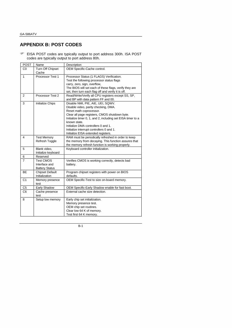
APPENDIX B: POST CODES
F EISA POST codes are typically output to port address 300h. ISA POSTcodes are typically output to port address 80h.
POST Name DescriptionC0 Turn Off Chipset
CacheOEM Specific-Cache control.
1 Processor Test 1 Processor Status (1 FLAGS) Verification.Test the following processor status flagscarry, zero, sign, overflow,The BIOS will set each of these flags, verify they areset, then turn each flag off and verify it is off.
2 Processor Test 2 Read/Write/Verify all CPU registers except SS, SP,and BP with data pattern FF and 00.
3 Initialize Chips Disable NMI, PIE, AIE, UEI, SQWV.Disable video, parity checking, DMA.Reset math coprocessor.Clear all page registers, CMOS shutdown byte.Initialize timer 0, 1, and 2, including set EISA timer to aknown state.Initialize DMA controllers 0 and 1.Initialize interrupt controllers 0 and 1.Initialize EISA extended registers.
4 Test MemoryRefresh Toggle
RAM must be periodically refreshed in order to keepthe memory from decaying. This function assures thatthe memory refresh function is working properly.
5 Blank video,Initialize keyboard
Keyboard controller initialization.
6 Reserved7 Test CMOS
Interface andBattery Status
Verifies CMOS is working correctly, detects badbattery.
BE Chipset DefaultInitialization
Program chipset registers with power on BIOSdefaults.
C1 Memory presencetest
OEM Specific-Test to size on-board memory.
C5 Early Shadow OEM Specific-Early Shadow enable for fast boot.C6 Cache presence
testExternal cache size detection.
8 Setup low memory Early chip set initialization.Memory presence test.OEM chip set routines.Clear low 64 K of memory.Test first 64 K memory.
Appendix B: Post Codes
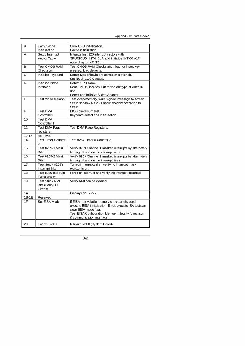
B-2
9 Early CacheInitialization
Cyrix CPU initialization.Cache initialization.
A Setup InterruptVector Table
Initialize first 120 interrupt vectors withSPURIOUS_INT-HDLR and initialize INT 00h-1Fhaccording to INT_TBL.
B Test CMOS RAMChecksum
Test CMOS RAM Checksum, if bad, or insert keypressed, load defaults.
C Initialize keyboard Detect type of keyboard controller (optional).Set NUM_LOCK status.
D Initialize VideoInterface
Detect CPU clock.Read CMOS location 14h to find out type of video inuse.Detect and Initialize Video Adapter.
E Test Video Memory Test video memory, write sign-on message to screen.Setup shadow RAM - Enable shadow according toSetup.
F Test DMAController 0
BIOS checksum test.Keyboard detect and initialization.
10 Test DMAController 1
11 Test DMA Pageregisters
Test DMA Page Registers.
12-13 Reserved14 Test Timer Counter
2Test 8254 Timer 0 Counter 2.
15 Test 8259-1 MaskBits
Verify 8259 Channel 1 masked interrupts by alternatelyturning off and on the interrupt lines.
16 Test 8259-2 MaskBits
Verify 8259 Channel 2 masked interrupts by alternatelyturning off and on the interrupt lines.
17 Test Stuck 8259'sInterrupt Bits
Turn off interrupts then verify no interrupt maskregister is on.
18 Test 8259 InterruptFunctionality
Force an interrupt and verify the interrupt occurred.
19 Test Stuck NMIBits (Parity/IOCheck)
Verify NMI can be cleared.
1A Display CPU clock.1B-1E Reserved1F Set EISA Mode If EISA non-volatile memory checksum is good,
execute EISA initialization. If not, execute ISA tests anclear EISA mode flag.Test EISA Configuration Memory Integrity (checksum& communication interface).
20 Enable Slot 0 Initialize slot 0 (System Board).
GA-586ATV
B-3
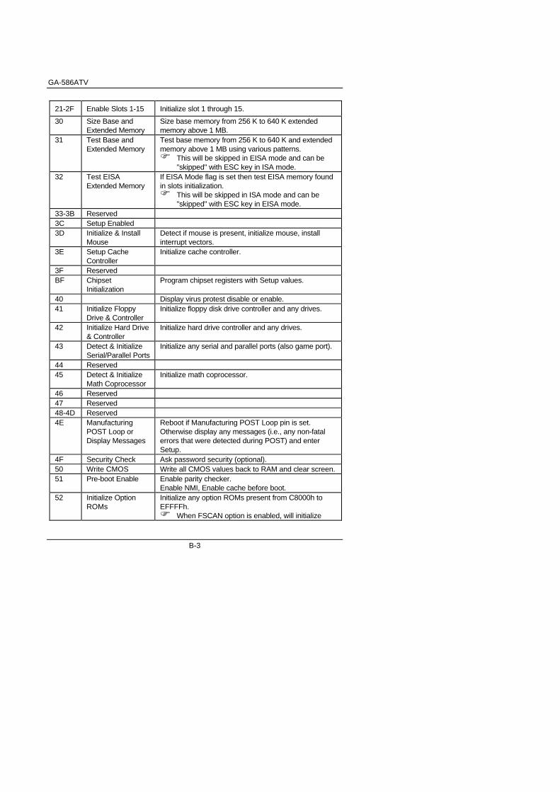
21-2F Enable Slots 1-15 Initialize slot 1 through 15.
30 Size Base andExtended Memory
Size base memory from 256 K to 640 K extendedmemory above 1 MB.
31 Test Base andExtended Memory
Test base memory from 256 K to 640 K and extendedmemory above 1 MB using various patterns.F This will be skipped in EISA mode and can be
"skipped" with ESC key in ISA mode.32 Test EISA
Extended MemoryIf EISA Mode flag is set then test EISA memory foundin slots initialization.F This will be skipped in ISA mode and can be
"skipped" with ESC key in EISA mode.33-3B Reserved3C Setup Enabled3D Initialize & Install
MouseDetect if mouse is present, initialize mouse, installinterrupt vectors.
3E Setup CacheController
Initialize cache controller.
3F ReservedBF Chipset
InitializationProgram chipset registers with Setup values.
40 Display virus protest disable or enable.41 Initialize Floppy
Drive & ControllerInitialize floppy disk drive controller and any drives.
42 Initialize Hard Drive& Controller
Initialize hard drive controller and any drives.
43 Detect & InitializeSerial/Parallel Ports
Initialize any serial and parallel ports (also game port).
44 Reserved45 Detect & Initialize
Math CoprocessorInitialize math coprocessor.
46 Reserved47 Reserved48-4D Reserved4E Manufacturing
POST Loop orDisplay Messages
Reboot if Manufacturing POST Loop pin is set.Otherwise display any messages (i.e., any non-fatalerrors that were detected during POST) and enterSetup.
4F Security Check Ask password security (optional).50 Write CMOS Write all CMOS values back to RAM and clear screen.51 Pre-boot Enable Enable parity checker.
Enable NMI, Enable cache before boot.52 Initialize Option
ROMsInitialize any option ROMs present from C8000h toEFFFFh.F When FSCAN option is enabled, will initialize

Appendix B: Post Codes
B-4
from C8000h to F7FFFh.53 Initialize Time
ValueInitialize time value in 40h: BIOS area.
60 Setup Virus Protect Setup virus protect according to Setup61 Set Boot Speed Set system speed for boot62 Setup NumLock Setup NumLock status according to Setup63 Boot Attempt Set low stack.
Boot via INT 19h.B0 Spurious If interrupt occurs in protected mode.B1 Unclaimed NMI If unmasked NMI occurs, display
Press F1 to disable NMI, F2 reboot.E1-EF Setup Pages E1 - Page 1, E2 - Page 2, etc.FF Boot
GA-586ATV
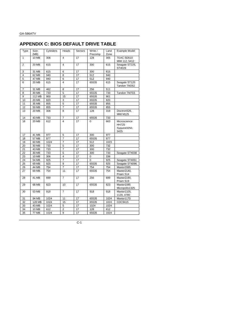
C-1
APPENDIX C: BIOS DEFAULT DRIVE TABLEType Size
(MB)Cylinders Heads Sectors Write /
PrecompLandZone
Example Model
1 10 MB 306 4 17 128 305 TEAC SD510MMI 112, 5412
2 20 MB 615 4 17 300 615 Seagate ST225,ST4026
3 31 MB 615 6 17 300 6154 62 MB 940 8 17 512 9405 47 MB 940 6 17 512 9406 20 MB 615 4 17 65535 615 Seagate ST125
Tandon TM2627 31 MB 462 8 17 256 5118 30 MB 733 5 17 65535 733 Tandon TM7039 112 MB 900 15 17 65535 90110 20 MB 820 3 17 65535 82011 35 MB 855 5 17 65535 85512 50 MB 855 7 17 65535 85513 20 MB 306 8 17 128 319 Disctron526,
MMI M12514 43 MB 733 7 17 65535 73316 20 MB 612 4 17 0 663 Microscience
HH725Syquest3250,3425
17 41 MB 977 5 17 300 97718 57 MB 977 7 17 65535 97719 60 MB 1024 7 17 512 102320 30 MB 733 5 17 300 73221 43 MB 733 7 17 300 73222 30 MB 733 5 17 300 733 Seagate ST403823 10 MB 306 4 17 0 33624 54 MB 925 7 17 0 925 Seagate ST405125 69 MB 925 9 17 65535 925 Seagate ST409626 44 MB 754 7 17 754 754 Maxtor208527 69 MB 754 11 17 65535 754 Maxtor2140,
Priam S1428 41 MB 699 7 17 256 699 Maxtor2190,
Priam S1929 68 MB 823 10 17 65535 823 Maxtor1085
Micropolis132530 53 MB 918 7 17 918 918 Maxtor1105,
1120, 478031 94 MB 1024 11 17 65535 1024 Maxtor117032 128 MB 1024 15 17 65535 1024 CDC941533 43 MB 1024 5 17 1024 102434 10 MB 612 2 17 128 61235 77 MB 1024 9 17 65535 1024
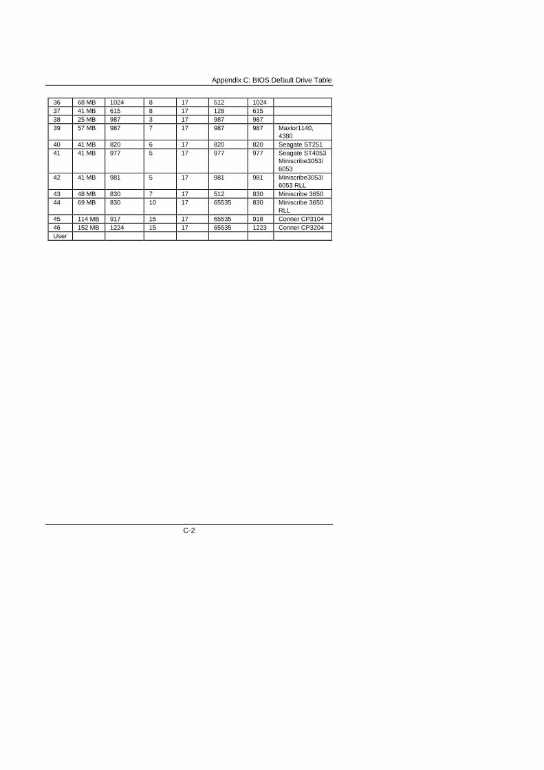
Appendix C: BIOS Default Drive Table
C-2
36 68 MB 1024 8 17 512 102437 41 MB 615 8 17 128 61538 25 MB 987 3 17 987 98739 57 MB 987 7 17 987 987 Maxtor1140,
438040 41 MB 820 6 17 820 820 Seagate ST25141 41 MB 977 5 17 977 977 Seagate ST4053
Miniscribe3053/6053
42 41 MB 981 5 17 981 981 Miniscribe3053/6053 RLL
43 48 MB 830 7 17 512 830 Miniscribe 365044 69 MB 830 10 17 65535 830 Miniscribe 3650
RLL45 114 MB 917 15 17 65535 918 Conner CP310446 152 MB 1224 15 17 65535 1223 Conner CP3204User
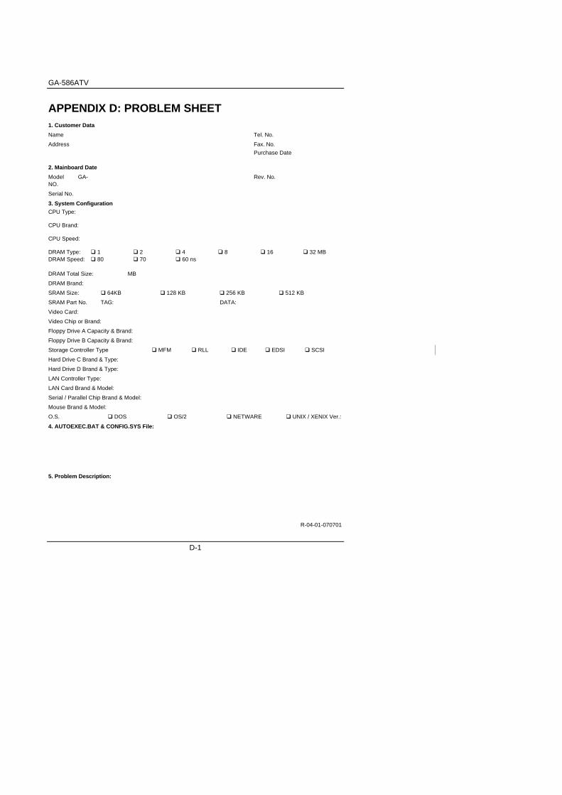
GA-586ATV
D-1
APPENDIX D: PROBLEM SHEET1. Customer Data
Name Tel. No.
Address Fax. No.
Purchase Date
2. Mainboard Date
ModelNO.
GA- Rev. No.
Serial No.
3. System ConfigurationCPU Type:
CPU Brand:
CPU Speed:
DRAM Type: q 1 q 2 q 4 q 8 q 16 q 32 MBDRAM Speed: q 80 q 70 q 60 ns
DRAM Total Size: MB
DRAM Brand:
SRAM Size: q 64KB q 128 KB q 256 KB q 512 KB
SRAM Part No. TAG: DATA:
Video Card:
Video Chip or Brand:
Floppy Drive A Capacity & Brand:
Floppy Drive B Capacity & Brand:
Storage Controller Type q MFM q RLL q IDE q EDSI q SCSI
Hard Drive C Brand & Type:
Hard Drive D Brand & Type:
LAN Controller Type:
LAN Card Brand & Model:
Serial / Parallel Chip Brand & Model:
Mouse Brand & Model:
O.S. q DOS q OS/2 q NETWARE q UNIX / XENIX Ver.:
4. AUTOEXEC.BAT & CONFIG.SYS File:
5. Problem Description:
R-04-01-070701

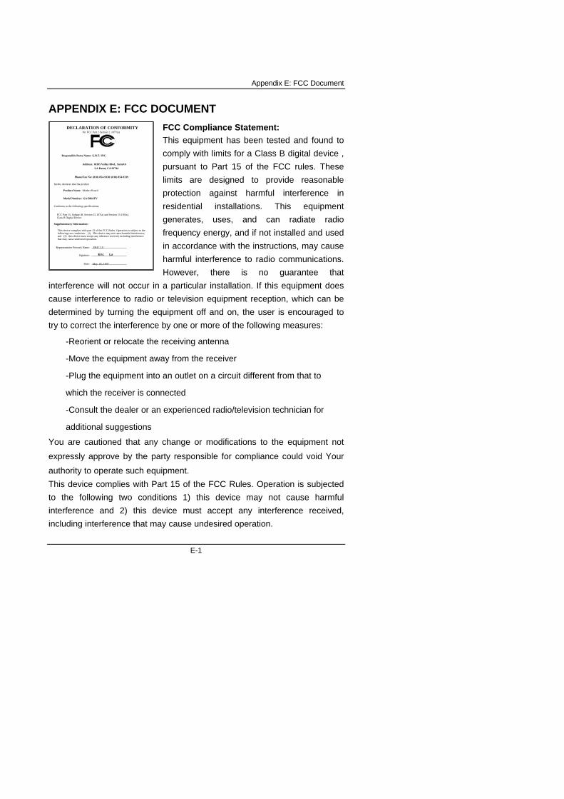
Appendix E: FCC Document
E-1
APPENDIX E: FCC DOCUMENT
FCC Compliance Statement:This equipment has been tested and found to
comply with limits for a Class B digital device ,
pursuant to Part 15 of the FCC rules. These
limits are designed to provide reasonable
protection against harmful interference in
residential installations. This equipment
generates, uses, and can radiate radio
frequency energy, and if not installed and used
in accordance with the instructions, may cause
harmful interference to radio communications.
However, there is no guarantee that
interference will not occur in a particular installation. If this equipment does
cause interference to radio or television equipment reception, which can be
determined by turning the equipment off and on, the user is encouraged to
try to correct the interference by one or more of the following measures:
-Reorient or relocate the receiving antenna
-Move the equipment away from the receiver
-Plug the equipment into an outlet on a circuit different from that to
which the receiver is connected
-Consult the dealer or an experienced radio/television technician for
additional suggestions
You are cautioned that any change or modifications to the equipment not
expressly approve by the party responsible for compliance could void Your
authority to operate such equipment.
This device complies with Part 15 of the FCC Rules. Operation is subjected
to the following two conditions 1) this device may not cause harmful
interference and 2) this device must accept any interference received,
including interference that may cause undesired operation.
DECLARATION OF CONFORMITYPer FCC Part 2 Section 2. 1077(a)
Responsible Party Name: G.B.T. INC.
Address: 18305 Valley Blvd., Suite#A
LA Puent, CA 91744
Phone/Fax No: (818) 854-9338/ (818) 854-9339
hereby declares that the product
Product Name:
Model Number:
Mother Board
GA-586ATV
Conforms to the following specifications:
FCC Part 15, Subpart B, Section 15.107(a) and Section 15.109(a),Class B Digital Device
Supplementary Information:
This device complies with part 15 of the FCC Rules. Operation is subject to thefollowing two conditions: (1) This device may not cause harmful interference,and (2) this device must accept any inference received, including interference that may cause undesired operation.
Representative Person's Name: ERIC LU
Signature:
Date: May. 05, 1997
Eric Lu

GA-586ATV
D-2